Embed Size (px)
Citation preview
Methodology Development of Warpage Analysis of Polymer Based Packaging Substrate
Cheolgyu Kim1, Taeik Lee1, Hyeseon Choi1, Min Sung Kim2, Taek-Soo Kim1
1Department of Mechanical Engineering, KAIST. 373- 291 Daehak-ro (373-1 Guseong-dong), Yuseong-gu, Daejeon 305-
701, Korea. 2Samsung Electro-Mechanics, 25 Samsung-gil,Yeandong-myun,Saejong 339-702,Korea
E-mail: [email protected]
Abstract
Warpage of packaging substrate has been at issue due to
thin and flexible substrate. It is occurred during manufacturing
processes. Although warpage research based on thin metal film
and silicon substrate was actively studied, it has difficulty about
research of polymer based electronic due to its flexibility and
low stiffness compared to metal and silicon substrate. We
suggest a new methodology of warpage analysis to predict the
warpage behavior of polymer composite substrate based
bilayer specimen during temperature rising. The warpage
analysis is performed in the sequence of scanning 3D surface,
calculating curvature and built-in stress of film and verifying
the result using FEM simulation. Two main factors of warpage
behavior are built-in stress in film layer and stress induced by
misfit of coefficient of thermal expansion between film and
substrate. Built-in stress, arisen from built-in strain, is
generated during film lay-up process such as electro-plating of
copper, curing process of polymer. It is computed from the
curvature at room temperature using the strain-curvature
relation. Though this analysis method, the predicted curvature
through temperature cycle showed good agreement with the
experiment.
Introduction
Recently, electronic devices are developed to be multi-
functional, of high performance. Since electronic device trends
to be thinner and smaller than before, Packaging structure in
the various devices could not be avoided to get thinner and
more complex to be asymmetric design. Serious warpage
problem is occurred due to asymmetry design and flexibility of
thin film structure [1, 2]. Thermal processes heat and/or cool
the substrate to be deflected and deformed. Thermal residual
stress is accumulated in the multilayered structure. Packaging
device is disqualified for severe deflection, cannot conduct its
own work. In addition, deformed substrate is frequently stuck
in the manufacturing lines. It cause rate of production to
decrease dramatically. Therefore, it needs to analysis warpage
behavior of packaging substrate.
Displacement between maximum point and minimum
point of specimens, which is called maximum deflection
measurement, were frequently used as warpage standard.
Although, it is easy to measure, it cannot contain any
information about warpage mode and orientation. Therefore,
we adopt curvature, which shows overall shape of specimens,
as warpage standard. Comparison of two methods is shown
Figure 1. Edge of specimen is used for measuring maximum
deflection. It is easily affected by routing condition. Due to this
boundary effect, deflection could not represent accurate
warpage standard. On the contrary, we could gain not only
amount of deflection but also warpage direction and
orientation form the curvature. Coefficient of thermal
expansion (CTE) difference between film and substrate was
previously considered as dominant factor of deformation of
packaging structure [3]. However, deflection caused by room
temperature process was not attributed to CTE misfit.
Film/substrate structure was deformed at room temperature,
although it does not pass through the thermal process.
Therefore, Non-mechanical stress should be studied to
understand the warpage behavior of packaging structure at
room temperature. A number of manufacturing processes
made various intrinsic stresses such as plating stress and curing
stress, thermal stress by CTE. These intrinsic stresses are the
main factors of warpage behavior of room temperature.
To analyze the in-plane stress distribution, proper analytical
solution should consider characteristics of electronic packaging
substrate structure. Stoney’s equation [4] shows basic relation
between curvature and misfit strain with simply equation.
However, commercialized packaging structures have complex
multilayer structure. In the case of PCB, films on the substrate
such as copper circuit, solder resist are not thin compare to the
substrate. Moreover stresses were high enough to make
packaging structure to be severely deformed. Hence, classical
Stoney’s equation [4] is no longer valid to analyze warpage
behavior of packaging substrate.
In this study, we present new analysis method that predicts
curvature of packaging substrate structure by comparing
Figure 1. Warpage calculation methods (a) Maximum
deflection measurement (b) Curvature measurement
978-1-4799-2407-3/14/$31.00 ©2014 IEEE 1004 2014 Electronic Components & Technology Conference
calculated built-in stress on the various films and simulation
result. Built-in stresses were calculated by equation discussed
by Gleskova [5] which is applicable for large deformation case.
Procedure of Warpage Analysis
Figure 2 shows the schematic of procedure of warpage
analysis. To analyze the warpage deformation, curvature
should be calculated in advance. It is necessary to measure the
deformed contour of the warpage. This is a process for
extracting deformation shape of the specimens, the data for
calculating the direction of the warpage (warpage orientation)
and mode of warpage (convex, concave). Contour data is used
for equation fitting. It is possible to calculate the curvatures
through fitted equation. After calculating the curvatures of
specimen, built-in stress is directly calculated by putting the
curvature into analytic model, which is suitable for large
deformation case. Next step is running FEM simulation for
predicting warpage behavior with temperature variation. Built-
in stress and temperature field are applied in simulation model.
Finally, simulation result is verified through the comparing the
actual deformation mode and orientation of experiment result.
Figure 2. Flow diagram of warpage anaylsis
Theoretical Background of Curvature Analysis
Stress measurement in thin film structure based on the
observation of substrate curvature has been developed with
classical Stoney formula and various applications. Stoney’s
theoretical model [4] is well known as most common approach
of getting biaxial stress state from the substrate curvature. The
curvature of Stoney’s equation with thin film in equibiaxial
stress is given as
𝒌𝒔𝒕𝒐𝒏𝒆𝒚 =𝟔𝝈𝒇𝒉𝒇
𝑬′𝒔𝒉𝒔𝟐 (1)
Where 𝜎𝑓 is equibiaxial stress,ℎ𝑓, ℎ𝑠 are thickness film and
substrate and of 𝐸′ is equibiaxial young’s modulus 𝐸/(1 − 𝑣𝑠). However this model is applicable only for limited
case. There are several assumptions to make Stoney’s equation
simple. Substrate has to have uniform thickness and substrate
and films are linear elastic and isotropic. Effects of deposited
film are negligible. The out-of –plane displacement is at least
an order of magnitude less than the substrate thickness.
Therefore, it was impossible to apply Stoney’s equation
directly to our method. If substrate is relatively compliance and
film is highly stressed, film/substrate behaves toward minimize
of the total strain energy. As film intrinsic stress increasing, the
curvature is proportionally increasing with spherical shape of
curvature within linear range. Once film strain becomes large
and overcome the linear range, it is no long maintain its own
shape. It rapidly turns into cylindrical shape with one dominant
curve direction as shown in Figure 3. This phenomenon is
called curvature of bifurcation. The schematic of curvature
bifurcation phenomenon is shown in Figure 4. After curvature
bifurcation, polymer based substrate structure could be
analyzed using analytic model, while the Stoney equation could
not be applicable anymore.
Figure 3. Shapes of specimen with principal curvatures
Figure 4. Curvature bifurcation
Curvature calculation
The equations of the deformed contour from initial state at
the flat surface to the out-of- surface were measured by 3D
scanner. The out-of plane deflections were fitted to an equation
of the 2D polynomial form. Shapes of specimen are categorized
using curvature. Curvature of specimen was calculated by
equation below
𝒌𝜶𝜷 =𝝏𝟐𝒇
𝝏𝒙𝜶𝝏𝒙𝜷·
𝟏
√𝟏+(𝝏𝒇
𝝏𝒙𝜶)𝟐+(
𝝏𝒇
𝝏𝒙𝜷)
𝟐 (2)
For displacement surfaces where the squares of the slopes are
small compared to unity, the curvatures of each axis could be
defined as
𝒌𝒙 =𝝏𝟐𝒇
𝝏𝒙𝟐, 𝒌𝒚 =
𝝏𝟐𝒇
𝝏𝒚𝟐, 𝒌𝒙𝒚 =
𝝏𝟐𝒇
𝝏𝒙𝝏𝒚, 𝒌𝒚𝒙 =
𝝏𝟐𝒇
𝝏𝒚𝝏𝒙 (3)
(𝑥𝛼 = 𝑥, 𝑥𝛽 = 𝑦)
Where z=f(x, y) is specimen contour, the equation of measured
deformed displacement from the flat plane state. 𝑘𝑥 and 𝑘𝑦
are curvatures along two mutually orthogonal x,y directions.
𝑘𝑥𝑦 and 𝑘𝑦𝑥 are defined as twist curvatures which are the rate
1005
of change in slope perpendicular to the direction of travel. Due
to the symmetry of curvature tensor, 𝑘𝑥𝑦 and 𝑘𝑦𝑥 are
theoretically same each other. Principal curvatures could get
using coordinate transformation and removing 𝑘𝑥𝑦 as same
steps to get a maximum and minimum stresses using Mohr
circle.
𝒌𝟏 =𝟏
𝟐[𝒌𝒙 + 𝒌𝒚 + √(𝒌𝒙 − 𝒌𝒚)
𝟐 + 𝟒𝒌𝒙𝒚𝟐 ] (4)
𝒌𝟐 =𝟏
𝟐[𝒌𝒙 + 𝒌𝒚 − √(𝒌𝒙 − 𝒌𝒚)
𝟐 + 𝟒𝒌𝒙𝒚𝟐 ] (5)
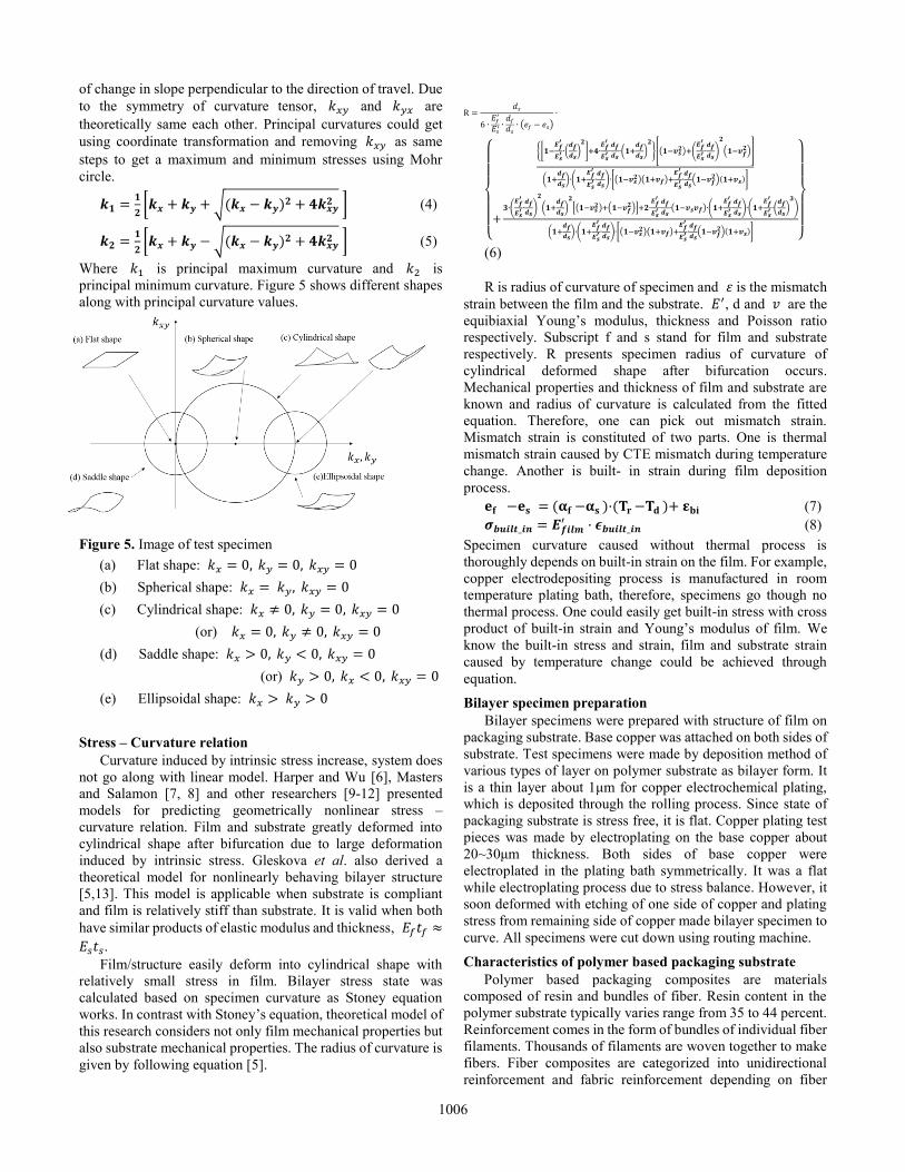
Where 𝑘1 is principal maximum curvature and 𝑘2 is
principal minimum curvature. Figure 5 shows different shapes
along with principal curvature values.
Figure 5. Image of test specimen
(a) Flat shape: 𝑘𝑥 = 0, 𝑘𝑦 = 0, 𝑘𝑥𝑦 = 0
(b) Spherical shape: 𝑘𝑥 = 𝑘𝑦, 𝑘𝑥𝑦 = 0
(c) Cylindrical shape: 𝑘𝑥 ≠ 0, 𝑘𝑦 = 0, 𝑘𝑥𝑦 = 0
(or) 𝑘𝑥 = 0, 𝑘𝑦 ≠ 0, 𝑘𝑥𝑦 = 0
(d) Saddle shape: 𝑘𝑥 > 0, 𝑘𝑦 < 0, 𝑘𝑥𝑦 = 0
(or) 𝑘𝑦 > 0, 𝑘𝑥 < 0, 𝑘𝑥𝑦 = 0
(e) Ellipsoidal shape: 𝑘𝑥 > 𝑘𝑦 > 0
Stress – Curvature relation
Curvature induced by intrinsic stress increase, system does
not go along with linear model. Harper and Wu [6], Masters
and Salamon [7, 8] and other researchers [9-12] presented
models for predicting geometrically nonlinear stress –
curvature relation. Film and substrate greatly deformed into
cylindrical shape after bifurcation due to large deformation
induced by intrinsic stress. Gleskova et al. also derived a
theoretical model for nonlinearly behaving bilayer structure
[5,13]. This model is applicable when substrate is compliant
and film is relatively stiff than substrate. It is valid when both
have similar products of elastic modulus and thickness, 𝐸𝑓𝑡𝑓 ≈
𝐸𝑠𝑡𝑠.
Film/structure easily deform into cylindrical shape with
relatively small stress in film. Bilayer stress state was
calculated based on specimen curvature as Stoney equation
works. In contrast with Stoney’s equation, theoretical model of
this research considers not only film mechanical properties but
also substrate mechanical properties. The radius of curvature is
given by following equation [5].
R =
𝑑𝑠
6 ∙𝐸𝑓′
𝐸𝑠′∙𝑑𝑓𝑑𝑠∙ (𝑒𝑓 − 𝑒𝑠)
∙
{
{[𝟏−
𝑬𝒇′
𝑬𝒔′ ∙(
𝒅𝒇
𝒅𝒔)𝟐
]+𝟒∙𝑬𝒇′
𝑬𝒔′ ∙𝒅𝒇
𝒅𝒔∙(𝟏+
𝒅𝒇
𝒅𝒔)𝟐
}[(𝟏−𝒗𝒔𝟐)+(
𝑬𝒇′
𝑬𝒔′ ∙𝒅𝒇
𝒅𝒔)
𝟐
(𝟏−𝒗𝒇𝟐)]
(𝟏+𝒅𝒇
𝒅𝒔)∙(𝟏+
𝑬𝒇′
𝑬𝒔′ ∙𝒅𝒇
𝒅𝒔)∙[(𝟏−𝒗𝒔
𝟐)(𝟏+𝒗𝒇)+𝑬𝒇′
𝑬𝒔′ ∙𝒅𝒇
𝒅𝒔(𝟏−𝒗𝒇
𝟐)(𝟏+𝒗𝒔)]
+𝟑∙(
𝑬𝒇′
𝑬𝒔′ ∙𝒅𝒇
𝒅𝒔)
𝟐
(𝟏+𝒅𝒇
𝒅𝒔)𝟐
[(𝟏−𝒗𝒔𝟐)+(𝟏−𝒗𝒇
𝟐)]+𝟐∙𝑬𝒇′
𝑬𝒔′ ∙𝒅𝒇
𝒅𝒔∙(𝟏−𝒗𝒔𝒗𝒇)∙(𝟏+
𝑬𝒇′
𝑬𝒔′ ∙𝒅𝒇
𝒅𝒔)∙(𝟏+
𝑬𝒇′
𝑬𝒔′ ∙(
𝒅𝒇
𝒅𝒔)𝟑
)
(𝟏+𝒅𝒇
𝒅𝒔)∙(𝟏+
𝑬𝒇′
𝑬𝒔′ ∙𝒅𝒇
𝒅𝒔)∙[(𝟏−𝒗𝒔
𝟐)(𝟏+𝒗𝒇)+𝑬𝒇′
𝑬𝒔′ ∙𝒅𝒇
𝒅𝒔(𝟏−𝒗𝒇
𝟐)(𝟏+𝒗𝒔)] }
(6)
R is radius of curvature of specimen and 𝜀 is the mismatch
strain between the film and the substrate. 𝐸′, d and 𝑣 are the
equibiaxial Young’s modulus, thickness and Poisson ratio
respectively. Subscript f and s stand for film and substrate
respectively. R presents specimen radius of curvature of
cylindrical deformed shape after bifurcation occurs.
Mechanical properties and thickness of film and substrate are
known and radius of curvature is calculated from the fitted
equation. Therefore, one can pick out mismatch strain.
Mismatch strain is constituted of two parts. One is thermal
mismatch strain caused by CTE mismatch during temperature
change. Another is built- in strain during film deposition
process.
𝐞𝐟 −𝐞𝐬 = (𝛂𝐟 −𝛂𝐬 )·(𝐓𝐫 −𝐓𝐝 )+ 𝛆𝐛𝐢 (7)
𝝈𝒃𝒖𝒊𝒍𝒕_𝒊𝒏 = 𝑬𝒇𝒊𝒍𝒎′ · 𝝐𝒃𝒖𝒊𝒍𝒕_𝒊𝒏 (8)
Specimen curvature caused without thermal process is
thoroughly depends on built-in strain on the film. For example,
copper electrodepositing process is manufactured in room
temperature plating bath, therefore, specimens go though no
thermal process. One could easily get built-in stress with cross
product of built-in strain and Young’s modulus of film. We
know the built-in stress and strain, film and substrate strain
caused by temperature change could be achieved through
equation.
Bilayer specimen preparation
Bilayer specimens were prepared with structure of film on
packaging substrate. Base copper was attached on both sides of
substrate. Test specimens were made by deposition method of
various types of layer on polymer substrate as bilayer form. It
is a thin layer about 1μm for copper electrochemical plating,
which is deposited through the rolling process. Since state of
packaging substrate is stress free, it is flat. Copper plating test
pieces was made by electroplating on the base copper about
20~30μm thickness. Both sides of base copper were
electroplated in the plating bath symmetrically. It was a flat
while electroplating process due to stress balance. However, it
soon deformed with etching of one side of copper and plating
stress from remaining side of copper made bilayer specimen to
curve. All specimens were cut down using routing machine.
Characteristics of polymer based packaging substrate
Polymer based packaging composites are materials
composed of resin and bundles of fiber. Resin content in the
polymer substrate typically varies range from 35 to 44 percent.
Reinforcement comes in the form of bundles of individual fiber
filaments. Thousands of filaments are woven together to make
fibers. Fiber composites are categorized into unidirectional
reinforcement and fabric reinforcement depending on fiber
1006
type. Unidirectional fibers is a bundles of fibers oriented in one
direction. Another is fabric that bundles of fiber are
orthogonally woven. Fabrics make substrate to have
orthotropic property. There are two directions, warp and weft
which are same as the direction of fibers. The warp is the
longitudinal fibers that are under tension of roll, while the weft
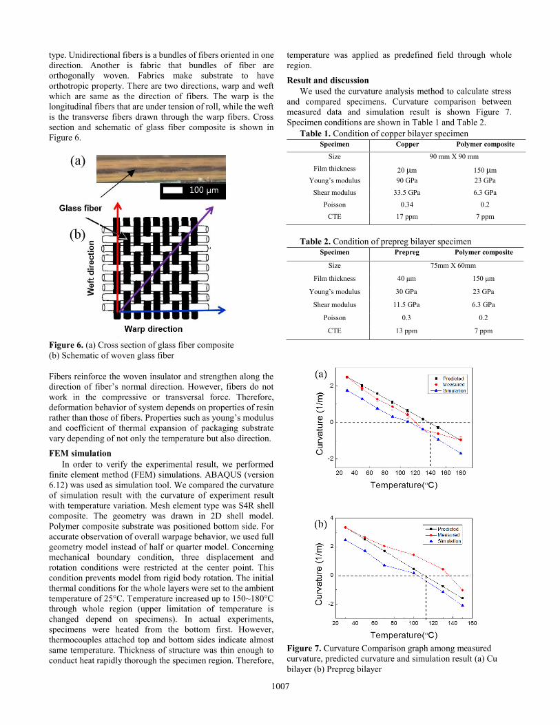
is the transverse fibers drawn through the warp fibers. Cross
section and schematic of glass fiber composite is shown in
Figure 6.
Figure 6. (a) Cross section of glass fiber composite
(b) Schematic of woven glass fiber
Fibers reinforce the woven insulator and strengthen along the
direction of fiber’s normal direction. However, fibers do not
work in the compressive or transversal force. Therefore,
deformation behavior of system depends on properties of resin
rather than those of fibers. Properties such as young’s modulus
and coefficient of thermal expansion of packaging substrate
vary depending of not only the temperature but also direction.
FEM simulation
In order to verify the experimental result, we performed
finite element method (FEM) simulations. ABAQUS (version
6.12) was used as simulation tool. We compared the curvature
of simulation result with the curvature of experiment result
with temperature variation. Mesh element type was S4R shell
composite. The geometry was drawn in 2D shell model.
Polymer composite substrate was positioned bottom side. For
accurate observation of overall warpage behavior, we used full
geometry model instead of half or quarter model. Concerning
mechanical boundary condition, three displacement and
rotation conditions were restricted at the center point. This
condition prevents model from rigid body rotation. The initial
thermal conditions for the whole layers were set to the ambient
temperature of 25°C. Temperature increased up to 150~180°C
through whole region (upper limitation of temperature is
changed depend on specimens). In actual experiments,
specimens were heated from the bottom first. However,
thermocouples attached top and bottom sides indicate almost
same temperature. Thickness of structure was thin enough to
conduct heat rapidly thorough the specimen region. Therefore,
temperature was applied as predefined field through whole
region.
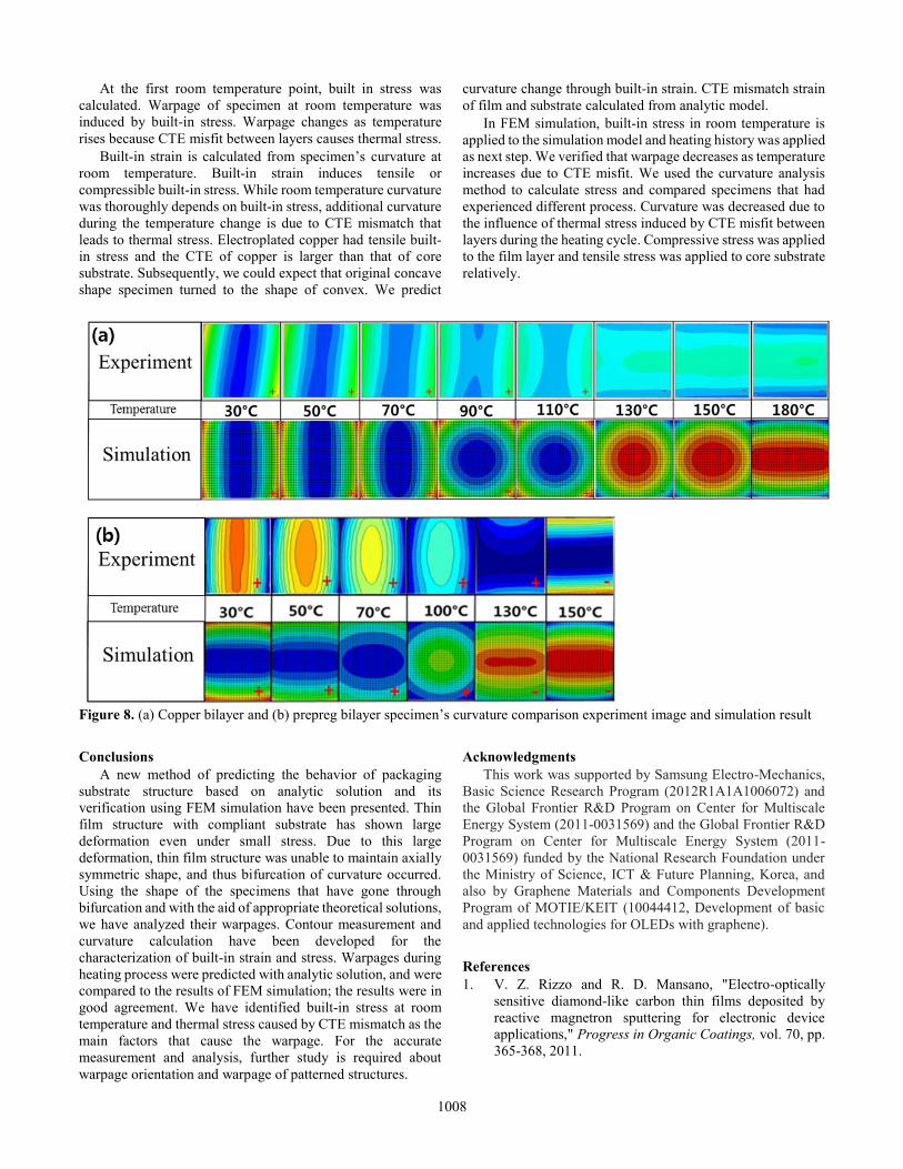
Result and discussion
We used the curvature analysis method to calculate stress
and compared specimens. Curvature comparison between
measured data and simulation result is shown Figure 7.
Specimen conditions are shown in Table 1 and Table 2.
Table 1. Condition of copper bilayer specimen
Specimen Copper Polymer composite
Size 90 mm X 90 mm
Film thickness 20 μm 150 μm
Young’s modulus 90 GPa 23 GPa
Shear modulus 33.5 GPa 6.3 GPa
Poisson 0.34 0.2
CTE 17 ppm 7 ppm
Table 2. Condition of prepreg bilayer specimen
Specimen Prepreg Polymer composite
Size 75mm X 60mm
Film thickness 40 μm 150 μm
Young’s modulus 30 GPa 23 GPa
Shear modulus 11.5 GPa 6.3 GPa
Poisson 0.3 0.2
CTE 13 ppm 7 ppm
Figure 7. Curvature Comparison graph among measured
curvature, predicted curvature and simulation result (a) Cu
bilayer (b) Prepreg bilayer
1007
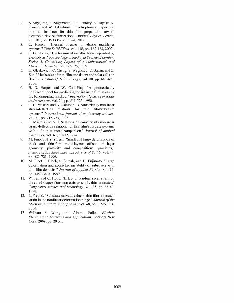
At the first room temperature point, built in stress was
calculated. Warpage of specimen at room temperature was
induced by built-in stress. Warpage changes as temperature
rises because CTE misfit between layers causes thermal stress.
Built-in strain is calculated from specimen’s curvature at
room temperature. Built-in strain induces tensile or
compressible built-in stress. While room temperature curvature
was thoroughly depends on built-in stress, additional curvature
during the temperature change is due to CTE mismatch that
leads to thermal stress. Electroplated copper had tensile built-
in stress and the CTE of copper is larger than that of core
substrate. Subsequently, we could expect that original concave
shape specimen turned to the shape of convex. We predict
curvature change through built-in strain. CTE mismatch strain
of film and substrate calculated from analytic model.
In FEM simulation, built-in stress in room temperature is
applied to the simulation model and heating history was applied
as next step. We verified that warpage decreases as temperature
increases due to CTE misfit. We used the curvature analysis
method to calculate stress and compared specimens that had
experienced different process. Curvature was decreased due to
the influence of thermal stress induced by CTE misfit between
layers during the heating cycle. Compressive stress was applied
to the film layer and tensile stress was applied to core substrate
relatively.
Figure 8. (a) Copper bilayer and (b) prepreg bilayer specimen’s curvature comparison experiment image and simulation result
Conclusions
A new method of predicting the behavior of packaging
substrate structure based on analytic solution and its
verification using FEM simulation have been presented. Thin
film structure with compliant substrate has shown large
deformation even under small stress. Due to this large
deformation, thin film structure was unable to maintain axially
symmetric shape, and thus bifurcation of curvature occurred.
Using the shape of the specimens that have gone through
bifurcation and with the aid of appropriate theoretical solutions,
we have analyzed their warpages. Contour measurement and
curvature calculation have been developed for the
characterization of built-in strain and stress. Warpages during
heating process were predicted with analytic solution, and were
compared to the results of FEM simulation; the results were in
good agreement. We have identified built-in stress at room
temperature and thermal stress caused by CTE mismatch as the
main factors that cause the warpage. For the accurate
measurement and analysis, further study is required about
warpage orientation and warpage of patterned structures.
Acknowledgments
This work was supported by Samsung Electro-Mechanics,
Basic Science Research Program (2012R1A1A1006072) and
the Global Frontier R&D Program on Center for Multiscale
Energy System (2011-0031569) and the Global Frontier R&D
Program on Center for Multiscale Energy System (2011-
0031569) funded by the National Research Foundation under
the Ministry of Science, ICT & Future Planning, Korea, and
also by Graphene Materials and Components Development
Program of MOTIE/KEIT (10044412, Development of basic
and applied technologies for OLEDs with graphene).
References
1. V. Z. Rizzo and R. D. Mansano, "Electro-optically
sensitive diamond-like carbon thin films deposited by
reactive magnetron sputtering for electronic device
applications," Progress in Organic Coatings, vol. 70, pp.
365-368, 2011.
1008
2. S. Miyajima, S. Nagamatsu, S. S. Pandey, S. Hayase, K.
Kaneto, and W. Takashima, "Electrophoretic deposition
onto an insulator for thin film preparation toward
electronic device fabrication," Applied Physics Letters,
vol. 101, pp. 193305-193305-4, 2012.
3. C. Hsueh, "Thermal stresses in elastic multilayer
systems," Thin Solid Films, vol. 418, pp. 182-188, 2002.
4. G. G. Stoney, "The tension of metallic films deposited by
electrolysis," Proceedings of the Royal Society of London.
Series A, Containing Papers of a Mathematical and
Physical Character, pp. 172-175, 1909.
5. H. Gleskova, I. C. Cheng, S. Wagner, J. C. Sturm, and Z.
Suo, "Mechanics of thin-film transistors and solar cells on
flexible substrates," Solar Energy, vol. 80, pp. 687-693,
2006.
6. B. D. Harper and W. Chih-Ping, "A geometrically
nonlinear model for predicting the intrinsic film stress by
the bending-plate method," International journal of solids
and structures, vol. 26, pp. 511-525, 1990.
7. C. B. Masters and N. Salamon, "Geometrically nonlinear
stress-deflection relations for thin film/substrate
systems," International journal of engineering science,
vol. 31, pp. 915-925, 1993.
8. C. Masters and N. J. Salamon, "Geometrically nonlinear
stress-deflection relations for thin film/substrate systems
with a finite element comparison," Journal of applied
mechanics, vol. 61, p. 872, 1994.
9. M. Finot and S. Suresh, "Small and large deformation of
thick and thin-film multi-layers: effects of layer
geometry, plasticity and compositional gradients,"
Journal of the Mechanics and Physics of Solids, vol. 44,
pp. 683-721, 1996.
10. M. Finot, I. Blech, S. Suresh, and H. Fujimoto, "Large
deformation and geometric instability of substrates with
thin-film deposits," Journal of Applied Physics, vol. 81,
pp. 3457-3464, 1997.
11. W. Jun and C. Hong, "Effect of residual shear strain on
the cured shape of unsymmetric cross-ply thin laminates,"
Composites science and technology, vol. 38, pp. 55-67,
1990.
12. L. Freund, "Substrate curvature due to thin film mismatch
strain in the nonlinear deformation range," Journal of the
Mechanics and Physics of Solids, vol. 48, pp. 1159-1174,
2000.
13. William S. Wong and Alberto Salleo, Flexible
Electronics : Materials and Applications, Springer,New
York, 2009, pp. 29-51.
1009


![Warpage Mechanism of Thin Embedded LSI Packages · 2013. 7. 3. · 47 [Technical Paper] Warpage Mechanism of Thin Embedded LSI Packages Yoshiki Nakashima*, Katsumi Kikuchi*, Kentaro](https://img.pdfslide.net/doc/110x75/60eee77b52764269737825c9/warpage-mechanism-of-thin-embedded-lsi-2013-7-3-47-technical-paper-warpage.jpg)