Embed Size (px)
Citation preview

8/7/2019 Metodos_PCB
http://slidepdf.com/reader/full/metodospcb 1/54
EMC-TI101-R
16215 Alton Parkway P.O. Box 57013 • Irvine, CA 92619-7013 • Phone: 949-450-8700 • Fax: 949-450-8710 10/07/04
Technical Information
Selected Methods for Low-Noise Printed CircuitBoard Design
Neven Pischl

8/7/2019 Metodos_PCB
http://slidepdf.com/reader/full/metodospcb 2/54
Broadcom® and the pulse logo are trademarks of Broadcom Corporation and/or its subsidiaries in the United States and
certain other countries. All other trademarks mentioned are the property of their respective owners.
Broadcom CorporationP.O. Box 57013
16215 Alton Parkway
Irvine, CA 92619-7013
© 2004 by Broadcom CorporationAll rights reserved
Printed in the U.S.A.
REVISION HISTORY
Revision Date Change Description
EMC-TI101-R 10/07/04 Update to revision 1
EMC-TI100-R 06/05/03 Initial release.

8/7/2019 Metodos_PCB
http://slidepdf.com/reader/full/metodospcb 3/54
Technical Information10/07/04
Broadcom Corporation
Document EMC-TI101-R Page iii
TABLE OF CONTENTS
Introduction .................................................................................................................................................. 2
Currents, Voltages, EM Field, and Frequency Spectra ............................................................................. 3
Currents and EM Fields .......................................................................................................................... 3Voltages and Currents in Time and Frequency Domains ....................................................................... 5
Effect of Duty-Cycle ......................................................................................................................... 6
Effect of Rise and Fall Time............................................................................................................. 7
Current vs. Voltage Spectrum.......................................................................................................... 8
Intentional Signals ..................................................................................................................................... 11
Single-Ended and True-Differential Signals.......................................................................................... 11
Microstrip Transmission Line and Current Distribution ......................................................................... 12
Differential Mode Radiation and Susceptibility...................................................................................... 15
Discontinuity in the Current Path .......................................................................................................... 16
Routing Across a Slot in the Plane ................................................................................................ 16
Changing PCB Layers ................................................................................................................... 19
Connecting Two or More PCBs ..................................................................................................... 20
Edges of the Planes.............................................................................................................................. 21
Traces Close to the Edges of the Planes ...................................................................................... 21
EM Field Propagation at the Edges of the Planes ......................................................................... 23
Unintentional Currents and Voltages ....................................................................................................... 25
Common Mode Voltage and Current .................................................................................................... 25Sources.......................................................................................................................................... 25
Radiation from CM Currents .......................................................................................................... 28
Reducing Emission from CM Currents........................................................................................... 29
Crosstalk ............................................................................................................................................... 29
Switching Noise Between Vcc and L0 Planes ...................................................................................... 30
Decoupling and Bypassing ....................................................................................................................... 33
Ideal and Real Capacitors..................................................................................................................... 34
Inductance ............................................................................................................................................ 35
Parallel Capacitors................................................................................................................................ 37
Board Stackup ............................................................................................................................................ 39
12-Layer Example................................................................................................................................. 39
Discussion of the 12-Layer Example Stackup Features................................................................ 40
Return Paths .......................................................................................................................... 40

8/7/2019 Metodos_PCB
http://slidepdf.com/reader/full/metodospcb 4/54
Technical Information10/07/04
Broadcom Corporation
Page iv Document EMC-TI101-R
Characteristic Impedances .....................................................................................................40
Crosstalk ................................................................................................................................40
Coupling Between Vcc and L0 Planes ...................................................................................41
Coupling Between Signal Currents and Power Supply Currents (Crosstalk Between Signals
and Power) .............................................................................................................................41Split Vcc Planes .....................................................................................................................42
Reducing the Number of PCB Layer Trade-Offs...................................................................................42
Return Paths ..........................................................................................................................43
Crosstalk ................................................................................................................................43
Coupling Between Vcc and L0 Planes ...................................................................................43
Coupling Between Signal and Power Supply Currents ..........................................................44
References and Literature .........................................................................................................................48
References ............................................................................................................................................48
Literature ...............................................................................................................................................48

8/7/2019 Metodos_PCB
http://slidepdf.com/reader/full/metodospcb 5/54
Technical Information10/07/04
Broadcom Corporation
Document EMC-TI101-R Page v
LIST OF FIGURES
Figure 1: Hertzian Dipole.................................................................................................................................... 3
Figure 2: Trapezoidal Pulse Train in Time Domain ............................................................................................ 5
Figure 3: Slight Deviation from 50% Duty-Cycle Cause Significant Increase of Odd Harmonics....................... 6Figure 4: Relative Amplitude of Trapezoidal Pulse Train Harmonics with Different Rise Times ........................ 7
Figure 5: Series (Source) and Parallel (Load) Termination of Digital Transmission Lines ................................. 8
Figure 6: Source Voltage (VS) and Load Voltages (VLS and VLP) with Series and Parallel Termination ......... 9
Figure 7: Current with Series and Parallel Termination (IS and IP).................................................................... 9
Figure 8: Frequency Spectra of IS and IP ........................................................................................................ 10
Figure 9: Examples of Intentional Signals Often Referred to as Differential in EMI Context ............................ 11
Figure 10: Current Density Distribution in an Infinite Plane Under a Microstrip Trace and Magnetic Field
Lines ................................................................................................................................................................. 12
Figure 11: Simplified Model of a Two-Conductor Uniform Transmission Line.................................................. 13
Figure 12: Transmission Line with Elements Assigned to Return Path ............................................................ 14
Figure 13: Far-Field Electric Field from a Loop High Above Conductive Plane ............................................... 15
Figure 14: Continuous and Broken Current Paths for a Trace Above a Plane and Approximate Current Density
Distribution in the Plane, Across the Slot and Perpendicular to the Trace ....................................................... 16
Figure 15: Model of a Transmission Line Running Across a Slot in Plane....................................................... 17
Figure 16: Routing Traces Across a Slot Significantly Increases Crosstalk Between Them............................ 18
Figure 17: Cross-Section of a PCB Shows Discontinuous Current Path Due to Change of Layers................. 19
Figure 18: Example of Routing High-Speed or Susceptible Traces ................................................................. 20

8/7/2019 Metodos_PCB
http://slidepdf.com/reader/full/metodospcb 6/54
Technical Information10/07/04
Broadcom Corporation
Page vi Document EMC-TI101-R
Figure 19: Current Density Distribution in a Finite Plane Under Microstrip when the Trace is Close to the
Edge..................................................................................................................................................................21
Figure 20: Dipole Model of Radiation Due to CM Impedance of a Plane..........................................................22
Figure 21: Pulling the Vcc Planes and Stitching the L0 Planes with Vias at the Edges ....................................24
Figure 22: CM Current Due to Impedance of Ground Return ...........................................................................25Figure 23: CM Due to Impedance of L0 Lead—Ground Bounce ......................................................................26
Figure 24: CM Due to Load Imbalance in True Differential Circuits..................................................................27
Figure 25: CM Currents on Cables Radiate Efficiently......................................................................................28
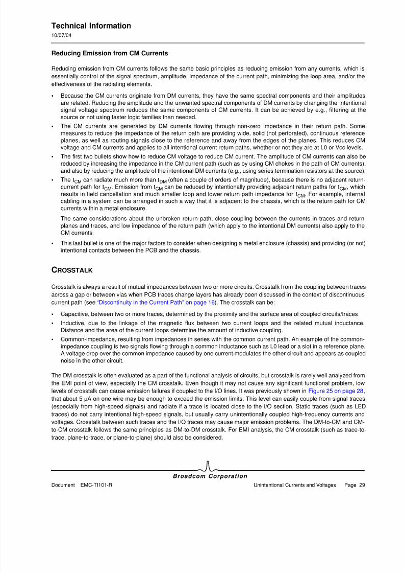
Figure 26: Signal Current and Cross-Conduction Current Surges Example.....................................................31
Figure 27: Ferrite Beads in Power Supply of Noisy Components Attenuate Noise Propagation on PCB.........32
Figure 28: Series and Parallel RLC Circuits .....................................................................................................34
Figure 29: Relative Impedance of C, L, Series, and Parallel RLC Circuits Versus Frequency .........................34
Figure 30: Minimizing Inductance by Arranging Vias for Minimum Loop Area (Shaded) ..................................35
Figure 31: Inductance of a Rectangular Loop, Dimensions in Inches...............................................................35
Figure 32: Measured Impedance of a 0.1 µF Ceramic (X7R) Capacitor with Different PCB-LayoutInductances.......................................................................................................................................................36
Figure 33: Impedance of Two Parallel Capacitors and Each Individual Capacitor ...........................................37
Figure 34: 12-Layer PCB Stackup Example .....................................................................................................39
Figure 35: High-Frequency Current in Power Distribution and Signal Current Do Not Flow Through Common
Impedance in this Arrangement of PCB Layers Due to Skin Effect ..................................................................41
Figure 36: 10-Layer Stackup Example for Discussion ......................................................................................43
Figure 37: Mechanism of High-Frequency Noise Coupling Between Power Distribution System and Routing
Layers when Routing is Between Vcc and L0 Planes .......................................................................................44Figure 38: Improving Performance by Adding L0 Fills ......................................................................................45
Figure 39: Six-Layer Stackup with Two Internal Routing Layers ......................................................................46
Figure 40: Six-Layer Stackup with Improved Performance...............................................................................47

8/7/2019 Metodos_PCB
http://slidepdf.com/reader/full/metodospcb 7/54
Technical Information10/07/04
Broadcom Corporation
Document EMC-TI101-R Page 1
“Due to the brilliance of the flash one tends to believe that all current just disappears in the soil. Based on this Franklin developed the lightning protection, a grounded iron rod.
Thus an incorrect conception of grounding was firmly rooted; it lived for more than 200 years and generates even nowadays a major problem in EMC.”
Grounding Philosophy, P.C.T. Van der Laan, M.A. Van Houten and A.P.J. Van Deursen
Seventh International Zurich Symposium on EMC, March 1987
8/7/2019 Metodos_PCB
http://slidepdf.com/reader/full/metodospcb 8/54
Technical Information10/07/04
Broadcom Corporation
Page 2 Introduction Document EMC-TI101-R
INTRODUCTION
This document was originally created as a description of some of the basic concepts in design for electromagnetic
compatibility (EMC). The described techniques apply not only to the EMC-design. They are generally good practices for
noise suppression by careful printed circuit board (PCB) design. In that sense, the term Electromagnetic Interference (EMI)is more appropriate, describing various noise phenomena, including emission, susceptibility, crosstalk, and noise on the
power distribution. The intention of this document is to:
Show how the selected design techniques relate to fundamental concepts (e.g., current cancellation and inductance)
• Help readers acquire an intuitive understanding of the principles that define noise and EMI performance of a product
• Provide a concise reference for the electronic products designers interested in noise suppression at the PCB level
The applicable theory needed for understanding the principles behind the described material is highlighted. A deep and
comprehensive theoretical analysis of all related design aspects is beyond the scope of this document. Several references
used in preparing this text are given.
The emphasis within this document is given to the PCB-level design methods, because the PCB is often the critical design
segment that affects noise, e.g. power supply noise, crosstalk, and EMI. All considerations revolve around a few concepts,such as current flow and its path, Electromagnetic (EM) field cancellation, CM and differential-mode (DM) currents, and low-
impedance current return paths. The same concepts that govern the design at the PCB level are also fundamental to
designing at the system level.
There are many different sources and mechanisms of noise and EMI coupling that are often poorly characterized in a typical
electronic system, which makes the analysis or simulation difficult. In most cases, each contributor to the overall
performance is easy to understand. What gives it a complexity is the total number of mutually interacting factors that
determine the noise-related performance, many of them being parasitics. From the functional design point of view, the
combination and interaction of these factors is unintentional. Because of this, they are often not well-understood and not the
subject of study.
Understanding noise and EMI is a multi-disciplinary field, involving high-frequency design, analog, digital, power supply,
mechanical design, and associated technologies. A combination of the theoretical knowledge, experience, analysis of theknown and unspecified design parameters, and application of the fundamental design principles are necessary for
successful noise control by design.
Ultimately, successful performance of a product is derived by detailed integration of all of the required parameters. While
this document cannot assure that the required performance will result, it is offered to provide instructions of some of methods
of reducing noise, crosstalk, and EMI in circuit board design.
8/7/2019 Metodos_PCB
http://slidepdf.com/reader/full/metodospcb 9/54
Technical Information10/07/04
Broadcom Corporation
Document EMC-TI101-R Currents, Voltages, EM Field, and Frequency Spectra Page 3
CURRENTS, VOLTAGES, EM FIELD, AND FREQUENCY SPECTRA
CURRENTS AND EM FIELDS
Intentional signals are usually well understood and taken care of during design. Unfortunately, the intentional currents
generate unintentional results due to non-ideal properties of the real components (some of them called parasitics), PCB, and
used materials. Noise suppression mostly deals with unintentional currents, voltages, and impedances, whether or not they
are generated by:
• Intentional signals, causing emissions and interferences
• Some external source that causes EMI and susceptibility of electronic equipment, such as electrostatic discharges
(ESD) or nearby radio frequency (RF) fields
The most important design consideration is to realize that almost all noise and EMI phenomena and design methods are
directly related to the magnitude, frequency spectrum, and path (size and shape of the loops) of the current. The magnitude
of the currents and the paths in which they flow must be properly designed for both intentional and unintentional currents.
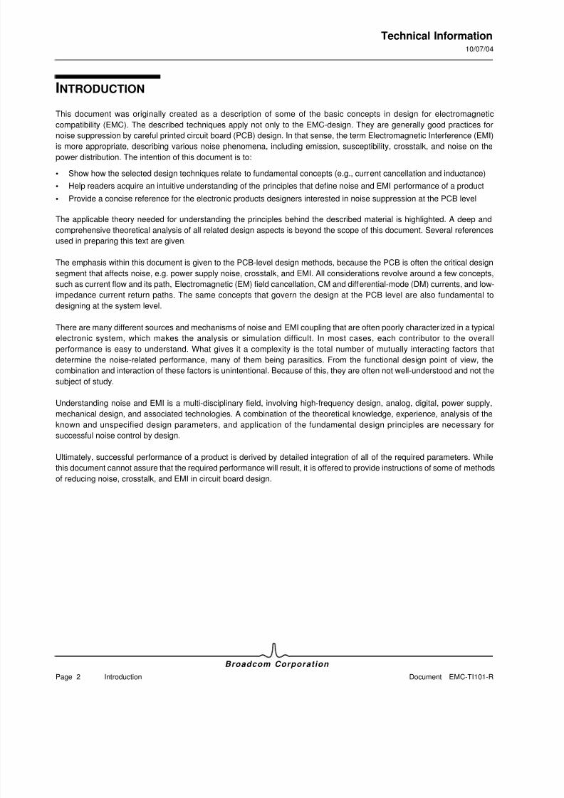
The Hertzian dipole is useful to describe the fundamental relations between the current and the EM field. It is an infinitesimal
current element carrying time-varying current i(t). Because the element is short, it can be assumed that the current
distribution is constant along its length of dl. It can be shown that such a short element of current generates a radial EM
wave with the maximum in direction perpendicular to its axis. Figure 1 describes the far-field EM components EMAX and
HMAX in the direction of maximum radiation, at the distance r from the Hertzian dipole.
Figure 1: Hertzian Dipole
I Current in the Hertzian dipole
η0 Intrinsic impedance of the propagation medium (η0 = 120π Ω in vacuum)
β0 = 2π/ λ Phase constant
λ Wavelength
r Distance from the Hertzian dipole
dl
I
r
EMAX = η0β0 Idl / (4 πr)
HMAX = EMAX / η0

8/7/2019 Metodos_PCB
http://slidepdf.com/reader/full/metodospcb 10/54
Technical Information10/07/04
Broadcom Corporation
Page 4 Currents, Voltages, EM Field, and Frequency Spectra Document EMC-TI101-R
The time-varying current generates both EM field components. The voltage is not explicit in the relations that describe the
EM field. The field strength increases with the current and length of the current element, and decreases inversely
proportional to the distance. After some distance from the source, the E and H components of the EM field are orthogonal
to each other and to the direction of the EM-wave propagation. The E and H fields are related to each other by the intrinsic
impedance η0 of the medium, H=E/ η0.
From the aforementioned, in real electrical circuits, for every current flowing in one direction there must be current flowing
in the opposite direction to close the loop. The current loop defines the impedance of the current path. Except for the DC
and low frequencies in the audio range, the impedance is dominated by the inductance of the current path.
A current loop can be modeled as a number of Hertzian dipoles that make the entire loop. The resulting EM field in the
surrounding space is a superposition of contributions from each of the Hertzian dipoles. If two elements of the loop are
parallel to each other and carry currents of the same amplitude in opposite directions, they tend to cancel each other’s EM
field. At the limit case, if both current elements occupy exactly the same space, the resulting total current is zero and does
not produce any EM field. This leads to another key principle:
Antenna theory shows that all passive antennas are reciprocal. Poor transmitting antennas are also poor receiving antennas.
Reducing emission by building inefficient radiating structures tends to reduce reception of external interferences as well. This
explains the next principle for design to minimize EMI:
Nearly all noise, crosstalk, and EMI generation and coupling mechanisms, and design principles for low noise have
something to do with the fact that (again) all currents flow in loops. Designing electronic systems for low EMI and low-noise
requires recognizing where currents flow and which loops (paths) they take, and managing the amplitudes, paths, and
impedances associated with them. As it is shown throughout this document, this management of current flow is the most
effective way of designing for low-noise and EMI. This can be applied to transmission lines, decoupling, grounding, selection
of a PCB stackup, or some of many other topics and methods of design. The design engineer should always remember the
principles about currents flowing in the loops, and the EM field cancellation that reduces noise generation, coupling, emission
and susceptibility to EMI. It is also important to remember that the same principles apply to the intentional as well as the
unintentional currents. While crosstalk and noise on the power distribution system are analyzed more often, the EMI
problems often arise because the unintentional currents and these principles are ignored.
EM radiation is proportional to the current and length of the current element.The Hertzian dipole is useful to describe relations between the current elements and EM fields, but such an isolated
current-carrying element does not exist. Currents exist as a consequence of a voltage across some impedance (load),
and all currents must flow in closed loops between the source and the load. The size and shape of the loops can vary,
which does not change the principle that all currents flow in closed loops. Current sinks do not exist .
Two adjacent currents of equal magnitude flowing in opposite directions minimize the total generated EM field.
Measures taken to minimize emission usually also minimize susceptibility to external EMI.
8/7/2019 Metodos_PCB
http://slidepdf.com/reader/full/metodospcb 11/54
Technical Information10/07/04
Broadcom Corporation
Document EMC-TI101-R Currents, Voltages, EM Field, and Frequency Spectra Page 5
VOLTAGES AND CURRENTS IN TIME AND FREQUENCY DOMAINS
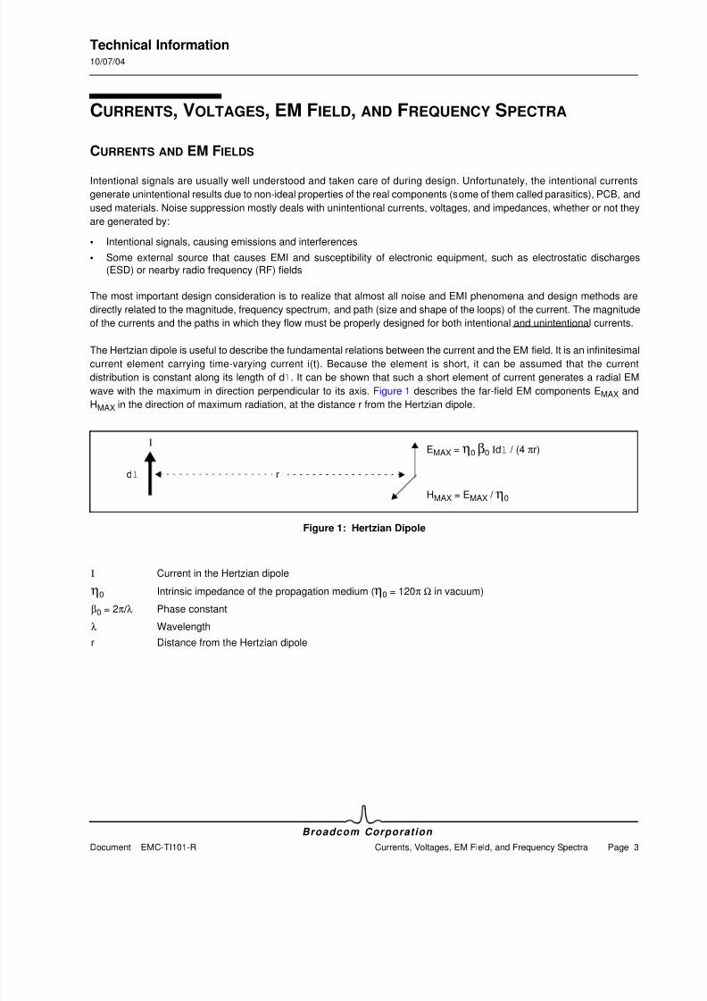
Digital signals are voltage pulses with exponential rise and fall edges, which can be approximated by trapezoidal voltage
pulses. They are defined in the time domain by their amplitude, rise time, fall time, duration, and period or frequency as
depicted in Figure 2. It can be shown that such repetitive signals can also be represented in the frequency domain, with their
frequency components (harmonics) each having its frequency, amplitude, and phase. A constant value (DC component) is
superimposed to the harmonics.
Figure 2: Trapezoidal Pulse Train in Time Domain
A pulse train with the period T, pulse duration τ, amplitude A, and rise time equal to the fall time tR = tF can be described as:
∞X(t) = c0 + Σ | cn | cos (ωnt + Φn)
n = 1
cn = Amplitude of the n-th harmonic.
fn = n/T = Frequency of the n-th harmonic.
Φn= Phase of the n-th harmonic.
ωn = 2πfn
c0 = A τ/T = DC component of the pulse train.
T
tR
tF
τ
A
t
8/7/2019 Metodos_PCB
http://slidepdf.com/reader/full/metodospcb 12/54
Technical Information10/07/04
Broadcom Corporation
Page 6 Currents, Voltages, EM Field, and Frequency Spectra Document EMC-TI101-R
Effect of Duty-Cycle
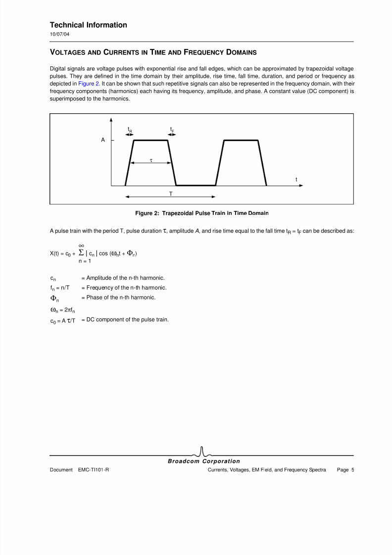
The harmonics are cosine functions with the amplitude cn and the period ωn = 2πfn. The fn are multiples of the pulse
repetition frequency f = 1/T. The pulse train is represented in the frequency domain with a DC-component (c0) and harmonics
at every multiple of the pulse fundamental frequency f = 1/T. If T/ τ = 0.5 (50% duty cycle), then the even multiples of the
fundamental frequency disappear. If not, the even harmonics are present and can be strong for even a small deviation from
50% duty cycle as shown in the following figure. An example of the spectra with T/ τ = 0.5 and T/ τ = 0.49 is shown in Figure 3,for tR=tF =0.01T.
Figure 3: Slight Deviation from 50% Duty-Cycle Cause Significant Increase of Odd Harmonics
Relative
Amplitude, 20 dB/div
Harmonic number(~ frequency)
Harmonic number(~ frequency)
T/ τ = 0.49T/ τ = 0.5
1 2 3 4 5 6 10 20 301 2 3 4 5 6 10 20 30
8/7/2019 Metodos_PCB
http://slidepdf.com/reader/full/metodospcb 13/54
Technical Information10/07/04
Broadcom Corporation
Document EMC-TI101-R Currents, Voltages, EM Field, and Frequency Spectra Page 7
Effect of Rise and Fall Time
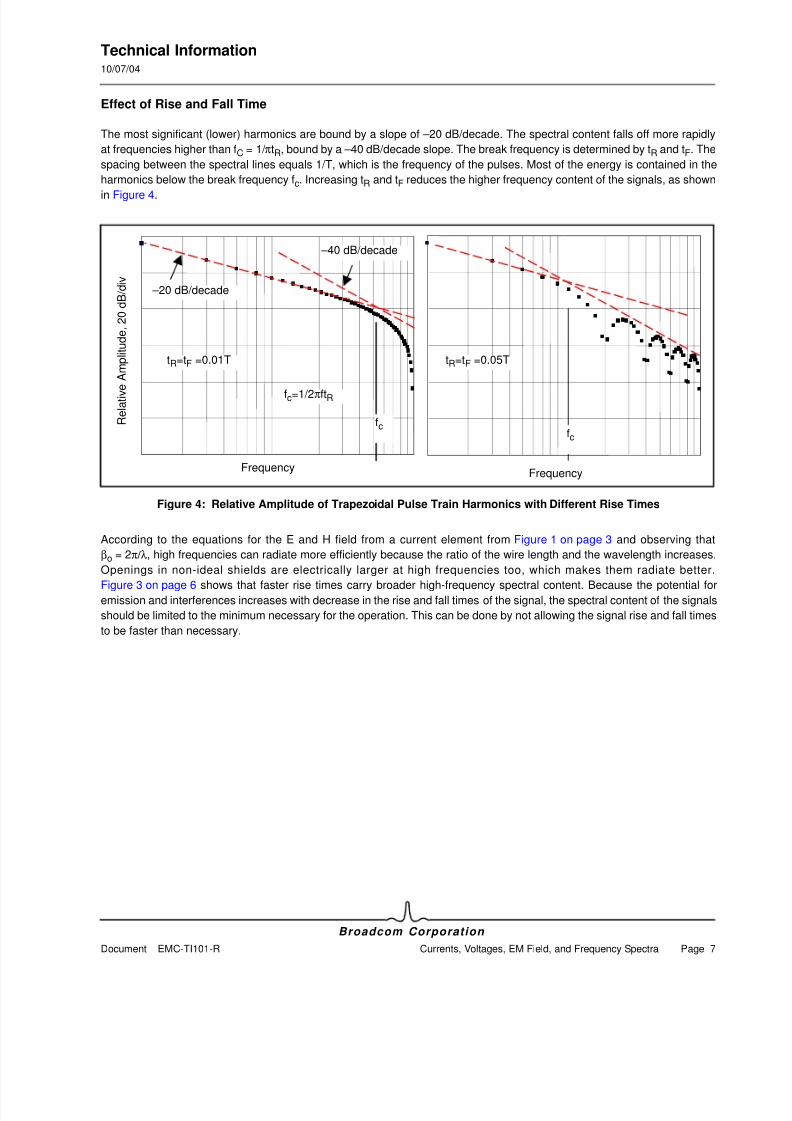
The most significant (lower) harmonics are bound by a slope of –20 dB/decade. The spectral content falls off more rapidly
at frequencies higher than fC = 1/ πtR, bound by a –40 dB/decade slope. The break frequency is determined by tR and tF. The
spacing between the spectral lines equals 1/T, which is the frequency of the pulses. Most of the energy is contained in the
harmonics below the break frequency fc. Increasing tR and tF reduces the higher frequency content of the signals, as shown
in Figure 4.
Figure 4: Relative Amplitude of Trapezoidal Pulse Train Harmonics with Different Rise Times
According to the equations for the E and H field from a current element from Figure 1 on page 3 and observing that
βo = 2π/ λ, high frequencies can radiate more efficiently because the ratio of the wire length and the wavelength increases.
Openings in non-ideal shields are electrically larger at high frequencies too, which makes them radiate better.
Figure 3 on page 6 shows that faster rise times carry broader high-frequency spectral content. Because the potential for
emission and interferences increases with decrease in the rise and fall times of the signal, the spectral content of the signals
should be limited to the minimum necessary for the operation. This can be done by not allowing the signal rise and fall times
to be faster than necessary.
Relative
Amplitude, 20 dB/div
FrequencyFrequency
–20 dB/decade
–40 dB/decade
tR=tF =0.01T
fc=1/2πftR
fcfc
tR=tF =0.05T
8/7/2019 Metodos_PCB
http://slidepdf.com/reader/full/metodospcb 14/54
Technical Information10/07/04
Broadcom Corporation
Page 8 Currents, Voltages, EM Field, and Frequency Spectra Document EMC-TI101-R
Current vs. Voltage Spectrum
As it follows from the relation between the current and the EM field in Figure 1 on page 3, the magnitude of the current and
its spectral content are critical to noise coupling, but it is the voltage waveform that is normally of a concern for the system
designers. The voltage waveform often does not disclose much of the current waveform, magnitude, and spectral content.
However, the current is the determining factor for the noise and EMI performance in most PCBs and devices.
Used to reduce reflections, transmission line termination also significantly influences the spectral amplitudes of the current
in the traces, which influences emission from the traces and crosstalk. The two most frequently used line termination
schemes are series (or source) and parallel (or load) termination. Even though both schemes can result in acceptable
voltage waveform at the load (which is the objective of the functional design), the current waveform and frequency content
can be significantly different for these two termination schemes. All clocks and high-speed signals are usually terminated
with either series or parallel terminating resistors. In principle, the series termination is more appropriate for single-load clock
distribution, while parallel termination is better suited to multiple loads distributed evenly along the line.
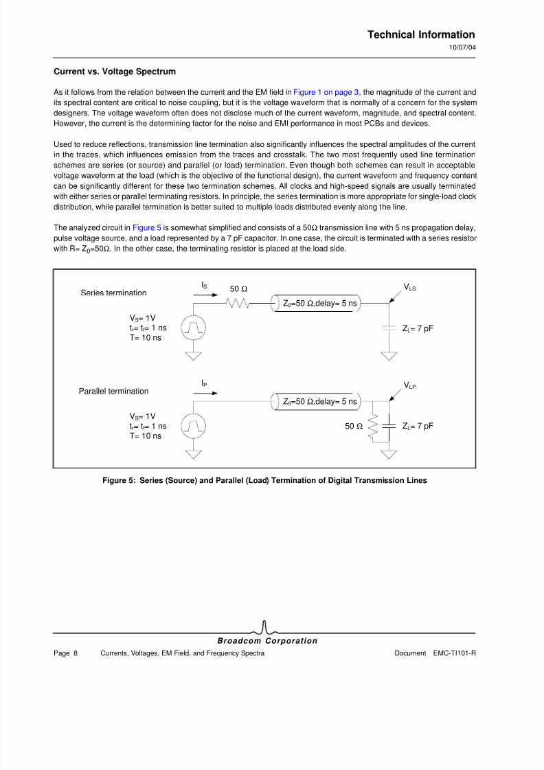
The analyzed circuit in Figure 5 is somewhat simplified and consists of a 50Ω transmission line with 5 ns propagation delay,
pulse voltage source, and a load represented by a 7 pF capacitor. In one case, the circuit is terminated with a series resistor
with R= Z0=50Ω. In the other case, the terminating resistor is placed at the load side.
Figure 5: Series (Source) and Parallel (Load) Termination of Digital Transmission Lines
50 Ω
Z0=50 Ω,delay= 5 ns
IS
VS= 1Vtr= tf= 1 ns
T= 10 nsZL= 7 pF
VLSSeries termination
50 Ω
Z0=50 Ω,delay= 5 ns
IP
VS= 1Vtr= tf= 1 nsT= 10 ns
ZL= 7 pF
VLPParallel termination
8/7/2019 Metodos_PCB
http://slidepdf.com/reader/full/metodospcb 15/54
Technical Information10/07/04
Broadcom Corporation
Document EMC-TI101-R Currents, Voltages, EM Field, and Frequency Spectra Page 9
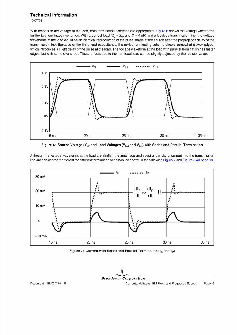
With respect to the voltage at the load, both termination schemes are appropriate. Figure 6 shows the voltage waveforms
for the two termination schemes. With a perfect load (ZL = Z0, and C = 0 pF) and a lossless transmission line, the voltage
waveforms at the load would be an identical reproduction of the pulse shape at the source after the propagation delay of the
transmission line. Because of the finite load capacitance, the series-terminating scheme shows somewhat slower edges,
which introduces a slight delay of the pulse at the load. The voltage waveform at the load with parallel termination has faster
edges, but with some overshoot. These effects due to the non-ideal load can be slightly adjusted by the resistor value.
Figure 6: Source Voltage (VS) and Load Voltages (VLS and VLP) with Series and Parallel Termination
Although the voltage waveforms at the load are similar, the amplitude and spectral density of current into the transmission
line are considerably different for different termination schemes, as shown in the following Figure 7 and Figure 8 on page 10.
Figure 7: Current with Series and Parallel Termination (IS and IP)
1.2V
–0.4V
0V
0.8V
15 ns 20 ns 25 ns 30 ns 35 ns
VS VLS VLP
0.4V
IS IP
0
20 mA
15 ns 20 ns 25 ns 30 ns 35 ns
10 mA
30 mA
–10 mA
>>dI
P
dt
dIS
dt !!
8/7/2019 Metodos_PCB
http://slidepdf.com/reader/full/metodospcb 16/54
Technical Information10/07/04
Broadcom Corporation
Page 10 Currents, Voltages, EM Field, and Frequency Spectra Document EMC-TI101-R
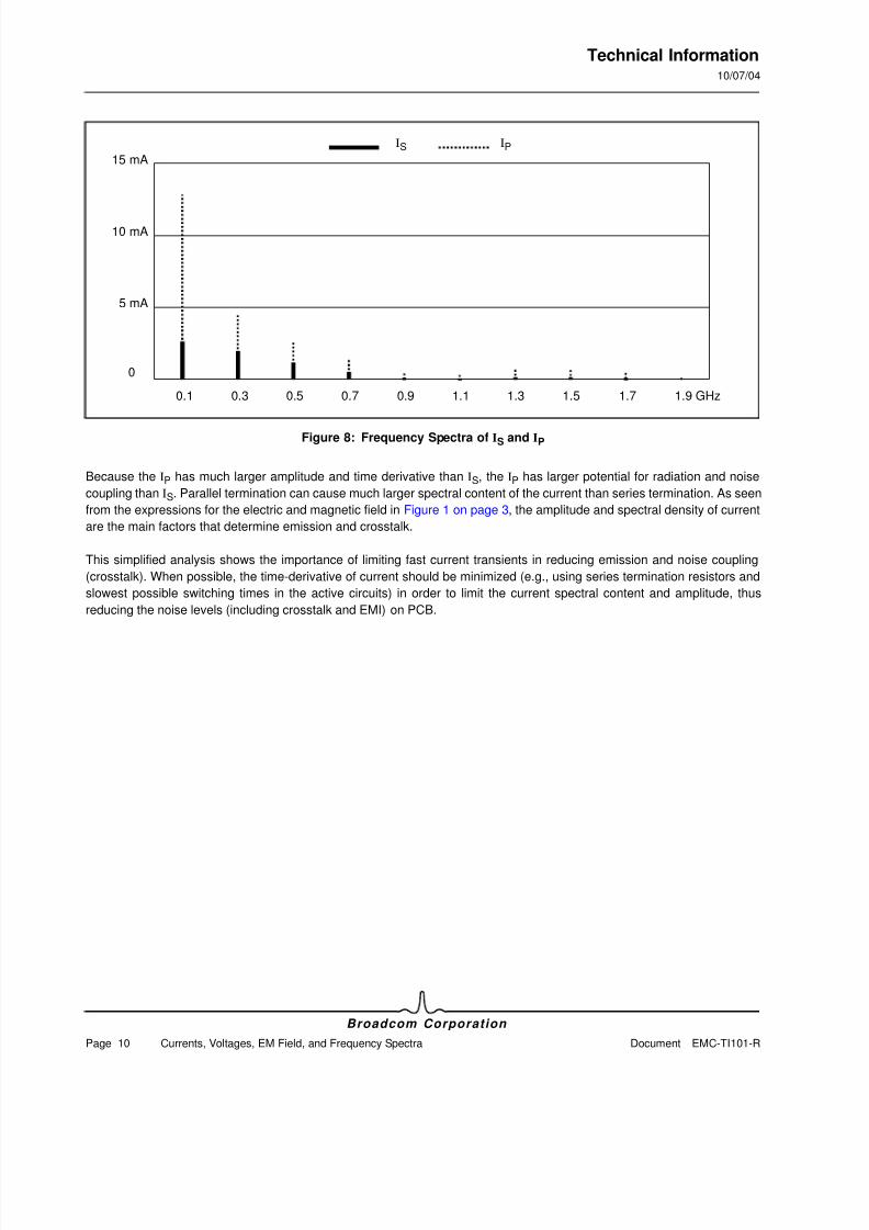
Figure 8: Frequency Spectra of IS and IP
Because the IP has much larger amplitude and time derivative than IS, the IP has larger potential for radiation and noise
coupling than IS. Parallel termination can cause much larger spectral content of the current than series termination. As seen
from the expressions for the electric and magnetic field in Figure 1 on page 3, the amplitude and spectral density of current
are the main factors that determine emission and crosstalk.
This simplified analysis shows the importance of limiting fast current transients in reducing emission and noise coupling
(crosstalk). When possible, the time-derivative of current should be minimized (e.g., using series termination resistors and
slowest possible switching times in the active circuits) in order to limit the current spectral content and amplitude, thus
reducing the noise levels (including crosstalk and EMI) on PCB.
IS IP
0
10 mA
0.1 0.3 0.5 0.7 1.9 GHz
5 mA
15 mA
0.9 1.1 1.3 1.5 1.7
8/7/2019 Metodos_PCB
http://slidepdf.com/reader/full/metodospcb 17/54
Technical Information10/07/04
Broadcom Corporation
Document EMC-TI101-R Intentional Signals Page 11
INTENTIONAL SIGNALS
SINGLE-ENDED AND TRUE-DIFFERENTIAL SIGNALS
When discussing different signal types, it is worth noticing that in EMI jargon, the term “differential signal” does not always
mean true-differential signal. In EMI context, differential signals can be intentional signals of two kinds:
• Single-ended or “imbalanced” signals, between a signal node and a reference potential (“ground”, logic 0, or reference)
• True-differential or “balanced” signals, where two conductors carry a signal with no reference to “ground” or logic 0
Thus, whether single-ended or true-differential, in EMI context all intentional signals are often called differential, and the
mode of intentional-signal propagation is called differential mode (DM) in either case.
The term ground is commonly and inappropriately used to describe the conductor with 0V or reference (logic zero) voltage
level. Ground is one of the paths where the intentional current (as well as the unintentional current) completes its loop. The
term return path is also often used for the same purpose to describe the segment of the current loop other than the signal
trace. Instead of the term ground , the term L0 (logic zero) is more appropriate for the intentional 0V reference on the PCB.
Similarly, the power supply planes and traces that are at a DC voltage level relative to L0 will be described as Vcc instead
of the commonly used term power planes and traces.
The current flows in loops formed by conductors. In single-ended systems, one conductor is typically a signal trace or wire.
The other is another trace or a plane, ideally at the reference voltage (often at 0V). The intended return path in the single-
ended systems is through the signal traces and reference planes or traces. In true differential signals, the intended
conductors are pairs of traces or wires, carrying voltages and currents of opposite polarity (shown in Figure 9). Because the
true-differential signal is between the two conductors, and not tied to any external reference, true-differential signalling
doesn’t require the same local reference at the source and the load.
Figure 9: Examples of Intentional Signals Often Referred to as Differential in EMI Context
Parallel traces
Trace 1
Local reference 1
Trace 2
Local reference 2
True-differential
Trace
0V plane
Trace
Single-ended
Plane or trace at 0V
8/7/2019 Metodos_PCB
http://slidepdf.com/reader/full/metodospcb 18/54
Technical Information10/07/04
Broadcom Corporation
Page 12 Intentional Signals Document EMC-TI101-R
MICROSTRIP TRANSMISSION LINE AND CURRENT DISTRIBUTION
Figure 10 shows the distribution of current density in the infinite plane under microstrip, which is highest under the trace and
falls with the square of the distance perpendicular to the trace. This distribution of current results in the minimum inductance
in the current path. The figure also shows the approximate magnetic field distribution. All magnetic field flux flows through
the surface between the trace and the plane.
Figure 10: Current Density Distribution in an Infinite Plane Under a Microstrip Trace and Magnetic Field Lines
Inductance is a ratio of total magnetic flux linked around a conductor and the current that causes it according to:
Theoretically, selecting the surface of integration perpendicular to the plane and between the trace and the plane yields
inductance per unit length of a microstrip. Practically, numerical methods need to be applied to calculate the inductance ofmicrostrip lines.
All magnetic field lines are located above the infinite plane, and there is no magnetic field that encompasses an infinite plane.
The current that flows in the plane does not create any magnetic f lux linkage around it, which means that the inductance of
an infinite conductive plane is zero.
i(D) = Current density in the plane at the distance D from the center of the trace [see reference 1].
I0 = Total current in the trace.
H = Height of the trace above the reference plane.
Approximate magneticfield lines
i(D) Trace
H
≈80% of total current flows within ± 3H
Infinite conductiveplane
D3H–3H
i(D) ≈1I0
πH 1 + (D / H)2
LI I
BdS∫ S
ΦL = InductanceΦ = Magnetic field fluxI = CurrentB = Magnetic flux densityS = Surface area of integration
8/7/2019 Metodos_PCB
http://slidepdf.com/reader/full/metodospcb 19/54
Technical Information10/07/04
Broadcom Corporation
Document EMC-TI101-R Intentional Signals Page 13
The closer the trace is to the reference plane, the more current in the plane is concentrated under the trace and the less it
spreads out. For narrow traces, approximately 80% of the total current in the plane is within 6H (±3H) from the center of the
trace.
One possible electrical model of a uniform transmission line is a cascade of electrically small, lumped per-unit-length
elements of r, l, g, and c in L-shape, depicted in Figure 11.
Figure 11: Simplified Model of a Two-Conductor Uniform Transmission Line
The characteristic impedance Z0 of a transmission line is:
When Z0 is constant along the line (e.g., in a uniform transmission line), there are no reflections. Any impedance discontinuity
causes reflections, which in turn degrades the signal quality, and can increase emission and crosstalk.
The simplified model from Figure 11 does not show the contribution to the r and l coming from the return path. In ideal case,
with infinite plane of infinite conductivity, these elements equal zero. But they can be considerable in real cases where two
non-ideal conductors form the line. Partial inductance can be assigned to the portion of the inductance associated with a
segment of the total current loop (such as between the trace and plane, or between two traces).
r = per-unit-length resistancel = per-unit-length inductance
g = per-unit-length conductivity
c = per-unit-length capacitance
r r r rl l l l
g c g c g cg c
Ideal return path
Z0 = ( )r + jωl l
= for lossless lines
g + jωc c
8/7/2019 Metodos_PCB
http://slidepdf.com/reader/full/metodospcb 20/54
Technical Information10/07/04
Broadcom Corporation
Page 14 Intentional Signals Document EMC-TI101-R
Figure 12 shows how rT and lT can be assigned to the trace, where the lT and lR are partial inductances with their mutual
inductance lM. Similarly, rR and lR denote the resistances that can be assigned to the return path.
Figure 12: Transmission Line with Elements Assigned to Return Path
Only for perfectly conducting and infinite planes, rR = 0 and lR = 0. Because the real-life planes and traces have finite size,
inductance, and resistance, they have finite impedance. The resistance rR
and the partial inductance lR
of the return paths
form CM impedances:
lR = lCM CM inductance
rR = rCM CM resistance
Throughout this document (especially in “Discontinuity in the Current Path” on page 16, “Edges of the Planes” on page 21,
and “Common Mode Voltage and Current” on page 25) it is shown that CM impedance (especially inductance) can largely
affect EMI performance of a system by causing noise, crosstalk, emission, and susceptibility.
r= rT + rR = Total resistance of a line segment.
rT >> rR = For return planes made of good conductors.
rT = rR = For true-differential signal paths.
l = lT + lR – 2lM = Total inductance of a line segment.
lT >> lR = For wide return planes made of good conductors.
lT = lR = For true-differential signal paths.
rT
= per-unit-length resistance of the tracelT = per-unit-length partial inductance of the tracerR = per-unit-length resistance of the returnlR
= per-unit-length partial inductance of the treturng = per-unit-length conductivityc = per-unit-length capacitance
rT rT rT rTlT lT lT lT
rR
rR
rR
lR
lR
lR lR
g c g c g cg c
rR
8/7/2019 Metodos_PCB
http://slidepdf.com/reader/full/metodospcb 21/54
Technical Information10/07/04
Broadcom Corporation
Document EMC-TI101-R Intentional Signals Page 15
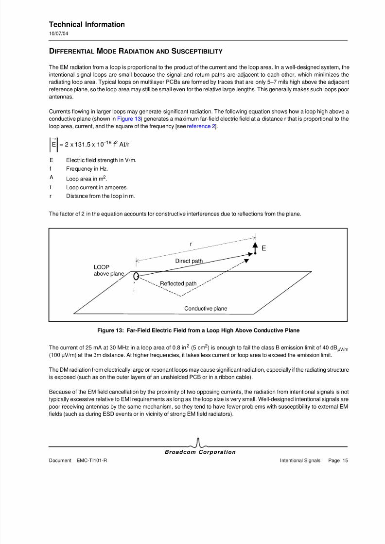
DIFFERENTIAL MODE RADIATION AND SUSCEPTIBILITY
The EM radiation from a loop is proportional to the product of the current and the loop area. In a well-designed system, the
intentional signal loops are small because the signal and return paths are adjacent to each other, which minimizes the
radiating loop area. Typical loops on multilayer PCBs are formed by traces that are only 5–7 mils high above the adjacent
reference plane, so the loop area may still be small even for the relative large lengths. This generally makes such loops poor
antennas.
Currents flowing in larger loops may generate significant radiation. The following equation shows how a loop high above a
conductive plane (shown in Figure 13) generates a maximum far-field electric field at a distance r that is proportional to the
loop area, current, and the square of the frequency [see reference 2].
The factor of 2 in the equation accounts for constructive interferences due to reflections from the plane.
Figure 13: Far-Field Electric Field from a Loop High Above Conductive Plane
The current of 25 mA at 30 MHz in a loop area of 0.8 in 2 (5 cm2) is enough to fail the class B emission limit of 40 dBµV/m
(100 µV/m) at the 3m distance. At higher frequencies, it takes less current or loop area to exceed the emission limit.
The DM radiation from electrically large or resonant loops may cause significant radiation, especially if the radiating structure
is exposed (such as on the outer layers of an unshielded PCB or in a ribbon cable).
Because of the EM field cancellation by the proximity of two opposing currents, the radiation from intentional signals is not
typically excessive relative to EMI requirements as long as the loop size is very small. Well-designed intentional signals are
poor receiving antennas by the same mechanism, so they tend to have fewer problems with susceptibility to external EM
fields (such as during ESD events or in vicinity of strong EM field radiators).
E Electric field strength in V/m.
f Frequency in Hz.
A Loop area in m2.
I Loop current in amperes.r Distance from the loop in m.
E = 2 x 131.5 x 10–16 f2 AI/r→
Conductive ground plane
Direct path
Reflected path
r E
LOOPabove plane
r
Conductive plane
LOOPabove plane
8/7/2019 Metodos_PCB
http://slidepdf.com/reader/full/metodospcb 22/54
Technical Information10/07/04
Broadcom Corporation
Page 16 Intentional Signals Document EMC-TI101-R
The EM fields generated by a poor radiator may still be relatively strong in the close proximity of the radiator, but they fall off
rapidly with the distance. The most significant potential for well-designed intentional signals to cause excessive radiation is
to couple the near field into an electrically large adjacent structure. If that structure is electrically large, it can be a cause of
secondary radiation of much stronger EM field. This may be a case when the board traces are running close to the edges
of the board in the vicinity of metal mechanical parts such as card guides or board stiffeners, or if they are close to the I/O
area on a PCB and couple with the signals that connect to the cables.
DISCONTINUITY IN THE CURRENT PATH
The most common source of increased EMI and crosstalk related to the intentional signals is a poorly designed current path,
where the current cannot flow in such a way that there is always adjacent current of the opposite direction. Poorly designed
current path does not take advantage of current cancellation (see “Currents and EM Fields” on page 3“), and does not
minimize the resulting EM field emission and coupling. The same is true for the unintentional currents, and the same
principles that govern design for the intentional signals must be considered when designing suppression of the unintentional
signals. When the minimum-area current path formed by two opposing currents flowing adjacent to each other is provided,
the EMI and crosstalk are minimized.
Routing Across a Slot in the Plane
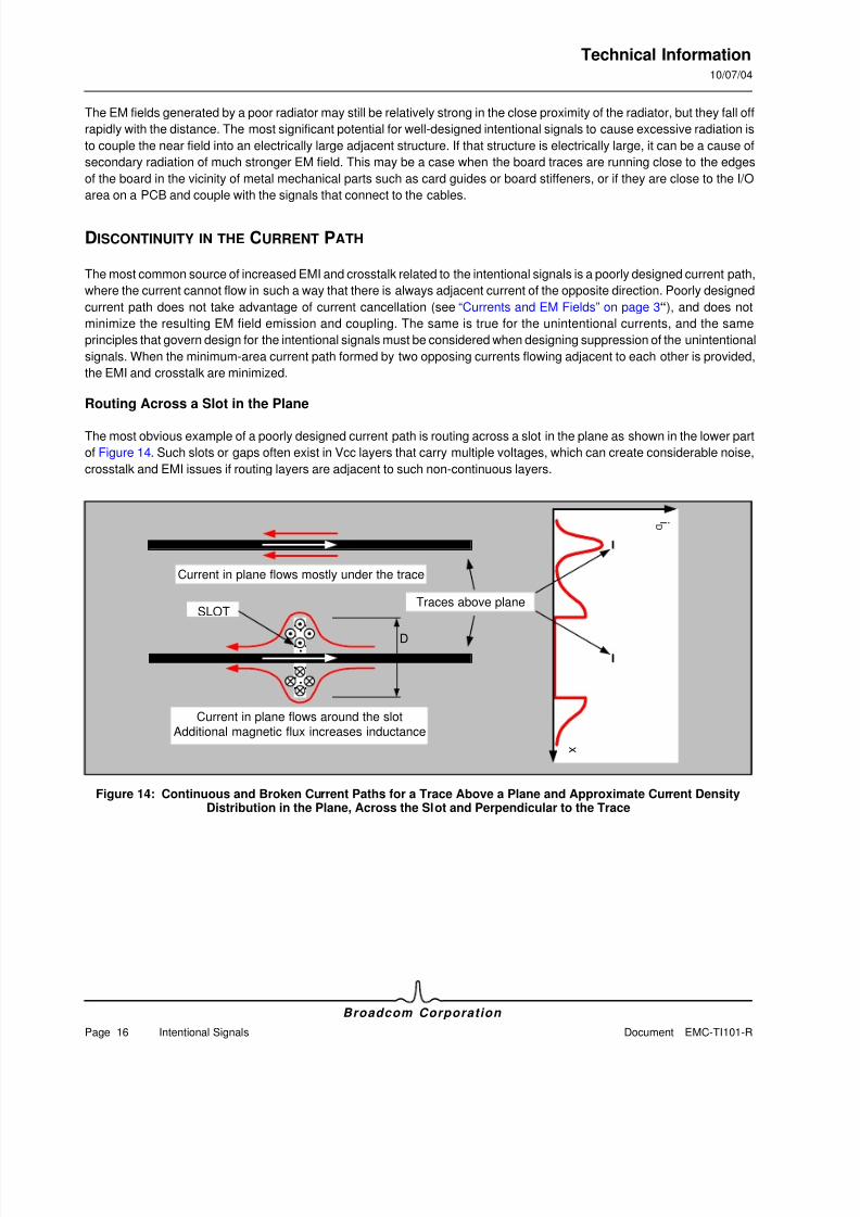
The most obvious example of a poorly designed current path is routing across a slot in the plane as shown in the lower part
of Figure 14. Such slots or gaps often exist in Vcc layers that carry multiple voltages, which can create considerable noise,
crosstalk and EMI issues if routing layers are adjacent to such non-continuous layers.
Figure 14: Continuous and Broken Current Paths for a Trace Above a Plane and Approximate Current DensityDistribution in the Plane, Across the Slot and Perpendicular to the Trace
Current in plane flows around the slot
Additional magnetic flux increases inductance
Current in plane flows mostly under the trace
i D
x
Traces above planeSLOT
D

8/7/2019 Metodos_PCB
http://slidepdf.com/reader/full/metodospcb 23/54
Technical Information10/07/04
Broadcom Corporation
Document EMC-TI101-R Intentional Signals Page 17
The current cannot cross the gap under the trace. It diverts its flow around the slot instead, because it must flow in a closed
loop. If the proper path is not provided, the current still finds a way to close the loop. Increased magnetic flux near the slot
increases inductance in the line as shown in Figure 15.
Figure 15: Model of a Transmission Line Running Across a Slot in Plane
The following shows how an approximation for the added inductance can be calculated [see reference 1].
LSLOT ≈ 5Dln(D/w)
LSLOT Inductance in series with the transmission line in nH.
D Perpendicular length of current diversion from under the trace in inches.
w Trace width in inches.
lT
g g ggc c c c
rT
Lslot
lTrT lTrT lTrT
lPrP lPrPlPrP lPrP
8/7/2019 Metodos_PCB
http://slidepdf.com/reader/full/metodospcb 24/54
Technical Information10/07/04
Broadcom Corporation
Page 18 Intentional Signals Document EMC-TI101-R
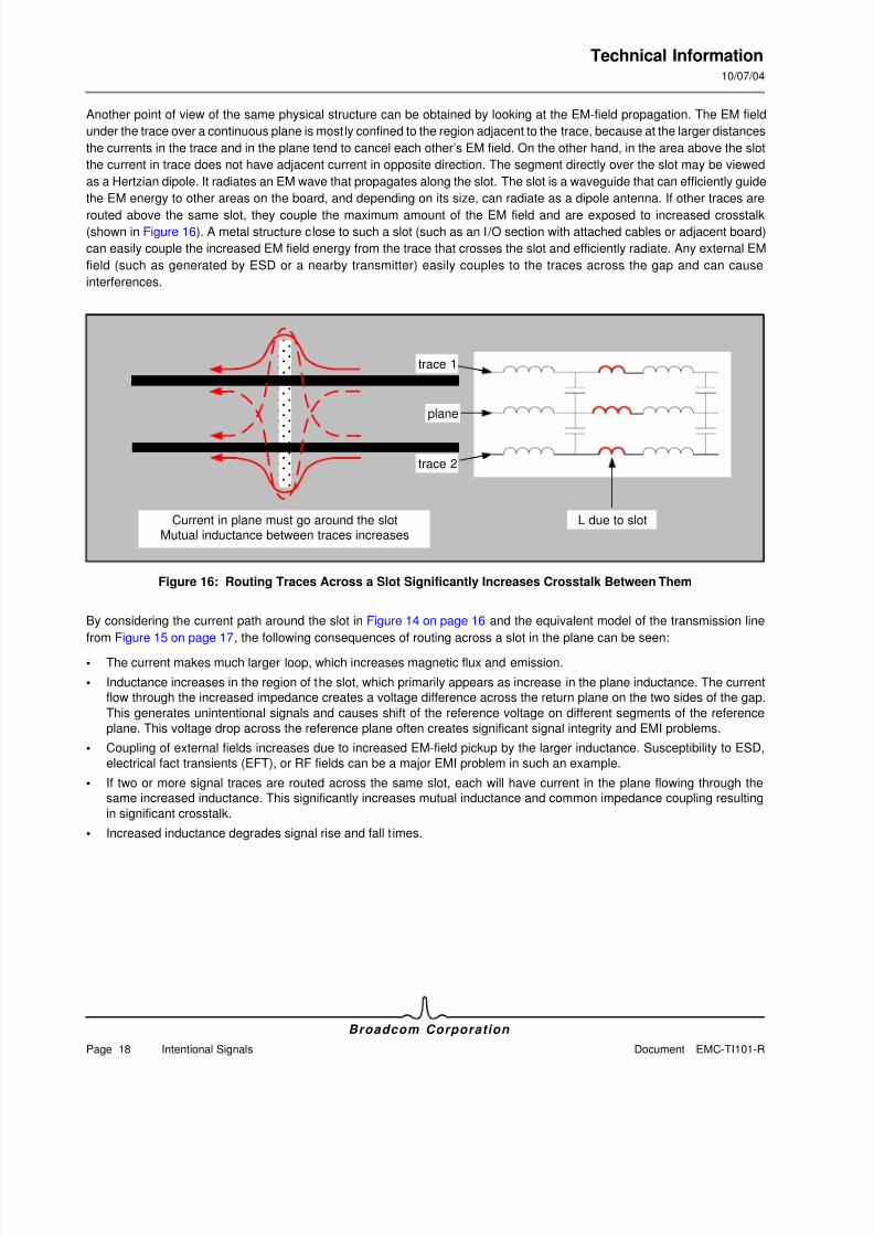
Another point of view of the same physical structure can be obtained by looking at the EM-field propagation. The EM field
under the trace over a continuous plane is mostly confined to the region adjacent to the trace, because at the larger distances
the currents in the trace and in the plane tend to cancel each other’s EM field. On the other hand, in the area above the slot
the current in trace does not have adjacent current in opposite direction. The segment directly over the slot may be viewed
as a Hertzian dipole. It radiates an EM wave that propagates along the slot. The slot is a waveguide that can efficiently guide
the EM energy to other areas on the board, and depending on its size, can radiate as a dipole antenna. If other traces are
routed above the same slot, they couple the maximum amount of the EM field and are exposed to increased crosstalk(shown in Figure 16). A metal structure close to such a slot (such as an I/O section with attached cables or adjacent board)
can easily couple the increased EM field energy from the trace that crosses the slot and efficiently radiate. Any external EM
field (such as generated by ESD or a nearby transmitter) easily couples to the traces across the gap and can cause
interferences.
Figure 16: Routing Traces Across a Slot Significantly Increases Crosstalk Between Them
By considering the current path around the slot in Figure 14 on page 16 and the equivalent model of the transmission line
from Figure 15 on page 17, the following consequences of routing across a slot in the plane can be seen:
• The current makes much larger loop, which increases magnetic flux and emission.
• Inductance increases in the region of the slot, which primarily appears as increase in the plane inductance. The current
flow through the increased impedance creates a voltage difference across the return plane on the two sides of the gap.
This generates unintentional signals and causes shift of the reference voltage on different segments of the reference
plane. This voltage drop across the reference plane often creates significant signal integrity and EMI problems.
• Coupling of external fields increases due to increased EM-field pickup by the larger inductance. Susceptibility to ESD,
electrical fact transients (EFT), or RF fields can be a major EMI problem in such an example.
• If two or more signal traces are routed across the same slot, each will have current in the plane flowing through the
same increased inductance. This significantly increases mutual inductance and common impedance coupling resulting
in significant crosstalk.
• Increased inductance degrades signal rise and fall t imes.
Current in plane must go around the slotMutual inductance between traces increases
plane
trace 1
trace 2
L due to slot
8/7/2019 Metodos_PCB
http://slidepdf.com/reader/full/metodospcb 25/54
Technical Information10/07/04
Broadcom Corporation
Document EMC-TI101-R Intentional Signals Page 19
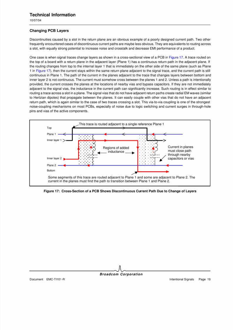
Changing PCB Layers
Discontinuities caused by a slot in the return plane are an obvious example of a poorly designed current path. Two other
frequently encountered cases of discontinuous current paths are maybe less obvious. They are equivalents to routing across
a slot, with equally strong potential to increase noise and crosstalk and decrease EMI performance of a product.
One case is when signal traces change layers as shown in a cross-sectional view of a PCB in Figure 17. A trace routed onthe top of a board with a return plane in the adjacent layer (Plane 1) has a continuous return path in the adjacent plane. If
the routing changes from top to the internal layer 1 that is immediately on the other side of the same plane (such as Plane
1 in Figure 17), then the current stays within the same return plane adjacent to the signal trace, and the current path is still
continuous in Plane 1. The path of the current in the planes adjacent to the trace that changes layers between bottom and
inner layer 2 is not continuous. The current must somehow cross between the planes 1 and 2. Unless a path is intentionally
provided, the current crosses the planes at the locations of nearby vias and bypass capacitors. If they are not immediately
adjacent to the signal vias, the inductance in the current path can significantly increase. Such routing is in effect similar to
routing a trace across a slot in a plane. The signal vias that do not have adjacent return paths create radial EM waves (similar
to Hertzian dipoles) that propagate between the planes. It can easily couple with other vias that do not have an adjacent
return path, which is again similar to the case of two traces crossing a slot. This via-to-via coupling is one of the strongest
noise-coupling mechanisms on most PCBs, especially of noise due to logic switching and current surges in through-hole
pins and vias of the active components.
Figure 17: Cross-Section of a PCB Shows Discontinuous Current Path Due to Change of Layers
Current in planesmust close paththrough nearbycapacitors or vias
Regions of addedinductance
This trace is routed adjacent to a single reference Plane 1
Some segments of this trace are routed adjacent to Plane 1, and some are adjacentto Plane 2. The current in the planes must hop between Plane1 and Plane2.
Top
Bottom
Plane 1
Plane 2
Inner layer 1
Inner layer 2
Some segments of this trace are routed adjacent to Plane 1 and some are adjacent to Plane 2. Thecurrent in the planes must find the path to transition between Plane 1 and Plane 2.
8/7/2019 Metodos_PCB
http://slidepdf.com/reader/full/metodospcb 26/54
Technical Information10/07/04
Broadcom Corporation
Page 20 Intentional Signals Document EMC-TI101-R
Even if the nearby vias or capacitors are relatively close to the signal transition, they add impedance in the return path. It is
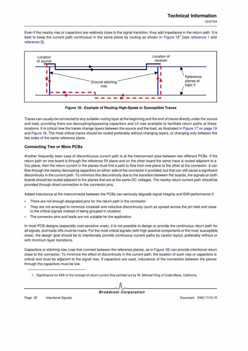
best to keep the current path continuous in the same plane by routing as shown in Figure 181 [see reference 1 and
reference 3].
Figure 18: Example of Routing High-Speed or Susceptible Traces
Traces can usually be connected to any suitable routing layer at the beginning and the end of traces directly under the source
and load, providing there are decoupling/bypassing capacitors and L0 vias available to facilitate return paths at these
locations. It is critical how the traces change layers between the source and the load, as illustrated in Figure 17 on page 19
and Figure 18. The most critical traces should be routed preferably without changing layers, or changing only between the
two sides of the same reference plane.
Connecting Two or More PCBs
Another frequently seen case of discontinuous current path is at the interconnect area between two different PCBs. If the
return path on one board is through the reference 0V plane and on the other board the same trace is routed adjacent to a
Vcc plane, then the return current in the planes must find a path to flow from one plane to the other at the connector. It can
flow through the nearby decoupling capacitors on either side of the connector if provided, but that can still cause a significant
discontinuity in the current path. To minimize this discontinuity due to the transition between the boards, the signals on both
boards should be routed adjacent to the planes that are at the same DC voltages. The nearby return current path should beprovided through direct connection in the connector pins.
Added inductance at the interconnects between the PCBs can seriously degrade signal integrity and EMI performance if:
• There are not enough designated pins for the return path in the connector
• They are not arranged to minimize crosstalk and inductive discontinuity (such as spread across the pin field and close
to the critical signals instead of being grouped in clusters)
• The connector pins and leads are not suitable for the application
In most PCB designs (especially cost-sensitive ones), it is not possible to design or provide the continuous return path for
all signals, and trade-offs must be made. For the most critical signals (with high spectral components or the most susceptible
ones), the design goal should be to intentionally provide continuous current paths by careful layout, preferably without or
with minimum layer transitions.
Capacitors or stitching vias (vias that connect between the reference planes, as in Figure 18) can provide intentional return
close to the connector. To minimize the effect of discontinuity in the current path, the location of such vias or capacitors is
critical and must be adjacent to the signal vias. If capacitors are used, inductance of the connection between the planes
through the capacitors must be low.
1. Significance for EMI of the concept of return current flow pointed out by W. Michael King of Costa Mesa, California.
Location
of source
Referenceplanes atlogic 0
Ground stitchingvias
Location of
receiver
8/7/2019 Metodos_PCB
http://slidepdf.com/reader/full/metodospcb 27/54
Technical Information10/07/04
Broadcom Corporation
Document EMC-TI101-R Intentional Signals Page 21
EDGES OF THE PLANES
Traces Close to the Edges of the Planes
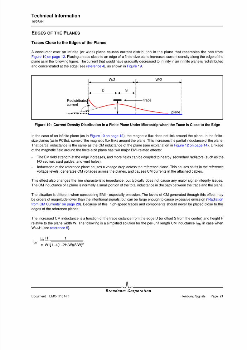
A conductor over an infinite (or wide) plane causes current distribution in the plane that resembles the one from
Figure 10 on page 12. Placing a trace close to an edge of a finite-size plane increases current density along the edge of the
plane as in the following figure. The current that would have gradually decreased to infinity in an infinite plane is redistributed
and concentrated at the edge [see reference 4], as shown in Figure 19.
Figure 19: Current Density Distribution in a Finite Plane Under Microstrip when the Trace is Close to the Edge
In the case of an infinite plane (as in Figure 10 on page 12), the magnetic flux does not link around the plane. In the finite-
size planes (as in PCBs), some of the magnetic flux links around the plane. This increases the partial inductance of the plane.
That partial inductance is the same as the CM inductance of the plane (see explanation in Figure 12 on page 14). Linkage
of the magnetic field around the finite-size plane has two major EMI-related effects:
• The EM field strength at the edge increases, and more fields can be coupled to nearby secondary radiators (such as the
I/O section, card guides, and vent holes).
• Inductance of the reference plane causes a voltage drop across the reference plane. This causes shifts in the reference
voltage levels, generates CM voltages across the planes, and causes CM currents in the attached cables.
This effect also changes the line characteristic impedance, but typically does not cause any major signal-integrity issues.The CM inductance of a plane is normally a small portion of the total inductance in the path between the trace and the plane.
The situation is different when considering EMI - especially emission. The levels of CM generated through this effect may
be orders of magnitude lower than the intentional signals, but can be large enough to cause excessive emission (“Radiation
from CM Currents” on page 28). Because of this, high-speed traces and components should never be placed close to the
edges of the reference planes.
The increased CM inductance is a function of the trace distance from the edge D (or offset S from the center) and height H
relative to the plane width W. The following is a simplified solution for the per-unit length CM inductance l CM in case when
W>>H [see reference 5].
W/2 W/2
D S
H
trace
plane
Re-distributedcurrent
Redistributedcurrent
1
1–4(1–2H/W)(S/W)2
H
π W
µ0
lCM=
8/7/2019 Metodos_PCB
http://slidepdf.com/reader/full/metodospcb 28/54
Technical Information10/07/04
Broadcom Corporation
Page 22 Intentional Signals Document EMC-TI101-R
The important result is that the lCM is fairly constant over the wide range of S/W, but it increases significantly as the trace
approaches the edge. The maximum increase of the lCM relative to a trace in the center of the plane is when S=W/2 (i.e.,
when the trace is directly at the edge):
Because the radiated electric field strength E is proportional to the CM voltage, it is also proportional to the CM impedance
(inductance). The maximum relative difference in emission∆dBmaxE from a trace in the center and a trace at the edge can
be calculated as:
A model for the worst-case radiation due to CM inductance of the plane is a dipole antenna attached to the CM voltage
source (shown in Figure 20). The DM current in the CM inductance induces the CM voltage of VCM, which feeds the dipole.This model also illustrates why it is not a good practice to place connectors and cables on the opposite sides of a PCB.
Figure 20: Dipole Model of Radiation Due to CM Impedance of a Plane
lCM (S/W=0.5) W
lCM (S/W=0) 2H (for H= constant)≈
∆dBmaxE ≈ 20 log( )≈ 10 log( )–3
W W
2H H
Plane
IDM
Attached cables form a dipole antenna
LCM
= 0
DM Currnt IDM (including power switching and surges) generates VCM on the impedance of the plane.
VCM
is the source of CM current ICM
and radiation from the attached cables
VCM
= -LCM
dIDM
dt
IDM
LCMICM
ICM

8/7/2019 Metodos_PCB
http://slidepdf.com/reader/full/metodospcb 29/54
Technical Information10/07/04
Broadcom Corporation
Document EMC-TI101-R Intentional Signals Page 23
An often used rule of thumb is to space the traces a certain distance away from the edges of the planes, where the distance
is related to the dielectric thickness H between the trace and the nearest plane-layer. The radiated electric field strength E
is a function of the relative geometry of the trace and plane, the DM (intentional) current IDM in the trace and the plane, and
the attached antenna (cable) that is driven by the CM voltage developed over the total CM inductance LCM. A more exact
relation for the required distance from the edge should take into account the board and the trace geometry, current, and
radiation model. Assuming a dipole model from Figure 20 on page 22, it is possible to find the maximum acceptable LCM MAX
for the field strength E at the distance r under worst-case conditions.
The minimum distance from a trace to the edge that does not cause worst-case radiation above a given E field strength can
be found from the given expressions.
EM Field Propagation at the Edges of the Planes
Another mechanism of radiation is related to the EM field propagation between the PCB planes and its fringing at the edges.
The PCB planes are low-impedance parallel-plane transmission lines. Signal and power supply vias and through-hole pins
can be approximated by the Hertzian dipoles, which generate radial EM waves that propagate between the planes. When
the EM waves reach the board edges, a part of the field reflects and a part propagates to the outside because of the
impedance discontinuity at the board edge. If there is no low-impedance connection between the planes at the edge, then
the voltage between the planes at the discontinuity is increased due to transition from low impedance between the planes
to high impedance (free space) medium. In addition and similarly to the example with a trace close to the edge, the magnetic
field that links around the edge causes the plane partial inductance to increase. Intentional currents (signal and power
supply) through the increased inductance cause CM voltage across the plane and radiated emission from the attached
wiring.
The electrical size of PCB cross-sections is small. The field strength rapidly decreases with the distance from the edge, and
direct radiation from the edge is rarely a problem. If there is any electrically large metal structure adjacent to the board edge
(such as a cable, wire, seam or a PCB guide in a chassis), the fringing EM field can couple RF energy into this structure.
This electrically large structure may then radiate efficiently and cause emission problems.
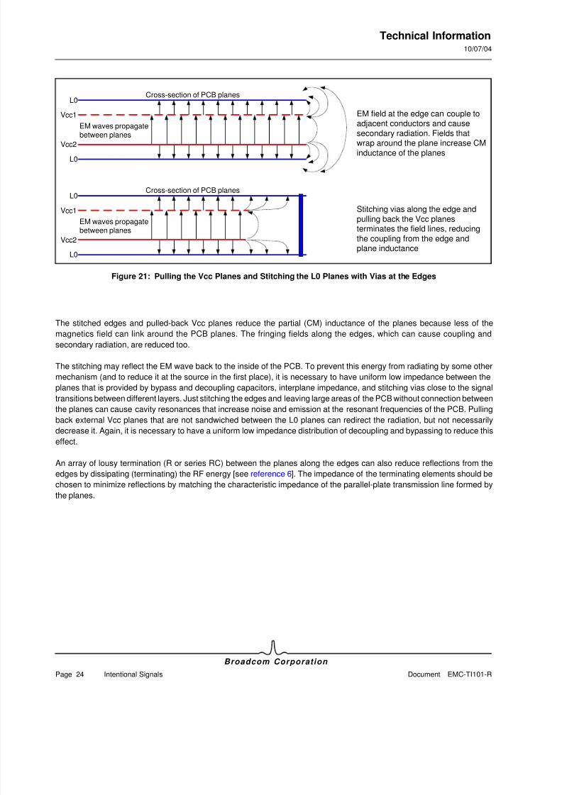
When the Vcc planes are sandwiched between the L0 planes, the fringing EM fields can be decreased by reducing the size
of the Vcc planes, pulling the L0 planes’ edges back, and adding vias (or capacitors) at the edges of the planes shown in
the following Figure 21 on page 24 [see reference 3].
LCM MAX < E73
60
r
ω IDMl
0.2 E r~
f IDMl
f = frequencyl = length of traceIDM = DM current in trace
r = distance
8/7/2019 Metodos_PCB
http://slidepdf.com/reader/full/metodospcb 30/54
Technical Information10/07/04
Broadcom Corporation
Page 24 Intentional Signals Document EMC-TI101-R
Figure 21: Pulling the Vcc Planes and Stitching the L0 Planes with Vias at the Edges
The stitched edges and pulled-back Vcc planes reduce the partial (CM) inductance of the planes because less of the
magnetics field can link around the PCB planes. The fringing fields along the edges, which can cause coupling and
secondary radiation, are reduced too.
The stitching may reflect the EM wave back to the inside of the PCB. To prevent this energy from radiating by some other
mechanism (and to reduce it at the source in the first place), it is necessary to have uniform low impedance between the
planes that is provided by bypass and decoupling capacitors, interplane impedance, and stitching vias close to the signal
transitions between different layers. Just stitching the edges and leaving large areas of the PCB without connection between
the planes can cause cavity resonances that increase noise and emission at the resonant frequencies of the PCB. Pullingback external Vcc planes that are not sandwiched between the L0 planes can redirect the radiation, but not necessarily
decrease it. Again, it is necessary to have a uniform low impedance distribution of decoupling and bypassing to reduce this
effect.
An array of lousy termination (R or series RC) between the planes along the edges can also reduce reflections from the
edges by dissipating (terminating) the RF energy [see reference 6]. The impedance of the terminating elements should be
chosen to minimize reflections by matching the characteristic impedance of the parallel-plate transmission line formed by
the planes.
EM waves propagatebetween planes
Cross-section of PCB planesL0
L0
Vcc1
Vcc2
Cross-section of PCB planes
EM waves propagate
between planes
L0
L0
Vcc1
Vcc2
Stitching vias along the edge andpulling back the Vcc planesterminates the field lines, reducingthe coupling from the edge andplane inductance
EM field at the edge can couple toadjacent conductors and cause
secondary radiation. Fields thatwrap around the plane increase CMinductance of the planes
8/7/2019 Metodos_PCB
http://slidepdf.com/reader/full/metodospcb 31/54
Technical Information10/07/04
Broadcom Corporation
Document EMC-TI101-R Unintentional Currents and Voltages Page 25
UNINTENTIONAL CURRENTS AND VOLTAGES
COMMON MODE VOLTAGE AND CURRENT
Sources
The CM currents are the primary sources of emission from electronic devices, so it is important to understand what they are,
how they are generated, and how to suppress them. The CM currents originate due to imperfect, non-zero impedance (due
to skin effect and inductance) of the current paths (especially in the reference conductors). They are also caused by coupling
(crosstalk) and imbalances in circuits, electrical signals, and routing. The CM currents can be superimposed to the DM
currents, flow in the system return traces, planes, and chassis, and do not necessarily follow the intended path of the
designed DM signal currents. The CM currents take much larger loops and their path is often completed through the chassis,
I/O cables, or system environment outside of the chassis. It will be shown why CM currents radiate more than DM currents,
and that the same design considerations for continuous current path with opposing currents adjacent to each other (as
discussed in “Currents and EM Fields” on page 3 and “Discontinuity in the Current Path” on page 16) must be applied to CM
currents as well for efficient EMI design.
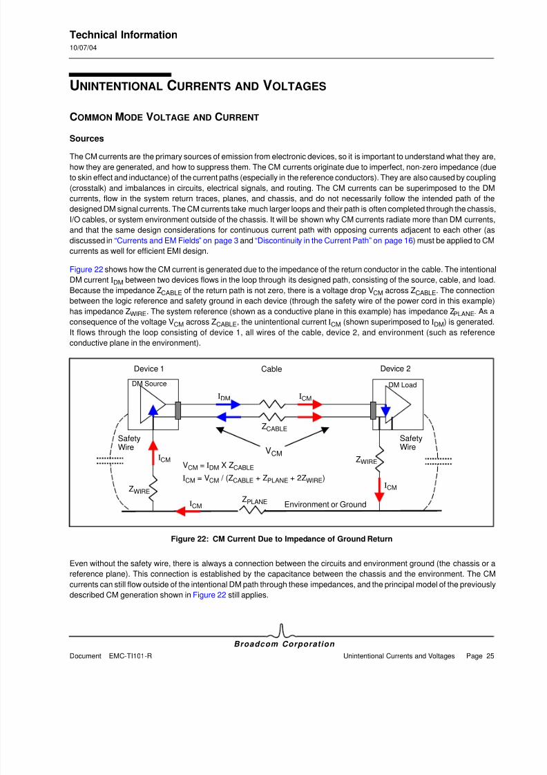
Figure 22 shows how the CM current is generated due to the impedance of the return conductor in the cable. The intentionalDM current IDM between two devices flows in the loop through its designed path, consisting of the source, cable, and load.
Because the impedance ZCABLE of the return path is not zero, there is a voltage drop VCM across ZCABLE. The connection
between the logic reference and safety ground in each device (through the safety wire of the power cord in this example)
has impedance ZWIRE. The system reference (shown as a conductive plane in this example) has impedance ZPLANE. As a
consequence of the voltage VCM across ZCABLE, the unintentional current ICM (shown superimposed to IDM) is generated.
It flows through the loop consisting of device 1, all wires of the cable, device 2, and environment (such as reference
conductive plane in the environment).
Figure 22: CM Current Due to Impedance of Ground Return
Even without the safety wire, there is always a connection between the circuits and environment ground (the chassis or a
reference plane). This connection is established by the capacitance between the chassis and the environment. The CM
currents can still flow outside of the intentional DM path through these impedances, and the principal model of the previously
described CM generation shown in Figure 22 still applies.
CableDevice 1 Device 2
DM Source
IDM
ICM
ZCABLE
VCM
DM Load
VCM = IDM X ZCABLE
ICM = VCM / (ZCABLE + ZPLANE + 2ZWIRE)
SafetyWire
SafetyWire
ICM
Environment or Ground
ZWIRE
ICM
ICMZPLANE
ZWIRE
8/7/2019 Metodos_PCB
http://slidepdf.com/reader/full/metodospcb 32/54
Technical Information10/07/04
Broadcom Corporation
Page 26 Unintentional Currents and Voltages Document EMC-TI101-R
The ICM can be generated by the same mechanism on the PCB level or in the IC package, when the impedance of the return
path is significant, such as from:
• Inductance of the PCB reference planes
• Inductance of the component power supply leads and paths
In each case, the intended signals cause voltage drops across these impedances, and there is a difference in voltage levelson each side of the common impedance (e.g. ZCABLE and ZWIRE in Figure 22 on page 25) as a consequence. This is usually
referred to as ground bounce or power bounce , which can happen at all levels of a device from the silicon die, through the
IC package, PCB structures, and intra-system and inter-system cables and connectors.
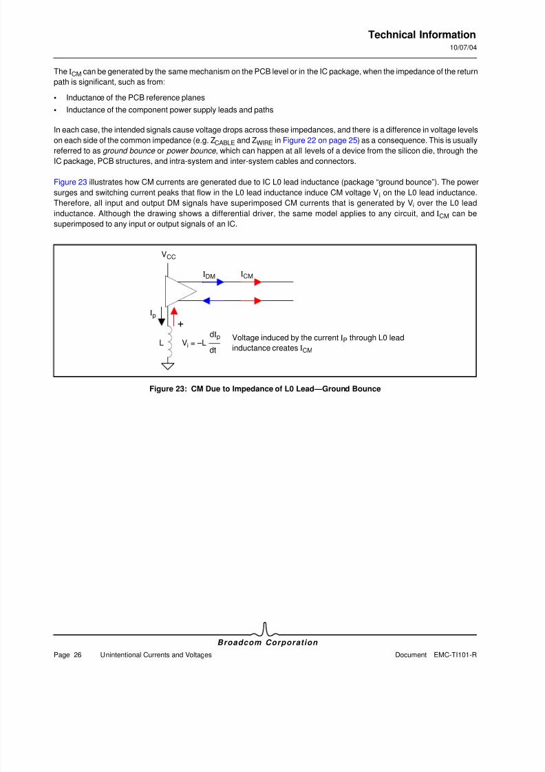
Figure 23 illustrates how CM currents are generated due to IC L0 lead inductance (package “ground bounce”). The power
surges and switching current peaks that flow in the L0 lead inductance induce CM voltage V i on the L0 lead inductance.
Therefore, all input and output DM signals have superimposed CM currents that is generated by V i over the L0 lead
inductance. Although the drawing shows a differential driver, the same model applies to any circuit, and ICM can be
superimposed to any input or output signals of an IC.
Figure 23: CM Due to Impedance of L0 Lead—Ground Bounce
+
VCC
IDM ICM
Ip
LdIp
Vi = –LVoltage induced by the current IP through L0 lead
inductance creates ICMdt
8/7/2019 Metodos_PCB
http://slidepdf.com/reader/full/metodospcb 33/54
Technical Information10/07/04
Broadcom Corporation
Document EMC-TI101-R Unintentional Currents and Voltages Page 27
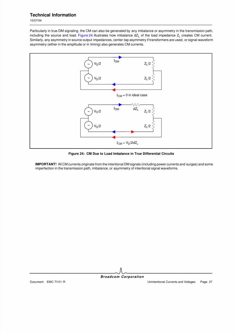
Particularly in true-DM signaling, the CM can also be generated by any imbalance or asymmetry in the transmission path,
including the source and load. Figure 24 illustrates how imbalance dZL of the load impedance ZL creates CM current.
Similarly, any asymmetry in source output impedances, center-tap asymmetry if transformers are used, or signal-waveform
asymmetry (either in the amplitude or in timing) also generates CM currents.
Figure 24: CM Due to Load Imbalance in True Differential Circuits
IMPORTANT! All CM currents originate from the intentional DM signals (including power currents and surges) and someimperfection in the transmission path, imbalance, or asymmetry of intentional signal waveforms.
ICM = VD/2dZL
~
~
~
~
ICM = 0 in ideal case
IDMVD/2 ZL/2
ZL/2VD/2
IDMVD/2 ZL/2
ZL/2VD/2
dZL
8/7/2019 Metodos_PCB
http://slidepdf.com/reader/full/metodospcb 34/54
Technical Information10/07/04
Broadcom Corporation
Page 28 Unintentional Currents and Voltages Document EMC-TI101-R
Radiation from CM Currents
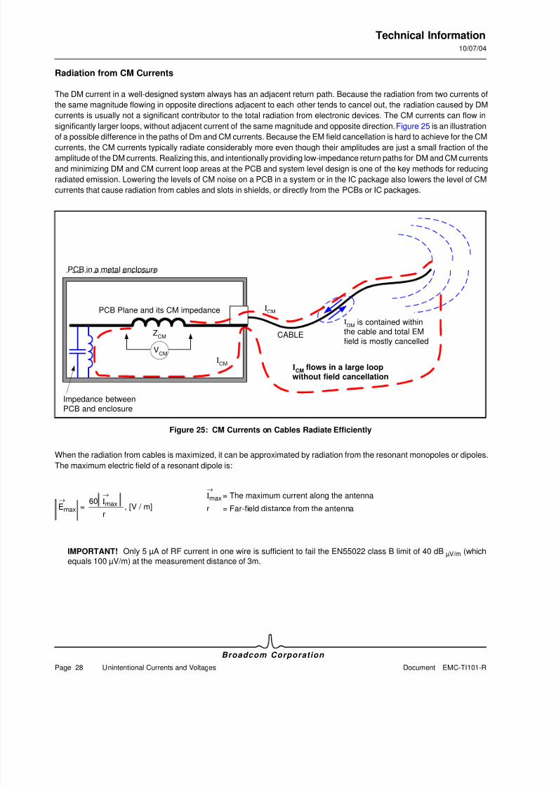
The DM current in a well-designed system always has an adjacent return path. Because the radiation from two currents of
the same magnitude flowing in opposite directions adjacent to each other tends to cancel out, the radiation caused by DM
currents is usually not a significant contributor to the total radiation from electronic devices. The CM currents can flow in
significantly larger loops, without adjacent current of the same magnitude and opposite direction. Figure 25 is an illustration
of a possible difference in the paths of Dm and CM currents. Because the EM field cancellation is hard to achieve for the CMcurrents, the CM currents typically radiate considerably more even though their amplitudes are just a small fraction of the
amplitude of the DM currents. Realizing this, and intentionally providing low-impedance return paths for DM and CM currents
and minimizing DM and CM current loop areas at the PCB and system level design is one of the key methods for reducing
radiated emission. Lowering the levels of CM noise on a PCB in a system or in the IC package also lowers the level of CM
currents that cause radiation from cables and slots in shields, or directly from the PCBs or IC packages.
Figure 25: CM Currents on Cables Radiate Efficiently
When the radiation from cables is maximized, it can be approximated by radiation from the resonant monopoles or dipoles.
The maximum electric field of a resonant dipole is:
IMPORTANT! Only 5 µA of RF current in one wire is sufficient to fail the EN55022 class B limit of 40 dB µV/m (which
equals 100 µV/m) at the measurement distance of 3m.
Impedance between
PCB and enclosure
CABLE
IDM
is contained withinthe cable and total EM
field is mostly cancelled
ICM
flows in a large loopwithout field cancellation
PCB Plane and its CM impedance
ZCM
VCM
PCB in a metal anclosure
ICM
ICM
PCB in a metal enclosure
Emax = , [V / m]→ 60 Imax
r
→ Imax = The maximum current along the antenna
r = Far-field distance from the antenna
→
8/7/2019 Metodos_PCB
http://slidepdf.com/reader/full/metodospcb 35/54
Technical Information10/07/04
Broadcom Corporation
Document EMC-TI101-R Unintentional Currents and Voltages Page 29
Reducing Emission from CM Currents
Reducing emission from CM currents follows the same basic principles as reducing emission from any currents, which is
essentially control of the signal spectrum, amplitude, impedance of the current path, minimizing the loop area, and/or the
effectiveness of the radiating elements.
• Because the CM currents originate from DM currents, they have the same spectral components and their amplitudesare related. Reducing the amplitude and the unwanted spectral components of DM currents by changing the intentional
signal voltage spectrum reduces the same components of CM currents. It can be achieved by e.g., filtering at the
source or not using faster logic families than needed.
• The CM currents are generated by DM currents flowing through non-zero impedance in their return path. Some
measures to reduce the impedance of the return path are providing wide, solid (not perforated), continuous reference
planes, as well as routing signals close to the reference and away from the edges of the planes. This reduces CM
voltage and CM currents and applies to all intentional current return paths, whether or not they are at L0 or Vcc levels.
• The first two bullets show how to reduce CM voltage to reduce CM current. The amplitude of CM currents can also be
reduced by increasing the impedance in the CM current path (such as by using CM chokes in the path of CM currents),
and also by reducing the amplitude of the intentional DM currents (e.g., using series termination resistors at the source).
• The ICM can radiate much more than IDM (often a couple of orders of magnitude), because there is no adjacent return-
current path for ICM. Emission from ICM can be reduced by intentionally providing adjacent return paths for ICM, which
results in field cancellation and much smaller loop and lower return path impedance for ICM
. For example, internal
cabling in a system can be arranged in such a way that it is adjacent to the chassis, which is the return path for CM
currents within a metal enclosure.
The same considerations about the unbroken return path, close coupling between the currents in traces and return
planes and traces, and low impedance of the return path (which apply to the intentional DM currents) also apply to the
CM currents.
• This last bullet is one of the major factors to consider when designing a metal enclosure (chassis) and providing (or not)
intentional contacts between the PCB and the chassis.
CROSSTALK
Crosstalk is always a result of mutual impedances between two or more circuits. Crosstalk from the coupling between traces
across a gap or between vias when PCB traces change layers has already been discussed in the context of discontinuouscurrent path (see “Discontinuity in the Current Path” on page 16). The crosstalk can be:
• Capacitive, between two or more traces, determined by the proximity and the surface area of coupled circuits/traces
• Inductive, due to the linkage of the magnetic flux between two current loops and the related mutual inductance.
Distance and the area of the current loops determine the amount of inductive coupling.
• Common-impedance, resulting from impedances in series with the common current path. An example of the common-
impedance coupling is two signals flowing through a common inductance such as L0 lead or a slot in a reference plane.
A voltage drop over the common impedance caused by one current modulates the other circuit and appears as coupled
noise in the other circuit.
The DM crosstalk is often evaluated as a part of the functional analysis of circuits, but crosstalk is rarely well analyzed from
the EMI point of view, especially the CM crosstalk. Even though it may not cause any significant functional problem, low
levels of crosstalk can cause emission failures if coupled to the I/O lines. It was previously shown in Figure 25 on page 28,
that about 5 µA on one wire may be enough to exceed the emission limits. This level can easily couple from signal traces
(especially from high-speed signals) and radiate if a trace is located close to the I/O section. Static traces (such as LED
traces) do not carry intentional high-speed signals, but usually carry unintentionally coupled high-frequency currents and
voltages. Crosstalk between such traces and the I/O traces may cause major emission problems. The DM-to-CM and CM-
to-CM crosstalk follows the same principles as DM-to-DM crosstalk. For EMI analysis, the CM crosstalk (such as trace-to-
trace, plane-to-trace, or plane-to-plane) should also be considered.

8/7/2019 Metodos_PCB
http://slidepdf.com/reader/full/metodospcb 36/54
Technical Information10/07/04
Broadcom Corporation
Page 30 Unintentional Currents and Voltages Document EMC-TI101-R
Crosstalk between two traces on the same layer follows the same dependence on the height above the plane and distance
from the traces as the distribution of current density in the plane under the traces (see Figure 10 on page 12).
Crosstalk decreases inversely proportionally to the square of distance and increases with the square of height. Minimizing
crosstalk reduces emission and increases immunity and noise margin. Usually a compromise must be made between the
sometimes opposing requirements for crosstalk, trace characteristic impedance, and routing density on a PCB.
Effective ways to minimize crosstalk are:
• Using short traces
• Keeping large separation between traces (especially from the I/O area) and using planes between signals
• Routing close to the signal return (e.g., low dielectric height between the traces and the L0 or Vcc plane)
• Providing a wide and continuous low-impedance return path, especially for all high-speed and I/O signals. This also
includes the return path for CM currents in cases when differential signaling is used.
• Routing signals perpendicular to each other on adjacent routing layers.
• Using series terminating resistors to terminate backward crosstalk and reduce ringing due to reflections.
Crosstalk is a form of EMI, thus the same measures decrease EMI as well.
SWITCHING NOISE BETWEEN VCC AND L0 PLANES
High-frequency noise between the Vcc and L0 planes originates from switching current passing through the power supply
pins, signal vias, and impedance of the PCB power distribution system. Pins and vias are sources of radial waves between
the planes, like the Hertzian dipoles, which cause induced RF currents and voltages on the planes. Switching currents cause
voltage drop on the plane impedance and RF voltages (noise) across the planes. When the reference planes have RF
voltage (‘ripple”) superimposed to their DC levels, all circuits will also have these RF voltages superimposed to the signals.
This increases DM and CM noise on the PCBs, and reduces noise merging on all signals.
The factors that increase the impedance of the planes are:
• Inductance due to distance (dielectric thickness) between the planes
• Holes (slots, aperture arrays)
• Edges of the planes
• Skin-effect resistance
Decoupling and bypassing capacitors can provide low impedance to minimize the RF voltages between the planes. A part
of the total impedance between the planes also comes from the planes themselves, which form a parallel-plane transmissionline with mutual capacitance and inductance. The characteristic impedance of the parallel-plate line depends on dielectric
properties and the distance between the planes. The discrete capacitors determine the low-frequency impedance between
the planes, typically up to tens of MHz. The interplane capacitance and inductance are the critical part of the total impedance
at the higher frequencies, typically starting at about a hundred or at couple of hundred MHz. Low impedance between the
planes helps keeping the RF currents localized near the source (e.g. Vcc and L0 pins of the switching digital devices) and
under the transmission lines, and preventing them from spreading throughout the board and system.
K = Crosstalk coefficient
H = Height of the trace above the reference plane
D = Center-to-center distance between the traces
crosstalk∼K
1 + D2 / H2[see reference 1]
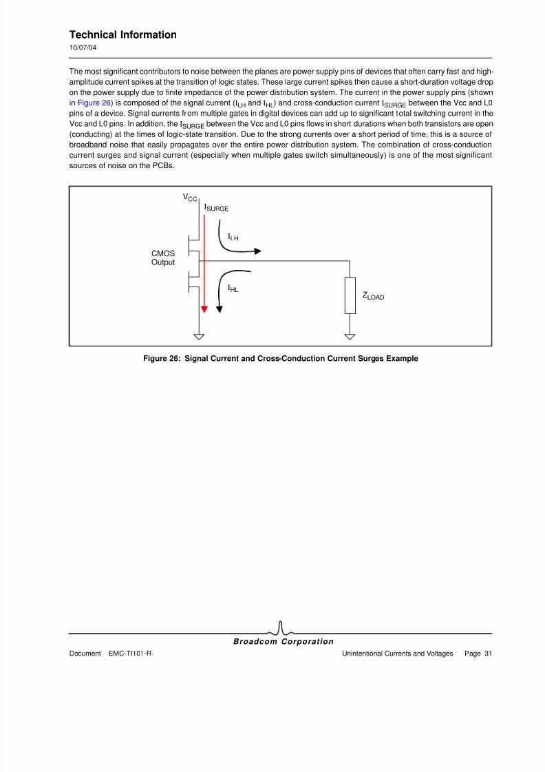
8/7/2019 Metodos_PCB
http://slidepdf.com/reader/full/metodospcb 37/54
Technical Information10/07/04
Broadcom Corporation
Document EMC-TI101-R Unintentional Currents and Voltages Page 31
The most significant contributors to noise between the planes are power supply pins of devices that often carry fast and high-
amplitude current spikes at the transition of logic states. These large current spikes then cause a short-duration voltage drop
on the power supply due to finite impedance of the power distribution system. The current in the power supply pins (shown
in Figure 26) is composed of the signal current (ILH and IHL) and cross-conduction current ISURGE between the Vcc and L0
pins of a device. Signal currents from multiple gates in digital devices can add up to significant total switching current in the
Vcc and L0 pins. In addition, the ISURGE between the Vcc and L0 pins flows in short durations when both transistors are open
(conducting) at the times of logic-state transition. Due to the strong currents over a short period of time, this is a source ofbroadband noise that easily propagates over the entire power distribution system. The combination of cross-conduction
current surges and signal current (especially when multiple gates switch simultaneously) is one of the most significant
sources of noise on the PCBs.
Figure 26: Signal Current and Cross-Conduction Current Surges Example
VCC
ILH
ZLOAD
CMOS
Output
IHL
ISURGE
8/7/2019 Metodos_PCB
http://slidepdf.com/reader/full/metodospcb 38/54
Technical Information10/07/04
Broadcom Corporation
Page 32 Unintentional Currents and Voltages Document EMC-TI101-R
One effective measure to decrease noise propagation on a PCB is filtering the power supply of high-bandwidth components
with ferrite beads and capacitors, which is typically done with the PLL and clock devices. This protects the rest of the power
distribution on the PCB from the noise generated in these circuit’s Vcc and L0 pins. Figure 27 shows an example and
measured relative amplitude of the noise voltage on the two sides of a ferrite bead. The capacitor on the V CC side of the
ferrite bead enhances the filtering performance. In the case of PLL circuits (which are also susceptible to the low frequency
power supply noise), the same filter can filter the power supply for the PLL. With this technique, it is important to provide
sufficient decoupling on the Local Vcc for proper operation of the device.
IMPORTANT! A high-impedance gap between the Vcc and the Local Vcc is formed by insertion of the ferrite bead. This
can create discontinuity in the return-current path if the clock signals are routed adjacent to the Vcc plane and across
such a gap. Such discontinuity can create serious EMI and functional crosstalk issues. Because the ferrite bead may
present an inappropriate discontinuity in the return path of signals that may flow in the Vcc planes, caution is required
when using this technique. Careful consideration of the current paths as well as of decoupling and bypassing is needed.
Figure 27: Ferrite Beads in Power Supply of Noisy Components Attenuate Noise Propagation on PCB
The following measures are effective in providing adjacent current path for the currents in power supply pins and signal vias,
and reducing noise that propagates between the planes:
• Placing low-impedance decoupling capacitors adjacent to all power supply pins of active devices.
• Avoiding routing traces so that they change reference planes (keep them adjacent to the same plane).
• Choosing to route only adjacent to the L0 planes and not adjacent to the Vcc planes allows adding the L0-stitching viasadjacent to the signal vias to provide return path. Bypass capacitors can be used if the planes are not on the same
voltage (e.g., some routing is adjacent to a Vcc plane), but they are not as effective because they add more inductance
in the current path than L0 vias.
• Choosing the PCB stackups where Vcc and L0 planes are adjacent and close to each other.
• Providing evenly distributed bypassing capacitors across the board, in addition to and in combination with decoupling
capacitors at the power supply pins. In the areas where many signals change reference planes (due to routing
constraints, or close to connectors), this helps facilitate a low-impedance nearby return path for the signal currents.
33 MHzCLOCK DRIVER
VccLocal Vcc
dBuV
120
110
100
90
80
70
60
50
40
30
20
Local Vcc Vcc
Start: 1.000000 MHz Stop: 1.000000 GHz
8/7/2019 Metodos_PCB
http://slidepdf.com/reader/full/metodospcb 39/54
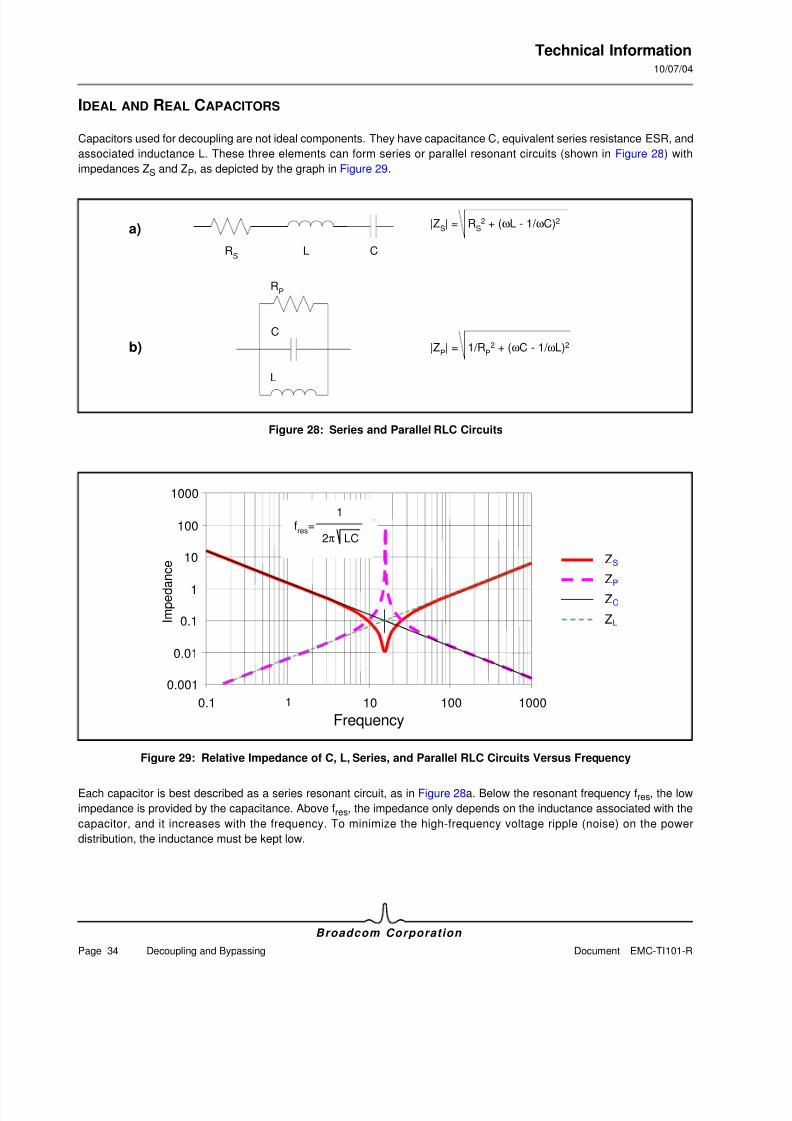
8/7/2019 Metodos_PCB
http://slidepdf.com/reader/full/metodospcb 40/54
Technical Information10/07/04
Broadcom Corporation
Page 34 Decoupling and Bypassing Document EMC-TI101-R
IDEAL AND REAL CAPACITORS
Capacitors used for decoupling are not ideal components. They have capacitance C, equivalent series resistance ESR, and
associated inductance L. These three elements can form series or parallel resonant circuits (shown in Figure 28) with
impedances ZS and ZP, as depicted by the graph in Figure 29.
Figure 28: Series and Parallel RLC Circuits
Figure 29: Relative Impedance of C, L, Series, and Parallel RLC Circuits Versus Frequency
Each capacitor is best described as a series resonant circuit, as in Figure 28a. Below the resonant frequency fres, the low
impedance is provided by the capacitance. Above fres, the impedance only depends on the inductance associated with the
capacitor, and it increases with the frequency. To minimize the high-frequency voltage ripple (noise) on the power
distribution, the inductance must be kept low.
a)
b)
RP
L
C
RS
L C
|ZP| = 1/R
P2 + (ωC - 1/ ωL)2
|ZS| = R
S2 + (ωL - 1/ ωC)2
0.001
0.01
0.1
1
10
100
1000
0.1 1 10 100 1000
Frequency
Impedan
ce
LCF res
π 2
1=
ZS
ZP ZC
ZL
fres
=1
2π LC
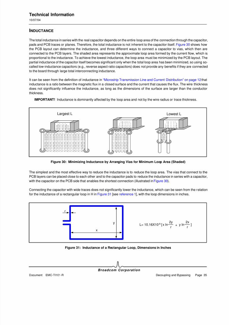
8/7/2019 Metodos_PCB
http://slidepdf.com/reader/full/metodospcb 41/54
Technical Information10/07/04
Broadcom Corporation
Document EMC-TI101-R Decoupling and Bypassing Page 35
INDUCTANCE
The total inductance in series with the real capacitor depends on the entire loop area of the connection through the capacitor,
pads and PCB traces or planes. Therefore, the total inductance is not inherent to the capacitor itself. Figure 30 shows how
the PCB layout can determine the inductance, and three different ways to connect a capacitor to vias, which then are
connected to the PCB layers. The shaded area represents the approximate loop area formed by the current flow, which is
proportional to the inductance. To achieve the lowest inductance, the loop area must be minimized by the PCB layout. The
partial inductance of the capacitor itself becomes significant only when the total loop area has been minimized, so using so-
called low-inductance capacitors (e.g., reverse aspect ratio capacitors) does not provide any benefits if they are connected
to the board through large total interconnecting inductance.
It can be seen from the definition of inductance in “Microstrip Transmission Line and Current Distribution” on page 12 that
inductance is a ratio between the magnetic flux in a closed surface and the current that causes the flux. The wire thickness
does not significantly influence the inductance, as long as the dimensions of the surface are larger than the conductor
thickness.
IMPORTANT! Inductance is dominantly affected by the loop area and not by the wire radius or trace thickness.
Figure 30: Minimizing Inductance by Arranging Vias for Minimum Loop Area (Shaded)
The simplest and the most effective way to reduce the inductance is to reduce the loop area. The vias that connect to the
PCB layers can be placed close to each other and to the capacitor pads to reduce the inductance in series with a capacitor,
with the capacitor on the PCB side that enables the shortest connection (illustrated in Figure 30).
Connecting the capacitor with wide traces does not significantly lower the inductance, which can be seen from the relation
for the inductance of a rectangular loop in H in Figure 31 [see reference 1], with the loop dimensions in inches.
Figure 31: Inductance of a Rectangular Loop, Dimensions in Inches
Largest L Lowest L
L= 10.16X10⁻⁹ x ln2y
r y ln2x
r+[ ]
x
y
r
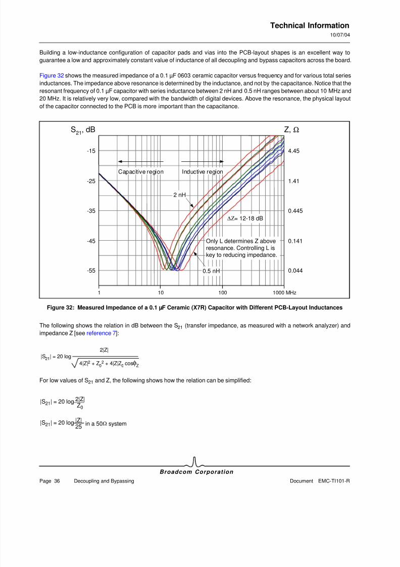
8/7/2019 Metodos_PCB
http://slidepdf.com/reader/full/metodospcb 42/54
Technical Information10/07/04
Broadcom Corporation
Page 36 Decoupling and Bypassing Document EMC-TI101-R
Building a low-inductance configuration of capacitor pads and vias into the PCB-layout shapes is an excellent way to
guarantee a low and approximately constant value of inductance of all decoupling and bypass capacitors across the board.
Figure 32 shows the measured impedance of a 0.1 µF 0603 ceramic capacitor versus frequency and for various total series
inductances. The impedance above resonance is determined by the inductance, and not by the capacitance. Notice that the
resonant frequency of 0.1 µF capacitor with series inductance between 2 nH and 0.5 nH ranges between about 10 MHz and
20 MHz. It is relatively very low, compared with the bandwidth of digital devices. Above the resonance, the physical layoutof the capacitor connected to the PCB is more important than the capacitance.
Figure 32: Measured Impedance of a 0.1 µF Ceramic (X7R) Capacitor with Different PCB-Layout Inductances
The following shows the relation in dB between the S21 (transfer impedance, as measured with a network analyzer) and
impedance Z [see reference 7]:
For low values of S21 and Z, the following shows how the relation can be simplified:
1 10 100 1000 MHz
-55
-45
-35
-25
-15
S21
, dB
0.044
0.141
0.445
1.41
4.45
Z, Ω
∆Ζ = 12-18 dB
2 nH
0.5 nH
Only L determines Z aboveresonance. Controlling L iskey to reducing impedance.
Capacitive region Inductive region
2|Z|
4|Z|2 + Z02 + 4|Z|Z0 cosφZ
|S21| = 20 log
|S21| = 20 log 2|Z|Z0
|S21| = 20 log |Z|25
in a 50Ω system
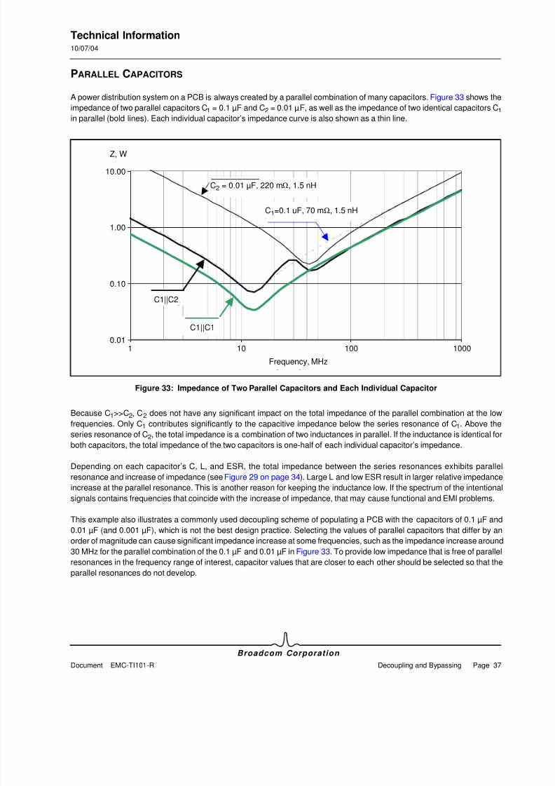
8/7/2019 Metodos_PCB
http://slidepdf.com/reader/full/metodospcb 43/54
Technical Information10/07/04
Broadcom Corporation
Document EMC-TI101-R Decoupling and Bypassing Page 37
PARALLEL CAPACITORS
A power distribution system on a PCB is always created by a parallel combination of many capacitors. Figure 33 shows the
impedance of two parallel capacitors C1 = 0.1 µF and C2 = 0.01 µF, as well as the impedance of two identical capacitors C1
in parallel (bold lines). Each individual capacitor’s impedance curve is also shown as a thin line.
Figure 33: Impedance of Two Parallel Capacitors and Each Individual Capacitor
Because C1>>C2, C2 does not have any significant impact on the total impedance of the parallel combination at the low
frequencies. Only C1 contributes significantly to the capacitive impedance below the series resonance of C1. Above the
series resonance of C2, the total impedance is a combination of two inductances in parallel. If the inductance is identical for
both capacitors, the total impedance of the two capacitors is one-half of each individual capacitor’s impedance.
Depending on each capacitor’s C, L, and ESR, the total impedance between the series resonances exhibits parallel
resonance and increase of impedance (see Figure 29 on page 34). Large L and low ESR result in larger relative impedance
increase at the parallel resonance. This is another reason for keeping the inductance low. If the spectrum of the intentional
signals contains frequencies that coincide with the increase of impedance, that may cause functional and EMI problems.
This example also illustrates a commonly used decoupling scheme of populating a PCB with the capacitors of 0.1 µF and
0.01 µF (and 0.001 µF), which is not the best design practice. Selecting the values of parallel capacitors that differ by an
order of magnitude can cause significant impedance increase at some frequencies, such as the impedance increase around30 MHz for the parallel combination of the 0.1 µF and 0.01 µF in Figure 33. To provide low impedance that is free of parallel
resonances in the frequency range of interest, capacitor values that are closer to each other should be selected so that the
parallel resonances do not develop.
10.00
1.00
0.10
0.01
Im
edance ?
1 100010010
Frequency, MHz
C 1 || C 1
C 1 || C 2
C 2 = 0.01 µF, 220 m? , 1.5 nH
C 1 = 0.1 µF, 70 m? , 1.5 nH
0.01
10.00
1.00
0.10
Z, W
Frequency, MHz
10001 10 100
C1= 0.1 µF, 220 mΩ, 1.5 nH
C2= 0.01 µF, 220 mΩ, 1.5 nH
C1||C2
C1||C1
C2 = 0.01 µF, 220 mΩ, 1.5 nH
C1=0.1 uF, 70 mΩ, 1.5 nH

8/7/2019 Metodos_PCB
http://slidepdf.com/reader/full/metodospcb 44/54
Technical Information10/07/04
Broadcom Corporation
Page 38 Decoupling and Bypassing Document EMC-TI101-R
It is also possible, and a good practice, to minimize the parallel resonance impedance by using a number of capacitors of
the same value, usually the largest capacitance for a given package size. Figure 33 on page 37 also shows a total
impedance of two capacitors with the same C, ESR, and L (C1||C1). The likelihood of developing the parallel resonances is
reduced and the total capacitance is larger than with mixed capacitor values, which results in lower total impedance at the
lower frequencies. This does not significantly influence the high-frequency impedance, which is determined by the
inductance. Again, the key to lowering impedance at high frequencies is lowering the inductance.
At the frequencies above several hundred MHz, the PCB planes significantly affect the total impedance of the PCB-level
power supply. While it is true that the capacitance increases with decrease of the plane spacing, the most important effect
is that the inductance between the planes decreases. The major benefit of spacing the Vcc and L0 planes close together is
the decrease of inductance between the planes. Lowering the inductance of the planes reduces the impedance of the PCB-
level power distribution system. The significant consequence for EMI is that the CM-mode voltages across the planes are
reduced when lowering inductance in the PCB-level power supply.
A simulation tool can be useful for design of decoupling and bypassing. The tool should be able to take into account the
transmission line properties of the power distribution system and proper RLC elements for the capacitors. It should be noted
that the discussion above illustrates the behavior of the capacitors and importance of minimizing the inductance when laying
them out on a PCB. The total impedance of the power distribution system on the typical PCBs is a much more complicated
combination of the discrete capacitors, impedance of the PCB planes, and impedance of all the other components that are
connected to the power distribution system.
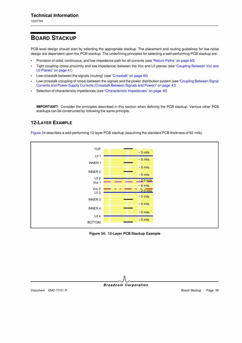
8/7/2019 Metodos_PCB
http://slidepdf.com/reader/full/metodospcb 45/54
Technical Information10/07/04
Broadcom Corporation
Document EMC-TI101-R Board Stackup Page 39
BOARD STACKUP
PCB-level design should start by selecting the appropriate stackup. The placement and routing guidelines for low-noise
design are dependent upon the PCB stackup. The underlining principles for selecting a well-performing PCB stackup are:
• Provision of solid, continuous, and low impedance path for all currents (see “Return Paths” on page 40)
• Tight coupling (close proximity and low impedance) between the Vcc and L0 planes (see “Coupling Between Vcc andL0 Planes” on page 41)
• Low crosstalk between the signals (routing) (see “Crosstalk” on page 40)
• Low crosstalk (coupling of noise) between the signals and the power distribution system (see “Coupling Between SignalCurrents and Power Supply Currents (Crosstalk Between Signals and Power)” on page 41)
• Selection of characteristic impedances (see “Characteristic Impedances” on page 40)
IMPORTANT! Consider the principles described in this section when defining the PCB stackup. Various other PCBstackups can be constructed by following the same principle.
12-LAYER EXAMPLE
Figure 34 describes a well-performing 12-layer PCB stackup (assuming the standard PCB thickness of 62 mils).
Figure 34: 12-Layer PCB Stackup Example
TOP
L0 1
L0 2
Vcc 1
Vcc 2
INNER 1
INNER 2
INNER 3
INNER 4
BOTTOM
L0 3
L0 4
~ 5 mils
~ 5 mils
~ 2-3 mils
~ 2-3 mils
~ 5 mils
~ 5 mils
~ 5 mils
~ 5 mils
~ 6 mils
~ 6 mils
~ 6 mils
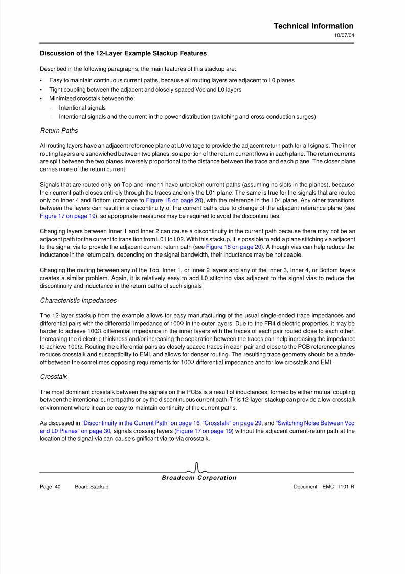
8/7/2019 Metodos_PCB
http://slidepdf.com/reader/full/metodospcb 46/54
Technical Information10/07/04
Broadcom Corporation
Page 40 Board Stackup Document EMC-TI101-R
Discussion of the 12-Layer Example Stackup Features
Described in the following paragraphs, the main features of this stackup are:
• Easy to maintain continuous current paths, because all routing layers are adjacent to L0 planes
• Tight coupling between the adjacent and closely spaced Vcc and L0 layers
• Minimized crosstalk between the:- Intentional signals
- Intentional signals and the current in the power distribution (switching and cross-conduction surges)
Return Paths
All routing layers have an adjacent reference plane at L0 voltage to provide the adjacent return path for all signals. The inner
routing layers are sandwiched between two planes, so a portion of the return current flows in each plane. The return currents
are split between the two planes inversely proportional to the distance between the trace and each plane. The closer plane
carries more of the return current.
Signals that are routed only on Top and Inner 1 have unbroken current paths (assuming no slots in the planes), because
their current path closes entirely through the traces and only the L01 plane. The same is true for the signals that are routed
only on Inner 4 and Bottom (compare to Figure 18 on page 20), with the reference in the L04 plane. Any other transitions
between the layers can result in a discontinuity of the current paths due to change of the adjacent reference plane (see
Figure 17 on page 19), so appropriate measures may be required to avoid the discontinuities.
Changing layers between Inner 1 and Inner 2 can cause a discontinuity in the current path because there may not be an
adjacent path for the current to transition from L01 to L02. With this stackup, it is possible to add a plane stitching via adjacent
to the signal via to provide the adjacent current return path (see Figure 18 on page 20). Although vias can help reduce the
inductance in the return path, depending on the signal bandwidth, their inductance may be noticeable.
Changing the routing between any of the Top, Inner 1, or Inner 2 layers and any of the Inner 3, Inner 4, or Bottom layers
creates a similar problem. Again, it is relatively easy to add L0 stitching vias adjacent to the signal vias to reduce the
discontinuity and inductance in the return paths of such signals.
Characteristic Impedances
The 12-layer stackup from the example allows for easy manufacturing of the usual single-ended trace impedances and
differential pairs with the differential impedance of 100Ω in the outer layers. Due to the FR4 dielectric properties, it may be
harder to achieve 100Ω differential impedance in the inner layers with the traces of each pair routed close to each other.
Increasing the dielectric thickness and/or increasing the separation between the traces can help increasing the impedance
to achieve 100Ω. Routing the differential pairs as closely spaced traces in each pair and close to the PCB reference planes
reduces crosstalk and susceptibility to EMI, and allows for denser routing. The resulting trace geometry should be a trade-
off between the sometimes opposing requirements for 100Ω differential impedance and for low crosstalk and EMI.
Crosstalk
The most dominant crosstalk between the signals on the PCBs is a result of inductances, formed by either mutual coupling
between the intentional current paths or by the discontinuous current path. This 12-layer stackup can provide a low-crosstalk
environment where it can be easy to maintain continuity of the current paths.
As discussed in “Discontinuity in the Current Path” on page 16, “Crosstalk” on page 29, and “Switching Noise Between Vcc
and L0 Planes” on page 30, signals crossing layers (Figure 17 on page 19) without the adjacent current-return path at the
location of the signal-via can cause significant via-to-via crosstalk.
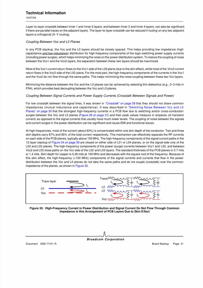
8/7/2019 Metodos_PCB
http://slidepdf.com/reader/full/metodospcb 47/54
Technical Information10/07/04
Broadcom Corporation
Document EMC-TI101-R Board Stackup Page 41
Layer-to-layer crosstalk between Inner 1 and Inner 2 layers, and between Inner 3 and Inner 4 layers, can also be significant
if there are parallel traces on the adjacent layers. The layer-to-layer crosstalk can be reduced if routing on any two adjacent
layers is orthogonal (X–Y routing).
Coupling Between Vcc and L0 Planes
In any PCB stackup, the Vcc and the L0 layers should be closely spaced. This helps providing low impedance (highcapacitance and low inductance) distribution for high-frequency components of the logic-switching power supply currents
(including power surges), which helps minimizing the noise on the power distribution system. To reduce the coupling of noise
between the Vcc1 and the Vcc2 layers, the separation between these two layers should be maximized.
Most of the Vcc1 current return flows on the Vcc1 side of the L02 plane (due to the skin effect), while most of the Vcc2 current
return flows in the Vcc2 side of the L03 plane. For the most part, the high-frequency components of the currents in the Vcc1
and the Vcc2 do not flow through the same paths. This helps minimizing the noise coupling between these two Vcc layers.
Minimizing the distance between the Vcc and the L0 planes can be achieved by selecting thin dielectrics (e.g., 2–3 mils in
FR4), which provides best decoupling between the Vcc and L0 planes.
Coupling Between Signal Currents and Power Supply Currents (Crosstalk Between Signals and Power)
For low crosstalk between the signal lines, it was shown in “Crosstalk” on page 29 that they should not share common
impedances (mutual inductance and capacitance). It was described in “Switching Noise Between Vcc and L0
Planes” on page 30 that the strongest high-frequency currents in a PCB flow due to switching and/or cross-conduction
surges between the Vcc and L0 planes (Figure 26 on page 31) and their peak values measure in amperes (of transient
current) as opposed to the signal currents that usually have much lower levels. The coupling of noise between the signals
and current surges in the power distribution can be significant and cause EMI and functional issues.
At high frequencies, most of the current (about 63%) is concentrated within one skin depth of the conductor. Two and three
skin depths carry 87% and 95% of the total current respectively. This mechanism can effectively separate the RF currents
on each side of the PCB planes, typically above 100 MHz. The high-frequency components of the signal current paths in the
12-layer stackup of Figure 34 on page 39 are closed on either side of L01 or L04 planes, or on the signal-side only of the
L02 and L03 planes. The high-frequency components of the power (surge) currents between Vcc1 and L02, and between
Vcc2 and L03 close paths on the Vcc side of the L02 and L03 layers. The standard thickness of the PCB planes is 0.7 mils
or 1.4 mils. Skin depth for copper is 0.26 mils at 100 MHz and decreases with the square root of the frequency. Because of
this skin effect, the high-frequency (>100 MHz) components of the signal currents and currents that flow in the power
distribution between the Vcc and L0 planes do not take the same paths and do not couple (crosstalk) over the common
impedance of the planes, as shown in Figure 35.
Figure 35: High-Frequency Current in Power Distribution and Signal Current Do Not Flow Through CommonImpedance in this Arrangement of PCB Layers Due to Skin Effect
IS
IP
IP
L0
Vcc
L0
TraceIS
IS
IP
L0
Vcc
Trace layer

8/7/2019 Metodos_PCB
http://slidepdf.com/reader/full/metodospcb 48/54
Technical Information10/07/04
Broadcom Corporation
Page 42 Board Stackup Document EMC-TI101-R
Another consideration is low-frequency noise coupling, such as between the switch-mode power supplies and signal traces.
The skin effect does not provide isolation by the PCB planes at low frequencies. Therefore, sensitive analog and single-
ended signals should not be routed under the PCB sections containing strong sources of low frequency noise.
Split Vcc Planes
The routing layers are not adjacent to the Vcc planes in the 12-layer stackup example (Figure 34 on page 39), thus the Vccplanes can be easily used for multiple voltages. The gaps in the Vcc layers cannot cause any discontinuity in the signal return
paths. The size of the power planes in this stackup should only be large as necessary to encompass the pins that connect
to it. Limiting the size of the Vcc planes reduces the edge-effects described in “EM Field Propagation at the Edges of the
Planes” on page 23.
REDUCING THE NUMBER OF PCB LAYER TRADE-OFFS
Cost is the driving factor in reducing the number of layers, which is often achieved by reducing the number of planes in the
PCB layers. All other things being equal, this inevitably results in decrease of performance. Understanding the possible
issues is a key to creating a PCB stackup that is still acceptable, even though it may not have the best possible performance.
Paying attention to the following can make a large difference in performance of such (less than ideal) PCB stackups:
• Current flow.
• Impedance between Vcc and L0.
• Coupling/crosstalk between the signals, and between the signal and the power distribution.
• Applying additional measures, such as:
- Providing additional intentional return paths
- Adding L0 fills
- Designing proper decoupling and bypassing
- Carefully examining the routing strategy
IMPORTANT! The following PCB stackups are not necessarily the best stackups from the performance point of view.
Because they are used to describe some performance issues that arise from compromising the performance criteria todecrease the cost, they intend to be illustrations of potential issues rather than recommendations.
Figure 36 on page 43 shows an example of a 10-layer stackup, which is a (cost-reduced) derivative of the 12-layer example,
where one L0 plane is removed and the other is replaced with a Vcc layer.
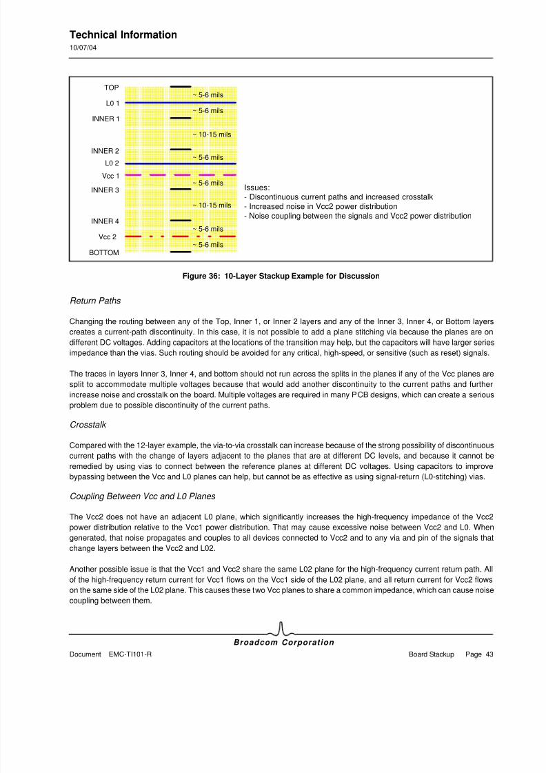
8/7/2019 Metodos_PCB
http://slidepdf.com/reader/full/metodospcb 49/54
Technical Information10/07/04
Broadcom Corporation
Document EMC-TI101-R Board Stackup Page 43
Figure 36: 10-Layer Stackup Example for Discussion
Return Paths
Changing the routing between any of the Top, Inner 1, or Inner 2 layers and any of the Inner 3, Inner 4, or Bottom layers
creates a current-path discontinuity. In this case, it is not possible to add a plane stitching via because the planes are on
different DC voltages. Adding capacitors at the locations of the transition may help, but the capacitors will have larger series
impedance than the vias. Such routing should be avoided for any critical, high-speed, or sensitive (such as reset) signals.
The traces in layers Inner 3, Inner 4, and bottom should not run across the splits in the planes if any of the Vcc planes are
split to accommodate multiple voltages because that would add another discontinuity to the current paths and further
increase noise and crosstalk on the board. Multiple voltages are required in many PCB designs, which can create a serious
problem due to possible discontinuity of the current paths.
Crosstalk
Compared with the 12-layer example, the via-to-via crosstalk can increase because of the strong possibility of discontinuous
current paths with the change of layers adjacent to the planes that are at different DC levels, and because it cannot be
remedied by using vias to connect between the reference planes at different DC voltages. Using capacitors to improve
bypassing between the Vcc and L0 planes can help, but cannot be as effective as using signal-return (L0-stitching) vias.
Coupling Between Vcc and L0 Planes
The Vcc2 does not have an adjacent L0 plane, which significantly increases the high-frequency impedance of the Vcc2
power distribution relative to the Vcc1 power distribution. That may cause excessive noise between Vcc2 and L0. When
generated, that noise propagates and couples to all devices connected to Vcc2 and to any via and pin of the signals that
change layers between the Vcc2 and L02.
Another possible issue is that the Vcc1 and Vcc2 share the same L02 plane for the high-frequency current return path. All
of the high-frequency return current for Vcc1 flows on the Vcc1 side of the L02 plane, and all return current for Vcc2 flows
on the same side of the L02 plane. This causes these two Vcc planes to share a common impedance, which can cause noise
coupling between them.
TOP
L0 1
L0 2
Vcc 1
Vcc 2
INNER 1
INNER 2
INNER 3
INNER 4
BOTTOM
~ 5-6 mils
~ 5-6 mils
~ 5-6 mils
~ 5-6 mils
~ 5-6 mils
~ 5-6 mils
~ 10-15 mils
~ 10-15 mils
Issues:- Discontinuous current paths and increased crosstalk
- Increased noise in Vcc2 power distribution
- Noise coupling between the signals and Vcc2 power distribution
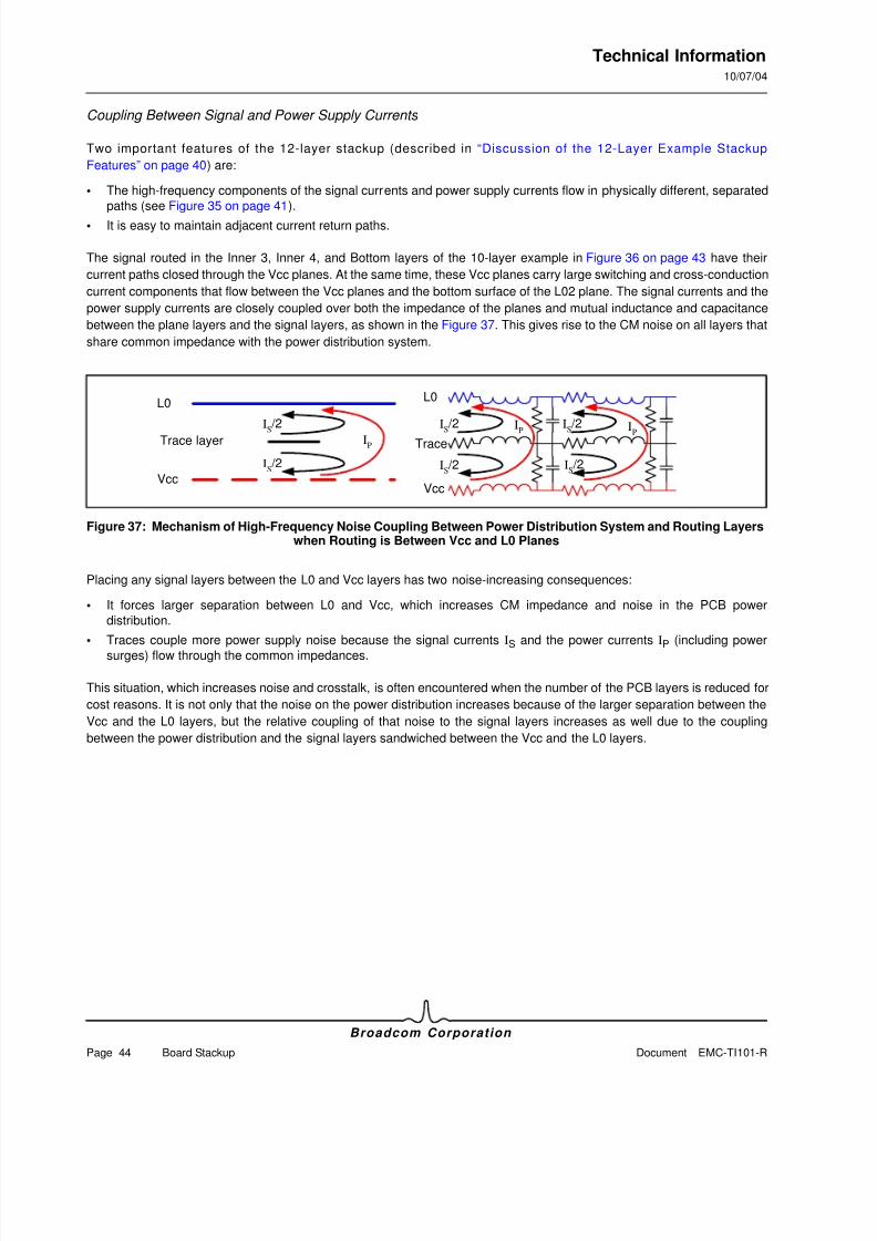
8/7/2019 Metodos_PCB
http://slidepdf.com/reader/full/metodospcb 50/54
Technical Information10/07/04
Broadcom Corporation
Page 44 Board Stackup Document EMC-TI101-R
Coupling Between Signal and Power Supply Currents
Two important features of the 12-layer stackup (described in “Discussion of the 12-Layer Example Stackup
Features” on page 40) are:
• The high-frequency components of the signal currents and power supply currents flow in physically different, separated
paths (see Figure 35 on page 41).
• It is easy to maintain adjacent current return paths.
The signal routed in the Inner 3, Inner 4, and Bottom layers of the 10-layer example in Figure 36 on page 43 have their
current paths closed through the Vcc planes. At the same time, these Vcc planes carry large switching and cross-conduction
current components that flow between the Vcc planes and the bottom surface of the L02 plane. The signal currents and the
power supply currents are closely coupled over both the impedance of the planes and mutual inductance and capacitance
between the plane layers and the signal layers, as shown in the Figure 37. This gives rise to the CM noise on all layers that
share common impedance with the power distribution system.
Figure 37: Mechanism of High-Frequency Noise Coupling Between Power Distribution System and Routing Layerswhen Routing is Between Vcc and L0 Planes
Placing any signal layers between the L0 and Vcc layers has two noise-increasing consequences:
• It forces larger separation between L0 and Vcc, which increases CM impedance and noise in the PCB power
distribution.
• Traces couple more power supply noise because the signal currents IS and the power currents IP (including powersurges) flow through the common impedances.
This situation, which increases noise and crosstalk, is often encountered when the number of the PCB layers is reduced for
cost reasons. It is not only that the noise on the power distribution increases because of the larger separation between the
Vcc and the L0 layers, but the relative coupling of that noise to the signal layers increases as well due to the coupling
between the power distribution and the signal layers sandwiched between the Vcc and the L0 layers.
L0
Vcc
Trace layer
IS/2
IS/2IP
Vcc
L0
TraceIS/2
IS/2
IS/2
IS/2
IPIP
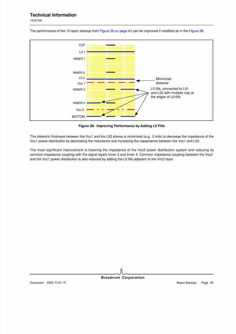
8/7/2019 Metodos_PCB
http://slidepdf.com/reader/full/metodospcb 51/54
Technical Information10/07/04
Broadcom Corporation
Document EMC-TI101-R Board Stackup Page 45
The performance of the 10-layer stackup from Figure 36 on page 43 can be improved if modified as in the Figure 38.
Figure 38: Improving Performance by Adding L0 Fills
The dielectric thickness between the Vcc1 and the L02 planes is minimized (e.g., 2 mils) to decrease the impedance of the
Vcc1 power distribution by decreasing the inductance and increasing the capacitance between the Vcc1 and L02.
The most significant improvement is lowering the impedance of the Vcc2 power distribution system and reducing its
common-impedance coupling with the signal layers Inner 3 and Inner 4. Common impedance coupling between the Vcc2
and the Vcc1 power distribution is also reduced by adding the L0 fills adjacent to the Vcc2 layer.
L0 fills, connected to L01
and L02 with multiple vias atthe edges of L0-fills
Minimized
distance
TOP
L0 1
L0 2
Vcc 1
Vcc 2
INNER 1
INNER 2
INNER 3
INNER 4
BOTTOM
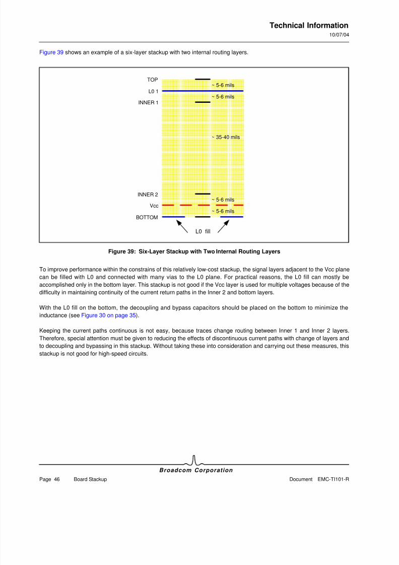
8/7/2019 Metodos_PCB
http://slidepdf.com/reader/full/metodospcb 52/54
Technical Information10/07/04
Broadcom Corporation
Page 46 Board Stackup Document EMC-TI101-R
Figure 39 shows an example of a six-layer stackup with two internal routing layers.
Figure 39: Six-Layer Stackup with Two Internal Routing Layers
To improve performance within the constrains of this relatively low-cost stackup, the signal layers adjacent to the Vcc plane
can be filled with L0 and connected with many vias to the L0 plane. For practical reasons, the L0 fill can mostly be
accomplished only in the bottom layer. This stackup is not good if the Vcc layer is used for multiple voltages because of the
difficulty in maintaining continuity of the current return paths in the Inner 2 and bottom layers.
With the L0 fill on the bottom, the decoupling and bypass capacitors should be placed on the bottom to minimize the
inductance (see Figure 30 on page 35).
Keeping the current paths continuous is not easy, because traces change routing between Inner 1 and Inner 2 layers.
Therefore, special attention must be given to reducing the effects of discontinuous current paths with change of layers and
to decoupling and bypassing in this stackup. Without taking these into consideration and carrying out these measures, this
stackup is not good for high-speed circuits.
~ 35-40 mils
~ 5-6 mils
~ 5-6 mils
~ 5-6 mils
~ 5-6 mils
TOP
L0 1
INNER 1
Vcc
INNER 2
BOTTOM
L0 fill
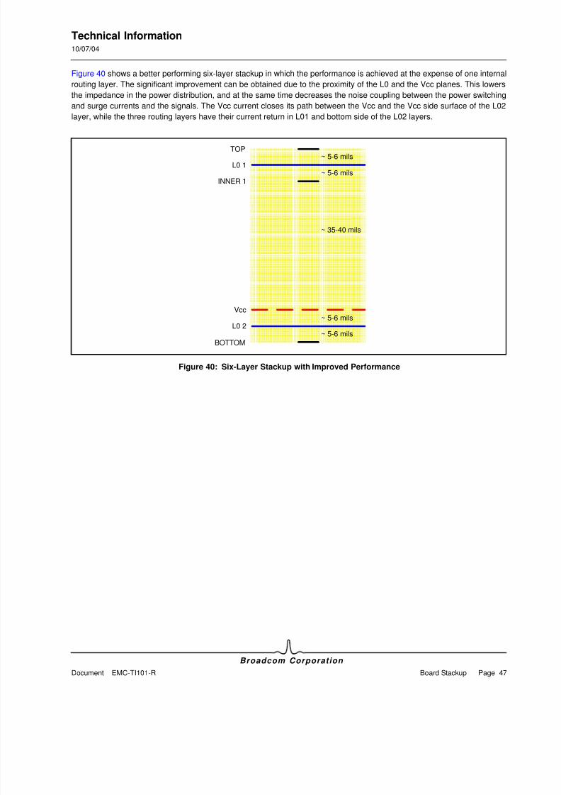
8/7/2019 Metodos_PCB
http://slidepdf.com/reader/full/metodospcb 53/54
Technical Information10/07/04
Broadcom Corporation
Document EMC-TI101-R Board Stackup Page 47
Figure 40 shows a better performing six-layer stackup in which the performance is achieved at the expense of one internal
routing layer. The significant improvement can be obtained due to the proximity of the L0 and the Vcc planes. This lowers
the impedance in the power distribution, and at the same time decreases the noise coupling between the power switching
and surge currents and the signals. The Vcc current closes its path between the Vcc and the Vcc side surface of the L02
layer, while the three routing layers have their current return in L01 and bottom side of the L02 layers.
Figure 40: Six-Layer Stackup with Improved Performance
~ 35-40 mils
~ 5-6 mils
~ 5-6 mils
~ 5-6 mils
~ 5-6 mils
TOP
L0 1
INNER 1
Vcc
BOTTOM
L0 2

8/7/2019 Metodos_PCB
http://slidepdf.com/reader/full/metodospcb 54/54
Broadcom Corporation
16215 Alton ParkwayP.O. Box 57013
Irvine, CA 92619-7013Phone: 949-450-8700
Fax: 949-450-8710
Broadcom® Corporation reserves the right to make changes without further notice to any products or data herein to improve reliability, function, or design.Information furnished by Broadcom Corporation is believed to be accurate and reliable. However, Broadcom Corporation
d t li bilit i i t f th li ti f thi i f ti th li ti f d t
Technical Information10/07/04
REFERENCES AND LITERATURE
REFERENCES
[1] Howard W. Johnson, Martin Graham: High Speed Digital Design, PTR Prentice-Hall, Inc.
[2] Henry W. Ott: Noise Reduction Techniques in Electronic Systems, John Wiley & Sons, Inc.
[3] W.M. King: EMCT—Electromagnetic Compatibility Tutorial, produced by Elliott Laboratories, Sunnyvale, CA and IEEE-
Standards Information Network
[4] D. M. Hockanson, J. L. Drewniak, T. H. Hubing, T. P. Van Doren, F. Sha, C.-W. Lam, and L. Rubin: Quantifying EMI
Resulting from Finite-Impedance Reference Planes, IEEE Transaction on EMC, Vol. 39, Nov. 1997
[5] Marco Leone: Design Expressions for the Trace-to-Edge Common-Mode Inductance of a Printed Circuit Board, IEEE
Trans. on EMC, vol.43, no. 4, November 2001
[6] J. Lockwood, E. Pavlu, US Patent 5,898,576 "Printed Circuit Board Including a Terminated Power Plane and Method of
Manufacturing the Same", April 1999
[7] Jeffrey Cain, Steve Makl: Capacitor Selection and EMI Filtering, AVX Corporation Technical Information
LITERATURE
• Clayton R. Paul: Introduction to Electromagnetic Compatibility, John Wiley & Sons, Inc.
• Stephen H. Hall, Garrett W. Hall, James A. McCall: High-Speed Digital System Design, John Wiley & Sons, Inc.


