Embed Size (px)
Citation preview
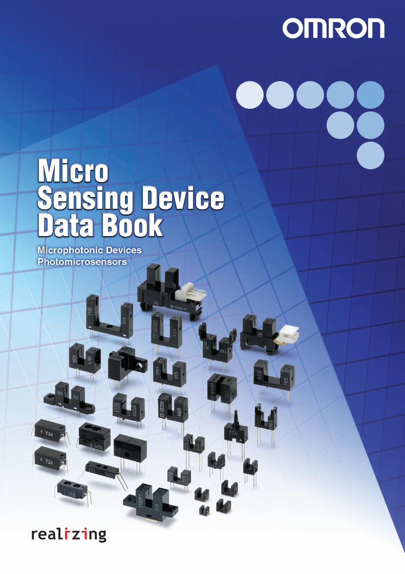

CONTENTS
1
Selection Guide . . . . . . . . . . . . . . . . . . . . . . . . . . . . . . . . . . . . 2Microphotonic Devices
Manuscript Paper Sensors . . . . . . . . . . . . . . . . . . . . . . . . . . . . . . . . . 6Photomicrosensors
Technical Information . . . . . . . . . . . . . . . . . . . . . . . . . . . . . . . . . . . . 12Precautions . . . . . . . . . . . . . . . . . . . . . . . . . . . . . . . . . . . . . . . . . . . . . 25Application Examples . . . . . . . . . . . . . . . . . . . . . . . . . . . . . . . . . . . . 28Transmissive Photomicrosensors . . . . . . . . . . . . . . . . . . . . . . . . . . . . 30Reflective Photomicrosensors . . . . . . . . . . . . . . . . . . . . . . . . . . . . . . 150
General InformationReliability . . . . . . . . . . . . . . . . . . . . . . . . . . . . . . . . . . . . . . . . . . . . . . 176Security Trade Control . . . . . . . . . . . . . . . . . . . . . . . . . . . . . . . . . . . . 185

Selection GuideSensing method
Sensing distance Model Output configuration Features Page
Transmissive 1.0 mm EE-SX1107 Phototransistor Ultra-compact, surface mounting 62
2.0 mm EE-SX1018 Phototransistor Compact, general purpose 30
EE-SX1049 Phototransistor Compact, general purpose 40
EE-SX1103 Phototransistor Ultra-compact, general purpose 56
EE-SX1105 Phototransistor Ultra-compact, general purpose 58
EE-SX1108 Phototransistor Ultra-compact, surface mounting 66
EE-SX1131 Phototransistor Ultra-compact, surface mounting, dual-channel output
78
EE-SX4134 Photo-IC Ultra-compact, surface mounting 136
EE-SX493 Photo-IC High resolution 130
2.8 mm EE-SX1055 Phototransistor Compact, excellent cost performance 42
3.0 mm EE-SX1046 Phototransistor With a horizontal aperture 38
EE-SX1106 Phototransistor Ultra-compact, general purpose 60
EE-SX1109 Phototransistor Ultra-compact, surface mounting 70
EE-SX129 Phototransistor High resolution 88
EE-SX198 Phototransistor General purpose 94
EE-SX199 Phototransistor With a positioning boss 96
EE-SX298 Photo-Darlington transistor General purpose 116
EE-SX398/498 Photo-IC General purpose 132
3.4 mm EE-SX1071 Phototransistor General purpose 48
EE-SX1088 Phototransistor Screw mounting 52
EE-SX1096 Phototransistor With a horizontal aperture 54
EE-SX138 Phototransistor Screw mounting 90
EE-SX153 Phototransistor Screw mounting 92
EE-SH3 series Phototransistor Screw mounting 108
EE-SJ3 series Phototransistor Screw mounting 110
EE-SV3 series Phototransistor Screw mounting 114
EE-SX301/401 Photo-IC General purpose 118
EE-SX3088/4088 Photo-IC Screw mounting 124
3.5 mm EE-SX384/484 Photo-IC General purpose 128
3.6 mm EE-SX1057 Phototransistor Dust-proof construction, general purpose 44
EE-SG3(-B) Phototransistor Dust-proof construction 106
4.2 mm EE-SX1128 Phototransistor With a horizontal aperture 76
5.0 mm EE-SX1041 Phototransistor General purpose 34
EE-SX1042 Phototransistor High profile 36
EE-SX1081 Phototransistor General purpose 50
EE-SX1115 Phototransistor High profile with positioning pins 74
EE-SX1137 Phototransistor General purpose 82
EE-SX1235A-P2 Phototransistor Snap-in mounting 86
5.0 mm EE-SJ5-B Phototransistor General purpose 112
3.6 mm EE-SX3148-P1 Photo-IC Screw mounting 126
2 Selection Guide

Transmissive 5.0 mm EE-SX3081/4081 Photo-IC General purpose 122
EE-SX3239-P2 Photo-IC Snap-in mounting 142
EE-SX3009-P1/4009-P1
Photo-IC Screw mounting 134
EE-SX4235A-P2 Photo-IC Snap-in mounting 140
EE-SX460-P1 Photo-IC Snap-in mounting 144
5.2 mm EE-SX1035 Phototransistor Compact, wide 32
8.0 mm EE-SX1070 Phototransistor General purpose 46
EE-SX3070/4070 Photo-IC General purpose 120
15.0 mm EE-SX461-P11 Photo-IC Easy to mount 146
14 mm EE-SX1140 Phototransistor Wide, high profile 84
Actuator mount-ing
--- EE-SA102 Phototransistor General purpose 98
EE-SA104 Phototransistor Compact 100
EE-SA407-P2 Photo-IC Easy to mount 148
Actuator --- EE-SA105 Phototransistor General purpose 102
EE-SA113 Phototransistor General purpose 104
Reflective 1.0 mm EE-SY193 Phototransistor Ultra-compact, surface mounting 162
3.5 mm EE-SY171 Phototransistor Thin 160
4.0 mm EE-SY169 Phototransistor High resolution (red LED) 154
EE-SY169A Phototransistor High resolution (infrared LED) 156
EE-SY169B Phototransistor High resolution (red LED) 158
4.4 mm EE-SY113 Phototransistor Dust-proof 152
EE-SY313/413 Photo-IC Dust-proof 172
5.0 mm EE-SY110 Phototransistor General purpose 150
EE-SB5(-B) Phototransistor Screw mounting 166
EE-SF5(-B) Phototransistor Dust-proof 168
EE-SY310/410 Photo-IC General purpose 170
Sensing method
Sensing distance Model Output configuration Features Page
Selection Guide 3

4 Selection Guide
5
Microphotonic DevicesManuscript Paper Sensors
EY3A-1051 . . . . . . . . . . . . . . . . . . . . . . . . . . . . . . . . . . . . . . . . . . . . . . . 6EY3A-1081 . . . . . . . . . . . . . . . . . . . . . . . . . . . . . . . . . . . . . . . . . . . . . . . 8
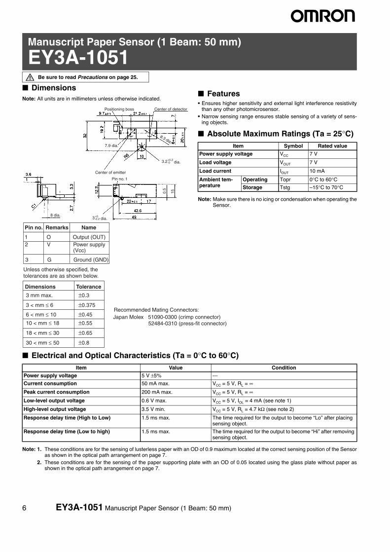
Manuscript Paper Sensor (1 Beam: 50 mm)
EY3A-1051Be sure to read Precautions on page 25.
■ DimensionsNote: All units are in millimeters unless otherwise indicated.
■ Features• Ensures higher sensitivity and external light interference resistivity
than any other photomicrosensor.• Narrow sensing range ensures stable sensing of a variety of sens-
ing objects.
■ Absolute Maximum Ratings (Ta = 25°C)
Note: Make sure there is no icing or condensation when operating theSensor.
■ Electrical and Optical Characteristics (Ta = 0°C to 60°C)
Note: 1. These conditions are for the sensing of lusterless paper with an OD of 0.9 maximum located at the correct sensing position of the Sensoras shown in the optical path arrangement on page 7.
2. These conditions are for the sensing of the paper supporting plate with an OD of 0.05 located using the glass plate without paper asshown in the optical path arrangement on page 7.
Positioning boss Center of detector
Center of emitter
Pin no. 1
8.3 dia.
3.2+0.2-0 dia.
7.9 dia.
3+0-0.2 dia.
8 dia.
0.5
15
Item Symbol Rated value
Power supply voltage VCC 7 V
Load voltage VOUT 7 V
Load current IOUT 10 mA
Ambient tem-perature
Operating Topr 0°C to 60°CStorage Tstg –15°C to 70°C
Item Value Condition
Power supply voltage 5 V ±5% ---
Current consumption 50 mA max. VCC = 5 V, RL = ∞
Peak current consumption 200 mA max. VCC = 5 V, RL = ∞
Low-level output voltage 0.6 V max. VCC = 5 V, IOL = 4 mA (see note 1)
High-level output voltage 3.5 V min. VCC = 5 V, RL = 4.7 kΩ (see note 2)
Response delay time (High to Low) 1.5 ms max. The time required for the output to become “Lo” after placing sensing object.
Response delay time (Low to high) 1.5 ms max. The time required for the output to become “Hi” after removing sensing object.
Dimensions Tolerance
3 mm max. ±0.3
3 < mm ≤ 6 ±0.375
6 < mm ≤ 10 ±0.45
10 < mm ≤ 18 ±0.55
18 < mm ≤ 30 ±0.65
30 < mm ≤ 50 ±0.8
Pin no. Remarks Name
3 G Ground (GND)
1 O Output (OUT)2 V Power supply
(Vcc)
Unless otherwise specified, the tolerances are as shown below.
Japan Molex 51090-0300 (crimp connector) 52484-0310 (press-fit connector)
Recommended Mating Connectors:
6 EY3A-1051 Manuscript Paper Sensor (1 Beam: 50 mm)

■ Characteristics (Paper Table Glass: t = 6 mm max., Transparency Rate: 90% min.)(Ta =0°C to 60°C)
Note: 1. The data shown are initial data.2. Optical darkness (OD) is defined by the following formula:
PIN (mW): Light power incident upon the document
POUT (mW): Reflected light power from the document
■ Optical Path Arrangement
■ Engineering Data
Item Characteristic value
Sensing density Lusterless paper with an OD of 0.9 max. (sensing distance: 50 mm) (see note)
Non-sensing distance 85 mm (from the top of the sensor), OD: 0.05
Paper sensing distance 50 mm (from the top of the sensor)
Ambient illumination Sunlight: 3,000 lx max., fluorescent light: 2,000 lx max.
OD = − log10
POUT
PIN
2. The non-sensing distance of the EY3A-1051 is determined using a paper with an OD of 0.05.
85 (see note 2)
Paper supporting plate
10 dia. (see note 1)
50 (standard value)
Glass
8.9
Note: 1. The part with oblique lines indicates the paper sensing area of the EY3A-1051, which is practically determined by the diameter of the beam and its tolerance.
Distance Characteristics (Typical)
Distance (mm)
OD
(va
lue)
4.75 V 5.0 V 5.25 V
EY3A-1051 Manuscript Paper Sensor (1 Beam: 50 mm) 7

Manuscript Paper Sensor (1 Beam: 80 mm)
EY3A-1081Be sure to read Precautions on page 25.
■ DimensionsNote: All units are in millimeters unless otherwise indicated.
■ Features• Ensures higher sensitivity and external light interference resistivity
than any other photomicrosensor.• Narrow sensing range ensures stable sensing of a variety of sens-
ing objects.
■ Absolute Maximum Ratings (Ta = 25°C)
Note: Make sure there is no icing or condensation when operating theSensor.
■ Electrical and Optical Characteristics (Ta = 0°C to 60°C)
Note: 1. These conditions are for the sensing of lusterless paper with an OD of 0.7 maximum located at the correct sensing position of the Sensoras shown in the optical path arrangement on page 9.
2. These conditions are for the sensing of the paper supporting plate with an OD of 0.05 located using the glass plate without paper asshown in the optical path arrangement on page 9.
3 0-0.2 dia.
Positioning boss Center of detector
Center of emitter
Pin no.1
3.2 +0.20 dia.
7.9 dia. 8.3 dia. Item Symbol Rated value
Power supply voltage VCC 7 V
Load voltage VOUT 7 V
Load current IOUT 10 mA
Ambient tem-perature
Operating Topr 0°C to 60°CStorage Tstg –15°C to 70°C
Item Value Condition
Power supply voltage 5 V ±5% ---
Current consumption 50 mA max. VCC = 5 V, RL = ∞
Peak current consumption 200 mA max. VCC = 5 V, RL = ∞
Low-level output voltage 0.6 V max. VCC = 5 V, IOL = 4 mA (see note 1)
High-level output voltage 3.5 V min. VCC = 5 V, RL = 4.7 kΩ (see note 2)
Response delay time (High to Low) 1.5 ms max. The time required for the output to become “Lo” after placing sensing object.
Response delay time (Low to high) 1.5 ms max. The time required for the output to become “Hi” after removing sensing object.
Dimensions Tolerance
3 mm max. ±0.3
3 < mm ≤ 6 ±0.375
6 < mm ≤ 10 ±0.45
10 < mm ≤ 18 ±0.55
18 < mm ≤ 30 ±0.65
30 < mm ≤ 50 ±0.8
50 < mm ≤ 80 ±0.95
Pin no. Remarks Name
1 O Output (OUT)
2 V Power supply (Vcc)
3 G Ground (GND)
Unless otherwise specified, the tolerances are as shown below.
Japan Molex 51090-0300 (crimp connector) 52484-0310 (press-fit connector)
Recommended Mating Connectors:
8 EY3A-1081 Manuscript Paper Sensor (1 Beam: 80 mm)

■ Characteristics (Paper Table Glass: t = 6 mm max., Transparency Rate: 90% min.)(Ta =0°C to 60°C)
Note: 1. The data shown are initial data.2. Optical darkness (OD) is defined by the following formula:
PIN (mW):Light power incident upon the document
POUT (mW):Reflected light power from the document
■ Optical Path Arrangement
Note: 1. The part with oblique lines indicates the paper sensing area of the EY3A-1081, which is practically determined by the diameter of thebeam and its tolerance.
2. The non-sensing distance of the EY3A-1081 is determined using a paper with an OD of 0.05.
■ Engineering Data
Item Characteristic value
Sensing density Lusterless paper with an OD of 0.7 max. (sensing distance: 80 mm) (see note)
Non-sensing distance 120 mm (from the top of the sensor), OD: 0.05
Paper sensing distance 80 mm (from the top of the sensor)
Ambient illumination Sunlight: 3,000 lx max., fluorescent light: 2,000 lx max.
OD = − log10
POUT
PIN
10 dia. (see note 1)
Paper supporting plate Glass
120 (see note 2)
80 (Standard value)
4.75 V 5.0 V 5.25 V
Distance Characteristics (Typical)
Distance (mm)
OD
(va
lue)
EY3A-1081 Manuscript Paper Sensor (1 Beam: 80 mm) 9

10 EY3A-1081 Manuscript Paper Sensor (1 Beam: 80 mm)

11
PhotomicrosensorsTransmissive Sensors
Technical Information . . . . . . . . . . . . . . 12Precautions . . . . . . . . . . . . . . . . . . . . . 25Application Examples . . . . . . . . . . . . . . 28EE-SX1018. . . . . . . . . . . . . . . . . . . . . . 30EE-SX1035. . . . . . . . . . . . . . . . . . . . . . 32EE-SX1041. . . . . . . . . . . . . . . . . . . . . . 34EE-SX1042. . . . . . . . . . . . . . . . . . . . . . 36EE-SX1046. . . . . . . . . . . . . . . . . . . . . . 38EE-SX1049. . . . . . . . . . . . . . . . . . . . . . 40EE-SX1055. . . . . . . . . . . . . . . . . . . . . . 42EE-SX1057. . . . . . . . . . . . . . . . . . . . . . 44EE-SX1070. . . . . . . . . . . . . . . . . . . . . . 46EE-SX1071. . . . . . . . . . . . . . . . . . . . . . 48EE-SX1081. . . . . . . . . . . . . . . . . . . . . . 50EE-SX1088. . . . . . . . . . . . . . . . . . . . . . 52EE-SX1096. . . . . . . . . . . . . . . . . . . . . . 54EE-SX1103. . . . . . . . . . . . . . . . . . . . . . 56EE-SX1105. . . . . . . . . . . . . . . . . . . . . . 58EE-SX1106. . . . . . . . . . . . . . . . . . . . . . 60EE-SX1107. . . . . . . . . . . . . . . . . . . . . . 62EE-SX1108. . . . . . . . . . . . . . . . . . . . . . 66EE-SX1109. . . . . . . . . . . . . . . . . . . . . . 70EE-SX1115. . . . . . . . . . . . . . . . . . . . . . 74EE-SX1128. . . . . . . . . . . . . . . . . . . . . . 76EE-SX1131. . . . . . . . . . . . . . . . . . . . . . 78EE-SX1137. . . . . . . . . . . . . . . . . . . . . . 82EE-SX1140. . . . . . . . . . . . . . . . . . . . . . 84EE-SX1235A-P2. . . . . . . . . . . . . . . . . . 86EE-SX129. . . . . . . . . . . . . . . . . . . . . . . 88
EE-SX138 . . . . . . . . . . . . . . . . . . . . . . 90EE-SX153 . . . . . . . . . . . . . . . . . . . . . . 92EE-SX198 . . . . . . . . . . . . . . . . . . . . . . 94EE-SX199 . . . . . . . . . . . . . . . . . . . . . . 96EE-SA102 . . . . . . . . . . . . . . . . . . . . . . 98EE-SA104 . . . . . . . . . . . . . . . . . . . . . . 100EE-SA105 . . . . . . . . . . . . . . . . . . . . . . 102EE-SA113 . . . . . . . . . . . . . . . . . . . . . . 104EE-SG3/EE-SG3-B . . . . . . . . . . . . . . . 106EE-SH3 Series. . . . . . . . . . . . . . . . . . . 108EE-SJ3 Series . . . . . . . . . . . . . . . . . . . 110EE-SJ5-B . . . . . . . . . . . . . . . . . . . . . . . 112EE-SV3 Series . . . . . . . . . . . . . . . . . . . 114EE-SX298 . . . . . . . . . . . . . . . . . . . . . . 116EE-SX301/-SX401 . . . . . . . . . . . . . . . . 118EE-SX3070/-SX4070 . . . . . . . . . . . . . . 120EE-SX3081/-SX4081 . . . . . . . . . . . . . . 122EE-SX3088/-SX4088 . . . . . . . . . . . . . . 124EE-SX3148-P1. . . . . . . . . . . . . . . . . . . 126EE-SX384/-SX484 . . . . . . . . . . . . . . . . 128EE-SX493 . . . . . . . . . . . . . . . . . . . . . . 130EE-SX398/498 . . . . . . . . . . . . . . . . . . . 132EE-SX3009-P1/-SX4009-P1 . . . . . . . . 134EE-SX4134 . . . . . . . . . . . . . . . . . . . . . 136EE-SX4235A-P2 . . . . . . . . . . . . . . . . . 140EE-SX3239-P2. . . . . . . . . . . . . . . . . . . 142EE-SX460-P1. . . . . . . . . . . . . . . . . . . . 144EE-SX461-P11. . . . . . . . . . . . . . . . . . . 146EE-SA407-P2. . . . . . . . . . . . . . . . . . . . 148
Reflective SensorsEE-SY110. . . . . . . . . . . . . . . . . . . . . . . 150EE-SY113. . . . . . . . . . . . . . . . . . . . . . . 152EE-SY169. . . . . . . . . . . . . . . . . . . . . . . 154EE-SY169A . . . . . . . . . . . . . . . . . . . . . 156EE-SY169B . . . . . . . . . . . . . . . . . . . . . 158EE-SY171. . . . . . . . . . . . . . . . . . . . . . . 160EE-SY193. . . . . . . . . . . . . . . . . . . . . . . 162EE-SB5(-B). . . . . . . . . . . . . . . . . . . . . . 166EE-SF5(-B). . . . . . . . . . . . . . . . . . . . . . 168EE-SY310/-SY410 . . . . . . . . . . . . . . . . 170EE-SY313/-SY413 . . . . . . . . . . . . . . . . 172

Technical Information
Features of PhotomicrosensorsThe Photomicrosensor is a compact optical sensor that senses objects or object positions with an optical beam. The transmissive Photomicrosen-sor and reflective Photomicrosensor are typical Photomicrosensors.The transmissive Photomicrosensor incorporates an emitter and a transmissive that face each other as shown in Figure 1. When an object is lo-cated in the sensing position between the emitter and the detector, the object intercepts the optical beam of the emitter, thus reducing the amountof optical energy reaching the detector.The reflective Photomicrosensor incorporates an emitter and a detector as shown in Figure 2. When an object is located in the sensing area of thereflective Photomicrosensor, the object reflects the optical beam of the emitter, thus changing the amount of optical energy reaching the detector.“Photomicrosensor” is an OMRON product name. Generally, the Photomicrosensor is called a photointerrupter.
Datasheet
■ Absolute Maximum Ratings and Electrical and Optical Characteristics
The datasheets of Photomicrosensors include the absolute maximum ratings and electrical and optical characteristics of the Photomicrosensors as well as the datasheets of transistors and ICs. It is necessary to understand the difference between the absolute maximum ratings and electrical and optical characteristics of various Photomicrosensors.
■ Absolute Maximum RatingsThe absolute maximum ratings of Photomicrosensors and other products with semiconductors specify the permissible operating voltage, current, temperature, and power limits of these products. The products must be operated absolutely within these limits.Therefore, when using any Photomicrosensor, do not ignore the absolute maximum ratings of the Photomicrosensor, or the Photomicrosensor will not operate precisely. Furthermore, the Photomicrosensor may be deteriorate or become damaged, in which case OMRON will not be responsible.Practically, Photomicrosensors should be used so that there will be some margin between their absolute maximum ratings and actual operating conditions.
■ Electrical and Optical CharacteristicsThe electrical and optical characteristics of Photomicrosensors indicate the performance of Photomicrosensors under certain conditions. Most items of the electrical and optical characteristics are indicated by maximum or minimum values. OMRON usually sells Photomicrosensors with standard electrical and optical characteristics. The electrical and optical characteristics of Photomicrosensors sold to customers may be changed upon request. All electrical and optical characteristic items of Photomicrosensors indicated by maximum or minimum values are checked and those of the Photomicrosensors indicated by typical values are regularly checked before shipping so that OMRON can guarantee the performance of the Photomicrosensors.In short, the absolute maximum ratings indicate the permissible operating limits of the Photomicrosensors and the electrical and optical characteristics indicate the maximum performance of the Photomicrosensors.
Figure 1. Transmissive Photomicrosensor Figure 2. Reflective Photomicrosensor
LED Phototransistor LED Phototransistor
12 Technical Information

TerminologyThe terms used in the datasheet of each Photomicrosensor with a phototransistor output circuit or a photo IC output circuit are explained below.
■ Phototransistor Output Photomicrosensor
■ Phototransistor/Photo IC Output Photomicrosensor
Symbol Item Definition
IFP Pulse forward current The maximum pulse current that is allowed to flow continuously from the anode to cathode of an LED under a specified temperature, a repetition period, and a pulse width condition.
IC Collector current The current that flows to the collector junction of a phototransistor.
PC Collector dissipation The maximum power that is consumed by the collector junction of a phototransistor.
ID Dark current The current leakage of the phototransistor when a specified bias voltage is imposed on the phototrans-istor so that the polarity of the collector is positive and that of the emitter is negative on condition that the illumination of the Photomicrosensor is 0 lx.
IL Light current The collector current of a phototransistor under a specified input current condition and at a specified bias voltage.
VCE (sat) Collector-emitter saturated voltage
The ON-state voltage between the collector and emitter of a phototransistor under a specified bias cur-rent condition.
ILEAK Leakage current The collector current of a phototransistor under a specified input current condition and at a specified bias voltage when the phototransistor is not exposed to light.
tr Rising time The time required for the leading edge of an output waveform of a phototransistor to rise from 10% to 90% of its final value when a specified input current and bias condition is given to the phototransistor.
tf Falling time The time required for the trailing edge of an output waveform of a phototransistor to decrease from 90% to 10% of its final value when a specified input current and bias condition is given to the phototransistor.
VCEO Collector-emitter voltage The maximum positive voltage that can be applied to the collector of a phototransistor with the emitter at reference potential.
VECO Emitter-collector voltage The maximum positive voltage that can be applied to the emitter of a phototransistor with the collector at reference potential.
Symbol Item Definition
IF Forward current The maximum DC voltage that is allowed to flow continuously from the anode of the LED to the cathode of the LED under a specified temperature condition.
VR Reverse voltage The maximum negative voltage that can be applied to the anode of the LED with the cathode at refer-ence potential.
VCC Supply voltage The maximum positive voltage that can be applied to the voltage terminals of the photo IC with the ground terminal at reference potential.
VOUT Output voltage The maximum positive voltage that can be applied to the output terminal with the ground terminal of the photo IC at reference potential.
IOUT Output current The maximum current that is allowed to flow in the collector junction of the output transistor of the photo IC.
POUT Output permissible dissi-pation
The maximum power that is consumed by the collector junction of the output transistor of the photo IC.
VF Forward voltage The voltage drop across the LED in the forward direction when a specified bias current is applied to the photo IC.
IR Reverse current The reverse leakage current across the LED when a specified negative bias is applied to the anode with the cathode at reference potential.
VOL Output low voltage The voltage drop in the output of the photo IC when the IC output is turned ON under a specified volt-age and output current applied to the photo IC.
VOH Output high voltage The voltage output by the photo IC when the IC output is turned OFF under a specified supply voltage and bias condition given to the photo IC.
ICC Current consumption The current that will flow into the sensor when a specified positive bias voltage is applied from the pow-er source with the ground of the photo IC at reference potential.
IFT
(IFT OFF)LED current when output is turned OFF
The forward LED current value that turns OFF the output of the photo IC when the forward current to the LED is increased under a specified voltage applied to the photo IC.
IFT
(IFT ON)LED current when output is turned ON
The forward LED current value that turns ON the output of the photo IC when the forward current to the LED is increased under a specified voltage applied to the photo IC.
ΔH Hysteresis The difference in forward LED current value, expressed in percentage, calculated from the respective forward LED currents when the photo IC is turned ON and when the photo IC is turned OFF.
f Response frequency The number of revolutions of a disk with a specified shape rotating in the light path, expressed by the number of pulse strings during which the output logic of the photo IC can be obtained under a specified bias condition given to the LED and photo IC (the number of pulse strings to which the photo IC can respond in a second).
Technical Information 13

DesignThe following explains how systems using Photomicrosensors must be designed.
■ Emitter
Characteristics of EmitterThe emitter of each Photomicrosensor has an infrared LED or red LED. Figure 3 shows how the LED forward current characteristics of the EE-SX1018, which has an emitter with an infrared LED, and those of the EE-SY169B, which has an emitter with a red LED, are changed by the voltages imposed on the EE-SX1018 and EE-SY169B. As shown in this figure, the LED forward current characteristics of the EE-SX1018 greatly differ from those of the EE-SY169B. The LED forward current characteristics of any Photomicrosensor indicate how the voltage drop of the LED incorporated by the emitter of the Photomicrosensor is changed by the LED’s forward current (IF) flowing from the anode to cathode. Figure 3 shows that the forward voltage (VF) of the red LED is higher than that of the infrared LED.The forward voltage (VF) of the infrared LED is approximately 1.2 V and that of the red LED is approximately 2 V provided that the practical current required by the infrared LED and that required by the red LED flow into these LEDs respectively.
Driving Current LevelIt is especially important to decide the level of the forward current (IF) of the emitter incorporated by any Photomicrosensor. The forward current must not be too large or too small.Before using any Photomicrosensor, refer to the absolute maximum ratings in the datasheet of the Photomicrosensor to find the emitter’s forward current upper limit. For example, the first item in the absolute maximum ratings in the datasheet of the EE-SX1018 shows that the forward current (IF) of its emitter is 50 mA at a Ta (ambient temperature) of 25°C. This means the forward current (IF) of the emitter is 50 mA maximum at a Ta of 25°C. As shown in Figure 4, the forward current must be reduced according to changes in the ambient temperature. Figure 4 indicates that the forward current (IF) is approximately 27 mA maximum if the EE-SX1018 is used at a Ta of 60°C. This means that a current exceeding 27 mA must not flow into the emitter incorporated by the EE-SX1018 at a Ta of 60°C.As for the lower limit, a small amount of forward current will be required because the LED will not give any output if the forward current IF is zero.
In short, the forward current lower limit of the emitter of any Photomicrosensor must be 5 mA minimum if the emitter has an infrared LED and 2 mA minimum if the emitter has a red LED. If the forward current of the emitter is too low, the optical output of the emitter will not be stable. To find the ideal forward current value of the Photomicrosensor, refer to the light current (IL) shown in the datasheet of the Photomicrosensor. The light current (IL) indicates the relationship between the forward current (IF) of the LED incorporated by the Photomicrosensor and the output of the LED. The light current (IL) is one of the most important characteristics. If the forward current specified by the light current (IL) flows into the emitter, even though there is no theoretical ground, the output of the emitter will be stable. This characteristic makes it possible to design the output circuits of the Photomicrosensor easily. For example, the datasheet of EE-SX1018 indicates that a forward current (IF) of 20 mA is required.
Figure 3. LED Forward Current vs. Forward Voltage Characteristics (Typical)
Forward Voltage VF
Forward voltage VF (V)
For
war
d cu
rren
t IF (
mA
)
EE-SX1018 (infrared LED)
EE-SY169B (red LED)
2.4
Figure 4. Temperature Characteristics (EE-SX1018)
Ambient temperature Ta (°C)
Col
lect
or d
issi
patio
n P
C (
mW
)
For
war
d cu
rren
t IF (
mA
)
PC
IF
14 Technical Information

Design MethodThe following explains how the constants of a Photomicrosensor must be determined. Figure 5 shows a basic circuit that drives the LED incorporated by a Photomicrosensor.The basic circuit absolutely requires a limiting resistor (R). If the LED is imposed with a forward bias voltage without the limiting resistor, the current of the LED is theoretically limitless because the forward impedance of the LED is low. As a result the LED will burn out. Users often ask OMRON about the appropriate forward voltage to be imposed on the LED incorporated by each Photomicrosensor model that they use. There is no upper limit of the forward voltage imposed on the LED provided that an appropriate limiting resistor is connected to the LED. There is, however, the lower limit of the forward voltage imposed on the LED. As shown in Figure 3, the lower limit of the forward voltage imposed on the LED must be at least 1.2 to 2 V, or no forward current will flow into the LED. The supply voltage of a standard electronic circuit is 5 V minimum. Therefore, a minimum of 5 V should be imposed on the LED. A system incorporating any Photomicrosensor must be designed by considering the following.
1. Forward current (IF)2. Limiting resistor (R) (refer to Figure 5)
As explained above, determine the optimum level of the forward current (IF) of the LED. The forward current (IF) of the EE-SX1018, for example, is 20 mA. Therefore, the resistance of the limiting resistor connected to the LED must be decided so that the forward current of the LED will be approximately 20 mA. The resistance of the limiting resistor is obtained from the following.
In this case 5 V must be substituted for the supply voltage (VCC). The forward voltage (VF) obtained from Figure 3 is approximately 1.2 V when the forward current (IF) of the LED is 20 mA. Therefore, the following resistance is obtained.
The forward current (IF) varies with changes in the supply voltage (VCC), forward voltage (VF), or resistance. Therefore, make sure that there is some margin between the absolute maximum ratings and the actual operating conditions of the Photomicrosensor.
The positions of the limiting resistor (R) and the LED in Figure 5 are interchangeable. If the LED is imposed with reverse voltages including noise and surge voltages, add a rectifier diode to the circuit as shown in Figure 6. LEDs can be driven by pulse voltages, the method of which is, however, rarely applied to Photomicrosensors.In short, the following are important points required to operate any Photomicrosensor.A forward voltage (VF) of approximately 1.2 V is required if the Photomicrosensor has an infrared LED and a forward voltage (VF) of approximately 2 V is required if the Photomicrosensor has a red LED.The most ideal level of the forward current (IF) must flow into the LED incorporated by the Photomicrosensor.Decide the resistance of the limiting resistor connected to the LED after deciding the value of the forward current (IF).If the LED is imposed with a reverse voltage, connect a rectifier diode to the LED in parallel with and in the direction opposite to the direction of the LED.
R =VCC − VF
IF
R = = = 190 Ω
= approx. 180 to 220 Ω
VCC − VF
IF5 to 1.2 V
20 mA
Figure 5. Basic Circuit
GND (ground)
VCC
IF
R
VF
Figure 6. Reverse Voltage Protection Circuit
Technical Information 15

■ Design of Systems Incorporating Photomicrosensors (1)
Phototransistor Output
Characteristics of Detector ElementThe changes in the current flow of the detector element with and without an optical input are important characteristics of a detector element. Figure 7 shows a circuit used to check how the current flow of the phototransistor incorporated by a Photomicrosensor is changed by the LED with or without an appropriate forward current (IF) flow, provided that the ambient illumination of the Photomicrosensor is ideal (i.e., 0 lx). When there is no forward current (IF) flowing into the LED or the optical beam emitted from the LED is intercepted by an opaque object, the ammeter indicates several nanoamperes due to a current leaking from the phototransistor. This current is called the dark current (ID). When the forward current (IF) flows into the LED with no object intercepting the optical beam emitted from the LED, the ammeter indicates several milliamperes. This current is called the light current (IL).
The difference between the dark current and light current is 106 times larger as shown below.• When optical beam to the phototransistor is interrupted
Dark current ID: 10–9 A
• When optical beam to the phototransistor is not interruptedLight current IL: 10–3 A
The standard light current of a phototransistor is 106 times as large as the dark current of the phototransistor. This difference in current can be applied to the sensing of a variety of objects.
The ambient illumination of the LED and phototransistor incorporated by the Photomicrosensor in actual operation is not 0 lx. Therefore, a current larger than the dark current of the phototransistor will flow into the phototransistor when the optical beam emitted from the LED is interrupted. This current is rather large and must not be ignored if the Photomicrosensor has a photoelectric Darlington transistor, which is highly sensitive, as the detector element of the Photomicrosensor. The dark current of the phototransistor incorporated by any reflective Photomicrosensor flows if there is no reflective object in the sensing area of the reflective Photomicrosensor. Furthermore, due to the structure of the reflective Photomicrosensor, a small portion of the optical beam emitted from the LED reaches the phototransistor after it is reflected inside the reflective Photomicrosensor. Therefore, the dark current and an additional current will flow into the phototransistor if there is no sensing object in the sensing area. This additional current is called leakage current (ILEAK). The leakage current of the phototransistor is several hundred nanoamperes and the dark current of the phototransistor is several nanoamperes.
The dark current temperature and light current temperature dependencies of the phototransistor incorporated by any Photomicrosensor must not be ignored. The dark current temperature dependency of the phototransistor increases when the ambient temperature of the Photomicrosensor in operation is high or the Photomicrosensor has a photoelectric Darlington transistor as the detector element of the Photomicrosensor. Figure 8 shows the dark current temperature dependency of the phototransistor incorporated by the EE-SX1018.
Due to the temperature dependency of the phototransistor, the light current (IL) of the phototransistor as the detector element of the Photomicrosensor increases according to a rise in the ambient temperature. As shown in Figure 9, however, the output of the LED decreases according to a rise in the ambient temperature due to the temperature dependency of the LED. An increase in the light current of the phototransistor is set off against a decrease in the output of the LED and consequently the change of the output of the Photomicrosensor according to the ambient temperature is comparatively small. Refer to Figure 10 for the light current temperature dependency of the phototransistor incorporated by the EE-SX1018.The light current temperature dependency shown in Figure 10 is, however, a typical example. The tendency of the light current temperature dependency of each phototransistor is indefinite. This means the temperature compensation of any Photomicrosensor is difficult.
Figure 7. Measuring Circuit
Ammeter
Figure 8. Dark Current vs. Ambient Temperature Characteristics (Typical) (EE-SX1018)
Ambient temperature Ta (°C)
Dar
k cu
rren
t ID
VCE = 10 V0 lx
16 Technical Information

Changes in CharacteristicsThe following explains the important points required for the designing of systems incorporating Photomicrosensors by considering worst case design technique. Worst case design technique is a method to design systems so that the Photomicrosensors will operate normally even if the characteristics of the Photomicrosensors are at their worst. A system incorporating any Photomicrosensor must be designed so that they will operate even if the light current (IL) of the phototransistor is minimal and the dark current (ID) and leakage current of the phototransistor are maximal. This means that the system must be designed so that it will operate even if the difference in the current flow of the phototransistor between the time that the Photomicrosensor senses an object and the time that the Photomicrosensor does not sense the object is minimal.The worst light current (IL) and dark current (ID) values of the phototransistor incorporated by any Photomicrosensor is specified in the datasheet of the Photomicrosensor. (These values are specified in the specifications either as the minimum value or maximum value.)Table 1 shows the dark current (ID) upper limit and light current (IL) lower limit values of the phototransistors incorporated by a variety of Photomicrosensors.Systems must be designed by considering the dark current (ID) upper limit and light current (IL) lower limit values of the phototransistors. Not only these values but also the following factors must be taken into calculation to determine the upper limit of the dark current (ID) of each of the phototransistors.
• External light interference• Temperature rise• Power supply voltage• Leakage current caused by internal light reflection if the systems
use reflective Photomicrosensors.The above factors increase the dark current (ID) of each phototransistor.As for the light current (IL) lower limit of each phototransistor, the following factors must be taken into calculation.• Temperature change• Secular changeThe above factors decrease the light current (IL) of each phototransistor.Table 2 shows the increments of the dark current (ID) and the decrements of the light current (ID) of the phototransistors.Therefore, if the EE-SX1018 is operated at a Ta of 60°C maximum and a VCC of 10 V for approximately 50,000 hours, for example, the dark current (ID) of the phototransistor incorporated by the EE-SX1018 will be approximately 4 μA and the light current (IL) of the phototransistor will be approximately 0.5 mA because the dark current (ID) of the phototransistor at a Ta of 25°C is 200 nanoamperes maximum and the light current (IL) of the phototransistor at a Ta of 25°C is 0.5 mA minimum.Table 3 shows the estimated worst values of a variety of Photomicrosensors, which must be considered when designing systems using these Photomicrosensors.The dispersion of the characteristics of the Photomicrosensors must be also considered, which is explained in detail later. The light current (IL) of the phototransistor incorporated by each reflective Photomicrosensor shown in its datasheet was measured under the standard conditions specified by OMRON for its reflective Photomicrosensors. The light current (IL) of any reflective Photomicrosensor greatly varies with its sensing object and sensing distance.
Figure 9. LED and Phototransistor Temperature Characteristics (Typical)
Ambient temperature Ta (°C)
Rel
ativ
e va
lue
(%
)
Figure 10. Relative Light Current vs. Ambient Temperature Characteristics (EE-SX1018)
Rel
ativ
e lig
ht c
urre
nt (
%)
Ambient temperature Ta (°C)
Measurement conditionIF = 20 mAVCE = 5 V
LED optical output
A relative value of 100 is based on a Ta of 25°C.
Phototransistor light current
Technical Information 17
Table 1. Rated Dark Current (ID) and Light Current (IL) Values
Note: These values were measured under the standard conditions specified by OMRON for the corresponding Photomicrosensors.
Table 2. Dependency of Detector Elements on Various Factors
Model Upper limit (ID) Lower limit (IL) Condition
EE-SG3(-B) 200 nA 2 mA IF = 15 mA
EE-SX1018, -SX1055EE-SX1041, -SX1042EE-SX1070, -SX1071EE-SX198, -SX199
200 nA 0.5 mA IF = 20 mA
EE-SB5(-B)EE-SF5(-B)EE-SY110
200 nA 0.2 mA IF = 20 mA (see note)
Condition VCE = 10 V, 0 lxTa = 25°C
VCE = 10 VTa = 25°C
---
Elements Phototransistor Photo-Darlington transistor
Dark current ID External light interference To be checked using experiment To be checked using experiment
Temperature rise Increased by approximately 10 times with a temperature rise of 25°C.
Increased by approximately 28 times with a temperature rise of 25°C.
Supply voltage See Figure 11. See Figure 12.
Light current IL Temperature change Approximately –20% to 10% Approximately –20% to 10%
Secular change(20,000 to 50,000 hours)Note: For an infrared LED.
Decreased to approximately one-half of the initial value considering the tempera-ture changes of the element.
Decreased to approximately one-half of the initial value considering the tempera-ture changes of the element.
Figure 11. Dark Current Imposed Voltage Dependency (Typical) (EE-SX1018)
Collector-emitter voltage VCE (V)
Rel
ativ
e da
rk c
urre
nt I D
(%
)
A relative dark current value of 100 is based on a Ta of 25°C and a VCE of 10 V.
18 Technical Information

Table 3. Estimated Worst Values of a Variety of Photomicrosensors
Note: These values were measured under the standard conditions specified by OMRON for the corresponding Photomicrosensors with an InfraredLED.
Design of Basic CircuitryThe following explains the basic circuit incorporated by a typical Photomicrosensor and the important points required for the basic circuit.The flowing currents (i.e., IL and ID) of the phototransistor incorporated by the Photomicrosensor must be processed to obtain the output of the Photomicrosensor. Refer to Figure 13 for the basic circuit. The light current (IL) of the phototransistor will flow into the resistor (RL) if the phototransistor receives an optical input and the dark current (ID) and leakage current of the phototransistor will flow into the resistor (RL) if the phototransistor does not receive any optical input. Therefore, if the phototransistor receives an optical input, the output voltage imposed on the resistor (RL) will be obtained from the following.
IL x RLIf the phototransistor does not receive any optical input, the output voltage imposed on the resistor (RL) will be obtained from the following.
(ID + leakage current) x RL
The output voltage of the phototransistor is obtained by simply connecting the resistor (RL) to the phototransistor. For example, to obtain an output of 4 V minimum from the phototransistor when it is ON and an output of 1 V maximum when the phototransistor is OFF on condition that the light current (IL) of the phototransistor is 1 mA and the leakage current of the phototransistor is 0.1 mA, and these are the worst light current and leakage current values of the phototransistor, the resistance of the resistor (RL) must be approximately 4.7 kΩ. Then, an output of 4.7 V (i.e., 1 mA x 4.7 kΩ) will be obtained when the phototransistor is ON and an output of 0.47 V (i.e., 0.1 mA x 4.7 kΩ) will be obtained when the phototransistor is OFF. Practically, the output voltage of the phototransistor will be more than 4.7 V when the phototransistor is ON and less than 0.47 V when the phototransistor is OFF because the above voltage values are based on the worst light current and leakage current values of the phototransistor. The outputs obtained from the phototransistor are amplified and input to ICs to make practical use of the Photomicrosensor.
Model Estimated worst value (ID) Estimated worst value (IL) Condition
EE-SG3(-B) 4 nA 1 mA IF = 15 mA
EE-SX1018, -SX1055EE-SX1041, -SX1042EE-SX1070, -SX1071EE-SX198, -SX199
4 nA 0.25 mA IF = 20 mA
EE-SB5(-B)EE-SF5(-B)EE-SY110
4 nA 0.1 mA IF = 20 mA (see note)
Condition VCE = 10 V, 0 lxTa = 60°C
VCE = 10 V,Operating hours = 50,000 to 100,000 hrsTa = Topr
---
Figure 13. Basic Circuit
Figure 14. Output Example
VCC = 10 V
RL = 4.7 kΩ
Output voltage
EE-SX1018
Output
or
Technical Information 19

Design of Applied CircuitThe following explains the designing of the applied circuit shown in Figure 15.The light current (IL) of the phototransistor flows into R1 and R2 when the phototransistor receives the optical beam emitted from the LED. Part of the light current (IL) will flow into the base and emitter of Q1 when the voltage imposed on R2 exceeds the bias voltage (i.e., approximately 0.6 to 0.9 V) imposed between the base and emitter of the transistor (Q1). The light current flowing into the base turns Q1 ON. A current will flow into the collector of Q1 through R3 when Q1 is ON. Then, the electric potential of the collector will drop to a low logic level. The dark current and leakage current of the phototransistor flow when the optical beam emitted from the LED is intercepted. The electric potential of the output of the phototransistor (i.e., (ID + leakage current) x R2) is, however, lower than the bias voltage between the base and emitter of Q1. Therefore, no current will flow into the base of Q1 and Q1 will be OFF. The output of Q1 will be at a high level. As shown in Figure 16, when the phototransistor is ON, the phototransistor will be seemingly short-circuited through the base and emitter of the Q1, which is equivalent to a diode, and if the light current (IL) of the phototransistor is large and R1 is not connected to the phototransistor, the light current (IL) will flow into Q1 and the collector dissipation of the phototransistor will be excessively large.The following items are important when designing the above applied circuit:• The voltage output (i.e., IL x R2) of the phototransistor receiving the
optical beam emitted from the LED must be much higher than thebias voltage between the base and emitter of Q1.
• The voltage output (i.e., (ID + leakage current) x R2) of the pho-totransistor not receiving the optical beam emitted from the LEDmust be much lower than the bias voltage between the base andemitter of Q1.
Therefore, it is important to determine the resistance of R2. Figure 17 shows a practical applied circuit example using the EE-SX1018 Photomicrosensor at a supply voltage (VCC) of 5V to drive a 74-series TTL IC. This applied circuit example uses R1 and R2 with appropriate resistance values.
Calculation of R2The resistance of R2 should be decided using the following so that the appropriate bias voltage (VBE(ON)) between the base and emitter of the transistor (Q1) to turn Q1 ON will be obtained.
The bias voltage (VBE(ON)) between the base and emitter of Q1 is approximately 0.8 V and the base current (IB) of Q1 is approximately 20 μA if Q1 is a standard transistor controlling small signals. The estimated worst value of the light current (IL) of the phototransistor is 0.25 mA according to Table 3.Therefore, the following is obtained.
R2 must be larger than the above result. Therefore, the actual resistance of R2 must be two to three times as large as the above result. In the above applied circuit example, the resistance of R2 is 10 kΩ.
Verification of R2 ValueThe resistance of R2 obtained from the above turns Q1 ON. The following explains the way to confirm whether the resistance of R2 obtained from the above can turns Q1 OFF as well. The condition required to turn Q1 OFF is obtained from the following.
(ID + α) x R2 < VBE(OFF)
Substitute 10 kΩ for R2, 4 μA for the dark current (ID) according to Table 3, and 10 μA for the leakage current on the assumption that the leakage current is 10 μA in formula 3. The following is obtained.
The above result verifies that the resistance of R2 satisfies the condition required to turn Q1 OFF.If the appropriateness of the resistance of R2 has been verified, the design of the circuit is almost complete.
Figure 15. Applied Circuit
Figure 16. Equivalent Circuit
Output
EE-SX1018
Figure 17. Applied Circuit Example
74-series TTL IC
VCC = 5 VEE-SX1018
4.7 kWR3
R1200 ΩIC1
R210 kΩ
IC1 × R2 > VBE(ON)IC1 = IL − IB∴(IL − IB) x R2 > VBE(ON)
IL − IB
VBE(ON)∴R2 >
R2 > = approx. 3.48 kΩ0.8 V
0.25 mA − 20 μA
(ID + a) × R2 > VBE(ON)
(4 μA + 10 μA) × 10 kΩ = 0.140 VVBE(OFF) = 0.4 V∴0.140 V < 0.4 V
20 Technical Information

R1
As shown in Figure 16, when the phototransistor is ON, the phototransistor will be seemingly short-circuited through the base and emitter of the Q1, and if the light current (IL) of the phototransistor is large and R1 is not connected to the phototransistor, the light current will flow into Q1 and the collector dissipation of the phototransistor will be excessively large. The resistance of R1 depends on the maximum permissible collector dissipation (PC) of the phototransistor, which can be obtained from the datasheet of the Photomicrosensor. The resistance of R1 of a phototransistor is several hundred ohms. In the above applied circuit example, the resistance of R1 is 200 Ω.If the resistance of R1 is determined, the design of the circuit is complete.It is important to connect a transistor to the phototransistor incorporated by the Photomicrosensor to amplify the output of the phototransistor, which increases the reliability and stability of the Photomicrosensor. Such reliability and stability of the Photomicrosensor cannot be achieved if the output of the phototransistor is not amplified. The response speed and other performance characteristics of the circuit shown in Figure 15 are far superior to those of the circuit shown in Figure 13 because the apparent impedance (i.e., load resistance) of the Photomicrosensor is determined by R1, the resistance of which is comparatively small. Recently, Photomicrosensors that have photo IC amplifier circuits are increasing in number because they are easy to use and make it possible to design systems using Photomicrosensors without problem.
■ Design of Systems Incorporating Photomicrosensors (2)
Photo IC OutputFigure 18 shows the circuit configuration of the EE-SX301 or EE-SX401 Photomicrosensor incorporating a photo IC output circuit. The following explains the structure of a typical Photomicrosensor with a photo IC output circuit.
LED Forward Current (IF) Supply CircuitThe LED in the above circuitry is an independent component, to which an appropriate current must be supplied from an external power supply. This is the most important item required by the Photomicrosensor.It is necessary to determine the appropriate forward current (IF) of the LED that turns the photo IC ON. If the appropriate forward current is determined, the Photomicrosensor can be easily used by simply supplying power to the detector circuitry (i.e., the photo IC). Refer to the datasheet of the Photomicrosensor to find the current of the LED turning the photo IC ON. Table 4 is an extract of the datasheet of the EE-SX301/EE-SX401.
Table 4. Abstract of Characteristics
To design systems incorporating EE-SX301 or EE-SX401 Photomicrosensors, the following are important points.• A forward current equivalent to or exceeding the IFTOFF value must
flow into the LED incorporated by each EE-SX301 Photomicrosen-sors.
• A forward current equivalent to or exceeding the IFTON value mustflow into the LED incorporated by the EE-SX401 Photomicrosen-sors.
The IFTON value of the EE-SX301 is 8 mA maximum and so is the IFON value of the EE-SX401. The forward current (IF) of LED incorporated by the EE-SX301 in actual operation must be 8 mA or more and so must the actual forward current of (IF) the LED incorporated by the EE-SX401 in actual operation. The actual forward currents of the LEDs incorporated by the EE-SX301 and EE-SX401 are limited by their absolute maximum forward currents respectively. The upper limit of the actual forward current of the LED incorporated by the EE-SX301 and that of the LED incorporated by the EE-SX401 must be decided according Figure 19, which shows the temperature characteristics of the EE-SX301 and EE-SX401. The forward current (IF) of the EE-SX301 must be as large as possible within the absolute maximum forward current and maximum ambient temperature shown in Figure 19 and so must be the forward current (IF) of the EE-SX401. The forward current (IF) of the EE-SX301 or that of the EE-SX401 must not be close to 8 mA, otherwise the photo IC of the EE-SX301 or that of the EE-SX401 may not operate if there is any ambient temperature change, secular change that reduces the optical output of the LED, or dust sticking to the LED. The forward current (IF) values of the EE-SX301 and the EE-SX401 in actual operation must be twice as large as the IFOFF values of the EE-SX301 and EE-SX401 respectively. Figure 20 shows the basic circuit of a typical Photomicrosensor with a photo IC output circuit.If the Photomicrosensor with a photo IC output circuit is used to drive a relay, be sure to connect a reverse voltage absorption diode (D) to the relay in parallel as shown in Figure 21.
Figure 18. Circuit Configuration
Voltage stabilizer
Temperature compensation preamplifier
Schmitt switching circuit
Output transistor
Input(GaAs infrared LED)
Output (Si photo IC)
OUT
+
-
A
K
Item Symbol EE-SX301, -SX401
Value Condition
LED current when output is turned OFF (EE-SX301)
IFTOFF 8 mA max. VCC = 4.5 to 16 VTa = 25°C
LED current when output is turned ON (EE-SX401)
IFTON
Technical Information 21

Detector CircuitSupply a voltage within the absolute maximum supply voltage to the positive and negative terminals of the photo IC circuit shown in Figure 18 and obtain a current within the IOUT value of the output transistor incorporated by the photo IC circuit.
PrecautionsThe following provides the instructions required for the operation of Photomicrosensors.
■ Transmissive Photomicrosensor Incorporating Phototransistor Output Circuit
When using a transmissive Photomicrosensor to sense the following objects, make sure that the transmissive Photomicrosensor operates properly.• Highly permeable objects such as paper, film, and plastic• Objects smaller than the size of the optical beam emitted by the
LED or the size of the aperture of the detector.The above objects do not fully intercept the optical beam emitted by the LED. Therefore, some part of the optical beam, which is considered noise, reaches the detector and a current flows from the phototransistor incorporated by the detector. Before sensing such type of objects, it is necessary to measure the light currents of the phototransistor with and without an object to make sure that the transmissive Photomicrosensor can sense objects without being interfered by noise. If the light current of the phototransistor sensing any one of the objects is IL(N) and that of the phototransistor sensing none of the objects is IL(S), the signal-noise ratio of the phototransistor due to the object is obtained from the following.
S/N = IL(S)/IL(N)
The light current (IL) of the phototransistor varies with the ambient temperature and secular changes. Therefore, if the signal-noise ratio of the phototransistor is 4 maximum, it is necessary to pay utmost attention to the circuit connected to the transmissive Photomicrosensor so that the transmissive Photomicrosensor can sense the object without problem. The light currents of phototransistors are different to one another. Therefore, when multiple transmissive Photomicrosensors are required, a variable resistor must be connected to each transmissive Photomicrosensor as shown in Figure 22 if the light currents of the phototransistors greatly differ from one another.
The optical beam of the emitter and the aperture of the detector must be as narrow as possible. An aperture each can be attached to the emitter and detector to make the optical beam of the emitter and the aperture of the detector narrower. If apertures are attached to both the emitter and detector, however, the light current (IL) of the phototransistor incorporated by the detector will decrease. It is desirable to attach apertures to both the emitter and detector. If an aperture is attached to the detector only, the transmissive Photomicrosensor will have trouble sensing the above objects when they pass near the emitter.
Figure 19. Forward Current vs. Ambient Temperature Characteristics (EE-SX301/-SX401)
Ambient temperature Ta (°C)
Col
lect
or d
issi
patio
n P
c (m
W)
For
war
d cu
rren
t IF (
mA
)
IF • PC
Figure 20. Basic Circuit
Figure 21. Connected to Inductive Load
Relay
GND
VCC
Load
GND
VCC
OUT
Figure 22. Sensitivity Adjustment
Output
GND
VCC
Figure 23. Aperture Example
Aperture
22 Technical Information

When using the transmissive Photomicrosensor to sense any object that vibrates, moves slowly, or has highly reflective edges, make sure to connect a proper circuit which processes the output of the transmissive Photomicrosensor so that the transmissive Photomicrosensor can operate properly, otherwise the transmissive Photomicrosensor may have a chattering output signal as shown in Figure 24. If this signal is input to a counter, the counter will have a counting error or operate improperly. To protect against this, connect a 0.01- to 0.02-μF capacitor to the circuit as shown in Figure 25 or connect a Schmitt trigger circuit to the circuit as shown in Figure 26.
■ Reflective Photomicrosensor Incorporating Phototransistor Output Circuit
When using a reflective Photomicrosensor to sense objects, pay attention to the following so that the reflective Photomicrosensor operates properly.• External light interference• Background condition of sensing objects• Output level of the LEDThe reflective Photomicrosensor incorporates a detector element in the direction shown in Figure 27. Therefore, it is apt to be affected by external light interference. The reflective Photomicrosensor, therefore, incorporates a filter to intercept any light, the wavelength of which is shorter than a certain wavelength, to prevent external light interference. The filter does not, however, perfectly intercept the light. Refer to Figure 28 for the light interception characteristics of filters. A location with minimal external light interference is best suited for the reflective Photomicrosensor.
With regard to the background conditions, the following description is based on the assumption that the background is totally dark. Figure 29 shows that the optical beam emitted from the LED incorporated by a reflective Photomicrosensor is reflected by a sensing object and background object. The optical beam reflected by the background object and received by the phototransistor incorporated by the detector is considered noise that lowers the signal-noise ratio of the phototransistor. If any reflective Photomicrosensor is used to sense paper passing through the sensing area of the reflective Photomicrosensor on condition that there is a stainless steel or zinc-plated object behind the paper, the light current (IL(N)) of the phototransistor not sensing the paper may be larger than the light current (IL(S)) of phototransistor sensing the paper, in which case remove the background object, make a hole larger than the area of the sensor surface in the background object as shown in Figure 30, coat the surface of the background object with black lusterless paint, or roughen the surface of the background. Most malfunctions of a reflective Photomicrosensor are caused by an object located behind the sensing objects of the reflective Photomicrosensor.Unlike the output (i.e., IL) of any transmissive Photomicrosensor, the
Figure 24. Chattering Output Signal
Figure 25. Chattering Prevention (1)
Figure 26. Chattering Prevention (2)
Output
Chattering output
VCC
GND
Output
Schmitt trigger circuit (IC)
VCC
GND
Output
VCC
GND
Figure 27. Configuration of Reflective Photomicrosensor
Emitter element
Housing
Object
Detector element
Figure 28. Light Interception Characteristics of Filters
Per
mea
bilit
y (
%)
Wavelength l (nm)
EE-SF5
EE-SB5
Figure 29. Influence of Background Object
SensorSensing object
Background object
Technical Information 23

light current (IL) of a reflective Photomicrosensor greatly varies according to sensing object type, sensing distance, and sensing object size.
The light current (IL) of the phototransistor incorporated by the transmissive Photomicrosensor is output when there is no sensing object in the sensing groove of the transmissive Photomicrosensor. On the other hand, the light current (IL) of the phototransistor incorporated by the reflective Photomicrosensor is output when there is a standard object specified by OMRON located in the standard sensing distance of the reflective Photomicrosensor. The light current (IL) of the phototransistor incorporated by the reflective Photomicrosensor varies when the reflective Photomicrosensor senses any other type of sensing object located at a sensing distance other than the standard sensing distance. Figure 31 shows how the output of the phototransistor incorporated by the EE-SF5(-B) varies according to varieties of sensing objects and sensing distances. Before using the EE-SF5(-B) to sense any other type of sensing objects, measure the light currents of the phototransistor in actual operation with and without one of the sensing objects as shown in Figure 32. After measuring the light currents, calculate the signal-noise ratio of the EE-SF5(-B) due to the sensing object to make sure if the sensing objects can be sensed smoothly. The light current of the reflective Photomicrosensor is, however, several tens to hundreds of microamperes. This means that the absolute signal levels of the reflective Photomicrosensor are low. Even if the reflective Photomicrosensor in operation is not interfered by external light, the dark current (ID) and leakage current (ILEAK) of the reflective Photomicrosensor, which are considered noise, may amount to several to ten-odd microamperes due to a rise in the ambient temperature. This noise cannot be ignored. As a result, the signal-noise ratio of the reflective Photomicrosensor will be extremely low if the reflective Photomicrosensor senses any object with a low reflection ratio.Pay utmost attention when applying the reflective Photomicrosensor to the sensing of the following.• Marked objects (e.g., White objects with a black mark each)• Minute objectsThe above objects can be sensed if the signal-noise ratio of the reflective Photomicrosensor is not too low.The reflective Photomicrosensor must be used with great care, otherwise it will not operate properly.
Figure 30. Example of Countermeasure
Cutout
Figure 31. Sensing Distance Characteristics (EE-SF5)
Ligh
t cur
rent
I L (
μA)
Distance d (mm)
Ta = 25°IF = 20 mAVCE =10 V
a: Aluminumb: White paper with a reflection factor of 90%c: Pink paperd: OHP sheete: Tracing paperf: Black sponge
Figure 32. Output Current Measurement
Actual operation
24 Technical Information

Precautions
■ Correct Use
Do not use this product in sensing devices designed to provide human safety.
· Use the product within the rated voltage range.Applying voltages beyond the rated voltage ranges may result in damage or malfunction to the product.
· Wire the product correctly and be careful with the power supply po-larities.Incorrect wiring may result in damage or malfunction to the product.
· Connect the loads to the power supply. Do not short-circuit the loads.Short-circuiting the loads may result in damage or malfunction to the product.
● Structure and MaterialsThe emitter and detector elements of conventional Photomicrosensors are fixed with transparent epoxy resin and the main bodies are made of polycarbonate. Unlike ICs and transistors, which are covered with black epoxy resin, Photomicrosensors are subject to the following restrictions.
1. Low Heat ResistivityThe storage temperature of standard ICs and transistors isapproximately 150°C. The storage temperature of highly resistantPhotomicrosensors is 100°C maximum. The heat resistance ofthe EE-SY169 Series which use ABS resin in the case, is particu-larly low (80°C maximum).
2. Low Mechanical StrengthBlack epoxy resin, which is used for the main bodies of ICs andtransistors, contains additive agents including glass fiber toincrease the heat resistivity and mechanical strength of the mainbodies. Materials with additive agents cannot be used for thebodies of Photomicrosensors because Photomicrosensors mustmaintain good optical permeability. Unlike ICs and transistors,Photomicrosensors must be handled with utmost care becausePhotomicrosensors are not as heat or mechanically resistant asICs and transistors. No excessive force must be imposed on thelead wires of Photomicrosensors.
● Mounting
Screw MountingIf Photomicrosensors have screw mounting holes, the Photomicrosensors can be mounted with screws. Unless otherwise specified, refer to the following when tighten the screws.
Read the following before tightening the screws.
1. The use of a torque screwdriver is recommended to tighten eachof the screws so that the screws can be tightened to the tighten-ing torque required.
2. The use of a screw with a spring washer and flat washer for themounting holes of a Photomicrosensor is recommended. If ascrew with a spring washer but without a flat washer is used forany mounting hole, the part around the mounting hole may crack.
3. Do not mount Photomicrosensors to plates stained with machin-ing oil, otherwise the machining oil may cause cracks on the Pho-tomicrosensors.
4. Do not impose excessive forces on Photomicrosensors mountedto PCBs. Make sure that no continuous or instantaneous externalforce exceeding 500 g (4.9 N) is imposed on any lead wire of thePhotomicrosensors.
PCB Mounting HolesUnless otherwise specified, the PCB to which a Photomicrosensor is mounted must have the following mounting holes.
● Soldering
Lead WiresMake sure to solder the lead wires of Photomicrosensors so that no excessive force will be imposed on the lead wires. If an excessive forces is likely to be imposed on the lead wires, hold the bases of the lead wires.
Soldering TemperatureRegardless of the device being soldered, soldering should be completed quickly so that the devices are not subjected to thermal stress. Care is also required in the processing environment for processes other than soldering so that the devices are not subject to thermal stress or other external force.
1. Manual SolderingUnless otherwise specified, the lead wires of Photomicrosensorscan be soldered manually under the following conditions.These conditions must also be maintained when using lead-freesolder, i.e., soldering with lead-free solder is possible as long asthe following conditions are maintained.Soldering temperature: 350°C max. (The temperature of the
tip of a 30-W soldering iron is approxi-mately 320°C when the soldering ironis heated up.)
Soldering time: 3 s max.Soldering position: At least 1.5 mm away from the bases
of the lead wires.The temperature of the tip of any soldering iron depends on the shape of the tip. Check the temperature with a thermometer before soldering the lead wires. A highly resistive soldering iron incorporating a ceramic heater is recommended for soldering the lead wires.
WARNING
Precautions for Safe Use
Precautions for Correct Use
Hole diameter Screw size Tightening torque
1.5 dia. M1.4 0.20 N • m
2.1 dia. M2 0.34 N • m
3.2 dia. M3 0.54 N • m
4.2 dia. M4 0.54 N • m
Four Terminals
Five Terminals
Five, 0.8±0.1 dia.
Four, 0.8±0.1 dia.Terminal pitch ±0.1
Terminal pitch ±0.1
Terminal pitch ±0.1
Terminal pitch ±0.1 Terminal
pitch ±0.1
Precautions 25

2. Dip SolderingThe lead wires of Photomicrosensors can be dip-soldered underthe following conditions unless otherwise specified.Preheating temperature: Must not exceed the storage tempera-
ture of the Photomicrosensors.Soldering temperature: 260°C max. (the lead wires)Soldering time: 10 s max.Soldering position: At least 0.3 mm away from the bases
of the housing.The soldering temperature is specified as the temperature applied to the lead terminals. Do not subject the cases to temperatures higher than the maximum storage temperature. It is also possible for the sensor case to melt due to residual heat of the PCB. When using a PCB with a high thermal capacity (e.g., those using fiber-glass reinforced epoxy substrates), confirm that the case is not deformed and install cooling devices as required to prevent distortion. Particular care is required for the EE-SY169 Series, which use ABS resin in the case.Do not use non-washable flux when soldering EE-SA-series Photomicrosensors, otherwise the Photomicrosensors will have operational problems. For other Photomicrosensors, check the case materials and optical characteristics carefully to be sure that residual flux does not adversely affect them.
3. Reflow SolderingThe reflow soldering of Photomicrosensors is not possible exceptfor the EE-SX1107, -SX1108, -SX1109, -SX1131, -SX4134 andEE-SY193. The reflow soldering of these products must be per-formed carefully under the conditions specified in the datasheetsof these products, respectively. Before performing the reflow sol-dering of these products, make sure that the reflow solderingequipment satisfies the conditions.Compared to general ICs, optical devices have a lower resis-tance to heat. This means the reflow temperature must be set toa lower temperature. Observe the temperature provides providedin the specifications when mounting optical devices.
4. External Forces Immediately Following SolderingThe heat resistance and mechanical strength of Photomicrosen-sors are lower than those of ICs or transistors due to their physi-cal properties. Care must thus be exercised immediately aftersoldering (particularly for dip soldering) so that external forcesare not applied to the Photomicrosensors.
External ForcesThe heat resistivity and mechanical strength of Photomicrosensors are lower than those of ICs or transistors. Do not to impose external force on Photomicrosensors immediately after the Photomicrosensors are soldered. Especially, do not impose external force on Photomicrosensors immediately after the Photomicrosensors are dip-soldered.
● Cleaning Precautions
CleaningPhotomicrosensors except the EE-SA105 and EE-SA113 can be cleaned subject to the following restrictions.
1. Types of DetergentPolycarbonate is used for the bodies of most Photomicrosensors.Some types of detergent dissolve or crack polycarbonate. Beforecleaning Photomicrosensors, refer to the following results ofexperiments, which indicate what types of detergent are suitablefor cleaning Photomicrosensors other than the EE-SA105 andEE-SA113.Observe the law and prevent against any environmental damagewhen using any detergent.Results of ExperimentsEthyl alcohol: OKMethyl alcohol: OKIsopropyl alcohol: OKTrichlene: NGAcetone: NGMethylbenzene: NGWater (hot water): The lead wires corrode depending on the
conditions
2. Cleaning MethodUnless otherwise specified, Photomicrosensors other than theEE-SA105 and EE-SA113 can be cleaned under the followingconditions. Do not apply an unclean detergent to the Photomi-crosensors.DIP cleaning: OKUltrasonic cleaning: Depends on the equipment and the PCB
size. Before cleaning Photomicrosen-sors, conduct a cleaning test with a singlePhotomicrosensor and make sure that thePhotomicrosensor has no broken leadwires after the Photomicrosensor iscleaned.
Brushing: The marks on Photomicrosensors may bebrushed off. The emitters and detectors ofreflective Photomicrosensors may havescratches and deteriorate when they arebrushed. Before brushing Photomicrosen-sors, conduct a brushing test with a singlePhotomicrosensor and make sure that thePhotomicrosensor is not damaged after itis brushed.
● Operating and Storage TemperaturesObserve the upper and lower limits of the operating and storage temperature ranges for all devices and do not allow excessive changes in temperature. As explained in the restrictions given in Structure and Materials, elements use clear epoxy resin, giving them less resistance to thermal stress than normal ICs or transistors (which are sealed with black epoxy resin). Refer to reliability test results and design PCBs so that the devices are not subjected to excessive thermal stress.Even for applications within the operating temperature range, care must also be taken to control the humidity. As explained in the restrictions given in Structure and Materials, elements use clear epoxy resin, giving them less resistance to humidity than normal ICs or transistors (which are sealed with black epoxy resin). Refer to reliability test results and design PCBs so that the devices are not subjected to excessive thermal stress. Photomicrosensors are designed for application under normal humidities. When using them in humidified or dehumidified, high-humidity or low-humidity, environments, test performance sufficiently for the application.
● LED Drive CurrentsPhotomicrosensors consist of LEDs and light detectors. Generally speaking, temporal changes occur to LEDs when power is supplied to them (i.e., the amount of light emitted diminishes). With less light, the photoelectric current is reduced for a sensor with a phototransistor output or the threshold current is increased for a sensor with a photo-IC output. Design circuits with sufficient consideration to the decline in the emitted light level. The reduction in emitted light is far greater for red LEDs than for infrared LEDs. Also, with red LEDs that contain aluminum, aluminum oxide will form if they are powered under high humidities, calling for a greater need for consideration of the decline in the emitted light level.
● Light InterceptorsSelect a material for the light interceptor with superior interception properties. If a material with inferior light interception properties, such as a plastic that is not black, is used, light may penetrate the interceptor and cause malfunction. With Photomicrosensors, most of which use infrared LEDs, a material that appears black to the human eye (i.e., in the visible light range) may be transparent to infrared light. Select materials carefully.
26 Precautions

Guideline for Light InterceptorsWhen measuring the light interception properties of the light interceptor, use 0.1% maximum light transmission as a guideline.
CriteriaWhere,
IL1 is the IL for light receptionIL2 is the IL for light interception by the intercepterVTH is the threshold voltageIF1 is the IF for measurement of IL given in product specificationsIF2 is the IF in actual application ( = (VCC − VF)/RF = (VCC − 1.2)/RF)ILMAX is the standard upper limit of the optical current IL
Then,Light transmission = IL2/IL1 = α
Here there should be no problems if the following equation is satisfied.
VTH ≥ (IF2/IF1) × ILMAX × RL × αCaution is required, however, because there are inconsistencies in light transmission.
● ReflectorsThe reflectors for most Photomicrosensors are standardized to white paper with a reflection ratio of 90%. Design the system to allow for any differences in the reflection ratio of the detection object. With Photomicrosensors, most of which use infrared LEDs, a material that appears black to the human eye (i.e., in the visible light range) may have a higher reflection ratio. Select materials carefully. Concretely, marks made with dye-based inks or marks made with petrolium-based magic markers (felt pens) can have the same reflection ratio for infrared light as white paper. The reflectors for most Photomicrosensors are standardized to white paper with a reflection ratio of 90%. Paper, however, disperses light relatively easily, reducing the effect of the detection angle. Materials with mirrored surfaces, on the other hand, show abrupt changes in angle characteristics. Check the reflection ratio and angles sufficiently for the application. The output from most Photomicrosensors is determined at a specified distance. Characteristics will vary with the distance. Carefully check characteristics at the specific distance for the application.
● Output Stabilization TimePhotomicrosensors with photo-IC outputs require 100 ms for the internal IC to stabilize. Set the system so that the output is not read for 100 ms after the power supply is turned ON. Also be careful if the power supply is turned OFF in the application to save energy when the Photomicrosensor is not used. When using a Photomicrosensor with a phototransistor output outside of the saturation region, stabilization time is required to achieve thermal balance. Care is required when using a variable resistor or other adjustment.
Vcc
OUT
GND
IFIL
RLRF
Precautions 27

Application ExamplesMost People May Not Realize the Fact that Photomicrosensors are Built Into Machines and Equipment thatare Used Everyday
Office Automation Machines
Photomicrosensor
Household products Others
Copy machines Facsimiles Printers X-Y plotters Mouse Image scanners FDD
Automatic vending machines Cameras Slot machines Garage doors Pinball machines Game machines
VCRs Camcorders Audio equipment Microwave ovens Air conditioners Fan heaters Vacuum cleaners
28 Application Examples

■ Application ExamplesClassification Products Sensing example
Household products VCRs Rotating reel sensing and tape sensing
Camcorders Lens origin sensing and lens control
Laserdisc players Rotation sensing and disk size sensing
Air conditioners/Fan heaters Louver direction sensing and fan motor rotation sensing
Microwave ovens Turntable sensing
Vacuum cleaners Carpet and floor discrimination
Office automation ma-chines
Printers Origin sensing, paper sensing, paper size sensing, and ink ribbon end sensing
Copy machines Paper sensing, cassette sensing, and toner sensing
Facsimiles Paper sensing, black end mark sensing, paper size sensing
Floppy disk drives Disk sensing, origin sensing, and write protect sensing
Optical disk drives Disk sensing, disk type sensing, and write protection sensing
Image scanners Origin sensing and movement value sensing
Mouse Movement direction sensing and movement value sensing
X-Y plotters Paper sensing, origin sensing, pen sensing, and movement value sensing
Others Automatic vending machines/Ticket machines Coin sensing, coin discrimination, and ticket sensing
Cameras Film forwarding, lens control, and motor control
Cash dispensers Card sensing, bill sensing, mechanical control
Robot/Machine tools Mechanical control
Sewing machines Motor rotation sensing and needle position sensing
Pinball machines Ball sensing, mechanical control, and sensing of remaining balls
Slot machines Coil sensing and lever sensing
Game machines Prize sensing, coil sensing, and mechanical control
Garage doors Door opening and closing sensing
Application Examples 29

Photomicrosensor (Transmissive)
EE-SX1018Be sure to read Precautions on page 25.
■ DimensionsNote: All units are in millimeters unless otherwise indicated.
■ Features• Compact model with a 2-mm-wide slot.• PCB mounting type.• High resolution with a 0.5-mm-wide aperture.
■ Absolute Maximum Ratings (Ta = 25°C)
Note: 1. Refer to the temperature rating chart if the ambient temper-ature exceeds 25°C.
2. The pulse width is 10 μs maximum with a frequency of100 Hz.
3. Complete soldering within 10 seconds.
■ Electrical and Optical Characteristics (Ta = 25°C)
Internal Circuit
K
A
C
E
Terminal No. NameA Anode
K CathodeC Collector
E Emitter
Dimensions Tolerance
3 mm max. ±0.3
3 < mm ≤ 6 ±0.375
6 < mm ≤ 10 ±0.45
10 < mm ≤ 18 ±0.55
18 < mm ≤ 30 ±0.65
Four, 0.5Four, 0.25
Four, C0.3
Optical axis
Cross section AA
0.5±0.05
Unless otherwise specified, the tolerances are as shown below.
Item Symbol Rated value
Emitter Forward current IF 50 mA (see note 1)
Pulse forward current IFP 1 A (see note 2)
Reverse voltage VR 4 V
Detector Collector–Emitter voltage
VCEO 30 V
Emitter–Collector voltage
VECO ---
Collector current IC 20 mA
Collector dissipation PC 100 mW (see note 1)
Ambient tem-perature
Operating Topr –25°C to 85°CStorage Tstg –30°C to
100°CSoldering temperature Tsol 260°C
(see note 3)
Item Symbol Value Condition
Emitter Forward voltage VF 1.2 V typ., 1.5 V max. IF = 30 mA
Reverse current IR 0.01 μA typ., 10 μA max. VR = 4 V
Peak emission wavelength λP 940 nm typ. IF = 20 mA
Detector Light current IL 0.5 mA min., 14 mA max. IF = 20 mA, VCE = 10 V
Dark current ID 2 nA typ., 200 nA max. VCE = 10 V, 0 lx
Leakage current ILEAK --- ---
Collector–Emitter saturated voltage VCE (sat) 0.1 V typ., 0.4 V max. IF = 20 mA, IL = 0.1 mA
Peak spectral sensitivity wavelength λP 850 nm typ. VCE = 10 V
Rising time tr 4 μs typ. VCC = 5 V, RL = 100 Ω, IL = 5 mA
Falling time tf 4 μs typ. VCC = 5 V, RL = 100 Ω, IL = 5 mA
30 EE-SX1018 Photomicrosensor (Transmissive)

■ Engineering Data
Forward Current vs. Collector Dissipation Temperature Rating
Forward Current vs. Forward Voltage Characteristics (Typical)
Light Current vs. Forward Current Characteristics (Typical)
Ambient temperature Ta (°C)
Col
lect
or d
issi
patio
n P
C (
mW
)
Forward voltage VF (V)
For
war
d cu
rren
t I F
(m
A)
For
war
d cu
rren
t I F
(m
A)
Forward current IF (mA)
Ligh
t cur
rent
IL
(mA
)
Light Current vs. Collector−Emitter Voltage Characteristics (Typical)
Dark Current vs. Ambient Temperature Characteristics (Typical)
Collector−Emitter voltage VCE (V)
Ligh
t cur
rent
IL
(mA
)
Ambient temperature Ta (°C) Ambient temperature Ta (°C)
Sensing Position Characteristics (Typical)
Response Time Measurement Circuit
Load resistance RL (kΩ) Distance d (mm)
IF
PC
Input
Output
Input
Output
90 %10 %
Ta = −30°C
Ta = 25°C
Ta = 70°C
Ta = 25°CVCE = 10 V
IF = 50 mA
IF = 40 mA
IF = 30 mA
IF = 20 mA
IF = 10 mA
Ta = 25°C VCE = 10 V0 lxIF = 20 mA
VCE = 5 V
IF = 20 mA VCE = 10 V Ta = 25°C
(Center of optical axis)
VCC = 5 V Ta = 25°C
Res
pons
e tim
e tr,
tf (
μs)
Rel
ativ
e lig
ht c
urre
nt I
L (%
)
Dar
k cu
rren
t I D
(nA
)
Rel
ativ
e lig
ht c
urre
nt I
L (%
)
Relative Light Current vs. Ambi-ent Temperature Characteristics (Typical)
Response Time vs. Load Resist-ance Characteristics (Typical)
100
80
60
40
20
0−1.5−2.0 −1.0 −0.5 0 0.5 1.0 1.5 2.0
120
d
Sensing Position Characteristics (Typical)
(Cen
ter
of o
ptic
al a
xis)
Rel
ativ
e lig
ht c
urre
nt I
L (%
)
IF = 20 mA VCE = 10 V Ta = 25°C
Distance d (mm)
EE-SX1018 Photomicrosensor (Transmissive) 31
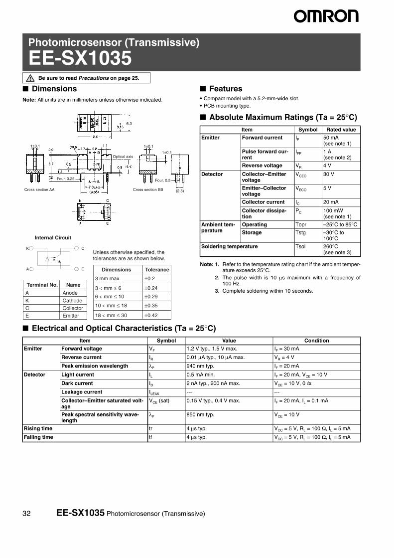
Photomicrosensor (Transmissive)
EE-SX1035Be sure to read Precautions on page 25.
■ DimensionsNote: All units are in millimeters unless otherwise indicated.
■ Features• Compact model with a 5.2-mm-wide slot.• PCB mounting type.
■ Absolute Maximum Ratings (Ta = 25°C)
Note: 1. Refer to the temperature rating chart if the ambient temper-ature exceeds 25°C.
2. The pulse width is 10 μs maximum with a frequency of100 Hz.
3. Complete soldering within 10 seconds.
■ Electrical and Optical Characteristics (Ta = 25°C)
Internal Circuit
K
A
C
E
Terminal No. Name
A Anode
K Cathode
C Collector
E Emitter
Dimensions Tolerance
3 mm max. ±0.2
3 < mm ≤ 6 ±0.24
6 < mm ≤ 10 ±0.29
10 < mm ≤ 18 ±0.35
18 < mm ≤ 30 ±0.42
Cross section AA Cross section BB
Optical axis
Four, 0.5Four, 0.25
1±0.1
1±0.1
1±0.1
(2.5)
6.3
Unless otherwise specified, the tolerances are as shown below.
Item Symbol Rated value
Emitter Forward current IF 50 mA (see note 1)
Pulse forward cur-rent
IFP 1 A (see note 2)
Reverse voltage VR 4 V
Detector Collector–Emitter voltage
VCEO 30 V
Emitter–Collector voltage
VECO 5 V
Collector current IC 20 mA
Collector dissipa-tion
PC 100 mW (see note 1)
Ambient tem-perature
Operating Topr –25°C to 85°CStorage Tstg –30°C to
100°CSoldering temperature Tsol 260°C
(see note 3)
Item Symbol Value Condition
Emitter Forward voltage VF 1.2 V typ., 1.5 V max. IF = 30 mA
Reverse current IR 0.01 μA typ., 10 μA max. VR = 4 V
Peak emission wavelength λP 940 nm typ. IF = 20 mA
Detector Light current IL 0.5 mA min. IF = 20 mA, VCE = 10 V
Dark current ID 2 nA typ., 200 nA max. VCE = 10 V, 0 lx
Leakage current ILEAK --- ---
Collector–Emitter saturated volt-age
VCE (sat) 0.15 V typ., 0.4 V max. IF = 20 mA, IL = 0.1 mA
Peak spectral sensitivity wave-length
λP 850 nm typ. VCE = 10 V
Rising time tr 4 μs typ. VCC = 5 V, RL = 100 Ω, IL = 5 mA
Falling time tf 4 μs typ. VCC = 5 V, RL = 100 Ω, IL = 5 mA
32 EE-SX1035 Photomicrosensor (Transmissive)

■ Engineering Data
Forward Current vs. Collector Dissipation Temperature Rating
Forward Current vs. Forward Voltage Characteristics (Typical)
Light Current vs. Forward Current Characteristics (Typical)
Light Current vs. Collector−Emitter Voltage Characteristics (Typical)
Dark Current vs. Ambient Temperature Characteristics (Typical)
Distance d (mm)
Input
Output
Input
Output
90 %10 %
(Center of optical axis)
Sensing Position Characteristics (Typical)
Response Time Measurement Circuit
Ambient temperature Ta (°C)
Col
lect
or d
issi
patio
n P
C (
mW
)
Forward voltage VF (V)
For
war
d cu
rren
t I F
(m
A)
For
war
d cu
rren
t I F
(m
A)
Forward current IF (mA)
Ligh
t cur
rent
IL
(mA
)
Collector−Emitter voltage VCE (V)
Ligh
t cur
rent
IL
(mA
)
Ambient temperature Ta (°C) Ambient temperature Ta (°C)
Load resistance RL (kΩ)
IF
PC
Ta = −30°C
Ta = 25°C
Ta = 70°C
Ta = 25°CVCE = 10 V
IF = 40 mA
IF = 30 mA
IF = 20 mA
IF = 10 mA
Ta = 25°C VCE = 10 V0 lx
IF = 20 mA VCE = 5 V
IF = 20 mA VCE = 10 V Ta = 25°C
VCC = 5 V Ta = 25°C
Res
pons
e tim
e tr,
tf (
μs)
Rel
ativ
e lig
ht c
urre
nt I
L (%
)
Dar
k cu
rren
t I D
(nA
)
Rel
ativ
e lig
ht c
urre
nt I
L (%
)
IF = 50 mA
Relative Light Current vs. Ambi-ent Temperature Characteristics (Typical)
Response Time vs. Load Resist-ance Characteristics (Typical)
100
80
60
40
20
0−1.5−2.0 −1.0 −0.5 0 0.5 1.0 1.5 2.0
120
d
Distance d (mm)
Sensing Position Characteristics (Typical)
Rel
ativ
e lig
ht c
urre
nt I
L (%
)
IF = 20 mA VCE = 10 V Ta = 25°C
(Cen
ter
of o
ptic
al a
xis)
EE-SX1035 Photomicrosensor (Transmissive) 33
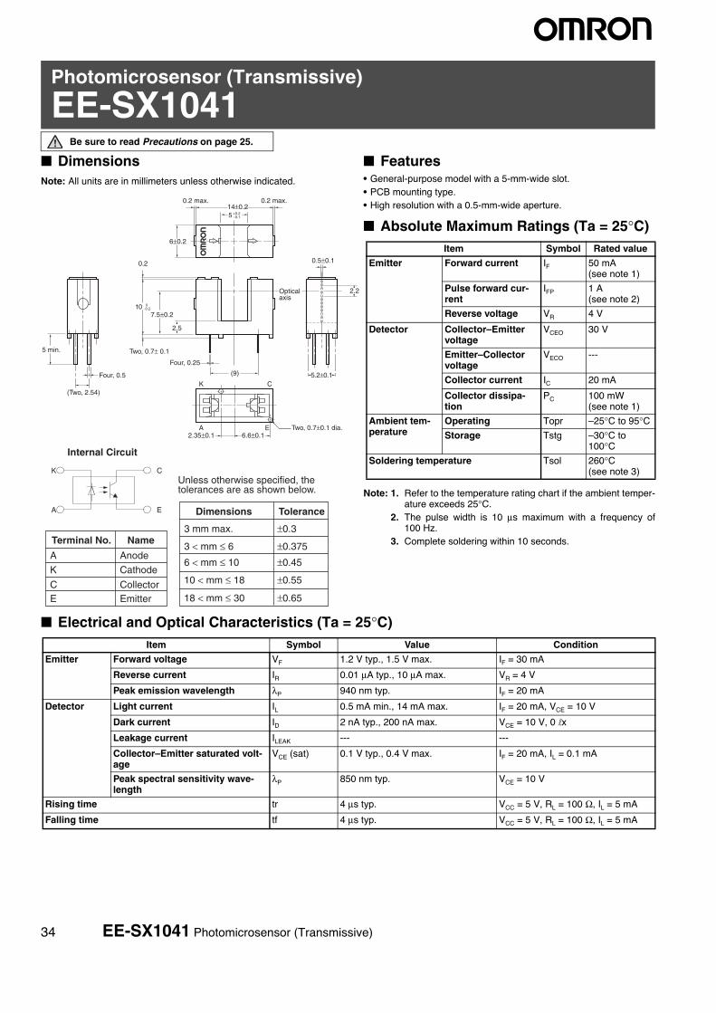
Photomicrosensor (Transmissive)
EE-SX1041Be sure to read Precautions on page 25.
■ DimensionsNote: All units are in millimeters unless otherwise indicated.
■ Features• General-purpose model with a 5-mm-wide slot.• PCB mounting type.• High resolution with a 0.5-mm-wide aperture.
■ Absolute Maximum Ratings (Ta = 25°C)
Note: 1. Refer to the temperature rating chart if the ambient temper-ature exceeds 25°C.
2. The pulse width is 10 μs maximum with a frequency of100 Hz.
3. Complete soldering within 10 seconds.
■ Electrical and Optical Characteristics (Ta = 25°C)
Internal Circuit
K
A
C
E
Terminal No. Name
A Anode
K Cathode
C CollectorE Emitter
Dimensions Tolerance
3 mm max. ±0.3
3 < mm ≤ 6 ±0.375
6 < mm ≤ 10 ±0.45
10 < mm ≤ 18 ±0.55
18 < mm ≤ 30 ±0.65
Unless otherwise specified, the tolerances are as shown below.
Two, 0.7±0.1 dia.
0.2 max. 0.2 max.
5 min.
Optical axis
Two, 0.7± 0.1
Four, 0.25
Four, 0.5
0.5±0.1
5.2±0.1
2.35±0.1
(Two, 2.54)
14±0.2
6.6±0.1
2.2
6±0.2
0.2
7.5±0.2
2.5
K
A E
C
5 +0.2−0.1
10 0−0.2
(9)
Item Symbol Rated value
Emitter Forward current IF 50 mA (see note 1)
Pulse forward cur-rent
IFP 1 A (see note 2)
Reverse voltage VR 4 V
Detector Collector–Emitter voltage
VCEO 30 V
Emitter–Collector voltage
VECO ---
Collector current IC 20 mA
Collector dissipa-tion
PC 100 mW (see note 1)
Ambient tem-perature
Operating Topr –25°C to 95°CStorage Tstg –30°C to
100°CSoldering temperature Tsol 260°C
(see note 3)
Item Symbol Value Condition
Emitter Forward voltage VF 1.2 V typ., 1.5 V max. IF = 30 mA
Reverse current IR 0.01 μA typ., 10 μA max. VR = 4 V
Peak emission wavelength λP 940 nm typ. IF = 20 mA
Detector Light current IL 0.5 mA min., 14 mA max. IF = 20 mA, VCE = 10 V
Dark current ID 2 nA typ., 200 nA max. VCE = 10 V, 0 lx
Leakage current ILEAK --- ---
Collector–Emitter saturated volt-age
VCE (sat) 0.1 V typ., 0.4 V max. IF = 20 mA, IL = 0.1 mA
Peak spectral sensitivity wave-length
λP 850 nm typ. VCE = 10 V
Rising time tr 4 μs typ. VCC = 5 V, RL = 100 Ω, IL = 5 mA
Falling time tf 4 μs typ. VCC = 5 V, RL = 100 Ω, IL = 5 mA
34 EE-SX1041 Photomicrosensor (Transmissive)

■ Engineering Data
Forward Current vs. Collector Dissipation Temperature Rating
Forward Current vs. Forward Voltage Characteristics (Typical)
Light Current vs. Forward Current Characteristics (Typical)
Light Current vs. Collector−Emitter Voltage Characteristics (Typical)
Dark Current vs. Ambient Temperature Characteristics (Typical)
Distance d (mm)
Input
Output
Input
Output
90 %10 %
(Center of optical axis)
Sensing Position Characteristics (Typical)
Response Time Measurement Circuit
Ambient temperature Ta (°C)
Col
lect
or d
issi
patio
n P
C (
mW
)
Forward voltage VF (V)
For
war
d cu
rren
t I F
(m
A)
For
war
d cu
rren
t I F
(m
A)
Forward current IF (mA)
Ligh
t cur
rent
IL
(mA
)Collector−Emitter voltage VCE (V)
Ligh
t cur
rent
IL
(mA
)
Ambient temperature Ta (°C)
Load resistance RL (kΩ)
IF
PC
Ta = −30°C
Ta = 25°C
Ta = 70°C
Ta = 25°CVCE = 10 V
IF = 40 mA
IF = 30 mA
IF = 20 mA
IF = 10 mA
Ta = 25°C VCE = 10 V0 lx
IF = 20 mA VCE = 5 V
IF = 20 mA VCE = 10 V Ta = 25°C
VCC = 5 V Ta = 25°C
Res
pons
e tim
e tr,
tf (
μs)
Rel
ativ
e lig
ht c
urre
nt I
L (%
)
Dar
k cu
rren
t I D
(nA
)
Rel
ativ
e lig
ht c
urre
nt I
L (%
)
IF = 50 mA
Response Time vs. Load Resist-ance Characteristics (Typical)
Relative Light Current vs. Ambi-ent Temperature Characteristics (Typical)
Ambient temperature Ta (°C)
Distance d (mm)
Sensing Position Characteristics (Typical)
Rel
ativ
e lig
ht c
urre
nt I
L (%
)
100
80
60
40
20
0−1.5−2.0 −1.0 −0.5 0 0.5 1.0 1.5 2.0
120
d
IF = 20 mA VCE = 10 V Ta = 25°C
(Cen
ter
of o
ptic
al a
xis)
EE-SX1041 Photomicrosensor (Transmissive) 35

Photomicrosensor (Transmissive)
EE-SX1042Be sure to read Precautions on page 25.
■ DimensionsNote: All units are in millimeters unless otherwise indicated.
■ Features• 14.5-mm-tall model with a deep slot.• PCB mounting type.• High resolution with a 0.5-mm-wide aperture.
■ Absolute Maximum Ratings (Ta = 25°C)
Note: 1. Refer to the temperature rating chart if the ambient temper-ature exceeds 25°C.
2. The pulse width is 10 μs maximum with a frequency of100 Hz.
3. Complete soldering within 10 seconds.
■ Electrical and Optical Characteristics (Ta = 25°C)
Internal Circuit
K
A
C
E
Terminal No. Name
A Anode
K Cathode
C Collector
E Emitter
Dimensions Tolerance
3 mm max. ±0.3
3 < mm ≤ 6 ±0.375
6 < mm ≤ 10 ±0.45
10 < mm ≤ 18 ±0.55
18 < mm ≤ 30 ±0.65
5 min.
Four, C0.3
Four, 0.25
Cross section AA
0.5±0.05
(11.2)(1.92)
14.512±0.4
Unless otherwise specified, the tolerances are as shown below.
Item Symbol Rated value
Emitter Forward current IF 50 mA (see note 1)
Pulse forward cur-rent
IFP 1 A (see note 2)
Reverse voltage VR 4 V
Detector Collector–Emitter voltage
VCEO 30 V
Emitter–Collector voltage
VECO ---
Collector current IC 20 mA
Collector dissipa-tion
PC 100 mW (see note 1)
Ambient tem-perature
Operating Topr –25°C to 85°CStorage Tstg –30°C to 100°C
Soldering temperature Tsol 260°C (see note 3)
Item Symbol Value Condition
Emitter Forward voltage VF 1.2 V typ., 1.5 V max. IF = 30 mA
Reverse current IR 0.01 μA typ., 10 μA max. VR = 4 V
Peak emission wavelength λP 940 nm typ. IF = 20 mA
Detector Light current IL 0.5 mA min., 10 mA max. IF = 20 mA, VCE = 10 V
Dark current ID 2 nA typ., 200 nA max. VCE = 10 V, 0 lx
Leakage current ILEAK --- ---
Collector–Emitter saturated volt-age
VCE (sat) 0.1 V typ., 0.4 V max. IF = 20 mA, IL = 0.1 mA
Peak spectral sensitivity wave-length
λP 850 nm typ. VCE = 10 V
Rising time tr 4 μs typ. VCC = 5 V, RL = 100 Ω, IL = 5 mA
Falling time tf 4 μs typ. VCC = 5 V, RL = 100 Ω, IL = 5 mA
36 EE-SX1042 Photomicrosensor (Transmissive)

■ Engineering Data
Forward Current vs. Collector Dissipation Temperature Rating
Forward Current vs. Forward Voltage Characteristics (Typical)
Light Current vs. Forward Current Characteristics (Typical)
Light Current vs. Collector−Emitter Voltage Characteristics (Typical)
Dark Current vs. Ambient Temperature Characteristics (Typical)
Distance d (mm)
Input
Output
Input
Output
90 %10 %
(Center of optical axis)
Sensing Position Characteristics (Typical)
Response Time Measurement Circuit
Ambient temperature Ta (°C)
Col
lect
or d
issi
patio
n P
C (
mW
)
Forward voltage VF (V)
For
war
d cu
rren
t I F
(m
A)
For
war
d cu
rren
t I F
(m
A)
Forward current IF (mA)
Ligh
t cur
rent
IL
(mA
)Collector−Emitter voltage VCE (V)
Ligh
t cur
rent
IL
(mA
)
Ambient temperature Ta (°C)
Load resistance RL (kΩ)
IF
PCTa = −30°C
Ta = 25°C
Ta = 70°C
Ta = 25°CVCE = 10 V
IF = 40 mA
IF = 30 mA
IF = 20 mA
IF = 10 mA
Ta = 25°C VCE = 10 V0 lx
IF = 20 mA VCE = 5 V
IF = 20 mA VCE = 10 V Ta = 25°C
VCC = 5 V Ta = 25°C
Res
pons
e tim
e tr,
tf (
μs)
Rel
ativ
e lig
ht c
urre
nt I
L (%
)
Dar
k cu
rren
t I D
(nA
)
Rel
ativ
e lig
ht c
urre
nt I
L (%
)
IF = 50 mA
Ambient temperature Ta (°C)
Relative Light Current vs. Ambi-ent Temperature Characteristics (Typical)
Response Time vs. Load Resist-ance Characteristics (Typical)
100
80
60
40
20
0−1.5−2.0 −1.0 −0.5 0 0.5 1.0 1.5 2.0
120
d
Distance d (mm)
Sensing Position Characteristics (Typical)
Rel
ativ
e lig
ht c
urre
nt I
L (%
) IF = 20 mA VCE = 10 V Ta = 25°C
(Cen
ter
of o
ptic
al a
xis)
EE-SX1042 Photomicrosensor (Transmissive) 37

Photomicrosensor (Transmissive)
EE-SX1046Be sure to read Precautions on page 25.
■ DimensionsNote: All units are in millimeters unless otherwise indicated.
■ Features• With a horizontal sensing aperture.• PCB mounting type.• High resolution with a 0.5-mm-wide aperture.
■ Absolute Maximum Ratings (Ta = 25°C)
Note: 1. Refer to the temperature rating chart if the ambient temper-ature exceeds 25°C.
2. The pulse width is 10 μs maximum with a frequency of100 Hz.
3. Complete soldering within 10 seconds.
■ Electrical and Optical Characteristics (Ta = 25°C)
Internal Circuit
K
A
C
E
Terminal No. Name
A Anode
K CathodeC Collector
E Emitter
Dimensions Tolerance
3 mm max. ±0.3
3 < mm ≤ 6 ±0.375
6 < mm ≤ 10 ±0.45
10 < mm ≤ 18 ±0.55
18 < mm ≤ 30 ±0.65
9 min. 0.3 max.Four, 0.25
Optical axis
Cross section BB Cross section AA
Four, 0.25
Optical axis
Optical axis
0.25 max.
0.5±0.110±0.3
0.5±0.1
6.55
2.5
Unless otherwise specified, the tolerances are as shown below.
Item Symbol Rated value
Emitter Forward current IF 50 mA (see note 1)
Pulse forward cur-rent
IFP 1 A (see note 2)
Reverse voltage VR 4 V
Detector Collector–Emitter voltage
VCEO 30 V
Emitter–Collector voltage
VECO ---
Collector current IC 20 mA
Collector dissipa-tion
PC 100 mW (see note 1)
Ambient tem-perature
Operating Topr –25°C to 85°CStorage Tstg –30°C to
100°CSoldering temperature Tsol 260°C
(see note 3)
Item Symbol Value Condition
Emitter Forward voltage VF 1.2 V typ., 1.5 V max. IF = 30 mA
Reverse current IR 0.01 μA typ., 10 μA max. VR = 4 V
Peak emission wavelength λP 920 nm typ. IF = 20 mA
Detector Light current IL 1.2 mA min., 14 mA max. IF = 20 mA, VCE = 5 V
Dark current ID 2 nA typ., 200 nA max. VCE = 10 V, 0 lx
Leakage current ILEAK --- ---
Collector–Emitter saturated volt-age
VCE (sat) 0.1 V typ., 0.4 V max. IF = 20 mA, IL = 0.1 mA
Peak spectral sensitivity wave-length
λP 850 nm typ. VCE = 10 V
Rising time tr 4 μs typ. VCC = 5 V, RL = 100 Ω, IL = 5 mA
Falling time tf 4 μs typ. VCC = 5 V, RL = 100 Ω, IL = 5 mA
38 EE-SX1046 Photomicrosensor (Transmissive)
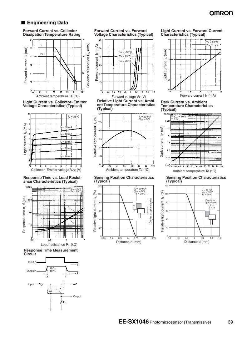
■ Engineering Data
Forward Current vs. Collector Dissipation Temperature Rating
Forward Current vs. Forward Voltage Characteristics (Typical)
Light Current vs. Forward Current Characteristics (Typical)
Light Current vs. Collector−Emitter Voltage Characteristics (Typical)
Dark Current vs. Ambient Temperature Characteristics (Typical)
Input
Output
Input
Output
90 %10 %
Sensing Position Characteristics (Typical)
Response Time Measurement Circuit
Ambient temperature Ta (°C)
Col
lect
or d
issi
patio
n P
C (
mW
)
Forward voltage VF (V)
For
war
d cu
rren
t I F
(m
A)
For
war
d cu
rren
t I F
(m
A)
Forward current IF (mA)
Ligh
t cur
rent
IL
(mA
)Collector−Emitter voltage VCE (V)
Ligh
t cur
rent
IL
(mA
)
Ambient temperature Ta (°C)
Load resistance RL (kΩ)
IF
PCTa = −30°C
Ta = 25°C
Ta = 70°C
Ta = 25°CVCE = 10 V
IF = 40 mA
IF = 30 mA
IF = 20 mA
IF = 10 mA
Ta = 25°C VCE = 10 V0 lx
IF = 20 mA VCE = 5 V
VCC = 5 V Ta = 25°C
Res
pons
e tim
e tr,
tf (
μs)
Rel
ativ
e lig
ht c
urre
nt I
L (%
)
Dar
k cu
rren
t I D
(nA
)IF = 50 mA
Ambient temperature Ta (°C)
Relative Light Current vs. Ambi-ent Temperature Characteristics (Typical)
Response Time vs. Load Resist-ance Characteristics (Typical)
Distance d (mm)
Rel
ativ
e lig
ht c
urre
nt I
L (%
)
100
80
60
40
20
0−0.5−0.75 −0.25 0 0.25 0.5 0.75
120
d
IF = 20 mA VCE = 5 V Ta = 25°C
(Cen
ter
of o
ptic
al a
xis)
Sensing Position Characteristics (Typical)
Distance d (mm)
Rel
ativ
e lig
ht c
urre
nt I
L (%
)
100
80
60
40
20
0−1.5 −1.0 −0.5 0 0.5 1.0 1.5
120
IF = 20 mA VCE = 10 V Ta = 25°C
(Center of optical axis)
d
EE-SX1046 Photomicrosensor (Transmissive) 39

Photomicrosensor (Transmissive)
EE-SX1049Be sure to read Precautions on page 25.
■ DimensionsNote: All units are in millimeters unless otherwise indicated.
■ Features• Compact with a slot width of 2 mm.• PCB mounting type.• High resolution with a 0.5-mm-wide aperture.
■ Absolute Maximum Ratings (Ta = 25°C)
Note: 1. Refer to the temperature rating chart if the ambient temper-ature exceeds 25°C.
2. The pulse width is 10 μs maximum with a frequency of100 Hz.
3. Complete soldering within 10 seconds.
■ Electrical and Optical Characteristics (Ta = 25°C)
Internal Circuit
K
A
C
E
Terminal No. Name
A Anode
K Cathode
C CollectorE Emitter
Dimensions Tolerance
3 mm max. ±0.3
3 < mm ≤ 6 ±0.375
6 < mm ≤ 10 ±0.45
10 < mm ≤ 18 ±0.55
18 < mm ≤ 30 ±0.65
Unless otherwise specified, the tolerances are as shown below.
Cross section BBCross section AA
9
4
Four, C0.3
C0.3
6±0.2
2
A B
A B
1.5
1.5
9 min.
1.2
0.25 max.
2 max.
0.3 max.
K A2.5
0.7±0.1Four, 0.25
E C2.5
2 max.
Four, 0.5
Two, 0.5
Optical axis
Optical axisOptical
axis
Optical axis 5.2 0
−0.2
1.2 dia.0 −0.05
Item Symbol Rated value
Emitter Forward current IF 50 mA (see note 1)
Pulse forward cur-rent
IFP 1 A (see note 2)
Reverse voltage VR 4 V
Detector Collector–Emitter voltage
VCEO 30 V
Emitter–Collector voltage
VECO ---
Collector current IC 20 mA
Collector dissipa-tion
PC 100 mW (see note 1)
Ambient tem-perature
Operating Topr –25°C to 85°CStorage Tstg –30°C to 100°C
Soldering temperature Tsol 260°C (see note 3)
Item Symbol Value Condition
Emitter Forward voltage VF 1.2 V typ., 1.5 V max. IF = 30 mA
Reverse current IR 0.01 μA typ., 10 μA max. VR = 4 V
Peak emission wavelength λP 940 nm typ. IF = 20 mA
Detector Light current IL 0.5 mA min., 14 mA max. IF = 20 mA, VCE = 10 V
Dark current ID 2 nA typ., 200 nA max. VCE = 10 V, 0 lx
Leakage current ILEAK --- ---
Collector–Emitter saturated volt-age
VCE (sat) 0.1 V typ., 0.4 V max. IF = 20 mA, IL = 0.1 mA
Peak spectral sensitivity wave-length
λP 850 nm typ. VCE = 10 V
Rising time tr 4 μs typ. VCC = 5 V, RL = 100 Ω, IL = 5 mA
Falling time tf 4 μs typ. VCC = 5 V, RL = 100 Ω, IL = 5 mA
40 EE-SX1049 Photomicrosensor (Transmissive)

■ Engineering Data
Forward Current vs. Collector Dissipation Temperature Rating
Forward Current vs. Forward Voltage Characteristics (Typical)
Light Current vs. Forward Current Characteristics (Typical)
Light Current vs. Collector−Emitter Voltage Characteristics (Typical)
Dark Current vs. Ambient Temperature Characteristics (Typical)
Distance d (mm)
Input
Output
Input
Output
90 %10 %
Sensing Position Characteristics (Typical)
Response Time Measurement Circuit
Ambient temperature Ta (°C)C
olle
ctor
dis
sipa
tion
PC (
mW
)Forward voltage VF (V)
For
war
d cu
rren
t I F
(m
A)
For
war
d cu
rren
t I F
(m
A)
Forward current IF (mA)
Ligh
t cur
rent
IL
(mA
)Collector−Emitter voltage VCE (V)
Ligh
t cur
rent
IL
(mA
)
Ambient temperature Ta (°C)
Load resistance RL (kΩ)
IF = 20 mA VCE = 10 V Ta = 25°C
Res
pons
e tim
e tr,
tf (
μs)
Rel
ativ
e lig
ht c
urre
nt I
L (%
)
Dar
k cu
rren
t I D
(nA
)
Rel
ativ
e lig
ht c
urre
nt I
L (%
)
Ambient temperature Ta (°C)
60
50
40
30
20
10
0−40 −20 0 20 40 60 80 100
150
100
50
0
PC
IF
60
50
40
30
20
10
00 0.2 0.4 0.6 0.8 1 1.2 1.4 1.6 1.8
Ta = −30°C
Ta = 25°C
Ta = 70°C
0
10
8
6
4
2
010 20 30 40 50
Ta = 25°CVCE = 10 V
0 1 2 3 4 5 6 7 8 9 10
20
18
16
14
12
10
8
6
4
2
120
110
100
90
80
70
60−40 −20 0 20 40 60 80 100
10,000
1,000
100
10
1
0.1
0.01
0.001−30 −20 −10 0 10 20 30 40 50 60 70 80 90
IF = 40 mA
IF = 30 mA
IF = 20 mA
IF = 10 mA
Ta = 25°C IF = 50 mAIF = 20 mA VCE = 10 V
VCE = 10 V0 lx
10,000
0.01
tr
tf
0.1 101
1,000
100
10
1
VCC = 5 V Ta = 25°C
100
80
60
40
20
0−0.5 −0.25 0 0.25 0.5 0.75 1.0
d
120
(Center of optical axis)
tt ft r
t0
VCC
RL
0
IL
Relative Light Current vs. Ambi-ent Temperature Characteristics (Typical)
Response Time vs. Load Resist-ance Characteristics (Typical)
Distance d (mm)
Sensing Position Characteristics (Typical)
Rel
ativ
e lig
ht c
urre
nt I
L (%
)
100
80
60
40
20
0−1.5−2.0 −1.0 −0.5 0 0.5 1.0 1.5 2.0
120
d
IF = 20 mA VCE = 10 V Ta = 25°C
(Cen
ter
of o
ptic
al a
xis)
EE-SX1049 Photomicrosensor (Transmissive) 41

Photomicrosensor (Transmissive)
EE-SX1055Be sure to read Precautions on page 25.
■ DimensionsNote: All units are in millimeters unless otherwise indicated.
■ Features• Longer leads allow the sensor to be mounted to a 1.6-mm thick
board.• 5.4-mm-tall compact model.• PCB mounting type.• High resolution with a 0.5-mm-wide aperture.
■ Absolute Maximum Ratings (Ta = 25°C)
Note: 1. Refer to the temperature rating chart if the ambient temper-ature exceeds 25°C.
2. The pulse width is 10 μs maximum with a frequency of100 Hz.
3. Complete soldering within 10 seconds.
■ Electrical and Optical Characteristics (Ta = 25°C)
Internal Circuit
K
A
C
E
Terminal No. Name
A Anode
K Cathode
C CollectorE Emitter
Dimensions Tolerance
3 mm max. ±0.3
3 < mm ≤ 6 ±0.375
6 < mm ≤ 10 ±0.45
10 < mm ≤ 18 ±0.55
18 < mm ≤ 30 ±0.65
0.2 max. 0.2 max.
Optical axis
Cross section AAFour, 0.5 Four, 0.25
White bandFour, 5° 0.5±0.05
5.4±0.2
3.6±0.5
Unless otherwise specified, the tolerances are as shown below.
Item Symbol Rated value
Emitter Forward current IF 50 mA (see note 1)
Pulse forward cur-rent
IFP 1 A (see note 2)
Reverse voltage VR 4 V
Detector Collector–Emitter voltage
VCEO 30 V
Emitter–Collector voltage
VECO ---
Collector current IC 20 mA
Collector dissipa-tion
PC 100 mW (see note 1)
Ambient tem-perature
Operating Topr –25°C to 85°CStorage Tstg –30°C to 100°C
Soldering temperature Tsol 260°C (see note 3)
Item Symbol Value Condition
Emitter Forward voltage VF 1.2 V typ., 1.5 V max. IF = 30 mA
Reverse current IR 0.01 μA typ., 10 μA max. VR = 4 V
Peak emission wavelength λP 940 nm typ. IF = 20 mA
Detector Light current IL 0.5 mA min., 14 mA max. IF = 20 mA, VCE = 10 V
Dark current ID 2 nA typ., 200 nA max. VCE = 10 V, 0 lx
Leakage current ILEAK --- ---
Collector–Emitter saturated volt-age
VCE (sat) 0.1 V typ., 0.4 V max. IF = 20 mA, IL = 0.1 mA
Peak spectral sensitivity wave-length
λP 850 nm typ. VCE = 10 V
Rising time tr 4 μs typ. VCC = 5 V, RL = 100 Ω, IL = 5 mA
Falling time tf 4 μs typ. VCC = 5 V, RL = 100 Ω, IL = 5 mA
42 EE-SX1055 Photomicrosensor (Transmissive)

■ Engineering Data
Forward Current vs. Collector Dissipation Temperature Rating
Forward Current vs. Forward Voltage Characteristics (Typical)
Light Current vs. Forward Current Characteristics (Typical)
Light Current vs. Collector−Emitter Voltage Characteristics (Typical)
Dark Current vs. Ambient Temperature Characteristics (Typical)
Distance d (mm)
Input
Output
Input
Output
90 %10 %
(Center of optical axis)
Sensing Position Characteristics (Typical)
Response Time Measurement Circuit
Ambient temperature Ta (°C)
Col
lect
or d
issi
patio
n P
C (
mW
)
Forward voltage VF (V)
For
war
d cu
rren
t I F
(m
A)
For
war
d cu
rren
t I F
(m
A)
Forward current IF (mA)
Ligh
t cur
rent
IL
(mA
)Collector−Emitter voltage VCE (V)
Ligh
t cur
rent
IL
(mA
)
Ambient temperature Ta (°C)
Load resistance RL (kΩ)
IF
PC
Ta = −30°C
Ta = 25°C
Ta = 70°C
Ta = 25°CVCE = 10 V
IF = 40 mA
IF = 30 mA
IF = 20 mA
IF = 10 mA
Ta = 25°C VCE = 10 V0 lx
IF = 20 mA VCE = 5 V
IF = 20 mA VCE = 10 V Ta = 25°C
VCC = 5 V Ta = 25°C
Res
pons
e tim
e tr,
tf (
μs)
Rel
ativ
e lig
ht c
urre
nt I
L (%
)
Dar
k cu
rren
t I D
(nA
)
Rel
ativ
e lig
ht c
urre
nt I
L (%
)
IF = 50 mA
Ambient temperature Ta (°C)
Relative Light Current vs. Ambi-ent Temperature Characteristics (Typical)
Response Time vs. Load Resist-ance Characteristics (Typical)
Distance d (mm)
Sensing Position Characteristics (Typical)
Rel
ativ
e lig
ht c
urre
nt I
L (%
)
100
80
60
40
20
0−1.5−2.0 −1.0 −0.5 0 0.5 1.0 1.5 2.0
120
d
IF = 20 mA VCE = 10 V Ta = 25°C
(Cen
ter
of o
ptic
al a
xis)
EE-SX1055 Photomicrosensor (Transmissive) 43

Photomicrosensor (Transmissive)
EE-SX1057Be sure to read Precautions on page 25.
■ DimensionsNote: All units are in millimeters unless otherwise indicated.
■ Features• Compact model with a 3.6-mm-wide slot.• PCB mounting type.
■ Absolute Maximum Ratings (Ta = 25°C)
Note: 1. Refer to the temperature rating chart if the ambient temper-ature exceeds 25°C.
2. The pulse width is 10 μs maximum with a frequency of100 Hz.
3. Complete soldering within 10 seconds.
■ Electrical and Optical Characteristics (Ta = 25°C)
Internal Circuit
K
A
C
E
Terminal No. Name
A AnodeK CathodeC Collector
E Emitter
Dimensions Tolerance
3 mm max. ±0.2
3 < mm ≤ 6 ±0.24
6 < mm ≤ 10 ±0.29
10 < mm ≤ 18 ±0.35
18 < mm ≤ 30 ±0.42
Unless otherwise specified, the tolerances are as shown below.
Item Symbol Rated value
Emitter Forward current IF 50 mA (see note 1)
Pulse forward cur-rent
IFP 1 A (see note 2)
Reverse voltage VR 4 V
Detector Collector–Emitter voltage
VCEO 30 V
Emitter–Collector voltage
VECO 5 V
Collector current IC 20 mA
Collector dissipa-tion
PC 100 mW (see note 1)
Ambient tem-perature
Operating Topr –25°C to 85°CStorage Tstg –30°C to 100°C
Soldering temperature Tsol 260°C (see note 3)
Item Symbol Value Condition
Emitter Forward voltage VF 1.15 V typ., 1.5 V max. IF = 30 mA
Reverse current IR 0.01 μA typ., 10 μA max. VR = 4 V
Peak emission wavelength λP 940 nm typ. IF = 20 mA
Detector Light current IL 1.5 mA min., 8 mA typ., 30 mA max. IF = 15 mA, VCE = 2 V
Dark current ID 2 nA typ., 200 nA max. VCE = 10 V, 0 lx
Leakage current ILEAK --- ---
Collector–Emitter saturated voltage
VCE (sat) 0.4 V max. IF = 30 mA, IL = 1 mA
Peak spectral sensitivity wave-length
λP 850 nm typ. VCE = 10 V
Rising time tr 4 μs typ., 20 μA max. VCC = 10 V, RL = 100 Ω, IL = 5 mA
Falling time tf 4 μs typ., 20 μA max. VCC = 10 V, RL = 100 Ω, IL = 5 mA
44 EE-SX1057 Photomicrosensor (Transmissive)

■ Engineering Data
Forward Current vs. Collector Dissipation Temperature Rating
Forward Current vs. Forward Voltage Characteristics (Typical)
Light Current vs. Forward Current Characteristics (Typical)
Light Current vs. Collector−Emitter Voltage Characteristics (Typical)
Dark Current vs. Ambient Temperature Characteristics (Typical)
Distance d (mm)
Input
Output
Input
Output
90 %10 %
(Center of optical axis)
Sensing Position Characteristics (Typical)
Response Time Measurement Circuit
Ambient temperature Ta (°C)
Col
lect
or d
issi
patio
n P
C (
mW
)
Forward voltage VF (V)
For
war
d cu
rren
t I F
(m
A)
For
war
d cu
rren
t I F
(m
A)
Forward current IF (mA)
Ligh
t cur
rent
IL
(mA
)Collector−Emitter voltage VCE (V)
Ligh
t cur
rent
IL
(mA
)
Ambient temperature Ta (°C)
Load resistance RL (kΩ)
IF
PCTa = −30°C
Ta = 25°C
Ta = 70°C
Ta = 25°CVCE = 10 V
IF = 40 mA
IF = 30 mA
IF = 20 mA
IF = 10 mA
Ta = 25°C VCE = 10 V0 lx
IF = 20 mA VCE = 5 V
IF = 20 mA VCE = 10 V Ta = 25°C
VCC = 5 V Ta = 25°C
Res
pons
e tim
e tr,
tf (
μs)
Rel
ativ
e lig
ht c
urre
nt I
L (%
)
Dar
k cu
rren
t I D
(nA
)
Rel
ativ
e lig
ht c
urre
nt I
L (%
)
IF = 50 mA
Ambient temperature Ta (°C)
Relative Light Current vs. Ambi-ent Temperature Characteristics (Typical)
Response Time vs. Load Resist-ance Characteristics (Typical)
Distance d (mm)
Sensing Position Characteristics (Typical)
Rel
ativ
e lig
ht c
urre
nt I
L (%
)
100
80
60
40
20
0−1.5−2.0 −1.0 −0.5 0 0.5 1.0 1.5 2.0
120
d
IF = 20 mA VCE = 10 V Ta = 25°C
(Cen
ter
of o
ptic
al a
xis)
EE-SX1057 Photomicrosensor (Transmissive) 45

Photomicrosensor (Transmissive)
EE-SX1070Be sure to read Precautions on page 25.
■ DimensionsNote: All units are in millimeters unless otherwise indicated.
■ Features• Wide model with a 8-mm-wide slot.• PCB mounting type.• High resolution with a 0.5-mm-wide aperture.
■ Absolute Maximum Ratings (Ta = 25°C)
Note: 1. Refer to the temperature rating chart if the ambient temper-ature exceeds 25°C.
2. The pulse width is 10 μs maximum with a frequency of100 Hz.
3. Complete soldering within 10 seconds.
■ Electrical and Optical Characteristics (Ta = 25°C)
Internal Circuit
K
A
C
E
Terminal No. NameA Anode
K CathodeC Collector
E Emitter
Dimensions Tolerance
3 mm max. ±0.3
3 < mm ≤ 6 ±0.375
6 < mm ≤ 10 ±0.45
10 < mm ≤ 18 ±0.55
18 < mm ≤ 30 ±0.65
Two, 0.7±0.1
Four, 0.5 Four, 0.25
Two, 0.7±0.1 dia.
0.5±0.1
5.2±0.1
Unless otherwise specified, the tolerances are as shown below.
(13.8)
2.35±0.1
6.6±0.1
8 +0.2−0.1
10 0−0.2
7.5±0.2
2.5
Optical axis
17.7
K
A
C
E
2.2
Two, C1
6.2
(2.5)
(2.5)
JAP
AN
6±0.2
Item Symbol Rated value
Emitter Forward current IF 50 mA (see note 1)
Pulse forward cur-rent
IFP 1 A (see note 2)
Reverse voltage VR 4 V
Detector Collector–Emitter voltage
VCEO 30 V
Emitter–Collector voltage
VECO ---
Collector current IC 20 mA
Collector dissipa-tion
PC 100 mW (see note 1)
Ambient tem-perature
Operating Topr –25°C to 95°CStorage Tstg –30°C to
100°CSoldering temperature Tsol 260°C
(see note 3)
Item Symbol Value Condition
Emitter Forward voltage VF 1.2 V typ., 1.5 V max. IF = 30 mA
Reverse current IR 0.01 μA typ., 10 μA max. VR = 4 V
Peak emission wavelength λP 940 nm typ. IF = 20 mA
Detector Light current IL 0.5 mA min., 14 mA max. IF = 20 mA, VCE = 10 V
Dark current ID 2 nA typ., 200 nA max. VCE = 10 V, 0 lx
Leakage current ILEAK --- ---
Collector–Emitter saturated volt-age
VCE (sat) 0.1 V typ., 0.4 V max. IF = 20 mA, IL = 0.1 mA
Peak spectral sensitivity wave-length
λP 850 nm typ. VCE = 10 V
Rising time tr 4 μs typ. VCC = 5 V, RL = 100 Ω, IL = 5 mA
Falling time tf 4 μs typ. VCC = 5 V, RL = 100 Ω, IL = 5 mA
46 EE-SX1070 Photomicrosensor (Transmissive)

■ Engineering Data
Forward Current vs. Collector Dissipation Temperature Rating
Forward Current vs. Forward Voltage Characteristics (Typical)
Light Current vs. Forward Current Characteristics (Typical)
Light Current vs. Collector−Emitter Voltage Characteristics (Typical)
Dark Current vs. Ambient Temperature Characteristics (Typical)
Distance d (mm)
Input
Output
Input
Output
90 %10 %
(Center of optical axis)
Sensing Position Characteristics (Typical)
Response Time Measurement Circuit
Ambient temperature Ta (°C)
Col
lect
or d
issi
patio
n P
C (
mW
)
Forward voltage VF (V)
For
war
d cu
rren
t I F
(m
A)
For
war
d cu
rren
t I F
(m
A)
Forward current IF (mA)
Ligh
t cur
rent
IL
(mA
)Collector−Emitter voltage VCE (V)
Ligh
t cur
rent
IL
(mA
)
Ambient temperature Ta (°C)
Load resistance RL (kΩ)
IF
PCTa = −30°C
Ta = 25°C
Ta = 70°C
Ta = 25°CVCE = 10 V
IF = 40 mA
IF = 30 mA
IF = 20 mA
IF = 10 mA
Ta = 25°C VCE = 10 V0 lx
IF = 20 mA VCE = 5 V
IF = 20 mA VCE = 10 V Ta = 25°C
VCC = 5 V Ta = 25°C
Res
pons
e tim
e tr,
tf (
μs)
Rel
ativ
e lig
ht c
urre
nt I
L (%
)
Dar
k cu
rren
t I D
(nA
)
Rel
ativ
e lig
ht c
urre
nt I
L (%
)
IF = 50 mA
Ambient temperature Ta (°C)
Relative Light Current vs. Ambi-ent Temperature Characteristics (Typical)
Response Time vs. Load Resist-ance Characteristics (Typical)
60
50
40
30
20
10
0−40 −20 0 20 40 60 80 100
150
100
50
0
Distance d (mm)
Sensing Position Characteristics (Typical)
Rel
ativ
e lig
ht c
urre
nt I
L (%
) 100
80
60
40
20
0−1.5−2.0 −1.0 −0.5 0 0.5 1.0 1.5 2.0
120
d
IF = 20 mA VCE = 10 V Ta = 25°C
(Cen
ter
of o
ptic
al a
xis)
EE-SX1070 Photomicrosensor (Transmissive) 47

Photomicrosensor (Transmissive)
EE-SX1071Be sure to read Precautions on page 25.
■ DimensionsNote: All units are in millimeters unless otherwise indicated.
■ Features• General-purpose model with a 3.4-mm-wide slot.• PCB mounting type.• High resolution with a 0.5-mm-wide aperture.
■ Absolute Maximum Ratings (Ta = 25°C)
Note: 1. Refer to the temperature rating chart if the ambient temper-ature exceeds 25°C.
2. The pulse width is 10 μs maximum with a frequency of100 Hz.
3. Complete soldering within 10 seconds.
■ Electrical and Optical Characteristics (Ta = 25°C)
Internal Circuit
K
A
C
E
Terminal No. Name
A Anode
K CathodeC Collector
E Emitter
Dimensions Tolerance
3 mm max. ±0.3
3 < mm ≤ 6 ±0.375
6 < mm ≤ 10 ±0.45
10 < mm ≤ 18 ±0.55
18 < mm ≤ 30 ±0.65
Four, C0.3
Four, 0.25Four, 0.5
Optical axis
Cross section AA
Cross section BB
(2.54)
10.2
0.20.5
2.1
7.2
6.2
Unless otherwise specified, the tolerances are as shown below.
Item Symbol Rated value
Emitter Forward current IF 50 mA (see note 1)
Pulse forward cur-rent
IFP 1 A (see note 2)
Reverse voltage VR 4 V
Detector Collector–Emitter voltage
VCEO 30 V
Emitter–Collector voltage
VECO ---
Collector current IC 20 mA
Collector dissipa-tion
PC 100 mW (see note 1)
Ambient tem-perature
Operating Topr –25°C to 85°CStorage Tstg –30°C to
100°CSoldering temperature Tsol 260°C
(see note 3)
Item Symbol Value Condition
Emitter Forward voltage VF 1.2 V typ., 1.5 V max. IF = 30 mA
Reverse current IR 0.01 μA typ., 10 μA max. VR = 4 V
Peak emission wavelength λP 940 nm typ. IF = 20 mA
Detector Light current IL 0.5 mA min., 14 mA max. IF = 20 mA, VCE = 10 V
Dark current ID 2 nA typ., 200 nA max. VCE = 10 V, 0 lx
Leakage current ILEAK --- ---
Collector–Emitter saturated volt-age
VCE (sat) 0.1 V typ., 0.4 V max. IF = 20 mA, IL = 0.1 mA
Peak spectral sensitivity wave-length
λP 850 nm typ. VCE = 10 V
Rising time tr 4 μs typ. VCC = 5 V, RL = 100 Ω, IL = 5 mA
Falling time tf 4 μs typ. VCC = 5 V, RL = 100 Ω, IL = 5 mA
48 EE-SX1071 Photomicrosensor (Transmissive)

■ Engineering Data
Forward Current vs. Collector Dissipation Temperature Rating
Forward Current vs. Forward Voltage Characteristics (Typical)
Light Current vs. Forward Current Characteristics (Typical)
Light Current vs. Collector−Emitter Voltage Characteristics (Typical)
Dark Current vs. Ambient Temperature Characteristics (Typical)
Distance d (mm)
Input
Output
Input
Output
90 %10 %
(Center of optical axis)
Sensing Position Characteristics (Typical)
Response Time Measurement Circuit
Ambient temperature Ta (°C)
Col
lect
or d
issi
patio
n P
C (
mW
)
Forward voltage VF (V)
For
war
d cu
rren
t I F
(m
A)
For
war
d cu
rren
t I F
(m
A)
Forward current IF (mA)
Ligh
t cur
rent
IL
(mA
)
Collector−Emitter voltage VCE (V)
Ligh
t cur
rent
IL
(mA
)
Ambient temperature Ta (°C)
Load resistance RL (kΩ)
IF
PCTa = −30°C
Ta = 25°C
Ta = 70°C
Ta = 25°CVCE = 10 V
IF = 40 mA
IF = 30 mA
IF = 20 mA
IF = 10 mA
Ta = 25°C VCE = 10 V0 lx
IF = 20 mA VCE = 5 V
IF = 20 mA VCE = 10 V Ta = 25°C
VCC = 5 V Ta = 25°C
Res
pons
e tim
e tr,
tf (
μs)
Rel
ativ
e lig
ht c
urre
nt I
L (%
)
Dar
k cu
rren
t I D
(nA
)
Rel
ativ
e lig
ht c
urre
nt I
L (%
)
IF = 50 mA
Ambient temperature Ta (°C)
Relative Light Current vs. Ambi-ent Temperature Characteristics (Typical)
Response Time vs. Load Resist-ance Characteristics (Typical)
Distance d (mm)
Sensing Position Characteristics (Typical)
Rel
ativ
e lig
ht c
urre
nt I
L (%
)
100
80
60
40
20
0−1.5−2.0 −1.0 −0.5 0 0.5 1.0 1.5 2.0
120
d
IF = 20 mA VCE = 10 V Ta = 25°C
(Cen
ter
of o
ptic
al a
xis)
EE-SX1071 Photomicrosensor (Transmissive) 49

Photomicrosensor (Transmissive)
EE-SX1081Be sure to read Precautions on page 25.
■ DimensionsNote: All units are in millimeters unless otherwise indicated.
■ Features• General-purpose model with a 5-mm-wide slot.• PCB mounting type.• High resolution with a 0.5-mm-wide aperture.
■ Absolute Maximum Ratings (Ta = 25°C)
Note: 1. Refer to the temperature rating chart if the ambient temper-ature exceeds 25°C.
2. The pulse width is 10 μs maximum with a frequency of100 Hz.
3. Complete soldering within 10 seconds.
■ Electrical and Optical Characteristics (Ta = 25°C)
Internal Circuit
K
A
C
E
Terminal No. NameA Anode
K CathodeC Collector
E Emitter
Dimensions Tolerance
3 mm max. ±0.3
3 < mm ≤ 6 ±0.375
6 < mm ≤ 10 ±0.45
10 < mm ≤ 18 ±0.55
18 < mm ≤ 30 ±0.65
Two, C1±0.3
Four, 0.5±0.1 Four, 0.25±0.1
Four, C0.3
(Optical axis)
Cross section BB Cross section AA
5+0.1
0.5±0.1
8.5±0.1
2.5±0.2
6.2±0.5
10±0.27.5±0.2
13.7±0.3
(10.5)
6.5±0.1
Unless otherwise specified, the tolerances are as shown below.
Item Symbol Rated value
Emitter Forward current IF 50 mA (see note 1)
Pulse forward cur-rent
IFP 1 A (see note 2)
Reverse voltage VR 4 V
Detector Collector–Emitter voltage
VCEO 30 V
Emitter–Collector voltage
VECO ---
Collector current IC 20 mA
Collector dissipa-tion
PC 100 mW (see note 1)
Ambient tem-perature
Operating Topr –25°C to 85°CStorage Tstg –30°C to 100°C
Soldering temperature Tsol 260°C (see note 3)
Item Symbol Value Condition
Emitter Forward voltage VF 1.2 V typ., 1.5 V max. IF = 30 mA
Reverse current IR 0.01 μA typ., 10 μA max. VR = 4 V
Peak emission wavelength λP 940 nm typ. IF = 20 mA
Detector Light current IL 0.5 mA min., 14 mA max. IF = 20 mA, VCE = 10 V
Dark current ID 2 nA typ., 200 nA max. VCE = 10 V, 0 lx
Leakage current ILEAK --- ---
Collector–Emitter saturated volt-age
VCE (sat) 0.1 V typ., 0.4 V max. IF = 20 mA, IL = 0.1 mA
Peak spectral sensitivity wave-length
λP 850 nm typ. VCE = 10 V
Rising time tr 4 μs typ. VCC = 5 V, RL = 100 Ω, IL = 5 mA
Falling time tf 4 μs typ. VCC = 5 V, RL = 100 Ω, IL = 5 mA
50 EE-SX1081 Photomicrosensor (Transmissive)

■ Engineering Data
Forward Current vs. Collector Dissipation Temperature Rating
Forward Current vs. Forward Voltage Characteristics (Typical)
Light Current vs. Forward Current Characteristics (Typical)
Light Current vs. Collector−Emitter Voltage Characteristics (Typical)
Dark Current vs. Ambient Temperature Characteristics (Typical)
Distance d (mm)
Input
Output
Input
Output
90 %10 %
(Center of optical axis)
Sensing Position Characteristics (Typical)
Response Time Measurement Circuit
Ambient temperature Ta (°C)
Col
lect
or d
issi
patio
n P
C (
mW
)
Forward voltage VF (V)
For
war
d cu
rren
t I F
(m
A)
For
war
d cu
rren
t I F
(m
A)
Forward current IF (mA)
Ligh
t cur
rent
IL
(mA
)Collector−Emitter voltage VCE (V)
Ligh
t cur
rent
IL
(mA
)
Ambient temperature Ta (°C)
Load resistance RL (kΩ)
IF
PC
Ta = −30°C
Ta = 25°C
Ta = 70°C
Ta = 25°CVCE = 10 V
IF = 30 mA
IF = 20 mA
IF = 10 mA
Ta = 25°C VCE = 10 V0 lx
IF = 20 mA VCE = 5 V
IF = 20 mA VCE = 10 V Ta = 25°C
VCC = 5 V Ta = 25°C
Res
pons
e tim
e tr,
tf (
μs)
Rel
ativ
e lig
ht c
urre
nt I
L (%
)
Dar
k cu
rren
t I D
(nA
)
Rel
ativ
e lig
ht c
urre
nt I
L (%
)
IF = 50 mA
Ambient temperature Ta (°C)
Relative Light Current vs. Ambi-ent Temperature Characteristics (Typical)
Response Time vs. Load Resist-ance Characteristics (Typical)
IF = 40 mA
Distance d (mm)
Sensing Position Characteristics (Typical)
Rel
ativ
e lig
ht c
urre
nt I
L (%
) 100
80
60
40
20
0−1.5−2.0 −1.0 −0.5 0 0.5 1.0 1.5 2.0
120
d
IF = 20 mA VCE = 10 V Ta = 25°C
(Cen
ter
of o
ptic
al a
xis)
EE-SX1081 Photomicrosensor (Transmissive) 51

Photomicrosensor (Transmissive)
EE-SX1088Be sure to read Precautions on page 25.
■ DimensionsNote: All units are in millimeters unless otherwise indicated.
■ Features• General-purpose model with a 3.4-mm-wide slot.• Mounts to PCBs or connects to connectors.• High resolution with a 0.5-mm-wide aperture.• OMRON’s XK8-series Connectors can be connected without sol-
dering. Contact your OMRON representative for information onobtaining XK8-series Connectors.
■ Absolute Maximum Ratings (Ta = 25°C)
Note: 1. Refer to the temperature rating chart if the ambient temper-ature exceeds 25°C.
2. The pulse width is 10 μs maximum with a frequency of100 Hz.
3. Complete soldering within 10 seconds.
■ Electrical and Optical Characteristics (Ta = 25°C)
Internal Circuit
K
A
C
E
Terminal No. NameA Anode
K CathodeC Collector
E Emitter
Dimensions Tolerance
3 mm max. ±0.3
3 < mm ≤ 6 ±0.375
6 < mm ≤ 10 ±0.45
10 < mm ≤ 18 ±0.55
18 < mm ≤ 30 ±0.65
Two, R1
Two, 3.2±0.2 dia. holes Two, C2Four, C0.3
Four, 0.25Four, 0.5
(Optical axis)
Cross section BB Cross section AA
25±0.219±0.15
0.5±0.1
6.5±0.1
0.5±0.1
8.4±0.1
3±0.4
5±0.2 6±0.2
2.5±0.1
7.2±0.210±0.2
Unless otherwise specified, the tolerances are as shown below.
Item Symbol Rated value
Emitter Forward current IF 50 mA (see note 1)
Pulse forward cur-rent
IFP 1 A (see note 2)
Reverse voltage VR 4 V
Detector Collector–Emitter voltage
VCEO 30 V
Emitter–Collector voltage
VECO ---
Collector current IC 20 mA
Collector dissipa-tion
PC 100 mW (see note 1)
Ambient tem-perature
Operating Topr –25°C to 85°CStorage Tstg –30°C to
100°CSoldering temperature Tsol 260°C
(see note 3)
Item Symbol Value Condition
Emitter Forward voltage VF 1.2 V typ., 1.5 V max. IF = 30 mA
Reverse current IR 0.01 μA typ., 10 μA max. VR = 4 V
Peak emission wavelength λP 940 nm typ. IF = 20 mA
Detector Light current IL 0.5 mA min., 14 mA max. IF = 20 mA, VCE = 10 V
Dark current ID 2 nA typ., 200 nA max. VCE = 10 V, 0 lx
Leakage current ILEAK --- ---
Collector–Emitter saturated volt-age
VCE (sat) 0.15 V typ., 0.4 V max. IF = 20 mA, IL = 0.1 mA
Peak spectral sensitivity wave-length
λP 850 nm typ. VCE = 10 V
Rising time tr 4 μs typ. VCC = 5 V, RL = 100 Ω, IL = 5 mA
Falling time tf 4 μs typ. VCC = 5 V, RL = 100 Ω, IL = 5 mA
52 EE-SX1088 Photomicrosensor (Transmissive)

■ Engineering Data
Forward Current vs. Collector Dissipation Temperature Rating
Forward Current vs. Forward Voltage Characteristics (Typical)
Light Current vs. Forward Current Characteristics (Typical)
Light Current vs. Collector−Emitter Voltage Characteristics (Typical)
Dark Current vs. Ambient Temperature Characteristics (Typical)
Distance d (mm)
Input
Output
Input
Output
90 %10 %
(Center of optical axis)
Sensing Position Characteristics (Typical)
Response Time Measurement Circuit
Ambient temperature Ta (°C)
Col
lect
or d
issi
patio
n P
C (
mW
)
Forward voltage VF (V)
For
war
d cu
rren
t I F
(m
A)
For
war
d cu
rren
t I F
(m
A)
Forward current IF (mA)
Ligh
t cur
rent
IL
(mA
)Collector−Emitter voltage VCE (V)
Ligh
t cur
rent
IL
(mA
)
Ambient temperature Ta (°C)
Load resistance RL (kΩ)
IF
PCTa = −30°C
Ta = 25°C
Ta = 70°C
Ta = 25°CVCE = 10 V
IF = 40 mA
IF = 30 mA
IF = 20 mA
IF = 10 mA
Ta = 25°C VCE = 10 V0 lx
IF = 20 mA VCE = 5 V
IF = 20 mA VCE = 10 V Ta = 25°C
VCC = 5 V Ta = 25°C
Res
pons
e tim
e tr,
tf (
μs)
Rel
ativ
e lig
ht c
urre
nt I
L (%
)
Dar
k cu
rren
t I D
(nA
)
Rel
ativ
e lig
ht c
urre
nt I
L (%
)
IF = 50 mA
Ambient temperature Ta (°C)
Relative Light Current vs. Ambi-ent Temperature Characteristics (Typical)
Response Time vs. Load Resist-ance Characteristics (Typical)
Distance d (mm)
Sensing Position Characteristics (Typical)
Rel
ativ
e lig
ht c
urre
nt I
L (%
) 100
80
60
40
20
0−1.5−2.0 −1.0 −0.5 0 0.5 1.0 1.5 2.0
120
d
IF = 20 mA VCE = 10 V Ta = 25°C
(Cen
ter
of o
ptic
al a
xis)
EE-SX1088 Photomicrosensor (Transmissive) 53
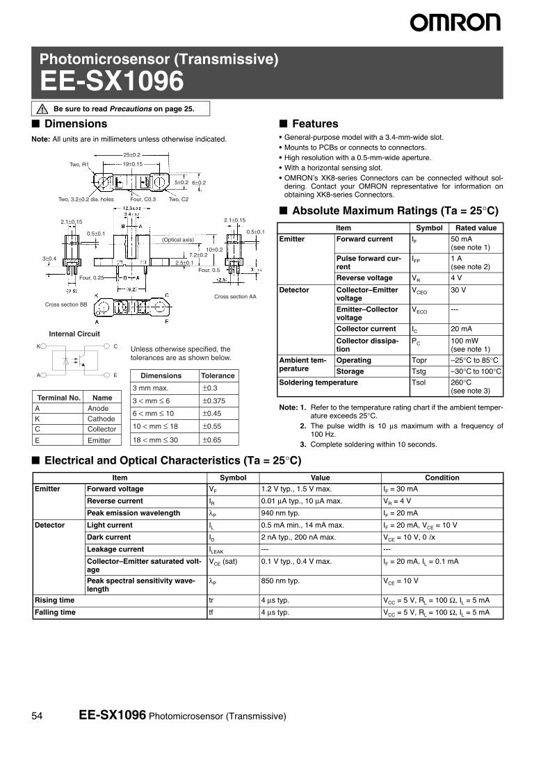
Photomicrosensor (Transmissive)
EE-SX1096Be sure to read Precautions on page 25.
■ DimensionsNote: All units are in millimeters unless otherwise indicated.
■ Features• General-purpose model with a 3.4-mm-wide slot.• Mounts to PCBs or connects to connectors.• High resolution with a 0.5-mm-wide aperture.• With a horizontal sensing slot.• OMRON’s XK8-series Connectors can be connected without sol-
dering. Contact your OMRON representative for information onobtaining XK8-series Connectors.
■ Absolute Maximum Ratings (Ta = 25°C)
Note: 1. Refer to the temperature rating chart if the ambient temper-ature exceeds 25°C.
2. The pulse width is 10 μs maximum with a frequency of100 Hz.
3. Complete soldering within 10 seconds.
■ Electrical and Optical Characteristics (Ta = 25°C)
Internal Circuit
K
A
C
E
Terminal No. NameA Anode
K CathodeC Collector
E Emitter
Dimensions Tolerance
3 mm max. ±0.3
3 < mm ≤ 6 ±0.375
6 < mm ≤ 10 ±0.45
10 < mm ≤ 18 ±0.55
18 < mm ≤ 30 ±0.65
Two, R1
Two, 3.2±0.2 dia. holes Two, C2Four, C0.3
Four, 0.25Four, 0.5
(Optical axis)
Cross section BBCross section AA
25±0.2
19±0.15
0.5±0.1
3±0.4
5±0.2 6±0.2
2.5±0.17.2±0.2
10±0.2
2.1±0.152.1±0.15
0.5±0.1
Unless otherwise specified, the tolerances are as shown below.
Item Symbol Rated value
Emitter Forward current IF 50 mA (see note 1)
Pulse forward cur-rent
IFP 1 A (see note 2)
Reverse voltage VR 4 V
Detector Collector–Emitter voltage
VCEO 30 V
Emitter–Collector voltage
VECO ---
Collector current IC 20 mA
Collector dissipa-tion
PC 100 mW (see note 1)
Ambient tem-perature
Operating Topr –25°C to 85°CStorage Tstg –30°C to 100°C
Soldering temperature Tsol 260°C (see note 3)
Item Symbol Value Condition
Emitter Forward voltage VF 1.2 V typ., 1.5 V max. IF = 30 mA
Reverse current IR 0.01 μA typ., 10 μA max. VR = 4 V
Peak emission wavelength λP 940 nm typ. IF = 20 mA
Detector Light current IL 0.5 mA min., 14 mA max. IF = 20 mA, VCE = 10 V
Dark current ID 2 nA typ., 200 nA max. VCE = 10 V, 0 lx
Leakage current ILEAK --- ---
Collector–Emitter saturated volt-age
VCE (sat) 0.1 V typ., 0.4 V max. IF = 20 mA, IL = 0.1 mA
Peak spectral sensitivity wave-length
λP 850 nm typ. VCE = 10 V
Rising time tr 4 μs typ. VCC = 5 V, RL = 100 Ω, IL = 5 mA
Falling time tf 4 μs typ. VCC = 5 V, RL = 100 Ω, IL = 5 mA
54 EE-SX1096 Photomicrosensor (Transmissive)

■ Engineering Data
Forward Current vs. Collector Dissipation Temperature Rating
Forward Current vs. Forward Voltage Characteristics (Typical)
Light Current vs. Forward Current Characteristics (Typical)
Light Current vs. Collector−Emitter Voltage Characteristics (Typical)
Dark Current vs. Ambient Temperature Characteristics (Typical)
Input
Output
Input
Output
90 %10 %
Sensing Position Characteristics (Typical)
Response Time Measurement Circuit
(Cen
ter
of o
ptic
al a
xis)
d
Ambient temperature Ta (°C)
Col
lect
or d
issi
patio
n P
C (
mW
)
Forward voltage VF (V)
For
war
d cu
rren
t I F
(m
A)
For
war
d cu
rren
t I F
(m
A)
Forward current IF (mA)
Ligh
t cur
rent
IL
(mA
)
Collector−Emitter voltage VCE (V)
Ligh
t cur
rent
IL
(mA
)
Ambient temperature Ta (°C)
Load resistance RL (kΩ)
IF
PC
Ta = −30°C
Ta = 25°C
Ta = 70°C
Ta = 25°CVCE = 10 V
IF = 40 mA
IF = 30 mA
IF = 20 mA
IF = 10 mA
Ta = 25°C VCE = 10 V0 lx
IF = 20 mA VCE = 5 V
IF = 20 mA VCE = 10 V Ta = 25°C
VCC = 5 V Ta = 25°C
Res
pons
e tim
e tr,
tf (
μs)
Rel
ativ
e lig
ht c
urre
nt I
L (%
)
Dar
k cu
rren
t I D
(nA
)
Rel
ativ
e lig
ht c
urre
nt I
L (%
)
IF = 50 mA
Ambient temperature Ta (°C)
Distance d (mm)
Relative Light Current vs. Ambi-ent Temperature Characteristics (Typical)
Response Time vs. Load Resist-ance Characteristics (Typical)
Sensing Position Characteristics (Typical)
Rel
ativ
e lig
ht c
urre
nt I
L (%
)
Distance d (mm)
100
80
60
40
20
0−1.5−2.0 −1.0 −0.5 0 0.5 1.0 1.5 2.0
120
100
80
60
40
20
0−0.5 −0.25 0 0.25 0.5 0.75 1.0
120
d
IF = 20 mA VCE = 10 V Ta = 25°C
(Center of optical axis)
EE-SX1096 Photomicrosensor (Transmissive) 55

Photomicrosensor (Transmissive)
EE-SX1103Be sure to read Precautions on page 25.
■ DimensionsNote: All units are in millimeters unless otherwise indicated.
■ Features• Ultra-compact with a sensor width of 5 mm and a slot width of
2 mm.• PCB mounting type.• High resolution with a 0.4-mm-wide aperture.
■ Absolute Maximum Ratings (Ta = 25°C)
Note: 1. Refer to the temperature rating chart if the ambient temper-ature exceeds 25°C.
2. Complete soldering within 3 seconds.
■ Electrical and Optical Characteristics (Ta = 25°C)
Internal Circuit
Four, 0.5 Four, 0.2
Two, C0.3
Optical axis
Gate
dia.
Two, C0.5
5 min.
Terminal No. Name
A AnodeK Cathode
C CollectorE Emitter
Unless otherwise specified, the tolerances are ±0.2 mm.
Item Symbol Rated value
Emitter Forward current IF 50 mA (see note 1)
Pulse forward cur-rent
IFP ---
Reverse voltage VR 5 V
Detector Collector–Emitter voltage
VCEO 30 V
Emitter–Collector voltage
VECO 4.5 V
Collector current IC 30 mA
Collector dissipa-tion
PC 80 mW (see note 1)
Ambient tem-perature
Operating Topr –25°C to 85°CStorage Tstg –30°C to 100°C
Soldering temperature Tsol 260°C (see note 2)
Item Symbol Value Condition
Emitter Forward voltage VF 1.3 V typ., 1.6 V max. IF = 50 mA
Reverse current IR 10 μA max. VR = 5 V
Peak emission wavelength λP 950 nm typ. IF = 50 mA
Detector Light current IL 0.5 mA min. IF = 20 mA, VCE = 5 V
Dark current ID 500 nA max. VCE = 10 V, 0 lx
Leakage current ILEAK --- ---
Collector–Emitter saturated volt-age
VCE (sat) 0.4 V max. IF = 20 mA, IL = 0.3 mA
Peak spectral sensitivity wave-length
λP 800 nm typ. VCE = 5 V
Rising time tr 10 μs typ. VCC = 5 V, RL = 100 Ω, IF = 20 mA
Falling time tf 10 μs typ. VCC = 5 V, RL = 100 Ω, IF = 20 mA
56 EE-SX1103 Photomicrosensor (Transmissive)

■ Engineering Data
Forward Current vs. Collector Dissipation Temperature Rating
Forward Current vs. Forward Voltage Characteristics (Typical)
Light Current vs. Forward Current Characteristics (Typical)
Light Current vs. Collector−Emitter Voltage Characteristics (Typical)
Dark Current vs. Ambient Temperature Characteristics (Typical)
Sensing Position Characteristics (Typical)
Response Time Measurement Circuit
Input
Output
Input
Output
90 %10 %
Response Time vs. Light Current Characteristics (Typical)
Sensing Position Characteristics (Typical)
VCE = 30 V
VCE = 20 V
VCE = 10 V
Ambient temperature Ta (°C)
Col
lect
or d
issi
patio
n P
C (
mW
)
Forward voltage VF (V)
For
war
d cu
rren
t I F
(m
A)
For
war
d cu
rren
t I F
(m
A)
Forward current IF (mA)
Ligh
t cur
rent
IL
(mA
)
Collector−Emitter voltage VCE (V)
Ligh
t cur
rent
IL
(mA
)
Ambient temperature Ta (°C)
Light current It (mA)
Ta = 25°CVCE = 5 V
IF = 40 mA
IF = 30 mA
IF = 20 mA
IF = 10 mA
Ta = 25°C IF = 20 mA VCE = 5 V
IF = 20 mA VCE = 5 V Ta = 25°C
VCC = 5 V Ta = 25°C
Res
pons
e tim
e tr,
tf (
μs)
Rel
ativ
e lig
ht c
urre
nt I
L (%
)
Dar
k cu
rren
t I D
(nA
)
Rel
ativ
e lig
ht c
urre
nt I
L (%
)
IF = 50 mA
Ambient temperature Ta (°C)
Distance d (mm)
IF = 20 mA VCE = 5 V Ta = 25°C
Rel
ativ
e lig
ht c
urre
nt I
L (%
)
Distance d (mm)
Relative Light Current vs. Ambi-ent Temperature Characteristics (Typical)
EE-SX1103 Photomicrosensor (Transmissive) 57

Photomicrosensor (Transmissive)
EE-SX1105Be sure to read Precautions on page 25.
■ DimensionsNote: All units are in millimeters unless otherwise indicated.
■ Features• Ultra-compact with a sensor width of 4.9 mm and a slot width of
2 mm.• Low-height of 3.3 mm.• PCB mounting type.• High resolution with a 0.4-mm-wide aperture.
■ Absolute Maximum Ratings (Ta = 25°C)
Note: 1. Refer to the temperature rating chart if the ambient tem-perature exceeds 25°C.
2. Complete soldering within 3 seconds.
■ Electrical and Optical Characteristics (Ta = 25°C)
Internal Circuit
Four, 0.5
Two, C0.7
Optical axis
Gate
Four, 0.4 Two, R0.15
Two, R0.3
Cross section AA
Four,
5 min.
Terminal No. NameA Anode
K CathodeC Collector
E Emitter
Unless otherwise specified, the tolerances are ±0.2 mm.
Item Symbol Rated value
Emitter Forward current IF 50 mA (see note 1)
Pulse forward current
IFP ---
Reverse voltage VR 5 V
Detector Collector–Emitter voltage
VCEO 30 V
Emitter–Collector voltage
VECO 4.5 V
Collector current IC 30 mA
Collector dissipation
PC 80 mW (see note 1)
Ambient tem-perature
Operating Topr –25°C to 85°CStorage Tstg –30°C to 85°C
Soldering temperature Tsol 260°C (see note 2)
Item Symbol Value Condition
Emitter Forward voltage VF 1.3 V typ., 1.6 V max. IF = 50 mA
Reverse current IR 10 μA max. VR = 5 V
Peak emission wavelength λP 950 nm typ. IF = 50 mA
Detector Light current IL 0.2 mA min. IF = 20 mA, VCE = 5 V
Dark current ID 500 nA max. VCE = 10 V, 0 lx
Leakage current ILEAK --- ---
Collector–Emitter saturated volt-age
VCE (sat) 0.4 V max. IF = 20 mA, IL = 0.1 mA
Peak spectral sensitivity wave-length
λP 800 nm typ. VCE = 5 V
Rising time tr 10 μs typ. VCC = 5 V, RL = 100 Ω, IF = 20 mA
Falling time tf 10 μs typ. VCC = 5 V, RL = 100 Ω, IF = 20 mA
58 EE-SX1105 Photomicrosensor (Transmissive)

■ Engineering Data
IF = 50 mA
IF = 40 mA
IF = 30 mA
IF = 20 mA
IF = 10 mA
Ta = 25°C
Forward Current vs. Collector Dissipation Temperature Rating
Forward Current vs. Forward Voltage Characteristics (Typical)
Light Current vs. Forward Current Characteristics (Typical)
Light Current vs. Collector−Emitter Voltage Characteristics (Typical)
Dark Current vs. Ambient Temperature Characteristics (Typical)
Sensing Position Characteristics (Typical)
Response Time Measurement Circuit
Input
Output
Input
Output
90 %10 %
Response Time vs. Light Current Characteristics (Typical)
Sensing Position Characteristics (Typical)
Ta = 25°CVCE = 5 V
VCE = 30 V
VCE = 20 V
RL = 1K Ω
RL = 500 Ω
RL = 100 Ω
Ta = 25°CVCE = 5 V
IF = 20 mA VCE = 5 V Ta = 25°C
Ambient temperature Ta (°C)
For
war
d cu
rren
t I F
(m
A)
Forward voltage VF (V) Forward current IF (mA)
Col
lect
or d
issi
patio
n P
c (m
W)
Ambient temperature Ta (°C) Ambient temperature Ta (°C)
Rel
ativ
e lig
ht c
urre
nt I
L (%
)
Collector−Emitter voltage VCE (V)
Distance d (mm)
Res
pons
e tim
e tr,
tf (
μs)
Light current lt (mA)
Ligh
t cur
rent
IL
(mA
)
Rel
ativ
e lig
ht c
urre
nt I
L (%
)
Distance d (mm)
For
war
d cu
rren
t IF (
mA
)
IF = 20 mA VCE = 5 V Ta = 25°C
Rel
ativ
e lig
ht c
urre
nt I
L (%
)D
ark
curr
ent
I D (
nA)
Ligh
t cur
rent
I L (
mA
)
Relative Light Current vs. Ambi-ent Temperature Characteristics (Typical)
2.5
2
1.5
1
0.5
160
140
120
100
80
60
40
20
0−40 −20 0 20 40 60 80 100
IF = 20 mA VCE = 5 V
VCE = 10 V
EE-SX1105 Photomicrosensor (Transmissive) 59

Photomicrosensor (Transmissive)
EE-SX1106Be sure to read Precautions on page 25.
■ DimensionsNote: All units are in millimeters unless otherwise indicated.
■ Features• Ultra-compact with a slot width of 3 mm.• PCB mounting type.• High resolution with a 0.4-mm-wide aperture.
■ Absolute Maximum Ratings (Ta = 25°C)
Note: 1. Refer to the temperature rating chart if the ambient temper-ature exceeds 25°C.
2. Complete soldering within 3 seconds.
■ Electrical and Optical Characteristics (Ta = 25°C)
Internal Circuit
Four, 0.2
Two, C0.7
Optical axis
Gate
Four, 0.5
Two, R1
Two, C0.2
1 0 −0.1dia
1.4 0 −0.1dia
5.4
5 min.
Terminal No. Name
A Anode
K CathodeC Collector
E Emitter
Unless otherwise specified, the tolerances are ±0.2 mm.
Item Symbol Rated value
Emitter Forward current IF 50 mA (see note 1)
Pulse forward cur-rent
IFP ---
Reverse voltage VR 5 V
Detector Collector–Emitter voltage
VCEO 30 V
Emitter–Collector voltage
VECO 4.5 V
Collector current IC 30 mA
Collector dissipa-tion
PC 80 mW (see note 1)
Ambient tem-perature
Operating Topr –25°C to 85°CStorage Tstg –30°C to 85°C
Soldering temperature Tsol 260°C (see note 2)
Item Symbol Value Condition
Emitter Forward voltage VF 1.3 V typ., 1.6 V max. IF = 50 mA
Reverse current IR 10 μA max. VR = 5 V
Peak emission wavelength λP 950 nm typ. IF = 50 mA
Detector Light current IL 0.2 mA min. IF = 20 mA, VCE = 5 V
Dark current ID 500 nA max. VCE = 10 V, 0 lx
Leakage current ILEAK --- ---
Collector–Emitter saturated volt-age
VCE (sat) 0.4 V max. IF = 20 mA, IL = 0.1 mA
Peak spectral sensitivity wave-length
λP 800 nm typ. VCE = 5 V
Rising time tr 10 μs typ. VCC = 5 V, RL = 100 Ω, IF = 20 mA
Falling time tf 10 μs typ. VCC = 5 V, RL = 100 Ω, IF = 20 mA
60 EE-SX1106 Photomicrosensor (Transmissive)

■ Engineering Data
RL = 1K ΩRL = 500 Ω
RL = 100 Ω
Forward Current vs. Collector Dissipation Temperature Rating
Forward Current vs. Forward Voltage Characteristics (Typical)
Light Current vs. Forward Current Characteristics (Typical)
Light Current vs. Collector−Emitter Voltage Characteristics (Typical)
Dark Current vs. Ambient Temperature Characteristics (Typical)
Sensing Position Characteristics (Typical)
Response Time Measurement Circuit
Input
Output
Input
Output
90 %10 %
Response Time vs. Light Current Characteristics (Typical)
Sensing Position Characteristics (Typical)
VCE = 30 V
VCE =20 V
VCE = 10 V
Ambient temperature Ta (°C)
Col
lect
or d
issi
patio
n P
C (
mW
)
Forward voltage VF (V)
For
war
d cu
rren
t I F
(m
A)
For
war
d cu
rren
t I F
(m
A)
Forward current IF (mA)
Ligh
t cur
rent
IL
(mA
)
Collector−Emitter voltage VCE (V)
Ligh
t cur
rent
IL
(mA
)
Ambient temperature Ta (°C)
Light current It (mA)
Ta = 25°CVCE = 5 V
IF = 20 mA
IF = 15 mA
IF = 10 mA
IF = 5 mA
Ta = 25°C IF = 20 mA VCE = 5 V
IF = 20 mA VCE = 5 V Ta = 25°C
VCE = 5 V Ta = 25°C
Res
pons
e tim
e tr,
tf (
μs)
Rel
ativ
e lig
ht c
urre
nt I
L (%
)
Dar
k cu
rren
t I D
(nA
)
Rel
ativ
e lig
ht c
urre
nt I
L (%
)
Ambient temperature Ta (°C)
Distance d (mm)
IF = 20 mA VCE = 5 V Ta = 25°C
Rel
ativ
e lig
ht c
urre
nt I
L (%
)
Distance d (mm)
Relative Light Current vs. Ambi-ent Temperature Characteristics (Typical)
IF = 25 mA
EE-SX1106 Photomicrosensor (Transmissive) 61

Photomicrosensor (Transmissive)
EE-SX1107Be sure to read Precautions on page 25.
■ DimensionsNote: All units are in millimeters unless otherwise indicated.
■ Features• Ultra-compact with a 3.4-mm-wide sensor and a 1-mm-wide slot.• PCB surface mounting type.• High resolution with a 0.15-mm-wide aperture.
■ Absolute Maximum Ratings (Ta = 25°C)
Note: 1. Refer to the temperature rating chart if the ambient temper-ature exceeds 25°C.
2. Duty: 1/100; Pulse width: 0.1 ms3. Complete soldering within 10 seconds for reflow soldering
and within 3 seconds for manual soldering.
■ Electrical and Optical Characteristics (Ta = 25°C)
Internal Circuit
Terminal No. Name
A Anode
K Cathode
C Collector
E Emitter
Recommended Soldering Pattern
Opticalaxis
Cross section AA
Unless otherwise specified, the tolerances are ±0.15 mm.
Item Symbol Rated value
Emitter Forward current IF 25 mA (see note 1)
Pulse forward cur-rent
IFP 100 mA (see note 2)
Reverse voltage VR 5 V
Detector Collector–Emitter voltage
VCEO 20 V
Emitter–Collector voltage
VECO 5 V
Collector current IC 20 mA
Collector dissipa-tion
PC 75 mW (see note 1)
Ambient tem-perature
Operating Topr –30°C to 85°CStorage Tstg –40°C to 90°CReflow soldering Tsol 255°C
(see note 3)
Manual soldering Tsol 350°C(see note 3)
Item Symbol Value Condition
Emitter Forward voltage VF 1.1 V typ., 1.3 V max. IF = 5 mA
Reverse current IR 10 μA max. VR = 5 V
Peak emission wavelength λP 940 nm typ. IF = 20 mA
Detector Light current IL 50 μA min., 150 μA typ., 500 μA max.
IF = 5 mA, VCE = 5 V
Dark current ID 100 nA max. VCE = 10 V, 0 lx
Leakage current ILEAK --- ---
Collector–Emitter saturated voltage VCE (sat) 0.1 V typ., 0.4 V max. IF = 20 mA, IL = 50 μA
Peak spectral sensitivity wavelength λP 900 nm typ. ---
Rising time tr 10 μs typ. VCC = 5 V, RL = 1 kΩ,IL = 100 μA
Falling time tf 10 μs typ. VCC = 5 V, RL = 1 kΩ,IL = 100 μA
62 EE-SX1107 Photomicrosensor (Transmissive)

■ Engineering Data
Forward Current vs. Collector Dissipation Temperature Rating
Forward Current vs. Forward Voltage Characteristics (Typical)
Light Current vs. Forward Current Characteristics (Typical)
Light Current vs. Collector−Emitter Voltage Characteristics (Typical)
Relative Light Current vs. Ambient Temperature Characteristics (Typical)
Dark Current vs. Ambient Tem-perature Characteristics (Typical)
Response Time vs. Load Resistance Characteristics (Typical)
Distance d (mm)
Input
Output
Input
Output
90 %10 %
Sensing Position Characteristics (Typical)
Response Time Measurement Circuit
Distance d (mm)
Sensing Position Character-istics (Typical)
VCE =2 V
VCE = 10 V
Ambient temperature Ta (°C)
Col
lect
or d
issi
patio
n P
C (
mW
)
Forward voltage VF (V)
For
war
d cu
rren
t I F
(m
A)
For
war
d cu
rren
t I F
(m
A)
Forward current IF (mA)
Ligh
t cur
rent
IL
(mA
)Collector−Emitter voltage VCE (V)
Ligh
t cur
rent
IL
(mA
)
Ambient temperature Ta (°C)
Load resistance RL (kΩ)
Ta = 25°CVCE = 5 V
IF = 10 mA
IF = 5 mA
Ta = 25°C IF = 5 mA VCE = 5 V
IF = 5 mA VCE = 5 V
VCC = 5 V Ta = 25°C
Res
pons
e tim
e tr,
tf (
μs)
Rel
ativ
e lig
ht c
urre
nt I
L (%
)
Dar
k cu
rren
t I D
(nA
)
Rel
ativ
e lig
ht c
urre
nt I
L (%
)
Ambient temperature Ta (°C)R
elat
ive
light
cur
rent
IL
(%) IF = 5 mA
VCE = 5 V
EE-SX1107 Photomicrosensor (Transmissive) 63

Unit: mm (inch)
■ Tape and Reel
Reel
Tape
Tape configuration
Tape quantity2,500 pcs./reel
21±0.8 dia.2±0.513±0.5 dia.
80±1 dia.
330±2 dia.
12.4 +20
18.4 max.
Product name
Quantity
Lot number
1.5 dia.
Terminating part (40 mm min.)
Pull-out directionEmpty
(40 mm min.)
Parts mounted Leading part (400 mm min.)
64 EE-SX1107 Photomicrosensor (Transmissive)

Precautions
■ Soldering Information
Reflow soldering• The following soldering paste is recommended:
Melting temperature: 216 to 220°CComposition: Sn 3.5 Ag 0.75 Cu
• The recommended thickness of the metal mask for screen printing is between 0.2 and 0.25 mm.• Set the reflow oven so that the temperature profile shown in the following chart is obtained for the upper surface of the product being soldered.
Manual soldering• Use ”Sn 60” (60% tin and 40% lead) or solder with silver content.• Use a soldering iron of less than 25 W, and keep the temperature of the iron tip at 350°C or below.• Solder each point for a maximum of three seconds.• After soldering, allow the product to return to room temperature before handling it.
StorageTo protect the product from the effects of humidity until the package is opened, dry-box storage is recommended. If this is not possible, store the product under the following conditions:
Temperature: 10 to 30°CHumidity: 60% max.
The product is packed in a humidity-proof envelope. Reflow soldering must be done within 48 hours after opening the envelope, during which time the product must be stored under 30°C at 80% maximum humidity.If it is necessary to store the product after opening the envelope, use dry-box storage or reseal the envelope.
BakingIf a product has remained packed in a humidity-proof envelope for six months or more, or if more than 48 hours have lapsed since the envelope was opened, bake the product under the following conditions before use:
Reel: 60°C for 24 hours or moreBulk: 80°C for 4 hours or more
260°C max.
Time
120 sec
Tem
pera
ture
1 to 5°C/s 150 to 180°C
40 sec max.
10 sec max.
1 to 5°C/s 255°C max.
230°C max.
EE-SX1107 Photomicrosensor (Transmissive) 65

Photomicrosensor (Transmissive)
EE-SX1108Be sure to read Precautions on page 25.
■ DimensionsNote: All units are in millimeters unless otherwise indicated.
■ Features• Ultra-compact with a 5-mm-wide sensor and a 1-mm-wide slot.• PCB surface mounting type.• High resolution with a 0.3-mm-wide aperture.
■ Absolute Maximum Ratings (Ta = 25°C)
Note: 1. Refer to the temperature rating chart if the ambient temper-ature exceeds 25°C.
2. Duty: 1/100; Pulse width: 0.1 ms3. Complete soldering within 10 seconds for reflow soldering
and within 3 seconds for manual soldering.
■ Electrical and Optical Characteristics (Ta = 25°C)
Internal Circuit
Terminal No. Name
A Anode
K CathodeC Collector
E Emitter
Cross section AA
Opticalaxis
Recommended Soldering Pattern
Unless otherwise specified, the tolerances are ±0.15 mm.
Item Symbol Rated value
Emitter Forward current IF 25 mA (see note 1)
Pulse forward cur-rent
IFP 100 mA (see note 2)
Reverse voltage VR 5 V
Detector Collector–Emitter voltage
VCEO 20 V
Emitter–Collector voltage
VECO 5 V
Collector current IC 20 mA
Collector dissipa-tion
PC 75 mW (see note 1)
Ambient tem-perature
Operating Topr –30°C to 85°CStorage Tstg –40°C to 90°CReflow soldering Tsol 255°C
(see note 3)
Manual soldering Tsol 350°C(see note 3)
Item Symbol Value Condition
Emitter Forward voltage VF 1.1 V typ., 1.3 V max. IF = 5 mA
Reverse current IR 10 μA max. VR = 5 V
Peak emission wavelength λP 940 nm typ. IF = 20 mA
Detector Light current IL 50 μA min., 150 μA typ., 500 μA max.
IF = 5 mA, VCE = 5 V
Dark current ID 100 nA max. VCE = 10 V, 0 lx
Leakage current ILEAK --- ---
Collector–Emitter saturated voltage VCE (sat) 0.1 V typ., 0.4 V max. IF = 20 mA, IL = 50 μA
Peak spectral sensitivity wavelength λP 900 nm typ. ---
Rising time tr 10 μs typ. VCC = 5 V, RL = 1 kΩ,IL = 100 μA
Falling time tf 10 μs typ. VCC = 5 V, RL = 1 kΩ,IL = 100 μA
66 EE-SX1108 Photomicrosensor (Transmissive)

■ Engineering Data
Forward Current vs. Collector Dissipation Temperature Rating
Forward Current vs. Forward Voltage Characteristics (Typical)
Light Current vs. Forward Current Characteristics (Typical)
Light Current vs. Collector−Emitter Voltage Characteristics (Typical)
Relative Light Current vs. Ambient Temperature Characteristics (Typical)
Dark Current vs. Ambient Tem-perature Characteristics (Typical)
Distance d (mm)
Input
Output
Input
Output
90 %10 %
Sensing Position Characteristics (Typical)
Response Time Measurement Circuit
Distance d (mm)
Sensing Position Characteristics (Typical)
VCE = 2 V
Ambient temperature Ta (°C)
Col
lect
or d
issi
patio
n P
C (
mW
)
Forward voltage VF (V)
For
war
d cu
rren
t I F
(m
A)
For
war
d cu
rren
t I F
(m
A)
Forward current IF (mA)
Ligh
t cur
rent
IL
(mA
)Collector−Emitter voltage VCE (V)
Ligh
t cur
rent
IL
(mA
)
Ambient temperature Ta (°C)
Load resistance RL (kΩ)
Ta = 25°CVCE = 5 V
IF = 10 mA
IF = 5 mA
Ta = 25°CIF = 5 mA VCE = 5 V
IF = 5 mA VCE = 5 V
VCC = 5 V Ta = 25°C
Res
pons
e tim
e tr,
tf (
μs)
Rel
ativ
e lig
ht c
urre
nt I
L (%
)
Dar
k cu
rren
t I D
(nA
)
Rel
ativ
e lig
ht c
urre
nt I
L (%
)
Ambient temperature Ta (°C)
Rel
ativ
e lig
ht c
urre
nt I
L (%
) IF = 5 mA VCE = 5 V
Response Time vs. Load Resist-ance Characteristics (Typical)
VCE = 10 V
EE-SX1108 Photomicrosensor (Transmissive) 67

Unit: mm (inch)
■ Tape and Reel
Reel
Tape
Tape configuration
Tape quantity2,000 pcs./reel
21±0.8 dia.2±0.5
13±0.5 dia.
Product name
Quantity
Lot number
80±1 dia.
330±2 dia.
12.4+20
18.4 max.
1.5 dia.
Terminating part (40 mm min.)
Pull-out directionEmpty
(40 mm min.)
Parts mounted Leading part (400 mm min.)
68 EE-SX1108 Photomicrosensor (Transmissive)

Precautions
■ Soldering Information
Reflow soldering• The following soldering paste is recommended:
Melting temperature: 216 to 220°CComposition: Sn 3.5 Ag 0.75 Cu
• The recommended thickness of the metal mask for screen printing is between 0.2 and 0.25 mm.• Set the reflow oven so that the temperature profile shown in the following chart is obtained for the upper surface of the product being soldered.
Manual soldering• Use ”Sn 60” (60% tin and 40% lead) or solder with silver content.• Use a soldering iron of less than 25 W, and keep the temperature of the iron tip at 300°C or below.• Solder each point for a maximum of three seconds.• After soldering, allow the product to return to room temperature before handling it.
StorageTo protect the product from the effects of humidity until the package is opened, dry-box storage is recommended. If this is not possible, store the product under the following conditions:
Temperature: 10 to 30°CHumidity: 60% max.
The product is packed in a humidity-proof envelope. Reflow soldering must be done within 48 hours after opening the envelope, during which time the product must be stored under 30°C at 80% maximum humidity.If it is necessary to store the product after opening the envelope, use dry-box storage or reseal the envelope.
BakingIf a product has remained packed in a humidity-proof envelope for six months or more, or if more than 48 hours have lapsed since the envelope was opened, bake the product under the following conditions before use:
Reel: 60°C for 24 hours or moreBulk: 80°C for 4 hours or more
260°C max.
Time
120 sec
Tem
pera
ture
1 to 5°C/s 150 to 180°C
40 sec max.
10 sec max.
1 to 5°C/s 255°C max.
230°C max.
EE-SX1108 Photomicrosensor (Transmissive) 69

Photomicrosensor (Transmissive)
EE-SX1109Be sure to read Precautions on page 25.
■ DimensionsNote: All units are in millimeters unless otherwise indicated.
■ Features• Ultra-compact with a 6-mm-wide sensor and a 3-mm-wide slot.• PCB surface mounting type.• High resolution with a 0.5-mm-wide aperture.
■ Absolute Maximum Ratings (Ta = 25°C)
Note: 1. Refer to the temperature rating chart if the ambient temper-ature exceeds 25°C.
2. Duty: 1/100; Pulse width: 0.1 ms3. Complete soldering within 10 seconds for reflow soldering
and within 3 seconds for manual soldering.
■ Electrical and Optical Characteristics (Ta = 25°C)
Internal Circuit
Terminal No. Name
A Anode
K CathodeC Collector
E Emitter
Recommended Soldering Pattern
Opticalaxis
Cross section AA
Unless otherwise specified, the tolerances are ±0.15 mm.
Item Symbol Rated value
Emitter Forward current IF 25 mA (see note 1)
Pulse forward cur-rent
IFP 100 mA (see note 2)
Reverse voltage VR 5 V
Detector Collector–Emitter voltage
VCEO 20 V
Emitter–Collector voltage
VECO 5 V
Collector current IC 20 mA
Collector dissipa-tion
PC 75 mW (see note 1)
Ambient tem-perature
Operating Topr –30°C to 85°CStorage Tstg –40°C to 90°CReflow soldering Tsol 255°C
(see note 3)
Manual soldering Tsol 350°C(see note 3)
Item Symbol Value Condition
Emitter Forward voltage VF 1.1 V typ., 1.3 V max. IF = 5 mA
Reverse current IR 10 μA max. VR = 5 V
Peak emission wavelength λP 940 nm typ. IF = 20 mA
Detector Light current IL 50 μA min., 150 μA typ., 500 μA max.
IF = 5 mA, VCE = 5 V
Dark current ID 100 nA max. VCE = 10 V, 0 lx
Leakage current ILEAK --- ---
Collector–Emitter saturated volt-age
VCE (sat) 0.1 V typ., 0.4 V max. IF = 20 mA, IL = 50 μA
Peak spectral sensitivity wave-length
λP 900 nm typ. ---
Rising time tr 10 μs typ. VCC = 5 V, RL = 1 kΩ,IL = 100 μA
Falling time tf 10 μs typ. VCC = 5 V, RL = 1 kΩ,IL = 100 μA
70 EE-SX1109 Photomicrosensor (Transmissive)

■ Engineering DataForward Current vs. Collector Dis-sipation Temperature Rating
Forward Current vs. Forward Voltage Characteristics (Typical)
Light Current vs. Forward Current Characteristics (Typical)
Light Current vs. Collector−Emitter Voltage Characteristics (Typical)
Relative Light Current vs. Ambient Temperature Characteristics (Typical)
Input
Output
Input
Output
90 %10 %
Sensing Position Characteris-tics (Typical)
Response Time Measurement Circuit
Sensing Position Characteris-tics (Typical)
Distance d (mm) Distance d (mm)
VCE = 2 V
VCE = 10 V
Ambient temperature Ta (°C)
Col
lect
or d
issi
patio
n P
C (
mW
)
Forward voltage VF (V)
For
war
d cu
rren
t I F
(m
A)
For
war
d cu
rren
t I F
(m
A)
Forward current IF (mA)
Ligh
t cur
rent
IL
(mA
)
Collector−Emitter voltage VCE (V)
Ligh
t cur
rent
IL
(mA
)
Ambient temperature Ta (°C)
Load resistance RL (kΩ)
Ta = 25°CVCE = 5 V
IF = 10 mA
IF = 5 mA
Ta = 25°C IF = 5 mA VCE = 5 V
IF = 5 mA VCE = 5 V
VCC = 5 V Ta = 25°C
Res
pons
e tim
e tr,
tf (
μs)
Rel
ativ
e lig
ht c
urre
nt I
L (%
)
Dar
k cu
rren
t I D
(nA
)
Rel
ativ
e lig
ht c
urre
nt I
L (%
)
Ambient temperature Ta (°C)
Rel
ativ
e lig
ht c
urre
nt I
L (%
) IF = 5 mA VCE = 5 V
Response Time vs. Load Resist-ance Characteristics (Typical)
Dark Current vs. Ambient Temper-ature Characteristics (Typical)
EE-SX1109 Photomicrosensor (Transmissive) 71

Unit: mm (inch)
■ Tape and Reel
Reel
Tape
Tape configuration
Tape quantity1,000 pcs./reel
21±0.8 dia.2±0.5
13±0.5 dia.
Product name
Quantity
Lot No.
80±1 dia.
330+2 dia.
12.4+20
18.4 max.
1.5 dia.
Terminating part (40 mm min.)
Pull-out directionEmpty
(40 mm min.)
Parts mounted Leading part (400 mm min.)
72 EE-SX1109 Photomicrosensor (Transmissive)

Precautions
■ Soldering Information
Reflow soldering• The following soldering paste is recommended:
Melting temperature: 216 to 220°CComposition: Sn 3.5 Ag 0.75 Cu
• The recommended thickness of the metal mask for screen printing is between 0.2 and 0.25 mm.• Set the reflow oven so that the temperature profile shown in the following chart is obtained for the upper surface of the product being soldered.
Manual soldering• Use ”Sn 60” (60% tin and 40% lead) or solder with silver content.• Use a soldering iron of less than 25 W, and keep the temperature of the iron tip at 300°C or below.• Solder each point for a maximum of three seconds.• After soldering, allow the product to return to room temperature before handling it.
StorageTo protect the product from the effects of humidity until the package is opened, dry-box storage is recommended. If this is not possible, store the product under the following conditions:
Temperature: 10 to 30°CHumidity: 60% max.
The product is packed in a humidity-proof envelope. Reflow soldering must be done within 48 hours after opening the envelope, during which time the product must be stored under 30°C at 80% maximum humidity.If it is necessary to store the product after opening the envelope, use dry-box storage or reseal the envelope.
BakingIf a product has remained packed in a humidity-proof envelope for six months or more, or if more than 48 hours have lapsed since the envelope was opened, bake the product under the following conditions before use:
Reel: 60°C for 24 hours or moreBulk: 80°C for 4 hours or more
260°C max.
Time
120 sec
Tem
pera
ture
1 to 5°C/s 150 to 180°C
40 sec max.
10 sec max.
1 to 5°C/s 255°C max.
230°C max.
EE-SX1109 Photomicrosensor (Transmissive) 73

Photomicrosensor (Transmissive)
EE-SX1115Be sure to read Precautions on page 25.
■ DimensionsNote: All units are in millimeters unless otherwise indicated.
■ Features• 14.5-mm-tall model with a deep slot.• PCB mounting type.• High resolution with a 0.5-mm-wide aperture.
■ Absolute Maximum Ratings (Ta = 25°C)
Note: 1. Refer to the temperature rating chart if the ambient temper-ature exceeds 25°C.
2. The pulse width is 10 μs maximum with a frequency of100 Hz.
3. Complete soldering within 10 seconds.
■ Electrical and Optical Characteristics (Ta = 25°C)
Internal Circuit
K
A
C
E
Terminal No. Name
A AnodeK Cathode
C Collector
E Emitter
Dimensions Tolerance
3 mm max. ±0.3
3 < mm ≤ 6 ±0.375
6 < mm ≤ 10 ±0.45
10 < mm ≤ 18 ±0.55
18 < mm ≤ 30 ±0.65
Unless otherwise specified, the tolerances are as shown below.
Cross section AA
0.5±0.05
12±0.4
Four, 0.5
(1.94)
Optical axis
(2.1)4.2±0.1
K
A
C
E
CB
(11.2)
Four, 0.25
2-25 min.A
2.5
14.5
0.2 5
14
A
Four, C0.3
5
1.03
1.03
Four, R0.1
Four, R0.1
1.35+0.06−0.01 1.35+0.06
−0.01
1.35+0.06−0.01
1.35+0.06−0.01
Part B
Part C
Item Symbol Rated value
Emitter Forward current IF 50 mA (see note 1)
Pulse forward cur-rent
IFP 1 A (see note 2)
Reverse voltage VR 4 V
Detector Collector–Emitter voltage
VCEO 30 V
Emitter–Collector voltage
VECO ---
Collector current IC 20 mA
Collector dissipa-tion
PC 100 mW (see note 1)
Ambient tem-perature
Operating Topr –25°C to 85°CStorage Tstg –30°C to
100°CSoldering temperature Tsol 260°C
(see note 3)
Item Symbol Value Condition
Emitter Forward voltage VF 1.2 V typ., 1.5 V max. IF = 30 mA
Reverse current IR 0.01 μA typ., 10 μA max. VR = 4 V
Peak emission wavelength λP 940 nm typ. IF = 20 mA
Detector Light current IL 0.5 mA min., 14 mA max. IF = 20 mA, VCE = 10 V
Dark current ID 2 nA typ., 200 nA max. VCE = 10 V, 0 lx
Leakage current ILEAK --- ---
Collector–Emitter saturated volt-age
VCE (sat) 0.1 V typ., 0.4 V max. IF = 20 mA, IL = 0.1 mA
Peak spectral sensitivity wave-length
λP 850 nm typ. VCE = 10 V
Rising time tr 4 μs typ. VCC = 5 V, RL = 100 Ω, IL = 5 mA
Falling time tf 4 μs typ. VCC = 5 V, RL = 100 Ω, IL = 5 mA
74 EE-SX1115 Photomicrosensor (Transmissive)

■ Engineering Data
Forward Current vs. Collector Dissipation Temperature Rating
Forward Current vs. Forward Voltage Characteristics (Typical)
Light Current vs. Forward Current Characteristics (Typical)
Light Current vs. Collector−Emitter Voltage Characteristics (Typical)
Dark Current vs. Ambient Temperature Characteristics (Typical)
Distance d (mm)
Input
Output
Input
Output
90 %10 %
(Center of optical axis)
Sensing Position Characteristics (Typical)
Response Time Measurement Circuit
Ambient temperature Ta (°C)
Col
lect
or d
issi
patio
n P
C (
mW
)
Forward voltage VF (V)
For
war
d cu
rren
t I F
(m
A)
For
war
d cu
rren
t I F
(m
A)
Forward current IF (mA)
Ligh
t cur
rent
IL
(mA
)Collector−Emitter voltage VCE (V)
Ligh
t cur
rent
IL
(mA
)
Ambient temperature Ta (°C)
Load resistance RL (kΩ)
IF
PCTa = −30°C
Ta = 25°C
Ta = 70°C
Ta = 25°CVCE = 10 V
IF = 40 mA
IF = 30 mA
IF = 20 mA
IF = 10 mA
Ta = 25°C VCE = 10 V0 lx
IF = 20 mA VCE = 5 V
IF = 20 mA VCE = 10 V Ta = 25°C
VCC = 5 V Ta = 25°C
Res
pons
e tim
e tr,
tf (
μs)
Rel
ativ
e lig
ht c
urre
nt I
L (%
)
Dar
k cu
rren
t I D
(nA
)
Rel
ativ
e lig
ht c
urre
nt I
L (%
)
IF = 50 mA
Ambient temperature Ta (°C)
Relative Light Current vs. Ambi-ent Temperature Characteristics (Typical)
Response Time vs. Load Resist-ance Characteristics (Typical)
Distance d (mm)
Sensing Position Characteristics (Typical)
Rel
ativ
e lig
ht c
urre
nt I
L (%
)
100
80
60
40
20
0−1.5−2.0 −1.0 −0.5 0 0.5 1.0 1.5 2.0
120
d
IF = 20 mA VCE = 10 V Ta = 25°C
(Cen
ter
of o
ptic
al a
xis)
EE-SX1115 Photomicrosensor (Transmissive) 75

Photomicrosensor (Transmissive)
EE-SX1128Be sure to read Precautions on page 25.
■ DimensionsNote: All units are in millimeters unless otherwise indicated.
■ Features• General-purpose model with a 4.2-mm-wide slot.• PCB mounting type.• High resolution with a 0.5-mm-wide aperture.• Horizontal sensing aperture.
■ Absolute Maximum Ratings (Ta = 25°C)
Note: 1. Refer to the temperature rating chart if the ambient temper-ature exceeds 25°C.
2. The pulse width is 10 μs maximum with a frequency of100 Hz.
3. Complete soldering within 10 seconds.
■ Electrical and Optical Characteristics (Ta = 25°C)
Internal Circuit
K
A
C
E
Terminal No. Name
A AnodeK Cathode
C Collector
E Emitter
Dimensions Tolerance
0 < × ≤ 4 ±0.100
4 < × ≤ 18 ±0.200
Unless otherwise specified, the tolerances are as shown below.
Item Symbol Rated value
Emitter Forward current IF 50 mA (see note 1)
Pulse forward cur-rent
IFP 1 A (see note 2)
Reverse voltage VR 4 V
Detector Collector–Emitter voltage
VCEO 30 V
Emitter–Collector voltage
VECO ---
Collector current IC 20 mA
Collector dissipa-tion
PC 100 mW (see note 1)
Ambient tem-perature
Operating Topr –25°C to 85°CStorage Tstg –30°C to
100°CSoldering temperature Tsol 260°C
(see note 3)
Item Symbol Value Condition
Emitter Forward voltage VF 1.2 V typ., 1.5 V max. IF = 30 mA
Reverse current IR 0.01 μA typ., 10 μA max. VR = 4 V
Peak emission wavelength λP 940 nm typ. IF = 20 mA
Detector Light current IL 0.5 mA min., 10 mA max. IF = 20 mA, VCE = 10 V
Dark current ID 2 nA typ., 200 nA max. VCE = 10 V, 0 lx
Leakage current ILEAK --- ---
Collector–Emitter saturated volt-age
VCE (sat) 0.1 V typ., 0.4 V max. IF = 20 mA, IL = 0.1 mA
Peak spectral sensitivity wave-length
λP 850 nm typ. VCE = 10 V
Rising time tr 4 μs typ. VCC = 5 V, RL = 100 Ω, IL = 5 mA
Falling time tf 4 μs typ. VCC = 5 V, RL = 100 Ω, IL = 5 mA
76 EE-SX1128 Photomicrosensor (Transmissive)
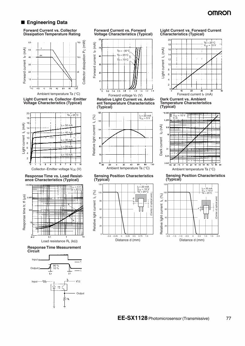
■ Engineering Data
Forward Current vs. Collector Dissipation Temperature Rating
Forward Current vs. Forward Voltage Characteristics (Typical)
Light Current vs. Forward Current Characteristics (Typical)
Light Current vs. Collector−Emitter Voltage Characteristics (Typical)
Dark Current vs. Ambient Temperature Characteristics (Typical)
Distance d (mm)
Input
Output
Input
Output
90 %10 %
d
Sensing Position Characteristics (Typical)
Response Time Measurement Circuit
20
18
16
14
12
10
8
6
4
2
20
18
16
14
12
10
8
6
4
2
Ambient temperature Ta (°C)
Col
lect
or d
issi
patio
n P
C (
mW
)
Forward voltage VF (V)
For
war
d cu
rren
t I F
(m
A)
For
war
d cu
rren
t I F
(m
A)
Forward current IF (mA)
Ligh
t cur
rent
IL
(mA
)
Collector−Emitter voltage VCE (V)
Ligh
t cur
rent
IL
(mA
)
Ambient temperature Ta (°C)
Load resistance RL (kΩ)
Ta = −30°C
Ta = 25°C
Ta = 70°C
Ta = 25°CVCE = 10 V
IF = 40 mA
IF = 30 mA
IF = 20 mA
IF = 10 mA
Ta = 25°C VCE = 10 V0 lx
IF = 20 mA VCE = 5 V
IF = 20 mA VCE = 10 V Ta = 25°C
VCC = 5 V Ta = 25°C
Res
pons
e tim
e tr,
tf (
μs)
Rel
ativ
e lig
ht c
urre
nt I
L (%
)
Dar
k cu
rren
t I D
(nA
)
Rel
ativ
e lig
ht c
urre
nt I
L (%
)
IF = 50 mA
Ambient temperature Ta (°C)
Relative Light Current vs. Ambi-ent Temperature Characteristics (Typical)
Response Time vs. Load Resist-ance Characteristics (Typical)
Distance d (mm)
Sensing Position Characteristics (Typical)
Rel
ativ
e lig
ht c
urre
nt I
L (%
) 100
80
60
40
20
0−1.5−2.0 −1.0 −0.5 0 0.5 1.0 1.5 2.0
120
d
IF = 20 mA VCE = 10 V Ta = 25°C 100
80
60
40
20
0−0.5 −0.25 0 0.25 0.5 0.75 1.0
120
(Cen
ter
of o
ptic
al a
xis)
(Cen
ter
of o
ptic
al a
xis)
EE-SX1128 Photomicrosensor (Transmissive) 77

Photomicrosensor (Transmissive)
EE-SX1131Be sure to read Precautions on page 25.
■ DimensionsNote: All units are in millimeters unless otherwise indicated.
■ Features• Ultra-compact with a 5-mm-wide sensor and a 2-mm-wide slot.• PCB surface mounting type.• High resolution with a 0.3-mm-wide aperture.• Dual-channel output.
■ Absolute Maximum Ratings (Ta = 25°C)
Note: 1. Refer to the temperature rating chart if the ambient temper-ature exceeds 25°C.
2. Duty: 1/100; Pulse width: 0.1 ms3. Complete soldering within 10 seconds for reflow soldering
and within 3 seconds for manual soldering.
■ Electrical and Optical Characteristics (Ta = 25°C)
Internal Circuit
Terminal No. Name
A Anode
NC Not connected.K CathodeC Collector
E1 Emitter 1E2 Emitter 2
Recommended Soldering Pattern
Cross section AA
Opticalaxis
Unless otherwise specified, the tolerances are ±0.15 mm.
Item Symbol Rated value
Emitter Forward current IF 25 mA (see note 1)
Pulse forward cur-rent
IFP 100 mA (see note 2)
Reverse voltage VR 5 V
Detector Collector–Emitter voltage
VCEO 20 V
Emitter–Collector voltage
VECO 5 V
Collector current IC 20 mA
Collector dissipa-tion
PC 75 mW (see note 1)
Ambient tem-perature
Operating Topr –30°C to 85°CStorage Tstg –40°C to 90°CReflow soldering Tsol 255°C
(see note 3)
Manual soldering Tsol 350°C(see note 3)
Item Symbol Value Condition
Emitter Forward voltage VF 1.1 V typ., 1.3 V max. IF = 5 mA
Reverse current IR 10 μA max. VR = 5 V
Peak emission wavelength λP 940 nm typ. IF = 20 mA
Detector Light current IL1/IL2 50 μA min., 150 μA typ., 500 μA max.
IF = 5 mA, VCE = 5 V
Dark current ID 100 nA max. VCE = 10 V, 0 lx
Leakage current ILEAK --- ---
Collector–Emitter saturated voltage VCE (sat) 0.1 V typ., 0.4 V max. IF = 20 mA, IL = 50 μA
Peak spectral sensitivity wavelength λP 900 nm typ. ---
Rising time tr 10 μs typ. VCC = 5 V, RL = 1 kΩ,IL = 100 μA
Falling time tf 10 μs typ. VCC = 5 V, RL = 1 kΩ,IL = 100 μA
78 EE-SX1131 Photomicrosensor (Transmissive)
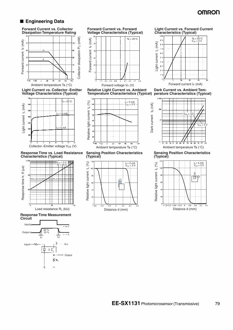
■ Engineering Data
Forward Current vs. Collector Dissipation Temperature Rating
Forward Current vs. Forward Voltage Characteristics (Typical)
Light Current vs. Forward Current Characteristics (Typical)
Light Current vs. Collector−Emitter Voltage Characteristics (Typical)
Relative Light Current vs. Ambient Temperature Characteristics (Typical)
Response Time vs. Load Resistance Characteristics (Typical)
Input
Output
Input
Output
90 %10 %
Sensing Position Characteristics (Typical)
Response Time Measurement Circuit
Sensing Position Characteristics (Typical)
Distance d (mm) Distance d (mm)
VCE = 2 V
VCE = 10 V
Ambient temperature Ta (°C)
Col
lect
or d
issi
patio
n P
C (
mW
)
Forward voltage VF (V)
For
war
d cu
rren
t I F
(m
A)
For
war
d cu
rren
t I F
(m
A)
Forward current IF (mA)
Ligh
t cur
rent
IL
(mA
)
Collector−Emitter voltage VCE (V)
Ligh
t cur
rent
IL
(mA
)
Ambient temperature Ta (°C)
Load resistance RL (kΩ)
Ta = 25°CVCE = 5 V
IF = 10 mA
IF = 5 mA
Ta = 25°C IF = 5 mA VCE = 5 V
IF = 5 mA VCE = 5 V Ta = 25°C
Res
pons
e tim
e tr,
tf (
μs)
Rel
ativ
e lig
ht c
urre
nt I
L (%
)
Dar
k cu
rren
t I D
(nA
)
Rel
ativ
e lig
ht c
urre
nt I
L (%
)
Ambient temperature Ta (°C)
Rel
ativ
e lig
ht c
urre
nt I
L (%
) IF = 5 mA VCE = 5 V
Ta = 25°C
Dark Current vs. Ambient Tem-perature Characteristics (Typical)
VCC = 5 V
EE-SX1131 Photomicrosensor (Transmissive) 79

Unit: mm (inch)
■ Tape and Reel
Reel
Tape
Tape configuration
Tape quantity2,000 pcs./reel
21±0.8 dia.2±0.513±0.5 dia.
80±1 dia.
330±2 dia.
12.4+20
18.4 max.
Product name
Quantity
Lot number
1.5 dia.
Terminating part (40 mm min.)
Pull-out directionEmpty
(40 mm min.)
Parts mounted Leading part (400 mm min.)
80 EE-SX1131 Photomicrosensor (Transmissive)

Precautions
■ Soldering Information
Reflow soldering• The following soldering paste is recommended:
Melting temperature: 216 to 220°CComposition: Sn 3.5 Ag 0.75 Cu
• The recommended thickness of the metal mask for screen printing is between 0.2 and 0.25 mm.• Set the reflow oven so that the temperature profile shown in the following chart is obtained for the upper surface of the product being soldered.
Manual soldering• Use ”Sn 60” (60% tin and 40% lead) or solder with silver content.• Use a soldering iron of less than 25 W, and keep the temperature of the iron tip at 300°C or below.• Solder each point for a maximum of three seconds.• After soldering, allow the product to return to room temperature before handling it.
StorageTo protect the product from the effects of humidity until the package is opened, dry-box storage is recommended. If this is not possible, store the product under the following conditions:
Temperature: 10 to 30°CHumidity: 60% max.
The product is packed in a humidity-proof envelope. Reflow soldering must be done within 48 hours after opening the envelope, during which time the product must be stored under 30°C at 80% maximum humidity.If it is necessary to store the product after opening the envelope, use dry-box storage or reseal the envelope.
BakingIf a product has remained packed in a humidity-proof envelope for six months or more, or if more than 48 hours have lapsed since the envelope was opened, bake the product under the following conditions before use:
Reel: 60°C for 24 hours or moreBulk: 80°C for 4 hours or more
260°C max.
Time
120 sec
Tem
pera
ture
1 to 5°C/s 150 to 180°C
40 sec max.
10 sec max.
1 to 5°C/s 255°C max.
230°C max.
EE-SX1131 Photomicrosensor (Transmissive) 81

Photomicrosensor (Transmissive)
EE-SX1137Be sure to read Precautions on page 25.
■ DimensionsNote: All units are in millimeters unless otherwise indicated.
■ Features• General-purpose model with a 5-mm-wide slot.• PCB mounting type.• High resolution with a 0.5-mm-wide aperture.
■ Absolute Maximum Ratings (Ta = 25°C)
Note: 1. Refer to the temperature rating chart if the ambient temper-ature exceeds 25°C.
2. The pulse width is 10 μs maximum with a frequency of100 Hz.
3. Complete soldering within 10 seconds.
■ Electrical and Optical Characteristics (Ta = 25°C)
Internal Circuit
K
A
C
E
Terminal No. Name
A Anode
K Cathode
C CollectorE Emitter
Dimensions Tolerance
3 mm max. ±0.3
3 < mm ≤ 6 ±0.375
6 < mm ≤ 10 ±0.45
10 < mm ≤ 18 ±0.55
18 < mm ≤ 30 ±0.65
Unless otherwise specified, the tolerances are as shown below.
Item Symbol Rated value
Emitter Forward current IF 50 mA (see note 1)
Pulse forward cur-rent
IFP 1 A (see note 2)
Reverse voltage VR 4 V
Detector Collector–Emitter voltage
VCEO 30 V
Emitter–Collector voltage
VECO ---
Collector current IC 20 mA
Collector dissipa-tion
PC 100 mW (see note 1)
Ambient tem-perature
Operating Topr –25°C to 85°CStorage Tstg –30°C to
100°CSoldering temperature Tsol 260°C
(see note 3)
Item Symbol Value Condition
Emitter Forward voltage VF 1.2 V typ., 1.5 V max. IF = 30 mA
Reverse current IR 0.01 μA typ., 10 μA max. VR = 4 V
Peak emission wavelength λP 940 nm typ. IF = 20 mA
Detector Light current IL 0.5 mA min., 14 mA max. IF = 20 mA, VCE = 10 V
Dark current ID 2 nA typ., 200 nA max. VCE = 10 V, 0 lx
Leakage current ILEAK --- ---
Collector–Emitter saturated volt-age
VCE (sat) 0.1 V typ., 0.4 V max. IF = 20 mA, IL = 0.1 mA
Peak spectral sensitivity wave-length
λP 850 nm typ. VCE = 10 V
Rising time tr 4 μs typ. VCC = 5 V, RL = 100 Ω, IL = 5 mA
Falling time tf 4 μs typ. VCC = 5 V, RL = 100 Ω, IL = 5 mA
82 EE-SX1137 Photomicrosensor (Transmissive)

■ Engineering Data
Forward Current vs. Collector Dissipation Temperature Rating
Forward Current vs. Forward Voltage Characteristics (Typical)
Light Current vs. Forward Current Characteristics (Typical)
Light Current vs. Collector−Emitter Voltage Characteristics (Typical)
Dark Current vs. Ambient Temperature Characteristics (Typical)
Distance d (mm)
Input
Output
Input
Output
90 %10 %
(Center of optical axis)
Sensing Position Characteristics (Typical)
Response Time Measurement Circuit
Ambient temperature Ta (°C)
Col
lect
or d
issi
patio
n P
C (
mW
)
Forward voltage VF (V)
For
war
d cu
rren
t I F
(m
A)
For
war
d cu
rren
t I F
(m
A)
Forward current IF (mA)
Ligh
t cur
rent
IL
(mA
)
Collector−Emitter voltage VCE (V)
Ligh
t cur
rent
IL
(mA
)
Ambient temperature Ta (°C)
Load resistance RL (kΩ)
Ta = −30°C
Ta = 25°C
Ta = 70°C
Ta = 25°CVCE = 10 V
IF = 40 mA
IF = 30 mA
IF = 20 mA
IF = 10 mA
Ta = 25°C VCE = 10 V0 lx
IF = 20 mA VCE = 5 V
IF = 20 mA VCE = 10 V Ta = 25°C
VCC = 5 V Ta = 25°C
Res
pons
e tim
e tr,
tf (
μs)
Rel
ativ
e lig
ht c
urre
nt I
L (%
)
Dar
k cu
rren
t I D
(nA
)
Rel
ativ
e lig
ht c
urre
nt I
L (%
)
IF = 50 mA
Ambient temperature Ta (°C)
Relative Light Current vs. Ambi-ent Temperature Characteristics (Typical)
Response Time vs. Load Resist-ance Characteristics (Typical)
Distance d (mm)
Sensing Position Characteristics (Typical)
Rel
ativ
e lig
ht c
urre
nt I
L (%
) 100
80
60
40
20
0−1.5−2.0 −1.0 −0.5 0 0.5 1.0 1.5 2.0
120
d
IF = 20 mA VCE = 10 V Ta = 25°C
(Cen
ter
of o
ptic
al a
xis)
EE-SX1137 Photomicrosensor (Transmissive) 83

Photomicrosensor (Transmissive)
EE-SX1140Be sure to read Precautions on page 25.
■ DimensionsNote: All units are in millimeters unless otherwise indicated.
■ Features• General-purpose model with a 14-mm-wide slot.• 16.3-mm-tall model with a deep slot.• PCB mounting type.
■ Absolute Maximum Ratings (Ta = 25°C)
Note: 1. Refer to the temperature rating chart if the ambient temper-ature exceeds 25°C.
2. The pulse width is 10 μs maximum with a frequency of100 Hz.
3. Complete soldering within 10 seconds.
■ Electrical and Optical Characteristics (Ta = 25°C)
Internal Circuit
K
A
C
E
Terminal No. Name
A Anode
K CathodeC Collector
E Emitter
Dimensions Tolerance
3 mm max. ±0.3
3 < mm ≤ 6 ±0.375
6 < mm ≤ 10 ±0.45
10 < mm ≤ 18 ±0.55
18 < mm ≤ 30 ±0.65
Cross section AA
Unless otherwise specified, the tolerances are as shown below.
Four, C0.3Four, 0.8
Four, 0.8
14
3.2±0.1 dia. through-hole
23
3 5
CE
12.5±0.15
Four, 0.5
Four, 0.25
(19.9)
BA
BA
1.5
(2.5)
0.2
16.3
5.2
2.8
Optical axis
(13.5)
4.5±0.5K A
1.5
(2.5)
Cross section BB
Item Symbol Rated value
Emitter Forward current IF 50 mA (see note 1)
Pulse forward cur-rent
IFP 1 A (see note 2)
Reverse voltage VR 4 V
Detector Collector–Emitter voltage
VCEO 30 V
Emitter–Collector voltage
VECO ---
Collector current IC 20 mA
Collector dissipa-tion
PC 100 mW (see note 1)
Ambient tem-perature
Operating Topr –25°C to 85°CStorage Tstg –30°C to
100°CSoldering temperature Tsol 260°C
(see note 3)
Item Symbol Value Condition
Emitter Forward voltage VF 1.2 V typ., 1.5 V max. IF = 30 mA
Reverse current IR 0.01 μA typ., 10 μA max. VR = 4 V
Peak emission wavelength λP 940 nm typ. IF = 20 mA
Detector Light current IL 0.4 mA min. IF = 20 mA, VCE = 10 V
Dark current ID 2 nA typ., 200 nA max. VCE = 10 V, 0 lx
Leakage current ILEAK --- ---
Collector–Emitter saturated volt-age
VCE (sat) 0.1 V typ., 0.4 V max. IF = 20 mA, IL = 0.1 mA
Peak spectral sensitivity wave-length
λP 850 nm typ. VCE = 10 V
Rising time tr 4 μs typ. VCC = 5 V, RL = 100 Ω, IL = 5 mA
Falling time tf 4 μs typ. VCC = 5 V, RL = 100 Ω, IL = 5 mA
84 EE-SX1140 Photomicrosensor (Transmissive)

■ Engineering Data
0
10
8
6
4
2
010 20 30 40 50
Forward Current vs. Collector Dissipation Temperature Rating
Forward Current vs. Forward Voltage Characteristics (Typical)
Light Current vs. Forward Current Characteristics (Typical)
Light Current vs. Collector−Emitter Voltage Characteristics (Typical)
Dark Current vs. Ambient Temperature Characteristics (Typical)
Distance d (mm)
Sensing Position Characteristics (Typical)
Response Time Measurement Circuit
Ambient temperature Ta (°C)
Col
lect
or d
issi
patio
n P
C (
mW
)
Forward voltage VF (V)
For
war
d cu
rren
t I F
(m
A)
For
war
d cu
rren
t I F
(m
A)
Forward current IF (mA)
Ligh
t cur
rent
IL
(mA
)Collector−Emitter voltage VCE (V)
Ligh
t cur
rent
IL
(mA
)
Ambient temperature Ta (°C)
Load resistance RL (kΩ)
Ta = −30°C
Ta = 25°C
Ta = 70°C
Ta = 25°CVCE = 10 V
IF = 40 mA
IF = 30 mA
IF = 20 mA
IF = 10 mA
Ta = 25°C VCE = 10 V0 lxIF = 20 mA
VCE = 5 V
IF = 20 mA VCE = 10 V Ta = 25°C
VCC = 5 V Ta = 25°C
Res
pons
e tim
e tr,
tf (
μs)
Rel
ativ
e lig
ht c
urre
nt I
L (%
)
Dar
k cu
rren
t I D
(nA
)
Rel
ativ
e lig
ht c
urre
nt I
L (%
)
IF = 50 mA
Ambient temperature Ta (°C)
60
50
40
30
20
10
0−40 −20 0 20 40 60 80 100
150
100
50
0
PC
IF
60
50
40
30
20
10
00 0.2 0.4 0.6 0.8 1 1.2 1.4 1.6 1.8
0 1 2 3 4 5 6 7 8 9 10
10
9
8
7
6
5
4
3
2
1
120
110
100
90
80
70
60−40 −20 0 20 40 60 80 100
10,000
1,000
100
10
1
0.1
0.01
0.001−30 −20 −10 0 10 20 30 40 50 60 70 80 90
10,000
0.01
tr
tf
0.1 101
1,000
100
10
1
100
80
60
40
20
0−1.5 −0.75 0 0.75 1.5 2.25 3
d
120
(Center of optical axis)
90%10%
tt ft r
t0
Input
Output
VCC
RL
Input
0
Output
IL
Relative Light Current vs. Ambi-ent Temperature Characteristics (Typical)
Response Time vs. Load Resist-ance Characteristics (Typical)
Distance d (mm)
Sensing Position Characteristics (Typical)
Rel
ativ
e lig
ht c
urre
nt I
L (%
) 100
80
60
40
20
0−1.5−2.0 −1.0 −0.5 0 0.5 1.0 1.5 2.0
120
d
IF = 20 mA VCE = 10 V Ta = 25°C
(Cen
ter
of o
ptic
al a
xis)
EE-SX1140 Photomicrosensor (Transmissive) 85

Photomicrosensor (Transmissive)
EE-SX1235A-P2Be sure to read Precautions on page 25.
■ DimensionsNote: All units are in millimeters unless otherwise indicated.
■ Features• Snap-in mounting model.• Mounts to 1.0-, 1.2- and 1.6-mm-thick PCBs.• High resolution with a 0.5-mm-wide aperture.• 5-mm-wide slot.• Connects to Tyco Electronics AMP’s CT-series connectors.
■ Absolute Maximum Ratings (Ta = 25°C)
Note: Refer to the temperature rating chart if the ambient tempera-ture exceeds 25°C.
■ Electrical and Optical Characteristics (Ta = 25°C)
Internal Circuit
Terminal No. Name
A Anode
C Collector
K, E Cathode, Emitter
Dimensions Tolerance
3 mm max. ±0.3
3 < mm ≤ 6 ±0.375
6 < mm ≤ 10 ±0.45
10 < mm ≤ 18 ±0.55
18 < mm ≤ 30 ±0.65
Note: The asterisked dimension is specified by datum A only.
Recommended Mating Connectors:Tyco Electronics AMP 173977-3 (press-fit connector)
175778-3 (crimp connector) 179228-3 (crimp connector)
3.2
(Ape
rtur
e w
idth
)
0.5 (Aperture width)
Post header 292250-3(Tyco Electronics AMP)
Four, R0.5
(see note)
(3) A (2) K, E (1) C
Unless otherwise specified, the tolerances are as shown below.
−0.3
−0.1
+1
+0.15
+0.1−0.2+0.1−0.2+0.1−0.2
−0.15
−0.2
+0.1
+0.1
+0.1−0.2
−0.0
5
A
+0.
1 3
±0.2
(10.
1)Optical axis
(5.8
)
7.6
0.7
4
6
17
5 5 5
1.1
5.612
.63.
3
(1.2
)(4
.6)
(10)
3.55.87.3
±0.2
5.87.3
0.8
8
8.5 (11)6
8.9
7.6
+0
.1−0
.05
+0
.1−0
.05
+0
.15
−0.0
5
1.1
1.3
1.7
A
Item Symbol Rated value
Emitter Forward current IF 50 mA (see note)
Pulse forward cur-rent
IFP ---
Reverse voltage VR 4 V
Detector Collector–Emitter voltage
VCEO 30 V
Emitter–Collector voltage
VECO 5 V
Collector current IC 20 mA
Collector dissipa-tion
PC 100 mW (see note)
Ambient tem-perature
Operating Topr –25°C to 95°CStorage Tstg –40°C to 100°C
Soldering temperature Tsol ---
Item Symbol Value Condition
Emitter Forward voltage VF 1.2 V typ., 1.5 V max. IF = 30 mA
Reverse current IR 0.01 μA typ., 10 μA max. VR = 4 V
Peak emission wavelength λP 940 nm typ. IF = 30 mA
Detector Light current IL 0.6 mA min., 14 mA max. IF = 20 mA, VCE = 5 V
Dark current ID 200 nA max. VCE = 10 V, 0 lx
Leakage current ILEAK --- ---
Collector–Emitter saturated volt-age
VCE (sat) 0.1 V typ., 0.4 V max. IF = 20 mA, IL = 0.3 mA
Peak spectral sensitivity wave-length
λP 850 nm typ. VCE = 5 V
Rising time tr 8 μs typ. VCC = 5 V, RL = 100 Ω, IL = 1 mA
Falling time tf 8 μs typ. VCC = 5 V, RL = 100 Ω, IL = 1 mA
86 EE-SX1235A-P2 Photomicrosensor (Transmissive)

■ Engineering Data
Refer to EE-SX4235A-P2 on page 140.
Forward Current vs. Collector Dissipation Temperature Rating
Forward Current vs. Forward Voltage Characteristics (Typical)
Light Current vs. Forward Current Characteristics (Typical)
Light Current vs. Collector−Emitter Voltage Characteristics (Typical)
Dark Current vs. Ambient Temperature Characteristics (Typical)
Distance d (mm)
(Center of optical axis)
Output
Input
Output
Input
VCC
GND
10%90%
Sensing Position Characteristics (Typical)
Response Time Measurement Circuit
Ambient temperature Ta (°C)
Col
lect
or d
issi
patio
n P
C (
mW
)
Forward voltage VF (V)
For
war
d cu
rren
t I F
(m
A)
For
war
d cu
rren
t I F
(m
A)
Forward current IF (mA)
Ligh
t cur
rent
IL
(mA
)Collector−Emitter voltage VCE (V)
Ligh
t cur
rent
IL
(mA
)
Ambient temperature Ta (°C)
Load resistance RL (kΩ)
Ta = −30°C
Ta = 25°C
Ta = 70°C
Ta = 25°CVCE = 10 V
IF = 40 mA
IF = 30 mA
IF = 20 mA
IF = 10 mA
Ta = 25°C VCE = 10 V0 lx
IF = 20 mA VCE = 5 V
IF = 20 mA VCE = 10 V Ta = 25°C
VCC = 5 V Ta = 25°C
Res
pons
e tim
e tr,
tf (
μs)
Rel
ativ
e lig
ht c
urre
nt I
L (%
)
Dar
k cu
rren
t I D
(nA
)
Rel
ativ
e lig
ht c
urre
nt I
L (%
)
IF = 50 mA
Ambient temperature Ta (°C)
IF
PC
Relative Light Current vs. Ambi-ent Temperature Characteristics (Typical)
Response Time vs. Load Resist-ance Characteristics (Typical)
Distance d (mm)
Sensing Position Characteristics (Typical)
Rel
ativ
e lig
ht c
urre
nt I
L (%
) 100
80
60
40
20
0−1.5−2.0 −1.0 −0.5 0 0.5 1.0 1.5 2.0
120
d
IF = 20 mA VCE = 10 V Ta = 25°C
(Cen
ter
of o
ptic
al a
xis)
EE-SX1235A-P2 Photomicrosensor (Transmissive) 87

Photomicrosensor (Transmissive)
EE-SX129Be sure to read Precautions on page 25.
■ DimensionsNote: All units are in millimeters unless otherwise indicated.
■ Features• High-resolution model with a 0.2-mm-wide sensing aperture.• PCB mounting type.
■ Absolute Maximum Ratings (Ta = 25°C)
Note: 1. Refer to the temperature rating chart if the ambient temper-ature exceeds 25°C.
2. The pulse width is 10 μs maximum with a frequency of100 Hz.
3. Complete soldering within 10 seconds.
■ Electrical and Optical Characteristics (Ta = 25°C)
Internal Circuit
Terminal No. Name
A Anode
K CathodeC Collector
E Emitter
Dimensions Tolerance
3 mm max. ±0.3
3 < mm ≤ 6 ±0.375
6 < mm ≤ 10 ±0.45
10 < mm ≤ 18 ±0.55
18 < mm ≤ 30 ±0.65
2.1+0.20 dia. holes
Cross section AA
Optical axis
Part B
0.5 min.
A
K
E
C
Unless otherwise specified, the tolerances are as shown below.
138
5
6
3
0.25
A
A
13.4±2
2
58
0.2
3±0.3
B
1+0.50
E
C
A
K
EC
AK
0.5
0.8
1.94±0.2
0.2
2
2.5
2.5
R2.55
9.2±0.3
Item Symbol Rated value
Emitter Forward current IF 50 mA (see note 1)
Pulse forward cur-rent
IFP 1 A (see note 2)
Reverse voltage VR 4 V
Detector Collector–Emitter voltage
VCEO 30 V
Emitter–Collector voltage
VECO ---
Collector current IC 20 mA
Collector dissipa-tion
PC 100 mW (see note 1)
Ambient tem-perature
Operating Topr –25°C to 85°CStorage Tstg –40°C to
100°CSoldering temperature Tsol 260°C
(see note 3)
Item Symbol Value Condition
Emitter Forward voltage VF 1.2 V typ., 1.5 V max. IF = 30 mA
Reverse current IR 0.01 μA typ., 10 μA max. VR = 4 V
Peak emission wavelength λP 920 nm typ. IF = 20 mA
Detector Light current IL 0.2 mA min. IF = 20 mA, VCE = 10 V
Dark current ID 2 nA typ., 200 nA max. VCE = 10 V, 0 lx
Leakage current ILEAK --- ---
Collector–Emitter saturated volt-age
VCE (sat) --- ---
Peak spectral sensitivity wave-length
λP 850 nm typ. VCE = 10 V
Rising time tr 4 μs typ. VCC = 5 V, RL = 100 Ω, IL = 5 mA
Falling time tf 4 μs typ. VCC = 5 V, RL = 100 Ω, IL = 5 mA
88 EE-SX129 Photomicrosensor (Transmissive)

■ Engineering Data
Forward Current vs. Collector Dissipation Temperature Rating
Forward Current vs. Forward Voltage Characteristics (Typical)
Light Current vs. Forward Current Characteristics (Typical)
Light Current vs. Collector−Emitter Voltage Characteristics (Typical)
Dark Current vs. Ambient Temperature Characteristics (Typical)
Distance d (mm)
Input
Output
Input
Output
90 %10 %
Vcc
(Center of optical axis)
0-0.1-0.2 0.1 0.2 0.3 0.4
Sensing Position Characteristics (Typical)
Response Time Measurement Circuit
Ambient temperature Ta (°C)
Col
lect
or d
issi
patio
n P
C (
mW
)
Forward voltage VF (V)
For
war
d cu
rren
t I F
(m
A)
For
war
d cu
rren
t I F
(m
A)
Forward current IF (mA)
Ligh
t cur
rent
IL
(mA
)
Collector−Emitter voltage VCE (V)
Ligh
t cur
rent
IL
(mA
)
Ambient temperature Ta (°C)
Load resistance RL (kΩ)
Ta = −30°C
Ta = 25°C
Ta = 70°C
Ta = 25°CVCE = 10 V
IF = 40 mA
IF = 30 mA
IF = 20 mA
IF = 10 mA
Ta = 25°C VCE = 10 V0 lx
IF = 20 mA VCE = 5 V
IF = 20 mA VCE = 10 V Ta = 25°C
VCC = 5 V Ta = 25°C
Res
pons
e tim
e tr,
tf (
μs)
Rel
ativ
e lig
ht c
urre
nt I
L (%
)
Dar
k cu
rren
t I D
(nA
)
Rel
ativ
e lig
ht c
urre
nt I
L (%
)
IF = 50 mA
Ambient temperature Ta (°C)
IF
PC
Relative Light Current vs. Ambi-ent Temperature Characteristics (Typical)
Response Time vs. Load Resist-ance Characteristics (Typical)
Distance d (mm)
Sensing Position Characteristics (Typical)
Rel
ativ
e lig
ht c
urre
nt I
L (%
) 100
80
60
40
20
0−1.5−2.0 −1.0 −0.5 0 0.5 1.0 1.5 2.0
120
d
IF = 20 mA VCE = 10 V Ta = 25°C
(Cen
ter
of o
ptic
al a
xis)
EE-SX129 Photomicrosensor (Transmissive) 89

Photomicrosensor (Transmissive)
EE-SX138Be sure to read Precautions on page 25.
■ DimensionsNote: All units are in millimeters unless otherwise indicated.
■ Features• General-purpose model with a 3.4-mm-wide slot.• PCB mounting type.• High resolution with a 0.5-mm-wide aperture.• Screw-mounting possible.
■ Absolute Maximum Ratings (Ta = 25°C)
Note: 1. Refer to the temperature rating chart if the ambient temper-ature exceeds 25°C.
2. The pulse width is 10 μs maximum with a frequency of100 Hz.
3. Complete soldering within 10 seconds.
■ Electrical and Optical Characteristics (Ta = 25°C)
Internal Circuit
Terminal No. Name
A Anode
K Cathode
C Collector
E Emitter
Dimensions Tolerance
3 mm max. ±0.2
3 < mm ≤ 6 ±0.24
6 < mm ≤ 10 ±0.29
10 < mm ≤ 18 ±0.35
18 < mm ≤ 30 ±0.42
Four, R1.25
Four, 0.5
Four, 1 R
Four, 0.25
Four, 0.1 taper
2.1 × 0.5 Aperture
Part A
2.54±0.27.6±0.3
23.8
0.24.75
14.313.6
A
K
E
C
(Optical axis)
Unless otherwise specified, the tolerances are as shown below.
Item Symbol Rated value
Emitter Forward current IF 50 mA (see note 1)
Pulse forward cur-rent
IFP 1 A (see note 2)
Reverse voltage VR 4 V
Detector Collector–Emitter voltage
VCEO 30 V
Emitter–Collector voltage
VECO ---
Collector current IC 20 mA
Collector dissipa-tion
PC 100 mW (see note 1)
Ambient tem-perature
Operating Topr –25°C to 85°CStorage Tstg –40°C to
100°CSoldering temperature Tsol 260°C
(see note 3)
Item Symbol Value Condition
Emitter Forward voltage VF 1.2 V typ., 1.5 V max. IF = 30 mA
Reverse current IR 0.01 μA typ., 10 μA max. VR = 4 V
Peak emission wavelength λP 940 nm typ. IF = 20 mA
Detector Light current IL 1.9 mA min., 14 mA max. IF = 20 mA, VCE = 10 V
Dark current ID 2 nA typ., 200 nA max. VCE = 10 V, 0 lx
Leakage current ILEAK --- ---
Collector–Emitter saturated volt-age
VCE (sat) 0.1 V typ., 0.4 V max. IF = 20 mA, IL = 0.1 mA
Peak spectral sensitivity wave-length
λP 850 nm typ. VCE = 10 V
Rising time tr 4 μs typ. VCC = 5 V, RL = 100 Ω, IL = 5 mA
Falling time tf 4 μs typ. VCC = 5 V, RL = 100 Ω, IL = 5 mA
90 EE-SX138 Photomicrosensor (Transmissive)
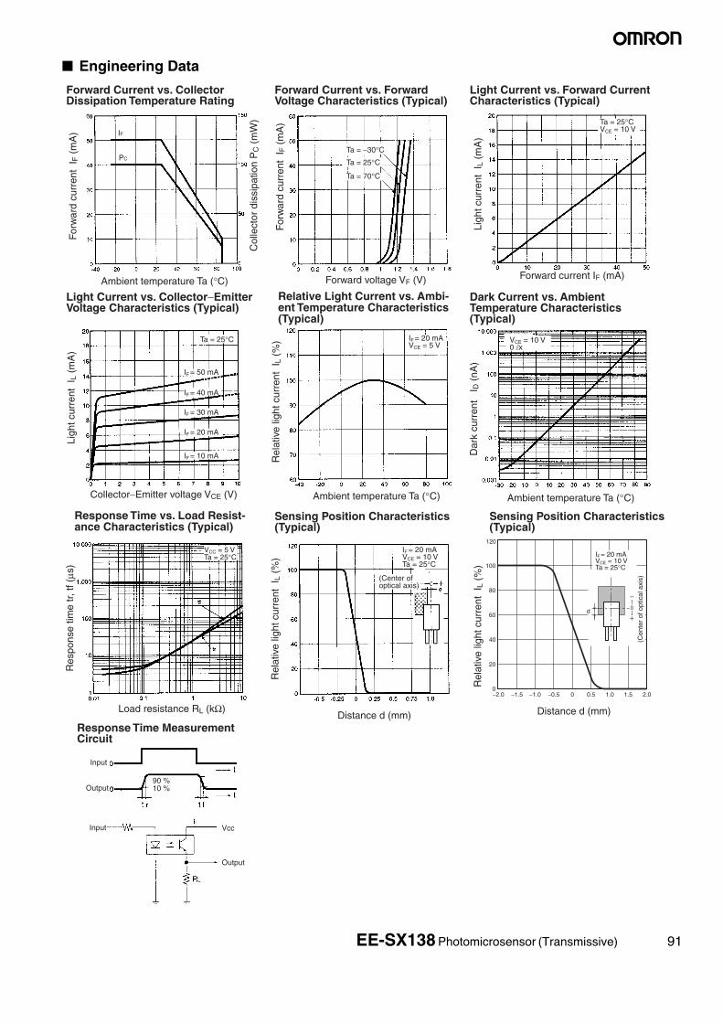
■ Engineering Data
Forward Current vs. Collector Dissipation Temperature Rating
Forward Current vs. Forward Voltage Characteristics (Typical)
Light Current vs. Forward Current Characteristics (Typical)
Light Current vs. Collector−Emitter Voltage Characteristics (Typical)
Dark Current vs. Ambient Temperature Characteristics (Typical)
Distance d (mm)
Input
Output
Input
Output
90 %10 %
Vcc
(Center of optical axis)
Sensing Position Characteristics (Typical)
Response Time Measurement Circuit
Ambient temperature Ta (°C)
Col
lect
or d
issi
patio
n P
C (
mW
)
Forward voltage VF (V)
For
war
d cu
rren
t I F
(m
A)
For
war
d cu
rren
t I F
(m
A)
Forward current IF (mA)
Ligh
t cur
rent
IL
(mA
)
Collector−Emitter voltage VCE (V)
Ligh
t cur
rent
IL
(mA
)
Ambient temperature Ta (°C)
Load resistance RL (kΩ)
Ta = −30°C
Ta = 25°C
Ta = 70°C
Ta = 25°CVCE = 10 V
IF = 40 mA
IF = 30 mA
IF = 20 mA
IF = 10 mA
Ta = 25°C VCE = 10 V0 lx
IF = 20 mA VCE = 5 V
IF = 20 mA VCE = 10 V Ta = 25°C
VCC = 5 V Ta = 25°C
Res
pons
e tim
e tr,
tf (
μs)
Rel
ativ
e lig
ht c
urre
nt I
L (%
)
Dar
k cu
rren
t I D
(nA
)
Rel
ativ
e lig
ht c
urre
nt I
L (%
)
IF = 50 mA
Ambient temperature Ta (°C)
IF
PC
Relative Light Current vs. Ambi-ent Temperature Characteristics (Typical)
Response Time vs. Load Resist-ance Characteristics (Typical)
Distance d (mm)
Sensing Position Characteristics (Typical)
Rel
ativ
e lig
ht c
urre
nt I
L (%
) 100
80
60
40
20
0−1.5−2.0 −1.0 −0.5 0 0.5 1.0 1.5 2.0
120
d
IF = 20 mA VCE = 10 V Ta = 25°C
(Cen
ter
of o
ptic
al a
xis)
EE-SX138 Photomicrosensor (Transmissive) 91

Photomicrosensor (Transmissive)
EE-SX153Be sure to read Precautions on page 25.
■ DimensionsNote: All units are in millimeters unless otherwise indicated.
■ Features• General-purpose model with a 3.4-mm-wide slot.• PCB mounting type.• High resolution with a 0.5-mm-wide aperture.• With a horizontal sensing aperture.• Screw-mounting possible.
■ Absolute Maximum Ratings (Ta = 25°C)
Note: 1. Refer to the temperature rating chart if the ambient temper-ature exceeds 25°C.
2. The pulse width is 10 μs maximum with a frequency of100 Hz.
3. Complete soldering within 10 seconds.
■ Electrical and Optical Characteristics (Ta = 25°C)
Internal Circuit
K
A
C
E
Terminal No. Name
A Anode
K CathodeC Collector
E Emitter
Dimensions Tolerance
3 mm max. ±0.3
3 < mm ≤ 6 ±0.375
6 < mm ≤ 10 ±0.45
10 < mm ≤ 18 ±0.55
18 < mm ≤ 30 ±0.65
3.2±0.2dia. holes
Four, 0.25Four, 0.8Four, 1.5
Two, R1
Cross section AA
Two, 2.54
Unless otherwise specified, the tolerances are as shown below.
6.2
13.6
0.3
6.4
0.5
2
3.4±0.2
A 3.2
36
3
10.2
0.2
A
7.6±0.2
K
K
A
A
C
C
E
E
2.1
0.5
1.20.6
7.2±0.2
7.8
JAP
AN
EE
-SX
153
Item Symbol Rated value
Emitter Forward current IF 50 mA (see note 1)
Pulse forward cur-rent
IFP 1 A (see note 2)
Reverse voltage VR 4 V
Detector Collector–Emitter voltage
VCEO 30 V
Emitter–Collector voltage
VECO ---
Collector current IC 20 mA
Collector dissipa-tion
PC 100 mW (see note 1)
Ambient tem-perature
Operating Topr –25°C to 85°CStorage Tstg –40°C to
100°CSoldering temperature Tsol 260°C
(see note 3)
Item Symbol Value Condition
Emitter Forward voltage VF 1.2 V typ., 1.5 V max. IF = 30 mA
Reverse current IR 0.01 μA typ., 10 μA max. VR = 4 V
Peak emission wavelength λP 940 nm typ. IF = 20 mA
Detector Light current IL 0.5 mA min., 14 mA max. IF = 20 mA, VCE = 10 V
Dark current ID 2 nA typ., 200 nA max. VCE = 10 V, 0 lx
Leakage current ILEAK --- ---
Collector–Emitter saturated volt-age
VCE (sat) 0.1 V typ., 0.4 V max. IF = 20 mA, IL = 0.1 mA
Peak spectral sensitivity wave-length
λP 850 nm typ. VCE = 10 V
Rising time tr 4 μs typ. VCC = 5 V, RL = 100 Ω, IL = 5 mA
Falling time tf 4 μs typ. VCC = 5 V, RL = 100 Ω, IL = 5 mA
92 EE-SX153 Photomicrosensor (Transmissive)
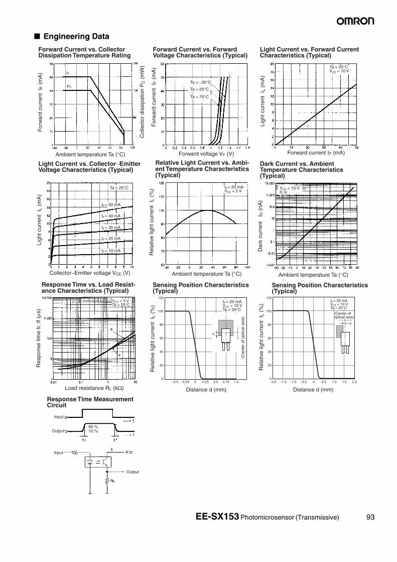
■ Engineering Data
Forward Current vs. Collector Dissipation Temperature Rating
Forward Current vs. Forward Voltage Characteristics (Typical)
Light Current vs. Forward Current Characteristics (Typical)
Light Current vs. Collector−Emitter Voltage Characteristics (Typical)
Dark Current vs. Ambient Temperature Characteristics (Typical)
Distance d (mm)
Input
Output
Input
Output
90 %10 %
(Cen
ter
of o
ptic
al a
xis)
Sensing Position Characteristics (Typical)
Response Time Measurement Circuit
Ambient temperature Ta (°C)
Col
lect
or d
issi
patio
n P
C (
mW
)
Forward voltage VF (V)
For
war
d cu
rren
t I F
(m
A)
For
war
d cu
rren
t I F
(m
A)
Forward current IF (mA)
Ligh
t cur
rent
IL
(mA
)
Collector−Emitter voltage VCE (V)
Ligh
t cur
rent
IL
(mA
)
Ambient temperature Ta (°C)
Load resistance RL (kΩ)
Ta = −30°C
Ta = 25°C
Ta = 70°C
Ta = 25°CVCE = 10 V
IF = 40 mA
IF = 30 mA
IF = 20 mA
IF = 10 mA
Ta = 25°C VCE = 10 V0 lx
IF = 20 mA VCE = 5 V
IF = 20 mA VCE = 10 V Ta = 25°C
VCC = 5 V Ta = 25°C
Res
pons
e tim
e tr,
tf (
μs)
Rel
ativ
e lig
ht c
urre
nt I
L (%
)
Dar
k cu
rren
t I D
(nA
)
Rel
ativ
e lig
ht c
urre
nt I
L (%
)
IF = 50 mA
Ambient temperature Ta (°C)
IF
PC
Relative Light Current vs. Ambi-ent Temperature Characteristics (Typical)
Response Time vs. Load Resist-ance Characteristics (Typical)
100
80
60
40
20
0−1.5−2.0 −1.0 −0.5 0 0.5 1.0 1.5 2.0
120
d
Distance d (mm)
(Center of optical axis)
Sensing Position Characteristics (Typical)
IF = 20 mA VCE = 10 V Ta = 25°C
Rel
ativ
e lig
ht c
urre
nt I
L (%
)
d
100
80
60
40
20
0−0.5 −0.25 0 0.25 0.5 0.75 1.0
120
EE-SX153 Photomicrosensor (Transmissive) 93

Photomicrosensor (Transmissive)
EE-SX198Be sure to read Precautions on page 25.
■ DimensionsNote: All units are in millimeters unless otherwise indicated.
■ Features• General-purpose model with a 3-mm-wide slot.• PCB mounting type.• High resolution with a 0.5-mm-wide aperture.
■ Absolute Maximum Ratings (Ta = 25°C)
Note: 1. Refer to the temperature rating chart if the ambient temper-ature exceeds 25°C.
2. The pulse width is 10 μs maximum with a frequency of100 Hz.
3. Complete soldering within 10 seconds.
■ Electrical and Optical Characteristics (Ta = 25°C)
Internal Circuit
K
A
C
E
Terminal No. Name
A Anode
K CathodeC CollectorE Emitter
Four, C0.3
Four, 0.5±0.1Four, 0.25±0.1
Two, C1±0.3
Optical axis
Cross section BBCross section AA
6.5+0.1
2.5±0.1
6.2±0.5
0.5±0.1
8.5±0.1
5±0.1
12.2±0.3
10±0.2
9.2±0.3
Unless otherwise specified, the tolerances are ±0.2 mm.
Item Symbol Rated value
Emitter Forward current IF 50 mA (see note 1)
Pulse forward cur-rent
IFP 1 A (see note 2)
Reverse voltage VR 4 V
Detector Collector–Emitter voltage
VCEO 30 V
Emitter–Collector voltage
VECO ---
Collector current IC 20 mA
Collector dissipa-tion
PC 100 mW (see note 1)
Ambient tem-perature
Operating Topr –25°C to 85°CStorage Tstg –30°C to
100°CSoldering temperature Tsol 260°C
(see note 3)
Item Symbol Value Condition
Emitter Forward voltage VF 1.2 V typ., 1.4 V max. IF = 30 mA
Reverse current IR 0.01 μA typ., 10 μA max. VR = 4 V
Peak emission wavelength λP 940 nm typ. IF = 20 mA
Detector Light current IL 0.5 mA min., 14 mA max. IF = 20 mA, VCE = 5 V
Dark current ID 2 nA typ., 200 nA max. VCE = 20 V, 0 lx
Leakage current ILEAK --- ---
Collector–Emitter saturated volt-age
VCE (sat) 0.1 V typ., 0.4 V max. IF = 40 mA, IL = 0.5 mA
Peak spectral sensitivity wave-length
λP 850 nm typ. VCE = 10 V
Rising time tr 4 μs typ. VCC = 5 V, RL = 100 Ω, IL = 5 mA
Falling time tf 4 μs typ. VCC = 5 V, RL = 100 Ω, IL = 5 mA
94 EE-SX198 Photomicrosensor (Transmissive)

■ Engineering Data
Forward Current vs. Collector Dissipation Temperature Rating
Forward Current vs. Forward Voltage Characteristics (Typical)
Light Current vs. Forward Current Characteristics (Typical)
Light Current vs. Collector−Emitter Voltage Characteristics (Typical)
Dark Current vs. Ambient Temperature Characteristics (Typical)
Distance d (mm)
Input
Output
Input
Output
90 %10 %
(Center of optical axis)
Sensing Position Characteristics (Typical)
Response Time Measurement Circuit
Ambient temperature Ta (°C)
Col
lect
or d
issi
patio
n P
C (
mW
)
Forward voltage VF (V)
For
war
d cu
rren
t I F
(m
A)
For
war
d cu
rren
t I F
(m
A)
Forward current IF (mA)
Ligh
t cur
rent
IL
(mA
)
Collector−Emitter voltage VCE (V)
Ligh
t cur
rent
IL
(mA
)
Ambient temperature Ta (°C)
Load resistance RL (kΩ)
Ta = −30°C
Ta = 25°C
Ta = 70°C
Ta = 25°CVCE = 10 V
IF = 40 mA
IF = 30 mA
IF = 20 mA
IF = 10 mA
Ta = 25°C VCE = 10 V0 lx
IF = 20 mA VCE = 5 V
IF = 20 mA VCE = 10 V Ta = 25°C
VCC = 5 V Ta = 25°C
Res
pons
e tim
e tr,
tf (
μs)
Rel
ativ
e lig
ht c
urre
nt I
L (%
)
Dar
k cu
rren
t I D
(nA
)
Rel
ativ
e lig
ht c
urre
nt I
L (%
)
IF = 50 mA
Ambient temperature Ta (°C)
IF
PC
Relative Light Current vs. Ambi-ent Temperature Characteristics (Typical)
Response Time vs. Load Resist-ance Characteristics (Typical)
Distance d (mm)
Sensing Position Characteristics (Typical)
Rel
ativ
e lig
ht c
urre
nt I
L (%
) 100
80
60
40
20
0−1.5−2.0 −1.0 −0.5 0 0.5 1.0 1.5 2.0
120
d
IF = 20 mA VCE = 10 V Ta = 25°C
(Cen
ter
of o
ptic
al a
xis)
EE-SX198 Photomicrosensor (Transmissive) 95

7Photomicrosensor (Transmissive)
EE-SX199Be sure to read Precautions on page 25.
■ DimensionsNote: All units are in millimeters unless otherwise indicated.
■ Features• General-purpose model with a 3-mm-wide slot.• PCB mounting type.• High resolution with a 0.5-mm-wide aperture.• With a positioning boss.
■ Absolute Maximum Ratings (Ta = 25°C)
Note: 1. Refer to the temperature rating chart if the ambient temper-ature exceeds 25°C.
2. The pulse width is 10 μs maximum with a frequency of100 Hz.
3. Complete soldering within 10 seconds.
■ Electrical and Optical Characteristics (Ta = 25°C)
Internal Circuit
K
A
C
E
Terminal No. NameA Anode
K CathodeC Collector
E Emitter
Four, 0.5±0.1Four, 0.25±0.1
Two, C1±0.3Four, C0.3
Two, 0.7 0-0.1 dia.
Optical axis
Cross section BB
Cross section AAC
E
K
A
6.5±0.1
6.2±0.5
10±0.2
12.2±0.3
9.2±0.3
8.5±0.1
0.5±0.1
5±0.1
2.5±0.1
4.3
Unless otherwise specified, the tolerances are ±0.2 mm.
Item Symbol Rated value
Emitter Forward current IF 50 mA (see note 1)
Pulse forward cur-rent
IFP 1 A (see note 2)
Reverse voltage VR 4 V
Detector Collector–Emitter voltage
VCEO 30 V
Emitter–Collector voltage
VECO ---
Collector current IC 20 mA
Collector dissipa-tion
PC 100 mW (see note 1)
Ambient tem-perature
Operating Topr –25°C to 85°CStorage Tstg –40°C to
100°CSoldering temperature Tsol 260°C
(see note 3)
Item Symbol Value Condition
Emitter Forward voltage VF 1.2 V typ., 1.4 V max. IF = 30 mA
Reverse current IR 0.01 μA typ., 10 μA max. VR = 4 V
Peak emission wavelength λP 940 nm typ. IF = 20 mA
Detector Light current IL 0.5 mA min., 14 mA max. IF = 20 mA, VCE = 5 V
Dark current ID 2 nA typ., 200 nA max. VCE = 20 V, 0 lx
Leakage current ILEAK --- ---
Collector–Emitter saturated volt-age
VCE (sat) 0.1 V typ., 0.4 V max. IF = 40 mA, IL = 0.5 mA
Peak spectral sensitivity wave-length
λP 850 nm typ. VCE = 10 V
Rising time tr 4 μs typ. VCC = 5 V, RL = 100 Ω, IL = 5 mA
Falling time tf 4 μs typ. VCC = 5 V, RL = 100 Ω, IL = 5 mA
96 EE-SX199 Photomicrosensor (Transmissive)

■ Engineering Data
Forward Current vs. Collector Dissipation Temperature Rating
Forward Current vs. Forward Voltage Characteristics (Typical)
Light Current vs. Forward Current Characteristics (Typical)
Light Current vs. Collector−Emitter Voltage Characteristics (Typical)
Dark Current vs. Ambient Temperature Characteristics (Typical)
Distance d (mm)
Input
Output
Input
Output
90 %10 %
(Center of optical axis)
Sensing Position Characteristics (Typical)
Response Time Measurement Circuit
Ambient temperature Ta (°C)
Col
lect
or d
issi
patio
n P
C (
mW
)
Forward voltage VF (V)
For
war
d cu
rren
t I F
(m
A)
For
war
d cu
rren
t I F
(m
A)
Forward current IF (mA)
Ligh
t cur
rent
IL
(mA
)
Collector−Emitter voltage VCE (V)
Ligh
t cur
rent
IL
(mA
)
Ambient temperature Ta (°C)
Load resistance RL (kΩ)
Ta = −30°C
Ta = 25°C
Ta = 70°C
Ta = 25°CVCE = 5 V
IF = 40 mA
IF = 30 mA
IF = 20 mA
IF = 10 mA
Ta = 25°C VCE = 10 V0 lx
IF = 20 mA VCE = 5 V
IF = 20 mA VCE = 10 V Ta = 25°C
VCC = 5 V Ta = 25°C
Res
pons
e tim
e tr,
tf (
μs)
Rel
ativ
e lig
ht c
urre
nt I
L (%
)
Dar
k cu
rren
t I D
(nA
)
Rel
ativ
e lig
ht c
urre
nt I
L (%
)
IF = 50 mA
Ambient temperature Ta (°C)
IF
PC
Relative Light Current vs. Ambi-ent Temperature Characteristics (Typical)
Response Time vs. Load Resist-ance Characteristics (Typical)
Distance d (mm)
Sensing Position Characteristics (Typical)
Rel
ativ
e lig
ht c
urre
nt I
L (%
) 100
80
60
40
20
0−1.5−2.0 −1.0 −0.5 0 0.5 1.0 1.5 2.0
120
d
IF = 20 mA VCE = 10 V Ta = 25°C
(Cen
ter
of o
ptic
al a
xis)
EE-SX199 Photomicrosensor (Transmissive) 97

Photomicrosensor (Actuator Mounted)
EE-SA102Be sure to read Precautions on page 25.
■ DimensionsNote: All units are in millimeters unless otherwise indicated.
■ Features• An actuator can be attached.• PCB mounting type.• High resolution with a 0.5-mm-wide aperture.
■ Absolute Maximum Ratings (Ta = 25°C)
Note: 1. Refer to the temperature rating chart if the ambient temper-ature exceeds 25°C.
2. The pulse width is 10 μs maximum with a frequency of100 Hz.
3. Complete soldering within 10 seconds.
■ Electrical and Optical Characteristics (Ta = 25°C)
Internal Circuit
K
A
C
E
Terminal No. Name
A AnodeK Cathode
C Collector
E Emitter
Two, R1
Two, R0.2Two, R0.2
Two, R0.2
Four, 0.25Four, 0.5
Two, 0.7
Two, 0.7 0−0.1dia.
Optical axis
Cross section BB
Cross section AA
Part C
1.8+0.1−0.05 dia.
0.5±0.1
6.2±0.5
1.25±0.1
5±0.1
13.5
6
17
2.5
11
0.43
R3
0.5
60°
Unless otherwise specified, the tolerances are ±0.2 mm.
Item Symbol Rated value
Emitter Forward current IF 50 mA (see note 1)
Pulse forward cur-rent
IFP 1 A (see note 2)
Reverse voltage VR 4 V
Detector Collector–Emitter voltage
VCEO 30 V
Emitter–Collector voltage
VECO ---
Collector current IC 20 mA
Collector dissipa-tion
PC 100 mW (see note 1)
Ambient tem-perature
Operating Topr –25°C to 85°CStorage Tstg –30°C to
100°CSoldering temperature Tsol 260°C
(see note 3)
Item Symbol Value Condition
Emitter Forward voltage VF 1.2 V typ., 1.5 V max. IF = 30 mA
Reverse current IR 0.01 μA typ., 10 μA max. VR = 4 V
Peak emission wavelength λP 940 nm typ. IF = 20 mA
Detector Light current IL 0.5 mA min., 14 mA max. IF = 20 mA, VCE = 10 V
Dark current ID 2 nA typ., 200 nA max. VCE = 10 V, 0 lx
Leakage current ILEAK --- ---
Collector–Emitter saturated volt-age
VCE (sat) 0.1 V typ., 0.4 V max. IF = 20 mA, IL = 0.1 mA
Peak spectral sensitivity wave-length
λP 850 nm typ. VCE = 10 V
Rising time tr 4 μs typ. VCC = 5 V, RL = 100 Ω, IL = 5 mA
Falling time tf 4 μs typ. VCC = 5 V, RL = 100 Ω, IL = 5 mA
98 EE-SA102 Photomicrosensor (Actuator Mounted)

■ Engineering Data
Forward Current vs. Collector Dissipation Temperature Rating
Forward Current vs. Forward Voltage Characteristics (Typical)
Light Current vs. Forward Current Characteristics (Typical)
Light Current vs. Collector−Emitter Voltage Characteristics (Typical)
Dark Current vs. Ambient Temperature Characteristics (Typical)
Distance d (mm)
Input
Output
Input
Output
90 %10 %
(Center of optical axis)
Actuator Dimensions
Note: 1. Make sure that the portions marked with dotted lines have no burrs. 2. The material of the actuator must be selected by considering the infrared
permeability of the actuator.
2.5±0.2 dia.
1.6 0−0.1dia.
13.7±0.1
17±0.2
Sensing Position Characteristics (Typical)
Response Time Measurement Circuit
Ambient temperature Ta (°C)
Col
lect
or d
issi
patio
n P
C (
mW
)
Forward voltage VF (V)
For
war
d cu
rren
t I F
(m
A)
For
war
d cu
rren
t I F
(m
A)
Forward current IF (mA)
Ligh
t cur
rent
IL
(mA
)
Collector−Emitter voltage VCE (V)
Ligh
t cur
rent
IL
(mA
)
Ambient temperature Ta (°C)
Load resistance RL (kΩ)
Ta = −30°C
Ta = 25°C
Ta = 70°C
Ta = 25°CVCE = 10 V
IF = 40 mA
IF = 30 mA
IF = 20 mA
IF = 10 mA
Ta = 25°C VCE = 10 V0 lx
IF = 20 mA VCE = 5 V
IF = 20 mA VCE = 10 V Ta = 25°C
VCC = 5 V Ta = 25°C
Res
pons
e tim
e tr,
tf (
μs)
Rel
ativ
e lig
ht c
urre
nt I
L (%
)
Dar
k cu
rren
t I D
(nA
)
Rel
ativ
e lig
ht c
urre
nt I
L (%
)
IF = 50 mA
Ambient temperature Ta (°C)
IF
PC
Relative Light Current vs. Ambi-ent Temperature Characteristics (Typical)
Response Time vs. Load Resist-ance Characteristics (Typical)
Distance d (mm)
Sensing Position Characteristics (Typical)
Rel
ativ
e lig
ht c
urre
nt I
L (%
) 100
80
60
40
20
0−1.5−2.0 −1.0 −0.5 0 0.5 1.0 1.5 2.0
120
d
IF = 20 mA VCE = 10 V Ta = 25°C
(Cen
ter
of o
ptic
al a
xis)
EE-SA102 Photomicrosensor (Actuator Mounted) 99

Photomicrosensor (Actuator Mounted)
EE-SA104Be sure to read Precautions on page 25.
■ DimensionsNote: All units are in millimeters unless otherwise indicated.
■ Features• An actuator can be attached.• PCB mounting type.• High resolution with a 0.5-mm-wide aperture.
■ Absolute Maximum Ratings (Ta = 25°C)
Note: 1. Refer to the temperature rating chart if the ambient temper-ature exceeds 25°C.
2. The pulse width is 10 μs maximum with a frequency of100 Hz.
3. Complete soldering within 10 seconds.
■ Electrical and Optical Characteristics (Ta = 25°C)
Internal Circuit
K
A
C
E
Terminal No. NameA Anode
K Cathode
C CollectorE Emitter
Dimensions Tolerance
3 mm max. ±0.3
3 < mm ≤ 6 ±0.375
6 < mm ≤ 10 ±0.45
10 < mm ≤ 18 ±0.55
18 < mm ≤ 30 ±0.65
Four, C0.3
0.25 max.1.2+0.05
0 dia.0.3 max. Four, 0.25
1.6+0.05 0 dia.
Optical axis
Part C Two, 0.5
Four, 0.5
0.3±0.10.3±0.10.3±0.1
0.3±0.1
1±0.08
6±0.15
6.75±0.2
9.3±1 0.7±0.1
4.4
9.7
9
Cross section BB Cross section AA
Unless otherwise specified, the tolerances are as shown below.
Item Symbol Rated value
Emitter Forward current IF 50 mA (see note 1)
Pulse forward cur-rent
IFP 1 A (see note 2)
Reverse voltage VR 4 V
Detector Collector–Emitter voltage
VCEO 30 V
Emitter–Collector voltage
VECO ---
Collector current IC 20 mA
Collector dissipa-tion
PC 100 mW (see note 1)
Ambient tem-perature
Operating Topr –25°C to 85°CStorage Tstg –30°C to
100°CSoldering temperature Tsol 260°C
(see note 3)
Item Symbol Value Condition
Emitter Forward voltage VF 1.2 V typ., 1.5 V max. IF = 30 mA
Reverse current IR 0.01 μA typ., 10 μA max. VR = 4 V
Peak emission wavelength λP 940 nm typ. IF = 20 mA
Detector Light current IL 0.5 mA min., 14 mA max. IF = 20 mA, VCE = 10 V
Dark current ID 2 nA typ., 200 nA max. VCE = 10 V, 0 lx
Leakage current ILEAK --- ---
Collector–Emitter saturated volt-age
VCE (sat) 0.1 V typ., 0.4 V max. IF = 20 mA, IL = 0.1 mA
Peak spectral sensitivity wave-length
λP 850 nm typ. VCE = 10 V
Rising time tr 4 μs typ. VCC = 5 V, RL = 100 Ω, IL = 5 mA
Falling time tf 4 μs typ. VCC = 5 V, RL = 100 Ω, IL = 5 mA
100 EE-SA104 Photomicrosensor (Actuator Mounted)

■ Engineering Data
Forward Current vs. Collector Dissipation Temperature Rating
Forward Current vs. Forward Voltage Characteristics (Typical)
Light Current vs. Forward Current Characteristics (Typical)
Light Current vs. Collector−Emitter Voltage Characteristics (Typical)
Dark Current vs. Ambient Temperature Characteristics (Typical)
Distance d (mm)
Input
Output
Input
Output
90 %10 %
(Center of optical axis)
2.2±0.1 dia.
1.5 0−0.1dia.
Sensing Position Characteristics (Typical)
Response Time Measurement Circuit
Ambient temperature Ta (°C)
Col
lect
or d
issi
patio
n P
C (
mW
)
Forward voltage VF (V)
For
war
d cu
rren
t I F
(m
A)
For
war
d cu
rren
t I F
(m
A)
Forward current IF (mA)
Ligh
t cur
rent
IL
(mA
)
Collector−Emitter voltage VCE (V)
Ligh
t cur
rent
IL
(mA
)
Ambient temperature Ta (°C)
Load resistance RL (kΩ)
Ta = −30°C
Ta = 25°C
Ta = 70°C
Ta = 25°CVCE = 10 V
IF = 40 mA
IF = 30 mA
IF = 20 mA
IF = 10 mA
Ta = 25°C VCE = 10 V0 lx
IF = 20 mA VCE = 5 V
IF = 20 mA VCE = 10 V Ta = 25°C
VCC = 5 V Ta = 25°C
Res
pons
e tim
e tr,
tf (
μs)
Rel
ativ
e lig
ht c
urre
nt I
L (%
)
Dar
k cu
rren
t I D
(nA
)
Rel
ativ
e lig
ht c
urre
nt I
L (%
)
IF = 50 mA
Ambient temperature Ta (°C)
IF
PC
Note: 1. Make sure that the portions marked with dotted lines have no burrs.
2. The material of the actuator must be selected by considering the infrared permeability of the actuator.
Relative Light Current vs. Ambi-ent Temperature Characteristics (Typical)
Response Time vs. Load Resist-ance Characteristics (Typical)
Distance d (mm)
Sensing Position Characteristics (Typical)
Rel
ativ
e lig
ht c
urre
nt I
L (%
)
100
80
60
40
20
0−1.5−2.0 −1.0 −0.5 0 0.5 1.0 1.5 2.0
120
d
IF = 20 mA VCE = 10 V Ta = 25°C
Actuator Dimensions
(Cen
ter
of o
ptic
al a
xis)
EE-SA104 Photomicrosensor (Actuator Mounted) 101

Photomicrosensor (Actuator)
EE-SA105Be sure to read Precautions on page 25.
■ DimensionsNote: All units are in millimeters unless otherwise indicated.
■ Features• Model has an actuator.• Low operating force (0.15 N (15 gf)).• Connects to circuits with ease.
■ Absolute Maximum Ratings (Ta = 25°C)
Note: 1. Refer to the temperature rating chart if the ambient temper-ature exceeds 25°C.
2. The pulse width is 10 μs maximum with a frequency of100 Hz.
3. Complete soldering within 10 seconds.
■ Electrical and Optical Characteristics (Ta = 25°C)
■ Mechanical Characteristics
Internal Circuit
K
A
C
E
Terminal No. NameA Anode
K Cathode
C Collector
E Emitter
Dimensions Tolerance
3 mm max. ±0.3
3 < mm ≤ 6 ±0.375
6 < mm ≤ 10 ±0.45
10 < mm ≤ 18 ±0.55
18 < mm ≤ 30 ±0.65
Four, 0.25Four, 0.5
1.4 dia.
Actuator
Collector mark9±1
14.2±0.3
2.56.8±0.5
8.26.2
1.4R0.6
Unless otherwise specified, the tolerances are as shown below.
Item Symbol Rated value
Emitter Forward current IF 50 mA (see note 1)
Pulse forward cur-rent
IFP 1 A (see note 2)
Reverse voltage VR 4 V
Collector–Emitter voltage
VCEO 30 V
Detector Emitter–Collector voltage
VECO 5 V
Collector current IC 20 mA
Collector dissipa-tion
PC 100 mW (see note 1)
Ambient tem-perature
Operating Topr –25°C to 70°CStorage Tstg –40°C to
100°CSoldering temperature Tsol 260°C
(see note 3)
Item Symbol Value Condition
Emitter Forward voltage VF 1.2 V typ., 1.5 V max. IF = 30 mA
Reverse current IR 0.01 μA typ., 10 μA max. VR = 4 V
Peak emission wavelength λP 940 nm typ. IF = 20 mA
Detector Light current IL 0.5 mA min. IF = 20 mA, VCE = 5 V at free position (FP)
Dark current ID 2 nA typ., 200 nA max. VCE = 10 V, 0 lx
Leakage current ILEAK 10 μA max. IF = 20 mA, VCE = 5 V at operating position (OP)
Collector–Emitter saturated voltage
VCE (sat) 0.15 V typ., 0.4 V max. IF = 20 mA, IL = 0.1 mA
Peak spectral sensitivity wave-length
λP 850 nm typ. VCE = 10 V
Rising time tr --- ---
Falling time tf --- ---
Actuator operation(IF = 20 mA, VCE = 5 V)(see note 1)
Free position (FP): 14.2±0.3 mmOperating position (OP): 13.0 mm min.Total travel position (TTP): 12.1 mm max.
Operating force (see note 2) 0.15 N (15 gf) max.
Mechanical life expectancy 500,000 operations min. (The actuator traveling from its FP to FP via TTP is regarded as one operation.)
102 EE-SA105 Photomicrosensor (Actuator)

■ Engineering Data
2. Operating force: The force required to press the actuator from its FP to OP.
Note: 1. Free position (FP): The distance between the bottom of the housing to the top of the actuator without any external force imposed on the actuator.
Operating position (OP): The distance between the bottom of the housing to the top of the actuator when the actuator is pressed and the IL becomes ILEAK or less.
Total travel position (TTP): The distance between the bottom of the housing to the top of the actuator when the actuator is fully pressed.
Forward Current vs. Collector Dissipation Temperature Rating
Forward Current vs. Forward Voltage Characteristics (Typical)
Light Current vs. Forward Current Characteristics (Typical)
Light Current vs. Collector−Emitter Voltage Characteristics (Typical)
Dark Current vs. Ambient Temperature Characteristics (Typical)
Sensing Position Characteristics (Typical)
Distance d (mm)
d (FP point: 0 mm)
Ambient temperature Ta (°C)
Col
lect
or d
issi
patio
n P
C (
mW
)
Forward voltage VF (V)
For
war
d cu
rren
t I F
(m
A)
For
war
d cu
rren
t I F
(m
A)
Forward current IF (mA)
Ligh
t cur
rent
IL
(mA
)
Collector−Emitter voltage VCE (V)
Ligh
t cur
rent
IL
(mA
)
Ambient temperature Ta (°C)
Ta = −30°C
Ta = 25°C
Ta = 70°C
Ta = 25°CVCE = 10 V
IF = 40 mA
IF = 30 mA
IF = 20 mA
IF = 10 mA
Ta = 25°C VCE = 10 V0 lx
IF = 20 mA VCE = 5 V
IF = 20 mA VCE = 10 V Ta = 25°C
Rel
ativ
e lig
ht c
urre
nt I
L (%
)
Dar
k cu
rren
t I D
(nA
)
Rel
ativ
e lig
ht c
urre
nt I
L (%
)
IF = 50 mA
Ambient temperature Ta (°C)
IF
PC
Relative Light Current vs. Ambi-ent Temperature Characteristics (Typical)
EE-SA105 Photomicrosensor (Actuator) 103

Photomicrosensor (Actuator)
EE-SA113Be sure to read Precautions on page 25.
■ DimensionsNote: All units are in millimeters unless otherwise indicated.
■ Features• Model has an actuator.• Low operating force (0.15 N (15 gf)).• Connects to circuits with ease.
■ Absolute Maximum Ratings (Ta = 25°C)
Note: 1. Refer to the temperature rating chart if the ambient temper-ature exceeds 25°C.
2. The pulse width is 10 μs maximum with a frequency of100 Hz.
3. Complete soldering within 10 seconds.
■ Electrical and Optical Characteristics (Ta = 25°C)
■ Mechanical Characteristics
Internal Circuit
K
A
C
E
Terminal No. Name
A Anode
K CathodeC Collector
E Emitter
Dimensions Tolerance
3 mm max. ±0.3
3 < mm ≤ 6 ±0.375
6 < mm ≤ 10 ±0.45
10 < mm ≤ 18 ±0.55
18 < mm ≤ 30 ±0.65
Unless otherwise specified, the tolerances are as shown below.
Item Symbol Rated value
Emitter Forward current IF 50 mA (see note 1)
Pulse forward cur-rent
IFP 1 A (see note 2)
Reverse voltage VR 4 V
Collector–Emitter voltage
VCEO 30 V
Detector Emitter–Collector voltage
VECO 5 V
Collector current IC 20 mA
Collector dissipa-tion
PC 100 mW (see note 1)
Ambient tem-perature
Operating Topr –25°C to 70°CStorage Tstg –40°C to 85°C
Soldering temperature Tsol 260°C(see note 3)
Item Symbol Value Condition
Emitter Forward voltage VF 1.2 V typ., 1.5 V max. IF = 30 mA
Reverse current IR 0.01 μA typ., 10 μA max. VR = 4 V
Peak emission wavelength λP 940 nm typ. IF = 20 mA
Detector Light current IL 0.5 mA min. IF = 20 mA, VCE = 5 V at free position (FP)
Dark current ID 2 nA typ., 200 nA max. VCE = 10 V, 0 lx
Leakage current ILEAK 10 μA max. IF = 20 mA, VCE = 5 V at operating position (OP)
Collector–Emitter saturated voltage VCE (sat) 0.15 V typ., 0.4 V max. IF = 20 mA, IL = 0.1 mA
Peak spectral sensitivity wavelength λP 850 nm typ. VCE = 10 V
Rising time tr --- ---
Falling time tf --- ---
Actuator operation(IF = 20 mA, VCE = 5 V)(see note 1)
Free position (FP): 11.4±0.3 mmOperating position (OP): 10.2 mm min.Total travel position (TTP): 9.3 mm max.
Operating force (see note 2) 0.15 N (15 gf) max.
Mechanical life expectancy 500,000 operations min. (The actuator traveling from its FP to FP via TTP is regarded as one operation.)
104 EE-SA113 Photomicrosensor (Actuator)
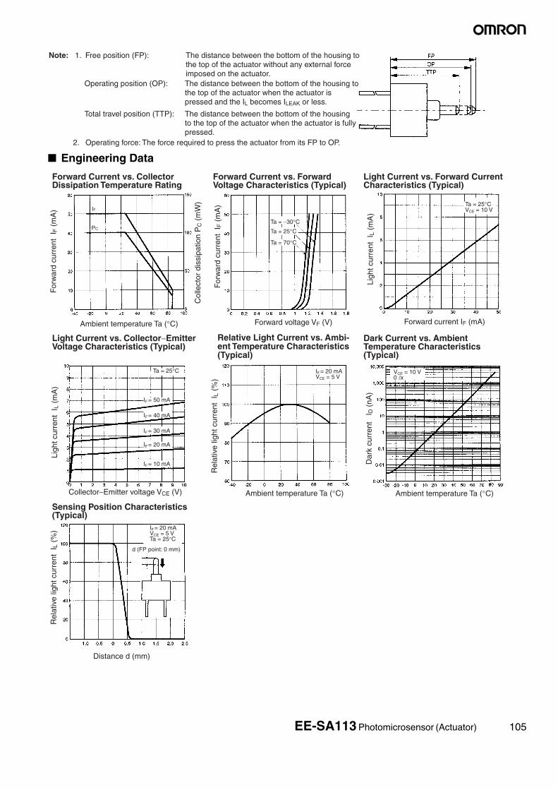
■ Engineering Data2. Operating force: The force required to press the actuator from its FP to OP.
Note: 1. Free position (FP): The distance between the bottom of the housing to the top of the actuator without any external force imposed on the actuator.
Operating position (OP): The distance between the bottom of the housing to the top of the actuator when the actuator is pressed and the IL becomes ILEAK or less.
Total travel position (TTP): The distance between the bottom of the housing to the top of the actuator when the actuator is fully pressed.
Forward Current vs. Collector Dissipation Temperature Rating
Forward Current vs. Forward Voltage Characteristics (Typical)
Light Current vs. Forward Current Characteristics (Typical)
Light Current vs. Collector−Emitter Voltage Characteristics (Typical)
Dark Current vs. Ambient Temperature Characteristics (Typical)
Sensing Position Characteristics (Typical)
Distance d (mm)
d (FP point: 0 mm)
Ambient temperature Ta (°C)
Col
lect
or d
issi
patio
n P
C (
mW
)
Forward voltage VF (V)
For
war
d cu
rren
t I F
(m
A)
For
war
d cu
rren
t I F
(m
A)
Forward current IF (mA)
Ligh
t cur
rent
IL
(mA
)
Collector−Emitter voltage VCE (V)
Ligh
t cur
rent
IL
(mA
)
Ambient temperature Ta (°C)
Ta = −30°C
Ta = 25°C
Ta = 70°C
Ta = 25°CVCE = 10 V
IF = 40 mA
IF = 30 mA
IF = 20 mA
IF = 10 mA
Ta = 25°C VCE = 10 V0 lx
IF = 20 mA VCE = 5 V
IF = 20 mA VCE = 5 V Ta = 25°C
Rel
ativ
e lig
ht c
urre
nt I
L (%
)
Dar
k cu
rren
t I D
(nA
)
Rel
ativ
e lig
ht c
urre
nt I
L (%
)
IF = 50 mA
Ambient temperature Ta (°C)
IF
PC
Relative Light Current vs. Ambi-ent Temperature Characteristics (Typical)
EE-SA113 Photomicrosensor (Actuator) 105

Photomicrosensor (Transmissive)
EE-SG3/EE-SG3-BBe sure to read Precautions on page 25.
■ DimensionsNote: All units are in millimeters unless otherwise indicated.
■ Features• Dust-proof model.• Solder terminal model (EE-SG3).• PCB terminal model (EE-SG3-B).
■ Absolute Maximum Ratings (Ta = 25°C)
Note: 1. Refer to the temperature rating chart if the ambient temper-ature exceeds 25°C.
2. The pulse width is 10 μs maximum with a frequency of100 Hz.
3. Complete soldering within 10 seconds.
■ Electrical and Optical Characteristics (Ta = 25°C)
Internal Circuit
K
A
C
E
Terminal No. Name
A Anode
K Cathode
C Collector
E Emitter
Dimensions Tolerance
3 mm max. ±0.3
3 < mm ≤ 6 ±0.375
6 < mm ≤ 10 ±0.45
10 < mm ≤ 18 ±0.55
18 < mm ≤ 30 ±0.65
Unless otherwise specified, the tolerances are as shown below.
Four, 1.5
Four, 0.5
Optical axis
Cross section AA
Cross section AA
Four, 0.25
19±0.125.4±0.2
3.6±0.2
7.62±0.32.54±0.3
2.54
0.8 0.6
1.2
13Two, 3.2±0.2 dia. holes
Item Symbol Rated value
Emitter Forward current IF 50 mA (see note 1)
Pulse forward cur-rent
IFP 1 A (see note 2)
Reverse voltage VR 4 V
Detector Collector–Emitter voltage
VCEO 30 V
Emitter–Collector voltage
VECO ---
Collector current IC 20 mA
Collector dissipa-tion
PC 100 mW (see note 1)
Ambient tem-perature
Operating Topr –25°C to 85°CStorage Tstg –30°C to 100°C
Soldering temperature Tsol 260°C(see note 3)
Item Symbol Value Condition
Emitter Forward voltage VF 1.2 V typ., 1.5 V max. IF = 30 mA
Reverse current IR 0.01 μA typ., 10 μA max. VR = 4 V
Peak emission wavelength λP 940 nm typ. IF = 20 mA
Detector Light current IL 2 mA min., 40 mA max. IF = 15 mA, VCE = 10 V
Dark current ID 2 nA typ., 200 nA max. VCE = 10 V, 0 lx
Leakage current ILEAK --- ---
Collector–Emitter saturated volt-age
VCE (sat) 0.1 V typ., 0.4 V max. IF = 30 mA, IL = 1 mA
Peak spectral sensitivity wave-length
λP 850 nm typ. VCE = 10 V
Rising time tr 4 μs typ. VCC = 5 V, RL = 100 Ω, IL = 5 mA
Falling time tf 4 μs typ. VCC = 5 V, RL = 100 Ω, IL = 5 mA
106 EE-SG3/EE-SG3-B Photomicrosensor (Transmissive)

■ Engineering Data
Forward Current vs. Collector Dissipation Temperature Rating
Forward Current vs. Forward Voltage Characteristics (Typical)
Light Current vs. Forward Current Characteristics (Typical)
Light Current vs. Collector−Emitter Voltage Characteristics (Typical)
Dark Current vs. Ambient Temperature Characteristics (Typical)
Distance d (mm)
Input
Output
Input
Output
90 %10 %
(Center of optical axis)
Sensing Position Characteristics (Typical)
Response Time Measurement Circuit
Ambient temperature Ta (°C)
Col
lect
or d
issi
patio
n P
C (
mW
)
Forward voltage VF (V)
For
war
d cu
rren
t I F
(m
A)
For
war
d cu
rren
t I F
(m
A)
Forward current IF (mA)
Ligh
t cur
rent
IL
(mA
)Collector−Emitter voltage VCE (V)
Ligh
t cur
rent
IL
(mA
)
Ambient temperature Ta (°C)
Load resistance RL (kΩ)
Ta = −30°C
Ta = 25°C
Ta = 70°C
Ta = 25°CVCE = 10 V
IF = 20 mA
IF = 15 mA
IF = 10 mA
IF = 5 mA
Ta = 25°C VCE = 10 V0 lx
IF = 20 mA VCE = 5 V
IF = 20 mA VCE = 10 V Ta = 25°C
VCC = 5 V Ta = 25°C
Res
pons
e tim
e tr,
tf (
μs)
Rel
ativ
e lig
ht c
urre
nt I
L (%
)
Dar
k cu
rren
t I D
(nA
)
Rel
ativ
e lig
ht c
urre
nt I
L (%
)
IF = 25 mA
Ambient temperature Ta (°C)
IF
PC
Relative Light Current vs. Ambi-ent Temperature Characteristics (Typical)
Response Time vs. Load Resist-ance Characteristics (Typical)
Distance d (mm)
Sensing Position Characteristics (Typical)
Rel
ativ
e lig
ht c
urre
nt I
L (%
)
100
80
60
40
20
0−1.5−2.0 −1.0 −0.5 0 0.5 1.0 1.5 2.0
120
d
IF = 20 mA VCE = 10 V Ta = 25°C
(Cen
ter
of o
ptic
al a
xis)
EE-SG3/EE-SG3-B Photomicrosensor (Transmissive) 107
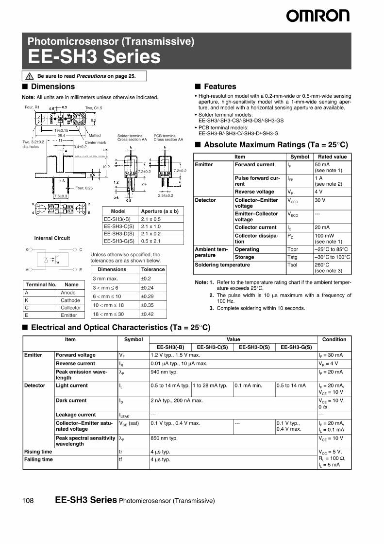
Photomicrosensor (Transmissive)
EE-SH3 SeriesBe sure to read Precautions on page 25.
■ DimensionsNote: All units are in millimeters unless otherwise indicated.
■ Features• High-resolution model with a 0.2-mm-wide or 0.5-mm-wide sensing
aperture, high-sensitivity model with a 1-mm-wide sensing aper-ture, and model with a horizontal sensing aperture are available.
• Solder terminal models:EE-SH3/-SH3-CS/-SH3-DS/-SH3-GS
• PCB terminal models:EE-SH3-B/-SH3-C/-SH3-D/-SH3-G
■ Absolute Maximum Ratings (Ta = 25°C)
Note: 1. Refer to the temperature rating chart if the ambient temper-ature exceeds 25°C.
2. The pulse width is 10 μs maximum with a frequency of100 Hz.
3. Complete soldering within 10 seconds.
■ Electrical and Optical Characteristics (Ta = 25°C)
Internal Circuit
K
A
C
E
Terminal No. Name
A Anode
K Cathode
C Collector
E Emitter
Dimensions Tolerance
3 mm max. ±0.2
3 < mm ≤ 6 ±0.24
6 < mm ≤ 10 ±0.29
10 < mm ≤ 18 ±0.35
18 < mm ≤ 30 ±0.42
Four, 0.25
Two, C1.5Four, R1
Matted
Center mark
Solder terminalCross section AA
PCB terminalCross section AA
19±0.1525.4
3.4±0.2
2.54±0.2
7.2±0.2 7.2±0.2
7.6±0.3
6.2
10.2
Model Aperture (a x b)
EE-SH3(-B) 2.1 x 0.5 EE-SH3-C(S) 2.1 x 1.0
EE-SH3-D(S) 2.1 x 0.2
EE-SH3-G(S) 0.5 x 2.1
Unless otherwise specified, the tolerances are as shown below.
Two, 3.2±0.2 dia. holes
Item Symbol Rated value
Emitter Forward current IF 50 mA (see note 1)
Pulse forward cur-rent
IFP 1 A (see note 2)
Reverse voltage VR 4 V
Detector Collector–Emitter voltage
VCEO 30 V
Emitter–Collector voltage
VECO ---
Collector current IC 20 mA
Collector dissipa-tion
PC 100 mW (see note 1)
Ambient tem-perature
Operating Topr –25°C to 85°CStorage Tstg –30°C to 100°C
Soldering temperature Tsol 260°C(see note 3)
Item Symbol Value Condition
EE-SH3(-B) EE-SH3-C(S) EE-SH3-D(S) EE-SH3-G(S)
Emitter Forward voltage VF 1.2 V typ., 1.5 V max. IF = 30 mA
Reverse current IR 0.01 μA typ., 10 μA max. VR = 4 V
Peak emission wave-length
λP 940 nm typ. IF = 20 mA
Detector Light current IL 0.5 to 14 mA typ. 1 to 28 mA typ. 0.1 mA min. 0.5 to 14 mA IF = 20 mA, VCE = 10 V
Dark current ID 2 nA typ., 200 nA max. VCE = 10 V, 0 lx
Leakage current ILEAK --- ---
Collector–Emitter satu-rated voltage
VCE (sat) 0.1 V typ., 0.4 V max. --- 0.1 V typ., 0.4 V max.
IF = 20 mA, IL = 0.1 mA
Peak spectral sensitivity wavelength
λP 850 nm typ. VCE = 10 V
Rising time tr 4 μs typ. VCC = 5 V,RL = 100 Ω, IL = 5 mA
Falling time tf 4 μs typ.
108 EE-SH3 Series Photomicrosensor (Transmissive)

■ Engineering Data
Forward Current vs. Collector Dissipation Temperature Rating
Forward Current vs. Forward Voltage Characteristics (Typical)
Light Current vs. Forward Current Characteristics (Typical)
Light Current vs. Collector−Emitter Voltage Characteristics (EE-SH3(-B))
Dark Current vs. Ambient Temperature Characteristics (Typical)
Sensing Position Characteristics (EE-SH3-D(S))
Distance d (mm)
Sensing Position Characteristics (EE-SH3(-B))
Distance d (mm)
Sensing Position Characteristics (EE-SH3-G(S))
Distance d (mm)
Sensing Position Characteristics (EE-SH3-C(S))
Distance d (mm)
Input
Output
Input
Output
90 %10 %
Center of optical axisCenter of optical axis
Center of optical axis
Center of optical axis
d
0
−
+
Response Time Measurement Circuit
Ambient temperature Ta (°C)
Col
lect
or d
issi
patio
n P
C (
mW
)
Forward voltage VF (V)
For
war
d cu
rren
t I F
(m
A)
For
war
d cu
rren
t I F
(m
A)
Forward current IF (mA)
Ligh
t cur
rent
IL
(mA
)
Collector−Emitter voltage VCE (V)
Ligh
t cur
rent
IL
(mA
)
Ambient temperature Ta (°C)
Load resistance RL (kΩ)
Ta = −30°C
Ta = 25°C
Ta = 70°C
Ta = 25°CVCE = 10 V
IF = 40 mA
IF = 30 mA
IF = 20 mA
IF = 10 mA
Ta = 25°C VCE = 10 V0 lx
IF = 20 mA VCE = 5 V
IF = 20 mA VCE = 10 V Ta = 25°C
VCC = 5 V Ta = 25°C
Res
pons
e tim
e tr,
tf (
μs)
Rel
ativ
e lig
ht c
urre
nt I
L (%
)
Dar
k cu
rren
t I D
(nA
)
IF = 50 mA
Ambient temperature Ta (°C)
IF
PC
Rel
ativ
e lig
ht c
urre
nt I
L (%
) IF = 20 mA VCE = 10 V Ta = 25°C
Rel
ativ
e lig
ht c
urre
nt I
L (%
)
IF = 20 mA VCE = 10 V Ta = 25°C
Rel
ativ
e lig
ht c
urre
nt I
L (%
) IF = 20 mA VCE = 10 V Ta = 25°C
Rel
ativ
e lig
ht c
urre
nt I
L (%
)Relative Light Current vs. Ambi-ent Temperature Characteristics (Typical)
Response Time vs. Load Resist-ance Characteristics (Typical)
EE-SH3 Series Photomicrosensor (Transmissive) 109

Photomicrosensor (Transmissive)
EE-SJ3 SeriesBe sure to read Precautions on page 25.
■ DimensionsNote: All units are in millimeters unless otherwise indicated.
■ Features• High-resolution model with a 0.2-mm-wide sensing aperture, high-
sensitivity model with a 1-mm-wide sensing aperture, and modelwith a horizontal sensing aperture are available.
■ Absolute Maximum Ratings (Ta = 25°C)
Note: 1. Refer to the temperature rating chart if the ambient temper-ature exceeds 25°C.
2. The pulse width is 10 μs maximum with a frequency of100 Hz.
3. Complete soldering within 10 seconds.
■ Electrical and Optical Characteristics (Ta = 25°C)
Internal Circuit
K
A
C
E
Terminal No. Name
A AnodeK Cathode
C CollectorE Emitter
Dimensions Tolerance
3 mm max. ±0.3
3 < mm ≤ 6 ±0.375
6 < mm ≤ 10 ±0.45
10 < mm ≤ 18 ±0.55
18 < mm ≤ 30 ±0.65
Model Aperture (a x b)
EE-SJ3-C 2.1 x 1.0EE-SJ3-D 2.1 x 0.2
EE-SJ3-G 0.5 x 2.1
Four, 0.5Four, 0.25
Center mark
Cross section BBCross section AA
7.2±0.2
2.54±0.27.6±0.3
6
0.2
10.2
6.2
0.3
Unless otherwise specified, the tolerances are as shown below.
Item Symbol Rated value
Emitter Forward current IF 50 mA (see note 1)
Pulse forward current
IFP 1 A (see note 2)
Reverse voltage VR 4 V
Detector Collector–Emit-ter voltage
VCEO 30 V
Emitter–Collec-tor voltage
VECO ---
Collector cur-rent
IC 20 mA
Collector dissi-pation
PC 100 mW (see note 1)
Ambient tem-perature
Operating Topr –25°C to 85°CStorage Tstg –30°C to 100°C
Soldering temperature Tsol 260°C(see note 3)
Item Symbol Value Condition
EE-SJ3-C EE-SJ3-D EE-SJ3-G
Emitter Forward voltage VF 1.2 V typ., 1.5 V max. IF = 30 mA
Reverse current IR 0.01 μA typ., 10 μA max. VR = 4 V
Peak emission wave-length
λP 940 nm typ. IF = 20 mA
Detector Light current IL 1 to 28 mA typ. 0.1 mA min. 0.5 to 14 mA IF = 20 mA, VCE = 10 V
Dark current ID 2 nA typ., 200 nA max. VCE = 10 V, 0 lx
Leakage current ILEAK --- ---
Collector–Emitter satu-rated voltage
VCE (sat) 0.1 V typ., 0.4 V max.
--- 0.1 V typ., 0.4 V max.
IF = 20 mA,IL = 0.1 mA
Peak spectral sensitivity wavelength
λP 850 nm typ. VCE = 10 V
Rising time tr 4 μs typ. VCC = 5 V,RL = 100 Ω,IL = 5 mA
Falling time tf 4 μs typ.
110 EE-SJ3 Series Photomicrosensor (Transmissive)

■ Engineering Data
Forward Current vs. Collector Dissipation Temperature Rating
Forward Current vs. Forward Voltage Characteristics (Typical)
Light Current vs. Forward Current Characteristics (Typical)
Light Current vs. Collector−Emitter Voltage Characteristics (EE-SJ3-G)
Dark Current vs. Ambient Temperature Characteristics (Typical)
Sensing Position Characteristics (EE-SJ3-D)
Sensing Position Characteristics (EE-SJ3-G)
Sensing Position Characteristics (EE-SJ3-C)
Distance d (mm)
Input
Output
Input
Output
90 %10 %
Center of optical axis
Center of optical axis
d
0
−
+
Response Time Measurement Circuit
Distance d (mm) Distance d (mm)
Center of optical axis
Ambient temperature Ta (°C)
Col
lect
or d
issi
patio
n P
C (
mW
)
Forward voltage VF (V)
For
war
d cu
rren
t I F
(m
A)
For
war
d cu
rren
t I F
(m
A)
Forward current IF (mA)
Ligh
t cur
rent
IL
(mA
)Collector−Emitter voltage VCE (V)
Ligh
t cur
rent
IL
(mA
)
Ambient temperature Ta (°C)
Load resistance RL (kΩ)
Ta = −30°C
Ta = 25°C
Ta = 70°C
Ta = 25°CVCE = 10 V
IF = 40 mA
IF = 30 mA
IF = 20 mA
IF = 10 mA
Ta = 25°C VCE = 10 V0 lx
IF = 20 mA VCE = 5 V
IF = 20 mA VCE = 10 V Ta = 25°C
VCC = 5 V Ta = 25°C
Res
pons
e tim
e tr,
tf (
μs)
Rel
ativ
e lig
ht c
urre
nt I
L (%
)
Dar
k cu
rren
t I D
(nA
)
IF = 50 mA
Ambient temperature Ta (°C)
IF
PC
Rel
ativ
e lig
ht c
urre
nt I
L (%
) IF = 20 mA VCE = 10 V Ta = 25°C
Rel
ativ
e lig
ht c
urre
nt I
L (%
)
IF = 20 mA VCE = 10 V Ta = 25°C
Rel
ativ
e lig
ht c
urre
nt I
L (%
)
Relative Light Current vs. Ambi-ent Temperature Characteristics (Typical)
Response Time vs. Load Resist-ance Characteristics (Typical)
EE-SJ3 Series Photomicrosensor (Transmissive) 111

Photomicrosensor (Transmissive)
EE-SJ5-BBe sure to read Precautions on page 25.
■ DimensionsNote: All units are in millimeters unless otherwise indicated.
■ Features• General-purpose model with a 5-mm-wide slot.• PCB mounting type.• High resolution with a 0.5-mm-wide aperture.
■ Absolute Maximum Ratings (Ta = 25°C)
Note: 1. Refer to the temperature rating chart if the ambient temper-ature exceeds 25°C.
2. The pulse width is 10 μs maximum with a frequency of100 Hz.
3. Complete soldering within 10 seconds.
■ Electrical and Optical Characteristics (Ta = 25°C)
Internal Circuit
K
A
C
E
Terminal No. Name
A Anode
K Cathode
C Collector
E Emitter
Dimensions Tolerance
3 mm max. ±0.3
3 < mm ≤ 6 ±0.375
6 < mm ≤ 10 ±0.45
10 < mm ≤ 18 ±0.55
18 < mm ≤ 30 ±0.65
Four, 0.5Four, 0.25
Optical axis
Cross section AA
2.1 × 0.5 Aperture holes (see note)
Note: There is no difference in size between the slot on the emitter and that on the detector.
2.54±0.2
7.2±0.2
5±0.2
15.4
9.2±0.3
Unless otherwise specified, the tolerances are as shown below.
Item Symbol Rated value
Emitter Forward current IF 50 mA (see note 1)
Pulse forward cur-rent
IFP 1 A (see note 2)
Reverse voltage VR 4 V
Detector Collector–Emitter voltage
VCEO 30 V
Emitter–Collector voltage
VECO ---
Collector current IC 20 mA
Collector dissipa-tion
PC 100 mW (see note 1)
Ambient tem-perature
Operating Topr –25°C to 85°CStorage Tstg –30°C to 100°C
Soldering temperature Tsol 260°C(see note 3)
Item Symbol Value Condition
Emitter Forward voltage VF 1.2 V typ., 1.5 V max. IF = 30 mA
Reverse current IR 0.01 μA typ., 10 μA max. VR = 4 V
Peak emission wavelength λP 940 nm typ. IF = 20 mA
Detector Light current IL 0.5 mA min., 14 mA max. IF = 20 mA, VCE = 10 V
Dark current ID 2 nA typ., 200 nA max. VCE = 10 V, 0 lx
Leakage current ILEAK --- ---
Collector–Emitter saturated volt-age
VCE (sat) 0.1 V typ., 0.4 V max. IF = 20 mA, IL = 0.1 mA
Peak spectral sensitivity wave-length
λP 850 nm typ. VCE = 10 V
Rising time tr 4 μs typ. VCC = 5 V, RL = 100 Ω, IL = 5 mA
Falling time tf 4 μs typ. VCC = 5 V, RL = 100 Ω, IL = 5 mA
112 EE-SJ5-B Photomicrosensor (Transmissive)

■ Engineering Data
Forward Current vs. Collector Dissipation Temperature Rating
Forward Current vs. Forward Voltage Characteristics (Typical)
Light Current vs. Forward Current Characteristics (Typical)
Light Current vs. Collector−Emitter Voltage Characteristics (Typical)
Dark Current vs. Ambient Temperature Characteristics (Typical)
Distance d (mm)
Input
Output
Input
Output
90 %10 %
(Center of optical axis)
Sensing Position Characteristics (Typical)
Response Time Measurement Circuit
Ambient temperature Ta (°C)
Col
lect
or d
issi
patio
n P
C (
mW
)
Forward voltage VF (V)
For
war
d cu
rren
t I F
(m
A)
For
war
d cu
rren
t I F
(m
A)
Forward current IF (mA)
Ligh
t cur
rent
IL
(mA
)
Collector−Emitter voltage VCE (V)
Ligh
t cur
rent
IL
(mA
)
Ambient temperature Ta (°C)
Load resistance RL (kΩ)
Ta = −30°C
Ta = 25°C
Ta = 70°C
Ta = 25°CVCE = 10 V
IF = 40 mA
IF = 30 mA
IF = 20 mA
IF = 10 mA
Ta = 25°C VCE = 10 V0 lx
IF = 20 mA VCE = 5 V
VCC = 5 V Ta = 25°C
Res
pons
e tim
e tr,
tf (
μs)
Rel
ativ
e lig
ht c
urre
nt I
L (%
)
Dar
k cu
rren
t I D
(nA
)
IF = 50 mA
Ambient temperature Ta (°C)
IF
PC
IF = 20 mA VCE = 10 V Ta = 25°C
Rel
ativ
e lig
ht c
urre
nt I
L (%
)
Relative Light Current vs. Ambi-ent Temperature Characteristics (Typical)
Response Time vs. Load Resist-ance Characteristics (Typical)
Distance d (mm)
Sensing Position Characteristics (Typical)
Rel
ativ
e lig
ht c
urre
nt I
L (%
) 100
80
60
40
20
0−1.5−2.0 −1.0 −0.5 0 0.5 1.0 1.5 2.0
120
d
IF = 20 mA VCE = 10 V Ta = 25°C
(Cen
ter
of o
ptic
al a
xis)
EE-SJ5-B Photomicrosensor (Transmissive) 113

Photomicrosensor (Transmissive)
EE-SV3 SeriesBe sure to read Precautions on page 25.
■ DimensionsNote: All units are in millimeters unless otherwise indicated.
■ Features• High-resolution model with a 0.2-mm-wide or 0.5-mm-wide sensing
aperture, high-sensitivity model with a 1-mm-wide sensing aper-ture, and model with a horizontal sensing aperture are available.
• Solder terminal models:EE-SV3/-SV3-CS/-SV3-DS/-SV3-GS
• PCB terminal modelsEE-SV3-B/-SV3-C/-SV3-D/-SV3-G
■ Absolute Maximum Ratings (Ta = 25°C)
Note: 1. Refer to the temperature rating chart if the ambient temper-ature exceeds 25°C.
2. The pulse width is 10 μs maximum with a frequency of100 Hz.
3. Complete soldering within 10 seconds.
■ Electrical and Optical Characteristics (Ta = 25°C)
Internal Circuit
K
A
C
E
Terminal No. NameA Anode
K CathodeC Collector
E Emitter
Dimensions Tolerance
3 mm max. ±0.2
3 < mm ≤ 6 ±0.24
6 < mm ≤ 10 ±0.29
10 < mm ≤ 18 ±0.35
18 < mm ≤ 30 ±0.42
Model Aperture (a x b)
EE-SV3(-B) 2.1 x 0.5 EE-SV3-C(S) 2.1 x 1.0EE-SV3-D(S) 2.1 x 0.2
EE-SV3-G(S) 0.5 x 2.1
Four, 1.5Four, 0.5
Four, R1Four, R1
Four, 0.25
Center mark
Cross section AA Cross section AA
2.54±0.22.54±0.2
Unless otherwise specified, the tolerances are as shown below.
Two, 3.2±0.2 dia. holes
Two, 3.2±0.2 dia. holes
Item Symbol Rated value
Emitter Forward current IF 50 mA (see note 1)
Pulse forward current
IFP 1 A (see note 2)
Reverse voltage VR 4 V
Detector Collector–Emit-ter voltage
VCEO 30 V
Emitter–Collec-tor voltage
VECO ---
Collector current IC 20 mA
Collector dissipa-tion
PC 100 mW (see note 1)
Ambient tem-perature
Operating Topr –25°C to 85°C
Storage Tstg –30°C to 100°C
Soldering temperature Tsol 260°C(see note 3)
Item Symbol Value Condition
EE-SV3(-B) EE-SV3-C(S) EE-SV3-D(S) EE-SV3-G(S)
Emitter Forward voltage VF 1.2 V typ., 1.5 V max. IF = 30 mA
Reverse current IR 0.01 μA typ., 10 μA max. VR = 4 V
Peak emission wave-length
λP 940 nm typ. IF = 20 mA
Detector Light current IL 0.5 to 14 mA 1 to 28 mA 0.1 mA min. 0.5 to 14 mA IF = 20 mA, VCE = 10 V
Dark current ID 2 nA typ., 200 nA max. VCE = 10 V, 0 lx
Leakage current ILEAK --- ---
Collector–Emitter satu-rated voltage
VCE (sat) 0.1 V typ., 0.4 V max. --- 0.1 V typ., 0.4 V max.
IF = 20 mA, IL = 0.1 mA
Peak spectral sensitivity wavelength
λP 850 nm typ. VCE = 10 V
Rising time tr 4 μs typ. VCC = 5 V,RL = 100 Ω, IL = 5 mA
Falling time tf 4 μs typ.
114 EE-SV3 Series Photomicrosensor (Transmissive)

■ Engineering Data
Forward Current vs. Collector Dissipation Temperature Rating
Forward Current vs. Forward Voltage Characteristics (Typical)
Light Current vs. Forward Current Characteristics (Typical)
Light Current vs. Collector−Emitter Voltage Characteristics (EE-SV3(-B))
Dark Current vs. Ambient Temperature Characteristics (Typical)
Sensing Position Characteristics (EE-SV3-D(S))
Sensing Position Characteristics (EE-SV3(-B))
Sensing Position Characteristics (EE-SV3-G(S))
Sensing Position Characteristics (EE-SV3-C(S))
Input
Output
Input
Output
90 %10 %
Response Time Measurement Circuit
Distance d (mm) Distance d (mm)
Distance d (mm) Distance d (mm)
Center of optical axisCenter of optical axis
Center of optical axis
Center of optical axis
d
0
−
+
Ambient temperature Ta (°C)
Col
lect
or d
issi
patio
n P
C (
mW
)
Forward voltage VF (V)
For
war
d cu
rren
t I F
(m
A)
For
war
d cu
rren
t I F
(m
A)
Forward current IF (mA)
Ligh
t cur
rent
IL
(mA
)
Collector−Emitter voltage VCE (V)
Ligh
t cur
rent
IL
(mA
)
Ambient temperature Ta (°C)
Load resistance RL (kΩ)
Ta = −30°C
Ta = 25°C
Ta = 70°C
Ta = 25°CVCE = 10 V
IF = 40 mA
IF = 30 mA
IF = 20 mA
IF = 10 mA
Ta = 25°C VCE = 10 V0 lx
IF = 20 mA VCE = 5 V
IF = 20 mA VCE = 10 V Ta = 25°C
VCC = 5 V Ta = 25°C
Res
pons
e tim
e tr,
tf (
μs)
Rel
ativ
e lig
ht c
urre
nt I
L (%
)
Dar
k cu
rren
t I D
(nA
)
IF = 50 mA
Ambient temperature Ta (°C)
IF
PC
Rel
ativ
e lig
ht c
urre
nt I
L (%
) IF = 20 mA VCE = 10 V Ta = 25°C
Rel
ativ
e lig
ht c
urre
nt I
L (%
)
IF = 20 mA VCE = 10 V Ta = 25°C
Rel
ativ
e lig
ht c
urre
nt I
L (%
) IF = 20 mA VCE = 10 V Ta = 25°C
Rel
ativ
e lig
ht c
urre
nt I
L (%
)Relative Light Current vs. Ambi-ent Temperature Characteristics (Typical)
Response Time vs. Load Resist-ance Characteristics (Typical)
EE-SV3 Series Photomicrosensor (Transmissive) 115

Photomicrosensor (Transmissive)
EE-SX298Be sure to read Precautions on page 25.
■ DimensionsNote: All units are in millimeters unless otherwise indicated.
■ Features• General-purpose model with a 3-mm-wide slot.• PCB mounting type.• High resolution with a 0.5-mm-wide aperture.• With a Photo-Darlington transistor as a detector element.
■ Absolute Maximum Ratings (Ta = 25°C)
Note: 1. Refer to the temperature rating chart if the ambient temper-ature exceeds 25°C.
2. The pulse width is 10 μs maximum with a frequency of100 Hz.
3. Complete soldering within 10 seconds.
■ Electrical and Optical Characteristics (Ta = 25°C)
Internal Circuit
Terminal No. NameA Anode
K CathodeC Collector
E Emitter
Four, 0.5±0.1Four, 0.25+0.1
Two, C1±0.3Four, C0.3
Optical axis
Cross section AACross section BB
5±0.1
0.5±0.1
8.5±0.1 10±0.2
6.2±0.5
6.5±0.1
2.5±0.1
12.2±0.3
9.2±0.3
K
A
C
E
Unless otherwise specified, the tolerances are ±0.2 mm.
Item Symbol Rated value
Emitter Forward current IF 50 mA (see note 1)
Pulse forward cur-rent
IFP 1 A (see note 2)
Reverse voltage VR 4 V
Detector Collector–Emitter voltage
VCEO 35 V
Emitter–Collector voltage
VECO ---
Collector current IC 20 mA
Collector dissipa-tion
PC 100 mW (see note 1)
Ambient tem-perature
Operating Topr –25°C to 85°CStorage Tstg –30°C to 100°C
Soldering temperature Tsol 260°C(see note 3)
Item Symbol Value Condition
Emitter Forward voltage VF 1.2 V typ., 1.4 V max. IF = 20 mA
Reverse current IR 0.01 μA typ., 10 μA max. VR = 4 V
Peak emission wavelength λP 940 nm typ. IF = 20 mA
Detector Light current IL 0.5 mA min., 20 mA max. IF = 1 mA, VCE = 2 V
Dark current ID 2 nA typ., 1,000 nA max. VCE = 10 V, 0 lx
Leakage current ILEAK --- ---
Collector–Emitter saturated volt-age
VCE (sat) 0.75 V typ., 1.0 V max. IF = 2 mA, IL = 0.5 mA
Peak spectral sensitivity wave-length
λP 780 nm typ. VCE = 5 V
Rising time tr 70 μs typ. VCC = 5 V, RL = 100 Ω,IL = 10 mA
Falling time tf 70 μs typ. VCC = 5 V, RL = 100 Ω,IL = 10 mA
116 EE-SX298 Photomicrosensor (Transmissive)
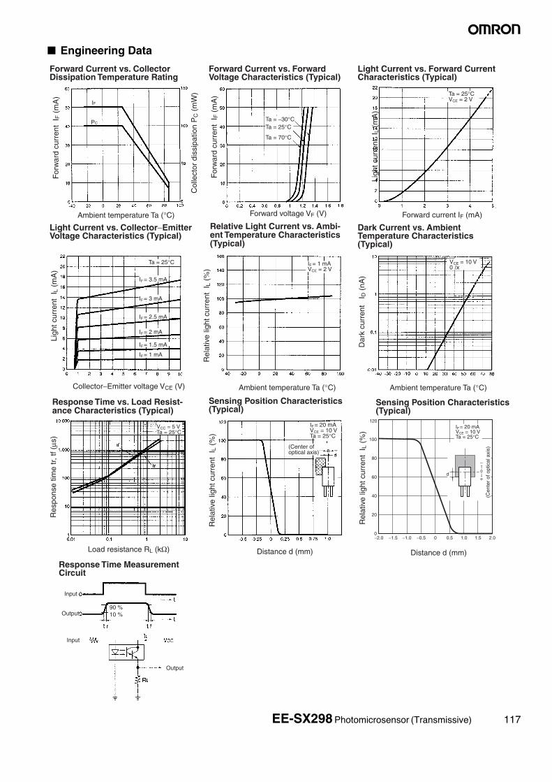
■ Engineering Data
Forward Current vs. Collector Dissipation Temperature Rating
Forward Current vs. Forward Voltage Characteristics (Typical)
Light Current vs. Forward Current Characteristics (Typical)
Light Current vs. Collector−Emitter Voltage Characteristics (Typical)
Dark Current vs. Ambient Temperature Characteristics (Typical)
Distance d (mm)
(Center of optical axis)
90 %10 %
Input
Output
Input
Output
Sensing Position Characteristics (Typical)
Response Time Measurement Circuit
Ambient temperature Ta (°C)
Col
lect
or d
issi
patio
n P
C (
mW
)
Forward voltage VF (V)
For
war
d cu
rren
t I F
(m
A)
For
war
d cu
rren
t I F
(m
A)
Forward current IF (mA)
Ligh
t cur
rent
IL
(mA
)
Collector−Emitter voltage VCE (V)
Ligh
t cur
rent
IL
(mA
)
Ambient temperature Ta (°C)
Load resistance RL (kΩ)
Ta = −30°CTa = 25°C
Ta = 70°C
Ta = 25°CVCE = 2 V
IF = 3 mA
IF = 2.5 mA
IF = 2 mA
IF = 1 mA
Ta = 25°C VCE = 10 V0 lx
IF = 1 mA VCE = 2 V
VCC = 5 V Ta = 25°C
Res
pons
e tim
e tr,
tf (
μs)
Rel
ativ
e lig
ht c
urre
nt I
L (%
)
Dar
k cu
rren
t I D
(nA
)IF = 3.5 mA
Ambient temperature Ta (°C)
IF
PC
IF = 20 mA VCE = 10 V Ta = 25°C
Rel
ativ
e lig
ht c
urre
nt I
L (%
)
IF = 1.5 mA
Relative Light Current vs. Ambi-ent Temperature Characteristics (Typical)
Response Time vs. Load Resist-ance Characteristics (Typical)
100
80
60
40
20
0−1.5−2.0 −1.0 −0.5 0 0.5 1.0 1.5 2.0
120
d
Distance d (mm)
Sensing Position Characteristics (Typical)
Rel
ativ
e lig
ht c
urre
nt I
L (%
)
IF = 20 mA VCE = 10 V Ta = 25°C
(Cen
ter
of o
ptic
al a
xis)
EE-SX298 Photomicrosensor (Transmissive) 117

Photomicrosensor (Transmissive)
EE-SX301/-SX401Be sure to read Precautions on page 25.
■ DimensionsNote: All units are in millimeters unless otherwise indicated.
■ Features• Incorporates an IC chip with a built-in detector element and ampli-
fier.• Incorporates a detector element with a built-in temperature com-
pensation circuit.• A wide supply voltage range: 4.5 to 16 VDC• Directly connects with C-MOS and TTL.• High resolution with a 0.5-mm-wide sensing aperture.• Dark ON model (EE-SX301)• Light ON model (EE-SX401)
■ Absolute Maximum Ratings (Ta = 25°C)
Note: 1. Refer to the temperature rating chart if the ambient temper-ature exceeds 25°C.
2. Complete soldering within 10 seconds.
■ Electrical and Optical Characteristics (Ta = 25°C)
Five, 0.5
Five, 0.25
Cross section AACross section BB
Center mark
Optical axis
Optical axis
Optical axis
2.5±0.2
3.4±0.2
Internal Circuit
Dimensions Tolerance
3 mm max. ±0.3
3 < mm ≤ 6 ±0.375
6 < mm ≤ 10 ±0.45
10 < mm ≤ 18 ±0.55
18 < mm ≤ 30 ±0.65
Terminal No. Name
A AnodeK Cathode
V Power supply (Vcc)
O Output (OUT)
G Ground (GND)
K
A
V
G
O
Unless otherwise specified, the tolerances are as shown below.
Item Symbol Rated value
Emitter Forward current IF 50 mA (see note 1)
Reverse voltage VR 4 V
Detector Power supply volt-age
VCC 16 V
Output voltage VOUT 28 V
Output current IOUT 16 mA
Permissible output dissipation
POUT 250 mW (see note 1)
Ambient tem-perature
Operating Topr –40°C to 75°CStorage Tstg –40°C to 85°C
Soldering temperature Tsol 260°C(see note 2)
Item Symbol Value Condition
Emitter Forward voltage VF 1.2 V typ., 1.5 V max. IF = 20 mA
Reverse current IR 0.01 μA typ., 10 μA max. VR = 4 V
Peak emission wave-length
λP 940 nm typ. IF = 20 mA
Detector Low-level output voltage VOL 0.12 V typ., 0.4 V max. Vcc = 4.5 to 16 V, IOL = 16 mA, IF = 0 mA (EE-SX301), IF = 8 mA (EE-SX401)
High-level output volt-age
VOH 15 V min. Vcc = 16 V, RL = 1 kΩ, IF = 8 mA (EE-SX301), IF = 0 mA (EE-SX401)
Current consumption ICC 3.2 mA typ., 10 mA max. VCC = 16 V
Peak spectral sensitivity wavelength
λP 870 nm typ. VCC = 4.5 to 16 V
LED current when output is OFF IFT 3 mA typ., 8 mA max. VCC = 4.5 to 16 V
LED current when output is ON
Hysteresis ΔH 15% typ. VCC = 4.5 to 16 V (see note 1)
Response frequency f 3 kHz min. VCC = 4.5 to 16 V, IF = 15 mA, IOL = 16 mA (see note 2)
Response delay time tPLH (tPHL) 3 μs typ. VCC = 4.5 to 16 V, IF = 15 mA, IOL = 16 mA (see note 3)
Response delay time tPHL (tPLH) 20 μs typ. VCC = 4.5 to 16 V, IF = 15 mA, IOL = 16 mA (see note 3)
118 EE-SX301/-SX401 Photomicrosensor (Transmissive)

■ Engineering DataNote: The values in the parentheses apply to the EE-SX401.
2.1 mm
0.5 mm0.5 mm Disk
Input
Output
Input
Output
EE-SX301 EE-SX401
Note: 1. Hysteresis denotes the difference in forward LED current value, expressed in percentage, calculated from the respective forward LED currents when the photo IC in turned from ON to OFF and when the photo IC in turned from OFF to ON.
2. The value of the response frequency is measured by rotating the disk as shown below.
3. The following illustrations show the definition of response delay time. The value in the parentheses applies to the EE-SX401.
Forward Current vs. Collector Dissipation Temperature Rating
Forward Current vs. Forward Voltage Characteristics (Typical)
LED Current vs. Supply Voltage (Typical)
Supply voltage VCC (V)
Low-level Output Voltage vs. Output Current (Typical)
Current Consumption vs. Supply Voltage (Typical)
Response Delay Time vs. Forward Current (Typical)
Repeat Sensing Position Characteristics (Typical)
Low
leve
l out
put v
olta
ge V
OL
(V)
Cur
rent
con
sum
ptio
n Ic
c (m
A)
Supply voltage VCC (V) Forward current IF (mA)
Out
put t
rans
isto
r
Distance d (mm)
IFT OFF (IFT ON)
IFT ON (IFT OFF)
VCC = 5 V IF = 0 mA (15 mA)
IOL = 16 mA
IOL = 5 mA
Ta = 25°C IF = 0 mA (15 mA)
VCC = 5 V RL = 330 Ω Ta = 25°C
VOUT
(EE-SX3@@)VOUT
(EE-SX4@@)
Ta = 25°C IF = 15 mAVCC = 5 V RL = 330 Ωn = repeat 20 times
Center of optical axisd1 = 0.01 mm
Ambient temperature Ta (°C)
Out
put a
llow
able
dis
sipa
tion
PC (
mW
)
Forward voltage VF (V)
For
war
d cu
rren
t I F
(m
A)
For
war
d cu
rren
t I F
(m
A)
LED
cur
rent
IF
T (
mA
)
Ta = 25°CRL = 1 kΩ
Res
pons
e de
lay
time
t PH
L, t P
LH (
μs)
IF = 0 mA (15 mA) VCE = 5 V Ta = 25°C
LED
cur
rent
IF
T (
mA
)
IFT OFF (IFT ON)
IFT ON (IFT OFF)
Ambient temperature Ta (°C)
VCC = 5 VRL = 330 Ω
Ta = −30°C
Ta = 25°C
Ta = 70°C
Low
leve
l out
put v
olta
ge V
OL
(V)
Output current IC (mA) Ambient temperature Ta (°C)
Low-level Output Voltage vs. Am-bient Temperature Characteristics (Typical)
LED Current vs. Ambient Temper-ature Characteristics (Typical)
EE-SX301/-SX401 Photomicrosensor (Transmissive) 119

Photomicrosensor (Transmissive)
EE-SX3070/-SX4070Be sure to read Precautions on page 25.
■ DimensionsNote: All units are in millimeters unless otherwise indicated.
■ Features• Incorporates an IC chip with a built-in detector element and ampli-
fier.• Incorporates a detector element with a built-in temperature com-
pensation circuit.• A wide supply voltage range: 4.5 to 16 VDC• Directly connects with C-MOS and TTL.• High resolution with a 0.5-mm-wide sensing aperture.• Dark ON model (EE-SX3070)• Light ON model (EE-SX4070)
■ Absolute Maximum Ratings (Ta = 25°C)
Note: 1. Refer to the temperature rating chart if the ambient temper-ature exceeds 25°C.
2. Complete soldering within 10 seconds.
■ Electrical and Optical Characteristics (Ta = 25°C)
Internal Circuit
Dimensions Tolerance
3 mm max. ±0.3
3 < mm ≤ 6 ±0.375
6 < mm ≤ 10 ±0.45
10 < mm ≤ 18 ±0.55
18 < mm ≤ 30 ±0.65
Terminal No. Name
A Anode
K Cathode
V Power supply (Vcc)
O Output (OUT)
G Ground (GND)
K
A
V
G
O
Optical axis
Five, 0.25Five, 0.5
Two, 0.7
Two, C1
Two, 0.7±0.1 dia.
(1.25)(1.25)
2.35±0.1
(13.8)
Unless otherwise specified, the tolerances are as shown below.
Item Symbol Rated value
Emitter Forward current IF 50 mA (see note 1)
Reverse voltage VR 4 V
Detector Power supply volt-age
VCC 16 V
Output voltage VOUT 28 V
Output current IOUT 16 mA
Permissible output dissipation
POUT 250 mW (see note 1)
Ambient tem-perature
Operating Topr –40°C to 75°CStorage Tstg –40°C to 85°C
Soldering temperature Tsol 260°C(see note 2)
Item Symbol Value Condition
Emitter Forward voltage VF 1.2 V typ., 1.5 V max. IF = 20 mA
Reverse current IR 0.01 μA typ., 10 μA max. VR = 4 V
Peak emission wave-length
λP 940 nm typ. IF = 20 mA
Detector Low-level output voltage VOL 0.12 V typ., 0.4 V max. VCC = 4.5 to 16 V, IOL = 16 mA, IF = 0 mA (EE-SX3070), IF = 10 mA (EE-SX4070)
High-level output volt-age
VOH 15 V min. VCC = 16 V, RL = 1 kΩ, IF = 10 mA (EE-SX3070), IF = 0 mA (EE-SX4070)
Current consumption ICC 3.2 mA typ., 10 mA max. VCC = 16 V
Peak spectral sensitivity wavelength
λP 870 nm typ. VCC = 4.5 to 16 V
LED current when output is OFF IFT 10 mA max. VCC = 4.5 to 16 V
LED current when output is ON
Hysteresis ΔH 15% typ. VCC = 4.5 to 16 V (see note 1)
Response frequency f 3 kHz min. VCC = 4.5 to 16 V, IF = 20 mA, IOL = 16 mA (see note 2)
Response delay time tPLH (tPHL) 3 μs typ. VCC = 4.5 to 16 V, IF = 20 mA, IOL = 16 mA (see note 3)
Response delay time tPHL (tPLH) 20 μs typ. VCC = 4.5 to 16 V, IF = 20 mA, IOL = 16 mA (see note 3)
120 EE-SX3070/-SX4070 Photomicrosensor (Transmissive)

■ Engineering DataNote: The values in the parentheses apply to the EE-SX4070.
2.1 mm
0.5 mm0.5 mm Disk
Input
Output
Input
Output
EE-SX3070 EE-SX4070
Note: 1. Hysteresis denotes the difference in forward LED current value, expressed in percentage, calculated from the respective forward LED currents when the photo IC in turned from ON to OFF and when the photo IC in turned from OFF to ON.
2. The value of the response frequency is measured by rotating the disk as shown below.
3. The following illustrations show the definition of response delay time. The value in the parentheses applies to the EE-SX4070.
Forward Current vs. Collector Dissipation Temperature Rating
Forward Current vs. Forward Voltage Characteristics (Typical)
LED Current vs. Supply Voltage (Typical)
Low-level Output Voltage vs. Output Current (Typical)
Current Consumption vs. Supply Voltage (Typical)
Response Delay Time vs. Forward Current (Typical)
Repeat Sensing Position Characteristics (Typical)
Out
put t
rans
isto
r
Distance d (mm)
Center of optical axis
Supply voltage VCC (V)
Low
leve
l out
put v
olta
ge V
OL
(V)
Cur
rent
con
sum
ptio
n Ic
c (m
A)
Supply voltage VCC (V) Forward current IF (mA)
IFT OFF (IFT ON)
IFT ON (IFT OFF)
VCC = 5 V IF = 0 mA (15 mA)
IOL = 16 mA
IOL = 5 mA
Ta = 25°C IF = 0 mA (15 mA)
VCC = 5 V RL = 330 Ω Ta = 25°C
VOUT
(EE-SX3@@)VOUT
(EE-SX4@@)
Ta = 25°C IF = 15 mAVCC = 5 V RL = 330 Ωn = repeat 20 times
d1 = 0.01 mm
Ambient temperature Ta (°C)
Out
put a
llow
able
dis
sipa
tion
PC (
mW
)
Forward voltage VF (V)
For
war
d cu
rren
t I F
(m
A)
For
war
d cu
rren
t I F
(m
A)
LED
cur
rent
IF
T (
mA
)
Ta = 25°CRL = 1 kΩ
Res
pons
e de
lay
time
t PH
L, t P
LH (
μs)
IF = 0 mA (15 mA) VCC = 5 V Ta = 25°C
LED
cur
rent
IF
T (
mA
)
IFT OFF (IFT ON)
IFT ON (IFT OFF)
Ambient temperature Ta (°C)
VCC = 5 VRL = 330 Ω
Ta = −30°C
Ta = 25°C
Ta = 70°C
Low
leve
l out
put v
olta
ge V
OL
(V)
Output current IC (mA) Ambient temperature Ta (°C)
Low-level Output Voltage vs. Am-bient Temperature Characteristics(Typical)
LED Current vs. Ambient Temper-ature Characteristics (Typical)
EE-SX3070/-SX4070 Photomicrosensor (Transmissive) 121

Photomicrosensor (Transmissive)
EE-SX3081/-SX4081Be sure to read Precautions on page 25.
■ DimensionsNote: All units are in millimeters unless otherwise indicated.
■ Features• Incorporates an IC chip with a built-in detector element and ampli-
fier.• Incorporates a detector element with a built-in temperature com-
pensation circuit.• A wide supply voltage range: 4.5 to 16 VDC• Directly connects with C-MOS and TTL.• High resolution with a 0.5-mm-wide sensing aperture.• Dark ON model (EE-SX3081)• Light ON model (EE-SX4081)
■ Absolute Maximum Ratings (Ta = 25°C)
Note: 1. Refer to the temperature rating chart if the ambient temper-ature exceeds 25°C.
2. Complete soldering within 10 seconds.
■ Electrical and Optical Characteristics (Ta = 25°C)
Internal Circuit
Dimensions Tolerance
3 mm max. ±0.3
3 < mm ≤ 6 ±0.375
6 < mm ≤ 10 ±0.45
10 < mm ≤ 18 ±0.55
18 < mm ≤ 30 ±0.65
Unless otherwise specified, the tolerances are as shown below.
Terminal No. NameA Anode
K Cathode
V Power supply (Vcc)
O Output (OUT)
G Ground (GND)
K
A
V
G
O
Cross section AA
Cross section BB
Optical axis
Four, C0.3
Two, C1±0.3
Five, 0.25±0.1(Five, 0.5±0.1)
8.5±0.1
8.2±0.5
5±0.1
2.5±0.2
2.5+0.16.5±0.1
6.2±0.5
10±0.27.5±0.2
13.7+0.3
(10.5)(2.5)
Item Symbol Rated value
Emitter Forward current IF 50 mA (see note 1)
Reverse voltage VR 4 V
Detector Power supply volt-age
VCC 16 V
Output voltage VOUT 28 V
Output current IOUT 16 mA
Permissible output dissipation
POUT 250 mW (see note 1)
Ambient tem-perature
Operating Topr –40°C to 75°CStorage Tstg –40°C to 85°C
Soldering temperature Tsol 260°C(see note 2)
Item Symbol Value Condition
Emitter Forward voltage VF 1.2 V typ., 1.5 V max. IF = 20 mA
Reverse current IR 0.01 μA typ., 10 μA max. VR = 4 V
Peak emission wave-length
λP 940 nm typ. IF = 20 mA
Detector Low-level output volt-age
VOL 0.12 V typ., 0.4 V max. VCC = 4.5 to 16 V, IOL = 16 mA, IF = 0 mA (EE-SX3081), IF = 8 mA (EE-SX4081)
High-level output volt-age
VOH 15 V min. VCC = 16 V, RL = 1 kΩ, IF = 8 mA (EE-SX3081), IF = 0 mA (EE-SX4081)
Current consumption ICC 3.2 mA typ., 10 mA max. VCC = 16 V
Peak spectral sensitivi-ty wavelength
λP 870 nm typ. VCC = 4.5 to 16 V
LED current when output is OFF IFT 8 mA max. VCC = 4.5 to 16 V
LED current when output is ON
Hysteresis ΔH 15% typ. VCC = 4.5 to 16 V (see note 1)
Response frequency f 3 kHz min. VCC = 4.5 to 16 V, IF = 20 mA, IOL = 16 mA (see note 2)
Response delay time tPLH (tPHL) 3 μs typ. VCC = 4.5 to 16 V, IF = 20 mA, IOL = 16 mA (see note 3)
Response delay time tPHL (tPLH) 20 μs typ. VCC = 4.5 to 16 V, IF = 20 mA, IOL = 16 mA (see note 3)
122 EE-SX3081/-SX4081 Photomicrosensor (Transmissive)

■ Engineering DataNote: The values in the parentheses apply to the EE-SX4081.
2.1 mm
0.5 mm0.5 mm Disk
Input
Output
Input
Output
EE-SX3081 EE-SX4081
Note: 1. Hysteresis denotes the difference in forward LED current value, expressed in percentage, calculated from the respective forward LED currents when the photo IC in turned from ON to OFF and when the photo IC in turned from OFF to ON.
2. The value of the response frequency is measured by rotating the disk as shown below.
3. The following illustrations show the definition of response delay time. The value in the parentheses applies to the EE-SX4081.
Forward Current vs. Collector Dissipation Temperature Rating
Forward Current vs. Forward Voltage Characteristics (Typical)
LED Current vs. Supply Voltage (Typical)
Low-level Output Voltage vs. Output Current (Typical)
Current Consumption vs. Supply Voltage (Typical)
Response Delay Time vs. Forward Current (Typical)
Repeat Sensing Position Characteristics (Typical)
Out
put t
rans
isto
r
Distance d (mm)
Center of optical axis
Supply voltage VCC (V)
Low
leve
l out
put v
olta
ge V
OL
(V)
Cur
rent
con
sum
ptio
n Ic
c (m
A)
Supply voltage VCC (V) Forward current IF (mA)
IFT OFF (IFT ON)
IFT ON (IFT OFF)
VCC = 5 V IF = 0 mA (15 mA)
IOL = 16 mA
IOL = 5 mA
Ta = 25°C IF = 0 mA (15 mA)
VCC = 5 V RL = 330 Ω Ta = 25°C
VOUT
(EE-SX3@@)VOUT
(EE-SX4@@)
Ta = 25°C IF = 15 mAVCC = 5 V RL = 330 Ωn = repeat 20 times
d1 = 0.01 mm
Ambient temperature Ta (°C)
Out
put a
llow
able
dis
sipa
tion
PC (
mW
)
Forward voltage VF (V)
For
war
d cu
rren
t I F
(m
A)
For
war
d cu
rren
t I F
(m
A)
LED
cur
rent
IF
T (
mA
)
Ta = 25°CRL = 1 kΩ
Res
pons
e de
lay
time
t PH
L, t P
LH (
μs)
IF = 0 mA (15 mA) VCC = 5 V Ta = 25°C
LED
cur
rent
IF
T (
mA
)
IFT OFF (IFT ON)
IFT ON (IFT OFF)
Ambient temperature Ta (°C)
VCC = 5 VRL = 330 Ω
Ta = −30°CTa = 25°C
Ta = 70°C
Low
leve
l out
put v
olta
ge V
OL
(V)
Output current IC (mA) Ambient temperature Ta (°C)
Low-level Output Voltage vs. Am-bient Temperature Characteristics (Typical)
LED Current vs. Ambient Temper-ature Characteristics (Typical)
EE-SX3081/-SX4081 Photomicrosensor (Transmissive) 123
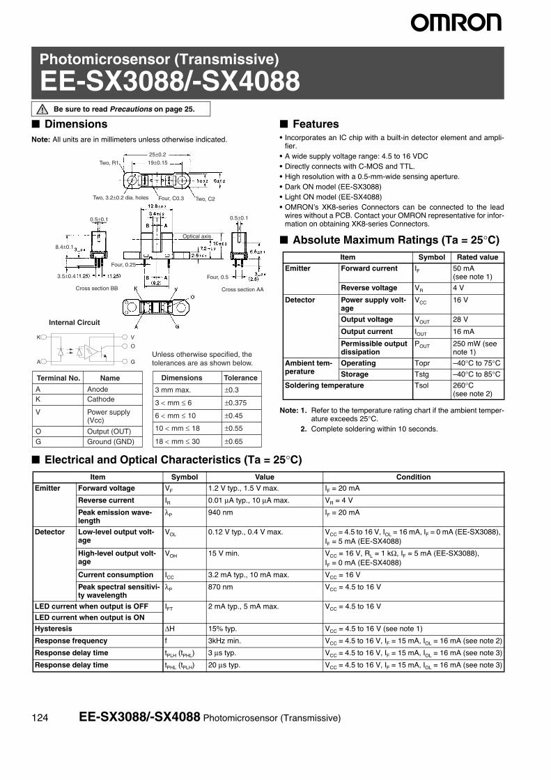
Photomicrosensor (Transmissive)
EE-SX3088/-SX4088Be sure to read Precautions on page 25.
■ DimensionsNote: All units are in millimeters unless otherwise indicated.
■ Features• Incorporates an IC chip with a built-in detector element and ampli-
fier.• A wide supply voltage range: 4.5 to 16 VDC• Directly connects with C-MOS and TTL.• High resolution with a 0.5-mm-wide sensing aperture.• Dark ON model (EE-SX3088)• Light ON model (EE-SX4088)• OMRON’s XK8-series Connectors can be connected to the lead
wires without a PCB. Contact your OMRON representative for infor-mation on obtaining XK8-series Connectors.
■ Absolute Maximum Ratings (Ta = 25°C)
Note: 1. Refer to the temperature rating chart if the ambient temper-ature exceeds 25°C.
2. Complete soldering within 10 seconds.
■ Electrical and Optical Characteristics (Ta = 25°C)
Internal Circuit
Dimensions Tolerance
3 mm max. ±0.3
3 < mm ≤ 6 ±0.375
6 < mm ≤ 10 ±0.45
10 < mm ≤ 18 ±0.55
18 < mm ≤ 30 ±0.65
Terminal No. Name
A AnodeK Cathode
V Power supply (Vcc)
O Output (OUT)G Ground (GND)
K
A
V
G
O
Optical axis
Cross section AACross section BB
Two, R1
Two, C2Four, C0.3
Four, 0.5
Four, 0.25
Two, 3.2±0.2 dia. holes
25±0.2
19±0.15
0.5±0.10.5±0.1
8.4±0.1
3.5±0.4
Unless otherwise specified, the tolerances are as shown below.
Item Symbol Rated value
Emitter Forward current IF 50 mA (see note 1)
Reverse voltage VR 4 V
Detector Power supply volt-age
VCC 16 V
Output voltage VOUT 28 V
Output current IOUT 16 mA
Permissible output dissipation
POUT 250 mW (see note 1)
Ambient tem-perature
Operating Topr –40°C to 75°CStorage Tstg –40°C to 85°C
Soldering temperature Tsol 260°C(see note 2)
Item Symbol Value Condition
Emitter Forward voltage VF 1.2 V typ., 1.5 V max. IF = 20 mA
Reverse current IR 0.01 μA typ., 10 μA max. VR = 4 V
Peak emission wave-length
λP 940 nm IF = 20 mA
Detector Low-level output volt-age
VOL 0.12 V typ., 0.4 V max. VCC = 4.5 to 16 V, IOL = 16 mA, IF = 0 mA (EE-SX3088), IF = 5 mA (EE-SX4088)
High-level output volt-age
VOH 15 V min. VCC = 16 V, RL = 1 kΩ, IF = 5 mA (EE-SX3088), IF = 0 mA (EE-SX4088)
Current consumption ICC 3.2 mA typ., 10 mA max. VCC = 16 V
Peak spectral sensitivi-ty wavelength
λP 870 nm VCC = 4.5 to 16 V
LED current when output is OFF IFT 2 mA typ., 5 mA max. VCC = 4.5 to 16 V
LED current when output is ON
Hysteresis ΔH 15% typ. VCC = 4.5 to 16 V (see note 1)
Response frequency f 3kHz min. VCC = 4.5 to 16 V, IF = 15 mA, IOL = 16 mA (see note 2)
Response delay time tPLH (tPHL) 3 μs typ. VCC = 4.5 to 16 V, IF = 15 mA, IOL = 16 mA (see note 3)
Response delay time tPHL (tPLH) 20 μs typ. VCC = 4.5 to 16 V, IF = 15 mA, IOL = 16 mA (see note 3)
124 EE-SX3088/-SX4088 Photomicrosensor (Transmissive)

■ Engineering DataNote: The values in the parentheses apply to the EE-SX4088.
2.1 mm
0.5 mm0.5 mm Disk
Input
Output
Input
Output
EE-SX3088 EE-SX4088
Note: 1. Hysteresis denotes the difference in forward LED current value, expressed in percentage, calculated from the respective forward LED currents when the photo IC in turned from ON to OFF and when the photo IC in turned from OFF to ON.
2. The value of the response frequency is measured by rotating the disk as shown below.
3. The following illustrations show the definition of response delay time. The value in the parentheses applies to the EE-SX4088.
Forward Current vs. Collector Dissipation Temperature Rating
Forward Current vs. Forward Voltage Characteristics (Typical) (Typical)
Low-level Output Voltage vs. Output Current (Typical)
Current Consumption vs. Supply Voltage (Typical)
Response Delay Time vs. Forward Current (Typical)
Repeat Sensing Position Characteristics (Typical)
Out
put t
rans
isto
r
Distance d (mm)
Center of optical axis
Supply voltage VCC (V)
Low
leve
l out
put v
olta
ge V
OL
(V)
Cur
rent
con
sum
ptio
n Ic
c (m
A)
Supply voltage VCC (V) Forward current IF (mA)
IFT OFF (IFT ON)
IFT ON (IFT OFF)
VCC = 5 V IF = 0 mA (15 mA)
IOL = 16 mA
IOL = 5 mA
Ta = 25°C IF = 0 mA (15 mA)
VCC = 5 V RL = 330 Ω Ta = 25°C
VOUT
(EE-SX3@@)VOUT
(EE-SX4@@)
Ta = 25°C IF = 15 mAVCC = 5 V RL = 330 Ωn = repeat 20 times
d1 = 0.01 mm
Ambient temperature Ta (°C)
Out
put a
llow
able
dis
sipa
tion
PC (
mW
)
Forward voltage VF (V)
For
war
d cu
rren
t I F
(m
A)
For
war
d cu
rren
t I F
(m
A)
LED
cur
rent
IF
T (
mA
)
Ta = 25°CRL = 1 kΩ
Res
pons
e de
lay
time
t PH
L, t P
LH (
μs)
IF = 0 mA (15 mA) VCC = 5 V Ta = 25°C
LED
cur
rent
IF
T (
mA
)
IFT OFF (IFT ON)
IFT ON (IFT OFF)
Ambient temperature Ta (°C)
VCC = 5 VRL = 330 Ω
Ta = −30°C
Ta = 25°C
Ta = 70°C
Low
leve
l out
put v
olta
ge V
OL
(V)
Output current IC (mA) Ambient temperature Ta (°C)
LED Current vs. Supply Voltage
Low-level Output Voltage vs. Am-bient Temperature Characteristics (Typical)
LED Current vs. Ambient Temper-ature Characteristics (Typical)
EE-SX3088/-SX4088 Photomicrosensor (Transmissive) 125

Photo IC Output Photomicrosensor (Transmissive)
EE-SX3148-P1Be sure to read Precautions on page 25.
■ DimensionsNote: All units are in millimeters unless otherwise indicated.
■ Features• A boss on one side enables securing the Sensor with one M2 or M3
screw.• Sensor can be installed from either top of bottom of mounting plate.• High resolution both vertically and horizontally (slot dimensions: 0.5
x 0.5 mm)• 3.6-mm-wide slot.• Photo-IC output connects directly to CMOS and TTL devices.• Applicable to the ZH and ZR Connector Series from JST (Japan
Solderless Terminal).
■ Absolute Maximum Ratings (Ta = 25°C)
Note: Refer to the temperature rating chart if the ambient tempera-ture exceeds 25°C.
■ Electrical and Optical Characteristics (Ta = 25°C, VCC = 5 V ±10%)
26±0.2
20.5±0.1
(13.8)(3.6)
16.4±0.2
11.3±0.2
7.7±0.2
2.6
16.4±0.2
2.6
6.4±0.1
7.5±0.2
3.5
2.9±0.2
1.5
1.5
Four, R0.5
2.5
Two, C0.3
Two, 1.8 dia.
2.5
3.2±0.2 dia.
Japan Solderless Terminal (JST)B3B-ZR
(2)
0.5±0.1
0.5±0.1
0-0.1
Optical axis
1 2 3
Terminal No. Name
1 Power supply (Vcc)
2 Output (OUT)
3 Ground (GND)
Recommended Mating Connectors:JST (Japan Solderless Terminal) ZHR-3 Series (crimp connector)
03ZR Series (press-fit connector)
Dimensions Tolerance
3 mm max. ±0.200
3 < mm ≤ 6 ±0.240
6 < mm ≤ 10 ±0.290
10 < mm ≤ 18 ±0.350
18 < mm ≤ 30 ±0.420
Unless otherwise specified, the tolerances are as shown below.
Item Symbol Rated value
Power supply voltage VCC 6 VDC
Output voltage VOUT 28 V
Output current IOUT 16 mA
Permissible output dissipation POUT 250 mW (see note)
Ambient temperature
Operating Topr –20°C to 75°CStorage Tstg –40°C to 85°C
Soldering temperature Tsol ---
Item Symbol Value Condition
Current consumption ICC 30 mA max. With and without incident
Low-level output voltage VOL 0.3 V max. IOUT = 16 mA without incident
High-level output voltage VOH (VCC x 0.9) V min. VOUT = VCC with incident RL = 47 kΩ
Response frequency f 3 kHz min. VOUT = VCC, RL = 47 kΩ (see note)
Disk
0.5 mm0.5 mm
2.1 mm
Note: The value of the response frequency is measured by rotating the disk as shown below.
126 EE-SX3148-P1 Photo IC Output Photomicrosensor (Transmissive)

■ Engineering Data
300
250
200
150
100
50
0-40 -20 0 20 40 60 80 100 -3
d1
-2 -1 0 1 2 3
d
ON (OFF)
OFF (ON)
ON (OFF)
OFF (ON)
-3
d2
-2 -1 0 1 2 3
d
Output Allowable Dissipation vs. Ambient Temperature Characteristics
Sensing Position Characteristics (Typical)
Out
put a
llow
able
dis
sipa
tion
Pou
t (m
W)
Distance d (mm)Ambient temperature Ta (°C)
Sensing Position Characteristics (Typical)
Out
put t
rans
isto
r
Out
put t
rans
isto
r
Distance d (mm)
d1 = 0±0.3 mm VCC = 5 V Ta = 25°C RL = 47 kΩ
VCC = 5 V Ta = 25°C RL = 47 kΩ
d2 = 0±0.3mm
Ligh
t int
erru
ptin
g pl
ate
(Center of axis)
(Center of axis)
EE-SX3148-P1 Photo IC Output Photomicrosensor (Transmissive) 127

Photomicrosensor (Transmissive)
EE-SX384/-SX484Be sure to read Precautions on page 25.
■ DimensionsNote: All units are in millimeters unless otherwise indicated.
■ Features• Incorporates an IC chip with a built-in detector element and ampli-
fier.• Incorporates a detector element with a built-in temperature com-
pensation circuit.• A wide supply voltage range: 4.5 to 16 VDC• Directly connects with C-MOS and TTL.• High resolution with a 0.5-mm-wide sensing aperture.• Dark ON model (EE-SX384)• Light ON model (EE-SX484)
■ Absolute Maximum Ratings (Ta = 25°C)
Note: 1. Refer to the temperature rating chart if the ambient temper-ature exceeds 25°C.
2. Complete soldering within 10 seconds.
■ Electrical and Optical Characteristics (Ta = 25°C)
Internal Circuit
Unless otherwise specified, the tolerances are ±0.2 mm.
Terminal No. Name
A Anode
K Cathode
V Power supply (Vcc)
O Output (OUT)G Ground (GND)
K
A
V
G
0
Cross section AACross section BB
7 min. Five, 0.5
Five, 0.252.5
8 5.5
0.50.5
5.5
1.25 1.25
Item Symbol Rated value
Emitter Forward current IF 50 mA (see note 1)
Reverse voltage VR 4 V
Detector Power supply volt-age
VCC 16 V
Output voltage VOUT 28 V
Output current IOUT 16 mA
Permissible output dissipation
POUT 250 mW (see note 1)
Ambient tem-perature
Operating Topr –40°C to 75°CStorage Tstg –40°C to 85°C
Soldering temperature Tsol 260°C(see note 2)
Item Symbol Value Condition
Emitter Forward voltage VF 1.2 V typ., 1.5 V max. IF = 20 mA
Reverse current IR 0.01 μA typ., 10 μA max. VR = 4 V
Peak emission wave-length
λP 940 nm typ. IF = 20 mA
Detector Low-level output volt-age
VOL 0.12 V typ., 0.4 V max. VCC = 4.5 to 16 V, IOL = 16 mA, IF = 0 mA (EE-SX384), IF = 8 mA (EE-SX484)
High-level output volt-age
VOH 15 V min. VCC = 16 V, RL = 1 kΩ, IF = 8 mA (EE-SX384), IF = 0 mA (EE-SX484)
Current consumption ICC 3.2 mA typ., 10 mA max. VCC = 16 V
Peak spectral sensitivi-ty wavelength
λP 870 nm typ. VCC = 4.5 to 16 V
LED current when output is OFF IFT 3 mA typ., 8 mA max. VCC = 4.5 to 16 V
LED current when output is ON
Hysteresis ΔH 15% typ. VCC = 4.5 to 16 V (see note 1)
Response frequency f 3 kHz min. VCC = 4.5 to 16 V, IF = 15 mA, IOL = 16 mA (see note 2)
Response delay time tPLH (tPHL) 3 μs typ. VCC = 4.5 to 16 V, IF = 15 mA, IOL = 16 mA (see note 3)
Response delay time tPHL (tPLH) 20 μs typ. VCC = 4.5 to 16 V, IF = 15 mA, IOL = 16 mA (see note 3)
128 EE-SX384/-SX484 Photomicrosensor (Transmissive)

■ Engineering DataNote: The values in the parentheses apply to the EE-SX484.
2.1 mm
0.5 mm0.5 mm Disk
Input
Output
Input
Output
EE-SX384 EE-SX484
Note: 1. Hysteresis denotes the difference in forward LED current value, expressed in percentage, calculated from the respective forward LED currents when the photo IC in turned from ON to OFF and when the photo IC in turned from OFF to ON.
2. The value of the response frequency is measured by rotating the disk as shown below.
3. The following illustrations show the definition of response delay time. The value in the parentheses applies to the EE-SX484.
Forward Current vs. Collector Dissipation Temperature Rating
Forward Current vs. Forward Voltage Characteristics (Typical)
LED Current vs. Supply Voltage (Typical)
Low-level Output Voltage vs. Output Current (Typical)
Current Consumption vs. Supply Voltage (Typical)
Response Delay Time vs. Forward Current (Typical)
Repeat Sensing Position Characteristics (Typical)
Out
put t
rans
isto
r
Distance d (mm)
Center of optical axis
Supply voltage VCC (V)
Low
leve
l out
put v
olta
ge V
OL
(V)
Cur
rent
con
sum
ptio
n Ic
c (m
A)
Supply voltage VCC (V) Forward current IF (mA)
IFT OFF (IFT ON)
IFT ON (IFT OFF)
VCC = 5 V IF = 0 mA (15 mA)
IOL = 16 mA
IOL = 5 mA
Ta = 25°C IF = 0 mA (15 mA)
VCC = 5 V RL = 330 Ω Ta = 25°C
VOUT
(EE-SX3@@)VOUT
(EE-SX4@@)
Ta = 25°C IF = 15 mAVCC = 5 V RL = 330 Ω
d1 = 0.01 mm
Ambient temperature Ta (°C)
Out
put a
llow
able
dis
sipa
tion
PC (
mW
)
Forward voltage VF (V)
For
war
d cu
rren
t I F
(m
A)
For
war
d cu
rren
t I F
(m
A)
LED
cur
rent
IF
T (
mA
)
Ta = 25°CRL = 1 kΩ
Res
pons
e de
lay
time
t PH
L, t P
LH (
μs)
IF = 0 mA (15 mA) VCC = 5 V Ta = 25°C
LED
cur
rent
IF
T (
mA
)
IFT OFF (IFT ON)
IFT ON (IFT OFF)
Ambient temperature Ta (°C)
VCC = 5 VRL = 330 Ω
Ta = −30°C
Ta = 25°C
Ta = 70°C
Low
leve
l out
put v
olta
ge V
OL
(V)
Output current IC (mA) Ambient temperature Ta (°C)
Low-level Output Voltage vs. Am-bient Temperature Characteristics (Typical)
LED Current vs. Ambient Temper-ature Characteristics (Typical)
n = repeat 20 times
EE-SX384/-SX484 Photomicrosensor (Transmissive) 129

Photomicrosensor (Transmissive)
EE-SX493Be sure to read Precautions on page 25.
■ DimensionsNote: All units are in millimeters unless otherwise indicated.
■ Features• Incorporates an IC chip with a built-in detector element and ampli-
fier.• Incorporates a detector element with a built-in temperature com-
pensation circuit.• A wide supply voltage range: 4.5 to 16 VDC• Directly connects with C-MOS and TTL.• Allows highly precise sensing with a 0.2-mm-wide sensing aper-
ture.
■ Absolute Maximum Ratings (Ta = 25°C)
Note: 1. Refer to the temperature rating chart if the ambient temper-ature exceeds 25°C.
2. Complete soldering within 10 seconds.
■ Electrical and Optical Characteristics (Ta = 25°C)
Internal Circuit
Dimensions Tolerance
3 mm max. ±0.125
3 < mm ≤ 6 ±0.150
6 < mm ≤ 10 ±0.180
10 < mm ≤ 18 ±0.215
18 < mm ≤ 30 ±0.260
Terminal No. Name
A Anode
K Cathode
V Power supply (Vcc)
O Output (OUT)
G Ground (GND)
K
A
V
G
O
Cross section AA
Cross section BB
Five, 0.5Five, 0.25
Two, 1 0−0.2 dia.
6
0.2
7±0.1
0.75±0.1
6.9±0.5
6.5±0.05
(1.25)(1.25)
9.5
Pull-off taper: 1/25 max.
(Tip dimension)
Unless otherwise specified, the tolerances are as shown below.
Item Symbol Rated value
Emitter Forward current IF 50 mA (see note 1)
Reverse voltage VR 4 V
Detector Power supply volt-age
VCC 16 V
Output voltage VOUT 28 V
Output current IOUT 16 mA
Permissible output dissipation
POUT 250 mW (see note 1)
Ambient tem-perature
Operating Topr –40°C to 60°CStorage Tstg –40°C to 85°C
Soldering temperature Tsol 260°C(see note 2)
Item Symbol Value Condition
Emitter Forward voltage VF 1.2 V typ., 1.5 V max. IF = 20 mA
Reverse current IR 0.01 μA typ., 10 μA max. VR = 4 V
Peak emission wavelength λP 940 nm typ. IF = 20 mA
Detector Low-level output voltage VOL 0.12 V typ., 0.4 V max. VCC = 4.5 to 16 V, IOL = 16 mA, IF = 15 mA
High-level output voltage VOH 15 V min. VCC = 16 V, RL = 1 kΩ, IF = 0 mA
Current consumption ICC 5 mA typ., 10 mA max. VCC = 16 V
Peak spectral sensitivity wavelength
λP 870 nm typ. VCC = 4.5 to 16 V
LED current when output is OFF IFT 10 mA typ., 15 mA max. VCC = 4.5 to 16 V
LED current when output is ON
Hysteresis ΔH 15% typ. VCC = 4.5 to 16 V (see note 1)
Response frequency f 3 kHz min. VCC = 4.5 to 16 V, IF = 15 mA, IOL = 16 mA (see note 2)
Response delay time tPLH (tPHL) 3 μs typ. VCC = 4.5 to 16 V, IF = 15 mA, IOL = 16 mA (see note 3)
Response delay time tPHL (tPLH) 20 μs typ. VCC = 4.5 to 16 V, IF = 15 mA, IOL = 16 mA (see note 3)
130 EE-SX493 Photomicrosensor (Transmissive)

■ Engineering Data
2.1 mm
0.2 mm0.2 mm Disk
Input
Output
Note: 1. Hysteresis denotes the difference in forward LED current value, expressed in percentage, calculated from the respective forward LED currents when the photo IC in turned from ON to OFF and when the photo IC in turned from OFF to ON.
2. The value of the response frequency is measured by rotating the disk as shown below.
3. The following illustrations show the definition of response delay time.
Forward Current vs. Collector Dissipation Temperature Rating
Forward Current vs. Forward Voltage Characteristics (Typical)
LED Current vs. Supply Voltage (Typical)
Low-level Output Voltage vs. Output Current (Typical)
Current Consumption vs. Supply Voltage (Typical)
Response Delay Time vs. Forward Current (Typical)
Repeat Sensing Position Characteristics (Typical)
Out
put t
rans
isto
r
Distance d (mm)
Supply voltage VCC (V)
Low
leve
l out
put v
olta
ge V
OL
(V)
Cur
rent
con
sum
ptio
n Ic
c (m
A)
Supply voltage VCC (V) Forward current IF (mA)
IFT ON
IFT OFF
VCC = 5 V IF = 15 mA
IOL = 16 mA
IOL = 5 mA
Ta = 25°C IF = 15 mA
Ta = 25°C IF = 15 mAVCC = 5 V RL = 330 Ωn = repeat 20 times
d1 = 0.01 mm
Ambient temperature Ta (°C)
Out
put a
llow
able
dis
sipa
tion
PC (
mW
)
Forward voltage VF (V)
For
war
d cu
rren
t I F
(m
A)
For
war
d cu
rren
t I F
(m
A)
LED
cur
rent
IF
T (
mA
)
Ta = 25°CRL = 1 kΩ
Res
pons
e de
lay
time
t PH
L, t P
LH (
μs)
IF = 15 mAVCC = 5 V Ta = 25°C
LED
cur
rent
IF
T (
mA
) IFT ON
IFT OFF
Ambient temperature Ta (°C)
VCC = 5 VRL = 330 Ω
Ta = −30°C
Ta = 25°C
Ta = 70°C
Low
leve
l out
put v
olta
ge V
OL
(V)
Output current IC (mA) Ambient temperature Ta (°C)
Low-level Output Voltage vs. Am-bient Temperature Characteristics (Typical)
LED Current vs. Ambient Temper-ature Characteristics (Typical)
40
35
30
25
20
15
10
5
00 40205 10 15 25 30 35
tPHL (tPLH)
tPLH (tPHL)
VOUT
(EE-SX4@@)tPHL tPLH
t
tIF
VCC
OUT
GND
IF ICC
VOUT
RL
VCC = 5 V RL = 330 Ω
EE-SX493 Photomicrosensor (Transmissive) 131

Photomicrosensor (Transmissive)
EE-SX398/498Be sure to read Precautions on page 25.
■ DimensionsNote: All units are in millimeters unless otherwise indicated.
■ Features• Incorporates an IC chip with a built-in detector element and ampli-
fier.• Incorporates a detector element with a built-in temperature com-
pensation circuit.• A wide supply voltage range: 4.5 to 16 VDC• Directly connects with C-MOS and TTL.• High resolution with a 0.5-mm-wide sensing aperture.• Dark ON model (EE-SX398)• Light ON model (EE-SX498)
■ Absolute Maximum Ratings (Ta = 25°C)
Note: 1. Refer to the temperature rating chart if the ambient temper-ature exceeds 25°C.
2. Complete soldering within 10 seconds.
■ Electrical and Optical Characteristics (Ta = 25°C)
Internal Circuit
Dimensions Tolerance
3 mm max. ±0.3
3 < mm ≤ 6 ±0.375
6 < mm ≤ 10 ±0.45
10 < mm ≤ 18 ±0.55
18 < mm ≤ 30 ±0.65
Terminal No. Name
A Anode
K Cathode
V Power supply (Vcc)
O Output (OUT)G Ground (GND)
K
A
V
G
O
Optical axis
Cross section AACross section BB
Two, C1±0.3
Five, 0.5±0.1
Five, 0.25±0.1
Four, C0.3
12.2±0.3
0.5±0.1
8.5±0.5
8.2±0.5
10±0.2
6.2±0.5
6.5±0.1
(2.5)(9.2)
Unless otherwise specified, the tolerances are as shown below.
Item Symbol Rated value
Emitter Forward current IF 50 mA (see note 1)
Reverse voltage VR 4 V
Detector Power supply volt-age
VCC 16 V
Output voltage VOUT 28 V
Output current IOUT 16 mA
Permissible output dissipation
POUT 250 mW (see note 1)
Ambient tem-perature
Operating Topr –40°C to 75°CStorage Tstg –40°C to 85°C
Soldering temperature Tsol 260°C(see note 2)
Item Symbol Value Condition
Emitter Forward voltage VF 1.2 V typ., 1.5 V max. IF = 20 mA
Reverse current IR 0.01 μA typ., 10 μA max. VR = 4 V
Peak emission wave-length
λP 940 nm typ. IF = 20 mA
Detector Low-level output volt-age
VOL 0.12 V typ., 0.4 V max. VCC = 4.5 to 16 V, IOL = 16 mA, IF = 0 mA (EE-SX398), IF = 5 mA (EE-SX498)
High-level output volt-age
VOH 15 V min. VCC = 16 V, RL = 1 kΩ, IF = 5 mA (EE-SX398), IF = 0 mA (EE-SX498)
Current consumption ICC 3.2 mA typ., 10 mA max. VCC = 16 V
Peak spectral sensitivi-ty wavelength
λP 870 nm typ. VCC = 4.5 to 16 V
LED current when output is OFF IFT 2 mA typ., 5 mA max. VCC = 4.5 to 16 V
LED current when output is ON
Hysteresis ΔH 15% typ. VCC = 4.5 to 16 V (see note 1)
Response frequency f 3 kHz min. VCC = 4.5 to 16 V, IF = 15 mA, IOL = 16 mA (see note 2)
Response delay time tPLH (tPHL) 3 μs typ. VCC = 4.5 to 16 V, IF = 15 mA, IOL = 16 mA (see note 3)
Response delay time tPHL (tPLH) 20 μs typ. VCC = 4.5 to 16 V, IF = 15 mA, IOL = 16 mA (see note 3)
132 EE-SX398/498 Photomicrosensor (Transmissive)

■ Engineering DataNote: The values in the parentheses apply to the EE-SX498.
2.1 mm
0.5 mm0.5 mm Disk
Input
Output
Input
Output
EE-SX398 EE-SX498
Note: 1. Hysteresis denotes the difference in forward LED current value, expressed in percentage, calculated from the respective forward LED currents when the photo IC in turned from ON to OFF and when the photo IC in turned from OFF to ON.
2. The value of the response frequency is measured by rotating the disk as shown below.
3. The following illustrations show the definition of response delay time. The value in the parentheses applies to the EE-SX498.
Forward Current vs. Collector Dissipation Temperature Rating
Forward Current vs. Forward Voltage Characteristics (Typical)
LED Current vs. Supply Voltage (Typical)
Low-level Output Voltage vs. Output Current (Typical)
Current Consumption vs. Supply Voltage (Typical)
Response Delay Time vs. Forward Current (Typical)
Repeat Sensing Position Characteristics (Typical)
Out
put t
rans
isto
r
Distance d (mm)
Center of optical axis
Supply voltage VCC (V)
Low
leve
l out
put v
olta
ge V
OL
(V)
Cur
rent
con
sum
ptio
n Ic
c (m
A)
Supply voltage VCC (V) Forward current IF (mA)
IFT OFF (IFT ON)
IFT ON (IFT OFF)
VCC = 5 V IF = 0 mA (15 mA)
IOL = 16 mA
IOL = 5 mA
Ta = 25°C IF = 0 mA (15 mA)
VCC = 5 V RL = 330 Ω Ta = 25°C
VOUT
(EE-SX3@@)VOUT
(EE-SX4@@)
Ta = 25°C IF = 15 mAVCC = 5 V RL = 330 Ω
d1 = 0.01 mm
Ambient temperature Ta (°C)
Out
put a
llow
able
dis
sipa
tion
PC (
mW
)
Forward voltage VF (V)
For
war
d cu
rren
t I F
(m
A)
For
war
d cu
rren
t I F
(m
A)
LED
cur
rent
IF
T (
mA
)
Ta = 25°CRL = 1 kΩ
Res
pons
e de
lay
time
t PH
L, t P
LH (
μs)
IF = 0 mA (15 mA) VCC = 5 V Ta = 25°C
LED
cur
rent
IF
T (
mA
)
IFT OFF (IFT ON)
IFT ON (IFT OFF)
Ambient temperature Ta (°C)
VCC = 5 VRL = 330 Ω
Ta = −30°C
Ta = 25°C
Ta = 70°C
Low
leve
l out
put v
olta
ge V
OL
(V)
Output current IC (mA) Ambient temperature Ta (°C)
Low-level Output Voltage vs. Am-bient Temperature Characteristics (Typical)
LED Current vs. Ambient Temper-ature Characteristics (Typical)
n = repeat 20 times
EE-SX398/498 Photomicrosensor (Transmissive) 133
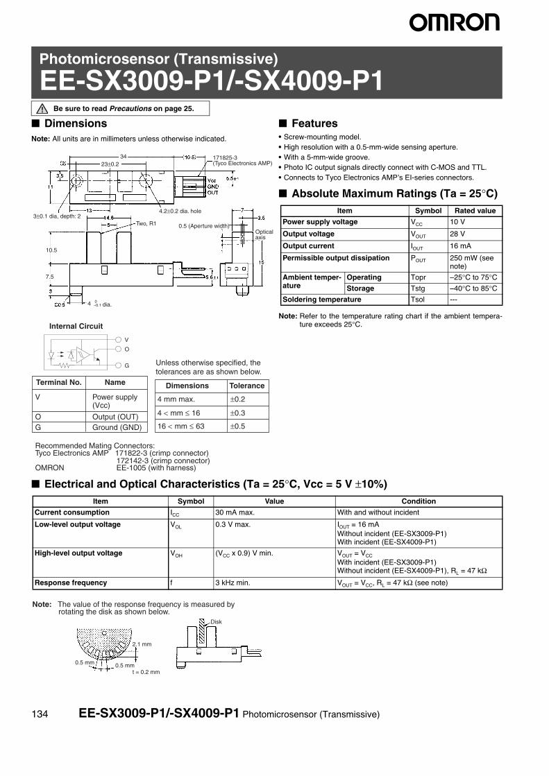
Photomicrosensor (Transmissive)
EE-SX3009-P1/-SX4009-P1Be sure to read Precautions on page 25.
■ DimensionsNote: All units are in millimeters unless otherwise indicated.
■ Features• Screw-mounting model.• High resolution with a 0.5-mm-wide sensing aperture.• With a 5-mm-wide groove.• Photo IC output signals directly connect with C-MOS and TTL.• Connects to Tyco Electronics AMP’s EI-series connectors.
■ Absolute Maximum Ratings (Ta = 25°C)
Note: Refer to the temperature rating chart if the ambient tempera-ture exceeds 25°C.
■ Electrical and Optical Characteristics (Ta = 25°C, Vcc = 5 V ±10%)
Internal Circuit
Dimensions Tolerance
4 mm max. ±0.2
4 < mm ≤ 16 ±0.3
16 < mm ≤ 63 ±0.5
Terminal No. Name
V Power supply (Vcc)
O Output (OUT)G Ground (GND)
V
G
O
Recommended Mating Connectors:Tyco Electronics AMP 171822-3 (crimp connector) 172142-3 (crimp connector)OMRON EE-1005 (with harness)
Optical axis
171825-3(Tyco Electronics AMP)
3±0.1 dia, depth: 2
0.5 (Aperture width)Two, R1
4.2±0.2 dia. hole
4 0−0.1 dia.
3423±0.2
10.5
7.5
Unless otherwise specified, the tolerances are as shown below.
Item Symbol Rated value
Power supply voltage VCC 10 V
Output voltage VOUT 28 V
Output current IOUT 16 mA
Permissible output dissipation POUT 250 mW (see note)
Ambient temper-ature
Operating Topr –25°C to 75°CStorage Tstg –40°C to 85°C
Soldering temperature Tsol ---
Item Symbol Value Condition
Current consumption ICC 30 mA max. With and without incident
Low-level output voltage VOL 0.3 V max. IOUT = 16 mA Without incident (EE-SX3009-P1)With incident (EE-SX4009-P1)
High-level output voltage VOH (VCC x 0.9) V min. VOUT = VCC With incident (EE-SX3009-P1)Without incident (EE-SX4009-P1), RL = 47 kΩ
Response frequency f 3 kHz min. VOUT = VCC, RL = 47 kΩ (see note)
Note: The value of the response frequency is measured by rotating the disk as shown below.
2.1 mm
0.5 mm0.5 mm
t = 0.2 mm
Disk
134 EE-SX3009-P1/-SX4009-P1 Photomicrosensor (Transmissive)

■ Engineering DataNote: The values in the parentheses apply to the EE-SX4009-P1.
Wiring
Output Allowable Dissipation vs. Ambient Temperature Characteristics
Ambient temperature Ta (°C)
Sensing Position Characteristics (Typical)
Out
put a
llow
able
dis
sipa
tion
Pc
(m
W)
Out
put t
rans
isto
rDistance d (mm)
Center of optical axis
Ligh
t int
erru
ptin
g pl
ate
d1 = 0±0.3 mm VCC = 5 V, Ta = 25°CRL = 47 kΩ
ON (OFF)
OFF (ON)
EE-1005 Connector
(1) (2)(3)
1,000±20
No. Name Model Quantity Maker
1 Receptacle housing 171822-3 1 Tyco Elec-tronics AMP
2 Receptacle contact 170262-1 3 Tyco Elec-tronics AMP
3 Lead wire UL1007 AWG24 3 ---
Connector circuit no.
Lead wire color
Output when connected to EE-SX4009-P1/EE-SX3009-P1
1 Red VCC
2 Orange GND
3 Yellow OUT
EE-SX3009-P1/-SX4009-P1 Photomicrosensor (Transmissive) 135

Photomicrosensor (Transmissive)
EE-SX4134Be sure to read Precautions on page 25.
■ DimensionsNote: All units are in millimeters unless otherwise indicated.
■ Features• Ultra-compact model.• Photo IC output model.• Operates at a VCC of 2.2 to 7 V.
• PCB surface mounting type.
■ Absolute Maximum Ratings (Ta = 25°C)
Note: 1. Refer to the temperature rating chart if the ambient temper-ature exceeds 25°C.
2. Complete soldering within 10 seconds for reflow solderingand within 3 seconds for manual soldering.
■ Electrical and Optical Characteristics (Ta = 25°C)
Internal Circuit
Terminal No. NameA Anode
K Cathode
V Supply voltage (Vcc)
O Output (OUT)
G Ground (GND)
A
K
V
G
O
Unless otherwise specified, the tolerances are ±0.15 mm.
Optical axis
Item Symbol Rated value
Emitter Forward current IF 25 mA (see note 1)
Reverse voltage VR 5 V
Detector Supply voltage VCC 9 V
Output voltage VOUT 17 V
Output current IOUT 8 mA
Permissible output dissipation
POUT 80 mW (see note 1)
Ambient temperature
Operating Topr –25°C to 85°CStorage Tstg –40°C to 90°CReflow soldering Tsol 255°C (see note 2)
Manual soldering Tsol 350°C (see note 2)
Item Symbol Value Condition
Emitter Forward voltage VF 1.2 V typ., 1.4 V max. IF = 20 mA
Reverse current IR 0.01 μA typ., 10 μA max. VR = 5 V
Peak emission wave-length
λP 940 nm typ. IF = 20 mA
Detector Power supply voltage VCC 2.2 V min., 7 V max. ---
Low-level output voltage VOL 0.12 V typ., 0.4 V max. Vcc = 2.2 to 7 V, IOL = 8 mA, IF = 7 mA
High-level output current IOH 10 μA max. Vcc = 2.2 to 7 V, IF = 0 mA, VOUT = 17 V
Current consumption ICC 2.8 mA typ., 4 mA max. Vcc = 7 V
Peak spectral sensitivity wavelength
λP 870 mm typ. Vcc = 2.2 to 7 V
LED current when output is ON IFT 2.0 mA typ., 3.5 mA max. VCC = 2.2 to 7 V
Hysteresis ΔH 21% typ. VCC = 2.2 to 7 V (see note 1)
Response frequency f 3 kHz min. VCC = 2.2 to 7 V, IF = 5 mA, IOL = 8 mA (see note 2)
Response delay time tPHL 7 μs typ. VCC = 2.2 to 7 V, IF = 5 mA, IOL = 8 mA (see note 3)
Response delay time tPLH 18 μs typ. VCC = 2.2 to 7 V, IF = 5 mA, IOL = 8 mA (see note 3)
136 EE-SX4134 Photomicrosensor (Transmissive)

■ Engineering Data
2.1 mm
0.5 mm0.5 mm
Disk
Input
Output
Note: 1. Hysteresis denotes the difference in forward LED current value, expressed in percentage, calculated from the respective forward LED currents when the photo IC in turned from ON to OFF and when the photo IC in turned from OFF to ON.
2. The value of the response frequency is measured by rotating the disk as shown below.
3. The following illustrations show the definition of response delay time.
Forward Current vs. Collector Dissipation Temperature Rating
Forward Current vs. Forward Voltage Characteristics (Typical)
LED Current vs. Supply Voltage (Typical)
Forward voltage VF (V)
Low-level Output Voltage vs. Output Current (Typical)
Current Consumption vs. Supply Voltage (Typical)
Response Delay Time vs. Forward Current (Typical)
Repeat Sensing Position Characteristics (Typical)
Out
put t
rans
isto
r
Distance d (mm)
0.01
Supply voltage VCC (V)Lo
w le
vel o
utpu
t vol
tage
VO
L (V
)
Cur
rent
con
sum
ptio
n Ic
c (m
A)
Supply voltage VCC (V) Forward current IF (mA)
VCC = 5 V IF = 7 mA
IOL = 8 mA
IOL = 0.5 mA
Ta = 25°C IF = 0 mA
Ta = 25°C IF = 5 mAVCC = 5 V RL = 4.7 kΩn = repeat 20 times
Ambient temperature Ta (°C)
Out
put a
llow
able
dis
sipa
tion
PC (
mW
)
For
war
d cu
rren
t I F
(m
A)
For
war
d cu
rren
t I F
(m
A)
LED
cur
rent
IF
T (
mA
) Ta = 25°CRL = 4.7 kΩ
Res
pons
e de
lay
time
t PH
L, t P
LH (
μs)
IOL = 8 mAVCC = 5 V Ta = 25°C
LED
cur
rent
IF
T (
mA
)
Ambient temperature Ta (°C)
VCC = 5 VRL = 4.7 kΩ
Ta = −30°C
Ta = 25°C
Ta = 70°C
Low
leve
l out
put v
olta
ge V
OL
(V)
Output current IC (mA)Ambient temperature Ta (°C)
IF = 7 mA
LED Current vs. Ambient Temper-ature Characteristics (Typical)
Low-level Output Voltage vs. Am-bient Temperature Characteristics (Typical)
40
35
30
25
20
15
10
5
00 30205 10 15 25
tPHL
tPLH
INPUT
OUTPUTt
t
tPLHtPHL
IF
VCC
OUT
GND
IF ICC
VOUT
RL VCC = 5 V RL = 4.7 kΩ
Ta = 25°C
EE-SX4134 Photomicrosensor (Transmissive) 137

Unit: mm (inch)
■ Tape and Reel
Reel
Tape
Tape configuration
Tape quantity2,000 pcs./reel
21±0.8 dia.2±0.5
13±0.5 dia.
80±1 dia.
330±2 dia.
12.4 +20
18.4 max.
Product name
Quantity
Lot number
1.5 dia.
Terminating part (40 mm min.)
Pull-out directionEmpty
(40 mm min.)
Parts mounted Leading part (400 mm min.)
138 EE-SX4134 Photomicrosensor (Transmissive)

Precautions
■ Soldering Information
Reflow soldering• The following soldering paste is recommended:
Melting temperature: 216 to 220°CComposition: Sn 3.5 Ag 0.75 Cu
• The recommended thickness of the metal mask for screen printingis between 0.2 and 0.25 mm.
• Set the reflow oven so that the temperature profile shown in the fol-lowing chart is obtained for the upper surface of the product beingsoldered.
Manual soldering• Use”Sn 60” (60% tin and 40% lead) or solder with silver content.• Use a soldering iron of less than 25 W, and keep the temperature
of the iron tip at 300°C or below.• Solder each point for a maximum of three seconds.• After soldering, allow the product to return to room temperature
before handling it.
StorageTo protect the product from the effects of humidity until the package is opened, dry-box storage is recommended. If this is not possible, store the product under the following conditions:
Temperature: 10 to 30°CHumidity: 60% max.
The product is packed in a humidity-proof envelope. Reflow soldering must be done within 48 hours after opening the envelope, during which time the product must be stored under 30°C at 80% maximum humidity.If it is necessary to store the product after opening the envelope, use dry-box storage or reseal the envelope.
BakingIf a product has remained packed in a humidity-proof envelope for six months or more, or if more than 48 hours have lapsed since the envelope was opened, bake the product under the following conditions before use:
Reel: 60°C for 24 hours or moreBulk: 80°C for 4 hours or more
260°C max.
Time
120 sec
Tem
pera
ture
1 to 5°C/s 150 to 180°C
40 sec max.
10 sec max.
1 to 5°C/s 255°C max.
230°C max.
EE-SX4134 Photomicrosensor (Transmissive) 139

Photomicrosensor (Transmissive)
EE-SX4235A-P2Be sure to read Precautions on page 25.
■ DimensionsNote: All units are in millimeters unless otherwise indicated.
■ Features• Snap-in mounting model.• Mounts to 1.0-, 1.2- and 1.6-mm-thick panels.• High resolution with a 0.5-mm-wide sensing aperture.• With a 5-mm-wide slot.• Photo IC output signals directly connect with C-MOS and TTL.• Connects to Tyco Electronics AMP’s CT-series connectors.
■ Absolute Maximum Ratings (Ta = 25°C)
Note: Refer to the temperature rating chart if the ambient tempera-ture exceeds 25°C.
■ Electrical and Optical Characteristics (Ta = 25°C, VCC = 5 V ±10%)
Internal Circuit
Terminal No. Name
V Power supply (Vcc)
O Output (OUT)G Ground (GND)
V
G
O
Recommended Mating Connectors:Tyco Electronics AMP 179228-3 (crimp connector)
175778-3 (crimp connector) 173977-3 (press-fit connector)
Dimensions Tolerance
3 mm max. ±0.3
3 < mm ≤ 6 ±0.375
6 < mm ≤ 10 ±0.45
10 < mm ≤ 18 ±0.55
18 < mm ≤ 30 ±0.65
292250-3 (Tyco Electronics AMP)
0.5 (Aperture width)
3.2 (Aperture width)
Optical axis
7.6±0.2Four, R0.5
(1.2)
Note: The dimension is specified by datum A only.
Unless otherwise specified, the tolerances are as shown below.
(see note)
Item Symbol Rated value
Power supply voltage VCC 7 V
Output voltage VOUT 28 V
Output current IOUT 16 mA
Permissible output dissipation POUT 250 mW (see note)
Ambient temper-ature
Operating Topr –25°C to 75°CStorage Tstg –40°C to 85°C
Soldering temperature Tsol ---
Item Symbol Value Condition
Current consumption ICC 16.5 mA max. With and without incident
Low-level output voltage VOL 0.35 V max. IOUT = 16 mA with incident
High-level output voltage VOH (VCC x 0.9) V min. VOUT = VCC without incident, RL = 47 kΩ
Response frequency f 3 kHz min. VOUT = VCC, RL = 47 kΩ (see note)
Note: The value of the response frequency is measured by rotating the disk as shown below.
2.1 mm
0.5 mm0.5 mm
t = 0.2 mm
Disk
140 EE-SX4235A-P2 Photomicrosensor (Transmissive)

■ Engineering Data
■ Recommended Mounting Holes
• When mounting the Photomicrosensor to a panel with a hole opened by pressing, make sure that the hole has no burrs. The mounting strengthof the Photomicrosensor will decrease if the hole has burrs.
• When mounting the Photomicrosensor to a panel with a hole opened by pressing, be sure to mount the Photomicrosensor on the pressing sideof the panel.
• The mounting strength of the Photomicrosensor will increase if the Photomicrosensor is mounted to a panel with a hole that is only a little largerthan the size of the Photomicrosensor, in which case, however, it will be difficult to mount the Photomicrosensor to the panel. The mountingstrength of the Photomicrosensor will decrease if the Photomicrosensor is mounted to a panel with a hole that is comparatively larger than thesize of the Photomicrosensor, in which case, however, it will be easy to mount the Photomicrosensor to the panel. When mounting the Photomi-crosensor to a panel, open an appropriate hole for the Photomicrosensor according to the application.
• After mounting the Photomicrosensor to any panel, make sure that the Photomicrosensor does not wobble.• When mounting the Photomicrosensor to a molding with a hole, make sure that the edges of the hole are sharp enough, otherwise the Photomi-
crosensor may fall out.
Output Allowable Dissipation vs. Ambient Temperature Characteristics
Ambient temperature Ta (°C)
Sensing Position Characteristics (Typical)
Out
put a
llow
able
dis
sipa
tion
Pc
(m
W)
Out
put t
rans
isto
r
Distance d (mm)
d1 = 0±0.3 mm VCC = 5 V Ta = 25°C RL = 47 kΩ
Center of optical axis
Ligh
t int
erru
ptin
g pl
ate
ON
−3 −2 −1 0 1 2 3
OFF
d2
d
Sensing Position Characteristics (Typical)
Out
put t
rans
isto
r
Distance d (mm)
Cen
ter
of o
ptic
al a
xisd2 = 0±1.3 mm VCC = 5 V
Ta = 25°C RL = 47 kΩ
t = 1.0 mm t = 1.2 mm
t = 1.6 mm
17.1±0.1(for t =1.0,1.2,1.6)
3.7±
0.1
EE-SX4235A-P2 Photomicrosensor (Transmissive) 141

Photomicrosensor (Transmissive)
EE-SX3239-P2Be sure to read Precautions on page 25.
■ DimensionsNote: All units are in millimeters unless otherwise indicated.
■ Features• Snap-in mounting model.• Mounts to 1.0-, 1.2- and 1.6-mm-thick panels.• High resolution with a 0.5-mm-wide sensing aperture.• With a 5-mm-wide slot.• Photo IC output signals directly connect with C-MOS and TTL.• Connects to Tyco Electronics AMP’s CT-series connectors.
■ Absolute Maximum Ratings (Ta = 25°C)
Note: Refer to the temperature rating chart if the ambient tempera-ture exceeds 25°C.
■ Electrical and Optical Characteristics (Ta = 25°C, VCC = 5 V ±10%)
Internal Circuit
Terminal No. Name
V Power supply (Vcc)
O Output (OUT)
G Ground (GND)
V
G
O
Recommended Mating Connectors:Tyco Electronics AMP 175778-3 (crimp connector)
173977-3 (press-fit connector)
Dimensions Tolerance
3 mm max. ±0.3
3 < mm ≤ 6 ±0.375
6 < mm ≤ 10 ±0.45
10 < mm ≤ 18 ±0.55
18 < mm ≤ 30 ±0.65
Post header292250-3 (Tyco Electronics AMP)
(2.4), Aperture width 0.5,
Aperture width
Note: The asterisked dimension is specified by datum A only.
Unless otherwise specified, the tolerances are as shown below.
179228-3 (crimp connector)
Item Symbol Rated value
Power supply voltage VCC 7 V
Output voltage VOUT 28 V
Output current IOUT 16 mA
Permissible output dissipation POUT 250 mW (see note)
Ambient temper-ature
Operating Topr –20°C to 75°CStorage Tstg –40°C to 85°C
Soldering temperature Tsol ---
Item Symbol Value Condition
Current consumption ICC 16.5 mA max. With and without incident
Low-level output voltage VOL 0.35 V max. IOUT = 16 mA without incident (EE-SX3239-P2)
High-level output voltage VOH (VCC x 0.9) V min. VOUT = VCC with incident (EE-SX3239-P2), RL = 47 kΩ
Response frequency f 3 kHz min. VOUT = VCC, RL = 47 kΩ (see note)
Note: The value of the response frequency is measured by rotating the disk as shown below.
2.1 mm
0.5 mm0.5 mm
t = 0.2 mm
Disk
142 EE-SX3239-P2 Photomicrosensor (Transmissive)

■ Engineering Data
■ Recommended Mounting Holes
• When mounting the Photomicrosensor to a panel with a hole opened by pressing, make sure that the hole has no burrs. The mounting strengthof the Photomicrosensor will decrease if the hole has burrs.
• When mounting the Photomicrosensor to a panel with a hole opened by pressing, be sure to mount the Photomicrosensor on the pressing sideof the panel.
• The mounting strength of the Photomicrosensor will increase if the Photomicrosensor is mounted to a panel with a hole that is only a little largerthan the size of the Photomicrosensor, in which case, however, it will be difficult to mount the Photomicrosensor to the panel. The mountingstrength of the Photomicrosensor will decrease if the Photomicrosensor is mounted to a panel with a hole that is comparatively larger than thesize of the Photomicrosensor, in which case, however, it will be easy to mount the Photomicrosensor to the panel. When mounting the Photomi-crosensor to a panel, open an appropriate hole for the Photomicrosensor according to the application.
• After mounting the Photomicrosensor to any panel, make sure that the Photomicrosensor does not wobble.• When mounting the Photomicrosensor to a molding with a hole, make sure that the edges of the hole are sharp enough, otherwise the Photomi-
crosensor may fall out.
Output Allowable Dissipation vs. Ambient Temperature Characteristics
Sensing Position Characteristics (Typical)
Out
put a
llow
able
dis
sipa
tion
Pc
(m
W)
Distance d (mm)
Center of optical axis
Ligh
t int
erru
ptin
g pl
ate
Ambient temperature Ta (°C)
d1 = 0±0.3 mm VCC = 5 V Ta = 25°C RL = 47 kΩ
Sensing Position Characteristics (Typical)
Out
put t
rans
isto
r
Distance d (mm)
Cen
ter
of o
ptic
al a
xis
ON
−3 −2 −1 0 1 2 3
OFF
d2
d
VCC = 5 V Ta = 25°C RL = 47 kΩ
d2 = 0±1.1 mm
Out
put t
rans
isto
r
EE-SX3239-P2 Photomicrosensor (Transmissive) 143

Photomicrosensor (Transmissive)
EE-SX460-P1Be sure to read Precautions on page 25.
■ DimensionsNote: All units are in millimeters unless otherwise indicated.
■ Features• Snap-in mounting model.• Mounts to 0.8- to 1.6-mm-thick panels.• High resolution (aperture width of 0.5 mm)• With a 5-mm-wide slot.• Photo IC output signals directly connect with C-MOS and TTL.• Connects to Tyco Electronics AMP’s EI-series connectors.
■ Absolute Maximum Ratings (Ta = 25°C)
Note: Refer to the temperature rating chart if the ambient tempera-ture exceeds 25°C.
■ Electrical and Optical Characteristics (Ta = 25°C, VCC = 5 V±10%)
Internal Circuit
Terminal No. Name
V Power supply (Vcc)
O Output (OUT)G Ground (GND)
V
G
O
Recommended Mating Connectors:Tyco Electronics AMP 171822-3 (crimp connector) 172142-3 (crimp connector)OMRON EE-1005 (with harness)
Dimensions Tolerance
3 mm max. ±0.3
3 < mm ≤ 6 ±0.375
6 < mm ≤ 10 ±0.45
10 < mm ≤ 18 ±0.55
18 < mm ≤ 30 ±0.65
171826-3(Tyco Electronics AMP)
Optical axis
0.5 (Aperture width)
Optical axis
Two, R1
Mounting face
15±0.2
Unless otherwise specified, the tolerances are as shown below.
Item Symbol Rated value
Power supply voltage VCC 10 V
Output voltage VOUT 28 V
Output current IOUT 16 mA
Permissible output dissipation POUT 250 mW (see note)
Ambient temper-ature
Operating Topr –20°C to 75°CStorage Tstg –40°C to 85°C
Soldering temperature Tsol ---
Item Symbol Value Condition
Current consumption ICC 30 mA max. With and without incident
Low-level output voltage VOL 0.3 V max. IOUT = 16 mA with incident
High-level output voltage VOH (VCC x 0.9) V min. VOUT = VCC without incident, RL = 47 kΩ
Response frequency f 3 kHz min. VOUT = VCC, RL = 47 kΩ (see note)
Note: The value of the response frequency is measured by rotating the disk as shown below.
Disk
2.1 mm
t = 0.2 mm0.5 mm0.5 mm
144 EE-SX460-P1 Photomicrosensor (Transmissive)

■ Engineering Data
Wiring
■ Recommended Mounting Hole Dimensions and Mounting and Dismounting Method
The Photomicrosensor can be mounted to 0.8- to 1.6-mm-thick panels.Refer to the above mounting hole dimensions and open the mounting holes in the panel to which the Photomicrosensor will be mounted.Insert into the holes the Photomicrosensor’s mounting portions with a force of three to five kilograms but do not press in the Photomicrosensor at one time. The Photomicrosensor can be easily mounted by inserting the mounting portions halfway and then slowly pressing the Photomicrosensor onto the panel.There are two ways to dismount the Photomicrosensor. Refer to the following.
Dismounting with ScrewdriverPress the mounting hooks of the Photomicrosensor with a flat-blade screwdriver as shown in the following illustration and pull up the Photomicrosensor.
Dismounting by HandSqueeze the mounting tabs as shown in the following illustration and press the mounting tabs upwards.
Pressed mounting holes are ideal for mounting the Photomicrosensor. When mounting the Photomicrosensor to a panel that has pressed mounting holes for the Photomicrosensor, be sure to mount the Photomicrosensor on the pressing side of the panel, otherwise it may be difficult to mount the Photomicrosensor and an insertion force of five to six kilograms may be required.When mounting the Photomicrosensor to a panel that has mounting holes opened by pressing, make sure that the mounting holes have no burrs, otherwise the lock mechanism of the Photomicrosensor will not work perfectly. After mounting the Photomicrosensor to a panel, be sure to check if the lock mechanism is working perfectly.
Output Allowable Dissipation vs. Ambient Temperature Characteristics
Ambient temperature Ta (°C)
Sensing Position Characteristics (Typical)
Out
put a
llow
able
dis
sipa
tion
Pc
(m
W)
Out
put t
rans
isto
rDistance d (mm)
d1 = 0±0.3 mm VCC = 5 V Ta = 25°C RL = 47 kΩ
Center of optical axis
Ligh
t int
erru
ptin
g pl
ate
EE-1005 Connector
(1) (2) (3)
1,000±20
Sensing Position Characteristics (Typical)
Out
put t
rans
isto
r
Distance d (mm)
Cen
ter
of o
ptic
al a
xis
ON
−3 −2 −1 0 1 2 3
OFF
d2
dVCC = 5 V Ta = 25°C RL = 47 kΩ
d2 = 0±1.1 mm
No. Name Model Quantity Maker
1 Receptacle housing
171822-3 1 Tyco Electronics AMP
2 Receptacle contact
170262-1 3 Tyco Electronics AMP
3 Lead wire UL1007 AWG24 3 ---
Connector circuit no.
Lead wire color Output when connected to EE-SX460-P1
1 Red VCC
2 Orange OUT
3 Yellow GND
Center of sensing slot
Optical axis
Sensor edge Sensor edge on connector side
Flat-blade screwdriver
Mounting hook Panel
Flat-blade screwdriver
Mounting hook
EE-SX460-P1
(1)
(2)
(1)
(2)
Panel (1)(1)
EE-SX460-P1
(2)
PanelThis tapered portion must be on the lower side of the panel, otherwise the Photomicrosensor will not be locked in.
Mounting tab
EE-SX460-P1
EE-SX460-P1 Photomicrosensor (Transmissive) 145

Photomicrosensor (Transmissive)
EE-SX461-P11Be sure to read Precautions on page 25.
■ DimensionsNote: All units are in millimeters unless otherwise indicated.
■ Features• Snap-in-mounting model.• Mounts to 0.8- to 1.6-mm-thick panels.• With a 15-mm-wide slot.• Photo IC output signals directly connect with C-MOS and TTL.• Connects to Tyco Electronics AMP’s EI-series connectors.
■ Absolute Maximum Ratings (Ta = 25°C)
Note: Refer to the temperature rating chart if the ambient tempera-ture exceeds 25°C.
■ Electrical and Optical Characteristics (Ta = 25°C, VCC = 5 V±10%)
Internal Circuit
Terminal No. Name
V Power supply (Vcc)
O Output (OUT)G Ground (GND)
V
G
O
Recommended Mating Connectors:Tyco Electronics AMP 171822-3 (crimp connector) 172142-3 (crimp connector)OMRON EE-1005 (with harness)
Dimensions Tolerance
3 mm max. ±0.3
3 < mm ≤ 6 ±0.375
6 < mm ≤ 10 ±0.45
10 < mm ≤ 18 ±0.55
18 < mm ≤ 30 ±0.65
171826-3 (Tyco Electronics AMP)
2 (Aperture width)
Optical axisTwo, R1
(15)
Unless otherwise specified, the tolerances are as shown below.
Item Symbol Rated value
Power supply voltage VCC 7 V
Output voltage VOUT 28 V
Output current IOUT 16 mA
Permissible output dissipation POUT 250 mW (see note)
Ambient temper-ature
Operating Topr –20°C to 75°CStorage Tstg –40°C to 85°C
Soldering temperature Tsol ---
Item Symbol Value Condition
Current consumption ICC 35 mA max. With and without incident
Low-level output voltage VOL 0.3 V max. IOUT = 16 mA with incident
High-level output voltage VOH (VCC x 0.9) V min. VOUT = VCC without incident, RL = 47 kΩ
Response frequency f 3 kHz min. VOUT = VCC, RL = 47 kΩ (see note)
Note: The value of the response frequency is measured by rotating the disk as shown below.
2.1 mm
t = 0.2 mm0.5 mm0.5 mm
Disk
146 EE-SX461-P11 Photomicrosensor (Transmissive)

■ Engineering Data
Wiring
■ Recommended Mounting Hole Dimensions and Mounting and Dismounting Method
The Photomicrosensor can be mounted to 0.8- to 1.6-mm-thick panels.Refer to the above mounting hole dimensions and open the mounting holes in the panel to which the Photomicrosensor will be mounted.Insert into the holes the Photomicrosensor’s mounting portions with a force of three to five kilograms but do not press in the Photomicrosensor at one time. The Photomicrosensor can be easily mounted by inserting the mounting portions halfway and then slowly pressing the Photomicrosensor onto the panel.There are two ways to dismount the Photomicrosensor. Refer to the following.
Dismounting with ScrewdriverPress the mounting hooks of the Photomicrosensor with a flat-blade screwdriver as shown in the following illustration and pull up the Photomicrosensor.
Dismounting by HandSqueeze the mounting tabs as shown in the following illustration and press the mounting tabs upwards.
Pressed mounting holes are ideal for mounting the Photomicrosensor. When mounting the Photomicrosensor to a panel that has pressed mounting holes for the Photomicrosensor, be sure to mount the Photomicrosensor on the pressing side of the panel, otherwise it may be difficult to mount the Photomicrosensor and an insertion force of five to six kilograms may be required.When mounting the Photomicrosensor to a panel that has mounting holes opened by pressing, make sure that the mounting holes have no burrs, otherwise the lock mechanism of the Photomicrosensor will not work perfectly. After mounting the Photomicrosensor to a panel, be sure to check if the lock mechanism is working perfectly.
Output Allowable Dissipation vs. Ambient Temperature Characteristics
Sensing Position Characteristics (Typical)
Distance d (mm)EE-1005 Connector
(1) (2) (3)
Center of optical axis
Ligh
t int
erru
ptin
g pl
ate
Ambient temperature Ta (°C)Out
put a
llow
able
dis
sipa
tion
Pc
(m
W)
d1 = 0±1.1 mm VCC = 5 V Ta = 25°C RL = 47 kΩ
1,000±20
Sensing Position Characteristics (Typical)
Out
put t
rans
isto
r
Distance d (mm)
Cen
ter
of o
ptic
al a
xis
ON
−3 −2 −1 0 1 2 3
OFF
d2
dVCC = 5 V Ta = 25°C RL = 47 kΩ
d2 = 0±1.1 mm
Out
put t
rans
isto
r
No. Name Model Quantity Maker
1 Receptacle housing
171822-3 1 Tyco Electronics AMP
2 Receptacle contact
170262-1 3 Tyco Electronics AMP
3 Lead wire UL1007 AWG24 3 ---
Connector circuit no.
Lead wire color Output when connected to EE-SX461-P11
1 Red VCC
2 Orange OUT
3 Yellow GND
Optical axis
Sensor edgeCenter of sensing slot
Sensor edge (to post header)
Flat-blade screwdriver
Mounting hook Panel Mounting hook
Flat-blade screwdriver
EE-SX461-P11
(1)
(2)
(1)
(2)
Panel (1) (1)
EE-SX461-P11
(2)
Panel
Mounting tab
This tapered portion must be on the lower side of the panel, otherwise the Photomicrosensor will not be locked in.
EE-SX461-P11
EE-SX461-P11 Photomicrosensor (Transmissive) 147

Photomicrosensor (Actuator Mounted)
EE-SA407-P2Be sure to read Precautions on page 25.
■ DimensionsNote: All units are in millimeters unless otherwise indicated.
■ Features• An actuator can be attached.• Snap-in mounting model.• Mounts to 1.0-, 1.2- and 1.6-mm-thick panels.• High resolution with a 0.5-mm-wide sensing aperture.• With a 3.6-mm-wide slot.• Photo IC output signals directly connect with logic circuit and TTL.• Connects to Tyco Electronics AMP’s CT-series connectors.
■ Absolute Maximum Ratings (Ta = 25°C)
Note: Refer to the temperature rating chart if the ambient tempera-ture exceeds 25°C.
■ Electrical and Optical Characteristics (Ta = 25°C, VCC = 5 V ±10%)
Internal Circuit
Terminal No. Name
V Power supply (Vcc)
O Output (OUT)G Ground (GND)
V
G
0
Recommended Mating Connectors:Tyco Electronics AMP 179228-3 (crimp connector)
175778-3 (crimp connector) 173977-3 (press-fit connector)
Dimensions Tolerance
3 mm max. ±0.3
3 < mm ≤ 6 ±0.375
6 < mm ≤ 10 ±0.45
10 < mm ≤ 18 ±0.55
18 < mm ≤ 30 ±0.65
0.5 (Aperture width)
Optical axis
2.2+0.1 0 dia.
292250-3(Tyco Electronics AMP)
(see note)
Note: The dimension is specified by datum A only.
Unless otherwise specified, the tolerances are as shown below.
▲▲
Item Symbol Rated value
Power supply voltage VCC 7 V
Output voltage VOUT 28 V
Output current IOUT 16 mA
Permissible output dissipation POUT 250 mW (see note)
Ambient temper-ature
Operating Topr –20°C to 75°CStorage Tstg –40°C to 85°C
Soldering temperature Tsol ---
Item Symbol Value Condition
Current consumption ICC 30 mA max. With and without incident
Low-level output voltage VOL 0.35 V max. IOUT = 16 mA with incident
High-level output voltage VOH (VCC x 0.9) V min. VOUT = VCC without incident, RL = 47 kΩ
Response frequency f 3 kHz min. VOUT = VCC, RL = 47 kΩ (see note)
Note: The value of the response frequency is measured by rotating the disk as shown below.
2.1 mm
0.5 mm0.5 mm
t = 0.2 mm
Disk
148 EE-SA407-P2 Photomicrosensor (Actuator Mounted)

■ Engineering Data
■ Recommended Mounting Holes
• When mounting the Photomicrosensor to a panel with a hole opened by pressing, make sure that the hole has no burrs. The mounting strengthof the Photomicrosensor will decrease if the hole has burrs.
• When mounting the Photomicrosensor to a panel with a hole opened by pressing, be sure to mount the Photomicrosensor on the pressing sideof the panel.
• The mounting strength of the Photomicrosensor will increase if the Photomicrosensor is mounted to a panel with a hole that is only a little largerthan the size of the Photomicrosensor, in which case, however, it will be difficult to mount the Photomicrosensor to the panel. The mountingstrength of the Photomicrosensor will decrease if the Photomicrosensor is mounted to a panel with a hole that is comparatively larger than thesize of the Photomicrosensor, in which case, however, it will be easy to mount the Photomicrosensor to the panel. When mounting the Photomi-crosensor to a panel, open an appropriate hole for the Photomicrosensor according to the application.
• After mounting the Photomicrosensor to any panel, make sure that the Photomicrosensor does not wobble.• When mounting the Photomicrosensor to a molding with a hole, make sure that the edges of the hole are sharp enough, otherwise the Photomi-
crosensor may come fall out.
Output Allowable Dissipation vs. Ambient Temperature Characteristics
Sensing Position Characteristics (Typical)
Out
put a
llow
able
dis
sipa
tion
Pc
(m
W)
Out
put t
rans
isto
rDistance d (mm)
Center of optical axis
Ligh
t int
erru
ptin
g pl
ate
Ambient temperature Ta (°C)
d1 = 0±0.3 mm VCC = 5 V Ta = 25°C RL = 47 kΩ
Sensing Position Characteristics (Typical)
Out
put t
rans
isto
r
Distance d (mm)
Cen
ter
of o
ptic
al a
xis
ON
−3 −2 −1 0 1 2 3
OFF
d2
dVCC = 5 V Ta = 25°C RL = 47 kΩ
d2 = 0±1.1 mm
t = 1.0 mm t = 1.2 mm
t = 1.6 mm
17.1±0.1(for t =1.0,1.2,1.6)
Actuator Dimensions 3
0−0.2dia.
2±0.1 dia.
Note: 1. Make sure that the portions marked with dotted lines have no burrs.
2. The material of the actuator must be selected by considering the infrared permeability of the actuator.
EE-SA407-P2 Photomicrosensor (Actuator Mounted) 149

Photomicrosensor (Reflective)
EE-SY110Be sure to read Precautions on page 25.
■ DimensionsNote: All units are in millimeters unless otherwise indicated.
■ Features• Compact reflective model with a molded housing.
■ Absolute Maximum Ratings (Ta = 25°C)
Note: 1. Refer to the temperature rating chart if the ambient temper-ature exceeds 25°C.
2. The pulse width is 10 μs maximum with a frequency of100 Hz.
3. Complete soldering within 10 seconds.
■ Electrical and Optical Characteristics (Ta = 25°C)
Note: The letter “d” indicates the distance between the top surface of the sensor and the sensing object.
Internal Circuit
Terminal No. Name
A Anode
K Cathode
C CollectorE Emitter
Dimensions Tolerance
3 mm max. ±0.2
3 < mm ≤ 6 ±0.24
6 < mm ≤ 10 ±0.29
10 < mm ≤ 18 ±0.35
18 < mm ≤ 30 ±0.42
Four, R1.5
Four, 0.25
Four, 0.5
15 to 18
15.2±0.2
A
K
C
E
Unless otherwise specified, the tolerances are as shown below.
Item Symbol Rated value
Emitter Forward current IF 50 mA (see note 1)
Pulse forward cur-rent
IFP 1 A (see note 2)
Reverse voltage VR 4 V
Detector Collector–Emitter voltage
VCEO 30 V
Emitter–Collector voltage
VECO ---
Collector current IC 20 mA
Collector dissipa-tion
PC 100 mW (see note 1)
Ambient tem-perature
Operating Topr –40°C to 85°CStorage Tstg –40°C to 85°C
Soldering temperature Tsol 260°C(see note 3)
Item Symbol Value Condition
Emitter Forward voltage VF 1.2 V typ., 1.5 V max. IF = 30 mA
Reverse current IR 0.01 μA typ., 10 μA max. VR = 4 V
Peak emission wavelength λP 940 nm typ. IF = 20 mA
Detector Light current IL 200 μA min., 2,000 μA max. IF = 20 mA, VCE = 10 VWhite paper with a reflection ratio of 90%, d = 5 mm (see note)
Dark current ID 2 nA typ., 200 nA max. VCE = 10 V, 0 lx
Leakage current ILEAK 2 μA max. IF = 20 mA, VCE = 10 V with no reflec-tion
Collector–Emitter saturated volt-age
VCE (sat) --- ---
Peak spectral sensitivity wave-length
λP 850 nm typ. VCE = 10 V
Rising time tr 30 μs typ. VCC = 5 V, RL = 1 kΩ, IL = 1 mA
Falling time tf 30 μs typ. VCC = 5 V, RL = 1 kΩ, IL = 1 mA
150 EE-SY110 Photomicrosensor (Reflective)

■ Engineering Data
VCE = 10 VIF = 20 mAd = 5 mmSensing object: White paper with a reflection factor of 90%
d
Forward Current vs. Collector Dissipation Temperature Rating
Light Current vs. Forward Current Characteristics (Typical)
Ambient temperature Ta (°C)
Col
lect
or d
issi
patio
n P
c (m
W)
For
war
d cu
rren
t I F
(m
A)
Forward current IF (mA)
Ligh
t cur
rent
IL
(mA
)
Light Current vs. Collector−Emitter Voltage Characteristics (Typical)
Relative Light Current vs. Ambient Temperature Characteristics (Typical)
Dark Current vs. Ambient Temperature Characteristics (Typical)
Collector−Emitter voltage VCE (V)
Ligh
t cur
rent
IL
(mA
)Ambient temperature Ta (°C) Ambient temperature Ta (°C)
Response Time vs. Load Resistance Characteristics (Typical)
Sensing Distance Characteristics (Typical)
Response Time Measurement Circuit
Load resistance RL (kΩ)
Distance d2 (mm)
Sensing Angle Characteristics (Typical)
Angle deviation θ (°)
Input
Output
Input
Output
90 %10 %
0 xIF = 20 mA VCE = 5 V
Vcc = 5 V Ta = 25°C
Ta = 25°Cd = 5 mm
Sensing object: White paper with a reflection factor of 90%
IF = 20 mA
IF = 10 mA
IF = 30 mA
IF = 40 mA
Distance d (mm)
Sensing Position Characteristics (Typical)
Sensing object: White paper with a reflection factor of 90%
Ta = 25°CIF = 20 mAVCE = 10 V
Sensing object: White paper with a reflection factor of 90%
Direction
IF = 20 mAVCE = 10 VTa = 25°Cd1 = 5 mm
Rel
ativ
e lig
ht c
urre
nt I
L (%
)
Dar
k cu
rren
t I D
(nA
)
Res
pons
e tim
e tr,
tf (
μs)
Rel
ativ
e lig
ht c
urre
nt I
L (%
)
Rel
ativ
e lig
ht c
urre
nt I
L (%
)
Ligh
t cur
rent
IL
(μA
)
d = 5 mm VCE = 10 V
VCE = 10 V
EE-SY110 Photomicrosensor (Reflective) 151

Photomicrosensor (Reflective)
EE-SY113Be sure to read Precautions on page 25.
■ DimensionsNote: All units are in millimeters unless otherwise indicated.
■ Features• Compact reflective Photomicrosensor (EE-SY110) with a molded
housing and a dust-tight cover.
■ Absolute Maximum Ratings (Ta = 25°C)
Note: 1. Refer to the temperature rating chart if the ambient temper-ature exceeds 25°C.
2. The pulse width is 10 μs maximum with a frequency of100 Hz.
3. Complete soldering within 10 seconds.
■ Electrical and Optical Characteristics (Ta = 25°C)
Note: The letter “d” indicates the distance between the top surface of the sensor and the sensing object.
Internal Circuit
Terminal No. Name
A Anode
K CathodeC Collector
E Emitter
Dimensions Tolerance
3 mm max. ±0.3
3 < mm ≤ 6 ±0.375
6 < mm ≤ 10 ±0.45
10 < mm ≤ 18 ±0.55
18 < mm ≤ 30 ±0.65
A
K
C
E
Four, 0.5
Four, 0.25
15 to 18
Notch for directional discrimination
Unless otherwise specified, the tolerances are as shown below.
2.5
Item Symbol Rated value
Emitter Forward current IF 50 mA (see note 1)
Pulse forward cur-rent
IFP 1 A (see note 2)
Reverse voltage VR 4 V
Detector Collector–Emitter voltage
VCEO 30 V
Emitter–Collector voltage
VECO ---
Collector current IC 20 mA
Collector dissipa-tion
PC 100 mW (see note 1)
Ambient tem-perature
Operating Topr –40°C to 80°CStorage Tstg –40°C to 85°C
Soldering temperature Tsol 260°C(see note 3)
Item Symbol Value Condition
Emitter Forward voltage VF 1.2 V typ., 1.5 V max. IF = 30 mA
Reverse current IR 0.01 μA typ., 10 μA max. VR = 4 V
Peak emission wavelength λP 940 nm typ. IF = 20 mA
Detector Light current IL 160 μA min., 1,600 μA max. IF = 20 mA, VCE = 10 VWhite paper with a reflection ratio of 90%, d = 4.4 mm (see note)
Dark current ID 2 nA typ., 200 nA max. VCE = 10 V, 0 lx
Leakage current ILEAK 2 μA max. IF = 20 mA, VCE = 10 V with no reflec-tion
Collector–Emitter saturated volt-age
VCE (sat) --- ---
Peak spectral sensitivity wave-length
λP 850 nm typ. VCE = 10 V
Rising time tr 30 μs typ. VCC = 5 V, RL = 1 kΩ, IL = 1 mA
Falling time tf 30 μs typ. VCC = 5 V, RL = 1 kΩ, IL = 1 mA
152 EE-SY113 Photomicrosensor (Reflective)

■ Engineering Data
Forward Current vs. Collector Dissipation Temperature Rating
Light Current vs. Forward Current Characteristics (Typical)
Light Current vs. Collector−Emitter Voltage Characteristics (Typical)
Relative Light Current vs. Ambient Temperature Characteristics (Typical)
Dark Current vs. Ambient Temperature Characteristics (Typical)
Response Time vs. Load Resistance Characteristics (Typical)
Sensing Distance Characteristics (Typical)
Response Time Measurement Circuit
Distance d2 (mm)
Sensing Angle Characteristics (Typical)
Input
Output
Input
Output
90 %10 %
Distance d (mm)
Sensing Position Characteristics (Typical)
Ta = 25°CVCE = 10 VIF = 20 mAd = 4.4 mmSensing object: White paper with a reflection factor of 90% Direction
Sensing object: White paper with a reflection factor of 90%
Sensing object: White paper with a reflection factor of 90%
d = 4.4 mmSensing object: White paper with a reflection factor of 90%
Sensing object: White paper with a reflection factor of 90%
d1
d2
Ambient temperature Ta (°C)
Col
lect
or d
issi
patio
n P
c (m
W)
For
war
d cu
rren
t I F
(m
A)
Forward current IF (mA)
Ligh
t cur
rent
IL
(μA
)
Collector−Emitter voltage VCE (V)
Ligh
t cur
rent
IL
(mA
)
Ambient temperature Ta (°C) Ambient temperature Ta (°C) Load resistance RL (kΩ)
Angle deviation θ (°)
0 xIF = 20 mA VCE = 5 V
Vcc = 5 V Ta = 25°C
IF = 20 mA
IF = 10 mA
IF = 30 mA
IF = 40 mA
Ta = 25°CIF = 20 mAVCE = 10 V
IF = 20 mAVCE = 10 VTa = 25°Cd1 = 4.4 mm
Rel
ativ
e lig
ht c
urre
nt I
L (%
)
Dar
k cu
rren
t I D
(nA
)
Res
pons
e tim
e tr,
tf (
μs)
Rel
ativ
e lig
ht c
urre
nt I
L (%
)
Rel
ativ
e lig
ht c
urre
nt I
L (%
)
Ligh
t cur
rent
IL
(μA
)
d = 4.4 mm VCE = 10 V
VCE = 10 V
EE-SY113 Photomicrosensor (Reflective) 153

Photomicrosensor (Reflective)
EE-SY169Be sure to read Precautions on page 25.
■ DimensionsNote: All units are in millimeters unless otherwise indicated.
■ Features• High-quality model with plastic lenses.• Highly precise sensing range with a tolerance of ±0.6 mm horizon-
tally and vertically.• With a red LED sensing dyestuff-type inks.• Limited reflective model.• For lesser LED forward current the EE-SY169B would be a better
choice.
■ Absolute Maximum Ratings (Ta = 25°C)
Note: 1. Refer to the temperature rating chart if the ambient temper-ature exceeds 25°C.
2. The pulse width is 10 μs maximum with a frequency of100 Hz.
3. Complete soldering within 10 seconds.
■ Electrical and Optical Characteristics (Ta = 25°C)
Note: The letter “d” indicates the distance between the top surface of the sensor and the sensing object.
Internal Circuit
Terminal No. Name
A Anode
K CathodeC Collector
E Emitter
Dimensions Tolerance
3 mm max. ±0.3
3 < mm ≤ 6 ±0.375
6 < mm ≤ 10 ±0.45
10 < mm ≤ 18 ±0.55
18 < mm ≤ 30 ±0.65
A
K
C
E
Two, C0.21±0.1 dia.1±0.1 dia.
(see note)
(see note)
Surface A
Unless otherwise specified, the tolerances are as shown below.
Note: These dimensions are for the surface A. Other lead wire pitch dimensions are for the housing surface.
Item Symbol Rated value
Emitter Forward current IF 40 mA (see note 1)
Pulse forward cur-rent
IFP 300 mA (see note 2)
Reverse voltage VR 3 V
Detector Collector–Emitter voltage
VCEO 30 V
Emitter–Collector voltage
VECO ---
Collector current IC 20 mA
Collector dissipa-tion
PC 100 mW (see note 1)
Ambient tem-perature
Operating Topr 0°C to 70°CStorage Tstg –20°C to 80°C
Soldering temperature Tsol 260°C(see note 3)
Item Symbol Value Condition
Emitter Forward voltage VF 1.85 V typ., 2.3 V max. IF = 20 mA
Reverse current IR 0.01 μA typ., 10 μA max. VR = 3 V
Peak emission wavelength λP 660 nm typ. IF = 20 mA
Detector Light current IL 160 μA min., 2,000 μA max. IF = 20 mA, VCE = 5 VWhite paper with a reflection ratio of 90%, d = 4 mm (see note)
Dark current ID 2 nA typ., 200 nA max. VCE = 5 V, 0 lx
Leakage current ILEAK 2 μA max. IF = 20 mA, VCE = 5 V with no reflection
Collector–Emitter saturated voltage
VCE (sat) --- ---
Peak spectral sensitivity wave-length
λP 850 nm typ. VCE = 5 V
Rising time tr 30 μs typ. VCC = 5 V, RL = 1 kΩ, IL = 1 mA
Falling time tf 30 μs typ. VCC = 5 V, RL = 1 kΩ, IL = 1 mA
154 EE-SY169 Photomicrosensor (Reflective)

■ Engineering Data
Forward Current vs. Collector Dissipation Temperature Rating
Light Current vs. Forward Current Characteristics (Typical)
Light Current vs. Collector−Emitter Voltage Characteristics (Typical)
Relative Light Current vs. Ambient Temperature Characteristics (Typical)
Dark Current vs. Ambient Temperature Characteristics (Typical)
Response Time vs. Load Resistance Characteristics (Typical)
Sensing Distance Characteristics (Typical)
Response Time Measurement Circuit
Load resistance RL (kΩ)
Distance d2 (mm)
Sensing Angle Characteristics (Typical)
Angle deviation θ (°)
Input
Output
Input
Output
90 %10 %
VCE = 10 V0lx
Vcc = 5 V
Distance d (mm)
Sensing Position Characteristics (Typical)
Dar
k C
urre
nt I D
(nA
)
d = 4 mmSensing object: White paper with a reflection factor of 90%
IF = 40 mA
IF = 30 mA
IF = 20 mA
IF = 10 mA
IF = 5 mA
d = 4 mm
Sensing object: White paper with a reflection factor of 90%
Ta = 25°C
Sen-sor
Direction
Sensing object: White paper with a reflection factor of 90%
d = 0
IF = 20 mAVCE = 5 VTa = 25°C d1 = 4 mm
Sensing object
Sensing object: White paper with a reflection factor of 90%
d1 = 3.5 mm d1 = 4.0 mm d1 = 4.5 mm
Direction
Sen-sor
Distance d2 (mm)
Sensing Position Characteristics (Typical)
d = 3 mm d = 4 mm d = 5 mm
Sensing object: White paper with a reflection factor of 90%
d = 3 mm d = 4 mm d = 5 mm
Ta = 25°IF = 20 mA VCE= 10 VSensing object: White paper with a reflection factor of 90%
Sensing Angle Characteristics (Typical)
Angle deviation θ (°)
VCE = 5 V
Ta = 25°C
IF = 20 mAVCE = 10 V
Ambient temperature Ta (°C)
Col
lect
or d
issi
patio
n P
c (m
W)
For
war
d cu
rren
t I F
(m
A)
Forward current IF (mA)
Ligh
t cur
rent
IL
(μA
)
Collector−Emitter voltage VCE (V)
Ligh
t cur
rent
IL
(μA
)Ambient temperature Ta (°C)
IF = 20 mA VCE = 5 V
Rel
ativ
e lig
ht c
urre
nt I
L (%
)
Ambient temperature Ta (°C)
Rel
ativ
e lig
ht c
urre
nt I
L (%
)
Res
pons
e tim
e tr,
tf (
μs)
Rel
ativ
e lig
ht c
urre
nt I
L (%
)
Ta = 25°CIF = 20 mAVCE = 10 V
Rel
ativ
e lig
ht c
urre
nt I
L (%
)
Ligh
t cur
rent
IL
(μA
) Ta = 25°C
IF = 20 mAVCE = 5 V
Rel
ativ
e lig
ht c
urre
nt I
L (%
)
Ta = 25°C
EE-SY169 Photomicrosensor (Reflective) 155

Photomicrosensor (Reflective)
EE-SY169ABe sure to read Precautions on page 25.
■ DimensionsNote: All units are in millimeters unless otherwise indicated.
■ Features• High-quality model with plastic lenses.• Highly precise sensing range with a tolerance of ±0.6 mm horizon-
tally and vertically.• Convergent reflective model with infrared LED.
■ Absolute Maximum Ratings (Ta = 25°C)
Note: 1. Refer to the temperature rating chart if the ambient temper-ature exceeds 25°C.
2. The pulse width is 10 μs maximum with a frequency of100 Hz.
3. Complete soldering within 10 seconds.
■ Electrical and Optical Characteristics (Ta = 25°C)
Note: The letter “d” indicates the distance between the top surface of the sensor and the sensing object.
Internal Circuit
Terminal No. Name
A Anode
K Cathode
C Collector
E Emitter
Dimensions Tolerance
3 mm max. ±0.3
3 < mm ≤ 6 ±0.375
6 < mm ≤ 10 ±0.45
10 < mm ≤ 18 ±0.55
18 < mm ≤ 30 ±0.65
A
K
C
E
Two, C0.21±0.1 dia.1±0.1 dia.
(see note)
(see note)
Surface A
Note: These dimensions are for the surface A. Other lead wire pitch dimensions are for the housing surface.
Unless otherwise specified, the tolerances are as shown below.
Item Symbol Rated value
Emitter Forward current IF 50 mA (see note 1)
Pulse forward cur-rent
IFP 1 A (see note 2)
Reverse voltage VR 3 V
Detector Collector–Emitter voltage
VCEO 30 V
Emitter–Collector voltage
VECO ---
Collector current IC 20 mA
Collector dissipa-tion
PC 100 mW (see note 1)
Ambient tem-perature
Operating Topr 0°C to 70°CStorage Tstg –20°C to 80°C
Soldering temperature Tsol 260°C(see note 3)
Item Symbol Value Condition
Emitter Forward voltage VF 1.5 V max. IF = 30 mA
Reverse current IR 10 μA max. VR = 4 V
Peak emission wavelength λP 920 nm typ. IF = 20 mA
Detector Light current IL 160 μA min., 2,000 μA max. IF = 20 mA, VCE = 5 VWhite paper with a reflection ratio of 90%, d = 4 mm (see note)
Dark current ID 2 nA typ., 200 nA max. VCE = 5 V, 0 lx
Leakage current ILEAK 2 μA max. IF = 20 mA, VCE = 5 V with no reflec-tion
Collector–Emitter saturated volt-age
VCE (sat) --- ---
Peak spectral sensitivity wave-length
λP 850 nm typ. VCE = 5 V
Rising time tr 30 μs typ. VCC = 5 V, RL = 1 kΩ, IL = 1 mA
Falling time tf 30 μs typ. VCC = 5 V, RL = 1 kΩ, IL = 1 mA
156 EE-SY169A Photomicrosensor (Reflective)

■ Engineering Data
Forward Current vs. Collector Dissipation Temperature Rating
Light Current vs. Forward Current Characteristics (Typical)
Light Current vs. Collector−Emitter Voltage Characteristics (Typical)
Relative Light Current vs. Ambient Temperature Characteristics (Typical)
Dark Current vs. Ambient Temperature Characteristics (Typical)
Response Time vs. Load Resistance Characteristics (Typical)
Sensing Distance Characteristics (Typical)
Response Time Measurement Circuit
Sensing Angle Characteristics (Typical)
Input
Output
Input
Output
90 %10 %
Vcc = 5 V Ta = 25°C
Distance d (mm)
Sensing Position Characteristics (Typical)
Sensing Position Characteristics (Typical)
d = 3 mm d = 4 mm d = 5 mm
Sensing Angle Characteristics (Typical)
IF = 20 mA VCE = 5 V Ta = 25°C
Sensing object: White paper with a reflection factor of 90%
d1 = 3.5 mm d1 = 4.0 mm d1 = 4.5 mm
Sensing object: White paper with a reflection factor of 90%
d = 0
d = 3 mm d = 4 mm d = 5 mm
Sensing object: White paper with a reflection factor of 90%
Load resistance RL (kΩ)
Distance d2 (mm)
Angle deviation θ (°)
VCE = 10 V0lx
Dar
k C
urre
nt I D
(nA
)
d = 4 mmSensing object: White paper with a reflection factor of 90%
IF = 40 mA
IF = 30 mA
IF = 20 mA
IF = 10 mA
IF = 5 mA
d = 4 mm
Ta = 25°C
Sen-sor
Direction
IF = 20 mAVCE = 5 VTa = 25°C d1 = 4 mm
Sensing object
DirectionSen-sor
Distance d2 (mm)
Ta = 25°IF = 20 mA VCE= 10 V
Angle deviation θ (°)
VCE = 5 V
Ta = 25°C
IF = 20 mAVCE = 10 V
Ambient temperature Ta (°C)
Col
lect
or d
issi
patio
n P
c (m
W)
For
war
d cu
rren
t I F
(m
A)
Forward current IF (mA)
Ligh
t cur
rent
IL
(μA
)
Collector−Emitter voltage VCE (V)
Ligh
t cur
rent
IL
(μA
)Ambient temperature Ta (°C)
IF = 20 mA VCE = 5 V
Rel
ativ
e lig
ht c
urre
nt I
L (%
)
Ambient temperature Ta (°C)
Rel
ativ
e lig
ht c
urre
nt I
L (%
)
Res
pons
e tim
e tr,
tf (
μs)
Rel
ativ
e lig
ht c
urre
nt I
L (%
)
Ta = 25°CIF = 20 mAVCE = 10 V
Rel
ativ
e lig
ht c
urre
nt I
L (%
)
Ligh
t cur
rent
IL
(μA
)
Rel
ativ
e lig
ht c
urre
nt I
L (%
)
Sensing object: White paper with a reflection factor of 90%
Sensing object: White paper with a reflection factor of 90%
EE-SY169A Photomicrosensor (Reflective) 157

Photomicrosensor (Reflective)
EE-SY169BBe sure to read Precautions on page 25.
■ DimensionsNote: All units are in millimeters unless otherwise indicated.
■ Features• High-quality model with plastic lenses.• Highly precise sensing range with a tolerance of ±0.6 mm horizon-
tally and vertically.• With a red LED sensing dyestuff-type links.• Limited reflective model• Higher gain than EE-SY169.• Possible to get the same IL as EE-SY169 with IF=10 mA. (half of
EE-SY169 condition)
■ Absolute Maximum Ratings (Ta = 25°C)
Note: 1. Refer to the temperature rating chart if the ambient temper-ature exceeds 25°C.
2. The pulse width is 10 μs maximum with a frequency of100 Hz.
3. Complete soldering within 10 seconds.
■ Electrical and Optical Characteristics (Ta = 25°C)
Note: The letter “d” indicates the distance between the top surface of the sensor and the sensing object.
Internal Circuit
Terminal No. Name
A Anode
K Cathode
C Collector
E Emitter
Dimensions Tolerance
3 mm max. ±0.3
3 < mm ≤ 6 ±0.375
6 < mm ≤ 10 ±0.45
10 < mm ≤ 18 ±0.55
18 < mm ≤ 30 ±0.65
A
K
C
E
Two, C0.21±0.1 dia.
1± 0.1 dia.
(see note)
(see note)
Surface A
Note: These dimensions are for the surface A. Other lead wire pitch dimensions are for the housing surface.
Unless otherwise specified, the tolerances are as shown below.
0.5
1.8
3.2
6±0.3
11
12.5±0.3
8±0.3
3±0.5
4.8
9.2±0.5
3±0.5
2.5
7±0.13.20.5
3
A
K E
C
2.5
Item Symbol Rated value
Emitter Forward current IF 40 mA (see note 1)
Pulse forward cur-rent
IFP 300 mA (see note 2)
Reverse voltage VR 3 V
Detector Collector–Emitter voltage
VCEO 30 V
Emitter–Collector voltage
VECO ---
Collector current IC 20 mA
Collector dissipa-tion
PC 100 mW (see note 1)
Ambient tem-perature
Operating Topr 0°C to 70°CStorage Tstg –20°C to 80°C
Soldering temperature Tsol 260°C(see note 3)
Item Symbol Value Condition
Emitter Forward voltage VF 1.85 V typ., 2.3 V max. IF = 20 mA
Reverse current IR 0.01 μA typ., 10 μA max. VR = 3 V
Peak emission wavelength λP 660 nm typ. IF = 20 mA
Detector Light current IL 160 μA min., 2,000 μA max. IF = 10 mA, VCE = 5 VWhite paper with a reflection ratio of 90%, d = 4 mm (see note)
Dark current ID 2 nA typ., 200 nA max. VCE = 5 V, 0 lx
Leakage current ILEAK 2 μA max. IF = 20 mA, VCE = 5 V with no reflec-tion
Collector–Emitter saturated volt-age
VCE (sat) --- ---
Peak spectral sensitivity wave-length
λP 850 nm typ. VCE = 5 V
Rising time tr 30 μs typ. VCC = 5 V, RL = 1 kΩ, IL = 1 mA
Falling time tf 30 μs typ. VCC = 5 V, RL = 1 kΩ, IL = 1 mA
158 EE-SY169B Photomicrosensor (Reflective)

■ Engineering Data
Forward Current vs. Collector Dissipation Temperature Rating
Light Current vs. Forward Current Characteristics (Typical)
Light Current vs. Collector−Emitter Voltage Characteristics (Typical)
Relative Light Current vs. Ambient Temperature Characteristics (Typical)
Dark Current vs. Ambient Temperature Characteristics (Typical)
Response Time vs. Load Resistance Characteristics (Typical)
Sensing Distance Characteristics (Typical)
Response Time Measurement Circuit
Sensing Angle Characteristics (Typical)
Input
Output
Input
Output
90 %10 %
Distance d (mm)
Sensing Position Characteristics (Typical)
Sensing Position Characteristics (Typical)
Sensing Angle Characteristics (Typical)
Load resistance RL (kΩ)
Distance d2 (mm)
Angle deviation θ (°)
Dar
k C
urre
nt I D
(nA
)
Sen-sor
Distance d2 (mm)
Angle deviation θ (°)
Ambient temperature Ta (°C)
Col
lect
or d
issi
patio
n P
c (m
W)
For
war
d cu
rren
t I F
(m
A)
Forward current IF (mA)Li
ght c
urre
nt I
L (μ
A)
Collector−Emitter voltage VCE (V)
Ligh
t cur
rent
IL
(μA
)
Ambient temperature Ta (°C)
Rel
ativ
e lig
ht c
urre
nt I
L (%
)
Ambient temperature Ta (°C)
Rel
ativ
e lig
ht c
urre
nt I
L (%
)
Res
pons
e tim
e tr,
tf (
μs)
Rel
ativ
e lig
ht c
urre
nt I
L (%
)
Rel
ativ
e lig
ht c
urre
nt I
L (%
)
Ligh
t cur
rent
IL
(μA
)
Rel
ativ
e lig
ht c
urre
nt I
L (%
)
60
50
40
30
20
10
0−40 −20 0 20 40 60 80 100
PC
IF
120
100
80
60
40
20
0 0
1,400
1,200
1,000
800
600
400
200
010 20 30 40 50 60
d = 4 mm VCE = 5 V
0
1,600
1,400
1,200
1,000
800
600
400
200
05 10 15 20 25 30
IF = 20 mA
IF = 15 mA
IF = 10 mA
IF = 5 mA
IF = 2.5 mA
d = 4 mmTa = 25°C
Sensing object: White paper with a reflection factor of 90%
120
110
100
90
80
70
60−40 −20 0 20 40 60 80 100
IF = 10 mA VCE = 5 V
10,000
1,000
100
10
1
0.1
0.01
0.001−30 −20 −10 0 10 20 30 40 50 60 70 80 90
VCE = 10 V0lx
10,000
0.01
tr
tf
0.1 101
1,000
100
10
1
Vcc = 5 V Ta = 25°C
600
500
400
300
200
100
00 1 2 3 4 5 6 7 8 9 10
Ta = 25°CIF = 20 mAVCE = 10 V
120
100
80
60
40
20
01 2 3 4 5 6
d1
d2
IF = 10 mA VCE = 5 V Ta = 25°C
d1 = 3.5 mm d1 = 4.0 mm d1 = 4.5 mm
Sensing object: White paper with a reflection factor of 90%
Direction
120
100
80
60
40
20
05 6 7 8 9 10 11 12 13
d1
d2
Sen-sor
Direction
d = 0 Sensing object
IF = 10 mAVCE = 5 VTa = 25°C d1 = 4 mm
Sensing object: White paper with a reflection factor of 90%
−30 −20 −10 0 10 20
d = 3 mm d = 4 mm d = 5 mm
Ta = 25°CIF = 10 mAVCE = 10 V
d
240
220
200
180
160
140
120
100
80
60
40
20
0
110
105
100
95
90
85
80−20 −10 0 10 20
d
d = 3 mm d = 4 mm d = 5 mm
Ta = 25°IF = 10 mA VCE = 10 V
tt ft r
t0
VCC
RL
0
IL
Sensing object: White paper with a reflection factor of 90%
Sensor
Sensing object: White paper with a reflection factor of 90%
EE-SY169B Photomicrosensor (Reflective) 159

Photomicrosensor (Reflective)
EE-SY171Be sure to read Precautions on page 25.
■ DimensionsNote: All units are in millimeters unless otherwise indicated.
■ Features• 3-mm-tall, thin model
■ Absolute Maximum Ratings (Ta = 25°C)
Note: 1. Refer to the temperature rating chart if the ambient temper-ature exceeds 25°C.
2. The pulse width is 10 μs maximum with a frequency of100 Hz.
3. Complete soldering within 10 seconds.
■ Electrical and Optical Characteristics (Ta = 25°C)
Note: The letter “d” indicates the distance between the top surface of the sensor and the sensing object.
Internal Circuit
Terminal No. Name
A Anode
K CathodeC Collector
E Emitter
Dimensions Tolerance
3 mm max. ±0.3
3 < mm ≤ 6 ±0.375
6 < mm ≤ 10 ±0.45
10 < mm ≤ 18 ±0.55
18 < mm ≤ 30 ±0.65
A
K
C
E
Two, 2 dia. Two, 1.2 dia.
Four, 0.250° to 30°
Four, 0.5
Anode mark
Unless otherwise specified, the tolerances are as shown below.
Item Symbol Rated value
Emitter Forward current IF 50 mA (see note 1)
Pulse forward cur-rent
IFP 1 A (see note 2)
Reverse voltage VR 4 V
Detector Collector–Emitter voltage
VCEO 30 V
Emitter–Collector voltage
VECO ---
Collector current IC 20 mA
Collector dissipa-tion
PC 100 mW (see note 1)
Ambient tem-perature
Operating Topr –40°C to 85°CStorage Tstg –40°C to 85°C
Soldering temperature Tsol 260°C (see note 3)
Item Symbol Value Condition
Emitter Forward voltage VF 1.2 V typ., 1.5 V max. IF = 30 mA
Reverse current IR 0.01 μA typ., 10 μA max. VR = 4 V
Peak emission wavelength λP 940 nm typ. IF = 20 mA
Detector Light current IL 50 μA min., 500 μA max. IF = 20 mA, VCE = 10 VWhite paper with a reflection ratio of 90%, d = 3.5 mm (see note)
Dark current ID 2 nA typ., 200 nA max. VCE = 10 V, 0 lx
Leakage current ILEAK 2 μA max. IF = 20 mA, VCE = 10 V with no reflection
Collector–Emitter saturated voltage
VCE (sat) --- ---
Peak spectral sensitivity wave-length
λP 850 nm typ. VCE = 10 V
Rising time tr 30 μs typ. VCC = 5 V, RL = 1 kΩ, IL = 1 mA
Falling time tf 30 μs typ. VCC = 5 V, RL = 1 kΩ, IL = 1 mA
160 EE-SY171 Photomicrosensor (Reflective)

■ Engineering Data
Forward Current vs. Collector Dissipation Temperature Rating
Light Current vs. Forward Current Characteristics (Typical)
Light Current vs. Collector−Emitter Voltage Characteristics (Typical)
Relative Light Current vs. Ambient Temperature Characteristics (Typical)
Dark Current vs. Ambient Temperature Characteristics (Typical)
Response Time vs. Load Resistance Characteristics (Typical)
Sensing Distance Characteristics (Typical)
Response Time Measurement Circuit
Sensing Angle Characteristics (Typical)
Input
Output
Input
Output
90 %10 %
Distance d (mm)
Sensing Position Characteristics (Typical)
Sensing object: White paper with a reflection factor of 90%
Ta = 25°CVCE = 10 Vd = 3.5 mm
Sensing object: White paper with a reflection factor of 90%
IF = 20 mA
IF = 10 mA
IF = 30 mA
IF = 40 mA
Ta = 25°Cd = 3.5 mm
Sensing object: White paper with a reflection factor of 90%
Sensing object: White paper with a reflection factor of 90%
d1 = 3 mm d1 = 4 mm d1 = 5 mm
Vcc = 5 V Ta = 25°C
IF = 20 mA VCE = 10 V Ta = 25°C
Sensing object: White paper with a reflection factor of 90%
Load resistance RL (kΩ)
Distance d2 (mm) Angle deviation θ (°)
VCE = 10 V0lx
Dar
k C
urre
nt I D
(nA
)
Ta = 25°CIF = 20 mAVCE = 10 V
Ambient temperature Ta (°C)
Col
lect
or d
issi
patio
n P
c (m
W)
For
war
d cu
rren
t I F
(m
A)
Forward current IF (mA)
Ligh
t cur
rent
IL
(μA
)
Collector−Emitter voltage VCE (V)
Ligh
t cur
rent
IL
(μA
)Ambient temperature Ta (°C)
IF = 20 mA VCE = 5 V
Rel
ativ
e lig
ht c
urre
nt I
L (%
)
Ambient temperature Ta (°C)R
elat
ive
light
cur
rent
IL
(%)
Res
pons
e tim
e tr,
tf (
μs)
Rel
ativ
e lig
ht c
urre
nt I
L (%
)
Ligh
t cur
rent
IL
(μA
)
IF = 20 mA VCE = 10 V Ta = 25°C d = 3.5 mm
EE-SY171 Photomicrosensor (Reflective) 161

Photomicrosensor (Reflective)
EE-SY193Be sure to read Precautions on page 25.
■ DimensionsNote: All units are in millimeters unless otherwise indicated.
■ Features• Ultra-compact model.• PCB surface mounting type.
■ Absolute Maximum Ratings (Ta = 25°C)
Note: 1. Refer to the temperature rating chart if the ambient temper-ature exceeds 25°C.
2. Duty: 1/100; Pulse width: 0.1 ms3. Complete soldering within 10 seconds for reflow soldering
and within 3 seconds for manual soldering.
■ Electrical and Optical Characteristics (Ta = 25°C)
Note: The letter “d” indicates the distance between the top surface of the sensor and the sensing object.
Internal Circuit
A
K
C
E
Terminal No. Name
A AnodeK Cathode
C Collector
E Emitter
Recommended soldering patterns
Unless otherwise specified, the tolerances are ±0.2 mm.
Item Symbol Rated value
Emitter Forward current IF 25 mA (see note 1)
Pulse forward cur-rent
IFP 100 mA (see note 2)
Reverse voltage VR 6 V
Detector Collector–Emitter voltage
VCEO 18 V
Emitter–Collector voltage
VECO 4 V
Collector current IC 20 mA
Collector dissipa-tion
PC 75 mW (see note 1)
Ambient tem-perature
Operating Topr –30°C to 80°CStorage Tstg –40°C to 85°CReflow soldering Tsol 220°C
(see note 3)
Manual soldering Tsol 300°C (see note 3)
Item Symbol Value Condition
Emitter Forward voltage VF 1.1 V typ., 1.3 V max. IF = 4 mA
Reverse current IR 10 μA max. VR = 6 V
Peak emission wavelength λP 940 nm typ. IF = 20 mA
Detector Light current IL 100 μA min., 150 μA typ., 360 μA max.
Aluminum-deposited surface, IF = 4 mA, VCE = 2 V, d = 1 mm (see note)
Dark current ID 100 nA max. VCE = 10 V, 0 lx
Leakage current ILEAK 1 μA max. IF = 4 mA, VCE = 2 V
Collector–Emitter saturated volt-age
VCE (sat) --- ---
Peak spectral sensitivity wave-length
λP 900 nm typ. ---
Rising time tr 25 μs typ. VCC = 2 V, RL = 1 kΩ,
Falling time tf 30 μs typ. VCC = 2 V, RL = 1 kΩ,
162 EE-SY193 Photomicrosensor (Reflective)

■ Engineering Data
Forward Current vs. Collector Dissipation Temperature Rating
Forward Current vs. Forward Voltage Characteristics (Typical)
Light Current vs. Forward Current Characteristics (Typical)
Light Current vs. Collector−Emitter Voltage Characteristics (Typical)
Relative Light Current vs. Ambient Temperature Characteristics (Typical)
Distance d (mm)
Input
Output
Input
Output
90 %10 %
Sensing Position Characteristics (Typical)
Response Time Measurement Circuit
Sensing Distance Characteristics (Typical)
Aluminum deposited surface
Aluminum deposited surface
Aluminum deposited surface Aluminum deposited
surface
1 mm
Load resistance RL (kΩ)
Dar
k C
urre
nt I D
(nA
)
Ambient temperature Ta (°C)
Col
lect
or d
issi
patio
n P
c (m
W)
For
war
d cu
rren
t I F
(m
A)
Collector−Emitter voltage VCE (V) Ambient temperature Ta (°C)
Rel
ativ
e lig
ht c
urre
nt I
L (%
)
Ambient temperature Ta (°C)
Res
pons
e tim
e tr,
tf (
μs)
Rel
ativ
e lig
ht c
urre
nt I
L (%
)Forward current IF (mA)
Rel
ativ
e lig
ht c
urre
nt I
L (%
)
Response Time vs. Load Resist-ance Characteristics (Typical)
Dark Current vs. Ambient Tem-perature Characteristics (Typical)
Ligh
t cur
rent
IL
(μA
)
Ligh
t cur
rent
IL
(μA
)
For
war
d cu
rren
t I F
(m
A)
Forward voltage VF (V)
EE-SY193 Photomicrosensor (Reflective) 163

Unit: mm (inch)
■ Tape and Reel
Reel
Tape
Tape configuration
Tape quantity3,000 pcs./reel
Terminating part (40 mm min.)
Pull-out directionEmpty
(40 mm min.)
Parts mounted Leading part (400 mm min.)
164 EE-SY193 Photomicrosensor (Reflective)
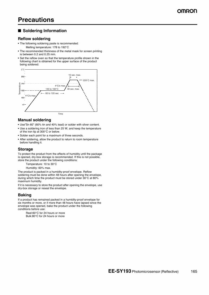
Precautions
■ Soldering Information
Reflow soldering• The following soldering paste is recommended:
Melting temperature: 178 to 192°C• The recommended thickness of the metal mask for screen printing
is between 0.2 and 0.25 mm.• Set the reflow oven so that the temperature profile shown in the
following chart is obtained for the upper surface of the product being soldered.
Manual soldering• Use”Sn 60” (60% tin and 40% lead) or solder with silver content.• Use a soldering iron of less than 25 W, and keep the temperature
of the iron tip at 300°C or below.• Solder each point for a maximum of three seconds.• After soldering, allow the product to return to room temperature
before handling it.
StorageTo protect the product from the effects of humidity until the package is opened, dry-box storage is recommended. If this is not possible, store the product under the following conditions:
Temperature: 10 to 30°CHumidity: 60% max.
The product is packed in a humidity-proof envelope. Reflow soldering must be done within 48 hours after opening the envelope, during which time the product must be stored under 30°C at 80% maximum humidity.If it is necessary to store the product after opening the envelope, use dry-box storage or reseal the envelope.
BakingIf a product has remained packed in a humidity-proof envelope for six months or more, or if more than 48 hours have lapsed since the envelope was opened, bake the product under the following conditions before use:
Reel:60°C for 24 hours or moreBulk:80°C for 24 hours or more
10 sec. max.
220°C max.
Time
60 to 120 secTem
pera
ture
4°C/s max.
40 sec. max.
4°C/s max.
140 to 160°C
EE-SY193 Photomicrosensor (Reflective) 165

Photomicrosensor (Reflective)
EE-SB5(-B)Be sure to read Precautions on page 25.
■ DimensionsNote: All units are in millimeters unless otherwise indicated.
■ Features• Dust-tight construction.• With a visible-light intercepting filter which allows objects to be
sensed without being greatly influenced by the light radiated fromfluorescent lamps.
• Mounted with M3 screws.• Model with soldering terminals (EE-SB5).• Model with PCB terminals (EE-SB5-B).
■ Absolute Maximum Ratings (Ta = 25°C)
Note: 1. Refer to the temperature rating chart if the ambient temper-ature exceeds 25°C.
2. The pulse width is 10 μs maximum with a frequency of100 Hz.
3. Complete soldering within 10 seconds.
■ Electrical and Optical Characteristics (Ta = 25°C)
Note: The letter “d” indicates the distance between the top surface of the sensor and the sensing object.
Internal Circuit
Terminal No. Name
A AnodeK Cathode
C Collector
E Emitter
Dimensions Tolerance
3 mm max. ±0.3
3 < mm ≤ 6 ±0.375
6 < mm ≤ 10 ±0.45
10 < mm ≤ 18 ±0.55
18 < mm ≤ 30 ±0.65
A
K
C
E
Optical axis Optical axisTwo, 3.2±0.2 dia. holes
Four, 0.5
Four, 0.25
EE-SB5 EE-SB5-B
11.5±0.29±0.2
7.62±0.3 2.54±0.22.54±0.2
Unless otherwise specified, the tolerances are as shown below.
Item Symbol Rated value
Emitter Forward current IF 50 mA (see note 1)
Pulse forward cur-rent
IFP 1 A (see note 2)
Reverse voltage VR 4 V
Detector Collector–Emitter voltage
VCEO 30 V
Emitter–Collector voltage
VECO ---
Collector current IC 20 mA
Collector dissipa-tion
PC 100 mW (see note 1)
Ambient tem-perature
Operating Topr –25°C to 80°CStorage Tstg –30°C to 80°C
Soldering temperature Tsol 260°C(see note 3)
Item Symbol Value Condition
Emitter Forward voltage VF 1.2 V typ., 1.5 V max. IF = 30 mA
Reverse current IR 0.01 μA typ., 10 μA max. VR = 4 V
Peak emission wavelength λP 940 nm typ. IF = 20 mA
Detector Light current IL 200 μA min., 2,000 μA max. IF = 20 mA, VCE = 10 VWhite paper with a reflection ratio of 90%, d = 5 mm (see note)
Dark current ID 2 nA typ., 200 nA max. VCE = 10 V, 0 lx
Leakage current ILEAK 2 μA max. IF = 20 mA, VCE = 10 V with no reflec-tion
Collector–Emitter saturated volt-age
VCE (sat) --- ---
Peak spectral sensitivity wave-length
λP 850 nm typ. VCE = 10 V
Rising time tr 30 μs typ. VCC = 5 V, RL = 1 kΩ, IL = 1 mA
Falling time tf 30 μs typ. VCC = 5 V, RL = 1 kΩ, IL = 1 mA
166 EE-SB5(-B) Photomicrosensor (Reflective)

■ Engineering Data
Forward Current vs. Collector Dissipation Temperature Rating
Light Current vs. Forward Current Characteristics (Typical)
Light Current vs. Collector−Emitter Voltage Characteristics (Typical)
Relative Light Current vs. Ambient Temperature Characteristics (Typical)
Dark Current vs. Ambient Temperature Characteristics (Typical)
Response Time vs. Load Resistance Characteristics (Typical)
Sensing Distance Characteristics (Typical)
Response Time Measurement Circuit
Distance d2 (mm)
Sensing Angle Characteristics (Typical)
Angle deviation θ (°)
Input
Output
Input
Output
90 %10 %
VCE = 10 V0lx
IF = 20 mA VCE = 5 V
VCC = 5 V Ta = 25°C
Distance d (mm)
Sensing Position Characteristics (Typical)
Sensing object: White paper with a reflection factor of 90%
Sensing object: White paper with a reflection factor of 90%
IF = 20 mA
IF = 10 mA
IF = 30 mA
IF = 40 mA
Ta = 25°CIF = 20 mAVCE = 10 VSensing object: White paper with a reflection factor of 90%
Sensing object: White paper with a reflection factor of 90%
Ta = 25°C IF = 20 mAVCE = 10 Vd = 5 mm
Sensing object: White paper with a reflection factor of 90%
IF = 20 mAVCE = 10 VTa = 25°C d1 = 5 mm
Sensing Position Characteristics (Typical)
Load resistance RL (kΩ)
Dar
k C
urre
nt I D
(nA
)Ambient temperature Ta (°C)
For
war
d cu
rren
t I F
(m
A)
Forward current IF (mA) Collector−Emitter voltage VCE (V)Li
ght c
urre
nt I
L (m
A)
Ambient temperature Ta (°C) Ambient temperature Ta (°C)R
espo
nse
time
tr, tf
(μs
)
Rel
ativ
e lig
ht c
urre
nt I
L (%
)
Rel
ativ
e lig
ht c
urre
nt I
L (%
)Li
ght c
urre
nt I
L (m
A)
Rel
ativ
e lig
ht c
urre
nt I
L (%
)
IF = 20 mAVCE = 10 VTa = 25°C d1 = 5 mm
Distance d2 (mm)
d = 5 mm Ta = 25°C
Ta = 25°CVCE = 10 Vd = 5 mm
Rel
ativ
e lig
ht c
urre
nt I L
(%
)Li
ght c
urre
nt I L
(μA
)
Sensing object: White paper with a reflection factor of 90%
Col
lect
or d
issi
patio
n P
C (
mW
)
EE-SB5(-B) Photomicrosensor (Reflective) 167

Photomicrosensor (Reflective)
EE-SF5(-B)Be sure to read Precautions on page 25.
■ DimensionsNote: All units are in millimeters unless otherwise indicated.
■ Features• Dust-tight construction.• With a visible-light intercepting filter which allows objects to be
sensed without being greatly influenced by the light radiated fromfluorescent lamps.
• Mounted with M2 screws.• Model with soldering terminals (EE-SF5).• Model with PCB terminals (EE-SF5-B).
■ Absolute Maximum Ratings (Ta = 25°C)
Note: 1. Refer to the temperature rating chart if the ambient temper-ature exceeds 25°C.
2. The pulse width is 10 μs maximum with a frequency of100 Hz.
3. Complete soldering within 10 seconds.
■ Electrical and Optical Characteristics (Ta = 25°C)
Note: The letter “d” indicates the distance between the top surface of the sensor and the sensing object.
Internal Circuit
Terminal No. Name
A AnodeK Cathode
C Collector
E Emitter
Dimensions Tolerance
3 mm max. ±0.3
3 < mm ≤ 6 ±0.375
6 < mm ≤ 10 ±0.45
10 < mm ≤ 18 ±0.55
18 < mm ≤ 30 ±0.65
A
K
C
E
Matted
1.9 dia. 2.2±0.2 dia. hole
Four, 0.25
Four, 0.5
Four, 1.5
EE-SF5 EE-SF5-B
2.54±0.2
2.547.62±0.3
7.6±1
Unless otherwise specified, the tolerances are as shown below.
Item Symbol Rated value
Emitter Forward current IF 50 mA (see note 1)
Pulse forward cur-rent
IFP 1 A (see note 2)
Reverse voltage VR 4 V
Detector Collector–Emitter voltage
VCEO 30 V
Emitter–Collector voltage
VECO ---
Collector current IC 20 mA
Collector dissipa-tion
PC 100 mW (see note 1)
Ambient tem-perature
Operating Topr –25°C to 80°CStorage Tstg –30°C to 80°C
Soldering temperature Tsol 260°C(see note 3)
Item Symbol Value Condition
Emitter Forward voltage VF 1.2 V typ., 1.5 V max. IF = 30 mA
Reverse current IR 0.01 μA typ., 10 μA max. VR = 4 V
Peak emission wavelength λP 940 nm typ. IF = 20 mA
Detector Light current IL 200 μA min., 2,000 μA max. IF = 20 mA, VCE = 10 VWhite paper with a reflection ratio of 90%, d = 5 mm (see note)
Dark current ID 2 nA typ., 200 nA max. VCE = 10 V, 0 lx
Leakage current ILEAK 2 μA max. IF = 20 mA, VCE = 10 V with no reflec-tion
Collector–Emitter saturated volt-age
VCE (sat) --- ---
Peak spectral sensitivity wave-length
λP 850 nm typ. VCE = 10 V
Rising time tr 30 μs typ. VCC = 5 V, RL = 1 kΩ, IL = 1 mA
Falling time tf 30 μs typ. VCC = 5 V, RL = 1 kΩ, IL = 1 mA
168 EE-SF5(-B) Photomicrosensor (Reflective)

■ Engineering Data
Sensing object
Forward Current vs. Collector Dissipation Temperature Rating
Light Current vs. Forward Current Characteristics (Typical)
Light Current vs. Collector−Emitter Voltage Characteristics (Typical)
Relative Light Current vs. Ambient Temperature Characteristics (Typical)
Dark Current vs. Ambient Temperature Characteristics (Typical)
Response Time vs. Load Resistance Characteristics (Typical)
Sensing Distance Characteristics (Typical)
Response Time Measurement Circuit
Sensing Angle Characteristics (Typical)
Input
Output
Input
Output
90 %10 %
Distance d (mm)
Sensing Position Characteristics (Typical)
Sensing Position Characteristics (Typical)
Sensing Angle Characteristics (Typical)
Sensing object: White paper with a reflection factor of 90%
Ta = 25°CVCE = 10 Vd = 5 mm
Sensing object: White paper with a reflection factor of 90%
d1 = 5 mm
Phototransistor sideLED side
(a) : d1 = 3 mm (b) : d1 = 5 mm
d1
d = 5 mm
Distance d2 (mm)
Angle deviation θ (°)
VCE = 10 V0lx
IF = 20 mA VCE = 5 V
VCC = 5 V Ta = 25°C
Rel
ativ
e lig
ht c
urre
nt I L
(%
)
Sensing object: White paper with a reflection factor of 90%
IF = 20 mA
IF = 10 mA
IF = 30 mA
IF = 40 mA
Ta = 25°CVCE = 10 V
Sensing object: White paper with a reflection factor of 90%
Ta = 25°C IF = 20 mAVCE = 10 V
IF = 20 mAVCE = 5 VTa = 25°C
Ligh
t cur
rent
I L (
μA)
Load resistance RL (kΩ)
Dar
k C
urre
nt I D
(nA
)Ambient temperature Ta (°C)
For
war
d cu
rren
t I F
(m
A)
Forward current IF (mA) Collector−Emitter voltage VCE (V)Li
ght c
urre
nt I
L (m
A)
Ambient temperature Ta (°C) Ambient temperature Ta (°C)R
espo
nse
time
tr, tf
(μs
)
Rel
ativ
e lig
ht c
urre
nt I
L (%
)
Rel
ativ
e lig
ht c
urre
nt I
L (%
)Li
ght c
urre
nt I
L (m
A)
Rel
ativ
e lig
ht c
urre
nt I
L (%
)
Distance d2 (mm)
d = 5 mm Ta = 25°C
Sensing object: White paper with a reflection factor of 90%
IF = 20 mAVCE = 5 VTa = 25°C d1 = 5 mmSensing object: White paper with a reflection factor of 90%
Angle deviation θ (°)
Rel
ativ
e lig
ht c
urre
nt I
L (%
)
d = 5 mmSensing object: White paper with a reflection factor of 90%
Ta = 25°C IF = 20 mAVCE = 10 V
Col
lect
or d
issi
patio
n P
C (
mW
)
EE-SF5(-B) Photomicrosensor (Reflective) 169

Photomicrosensor (Reflective)
EE-SY310/-SY410Be sure to read Precautions on page 25.
■ DimensionsNote: All units are in millimeters unless otherwise indicated.
■ Features• Incorporates an IC chip with a built-in detector element and ampli-
fier.• Incorporates a detector element with a built-in temperature com-
pensation circuit.• Compact reflective model with a molded housing.• A wide supply voltage range: 4.5 to 16 VDC• Directly connects with C-MOS and TTL.• Dark ON model (EE-SY310)• Light ON model (EE-SY410)
■ Absolute Maximum Ratings (Ta = 25°C)
Note: 1. Refer to the temperature rating chart if the ambient temper-ature exceeds 25°C.
2. The pulse width is 10 μs maximum with a frequency of100 Hz.
3. Complete soldering within 10 seconds.
■ Electrical and Optical Characteristics (Ta = 25°C)
Internal Circuit
Dimensions Tolerance
3 mm max. ±0.2
3 < mm ≤ 6 ±0.24
6 < mm ≤ 10 ±0.29
10 < mm ≤ 18 ±0.35
18 < mm ≤ 30 ±0.42
Terminal No. Name
A Anode
K Cathode
V Power supply (Vcc)
O Output (OUT)
G Ground (GND)
A
K
V
G
O
Five, 0.3
Two. R2Two. R1.5
15 to 1817 to 24
Five, 0.5
Unless otherwise specified, the tolerances are as shown below.
4.6 +0.2−0.3
Item Symbol Rated value
Emitter Forward current IF 50 mA (see note 1)
Reverse voltage VR 4 V
Pulse forward current
IFP 1 A (see note 2)
Detector Power supply voltage
VCC 16 V
Output voltage VOUT 28 V
Output current IOUT 16 mA
Permissible out-put dissipation
POUT 250 mW (see note 1)
Ambient tempera-ture
Operating Topr –40°C to 75°CStorage Tstg –40°C to 85°C
Soldering temperature Tsol 260°C(see note 3)
Item Symbol Value Condition
Emitter Forward voltage VF 1.2 V typ., 1.5 V max. IF = 20 mA
Reverse current IR 0.01 μA typ., 10 μA max. VR = 4 V
Peak emission wavelength λP 920 nm typ. IF = 20 mA
Detector Low-level output voltage VOL 0.12 V typ., 0.4 V max. Vcc = 4.5 to 16 V, IOL = 16 mA,without incident light (EE-SY310), with incident light (EE-SY410) (see notes 1 and 2)
High-level output voltage VOH 15 V min. Vcc = 16 V, RL = 1 kΩ,with incident light (EE-SY310), without incident light (EE-SY410) (see notes 1 and 2)
Current consumption ICC 3.2 mA typ., 10 mA max. Vcc = 16 V
Peak spectral sensitivity wavelength
λP 870 nm typ. VCC = 4.5 to 16 V
LED current when output is OFF IFT 6 mA typ., 15 mA max. VCC = 4.5 to 16 V
LED current when output is ON
Hysteresis ΔH 17% typ. VCC = 4.5 to 16 V
Response frequency f 50 Hz min. VCC = 4.5 to 16 V, IF = 15 mA, IOL = 16 mA
Response delay time tPLH (tPHL) 3 μs typ. VCC = 4.5 to 16 V, IF = 15 mA, IOL = 16 mA
Response delay time tPHL (tPLH) 20 μs typ. VCC = 4.5 to 16 V, IF = 15 mA, IOL = 16 mA
170 EE-SY310/-SY410 Photomicrosensor (Reflective)

■ Engineering DataNote: The values in the parentheses apply to the EE-SY410.
Input
Output
Input
Output
EE-SY310 EE-SY410
200 mm dia.
15 mm
5 mm
15 mm15 mm
(tPLH) (tPHL) (tPLH)(tPHL)
Note: 1. With incident light" denotes the condition whereby the light reflected by white paper with a reflection factor of 90% at a sensing distance of 5 mm is received by the photo IC when the forward current (IF) of the LED is 20 mA.
2. Sensing object: White paper with a reflection factor of 90% at a sensing distance of 5 mm.
3. Hysteresis denotes the difference in forward LED current value, expressed in percentage, calculated from the respective forward LED currents when the photo IC is turned from ON to OFF and when the photo IC is turned from OFF to ON.
4. The value of the response frequency is measured by rotating the disk as shown below.
5. The following illustrations show the definition of response delay time. The value in the parentheses applies to the EE-SY410.
Forward Current vs. Collector Dissipation Temperature Rating
Forward Current vs. Forward Voltage Characteristics (Typical)
LED Current vs. Supply Voltage (Typical)
LED Current vs. Ambient Temperature Characteristics (Typical)
Low-level Output Voltage vs. Output Current (Typical)
Current Consumption vs. Supply Voltage (Typical)
Response Delay Time vs. Forward Current (Typical)
Sensing Position Characteristics (Typical)
Low-level Output Voltage vs. Ambient Temperature Characteristics (Typical)
Dis
tanc
e d 2
(m
m)
Distance d1 (mm)
IFT OFF (IFT ON)
IFT ON (IFT OFF)
IFT OFF (IFT ON)
IFT ON (IFT OFF)
IOL = 16 mA
IOL = 5 mA
VOUT
(EE-SY3@@)VOUT
(EE-SY4@@)
tPHL (tPLH)
Sensing object: White paper with a reflection factor of 90%
IF = 20 mA VCC = 5 V Ta = 25°C
Operate
Release
Cur
rent
con
sum
ptio
n Ic
c (m
A)
Forward voltage VF (V) Supply voltage VCC (V)
Low
leve
l out
put v
olta
ge V
OL
(V)
Supply voltage VCC (V) Forward current IF (mA)
VCC = 5 V IF = 0 mA (15 mA)
Ta = 25°C IF = 0 mA (15 mA)
VCC = 5 V RL = 330 Ω Ta = 25°C
Ambient temperature Ta (°C)
Out
put a
llow
able
dis
sipa
tion
PC (
mW
)
For
war
d cu
rren
t I F
(m
A)
For
war
d cu
rren
t I F
(m
A)
LED
cur
rent
IF
T (
mA
)
Ta = 25°CRL = 1 kΩ
Res
pons
e de
lay
time
t PH
L, t P
LH (
μs)
VCC = 5 V Ta = 25°C
LED
cur
rent
IF
T (
mA
)
Ambient temperature Ta (°C)
VCC = 5 VRL = 330 Ω
Ta = −30°C
Ta = 25°C
Ta = 70°C
Low
leve
l out
put v
olta
ge V
OL
(V)
Output current IOUT (mA) Ambient temperature Ta (°C)
IF = 0 mA (15 mA)
EE-SY310/-SY410 Photomicrosensor (Reflective) 171

Photomicrosensor (Reflective)
EE-SY313/-SY413Be sure to read Precautions on page 25.
■ DimensionsNote: All units are in millimeters unless otherwise indicated.
■ Features• Incorporates an IC chip with a built-in detector element and ampli-
fier.• Incorporates a detector element with a built-in temperature com-
pensation circuit.• Compact reflective Photomicrosensor (EE-SY310/-SY410) with a
molded housing and a dust-tight cover.• A wide supply voltage range: 4.5 to 16 VDC• Directly connects with C-MOS and TTL.• Dark ON model (EE-SY313)• Light ON model (EE-SY413)
■ Absolute Maximum Ratings (Ta = 25°C)
Note: 1. Refer to the temperature rating chart if the ambient temper-ature exceeds 25°C.
2. The pulse width is 10 μs maximum with a frequency of100 Hz.
3. Complete soldering within 10 seconds.
■ Electrical and Optical Characteristics (Ta = 25°C)
Internal Circuit
Dimensions Tolerance
3 mm max. ±0.3
3 < mm ≤ 6 ±0.375
6 < mm ≤ 10 ±0.45
10 < mm ≤ 18 ±0.55
18 < mm ≤ 30 ±0.65
Terminal No. Name
A Anode
K Cathode
V Power supply (Vcc)
O Output (OUT)
G Ground (GND)
A
K
V
G
O
Five, 0.5
15 to 1817 to 24
Unless otherwise specified, the tolerances are as shown below.
Item Symbol Rated value
Emitter Forward current IF 50 mA (see note 1)
Reverse voltage VR 4 V
Pulse forward current
IFP 1 A (see note 2)
Detector Power supply voltage
VCC 16 V
Output voltage VOUT 28 V
Output current IOUT 16 mA
Permissible output dissipa-tion
POUT 250 mW (see note 1)
Ambient tem-perature
Operating Topr –40°C to 65°CStorage Tstg –40°C to 85°C
Soldering temperature Tsol 260°C(see note 3)
Item Symbol Value Condition
Emitter Forward voltage VF 1.2 V typ., 1.5 V max. IF = 20 mA
Reverse current IR 0.01 μA typ., 10 μA max. VR = 4 V
Peak emission wave-length
λP 920 nm typ. IF = 20 mA
Detector Low-level output voltage VOL 0.12 V typ., 0.4 V max. Vcc = 4.5 to 16 V, IOL = 16 mA, without incident light (EE-SY313), with incident light (EE-SY413) (see notes 1 and 2)
High-level output volt-age
VOH 15 V min. Vcc = 16 V, RL = 1 kΩ, with incident light (EE-SY313), with-out incident light (EE-SY413) (see notes 1 and 2)
Current consumption ICC 3.2 mA typ., 10 mA max. Vcc = 16 V
Peak spectral sensitivity wavelength
λP 870 nm typ. VCC = 4.5 to 16 V
LED current when output is OFF IFT 10 mA typ., 20 mA max. VCC = 4.5 to 16 V
LED current when output is ON
Hysteresis ΔH 17% typ. VCC = 4.5 to 16 V
Response frequency f 50 pps min. VCC = 4.5 to 16 V, IF = 20 mA, IOL = 16 mA
Response delay time tPLH (tPHL) 3 μs typ. VCC = 4.5 to 16 V, IF = 20 mA, IOL = 16 mA
Response delay time tPHL (tPLH) 20 μs typ. VCC = 4.5 to 16 V, IF = 20 mA, IOL = 16 mA
172 EE-SY313/-SY413 Photomicrosensor (Reflective)

■ Engineering DataNote: The values in the parentheses apply to the EE-SY413.
Input
Output
Input
Output
EE-SY313 EE-SY413
200 mm dia.
15 mm
4.4 mm
15 mm15 mm
(tPLH) (tPHL) (tPLH)(tPHL)
Note: 1. With incident light" denotes the condition whereby the light reflected by white paper with a reflection factor of 90% at a sensing distance of 4.4 mm is received by the photo IC when the forward current (IF) of the LED is 20 mA.
2. Sensing object: White paper with a reflection factor of 90% at a sensing distance of 4.4 mm.
3. Hysteresis denotes the difference in forward LED current value, expressed in percentage, calculated from the respective forward LED currents when the photo IC is turned from ON to OFF and when the photo IC is turned from OFF to ON.
4. The value of the response frequency is measured by rotating the disk as shown below.
5. The following illustrations show the definition of response delay time. The value in the parentheses applies to the EE-SY413.
Forward Current vs. Collector Dissipation Temperature Rating
Forward Current vs. Forward Voltage Characteristics (Typical)
LED Current vs. Supply Voltage (Typical)
LED Current vs. Ambient Temperature Characteristics (Typical)
Low-level Output Voltage vs. Output Current (Typical)
Current Consumption vs. Supply Voltage (Typical)
Response Delay Time vs. Forward Current (Typical)
Sensing Position Characteristics (Typical)
Low-level Output Voltage vs. Ambient Temperature Characteristics (Typical)
tPLH (tPHL)
Sensing object: White paper with a reflection factor of 90%
Operate
Release
Dis
tanc
e d 2
(m
m)
Distance d1 (mm)
IFT OFF (IFT ON)
IFT ON (IFT OFF)
IFT OFF (IFT ON)
IFT ON (IFT OFF)
IOL = 16 mA
IOL = 5 mA
VOUT
(EE-SY3@@)VOUT
(EE-SY4@@)
tPHL (tPLH)
IF = 20 mA VCC = 5 V Ta = 25°C
Cur
rent
con
sum
ptio
n Ic
c (m
A)
Forward voltage VF (V) Supply voltage VCC (V)
Low
leve
l out
put v
olta
ge V
OL
(V)
Supply voltage VCC (V) Forward current IF (mA)
VCC = 5 V IF = 0 mA (20 mA)
Ta = 25°C IF = 0 mA (15 mA)
VCC = 5 V RL = 330 Ω Ta = 25°C
Ambient temperature Ta (°C)
Out
put a
llow
able
dis
sipa
tion
PC (
mW
)
For
war
d cu
rren
t I F
(m
A)
For
war
d cu
rren
t I F
(m
A)
LED
cur
rent
IF
T (
mA
)
Ta = 25°CRL = 1 kΩ
Res
pons
e de
lay
time
t PH
L, t P
LH (
μs)
VCC = 5 V Ta = 25°C
LED
cur
rent
IF
T (
mA
)
Ambient temperature Ta (°C)
VCC = 5 VRL = 330 Ω
Ta = −30°C
Ta = 25°C
Ta = 70°C
Low
leve
l out
put v
olta
ge V
OL
(V)
Output current IC (mA) Ambient temperature Ta (°C)
IF = 0 mA (20 mA)
EE-SY313/-SY413 Photomicrosensor (Reflective) 173

174 EE-SY313/-SY413 Photomicrosensor (Reflective)

175
InformationReliability . . . . . . . . . . . . . . . . . . . . . . . . . . . . . . . . . . . . . . . . . . . . . . . . . . . 176Security Trade Control . . . . . . . . . . . . . . . . . . . . . . . . . . . . . . . . . . . . . . . . . 185

Reliability
■ Market Product QualityOMRON is making efforts so that OMRON’s Photomicrosensors can achieve a failure rate of only 10–7/h.OMRON will continue improving the quality of its products to comply with OMRON Photomicrosensors users’ demand for product quality whileactively providing good after-sales service.OMRON’s Photomicrosensors achieved a failure rate of 10 ppm. Figure 5 shows the reasons for the return of OMRON Photomicrosensors.The reasons for approximately two-thirds of the products sent back were that they were not working or they were destroyed. It is possible that theywere not working or they were destructed because excessive voltages were imposed on them or they were not operated properly according to theirspecifications. To solve such problems, OMRON is actively holding preliminary meetings with customers who will use OMRON products and advisethem of the operating conditions required by the products while actively providing them with after-sales service.
■ ReliabilityThe life of any Photomicrosensor depends on the secular changes of the optical output of the LED built into the Photomicrosensor. The followingare the output characteristics of the Photomicrosensor, all of which depend on the optical output of the LED.
OMRON has been conducting reliability tests of each type of Photomicrosensor to check the secular changes of the optical output of the LED builtinto the Photomicrosensor.
Phototransistor output Light current (IL)
Photo IC output LED current IFT with the photo IC output ON and OFF
Amplifier output (reflective sensor) Sensing distance d
Element problems
Design problems Other
Destruction
Not working
Component problems
Figure 5. Reasons for Products Sent Back
(35.3%)
(28.4%)
(27.0%)
(7.2%)
(0.4%)(1.8%)
176 Product Quality Control and Reliability

■ Reliability TestsIn principle, Photomicrosensors conform to JEITA standards. The following table shows the details of the reliability tests of Photomicrosensors con-ducted by OMRON.
Figure 6. Details of Reliability Tests
Classification Test Detail Conforming standard
Thermal con-dition test
Soldering heat resistivity
Evaluates the soldering heat resistivity of products. Usually, this test is conducted under the following conditions.Soldering temperature: 260±5°CSoldering time:10±1 s
JEITA ED-4701/300ED-8121
JIS C7021: A1IEC Pub68-2-20
Thermal shock Evaluates the resistivity of products to radical temperature changes. Usually, this test is conducted under the following conditions.Ta: 0°C to 100°C (liquid bath) or TstgMIN to TstgMAX (liquid bath)
JEITA ED-4701/300JIS C7021: A3IEC Pub68-2-14
Temperature cy-cle
JEITA ED-4701/100JIS C7021: A4IEC Pub68-2-14
The five-minute storage periods at a temperature of 25°C in the test may be omitted.
Temperature and humidity cy-cle
JEITA ED-4701/200JIS C7021: A5IEC Pub68-2-4
Mechanical test
Soldering ease Evaluates the terminal soldering ease of the products. Usu-ally, this test is conducted under the following conditions.Soldering temperature: 230±5°CSoldering time: 5±0.5 s
JEITA ED-4701/300ED-8121
JIS C7021: A2IEC Pub68-2-20
Terminal strength
Evaluates the resistivity of the terminals of products to the force imposed on the terminals while the products are mounted, wired, or operated.
1. Tension testOn each terminal of products, a specified load isimposed for 10±1 s in the direction of the terminal.
2. Bending testOn the tip of each terminal of products, a specified loadis imposed to bend the terminal by 90° and to change itback.
JEITA ED-4701/400ED-8121
JIS C7021: A11IEC Pub68-2-21
Shock resis-tance
Judges the structural resistivity and mechanical resistivity of products. The conditions of this test vary with the product structure. Usually, this test is conducted under the following conditions.Impact acceleration:14,700 m/s2
Pulse width: 0.5 ms
JEITA ED-4701/400ED-8121
JIS C7021: A7IEC Pub68-2-27
A product may be sub-jected to this test after it is packed up.
Vibration resis-tance
Evaluates the vibration resistivity of products while they are transported or operated. Usually, this test is conducted under the following conditions.Frequency: 100 to 2000 Hz/4 min200 m/s2
JEITA ED-4701/400ED-8121
JIS C7021: A10IEC Pub68-2-21
A product may be sub-jected to this test after it is packed up.
Natural drop Evaluates the irregular shock resistivity of products while they are handled, transported, or operated. Usually, this test is conducted under the following conditions.Height: 75 cmNo. of times: 3
JEITA EIAJ-8121JIS C7021: A8IEC Pub68-2-32
A product may be sub-jected to this test after it is packed up.
Evaluates the low- and high-temperature resistivity of products.
Tstg min.(30 min)
25°C(5 min)
Tstg max.(30 min)
25°C(5 min)
1 cycle
Evaluates the high-temperature and high-humidity resistivity of products.
1 cycle
25°C
65°C 90% to 95%
−10°C24 h
10 cycles
Product Quality Control and Reliability 177

Note: The above testing conditions and testing times depend on the features of each product.
Life expectan-cy test
Continuous op-eration
Evaluates the resistivity of products to a continuous, long-time electrical stress and temperature stress. Usually, this test is conducted under the following conditions.Ta: 25±5°CBias: IFMAX or PCMAX
EIAJ-EDX-8121EIAJ-SD-121: 201JIS C7021: B4
A product may be sub-jected to this test at a high temperature, low temperature, or high temperature and humid-ity.
High-tempera-ture storage
Evaluates the resistivity of products to a high-storage tem-perature for a long time. Usually, this test is conducted under the following conditions.Ta: TstgMAXTime: 1,000 hrs
EIAJ-EDX-8121EIAJ-SD-121: 115JIS C7021: B10IEC Pub68-2-2
Low-tempera-ture storage
Evaluates the resistivity of products to a low-storage temper-ature for a long time. Usually, this test is conducted under the following conditions.Ta: TstgMINTime: 1,000 hrs
EIAJ-EDX-8121EIAJ-SD-121: 116JIS C7021: B12IEC Pub68-2-1
High-tempera-ture and high-humidity stor-age
Evaluates the resistivity of products to a high-storage tem-perature and high storage humidity for a long time. Usually, this test is conducted under the following conditions.Ta: 60°CHumidity: 90%Time: 1,000 hrs
EIAJ-EDX-8121EIAJ-SD-121: 117JIS C7021: B11IEC Pub68-2-3
High-tempera-ture reverse bias
Evaluates the resistivity of products to a continuous electrical stress and temperature stress.
EIAJ-SD-121: 203JIS C7021: B8
A product may be sub-jected to this test at a low temperature, high temperature, or high hu-midity.
Classification Test Detail Conforming standard
178 Product Quality Control and Reliability

■ Data from Reliability TestsThe following tables show the results of the reliability tests of typical Transmissive Photomicrosensors with an Infrared LED conducted by OMRON.
Providing this data does not imply that OMRON guarantees the specified reliability level.
Typical Failure Rates (MTTF Data)
EE-SX1041 (Transmissive Phototransistor Output)
Failure Criteria
Note: Except life test.
Test Results
Note: 1. The tests after 1001 hours are for reference only.2. Confidence level of 90%.
Item Symbol Measuring conditions
Failure criteria
General test (see note) Life test
Forward voltage VF IF = 30 mA 1.5 V max. 1.8 V max.
Reverse current IR VR = 4 V 10 μA max. 20 μA max.
Dark current ID VCE = 10 V 0lx 200 nA max. 400 nA max.
Light current IL IF = 20 mAVCE = 10 V
0.5 mA min.14 mA max.
Initial value × 0.7 min.
Test item Test conditions (see note 1) Number of samples
Component hours (h)
Number of failures Failure rate (1/h) (see note 2)
Continuous operation Ta = 25°C, IF = 50 mA2000 h
22 pcs 4.4 x 10⁴ 0 5.22 x 10⁻⁵
High-temperature stor-age
Ta = 100°C2000 h
22 pcs 4.4 x 10⁴ 0 5.22 x 10⁻⁵
Low-temperature stor-age
Ta = –30°C2000 h
22 pcs 4.4 x 10⁴ 0 5.22 x 10⁻⁵
High-temperature and high-humidity storage
Ta = 60°C, 90%2000 h
22 pcs 4.4 x 10⁴ 0 5.22 x 10⁻⁵
High-temperature re-verse bias
Ta = 85°C, VCE = 30 V2000 h
22 pcs 4.4 x 10⁴ 0 5.22 x 10⁻⁵
Temperature cycle –30°C (30 min) to 100°C (30 min) 10 times
22 pcs --- 0 ---
Shock resistance 14,700 m/s2, 0.5 ms, 3 times each in ±X, ±Y, and ±Z directions
11 pcs --- 0 ---
Vibration resistance 20 to 2,000 Hz, 1.5 mm or 98 m/s2 each in X, Y, and Z direc-tions
11 pcs --- 0 ---
Product Quality Control and Reliability 179

EE-SX1235A-P2 (Transmissive Phototransistor Output)
Failure Criteria
Note: Except life test.
Test Results
Note: 1. The tests after 1001 hours are for reference only.2. Confidence level of 90%.
Item Symbol Measuring conditions
Failure criteria
General test (see note) Life test
Forward voltage VF IF = 30 mA 1.5 V max. 1.8 V max.
Reverse current IR VR = 4 V 10 μA max. 20 μA max.
Dark current ID VCE = 10 V 0lx 200 nA max. 400 nA max.
Light current IL IF = 20 mAVCE = 5 V
0.5 mA min.14 mA max.
Initial value × 0.7 min.
Test item Test conditions (see note 1) Number of samples
Component hours (h)
Number of failures Failure rate (1/h) (see note 2)
Continuous operation Ta = 25°C, IF = 50 mA2000 h
22 pcs 4.4 x 10⁴ 0 5.22 x 10⁻⁵
High-temperature stor-age
Ta = 100°C2000 h
22 pcs 4.4 x 10⁴ 0 5.22 x 10⁻⁵
Low-temperature stor-age
Ta = –40°C2000 h
22 pcs 4.4 x 10⁴ 0 5.22 x 10⁻⁵
High-temperature and high-humidity storage
Ta = 60°C, 90%2000 h
22 pcs 4.4 x 10⁴ 0 5.22 x 10⁻⁵
High-temperature re-verse bias
Ta = 85°C, VCE = 30 V2000 h
22 pcs 4.4 x 10⁴ 0 5.22 x 10⁻⁵
Temperature cycle –40°C (30 min) to 100°C (30 min) 10 times
22 pcs --- 0 ---
Shock resistance 294 m/s2, 0.5 ms, 3 times each in ±X, ±Y, and ±Z directions
11 pcs --- 0 ---
Vibration resistance 5 to 50 Hz, 1.5 mm or 9.8 m/s2 each in X, Y, and Z directions
11 pcs --- 0 ---
180 Product Quality Control and Reliability

EE-SX398 (Transmissive Photo-IC Output)
Failure Criteria
Note: Except life test.
Test Results
Note: 1. The tests after 1001 hours are for reference only.2. Confidence level of 90%.
Item Symbol Measuring conditions
Failure criteria
General test (see note) Life test
Forward voltage VF IF = 20 mA 1.5 V max. 1.8 V max.
Reverse current IR VR = 4 V 10 μA max. 20 μA max.
Low-level output voltage
VOL VCC = 16 V
IOL = 16 mA
IF = 0 mA
0.4 V max. 0.48 V max.
High-level output current
IOH VCC = 16 V
VOUT = 28 V
IF = 5 mA
100 μA max. 200 μA max.
Current consump-tion
ICC VCC = 16 V 10 mA max. 12 mA max.
LED current when output is OFF
IFT VCC = 16 V
IOL = 16 mA
5 mA max. Initial value × 1.3 max.
Test item Test conditions (see note 1) Number of samples
Component hours (h)
Number of failures Failure rate (1/h) (see note 2)
Continuous operation Ta = 25°C, IF = 20 mA, VCC = 5 V1500 h
22 pcs 3.3 x 10⁴ 0 6.96 x 10⁻⁵
High-temperature stor-age
Ta = 100°C2000 h
22 pcs 3.3 x 10⁴ 0 6.96 x 10⁻⁵
Low-temperature stor-age
Ta = –40°C2000 h
22 pcs 3.3 x 10⁴ 0 6.96 x 10⁻⁵
High-temperature and high-humidity storage
Ta = 60°C, 90%2000 h
22 pcs 3.3 x 10⁴ 0 6.96 x 10⁻⁵
High-temperature re-verse bias
Ta = 85°C, VCE = 30 V2000 h
22 pcs 3.3 x 10⁴ 0 6.96 x 10⁻⁵
Temperature cycle –40°C (30 min) to 100°C (30 min) 10 times
22 pcs --- 0 ---
Shock resistance 14,700 m/s2, 0.5 ms, 3 times each in ±X, ±Y, and ±Z directions
11 pcs --- 0 ---
Vibration resistance 20 to 2,000 Hz, 1.5 mm or 98 m/s2 each in X, Y, and Z direc-tions
11 pcs --- 0 ---
Product Quality Control and Reliability 181
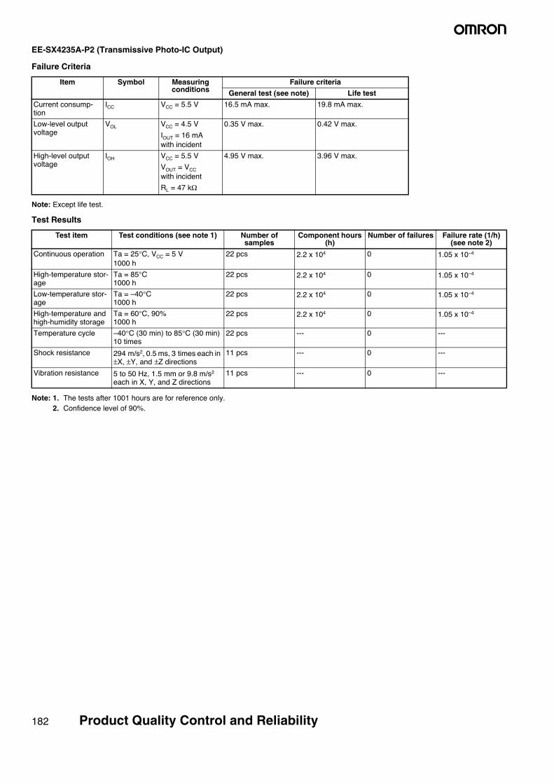
EE-SX4235A-P2 (Transmissive Photo-IC Output)
Failure Criteria
Note: Except life test.
Test Results
Note: 1. The tests after 1001 hours are for reference only.2. Confidence level of 90%.
Item Symbol Measuring conditions
Failure criteria
General test (see note) Life test
Current consump-tion
ICC VCC = 5.5 V 16.5 mA max. 19.8 mA max.
Low-level output voltage
VOL VCC = 4.5 V
IOUT = 16 mA with incident
0.35 V max. 0.42 V max.
High-level output voltage
IOH VCC = 5.5 V
VOUT = VCC
with incident
RL = 47 kΩ
4.95 V max. 3.96 V max.
Test item Test conditions (see note 1) Number of samples
Component hours (h)
Number of failures Failure rate (1/h) (see note 2)
Continuous operation Ta = 25°C, VCC = 5 V1000 h
22 pcs 2.2 x 10⁴ 0 1.05 x 10⁻⁴
High-temperature stor-age
Ta = 85°C1000 h
22 pcs 2.2 x 10⁴ 0 1.05 x 10⁻⁴
Low-temperature stor-age
Ta = –40°C1000 h
22 pcs 2.2 x 10⁴ 0 1.05 x 10⁻⁴
High-temperature and high-humidity storage
Ta = 60°C, 90%1000 h
22 pcs 2.2 x 10⁴ 0 1.05 x 10⁻⁴
Temperature cycle –40°C (30 min) to 85°C (30 min) 10 times
22 pcs --- 0 ---
Shock resistance 294 m/s2, 0.5 ms, 3 times each in ±X, ±Y, and ±Z directions
11 pcs --- 0 ---
Vibration resistance 5 to 50 Hz, 1.5 mm or 9.8 m/s2 each in X, Y, and Z directions
11 pcs --- 0 ---
182 Product Quality Control and Reliability
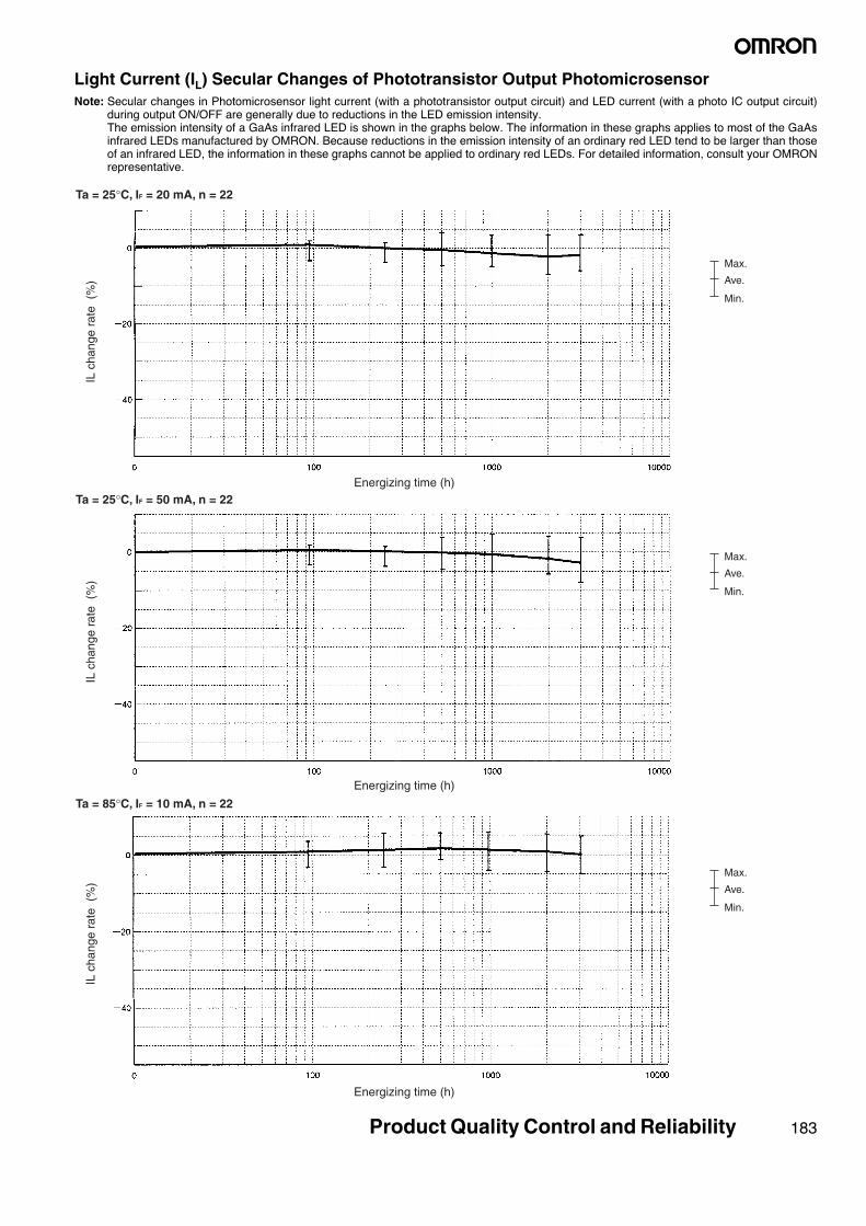
Light Current (IL) Secular Changes of Phototransistor Output PhotomicrosensorNote: Secular changes in Photomicrosensor light current (with a phototransistor output circuit) and LED current (with a photo IC output circuit)
during output ON/OFF are generally due to reductions in the LED emission intensity.The emission intensity of a GaAs infrared LED is shown in the graphs below. The information in these graphs applies to most of the GaAsinfrared LEDs manufactured by OMRON. Because reductions in the emission intensity of an ordinary red LED tend to be larger than thoseof an infrared LED, the information in these graphs cannot be applied to ordinary red LEDs. For detailed information, consult your OMRONrepresentative.
Ta = 25°C, IF = 20 mA, n = 22
Ta = 25°C, IF = 50 mA, n = 22
Ta = 85°C, IF = 10 mA, n = 22
IL c
hang
e ra
te (
%)
Energizing time (h)
Max.
Ave.
Min.
IL c
hang
e ra
te (
%)
Energizing time (h)
IL c
hang
e ra
te (
%)
Energizing time (h)
Max.
Ave.
Min.
Max.
Ave.
Min.
Product Quality Control and Reliability 183

Ta = −25°C, IF = 50 mA, n = 22
IL c
hang
e ra
te (
%)
Energizing time (h)
Max.
Ave.
Min.
184 Product Quality Control and Reliability
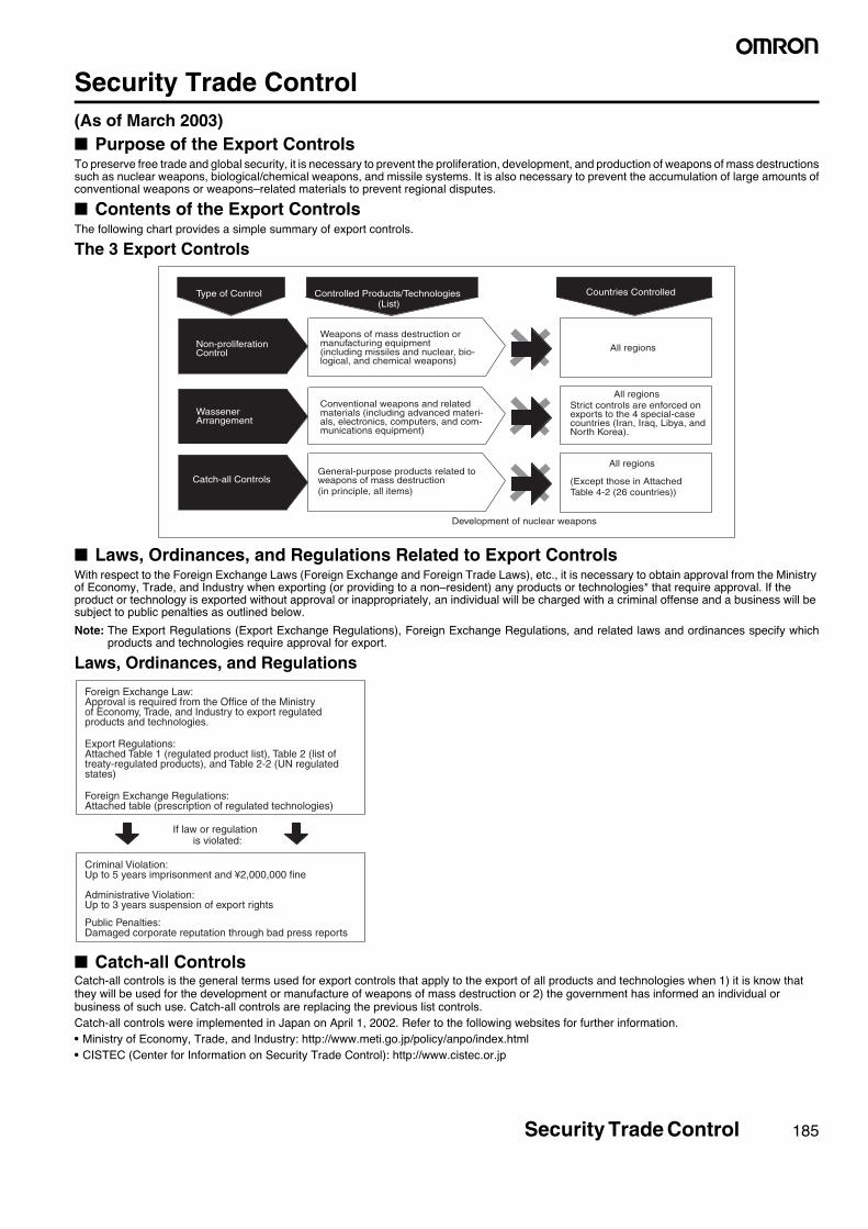
Security Trade Control(As of March 2003)■ Purpose of the Export ControlsTo preserve free trade and global security, it is necessary to prevent the proliferation, development, and production of weapons of mass destructionssuch as nuclear weapons, biological/chemical weapons, and missile systems. It is also necessary to prevent the accumulation of large amounts ofconventional weapons or weapons–related materials to prevent regional disputes.
■ Contents of the Export ControlsThe following chart provides a simple summary of export controls.
The 3 Export Controls
■ Laws, Ordinances, and Regulations Related to Export ControlsWith respect to the Foreign Exchange Laws (Foreign Exchange and Foreign Trade Laws), etc., it is necessary to obtain approval from the Ministry of Economy, Trade, and Industry when exporting (or providing to a non–resident) any products or technologies* that require approval. If the product or technology is exported without approval or inappropriately, an individual will be charged with a criminal offense and a business will be subject to public penalties as outlined below.
Note: The Export Regulations (Export Exchange Regulations), Foreign Exchange Regulations, and related laws and ordinances specify whichproducts and technologies require approval for export.
Laws, Ordinances, and Regulations
■ Catch-all ControlsCatch-all controls is the general terms used for export controls that apply to the export of all products and technologies when 1) it is know that they will be used for the development or manufacture of weapons of mass destruction or 2) the government has informed an individual or business of such use. Catch-all controls are replacing the previous list controls.Catch-all controls were implemented in Japan on April 1, 2002. Refer to the following websites for further information. • Ministry of Economy, Trade, and Industry: http://www.meti.go.jp/policy/anpo/index.html• CISTEC (Center for Information on Security Trade Control): http://www.cistec.or.jp
Conventional weapons and related materials (including advanced materi-als, electronics, computers, and com-munications equipment)
All regions
Type of Control Controlled Products/Technologies(List)
Countries Controlled
Non-proliferationControl
Wassener Arrangement
Catch-all Controls
Weapons of mass destruction or manufacturing equipment(including missiles and nuclear, bio-logical, and chemical weapons)
General-purpose products related to weapons of mass destruction (in principle, all items)
All regionsStrict controls are enforced on exports to the 4 special-case countries (Iran, Iraq, Libya, and North Korea).
All regions
(Except those in Attached Table 4-2 (26 countries))
Development of nuclear weapons
If law or regulation is violated:
Foreign Exchange Law:Approval is required from the Office of the Ministry of Economy, Trade, and Industry to export regulatedproducts and technologies.
Export Regulations:Attached Table 1 (regulated product list), Table 2 (list of treaty-regulated products), and Table 2-2 (UN regulated states)
Foreign Exchange Regulations:Attached table (prescription of regulated technologies)
Criminal Violation:Up to 5 years imprisonment and ¥2,000,000 fine
Administrative Violation:Up to 3 years suspension of export rights
Public Penalties:Damaged corporate reputation through bad press reports
Security Trade Control 185
■ Compliance with the RegulationsAs a corporate citizen of Japan and the global community, OMRON has established a Compliance Program to assure compliance with the regulations outlined above in order to help maintain free trade and global security. We have also planned a training course on export controls.OMRON determines whether each of its products is subject to export controls and carefully controls transactions so that OMRON products are not exported inappropriately.
■ Request to CustomersWhen exporting goods that require export approval, always obtain approval from an Official of the Ministry of Economy, Trade, and Industry. When dealing with products that are subject to export controls, take precautions to prevent incorrect exportation even when the products are resold.When exporting a controlled product, check the final application and end user to verify that the product will not be used in a weapon–related application such as a weapon itself or weapons research.Furthermore, always verify that the OMRON product will not be used in any case in a nuclear weapon, missile, chemical weapon, other weapon, or equipment used to manufacture these weapons.The limitations described above will be submitted to OMRON or an OMRON sales representative as an approval form or contract, so please fully understand and comply with these procedures.If you have any questions, please contact your OMRON representative for further details. These security procedures are based on domestic Japanese laws and apply to exports from Japan.
186 Security Trade Control
READ AND UNDERSTAND THIS DOCUMENTPlease read and understand this document before using the products. Please consult your OMRON representative if you haveany questions or comments.
WARRANTYOMRON’s exclusive warranty is that the products are free from defects in materials and workmanship for a period of one year (orother period if specified) from date of sale by OMRON.
OMRON MAKES NO WARRANTY OR REPRESENTATION, EXPRESS OR IMPLIED, REGARDING NON-INFRINGEMENT,MERCHANTABILITY, OR FITNESS FOR PARTICULAR PURPOSE OF THE PRODUCTS. ANY BUYER OR USERACKNOWLEDGES THAT THE BUYER OR USER ALONE HAS DETERMINED THAT THE PRODUCTS WILL SUITABLY MEETTHE REQUIREMENTS OF THEIR INTENDED USE. OMRON DISCLAIMS ALL OTHER WARRANTIES, EXPRESS ORIMPLIED.
LIMITATIONS OF LIABILITYOMRON SHALL NOT BE RESPONSIBLE FOR SPECIAL, INDIRECT, OR CONSEQUENTIAL DAMAGES, LOSS OF PROFITSOR COMMERCIAL LOSS IN ANY WAY CONNECTED WITH THE PRODUCTS, WHETHER SUCH CLAIM IS BASED ONCONTRACT, WARRANTY, NEGLIGENCE, OR STRICT LIABILITY.
In no event shall responsibility of OMRON for any act exceed the individual price of the product on which liability is asserted.
IN NO EVENT SHALL OMRON BE RESPONSIBLE FOR WARRANTY, REPAIR, OR OTHER CLAIMS REGARDING THEPRODUCTS UNLESS OMRON’S ANALYSIS CONFIRMS THAT THE PRODUCTS WERE PROPERLY HANDLED, STORED,INSTALLED, AND MAINTAINED AND NOT SUBJECT TO CONTAMINATION, ABUSE, MISUSE, OR INAPPROPRIATEMODIFICATION OR REPAIR.
SUITABILITY FOR USETHE PRODUCTS CONTAINED IN THIS DOCUMENT ARE NOT SAFETY RATED. THEY ARE NOT DESIGNED OR RATEDFOR ENSURING SAFETY OF PERSONS, AND SHOULD NOT BE RELIED UPON AS A SAFETY COMPONENT ORPROTECTIVE DEVICE FOR SUCH PURPOSES. Please refer to separate catalogs for OMRON's safety rated products.
OMRON shall not be responsible for conformity with any standards, codes, or regulations that apply to the combination ofproducts in the customer’s application or use of the product.
At the customer’s request, OMRON will provide applicable third party certification documents identifying ratings and limitations ofuse that apply to the products. This information by itself is not sufficient for a complete determination of the suitability of theproducts in combination with the end product, machine, system, or other application or use.
The following are some examples of applications for which particular attention must be given. This is not intended to be anexhaustive list of all possible uses of the products, nor is it intended to imply that the uses listed may be suitable for the products:• Outdoor use, uses involving potential chemical contamination or electrical interference, or conditions or uses not described in
this document.• Nuclear energy control systems, combustion systems, railroad systems, aviation systems, medical equipment, amusement
machines, vehicles, safety equipment, and installations subject to separate industry or government regulations.• Systems, machines, and equipment that could present a risk to life or property.
Please know and observe all prohibitions of use applicable to the products.NEVER USE THE PRODUCTS FOR AN APPLICATION INVOLVING SERIOUS RISK TO LIFE OR PROPERTY WITHOUTENSURING THAT THE SYSTEM AS A WHOLE HAS BEEN DESIGNED TO ADDRESS THE RISKS, AND THAT THE OMRONPRODUCT IS PROPERLY RATED AND INSTALLED FOR THE INTENDED USE WITHIN THE OVERALL EQUIPMENT ORSYSTEM.
READ AND UNDERSTAND THIS DOCUMENT 187

PERFORMANCE DATAPerformance data given in this document is provided as a guide for the user in determining suitability and does not constitute awarranty. It may represent the result of OMRON’s test conditions, and the users must correlate it to actual applicationrequirements. Actual performance is subject to the OMRON Warranty and Limitations of Liability.
CHANGE IN SPECIFICATIONSProduct specifications and accessories may be changed at any time based on improvements and other reasons.
It is our practice to change model numbers when published ratings or features are changed, or when significant constructionchanges are made. However, some specifications of the product may be changed without any notice. When in doubt, specialmodel numbers may be assigned to fix or establish key specifications for your application on your request. Please consult withyour OMRON representative at any time to confirm actual specifications of purchased products.
DIMENSIONS AND WEIGHTSDimensions and weights are nominal and are not to be used for manufacturing purposes, even when tolerances are shown.
ERRORS AND OMISSIONSThe information in this document has been carefully checked and is believed to be accurate; however, no responsibility isassumed for clerical, typographical, or proofreading errors, or omissions.
PROGRAMMABLE PRODUCTSOMRON shall not be responsible for the user’s programming of a programmable product, or any consequence thereof.
COPYRIGHT AND COPY PERMISSIONThis document shall not be copied for sales or promotions without permission.
This document is protected by copyright and is intended solely for use in conjunction with the product. Please notify us beforecopying or reproducing this document in any manner, for any other purpose. If copying or transmitting this document to another,please copy or transmit it in its entirety.
188 READ AND UNDERSTAND THIS DOCUMENT

Authorized Distributor:
In the interest of product improvement, specifications are subject to change without notice.
Cat. No. X062-E1-06OMRON Industrial Automation Global: www.ia.omron.com
OMRON CorporationIndustrial Automation Company
Regional HeadquartersOMRON EUROPE B.V.Sensor Business UnitCarl-Benz-Str. 4, D-71154 Nufringen,GermanyTel: (49) 7032-811-0/Fax: (49) 7032-811-199
OMRON ELECTRONICS LLCOne Commerce Drive Schaumburg,IL 60173-5302 U.S.A.Tel: (1) 847-843-7900/Fax: (1) 847-843-7787
OMRON ASIA PACIFIC PTE. LTD.No. 438A Alexandra Road # 05-05/08 (Lobby 2), Alexandra Technopark, Singapore 119967Tel: (65) 6835-3011/Fax: (65) 6835-2711
OMRON (CHINA) CO., LTD.Room 2211, Bank of China Tower, 200 Yin Cheng Zhong Road, PuDong New Area, Shanghai, 200120, ChinaTel: (86) 21-5037-2222/Fax: (86) 21-5037-2200
Sensing Devices Division H.Q.Industrial Sensors DivisionShiokoji Horikawa, Shimogyo-ku,Kyoto, 600-8530 JapanTel: (81)75-344-7022/Fax: (81)75-344-7107
© OMRON Corporation 2009 All Rights Reserved.