Embed Size (px)
Citation preview
Microassembly Technologies for MEMS
Michael B. Cohn¤‡, Karl F. Böhringer+º, J. Mark Noworolski¤‡, Angad Singh‡, Chris G. Keller§,Ken Y. Goldberg+, and Roger T. Howe¤*‡
University of California at Berkeley, Depts. of ME¤, EECS*, and IEOR+
Berkeley Sensor & Actuator Center‡, 497 Cory Hall, Berkeley, CA 94720-1774
ºUniversity of Washington, Dept. of EE, 234 EE/CSE Bldg., Seattle, WA 98195-2500§MEMS Precision Instruments, 905 Pomona Avenue, El Cerrito, CA 94530-2965
ABSTRACT
Microassembly promises to extend MEMS beyond the confines of silicon micromachining. This paper surveys research inboth serial and parallel microassembly. The former extends conventional “pick and place” assembly into the micro-domain,where surface forces play a dominant role. Parallel assembly involves the simultaneous precise organization of an ensembleof micro components. This can be achieved by microstructure transfer between aligned wafers or arrays of binding sites thattrap an initially random collection of parts. Binding sites can be micromachined cavities or electrostatic traps; short-rangeattractive forces and random agitation of the parts serve to fill the sites. Microassembly strategies should furnish reliablemechanical bonds and electrical interconnection between the micropart and the target substrate or subassembly.
Keywords: MEMS, microassembly, serial assembly, parallel assembly, self-assembly, wafer-to-wafer transfer, packaging
1. INTRODUCTIONMicroelectromechanical systems (MEMS) research has been catalyzed by the application of lithography and etchingprocesses to fabricate sensors and actuators. The ability to batch-fabricate complex mechanisms that are pre-assembled in situis a remarkable feature of surface micromachining processes. In contrast to Swiss watch mechanisms, Sandia’s reductiontransmissions2 are made in arrays on 150 mm-diameter wafers using a five-level polysilicon surface micromachiningtechnology. They are released simultaneously by etching the oxide sacrificial layers; these layers define the mechanicaltolerances of the gears and linkages. Micromechanical systems of impressive complexity can be made without assembly of
any kind.
Why, then, is microassembly of interest forMEMS? One motivation is growing recognitionof the limitations of silicon lithography andetching as the universal platform for MEMSfabrication. Monolithic integration of electronicsand micromechanics inevitably compromise bothsubsystems. Even modularized processes sufferfrom yield losses due to very high mask countsand wafer size differences. Modern CMOSprocesses use 200 mm diameter wafers and areshifting to 300 mm in the near future; MEMS arestill built on 150 mm or 100 mm substrates. Inorder to co-fabricate CMOS and MEMS on thesame substrate, premium CMOS processequipment must be used on smaller wafers –leading to higher production costs and lower-performance electronics. In any event, monolithicMEMS wafers must be diced and the chipspackaged in such a way that the microstructuresare passivated. These critical “back-end”processes involve assembly and encapsulationsteps.
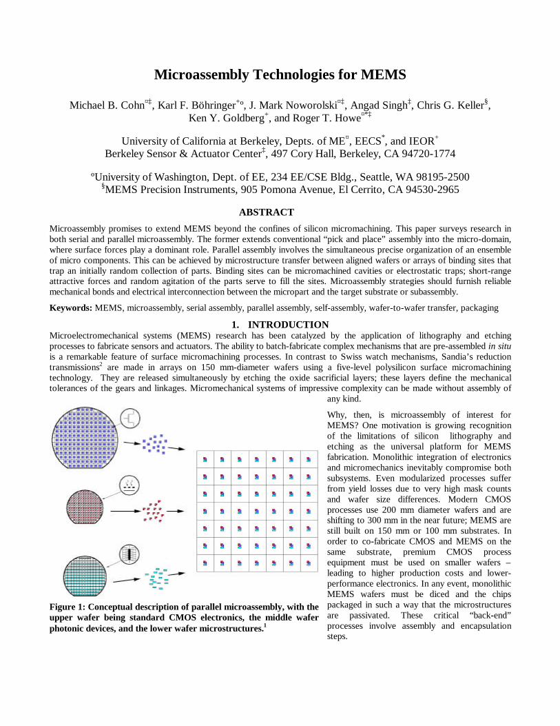
Figure 1: Conceptual description of parallel microassembly, with theupper wafer being standard CMOS electronics, the middle waferphotonic devices, and the lower wafer microstructures.1
Currently, microassembly is mandatory for sub-cm-scale microsystems that incorporate LEDs or diode lasers and siliconmicrostructures. Material incompatibilities impede co-fabrication of micro-opto-electro-mechanical systems (MOEMS).Figure 1 presents a conceptual vision of microassembly: microstructures, microelectronics, and optical elements areharvested from their respective substrates and distributed on a target substrate with micron-scale precision.
Microassembly is also required for the “pop-up hinges” used to build three-dimensional structures from surface-micromachined thin films.3 The interface between the existing cm-scale mechanical world and MEMS is another motivationfor developing microassembly processes. Finally, electronic packaging technology is not directly applicable to creatingmechanical or fluidic “feedthroughs” to microsystems. Inevitably, “some assembly is required” for any real-world MEMSapplication.
This paper surveys recent research in microassembly, beginning with serial methods, or “micro pick and place.”Micromachining techniques can furnish both manipulators and assembly pallets for organizing microparts. In order to pick upand release microparts, however, the scaling of physical forces must be carefully considered. Conventionally microfabricatedelements can sometimes be designed with the ability to either assemble by self-actuation upon release or by means ofelectrical actuation. The major research thrust, however, has targeted parallel processes that enable large numbers of parts tobe assembled simultaneously with micron-scale precision. These processes are categorized as either deterministic orstochastic, depending on whether the microparts are initially organized. Impressive results have been achieved in the past fewyears using both approaches. Deterministic parallel assembly has similarities to the rapidly evolving chip-scale packagingtechnologies, but concerns microstructure-on-substrate placement rather than chip-on-board assembly. Stochastic or self-assembly processes are being applied successfully to fabrication of LCD substrates with embedded silicon electronics. Thetraps for the microparts in this case are wells etched in the glass substrate. Chemical and electrostatic energy wells are alsouseful for trapping microparts. All types of microassembly require processes that bond the micropart to the substrate afterassembly. Finally, we assess the implications for MEMS of recent progress in microassembly.
2. SERIAL MICROASSEMBLYEfficient microassembly of parts less than 100 µm in size requires an infrastructure of microtools and microparts designed tointerface with each other and, ultimately, with the macroscopic world. The same rules of kinematic fixturing used in themacro world must be applied to the micro world; however, new constraints and phenomena must be taken into account. It ismore difficult to make the desired shapes with the necessary tolerances given the technology of micromachining availabletoday. For example, the verticality of sidewalls and the ratio of the magnitude of irregularities to the total size of the part aremuch poorer than for conventionally fabricated macroscopic parts. Design for assembly is a well-known concept inmanufacturing: the assembly process of an aggregate product is streamlined by a clever design of its components (forexample, if all componentscan be assembled withoutmoving or rotating thesubstrate). This concept iseven more important at themicro scale.
For microassembly, therelative importance of theforces that operate is verydifferent from that in themacro world. Gravity isusually negligible, whilesurface adhesion andelectrostatic forcesdominate4,5. This importanttopic is discussed later in thissection.
2.1. Recent Research in Serial MicroassemblyOne possible approach to microassembly is to improve the performance of conventional automated assembly systems.Commercial robotic systems with resolution and repeatability of a few microns are available (e.g.; from MRSI inChelmsford, Mass. or from Sysmelec in Switzerland). Even higher precision prototype systems have been described byQuaid and Hollis,6 Zesch,7 and Dual,8 among others, who use stepping motors and inertial drives to obtain sub-micrometermotion resolution. However, this approach requires increasingly sophisticated technology.
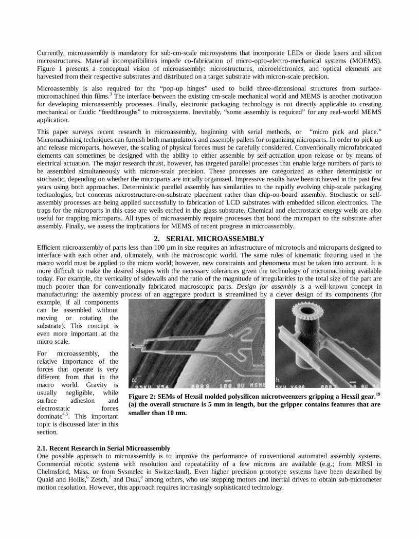
Figure 2: SEMs of Hexsil molded polysilicon microtweenzers gripping a Hexsil gear.19
(a) the overall structure is 5 mm in length, but the gripper contains features that aresmaller than 10 µm.
It has been observed that smaller parts require larger machines to handle them (and microscopic parts require hugemachines). Therefore, there is now increased interest in MEMS assembly tools that are at the same scale as the parts to beassembled. Micromachining processes have been used to fabricate a micro air table for parts handling.9 Residual stressgradients are the basis for “self-adjusting” structures that self-actuate to reduce critical dimensions upon release from thesubstrate.10 Hinged polysilicon structures are being applied to fabricate microoptical components; in some cases these structures have been observed to assembledue to turbulence in a rinse bath.11 Assembly is also feasible by means of integralactuators (either comb-drive or scratch-drive), combined with ohmic heating to fixthe structure in its assembled position. 12 Recently, Gonzaléz and co-workers at UCDavis have reported a suite of microfixturing and assembly concepts(“MicroJoinery") that uses microfabricated dovetail joints for easy precisionassembly.13
Microassembly can require unconventional approaches to the pick-and-placeparadigm. For example, Arai and Fukuda have built manipulators with heatedmicro holes.14 When the holes cool, they act as suction cups whose lower pressureholds appropriately shaped objects in place. Heating of the cavities increases thepressure and causes the objects to detach from the manipulator. The surface tensionof low viscosity fluids has been used to pick and center micro parts.15 Langen hasintroduced techniques for achieving precision machining and assembly in the samemachine tool, through use of self-alignment.16
Tweezers with integrated actuators and force sensors are a fundamental tool forteleoperated assembly of systems made up of independently microfabricated parts.Optical tweezers are widely used to manipulate bacteria, cells, and latexmicrospheres. There are many diverse niches requiring different microgrippersConventional machining done with high precision on millimeter scale parts (e.g.,Bartels Mikrotechnik GmbH, Germany) has produced working milliscale tweezers.Thermally actuated single crystal silicon micro-grippers have been fabricated bybulk etching.17 Electrostatically actuated polysilicon microgrippers have been usedto handle bacteria.18 Ultimately, the diversity in microgripper designs should rivalthat found in biology.
High aspect molded polysilicon (HexSil) processes are suitable for makingmicrotweezers.19 An initial demonstration of a micro pick and place task has beenperformed on surface micromachined oxide beams. HexSil tweezers are mm-scaleinstruments that are removed from the wafer they were made on and are mountedon conventional positioning systems; they are suitable for handling parts from afew µm to 1000 µm in size. The resulting assembly system provides a mechanicalinterface between the macro world and the micro world, with appropriatedimensions and stiffnesses at each end (Figure 2).
2.2. AdhesionModels based on classical mechanics and geometry are often used to describe small and micro scale robotics. However, thereare severe limitations to this approach. Due to scaling effects, forces that are insignificant at the macro scale becomedominant at the micro scale (and vice versa).20 For example, when parts to be handled are less than one millimeter in size,adhesive forces between gripper and object can be significant compared to gravitational forces. These adhesive forces ariseprimarily from surface tension, van der Waals, and electrostatic attractions and can be a fundamental limitation to parthandling. While it is possible to fabricate miniature versions of conventional robot grippers (Figure 2b), overcoming adhesioneffects for the smallest parts will be difficult.
The adhesion of particles to substrates has received substantial attention for problems such as particulate contamination insemiconductor manufacturing.21 Recent developments in MEMS, disk drives, and microassembly have stimulated the studyof friction effects at the micron scale. The normal Coulomb friction effects seen at the macro scale are quite different at themicron scale, since unpassivated surfaces exhibit large adhesive components. To grip microparts and then attach them to theworkpiece in the desired orientation, it is essential that a hierarchy of adhesive forces be established. Electrostatic forces dueto surface charges or ions in the ambient must be minimized. Adhesion of the micro part to the unclamped gripper surfaces(with zero applied force) should be less than the adhesion of the micro part to the substrate, to allow precise positioning of
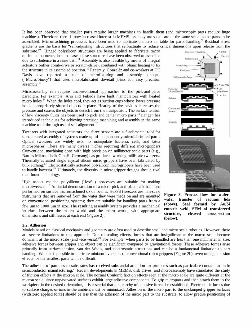
Figure 3. Process flow for wafer-wafer transfer of vacuum lids(above). Seal formed by Au/Sieutectic weld. SEM of transferredstructure, cleaved cross-section(below).
the part in the gripper. In order to release the part, the target spot on the workpiece must have a surface coating that providessufficiently strong adhesion to exceed that between the micro part and the unclamped gripper.4 The recent use of surfacetension as a means to grip micro parts is an interesting application of this particularly strong force in the micro domain.
3. PARALLEL MICROASSEMBLYThe throughput of serial microassembly is limited by the number of micromanipulators in the array and their bandwidth.Given that microfabrication processes can yieldmillions of devices, it is intriguing to considerwhether large ensembles of microparts can beassembled simultaneously. This class ofmicroassembly is termed “parallel.” There are twobasic approaches, one based on the massivelyparallel transfer between wafers of arrays ofmicrocomponents (deterministic parallelmicroassembly) and one utilizing various approachesto orient an initially random array of microparts(stochastic parallel microassembly.) These topicswill be considered in separate subsections.
3.1. Deterministic Parallel MicroassemblyDeterministic parallel microassembly refers to direct, wafer-to-wafer transfer of microstructures. Since the placement of thestructures is predetermined by their layout on the donor wafer, the challenge lies in bonding structures to the target. Theprocess is analogous to rubber-stamp printing, with pre-fabricated microstructures taking the place of the ink. While otherstructure-transfer processes have been demonstrated, wafer-wafer transfer isdistinguished by two key features: compatibility and throughput.
Compatibility with existing CMOS and MEMS processes is highly desirable. Anideal process would allow devices to be transferred to or from standard foundrywafers without requiring any “back-end” modifications. Other approaches, suchas epitaxial lift-off (ELO22) and Lucent’s SEED23 include a substrate removalstep, which is time-consuming and creates difficulties associated with handlingunsupported device layers. Use of an intermediate substrate addresses thisproblem and facilitates alignment.24 Ultimately, a transfer process sufficientlyfast to allow step-and-repeat transfer – akin to lithography – would have a majorimpact on MEMS technology.
The initial demonstration of wafer-to-wafer transfer involved vacuummicropackaging.25 Shells are fabricated on a handle wafer using the Hexsilprocess,19 and transferred over resonators. The seal is based on a Au/Si eutecticsolder joint. As shown in Figure 3, a typical structure has a top-hat cross-section,with stiffening ribs on the “roof.” The metallization on the target substrate maybe Au or, if thermo-compression bonding is employed, aluminum. The sealedpackages tolerate external pressures in excess of 1,000 PSI.
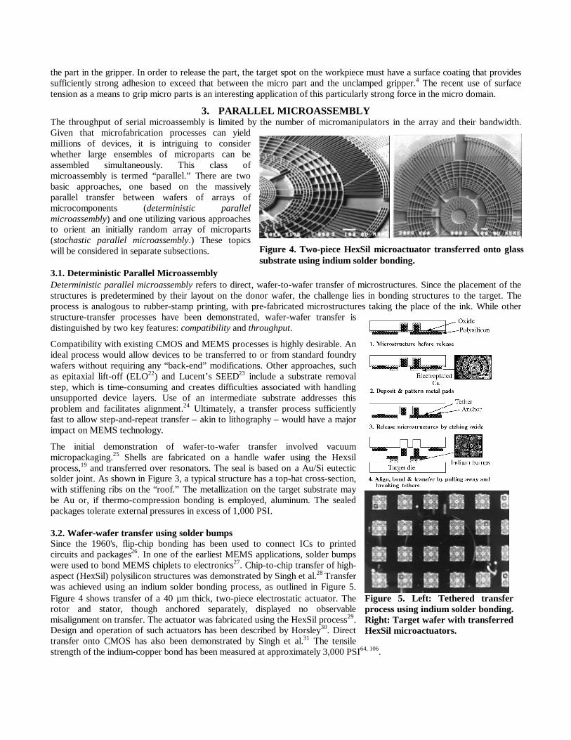
3.2. Wafer-wafer transfer using solder bumpsSince the 1960's, flip-chip bonding has been used to connect ICs to printedcircuits and packages26. In one of the earliest MEMS applications, solder bumpswere used to bond MEMS chiplets to electronics27. Chip-to-chip transfer of high-aspect (HexSil) polysilicon structures was demonstrated by Singh et al.28 Transferwas achieved using an indium solder bonding process, as outlined in Figure 5.Figure 4 shows transfer of a 40 µm thick, two-piece electrostatic actuator. Therotor and stator, though anchored separately, displayed no observablemisalignment on transfer. The actuator was fabricated using the HexSil process29.Design and operation of such actuators has been described by Horsley30. Directtransfer onto CMOS has also been demonstrated by Singh et al.31 The tensilestrength of the indium-copper bond has been measured at approximately 3,000 PSI64, 106.
Figure 4. Two-piece HexSil microactuator transferred onto glasssubstrate using indium solder bonding.
Figure 5. Left: Tethered transferprocess using indium solder bonding.Right: Target wafer with transferredHexSil microactuators.
Wafer-scale transfer of HexSil microactuators was demonstrated by Singh et al.32 Figure 5 shows a portion of the target waferwith transferred actuators. Since most of the failures appear to be due to bump non-uniformity, increase in yield is expectedwith optimization of the electroplating and bonding processes.
4. STOCHASTIC MICROASSEMBLY
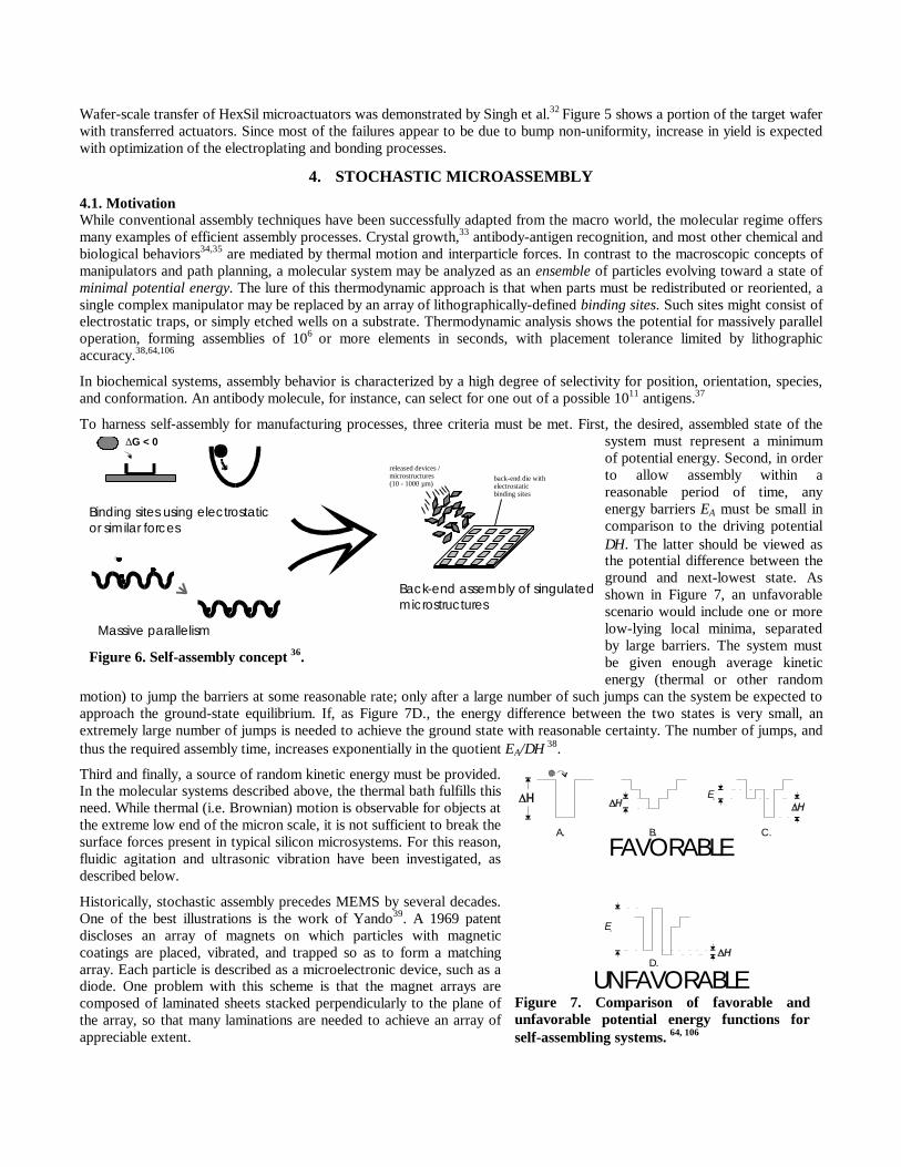
4.1. MotivationWhile conventional assembly techniques have been successfully adapted from the macro world, the molecular regime offersmany examples of efficient assembly processes. Crystal growth,33 antibody-antigen recognition, and most other chemical andbiological behaviors34,35 are mediated by thermal motion and interparticle forces. In contrast to the macroscopic concepts ofmanipulators and path planning, a molecular system may be analyzed as an ensemble of particles evolving toward a state ofminimal potential energy. The lure of this thermodynamic approach is that when parts must be redistributed or reoriented, asingle complex manipulator may be replaced by an array of lithographically-defined binding sites. Such sites might consist ofelectrostatic traps, or simply etched wells on a substrate. Thermodynamic analysis shows the potential for massively paralleloperation, forming assemblies of 106 or more elements in seconds, with placement tolerance limited by lithographicaccuracy.38,64,106
In biochemical systems, assembly behavior is characterized by a high degree of selectivity for position, orientation, species,and conformation. An antibody molecule, for instance, can select for one out of a possible 1011 antigens.37
To harness self-assembly for manufacturing processes, three criteria must be met. First, the desired, assembled state of thesystem must represent a minimumof potential energy. Second, in orderto allow assembly within areasonable period of time, anyenergy barriers EA must be small incomparison to the driving potential∆H. The latter should be viewed asthe potential difference between theground and next-lowest state. Asshown in Figure 7, an unfavorablescenario would include one or morelow-lying local minima, separatedby large barriers. The system mustbe given enough average kineticenergy (thermal or other random
motion) to jump the barriers at some reasonable rate; only after a large number of such jumps can the system be expected toapproach the ground-state equilibrium. If, as Figure 7D., the energy difference between the two states is very small, anextremely large number of jumps is needed to achieve the ground state with reasonable certainty. The number of jumps, andthus the required assembly time, increases exponentially in the quotient EA/∆H 38.
Third and finally, a source of random kinetic energy must be provided.In the molecular systems described above, the thermal bath fulfills thisneed. While thermal (i.e. Brownian) motion is observable for objects atthe extreme low end of the micron scale, it is not sufficient to break thesurface forces present in typical silicon microsystems. For this reason,fluidic agitation and ultrasonic vibration have been investigated, asdescribed below.
Historically, stochastic assembly precedes MEMS by several decades.One of the best illustrations is the work of Yando39. A 1969 patentdiscloses an array of magnets on which particles with magneticcoatings are placed, vibrated, and trapped so as to form a matchingarray. Each particle is described as a microelectronic device, such as adiode. One problem with this scheme is that the magnet arrays arecomposed of laminated sheets stacked perpendicularly to the plane ofthe array, so that many laminations are needed to achieve an array ofappreciable extent.
released devices / microstructures (10 - 1000 µm)
back-end die with electrostatic binding sites
∆G < 0
Binding sites using electrostatic or similar forces
Massive parallelism
Back-end assembly of singulatedmicrostructures
Figure 6. Self-assembly concept 36.
EA
EA
FAVORABLE
UNFAVORABLE
A. B. C.
D.
Figure 7. Comparison of favorable andunfavorable potential energy functions forself-assembling systems. 64, 106
The APOS parts feeder is described by Hitakawa40. The feeder uses an array of “berths” cut into a vibrating plate. Parts arefed over the plate, and the berths are designed, like the track of the bowl feeder, to accept only parts in a given orientation.Eventually, all the berths are filled. Similar techniques have been described for creating pin-grid arrays and connectors.
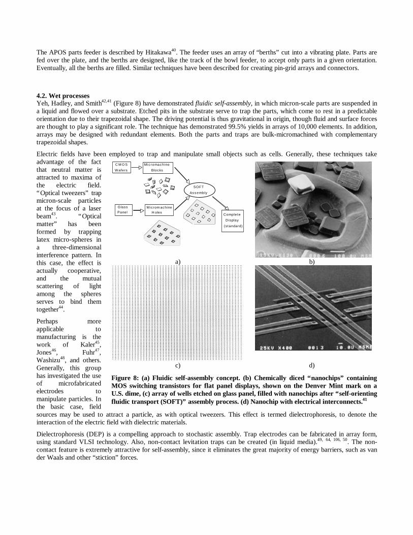
4.2. Wet processesYeh, Hadley, and Smith42,41 (Figure 8) have demonstrated fluidic self-assembly, in which micron-scale parts are suspended ina liquid and flowed over a substrate. Etched pits in the substrate serve to trap the parts, which come to rest in a predictableorientation due to their trapezoidal shape. The driving potential is thus gravitational in origin, though fluid and surface forcesare thought to play a significant role. The technique has demonstrated 99.5% yields in arrays of 10,000 elements. In addition,arrays may be designed with redundant elements. Both the parts and traps are bulk-micromachined with complementarytrapezoidal shapes.
Electric fields have been employed to trap and manipulate small objects such as cells. Generally, these techniques takeadvantage of the factthat neutral matter isattracted to maxima ofthe electric field.“Optical tweezers” trapmicron-scale particlesat the focus of a laserbeam43. “Opticalmatter” has beenformed by trappinglatex micro-spheres ina three-dimensionalinterference pattern. Inthis case, the effect isactually cooperative,and the mutualscattering of lightamong the spheresserves to bind themtogether44.
Perhaps moreapplicable tomanufacturing is thework of Kaler45,Jones46, Fuhr47,Washizu48, and others.Generally, this grouphas investigated the useof microfabricatedelectrodes tomanipulate particles. Inthe basic case, fieldsources may be used to attract a particle, as with optical tweezers. This effect is termed dielectrophoresis, to denote theinteraction of the electric field with dielectric materials.
Dielectrophoresis (DEP) is a compelling approach to stochastic assembly. Trap electrodes can be fabricated in array form,using standard VLSI technology. Also, non-contact levitation traps can be created (in liquid media).49, 64, 106, 50. The non-contact feature is extremely attractive for self-assembly, since it eliminates the great majority of energy barriers, such as vander Waals and other “stiction” forces.
C M O S
Wafers
Micromachine
Blocks
SOFT
Assemb ly
GlassPanel
M icrom achineH oles Comp le te
Display
(standard)
a) b)
c) d)
Figure 8: (a) Fluidic self-assembly concept. (b) Chemically diced “nanochips” containingMOS switching transistors for flat panel displays, shown on the Denver Mint mark on aU.S. dime, (c) array of wells etched on glass panel, filled with nanochips after “self-orientingfluidic transport (SOFT)” assembly process. (d) Nanochip with electrical interconnects.41
Whitesides52 has described several molecular self-assembling systems. Forexample, an “ink” composed of a self-assembling molecular monolayer hasbeen demonstrated for lithographic pattern transfer, using a rubber stamp toachieve 0.1 µm resolution. Self-assembly of millimeter-scale, three-dimensional objects has also been demonstrated by the same group53, and wasalso described by Cohn54. In this case, hydrophobically coated surfaces ofsmall parts suspended in an aqueous medium come together when the parts areagitated.
4.3. Dry processesIn 1991, Cohn, Kim, and Pisano described stochastic assembly using vibrationand gravitational forces to assemble arrays of up to 1000 silicon chiplets38.
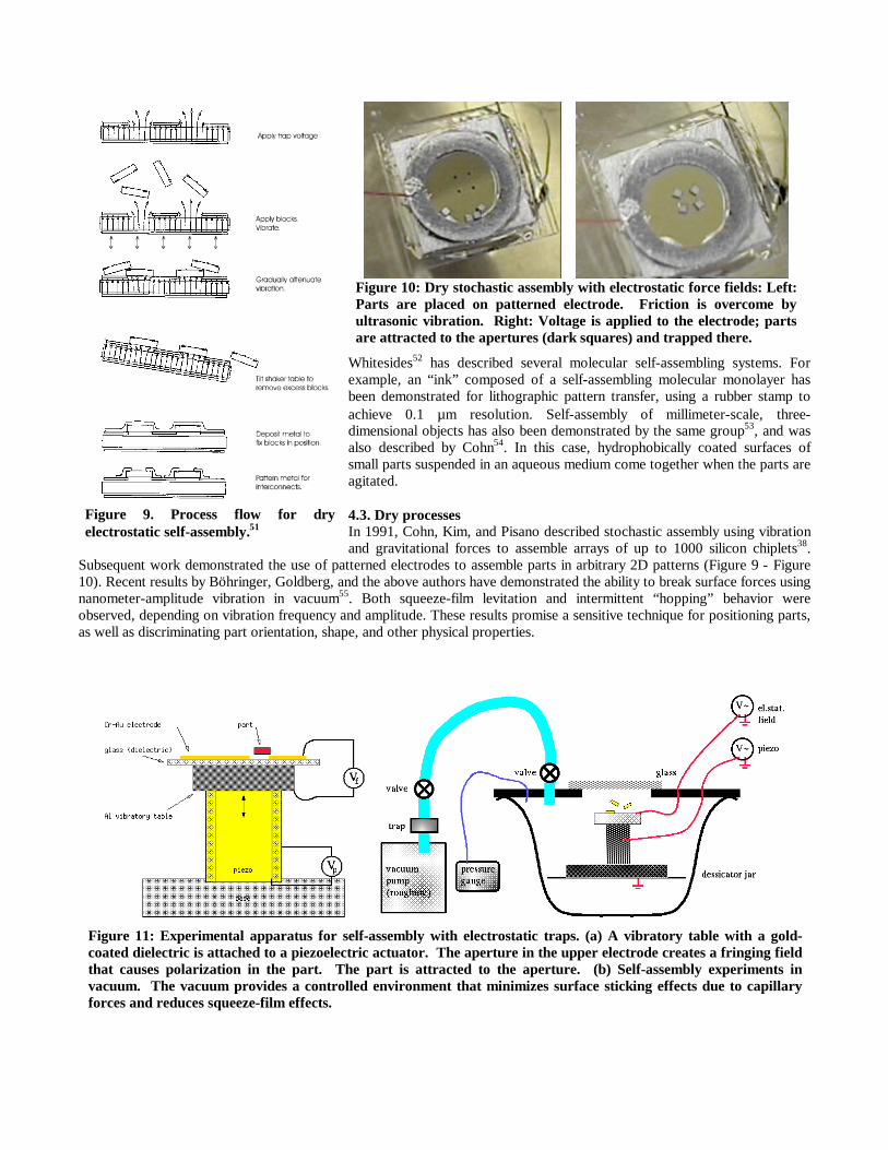
Subsequent work demonstrated the use of patterned electrodes to assemble parts in arbitrary 2D patterns (Figure 9 - Figure10). Recent results by Böhringer, Goldberg, and the above authors have demonstrated the ability to break surface forces usingnanometer-amplitude vibration in vacuum55. Both squeeze-film levitation and intermittent “hopping” behavior wereobserved, depending on vibration frequency and amplitude. These results promise a sensitive technique for positioning parts,as well as discriminating part orientation, shape, and other physical properties.
Figure 9. Process flow for dryelectrostatic self-assembly.51
Figure 10: Dry stochastic assembly with electrostatic force fields: Left:Parts are placed on patterned electrode. Friction is overcome byultrasonic vibration. Right: Voltage is applied to the electrode; partsare attracted to the apertures (dark squares) and trapped there.
Figure 11: Experimental apparatus for self-assembly with electrostatic traps. (a) A vibratory table with a gold-coated dielectric is attached to a piezoelectric actuator. The aperture in the upper electrode creates a fringing fieldthat causes polarization in the part. The part is attracted to the aperture. (b) Self-assembly experiments invacuum. The vacuum provides a controlled environment that minimizes surface sticking effects due to capillaryforces and reduces squeeze-film effects.
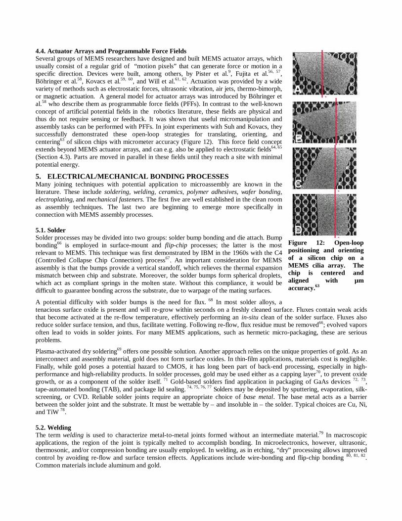
4.4. Actuator Arrays and Programmable Force FieldsSeveral groups of MEMS researchers have designed and built MEMS actuator arrays, whichusually consist of a regular grid of “motion pixels” that can generate force or motion in aspecific direction. Devices were built, among others, by Pister et al.9, Fujita et al.56, 57,Böhringer et al.58, Kovacs et al.59, 60, and Will et al.61, 62. Actuation was provided by a widevariety of methods such as electrostatic forces, ultrasonic vibration, air jets, thermobimorph,or magnetic actuation. A general model for actuator arrays was introduced by Böhringer etal.58 who describe them as programmable force fields (PFFs). In contrast to the wellknownconcept of artificial potential fields in the robotics literature, these fields are physical andthus do not require sensing or feedback. It was shown that useful micromanipulation andassembly tasks can be performed with PFFs. In joint experiments with Suh and Kovacs, theysuccessfully demonstrated these openloop strategies for translating, orienting, andcentering63 of silicon chips with micrometer accuracy (Figure 12). This force field conceptextends beyond MEMS actuator arrays, and can e.g. also be applied to electrostatic fields64, 65
(Section 4.3). Parts are moved in parallel in these fields until they reach a site with minimalpotential energy.
5. ELECTRICAL/MECHANICAL BONDING PROCESSESMany joining techniques with potential application to microassembly are known in theliterature. These include soldering, welding, ceramics, polymer adhesives, wafer bonding,electroplating, and mechanical fasteners. The first five are well established in the clean roomas assembly techniques. The last two are beginning to emerge more specifically inconnection with MEMS assembly processes.
5.1. SolderSolder processes may be divided into two groups: solder bump bonding and die attach. Bumpbonding66 is employed in surface-mount and flip-chip processes; the latter is the mostrelevant to MEMS. This technique was first demonstrated by IBM in the 1960s with the C4(Controlled Collapse Chip Connection) process67. An important consideration for MEMSassembly is that the bumps provide a vertical standoff, which relieves the thermal expansionmismatch between chip and substrate. Moreover, the solder bumps form spherical droplets,which act as compliant springs in the molten state. Without this compliance, it would bedifficult to guarantee bonding across the substrate, due to warpage of the mating surfaces.
A potential difficulty with solder bumps is the need for flux. 68 In most solder alloys, atenacious surface oxide is present and will re-grow within seconds on a freshly cleaned surface. Fluxes contain weak acidsthat become activated at the re-flow temperature, effectively performing an in-situ clean of the solder surface. Fluxes alsoreduce solder surface tension, and thus, facilitate wetting. Following re-flow, flux residue must be removed66; evolved vaporsoften lead to voids in solder joints. For many MEMS applications, such as hermetic micro-packaging, these are seriousproblems.
Plasma-activated dry soldering69 offers one possible solution. Another approach relies on the unique properties of gold. As aninterconnect and assembly material, gold does not form surface oxides. In thin-film applications, materials cost is negligible.Finally, while gold poses a potential hazard to CMOS, it has long been part of back-end processing, especially in high-performance and high-reliability products. In solder processes, gold may be used either as a capping layer70, to prevent oxidegrowth, or as a component of the solder itself. 71 Gold-based solders find application in packaging of GaAs devices 72, 73,tape-automated bonding (TAB), and package lid sealing. 74, 75, 76, 77 Solders may be deposited by sputtering, evaporation, silk-screening, or CVD. Reliable solder joints require an appropriate choice of base metal. The base metal acts as a barrierbetween the solder joint and the substrate. It must be wettable by – and insoluble in – the solder. Typical choices are Cu, Ni,and TiW 78.
5.2. WeldingThe term welding is used to characterize metal-to-metal joints formed without an intermediate material.79 In macroscopicapplications, the region of the joint is typically melted to accomplish bonding. In microelectronics, however, ultrasonic,thermosonic, and/or compression bonding are usually employed. In welding, as in etching, “dry” processing allows improvedcontrol by avoiding re-flow and surface tension effects. Applications include wire-bonding and flip-chip bonding 80, 81, 82.Common materials include aluminum and gold.
Figure 12: Open-looppositioning and orientingof a silicon chip on aMEMS cilia array. Thechip is centered andaligned with µmaccuracy.63
Welding, in the more conventional sense, has been demonstrated in MEMS applications by Fedder.83 Aluminum tethers weremelted and reflowed by ohmic heating. The surface tension forces were used to assemble and actuate polysilicon structures.One problem with this approach is that the welds could not actually be used to join two objects that were initially separate.Moreover, due to the high current requirements, it was difficult to parallelize more than four welds in a single circuit.
Finally, a tack-welding technique has been demonstrated by Cohn64,106 using evaporated metals, solders, and ceramics. Theadvantage of this technique is that vacuum-deposited materials are highly reactive, bonding to metals, oxides, and othermaterials. The substrate temperature need not rise above ambient. Moreover, the deposition is capable of bridging a gap,providing tolerance for substrate non-planarity. This is a potential approach for assembly of fragile or complex structures,such as stacked HexSil. Bartek has demonstrated a similar technique, using aluminum deposition to seal a polysilicon micro-cavity 84.
5.3. CeramicsNon-metal-based techniques have also been demonstrated. Glass frits consist of a low-melting glass powder in a resin binder,which may be applied by silk-screen. Typical applications include ceramic-to-metal joints and hermetic packaging.85
Limitations include resolution and hermeticity, as well as relatively high re-flow temperatures (usually > 300°C for high-quality materials). Current MEMS applications include hermetic packaging of microsensors.
Hermetic encapsulation of microstructures by surface micromachining techniques has been demonstrated by several researchgroups. In this case, a micro-shell is fabricated and sealed by high-temperature deposition of thin films.86,87,88,89,90
5.4. Polymer adhesivesPolymer adhesives are also used for flip-chip type interconnection, whether as a component of solder fluxes or pastes, or Z-axis conductive adhesives 91,92. UV-curable adhesives are seeing increased use in wafer bonding and epitaxial lift-offapplications93. However, adhesives may be difficult to pattern and may have undesirable characteristics such as high vaporpressure, limited temperature tolerance, and low modulus. An advantage, however, is adhesion to a wide range of materials,such as metals, ceramics, and other polymer. Solid polymer films may be laminated conformally over microstructures forplanarization of high-aspect topography, or to provide enclosed fluidic channels. Recently, autoclavable packaging has beendemonstrated using polymer materials.
5.5. Wafer bondingInterest in wafer bonding for micromachining applications dates to the work of Lasky 94 and Shimbo 95. Schmidt 96 andFarrens 97 provide reviews and bibliographies relevant to MEMS. Principal wafer bonding methods include anodic bondingand fusion bonding. Initially, anodic silicon-to-glass bonding predominated, though more recently GaAs-Si, Si-Si, and Si-SiNbonding have been demonstrated.98 Applications of wafer bonding have been in the production of SOI wafers, power devices,and MEMS such as pressure sensors. With the increased application of deep-trench RIE to MEMS 99, exotic multi-layer SOIsubstrates are expected to become more prevalent.
In the area of microstructure-level assembly, however, wafer bonding displays several limitations. Primarily, since thebonding mechanism is van der Waals bonding, the substrates must be brought very close together – preferably less than 1 nm– so particulates, roughness, and wafer curvature must be carefully controlled. A single micron-sized particulate can lead tocm-sized bond defects.100 Farrens has reported that handling of wafers with metal tweezers can lead to bond defects. Wafersmust meet stringent criteria for overall roughness and curvature to assure successful bonding. Initially, wafer bonding wasconfined to high temperatures, e.g. 800-1000°C. Recently, however, processes have been demonstrated at 300°C, and evenroom temperature.101 The mechanical performance of these bonds is expected to be excellent, since there are no adhesive orbonding materials used that may exhibit creep.
5.6. ElectroplatingAside from its application to solder bump deposition described above, electroplating can be used directly to join two piecesof material. Wise describes the mechanical and electrical interconnection of a 3D neural probe structure 102. The advantage ofthis technique is that the deposition is defined by lithographically fabricated features on the 2D components. Following theinitial lithography, there are no precision assembly steps. Electroless processes may also be employed, avoiding the need tomake electrical contact to the workpieces. Electroplating requires a cathode connection to the intended deposition surface,which may not be practical when there are multiple, complex, or electrically discontinuous structures. Electroless platingsimply requires an appropriate metallic seed surface, such as gold, copper, nickel, or platinum. Kim has recentlydemonstrated the use of electroplated nickel plugs or “rivets” to join two bulk silicon structures 103.
Increased use of plating techniques is expected in the microassemblyarea. Other than standard sputter or evaporation apparatus for seedlayer deposition, no special equipment is required. Moreover,deposition is selective and may be masked. Perhaps the only limitationof the technique lies in the area of vacuum packaging – there is no
obvious way to form an evacuated cavity, as might be done by vacuum deposition. Also, materials deposited by electro- orelectroless plating tend to out-gas over time. In addition, it may be more difficult to apply these techniques for selectivebonding; spatial control would seem more easily achieved in a heat- or pressure-driven process.
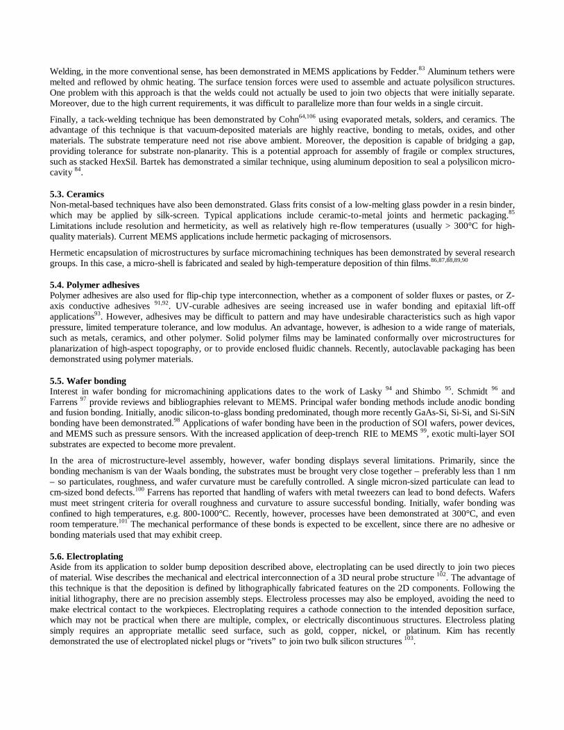
5.7. Mechanical FastenersMicromechanical fasteners include Reed’s “micro Velcro”104 as well as the snap fastener demonstrated by Prasad andBöhringer105. These are intriguing in that they avoid the problems of thermal cycling, surface wettability, and other materialscompatibility problems inherent in welding processes. At the same time, they afford the potential for self-alignment and, inthe case of the snap fastener, integrated actuation. Cohn has described a “shear-lock” transfer mechanism106, based on thesnap fastener, allowing self-aligned wafer-wafer transfer of individual microstructures. The shear-lock mechanism useslaterally-engaging barbs, in conjunction with break-away tethers. The barbs cold-weld to pylons on the target wafer,providing electromechanical interconnection. This mechanism offers sub-micron alignment precision, using non-precisionequipment and relatively low aspect-ratio micromachining.
6. CONCLUSIONSExtending MEMS beyond the confines of IC-based processes will inevitably involve some form of assembly. An earlyapplication of microassembly may be the placement of microstructures onto CMOS substrates, followed by theirencapsulation with transferred package lids. Such “batch assembled” MEMSmay include inertial sensors and RF signal processing elements; theirperformance may equal that of their monolithic counterparts, since unmodified,state-of-the-art CMOS electronics can be used. In contrast to traditional hybrids,parasitics in microassembled MEMS could be comparable to those seen inmonolithic equivalents. Microphotonics or MOEMS is another “technologydriver” since a monolithic solution is impractical due to materialsincompatiblility between photonic devices and micromechanical mirrors andmechanisms.
Serial assembly using micro pick and place has been demonstrated in thelaboratory, in some cases using MEMS micromanipulators. In order for serialprocesses to have a commercial impact, large arrays of manipulators andassociated control algorithms are needed. By micromachining its keycomponents, it may prove feasible to make a cost effective “micro assembly line”for MEMS and other applications. Further research is needed into the control andexploitation of the relatively large surface tension and electrostatic forcesencountered in micro parts handling.
Parallel assembly processes are generally less mature. However, they have thegreatest potential for fundamentally changing MEMS and other microfabricationtechnologies. If microparts can be “batch assembled” on substrates with veryhigh yields, parallel assembly may become an alternative to conventional
Figure 13: Single-crystal silicon snap fastener.105
Coarsealignment
Shear toengagebarbs
Shear tobreaktethers
Self-alignment
Figure 14. Shear-lock mechanism.
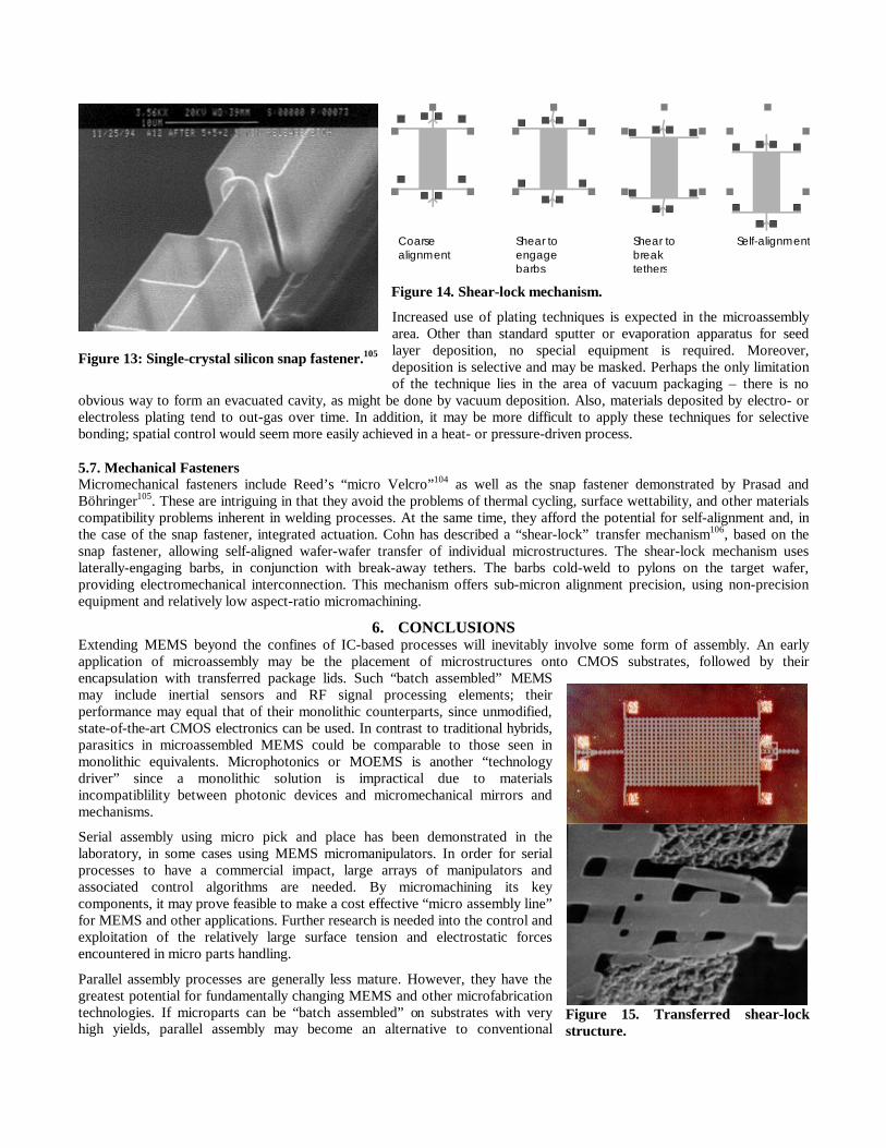
Figure 15. Transferred shear-lockstructure.
lithography and etching. Deterministic parallel assembly strategies involve the transfer of microstructures from a donor waferto a target wafer. Initial research has focussed on using metal-based bonds to make electrical and mechanical contact betweenthe donated microstructure and the substrate. This approach draws on the large body of knowledge in solder bumps for flip-chip attachment. Much additional study is needed to develop a variety of bonding processes, with adhesive-less bondinglikely to demand careful surface preparation. Yields and the limits to precision of wafer-to-wafer transfer processes using fullwafers have yet to be established, but initial results are promising using compression bonding. The tolerance to waferwarpage is a primary question that remains to be resolved.
Stochastic parallel assembly is a rich area for research, with various systems being investigated in both dry and liquidambients. With proper design of the trapping mechanism and the microparticles, theory predicts that high assembly yields arefeasible for ensembles with 107 or more elements. The fluid-based assembly of silicon “nanochips” into glass wells withetched particle traps has demonstrated yields of higher than 99.5%. Micromachining plays a key role in this process, since thechemical dicing of the silicon CMOS substrate is necessary for formation of the nanonchips, in addition to the preciseshaping of the holes in the glass substrate. Successful assembly of large arrays is yet to be demonstrated for the case ofvibrationally excited dry micropart ensembles with electrostatic particle traps. Tighter control of the surface properties of themicroparts and the substrate is likely to improve the reproducibility of this process.
Given the rapid progress of microassembly technology over the past five years, it is quite plausible that it will soon bemaking an impact in MEMS manufacturing. Regardless of the particular assembly strategy used, the implication is that dense“quasi-monolithic” microsystems will be much easier to realize. One fallout is that integration of MEMS with electronics in amerged, monolithic process sequence will not be as compelling for many applications. Further in the future, microassemblyprocesses will likely prove instrumental in the development of 3D microsystems.
7. ACKNOWLEDGMENTSWe are grateful to Dr. Mark A. Hadley of Beckmen Display, Inc., Berkeley, California for supplying graphics on self-orienting fluidic transport assembly. Research in microassembly has been supported by BSAC, an NSF Industry/UniversityCooperative Research Center, DARPA, Electronics Technology Office through contract DABT 63-95-C0028 and subcontractSRA-10737797 to Raytheon (Dr. Thomas R. Schimert, PI). In addition, research in the IEOR Dept. at Berkeley on assemblyhas been supported in part by an NSF grant on Challenges in CISE: Planning and Control for Massively ParallelManipulation (CDA-9726389), an NSF CISE Postdoctoral Associateship in Experimental Computer Science to Karl F.Böhringer (CDA-9705022), and an NSF Presidential Faculty Fellowship to Ken Goldberg (IRI-9553197).
8. REFERENCES 1 K. F. Böhringer, K. Goldberg, M. Cohn, R. Howe, and A. Pisano, “Parallel microassembly with electrostatic force fields,”
Int. Conf. on Robotics and Automation, Leuven, Belgium, May 1998. Figure after M. B. Cohn, “Self assembly usingelectrostatic particle traps,” Ph.D. Qualifying Exam, Dept. of EECS, Univ. of Calif. at Berkeley, May 1995.
2 S. M. Rodgers and J. J. Sniegowski, “5-level polysilicon surface micromachine technology: application to complexmechanical systems,” Solid State Sensor and Actuator Workshop, Hilton Head, S.C., June 1998, pp.144-149.
3 Pister, K.S.J.; Judy, M.W.; Burgett, S.R.; Fearing, R.S. Microfabricated hinges. Sensors and Actuators A (Physical),vol.A33, (no.3), June 1992. p.249-56.
4 R. S. Fearing, “A survey of sticking effects for micro parts handling,” IEEE/RSJ Int. Workshop on Intelligent Robots andSystems, Pittsburgh, Penn., 1995.
5 C. G. Keller and R. T. Howe, “Hexsil tweezers for teleoperated microassembly,” IEEE Micro Electro Mechanical SystemsWorkshop, Nagoya, Japan, Jan. 1997, pp. 72-77.
6 A. E. Quaid and R. L. Hollis. Cooperative 2-dof robots for precision assembly. IEEE Int. Conf. on Robotics andAutomation, Minneapolis, Minn., Apr. 1996.
7 W. Zesch. Multi-Degree-of-Freedom Micropositioning Using Stepping Principles. PhD Thesis, Swiss Federal Institute ofTechnology, Zurich, Switzerland, 1997.
8 G. Danuser, I. Pappas, B. Vögeli, W. Zesch, and J. Dual. “Manipulation of microscopic objects with nanometer precision:Potentials and limitations in nano-robot design,” submitted to Int. Journal of Robotics Research, 1997.
9 K. S. J. Pister, R. S. Fearing, and R. T. Howe, “A planar air levitated electrostatic actuator system,” IEEE Micro ElectroMechanical Systems Workshop, Napa Valley, Calif., Feb. 1990, pp. 67-71.
10 M. W. Judy, Y.-H. Cho, R. T. Howe, and A. P. Pisano, “Self-adjusting microstructures (SAMS),” ,” IEEE Micro ElectroMechanical Systems Workshop, Nara, Japan, Jan.-Feb. 1991, pp. 51-56.
11 K. S. J. Pister, M. W. Judy, S. R. Burgett, and R. S. Fearing, “Microfabricated hinges: 1mm vertical features with surface
micromachining,” 6th Int. Conf. on Solid-State Sensors and Actuators, San Francisco, Calif., June 1991.12 Y. Fukuta, D. Collard, T. Akiyama, E. H. Yang, and H. Fujita, “Microactuated self-assembling of 3D polysilicon structures
with reshaping technology,” IEEE Micro Electro Mechanical Systems Workshop, Nagoya, Japan, Jan. 1997, pp. 477-481.13 C. Gonzaléz, R. L. Smith, D. G. Howitt, and S. D. Collins, “MicroJoinery: concept, definition, and application to
microsystem development,” Sensors and Actuators A (Physical), 66, 315-332 (1998).14 F. Arai and T. Fukuda, “A new pick up and release method by heating for micromanipulation, IEEE Micro Electro
Mechanical Systems Workshop, Nagoya, Japan, Jan. 1997, pp. 383-388.15 C. Bark, T. Binnenböse, G. Vögele, T. Weisener, and M. Widmann, “Gripping with low viscosity fluids,” IEEE Micro
Electro Mechanical Systems Workshop, Heidelberg, Germany, Feb. 1998, pp. 301-305.16 H. H. Langen, “A study on micromachining/assembly,” Ph.D. thesis, Univ. of Tokyo, 1994.17 W.-H. Chu and M. Mehregany, “Microfabricated tweezer with a large gripping force and a large range of motion,” Solid
State Sensor and Actuator Workshop, Hilton Head, S.C., June 1994, pp. 107-111.18 C.-J. Kim, R. S. Muller, A. P. Pisano, and M. G. Lim, “Polysilicon microtweezers,” Sensors and Actuators A (Physical),
33, 221-227 (1992).19 C. G. Keller, “Microfabricated silicon high aspect ratio flexures for in-plane motion”, Ph.D. Thesis, Dept. of Materials
Science and Mineral Engineering, Univ. of Calif. at Berkeley, 1998.20 I. Shimoyama, “Scaling in microrobotics,” IEEE/RSJ Int. Workshop on Intelligent Robots and Systems, Pittsburgh, Penn.,
1995, pp. 208-211.21 R. A. Bowling, “A theoretical review of particle adhesion,” in K. L. Mittal, ed., Particles on Surfaces I Detection,
Adhesion, and Removal. New York: Plenum, pp. 129-155.22 E. T. Yablonovitch, J.P. Harbison,; R. Bhat, “Extreme selectivity in the lift-off of epitaxial GaAs films.” Applied Physics
Letters, 51, 28 Dec. 1987, pp .2222-4.23 K. W. Goosen, et al, “GaAs MQW modulators integrated with silicon CMOS,” IEEE Photonics Tech. Lett., 7, 360-363
(1995).24 Camperi-Ginestet, C.; Hargis, M.; Jokerst, N.M.; Allen, M., "Alignable epitaxial liftoff of GaAs materials with selective
deposition using polyimide diaphragms," IEEE Photonics Technology Letters, vol.3, no.12 p.1123-6 Dec. 1991.25 M.B. Cohn, Y.-C. Liang, R.T. Howe, A.P. Pisano, “wafer-to-wafer transfer of microstructures for vacuum packaging,”
1996 Solid-State Sensor and Actuator Workshop, Hilton Head Island, SC, USA, June 2-6, 1996.26 L.S. Goodman, “Geometric optimization of controlled collapse interconnections,” IBM J. Res. Devel 13(3): pp. 251-265,
1969.27 K.W. Marcus, V. Dhuler, D. Roberson, A. Cowen, M. Berry, S. Nangalia, “Smart MEMS: Flip Chip Integration of MEMS
and Electronics,” SPIE Smart Materials Conference, Feb 1995.28 A. Singh, D.A. Horsley, M.B. Cohn, A.P. Pisano, R.T. Howe, “Batch Transfer of Microstructures using flip-chip solderbump bonding”, Technical Digest, Transducers'97, Chicago, June, 1997.29 C.G. Keller and M. Ferrari, “Milli-Scale Polysilicon Structures,” Solid-State Sensor and Actuator Workshop, Hilton Head
SC, pp. 132-137, June 1994.30 D.A. Horsley, A. Singh, A.P. Pisano, R. Horowitz, “Angular Micropositioners for Disk Drives,” Intl. Workshop on Micro
Electro Mechanical Systems, Nagoya, Japan, pp. 454-459, 1997.31 Horsley D.A.; Cohn, M.B.; Singh, A.; Horowitz, R.; Pisano, A.P. Design and fabrication of an angular microactuator for
magnetic disk drives. Journal of Microelectromechanical Systems, vol.7, (no.2), IEEE, June 1998. p.141-8.32 A. Singh, D.A. Horsley, M.B. Cohn, A.P. Pisano, R.T. Howe, “Batch Transfer of Microstructures using flip-chip solder
bonding”, in the Journal of Microelectromechanical Systems submitted 5/98.33 S. Wolf and R. N. Tauber, Silicon Processing for the VLSI Era, Volume 1: Process Technology, Lattice Press, Sunset
Beach, CA, 1986, p. 8 ff.34 J. Darnell, H. Lodish, D. Baltimore, Molecular cell biology / New York: W.H. Freeman, 1986.35 C. Cantor, The behavior of biological macromolecules / San Francisco : W. H. Freeman, 1980.36. M. B. Cohn, R. S. Fearing “Self-Assembly in Microfabrication,” Seminar Presented to the Berkeley Sensor and Actuator
Center, Nov. 22, 1992.37 H. Lodish, D. Baltimore, A. Berk, S Zipursky, P. Matsudaira, J. Darnell, Molecular Cell Biology, Third Edition, / New
York: W. H. Freeman, 1995, p. 1322.38 M. Cohn, C. J. Kim, A.P. Pisano, “Self-Assembling Electrical Networks: An Application of Micromachining Technology,”
Transducers ’91 International Conference on Solid-State Sensors and Actuators, Digest of Technical Papers, SanFrancisco, June 24-27, 1991 / New York: IEEE, 1991, p. 493.
39 S. Yando, Method and Apparatus for Fabricating an Array of Discrete Elements, U.S. Patent No. 3,439,416, Assigned to
GTE Laboratories, Inc., 1969.40 H. Hitakawa. “Advanced parts orientation system has wide application,” Assembly Automation, 8(3), 1988.41 M. A. Hadley, “Self-orienting fluidic transport (SOFT) assembly of liquid crystal displays,” presentation at the Defense
Manufacturing Conference, Palm Springs, Calif., Dec, 1-4, 1997.42 H. J. Yeh, J.S. Smith, “Fluidic self-assembly of microstructures and its application to the integration of GaAs on Si,”
Proceedings IEEE Micro Electro Mechanical Systems, Oiso, Japan, 25-28 Jan 1994 / New York: IEEE, 1994. p.279-84.43 A. Ashkin and J.M. Dziedzic, Science 235, 1517 (1987).44 M. M. Burns, J. M. Fournier, J. A. Golovchenko, “Optical Binding,” Physical Review Letters 63:12, p. 1233 ff. (18 Sept
1989).45 K.V.I.S. Kaler and H.A. Pohl, “Dynamic dielectrophoretic levitation of living individual cells,” IEEE Trans. IAS, vol. IA-
19, 1983, 1089-1093.46 T.B. Jones, Electromechanics of Particles / New York: Cambridge University Press, 1995.47 G.Fuhr, W.M. Arnold, R. Hagedorn, T. Muller, W. Benecke, B. Wagner, and U. Zimmermann, “Levitation, holding, and
rotation of cells within traps made by high-frequency fields,” Biochim. Biophys. Acta, 1108, 1992, 215-22348 M. Washizu, T.B. Jones, and K.V.I.S. Kaler, “Higher-order DEP effects: Levitation at a field null,” Biochim. Biophys.
Acta, 1158, 1993a, 40-46.49 T.B. Jones and J.P. Kraybill, “Active feedback-controlled dielectrophoretic levitation,” J. Appl. Phys., 60, 1986, 1247-
1252.50 M.B. Cohn, R. T. Howe, A. P. Pisano, “Self-Assembly of Microsystems Using Non-Contact Electrostatic Traps,” Proc.
ASME International Mechanical Engineering Congress and Exposition (IMECE), San Francisco, California (November1995), p. 893-900.
51 Cohn, M.B., "Self Assembly of Microfabricated Devices," US Patent No. 5,355,577, October, 1994.52 Berggren, K.K.; Bard, A. Wilbur, J.L.; Gillaspy, J.D.; Helg, A.G.; McClelland, J.J.; Rolston, S.L.; Phillips, W.D.; Prentiss,
M.; Whitesides, G. M. “Microlithography by using neutral metastable atoms and self-assembled monolayers.” Sciencev269, n5228 (Sept 1, 1995):1255
53 A. Terfort, N. Bowden, and G.M. Whitesides, “Three-dimensional self-assembly of millimetre-scale components.” Nature386, 6621 (March 13, 1997):162.
54 M. Cohn, U.S. Patent No. 5,355,577, issued 10/1994.55 K.-F. Böhringer, M. Cohn, K. Y. Goldberg, R. Howe, A. Pisano, Electrostatic Self-Assembly Aided by Ultrasonic
Vibration, Presented at AVS'97 - American Vacuum Society National Symposium on Micro Electro Mechanical Systems(MEMS) , San Jose, CA (October 1997).
56 H. Fujita. Group work of microactuators. In International Advanced Robot Program Workshop on MicromachineTechnologies and Systems, pages 24--31, Tokyo, Japan, Oct. 1993.
57 S. Konishi and H. Fujita. A conveyance system using air flow based on the concept of distributed micro motion systems.In Transducers --- Digest Int. Conf. on SolidState Sensors and Actuators, pages 28--31, Pacifico, Yokohama, Japan, June1993.
58 K.F. Böhringer, B. R. Donald, R. Mihailovich, and N. C. MacDonald. A theory of manipulation and control formicrofabricated actuator arrays. In Proc. IEEE Workshop on Micro Electro Mechanical Systems (MEMS), pages 102--107, Oiso, Japan, Jan. 1994.
59 C. W. Storment, D. A. Borkholder, V. Westerlind, J. W. Suh, N. I. Maluf, and G. T. A. Kovacs. Flexible, dryreleasedprocess for aluminum electrostatic actuators. Journal of Microelectromechanical Systems, 3(3):90--96, Sept. 94.
60 J. W. Suh, S. F. Glander, R. B. Darling, C. W. Storment, and G. T. A. Kovacs. Combined organic thermal and electrostaticomnidirectional ciliary microactuator array for object positioning and inspection. In Proc. Solid State Sensor andActuator Workshop, Hilton Head, NC, June 1996.
61 C. Liu, T. Tsao, P. Will, Y. Tai, and W. Liu. A micromachined magnetic actuator array for microrobotics assemblysystems. In Transducers --- Digest Int. Conf. on SolidState Sensors and Actuators, Stockholm, Sweden, June 1995.
62 W. Liu and P. Will. Parts manipulation on an intelligent motion surface. In IEEE/RSJ Int. Workshop on Intelligent Robots& Systems (IROS), Pittsburgh, PA, 1995
63 K.F. Böhringer, B. R. Donald, N. C. MacDonald, G. T. A. Kovacs, and J. W. Suh. Computational methods for design andcontrol of MEMS micromanipulator arrays. IEEE Computer Science and Engineering, pages 17--29, January--March1997.
64 M. B. Cohn. Assembly Techniques for Microelectromechanical Systems. Ph.D. thesis, University of California at Berkeley,Department of Electrical Engineering and Computer Sciences, 1997.
65 K.F. Böhringer, K. Goldberg, M. B. Cohn, R. Howe, and A. Pisano. Parallel microassembly with electrostatic force fields.In Proc. IEEE Int. Conf. on Robotics and Automation (ICRA), Leuven, Belgium, May 1998.66. J. S. Hwang,. Modern solder technology for competitive electronics / New York: McGraw-Hill, 1996.67. L.S. Goodman, “Geometric optimization of controlled collapse interconnections,” IBM J. Res. Devel 13(3): pp. 251-265,
196968. M. M. Schwartz, “Fundamentals of Soldering,” in ASM Handbook, 10th Edition, Volume 6: Welding, Brazing, and
Soldering / Materials Park, OH; ASM International, 1990, p. 129-30.69. S. M. Bobbio, N. G. Koopman, S. Nangalia, Fluxless soldering sample pretreating system, U.S. Patent No. 5,499,754,
MCNC Corporation, Research Triangle Park, NC. ISSUED: Mar. 19, 199670. Y. C. Chen, C. Y. Wang, and C. C. Lee, “Directly deposited lead-indium-gold composite solder,” IEEE Transactions on
Components, Hybrids, and Manufacturing Technology, vol.16, (no.8), Dec. 1993. p.789-93.71. T. Nishikawa, M. Ijuin, R. Satoh, Y. Iwata, M. Tamura, M. Shirai, “Fluxless soldering process technology,” 1994
Proceedings. 44th Electronic Components and Technology Conference, Washington, DC, USA, 1-4 May 1994 / NewYork, NY, USA: IEEE, 1994. p.286-92.
72. C. H. Lee, Y. M. Wong, C. Doherty, K.L. Tai, E. Lane, D. D. Bacon, F. Baiocchi, and A. Katz, “Study of Ni as a barriermetal in AuSn Soldering Application for Laser Chip/Submount Assembly, J. Appl. Phys. 72 (8), 10/15/1992, pp. 3808-15.
73. M.A. Hadley, Vertical-cavity surface-emitting laser diodes: design, growth, mode control and integration by fluidic self-assembly, Ph.D. thesis, EECS Dept., UC Berkeley, 1994.
74. G. S. Matijasevic, C. C. Lee, C. Y. Wang, “Au-Sn phase diagram and properties related to its use as a bonding medium,”Thin Solid Films, 223 (1993), 276-87.
75. T. Kawanobe, K. Miyamoto, M. Hirano, Proc. 33rd IEEE Electronic Components and Technology Conf., 1983, IEEE, NewYork, 1983, pp. 221-26.
76. W. H. Ko, J. T. Suminto, G. J. Yeh, in C. D. Fung, P.W. Cheung, W.H. Ko, and D.G. Fleming (eds.) Micromachining andMicropackaging of Transducers, Elsevier, Amsterdam, 1985, pp. 41-61.
77. C.A. Mackay and S.W. Levine, IEEE Trans. Compon., Hybrids, Manuf. Technol., 9 (1986) pp. 195-201.78. C.H. Lee, Y.M. Wong, C. Doherty, K.L. Tai et al, “Study of Ni as a barrier metal in AuSn soldering application for laser
chip / submount assembly,” J. Appl. Phys. 72:8 (15 Oct 1992), pp. 3808-15.79. American Welding Society. Welding handbook, Charlotte Weisman, editor. 7th ed. Miami, Fla.: American Welding
Society, 1984.80. R.R. Tummala, E. J. Rumaszewski, A.G. Klopfenstein, Microelectronics Packaging Handbook. Technology Drivers. Part
1, Chapman & Hill, 1997.81. H. Yatsuda and T. Eimura, “Flip-chip assembly technique of SAW devices,” 1995 International Symposium on
Microelectronics, Los Angeles, CA, USA, 24-26 Oct. 1995.) SPIE, 1995. p.365-70.82 D. Gupta, “Evaluation of alternative processes for Au-Sn-Au flip chip bonding of power devices. 1995 International
Symposium on Microelectronics, Los Angeles, CA, USA, 24- Oct. 1995.) SPIE, 1995. p.371-7.83. G.K.Fedder, J.C. Chang, R.T. Howe, “Thermal assembly of polysilicon microactuators with narrow-gap electrostatic comb
drive,” Technical Digest. IEEE Solid-State Sensor and Actuator Workshop, Hilton Head Island, SC, USA, 22-25 June1992, New York, NY, USA: IEEE, 1992. p.63-8.
84 Bartek, M.; Foerster, J.A.; Wolffenbuttel, R.F. Vacuum sealing of microcavities using metal evaporation. Sensors andActuators A (Physical), vol.A61, (no.1-3), (EUROSENSORS X, Leuven, Belgium, 8-11 Sept. 1996.) Elsevier, June 1997.p.364-8.
85. Ajluni, C. Silicon accelerometer targets airbag restraint systems. Electronic Design, vol.43, (no.21), 13 Oct. 1995. p.143-4.(Motorola MMAS40G accelerometer with glass frit hermetic package)
86 K. Ikeda, et al, “Three dimensional micromachining of silicon resonant strain gauge, 7th Sensor Symposium, Tokyo, Japan,May 1988, pp. 193-196.
87 C. H. Mastrangelo and R. S. Muller, Int. Electron Devices Meeting, San Francisco, Calif., Dec. 1989, pp. 503-506.88 Guckel, H.; Rypstat, C.; Nesnidal, M.; Zook, J.D.; Burns, D.W.; Arch, D.K. Polysilicon resonant microbeam technology
for high performance sensor applications. Technical Digest. IEEE Solid-State Sensor and Actuator Workshop, HiltonHead Island, SC, USA, 22-25 June 1992. New York, NY, USA: IEEE, 1992. p.153-6.
89 Lin, L., McNair, K.M., Howe, R.T., and Pisano, A.P., “Vacuum Encapsulated Lateral Microresonators,” Digest ofTransducers ’93, International Conference on Solid-State Sensors and Actuators, pp. 270-3, 1993.
90 K. S. Leibouitz, A. P. Pisano, and R. T. Howe, “Permeable polysilicon etch-access windows for microshell fabrication,” 8th
Int. Conf. on Solid-State Sensors and Actuators, Stockholm, Sweden, June 1995, vol. 1, pp. 224-227.91. Alpha Metals, Advanced Products Division, Jersey City, NJ. Alpha-Bond anisotropically conductive film preliminary data
sheet. 10/94.92. P. H. Singer, “Die bonding and package sealing materials,” Trans. on Electron Dev., ED-26, 12, pp. 1896-1905 (1979).93. Norland Products, Inc., New Brunswick, NJ (908)545-7828.94. J.B. Lasky, S. R. Stiffler, F.R. White, J. R. Abernathey, “Silicon-on-insulator (SOI) by bonding and etch-back,” Technical
Digest, 1985 IEEE International Electron Devices Meeting, p. 684, Dec 1985.95. M. Shimbo, K. Furukawa, K. Fukuda, T. Tanzawa, “Silicon-to-silicon direct bonding method,” Journal Of Applied
Physics, Vol. 60, No. 8, P. 2987, Oct 1986.96. M. A. Schmidt, “Silicon wafer bonding for micromechancal devices,” Solid-State Sensor and Actuator Workshop, Hilton
Head, SC, June 13-16, 1994, pp. 127-131.97. J. A. Folta, C. E. Hunt, S. N. Farrens, “Low-temperature wafer bonding of surfaces using a reactive sputtered oxide,”
Journal of the Electrochemical Society, vol. 141, (no.8), Aug. 1994. pp. 2157 - 60.98. R.W. Bower, M. S. Ismail, and B. E. Roberd, “Low temperature Si3N4 direct bonding,” Appl. Phys. Lett., vol. 62, no. 26,
pp. 3485-7, 1993.99. T.J. Brosnihan, J.M. Bustillo, A.P. Pisano, R.T. Howe, “Embedded interconnect and electrical isolation for high-aspect-
ratio, SOI inertial instruments.” Tranducers 97. 1997 International Conference on Solid-State Sensors and Actuators.Chicago, IL, USA, 16-19 June 1997. New York, NY, USA: IEEE, 1997. p. 637-40 vol. 1.
100. Q.-Y. Tong, U. Gosele, “Semiconductor wafer bonding: recent developments.” Materials Chemistry and Physics, vol.37,(no.2), March 1994. p.101-27.
101. Q. Y. Tong, G. Cha, R. Gafiteanu, U. Gosele, “Low Temperature Wafer Direct Bonding,” Journal ofMicroelectromechanical Systems, vol. 3, no. 1 (March 1994), pp. 29-35.
102. Hoogerwerf, A.C., Wise, K.D., “A three-dimensional neural recording array,” Transducers ’91 1991 InternationalConference on Solid-State Sensors and Actuators, San Francisco, CA, 24-27 June, 1991, pp. 120-123.
103. B. Shivkumar and C.-J. Kim "Microriveting - A New Wafer Joining Method" IEEE Micro Electro Mechanical SystemsWorkshop, Nagoya, Japan, Jan. 1997,pp. 197-202.
104. H. Han, L.E. Weiss, M.L. Reed, “Design and Modeling of a Micromechanical Surface Bonding System,” Transducers’91, pp. 974-77.
105. R. Prasad, K.-F. Böhringer, N. C. MacDonald, “Design, Fabrication, and Characterization of SCS Latching SnapFasteners for Micro Assembly,” Proc. ASME International Mechanical Engineering Congress and Exposition (IMECE),San Francisco, California (November 1995).
106 M. B. Cohn, Assembly Techniques for Microelectromechanical Systems, Ph.D. Thesis, Department of ElectricalEngineering and Computer Science, University of California, Berkeley, 1997.