Embed Size (px)
Citation preview

MicroBlaze Debug Module (MDM) v3.2
LogiCORE IP Product Guide
Vivado Design Suite
PG115 April 4, 2018

MicroBlaze Debug Module v3.2 2PG115 April 4, 2018 www.xilinx.com
Table of ContentsIP Facts
Chapter 1: OverviewFeature Summary. . . . . . . . . . . . . . . . . . . . . . . . . . . . . . . . . . . . . . . . . . . . . . . . . . . . . . . . . . . . . . . . . . 6Licensing and Ordering . . . . . . . . . . . . . . . . . . . . . . . . . . . . . . . . . . . . . . . . . . . . . . . . . . . . . . . . . . . . . 6
Chapter 2: Product SpecificationStandards . . . . . . . . . . . . . . . . . . . . . . . . . . . . . . . . . . . . . . . . . . . . . . . . . . . . . . . . . . . . . . . . . . . . . . . . 7Performance and Resource Utilization. . . . . . . . . . . . . . . . . . . . . . . . . . . . . . . . . . . . . . . . . . . . . . . . . 7Port Descriptions . . . . . . . . . . . . . . . . . . . . . . . . . . . . . . . . . . . . . . . . . . . . . . . . . . . . . . . . . . . . . . . . . . 7Register Space . . . . . . . . . . . . . . . . . . . . . . . . . . . . . . . . . . . . . . . . . . . . . . . . . . . . . . . . . . . . . . . . . . . 13Trace Packet Definition . . . . . . . . . . . . . . . . . . . . . . . . . . . . . . . . . . . . . . . . . . . . . . . . . . . . . . . . . . . . 28
Chapter 3: Designing with the CoreGeneral Design Guidelines . . . . . . . . . . . . . . . . . . . . . . . . . . . . . . . . . . . . . . . . . . . . . . . . . . . . . . . . . 34Clocking. . . . . . . . . . . . . . . . . . . . . . . . . . . . . . . . . . . . . . . . . . . . . . . . . . . . . . . . . . . . . . . . . . . . . . . . . 35Resets . . . . . . . . . . . . . . . . . . . . . . . . . . . . . . . . . . . . . . . . . . . . . . . . . . . . . . . . . . . . . . . . . . . . . . . . . . 36Debug Register Access Sequence . . . . . . . . . . . . . . . . . . . . . . . . . . . . . . . . . . . . . . . . . . . . . . . . . . . . 36Cross Trigger Programming . . . . . . . . . . . . . . . . . . . . . . . . . . . . . . . . . . . . . . . . . . . . . . . . . . . . . . . . . 37External Trace Connection . . . . . . . . . . . . . . . . . . . . . . . . . . . . . . . . . . . . . . . . . . . . . . . . . . . . . . . . . 39Protocol Description . . . . . . . . . . . . . . . . . . . . . . . . . . . . . . . . . . . . . . . . . . . . . . . . . . . . . . . . . . . . . . 40
Chapter 4: Design Flow StepsCustomizing and Generating the Core . . . . . . . . . . . . . . . . . . . . . . . . . . . . . . . . . . . . . . . . . . . . . . . . 41Parameter Values. . . . . . . . . . . . . . . . . . . . . . . . . . . . . . . . . . . . . . . . . . . . . . . . . . . . . . . . . . . . . . . . . 43Constraining the Core . . . . . . . . . . . . . . . . . . . . . . . . . . . . . . . . . . . . . . . . . . . . . . . . . . . . . . . . . . . . . 46Simulation . . . . . . . . . . . . . . . . . . . . . . . . . . . . . . . . . . . . . . . . . . . . . . . . . . . . . . . . . . . . . . . . . . . . . . 47Synthesis and Implementation . . . . . . . . . . . . . . . . . . . . . . . . . . . . . . . . . . . . . . . . . . . . . . . . . . . . . . 47
Appendix A: UpgradingMigrating to the Vivado Design Suite. . . . . . . . . . . . . . . . . . . . . . . . . . . . . . . . . . . . . . . . . . . . . . . . . 48Upgrading in the Vivado Design Suite . . . . . . . . . . . . . . . . . . . . . . . . . . . . . . . . . . . . . . . . . . . . . . . . 48
Send Feedback
MicroBlaze Debug Module v3.2 3PG115 April 4, 2018 www.xilinx.com
Appendix B: DebuggingFinding Help on Xilinx.com . . . . . . . . . . . . . . . . . . . . . . . . . . . . . . . . . . . . . . . . . . . . . . . . . . . . . . . . . 49Debug Tools . . . . . . . . . . . . . . . . . . . . . . . . . . . . . . . . . . . . . . . . . . . . . . . . . . . . . . . . . . . . . . . . . . . . . 50Simulation Debug. . . . . . . . . . . . . . . . . . . . . . . . . . . . . . . . . . . . . . . . . . . . . . . . . . . . . . . . . . . . . . . . . 51Hardware Debug . . . . . . . . . . . . . . . . . . . . . . . . . . . . . . . . . . . . . . . . . . . . . . . . . . . . . . . . . . . . . . . . . 51AXI4-Lite Slave Interface Debug . . . . . . . . . . . . . . . . . . . . . . . . . . . . . . . . . . . . . . . . . . . . . . . . . . . . . 52
Appendix C: Application Software DevelopmentDevice Drivers . . . . . . . . . . . . . . . . . . . . . . . . . . . . . . . . . . . . . . . . . . . . . . . . . . . . . . . . . . . . . . . . . . . 53
Appendix D: Additional Resources and Legal NoticesXilinx Resources . . . . . . . . . . . . . . . . . . . . . . . . . . . . . . . . . . . . . . . . . . . . . . . . . . . . . . . . . . . . . . . . . . 54Documentation Navigator and Design Hubs . . . . . . . . . . . . . . . . . . . . . . . . . . . . . . . . . . . . . . . . . . . 54References . . . . . . . . . . . . . . . . . . . . . . . . . . . . . . . . . . . . . . . . . . . . . . . . . . . . . . . . . . . . . . . . . . . . . . 55Revision History . . . . . . . . . . . . . . . . . . . . . . . . . . . . . . . . . . . . . . . . . . . . . . . . . . . . . . . . . . . . . . . . . . 56Please Read: Important Legal Notices . . . . . . . . . . . . . . . . . . . . . . . . . . . . . . . . . . . . . . . . . . . . . . . . 57
Send Feedback

MicroBlaze Debug Module v3.2 4PG115 April 4, 2018 www.xilinx.com Product Specification
IntroductionThis document provides the design specification for the MicroBlaze™ Debug Module (MDM) core which enables JTAG-based debugging of one or more MicroBlaze processors. The MDM core is added separately in the Vivado Design Suite and connected to the MicroBlaze processors to be debugged.
Features• Support for JTAG-based software debug
tools
• Support for debugging up to 32 MicroBlaze processors
• Support for synchronized control of multiple MicroBlaze processors
• Support for a JTAG-based UART with a configurable AXI4-Lite interface
• Based on Boundary Scan (BSCAN) logic in Xilinx® devices
• Direct JTAG-based access to memory with a configurable AXI4 master interface
• Configurable software access to debug functionality through the AXI4-Lite interface
• Support for cross-trigger between connected MicroBlaze cores, Zynq-7000 Processing System and Integrated Logic Analyzer (ILA) cores
• External trace function to funnel program trace from connected MicroBlaze cores to external interfaces
• Connection to Debug Bridge through external BSCAN to support Xilinx Virtual Cable (XVC)
IP Facts
LogiCORE™ IP Facts Table
Core Specifics
Supported Device Family(1)
UltraScale+™UltraScale™
Zynq®-7000 All Programmable SoC7 Series
Supported User Interfaces AXI4, AXI4-Lite
Resources Performance and Resource Utilization web page
Provided with CoreDesign Files RTL
Example Design Not Provided
Test Bench Not Provided
Constraints File Not Provided
Simulation Model VHDL Behavioral
Supported S/W Driver(2) Standalone and Linux
Tested Design Tools(3)
Design Entry Tools Vivado® Design Suite
Simulation For supported simulators, see theXilinx Design Tools: Release Notes Guide
Synthesis Tools Vivado Synthesis
SupportProvided by Xilinx at the Xilinx Support web page
Notes: 1. For a complete listing of supported devices, see the Vivado IP
catalog.2. Standalone driver details can be found in the SDK directory
(<install_directory>/SDK/<release>/data/embeddedsw/doc//xilinx_drivers.htm). Linux OS and driver support information is available from the Xilinx Wiki page.
3. For the supported versions of the tools, see theXilinx Design Tools: Release Notes Guide.
Send Feedback

MicroBlaze Debug Module v3.2 5PG115 April 4, 2018 www.xilinx.com
Chapter 1
OverviewThe block diagram of the MicroBlaze™ Debug Module is shown in Figure 1-1.
X-Ref Target - Figure 1-1
Figure 1-1: MicroBlaze Debug Module (MDM) Core Block Diagram
MDEBUG_0
MDEBUG_31
LMB_0
LMB_31
Interrupt
S_AXI
External Trace
M_AXIS
M_AXI
.
.
.
.
.
.
.
.
.
.
.
.
XMTC
Trig Out
Trig In
ExternalBSCAN To
MicroBlaze
Send Feedback

MicroBlaze Debug Module v3.2 6PG115 April 4, 2018 www.xilinx.com
Chapter 1: Overview
Feature Summary• Enables JTAG-based debugging of one or more MicroBlaze processors.
• Instantiates one BSCAN primitive, or allows an external BSCAN to be used. In devices that contain more than one BSCAN primitive, the MDM core uses the USER2 BSCAN by default.
• External BSCAN also supports connection to the Debug Bridge LogiCORE™ IP, to use the Xilinx Virtual Cable (XVC) for debugging over non-JTAG interfaces.
• Includes a UART with a configurable slave bus interface which can be configured for an AXI4-Lite interconnect. The UART TX and RX signals are transmitted over the device JTAG port to and from the Xilinx® System Debugger (XSDB) tool. The UART behaves in a manner similar to the LogiCORE™ IP AXI (UART) Lite core.
• Provides a configurable AXI4 master port for direct access to memory from JTAG. This allows fast program download, as well as transparent memory access when the connected MicroBlaze processors are executing.
• Allows software to control debug and observe debug status through the AXI4-Lite slave interface. This is particularly useful for software performance measurements and analysis, using the MicroBlaze extended debug functionality for performance monitoring.
• Includes a cross-trigger capability, which enables routing of trigger events between connected MicroBlaze processors, as well as an external interface compatible with the Zynq-7000 Processing System.
• Includes support for external trace interfaces to funnel and store MicroBlaze program trace in external storage. Program trace from connected MicroBlaze processors can be directly output on an external interface, stored in external memory via the AXI4 master port, or transmitted on an AXI4-Stream interface compatible with the Zynq-7000 Processing System.
• Supports MicroBlaze parallel debug access, designed to provide faster direct access to MicroBlaze debug registers, and to improve timing compared to serial debug.
In general, it is recommended to only use this feature when software debug through JTAG is not required, because otherwise the MDM must perform a serial to parallel conversion of the JTAG signals, which requires additional logic.
Licensing and OrderingThis Xilinx® LogiCORE™ IP module is provided at no additional cost with the Xilinx Vivado® Design Suite under the terms of the Xilinx End User License. Information about this and other Xilinx LogiCORE IP modules is available at the Xilinx Intellectual Property page. For information about pricing and availability of other Xilinx LogiCORE IP modules and tools, contact your local Xilinx sales representative.
Send Feedback
MicroBlaze Debug Module v3.2 7PG115 April 4, 2018 www.xilinx.com
Chapter 2
Product Specification
StandardsThe MDM core adheres to the AMBA® AXI4 and AXI4-Lite Interface standard (see ARM® AMBA AXI and ACE Protocol Specification ARM IHI 0022E [Ref 1]).
The MDM core adheres to the AMBA AXI4-Stream Interface standard (see ARM AMBA AXI4-Stream Protocol Specification, Version 1.0 [Ref 2]).
Performance and Resource UtilizationFor details about performance and resource utilization, visit Performance and Resource Utilization.
Port DescriptionsThe I/O signals for the MDM core are listed and described in Tables 2-1 to 2-12.
Table 2-1: System Signals
Signal Name Interface I/O InitialState Description
Interrupt O 0 Interrupt from UART
Debug_SYS_Rst O 0 Debug system reset
Ext_BRK O 0 External break
Ext_NM_BRK O 0 External non-maskable break
Send Feedback

MicroBlaze Debug Module v3.2 8PG115 April 4, 2018 www.xilinx.com
Chapter 2: Product Specification
Table 2-2: AXI4-Lite Slave Interface Signals (C_DBG_REG_ACCESS = 1)
Signal Name Interface I/O InitialState Description
S_AXI_ACLK
S_AXI
I - AXI Clock
S_AXI_ARESETN I - AXI Reset, active-Low
S_AXI_AWADDR[C_S_AXI_ADDR_WIDTH-1:0] I - Write Address
S_AXI_AWVALID I - Write Address Valid
S_AXI_AWREADY O 0 Write Address Ready
S_AXI_WDATA[C_S_AXI_DATA_WIDTH-1:0] I - Write Data
S_AXI_WSTB[C_S_AXI_DATA_WIDTH/8-1:0] I - Write Strobes
S_AXI_WVALID I - Write Valid
S_AXI_WREADY O 0 Write Ready
S_AXI_BRESP[1:0] O 0x0 Write Response
S_AXI_BVALID O 0 Write Response Valid
S_AXI_BREADY I - Write Response Ready
S_AXI_ARADDR[C_S_AXI_ADDR_WIDTH-1:0] I - Read Address
S_AXI_ARVALID I - Read Address Valid
S_AXI_ARREADY O 0 Read Address Ready
S_AXI_RDATA[C_S_AXI_DATA_WIDTH-1:0] I - Read Data
S_AXI_RRESP[1:0] O 0x0 Read Response
S_AXI_RVALID O 0 Read Valid
S_AXI_RREADY I - Read Ready
Table 2-3: AXI4 Master Interface Signals (C_DBG_MEM_ACCESS = 1 or C_TRACE_OUTPUT = 3)
Signal Name Interface I/O InitialState Description
M_AXI_ACLK
M_AXI
I - AXI Clock
M_AXI_ARESETN I - AXI Reset, active-Low
M_AXI_AWID[C_M_AXI_THREAD_ID_WIDTH-1:0] O 0x0 Write Address ID
M_AXI_AWADDR[C_M_AXI_ADDR_WIDTH-1:0] O 0x0 Write Address
M_AXI_AWLEN[7:0] O 0x0 Write Address Length
M_AXI_AWSIZE[2:0] O 0x2 Write Address Size
M_AXI_AWBURST[1:0] O 0x1 Write Address Burst
M_AXI_AWLOCK O 0 Write Address Lock
M_AXI_AWCACHE[3:0] O 0x3 Write Address Cache
M_AXI_AWPROT[2:0] O 0x2 Write Address Protection
M_AXI_AWQOS[3:0] O 0x0 Write Address QoS
M_AXI_AWVALID O 0 Write Address Valid
M_AXI_AWREADY I - Write Address Ready
Send Feedback

MicroBlaze Debug Module v3.2 9PG115 April 4, 2018 www.xilinx.com
Chapter 2: Product Specification
M_AXI_WDATA[C_M_AXI_DATA_WIDTH-1:0]
M_AXI
O 0x0 Write Data
M_AXI_WSTRB[C_M_AXI_DATA_WIDTH/8-1:0] O 0x0 Write Strobes
M_AXI_WLAST O 0 Write Last
M_AXI_WVALID O 0 Write Valid
M_AXI_WREADY I - Write Ready
M_AXI_BRESP[1:0] I - Write Response
M_AXI_BID[C_M_AXI_THREAD_ID_WIDTH-1:0] I - Write Response ID
M_AXI_BVALID I - Write Response Valid
M_AXI_BREADY O 0 Write Response Ready
M_AXI_ARID[C_M_AXI_THREAD_ID_WIDTH-1:0] O 0x0 Read Address ID
M_AXI_ARADDR[C_M_AXI_ADDR_WIDTH-1:0] O 0x0 Read Address
M_AXI_ARLEN[7:0] O 0x0 Read Address Length
M_AXI_ARSIZE[2:0] O 0x0 Read Address Size
M_AXI_ARBURST[1:0] O 0x1 Read Address Burst
M_AXI_ARLOCK O 0 Read Address Lock
M_AXI_ARCACHE[3:0] O 0x3 Read Address Cache
M_AXI_ARPROT[2:0] O 0x2 Read Address Protection
M_AXI_ARQOS[3:0] O 0x0 Read Address QoS
M_AXI_ARVALID O 0 Read Address Valid
M_AXI_ARREADY I - Read Address Ready
M_AXI_RID[C_M_AXI_THREAD_ID_WIDTH-1:0] I - Read ID
M_AXI_RDATA[C_M_AXI_DATA_WIDTH-1:0] I - Read Data
M_AXI_RRESP[1:0] I - Read Response
M_AXI_RLAST I - Read Last
M_AXI_RVALID I - Read Valid
M_AXI_RREADY O 0 Read Ready
Table 2-4: LMB Master Interface Signals (C_DBG_MEM_ACCESS = 1, n = 0–31)
Signal Name Interface I/O InitialState Description
LMB_Data_Addr_n[0:C_DATA_SIZE-1]
LMB_n
O 0x0 Data Address
LMB_Data_Read_n[0:C_DATA_SIZE-1] I - Data Read Bus
LMB_Data_Write_n[0:C_DATA_SIZE-1] O 0x0 Data Write Bus
LMB_Addr_Strobe_n O 0 Address Strobe
LMB_Read_Strobe_n O 0 Read Strobe
LMB_Write_Strobe_n O 0 Write Strobe
LMB_Ready_n I - Ready
Table 2-3: AXI4 Master Interface Signals (C_DBG_MEM_ACCESS = 1 or C_TRACE_OUTPUT = 3)
Signal Name Interface I/O InitialState Description
Send Feedback
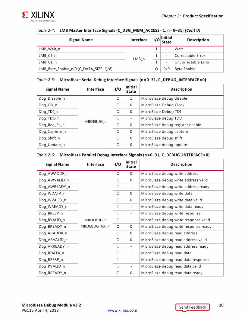
MicroBlaze Debug Module v3.2 10PG115 April 4, 2018 www.xilinx.com
Chapter 2: Product Specification
LMB_Wait_n
LMB_n
I - Wait
LMB_CE_n I - Correctable Error
LMB_UE_n I - Uncorrectable Error
LMB_Byte_Enable_n[0:(C_DATA_SIZE-1)/8] O 0x0 Byte Enable
Table 2-5: MicroBlaze Serial Debug Interface Signals (n = 0–31, C_DEBUG_INTERFACE = 0)
Signal Name Interface I/O InitialState Description
Dbg_Disable_n
MBDEBUG_n
O 1 MicroBlaze debug disable
Dbg_Clk_n O 0 MicroBlaze Debug Clock
Dbg_TDI_n O 0 MicroBlaze Debug TDI
Dbg_TDO_n I - MicroBlaze debug TDO
Dbg_Reg_En_n O 0 MicroBlaze debug register enable
Dbg_Capture_n O 0 MicroBlaze debug capture
Dbg_Shift_n O 0 MicroBlaze debug shift
Dbg_Update_n O 0 MicroBlaze debug update
Table 2-6: MicroBlaze Parallel Debug Interface Signals (n = 0–31, C_DEBUG_INTERFACE > 0)
Signal Name Interface I/O InitialState Description
Dbg_AWADDR_n
MBDEBUG_n
MBDEBUG_AXI_n
O 0 MicroBlaze debug write address
Dbg_AWVALID_n O 0 MicroBlaze debug write address valid
Dbg_AWREADY_n I - MicroBlaze debug write address ready
Dbg_WDATA_n O 0 MicroBlaze debug write data
Dbg_WVALID_n O 0 MicroBlaze debug write data valid
Dbg_WREADY_n I - MicroBlaze debug write data ready
Dbg_BRESP_n I - MicroBlaze debug write response
Dbg_BVALID_n I - MicroBlaze debug write response valid
Dbg_BREADY_n O 0 MicroBlaze debug write response ready
Dbg_ARADDR_n O 0 MicroBlaze debug read address
Dbg_ARVALID_n O 0 MicroBlaze debug read address valid
Dbg_ARREADY_n I - MicroBlaze debug read address ready
Dbg_RDATA_n I - MicroBlaze debug read data
Dbg_RRESP_n I - MicroBlaze debug read data response
Dbg_RVALID_n I - MicroBlaze debug read data valid
Dbg_RREADY_n O 0 MicroBlaze debug read data ready
Table 2-4: LMB Master Interface Signals (C_DBG_MEM_ACCESS = 1, n = 0–31) (Cont’d)
Signal Name Interface I/O InitialState Description
Send Feedback
MicroBlaze Debug Module v3.2 11PG115 April 4, 2018 www.xilinx.com
Chapter 2: Product Specification
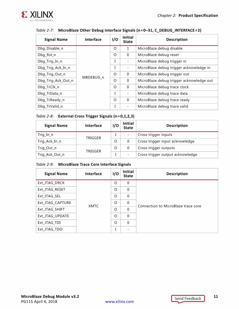
Table 2-7: MicroBlaze Other Debug Interface Signals (n = 0–31, C_DEBUG_INTERFACE≠2)
Signal Name Interface I/O InitialState Description
Dbg_Disable_n
MBDEBUG_n
O 1 MicroBlaze debug disable
Dbg_Rst_n O 0 MicroBlaze debug reset
Dbg_Trig_In_n I - MicroBlaze debug trigger in
Dbg_Trig_Ack_In_n I - MicroBlaze debug trigger acknowledge in
Dbg_Trig_Out_n O 0 MicroBlaze debug trigger out
Dbg_Trig_Ack_Out_n O 0 MicroBlaze debug trigger acknowledge out
Dbg_TrClk_n O 0 MicroBlaze debug trace clock
Dbg_TrData_n I - MicroBlaze debug trace data
Dbg_TrReady_n O 0 MicroBlaze debug trace ready
Dbg_TrValid_n I - MicroBlaze debug trace valid
Table 2-8: External Cross Trigger Signals (n = 0,1,2,3)
Signal Name Interface I/O InitialState Description
Trig_In_nTRIGGER
I - Cross trigger inputs
Trig_Ack_In_n O 0 Cross trigger input acknowledge
Trig_Out_nTRIGGER
O 0 Cross trigger outputs
Trig_Ack_Out_n I - Cross trigger output acknowledge
Table 2-9: MicroBlaze Trace Core Interface Signals
Signal Name Interface I/O InitialState Description
Ext_JTAG_DRCK
XMTC
O 0
Connection to MicroBlaze trace core
Ext_JTAG_RESET O 0
Ext_JTAG_SEL O 0
Ext_JTAG_CAPTURE O 0
Ext_JTAG_SHIFT O 0
Ext_JTAG_UPDATE O 0
Ext_JTAG_TDI O 0
Ext_JTAG_TDO I -
Send Feedback

MicroBlaze Debug Module v3.2 12PG115 April 4, 2018 www.xilinx.com
Chapter 2: Product Specification
Table 2-10: External BSCAN Interface Signals (C_USE_BSCAN = 2 or 4)
Signal Name Interface I/O InitialState Description
bscan_ext_tdi
BSCAN
I -
Connection to external BSCAN or Debug Bridge
bscan_ext_reset I -
bscan_ext_shift I -
bscan_ext_update I -
bscan_ext_capture I -
bscan_ext_sel I -
bscan_ext_drck I -
bscan_ext_tdo O 0
bscan_ext_bscanid_en(1) I -
bscan_ext_tck(1) I 0
Notes: 1. Only available when parameter C_BSCANID is not equal to 0.
Table 2-11: AXI4-Stream Trace Output (C_TRACE_OUTPUT = 2)
Signal Name Interface I/O InitialState Description
M_AXIS_TDATA[C_M_AXIS_DATA_WIDTH-1:0]
TRACE
O - Connection to external trace compatible with the Zynq Fabric Trace Monitor, FTM (see the Zynq-7000 All Programmable SoC, Technical Reference Manual (UG585) [Ref 7])
M_AXIS_TID[C_M_AXI_ID_WIDTH-1:0] O -
M_AXIS_TVALID O -
M_AXIS_TREADY I 1
Table 2-12: External Trace Output (C_TRACE_OUTPUT = 1)
Signal Name Interface I/O InitialState Description
TRACE_DATA[C_TRACE_DATA_WIDTH-1:0]
TRACE
O - Connection to external trace equivalent to the Zynq Trace Packet Output, TPIU, port (see the Zynq-7000 All Programmable SoC, Technical Reference Manual (UG585) [Ref 7])
TRACE_CTL O -
TRACE_CLK(1) I -
TRACE_CLK_OUT(2) O -
Notes: 1. The nominal frequency of TRACE_CLK is 200 MHz. If another clock frequency is used, the parameter
C_TRACE_CLK_FREQ_HZ is set from the connected input clock (by propagation in Vivado IP Integrator) if possible, but must otherwise be manually changed accordingly.
2. The frequency of TRACE_CLK_OUT is TRACE_CLK divided by 2, nominally 100 MHz with a 90° phase shift, to create a sample point at a stable point of the outputs. The phase shift can be adjusted manually with the parameter C_TRACE_CLK_OUT_PHASE if necessary.
Send Feedback

MicroBlaze Debug Module v3.2 13PG115 April 4, 2018 www.xilinx.com
Chapter 2: Product Specification
Register SpaceIn the following tables Access is indicated by R for read-only, W for write-only and R/W for Read/Write.
AXI Slave Register SpaceTable 2-13 describes the MDM core registers accessible through the AXI4-Lite slave interface.
Table 2-13: MDM Core AXI4-Lite Slave Registers
Register Name Size (bits) Address Offset Access Description
JTAG UART Registers (C_USE_UART = 1)UART_RX_FIFO 8 0x00 R JTAG UART receive data
UART_TX_FIFO 8 0x04 W JTAG UART transmit data
UART_STATUS 8 0x08 R JTAG UART status
UART_CTRL 8 0x0C W JTAG UART control
Debug Register Access (C_DBG_REG_ACCESS = 1)
DBG_STATUS 1 0x10 R Debug register access statusbit 0 - Access lock acquired
DBG_CTRL 20 0x10 W Debug register access control
DBG_DATA 32 0x14 R/W Debug register access dataRead data or Write data
DBG_LOCK 16 0x18 W Debug register access lock
Parallel Debug Register Access (C_DBG_REG_ACCESS = 1, C_DEBUG_INTERFACE > 0)PCCTRLR 8 0x5440 W MicroBlaze Performance Counter Control
PCCMDR 5 0x5480 W MicroBlaze Performance Counter Command
PCSR 2 0x54C0 R MicroBlaze Performance Counter Status
PCDRR 32 0x5580 R MicroBlaze Performance Counter Data Read
PCDWR 32 0x55C0 W MicroBlaze Performance Counter Data Write
TCTRLR 22 0x5840 W MicroBlaze Trace Control
TCMDR 4 0x5880 W MicroBlaze Trace Command
TSR 18 0x58C0 R MicroBlaze Trace Status
TDRR 18 0x5980 R MicroBlaze Trace Data Read
PCTRLR 8 0x5C40 W MicroBlaze Profiling Control
PLAR 30 0x5C80 W MicroBlaze Profiling Low Address
PHAR 30 0x5CC0 W MicroBlaze Profiling High Address
PBAR 9-14 0x5D00 W MicroBlaze Profiling Buffer Address
PDRR 36 0x5D80-0x5D84 R MicroBlaze Profiling Data Read
PDWR 32 0x5DC0 W MicroBlaze Profiling Data Write
Send Feedback

MicroBlaze Debug Module v3.2 14PG115 April 4, 2018 www.xilinx.com
Chapter 2: Product Specification
The JTAG UART registers are identical to the AXI UART Lite registers (see the AXI UART Lite LogiCORE IP Product Guide (PG142) [Ref 4]), except that the Status register bits 5–7 (Overrun Error, Frame Error, Parity Error) are never set, and the Control register bit 2 is not reserved.
The Parallel Debug Access registers are MicroBlaze registers directly accessed through parallel debug interface (see the MicroBlaze Processor Reference Guide (UG984) [Ref 5]). The MicroBlaze processors selected when accessing these registers are determined by the Which MicroBlaze Debug register.
The MDM core always responds to accesses within the defined address space. When Parallel Debug Register Access is enabled, the address space is 0x0000–0x7FFF; when Debug Register Access is enabled it is 0x00–0x1F; when JTAG UART is enabled it is 0x0–0xF. For any unused addresses, or when the Debug Register Access is locked, write requests are ignored and read requests return zero data.
UART Receive FIFO Register (UART_RX_FIFO)This 16-entry-deep FIFO contains data received by the UART from JTAG. The FIFO bit definitions are shown in Table 2-15. Reading this register results in reading the data word from the top of the FIFO. When a read request is issued to an empty FIFO, a bus error (SLVERR) is generated and the result is undefined. The register is a read-only register. Issuing a write request to the receive data FIFO does nothing but generates a successful write acknowledgment. Table 2-14 shows the location for data on the AXI slave interface. The register is only implemented if C_USE_UART is set to 1.
UART Transmit FIFO Register (UART_TX_FIFO)This 16-entry-deep FIFO contains data to be output by the UART using JTAG. The FIFO bit definitions are shown in Table 2-17. Data to be transmitted is written into this register. When a write request is issued while the FIFO is full, a bus error (SLVERR) is generated and the data is not written into the FIFO. This is a write-only location. Issuing a read request to the transmit data FIFO generates the read acknowledgment with zero data. Table 2-16 shows the location for data on the AXI interface. The register is only implemented if C_USE_UART is set to 1.
Table 2-14: UART Receive FIFO Register (UART_RX_FIFO)Reserved UART_RX
31 8 7 0
Table 2-15: UART Receive FIFO Register Bit Definitions
Bits Name Access Reset Value Description31:8 - R 0 Reserved
7:0 UART_RX R 0 UART Receive Data
Table 2-16: UART Transmit FIFO Register (UART_TX_FIFO)Reserved UART_TX
31 8 7 0
Send Feedback

MicroBlaze Debug Module v3.2 15PG115 April 4, 2018 www.xilinx.com
Chapter 2: Product Specification
UART Status Register (UART_STATUS)
The status register contains the status of the receive and transmit data FIFOs, and when interrupt is enabled. This is a read only register. If a write request is issued to the status register it will do nothing but generate write acknowledgment. Bit assignment in the register is shown in Table 2-18 and described in Table 2-19. The register is only implemented if C_USE_UART is set to 1.
Table 2-17: UART Transmit FIFO Register Bit Definitions
Bits Name Access Reset Value Description31:8 - R 0 Reserved
7:0 UART_TX R 0 UART Transmit Data
Table 2-18: UART Status Register (UART_STATUS)Reserved UART_STATUS
31 5 4 0
Table 2-19: UART Status Register Bit Definitions
Bits Name Access Reset Value Description
31-5 Reserved N/A 0 Reserved
4 Interrupt Enabled R 0Indicates that interrupt is enabled.
0 = Interrupt is disabled1 = Interrupt is enabled
3 TX FIFO Full R 0Indicates if the transmit FIFO is full.
0 = Transmit FIFO is not full1 = Transmit FIFO is full
2 TX FIFO Empty R 1Indicates if the transmit FIFO is empty.
0 = Transmit FIFO is not empty1 = Transmit FIFO is empty
1 RX FIFO Full R 0Indicates if the receive FIFO is full.
0 = Receive FIFO is not full1 = Receive FIFO is full
0 RX FIFO Valid Data R 0Indicates if the receive FIFO has valid data.
0 = Receive FIFO is empty1 = Receive FIFO has valid data
Send Feedback
MicroBlaze Debug Module v3.2 16PG115 April 4, 2018 www.xilinx.com
Chapter 2: Product Specification
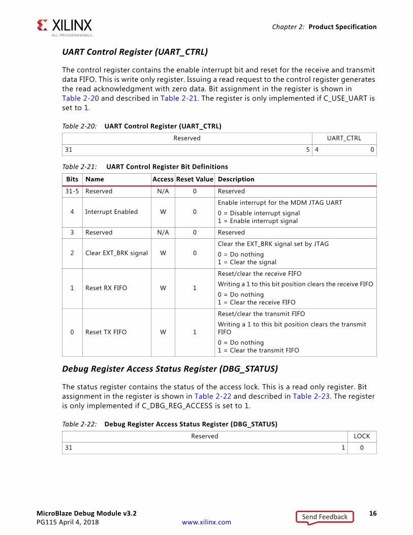
UART Control Register (UART_CTRL)
The control register contains the enable interrupt bit and reset for the receive and transmit data FIFO. This is write only register. Issuing a read request to the control register generates the read acknowledgment with zero data. Bit assignment in the register is shown in Table 2-20 and described in Table 2-21. The register is only implemented if C_USE_UART is set to 1.
Debug Register Access Status Register (DBG_STATUS)
The status register contains the status of the access lock. This is a read only register. Bit assignment in the register is shown in Table 2-22 and described in Table 2-23. The register is only implemented if C_DBG_REG_ACCESS is set to 1.
Table 2-20: UART Control Register (UART_CTRL)Reserved UART_CTRL
31 5 4 0
Table 2-21: UART Control Register Bit Definitions
Bits Name Access Reset Value Description
31-5 Reserved N/A 0 Reserved
4 Interrupt Enabled W 0Enable interrupt for the MDM JTAG UART
0 = Disable interrupt signal1 = Enable interrupt signal
3 Reserved N/A 0 Reserved
2 Clear EXT_BRK signal W 0Clear the EXT_BRK signal set by JTAG
0 = Do nothing1 = Clear the signal
1 Reset RX FIFO W 1
Reset/clear the receive FIFO
Writing a 1 to this bit position clears the receive FIFO
0 = Do nothing1 = Clear the receive FIFO
0 Reset TX FIFO W 1
Reset/clear the transmit FIFO
Writing a 1 to this bit position clears the transmit FIFO
0 = Do nothing1 = Clear the transmit FIFO
Table 2-22: Debug Register Access Status Register (DBG_STATUS)Reserved LOCK
31 1 0
Send Feedback

MicroBlaze Debug Module v3.2 17PG115 April 4, 2018 www.xilinx.com
Chapter 2: Product Specification
Debug Register Access Control Register (DBG_CTRL)
The control register is used to set up the debug register access by selecting the register bit size, register address (MDM command), whether an MDM or MicroBlaze register is accessed, and access locking. This is a write-only register. Issuing a read request to the control register generates the read acknowledgment with zero data. Writing to the register has no effect until unlocked using the DBG_LOCK register. Bit assignment in the register is shown in Table 2-24 and described in Table 2-25. The register is only implemented if C_DBG_REG_ACCESS is set to 1.
Debug Register Access Data Register (DBG_DATA)
The data register is used to read data from or write data to the debug register indicated by the DBG_CTRL register. Accessing the register has no effect until unlocked using the DBG_LOCK register. Bit assignment in the register is shown in Table 2-26. The register is only implemented if C_DBG_REG_ACCESS is set to 1.
Table 2-23: Debug Register Access Status Register Bit Definitions
Bits Name Access ResetValue Description
31-1 Reserved N/A 0 Reserved
0 Access Lock R 0Indicates the access lock status.
0 = The lock is not acquired1 = The lock has been acquired by the JTAG interface
Table 2-24: Debug Register Access Control Register (DBG_CTRL)Reserved DBG_CTRL
31 20 19 0
Table 2-25: Debug Register Access Control Register Bit Definitions
Bits Name Access ResetValue Description
31-20 Reserved N/A 0 Reserved
19-18 Access Lock Type W 00
Access lock type write:
00 = Release access lock to abort atomic sequence01 = Lock before first data access and unlock after last10 = Lock before first data access, otherwise keep lock11 = Force lock acquisition, even if acquired by JTAG
17 Access MDM W 0Access MDM or MicroBlaze Debug register:0 = MicroBlaze debug register access1 = MDM debug register access
16-9 MDM Command W 0 MDM command, see Table 2-28
8-0 Bit Size W 0 Number of bits in the accessed debug register - 1
Send Feedback

MicroBlaze Debug Module v3.2 18PG115 April 4, 2018 www.xilinx.com
Chapter 2: Product Specification
Debug Register Access Locking Register (DBG_LOCK)
The lock register is used to unlock access to the AXI Debug register access registers DBG_CTRL and DBG_DATA by writing the magic value 0xebab. Writing any other value locks access. This is a write only register. Bit assignment in the register is shown in Table 2-27. The register is only implemented if C_DBG_REG_ACCESS is set to 1.
For details on how to use the Debug Register Access, see Debug Register Access Sequence.
MDM Core InterruptsIf the interrupt enable register bit in the JTAG UART control register is set, the UART raises the interrupt signal in the cycle when the TX FIFO goes empty, or in every cycle where the RX FIFO has data available.
Debug Register SpaceThe user-accessible MDM core Debug registers are listed and described in Table 2-28. These registers are accessible using the Debug register access functionality. The values to write to the DBG_CTRL MDM register when accessing the MDM core Debug registers are also listed in the table.
Additional MDM core commands are used to access MicroBlaze extended debug features, as defined in the MicroBlaze Processor Reference Guide (UG984) [Ref 5].
All other MDM core commands are reserved for Xilinx internal use, to handle the JTAG debug protocol, including the JTAG UART and AXI Memory Access From Debug.
Table 2-26: Debug Register Access Data Register (DBG_DATA)DBG_DATA
31 0
Table 2-27: Debug Register Access Locking Register (DBG_LOCK)Reserved DBG_LOCK
31 16 15 0
Table 2-28: MDM Core User-Accessible Debug Registers
Register Name Size(bits)
MDMCommand
DBG_CTRLValue Access Description
GeneralMDMConfiguration 32 00001100 0x6181F R The MDM configuration.
MDM ExtendedConfiguration 35 00001100 0x61822 R The MDM extended configuration.
Send Feedback

MicroBlaze Debug Module v3.2 19PG115 April 4, 2018 www.xilinx.com
Chapter 2: Product Specification
Which MicroBlaze(1) 8-32 00001101
8: 0x61A079: 0x61A08
...32: 0x61A1F
W Which MicroBlaze processors to access. This register has a variable bit size.
Cross Trigger Debug Registers (C_USE_CROSS_TRIGGER = 1)
External CrossTrigger Control 10 01000000 0x68009 W
External cross trigger control register, used to set the trigger output source, and trigger input mask for each of the four triggers.
Cross TriggerControl 16 01000110 0x68C0F W
Cross trigger control register, used to set the trigger output source, trigger input mask and logic function to combine inputs for each of the eight triggers.
Cross TriggerStatus 24 01000010 0x68417 R
Cross trigger status register to read the current values of all trigger inputs and outputs.
External Trace Register (C_TRACE_OUTPUT = 1)
External TraceControl 14 01001110 0x69C0D W
External trace control register, used to control test pattern generation and trigger output.
AXI4-Stream Trace Register (C_TRACE_OUTPUT = 2)AXI4-Stream TraceControl 8 01001110 0x69C07 W AXI4-Stream trace control register, used
to set delay between output packets.
AXI4-Master Trace Registers (C_TRACE_OUTPUT = 3)
AXI4-Master TraceStatus 3 01001010 0x69402 R
AXI4-Master trace status register, with buffer wrap and bus interface response status.
AXI4-Master TraceCurrent Address 32 01001011 0x6961F R AXI4-Master trace current address
register, with the current buffer address.
AXI4-Master TraceLow Address 16 01001100 0x6980F W AXI4-Master trace low address register,
used to define the buffer low address.
AXI4-Master TraceHigh Address 16 01001101 0x69A0F W AXI4-Master trace high address register,
used to define the buffer high address.
AXI4-Master TraceControl 1 01001110 0x69C00 W AXI4-Master trace control register, used
to define buffer full behavior.
Notes: 1. 8 to 32 bits, depending on the number of connected MicroBlaze cores. For fewer than eight cores, the register is 8
bits.
Table 2-28: MDM Core User-Accessible Debug Registers (Cont’d)
Register Name Size(bits)
MDMCommand
DBG_CTRLValue Access Description
Send Feedback

MicroBlaze Debug Module v3.2 20PG115 April 4, 2018 www.xilinx.com
Chapter 2: Product Specification
MDM Configuration Debug Register
This register contains the current MDM core configuration. This register is a read-only register. Issuing a write request to the register does nothing.
MDM Extended Configuration Debug Register
This register contains the current extended MDM core configuration. This register is a read-only register. Issuing a write request to the register does nothing. The register is only available if the MDM Configuration Debug register bit 22 is set.
Table 2-29: MDM Configuration Debug RegisterMagic Res Ext UART Width Ports Version
31 24 23 22 21 20 16 15 8 7 0
Table 2-30: MDM Configuration Debug Register Bit Definitions
Bits Name Access Value Description31 - 24 Magic R 0x42 Magic value 0x42
23 Reserved R 1 Reserved
22 Extended R 0, 1 Set to 1 if extended configuration register is available
21 UART R 0, 1 Parameter C_USE_UART
20 - 16 Width R 00111 JTAG UART character width - 1, 8 bit characters
15 - 8 Ports R 1-32 Parameter C_MB_DBG_PORTS
7 - 0 Version R 0x67 Version of MDM and JTAG UART protocol
Table 2-31: MDM Extended Configuration Debug RegisterTO CT RA MA Magic Res Ext UART Width Ports Version
36-35 34 33 32 31 24 23 22 21 20 16 15 8 7 0
Table 2-32: MDM Extended Configuration Debug Register Bit Definitions
Bits Name Access Value Description36 - 35 Trace Output R 0,1,2,3 Parameter C_TRACE_OUTPUT
34 Cross Trigger R 0, 1 Parameter C_USE_CROSS_TRIGGER
33 Register Access R 0, 1 Parameter C_DBG_REG_ACCESS
32 Memory Access R 0, 1 Parameter C_DBG_MEM_ACCESS
31 - 0 N/A R N/A See Table 2-30
Send Feedback

MicroBlaze Debug Module v3.2 21PG115 April 4, 2018 www.xilinx.com
Chapter 2: Product Specification
Which MicroBlaze Debug Register
This register defines which MicroBlaze processor or processors are accessed. This register is a write-only register. Issuing a read request has no effect, and undefined data is read.
It is possible to write to the debug registers of more than one processor simultaneously, by setting more than one bit in this register. When reading from a debug register, only one bit must be set in this register, otherwise read data is undefined.
The register bit size is variable, and depends on the C_MB_DBG_PORTS parameter:
• When C_MB_DBG_PORTS set to 1, the register is not used, and the only connected processor is always accessed.
• When C_MB_DBG_PORTS ranges from 2 to 8, the register has 8 bits.
• When C_MB_DBG_PORTS is greater than 8, the register has the same number of bits as the parameter.
The processors are defined from the right in the register according to Table 2-34.
Table 2-33: Which MicroBlaze Debug Register
31 8 7 0
Table 2-34: Which MicroBlaze Debug Register Bit Definitions
C_MB_DBG_PORTS Bits Access Reset Value Description
2 1 - 0 W 0 Bit 0 = Access processor number 0Bit 1 = Access processor number 1
3 2 - 0 W 0Bit 0 = Access processor number 0Bit 1 = Access processor number 1Bit 2 = Access processor number 2
... ... ... ... ...
8 7 - 0 W 0Bit 0 = Access processor number 0...Bit 7 = Access processor number 7
8 - 32 (n-1) - 0 W 0Bit 0 = Access processor number 0...Bit n-1 = Access processor number n-1
Send Feedback

MicroBlaze Debug Module v3.2 22PG115 April 4, 2018 www.xilinx.com
Chapter 2: Product Specification
External Cross Trigger Control Debug Register
This register defines the trigger source for each of the four external trigger outputs, and the mask for each of the four external trigger inputs. This register is a write-only register. It is only available when the C_USE_CROSS_TRIGGER parameter is set. Issuing a read request has no effect, and undefined data is read.
The reset values of Input Mask and Output Select for each trigger are defined by the parameter C_EXT_TRIG_RESET_VALUE:
• Bits 19-16: Input Mask
• Bits 15-12: External Trigger 0 Output Select
• Bits 11-8: External Trigger 1 Output Select
• Bits 7-4: External Trigger 2 Output Select
• Bits 3-0: External Trigger 3 Output Select
Cross Trigger Control Debug Register
This register defines trigger source for each of the eight trigger outputs, and the mask for each of the eight trigger inputs. This register is a write-only register. Issuing a read request has no effect, and undefined data is read.
Table 2-35: External Cross Trigger Control Debug RegisterReserved External Trigger
31 10 9 0
Table 2-36: External Cross Trigger Control Debug Register Bit Definitions
Bits Name Access Reset Value Description31 - 10 Reserved N/A 0 Reserved
9 - 6 Output Select W See Notes(1) Trigger output source for the selected external trigger output, according to Table 2-39.
5 - 2 Input Mask W See Notes(1)
Mask bits for each external trigger input for the selected trigger output. Bits with value 0 do not affect the output.
Bit 5 = External trigger input 0...Bit 2 = External trigger input 3
1 - 0 Index W 00
Selected external trigger output to change:
00 = External Trigger 001 = External Trigger 110 = External Trigger 211 = External Trigger 3
Notes: 1. The default reset value is defined by the parameter C_EXT_TRIG_RESET_VALUE to set Input Mask to 1111 and Output
Select to 1 for External Trigger 0, 2 for External Trigger 1, 3 for External Trigger 2 and 4 for External Trigger 3.
Send Feedback

MicroBlaze Debug Module v3.2 23PG115 April 4, 2018 www.xilinx.com
Chapter 2: Product Specification
Writing the register affects the cross trigger outputs of the MicroBlaze processor or processors selected by the Which MicroBlaze Debug register.
See the MicroBlaze Processor Reference Guide (UG984) [Ref 5], for the definition of the eight MicroBlaze trigger inputs and outputs.
Table 2-37: Cross Trigger Control Debug RegisterReserved Trigger
31 16 15 0
Table 2-38: Cross Trigger Control Debug Register Bit Definitions
Bits Name Access Reset Value Description31 - 16 Reserved N/A 0 Reserved
15 - 12 Output Select W See Notes(1) Trigger output source for the selected MicroBlaze trigger output, according to Table 2-39.
11 - 4 Input Mask W 11111111
Mask bits for each MicroBlaze trigger input for the selected trigger output. Bits with value 0 do not affect the output.
Bit 11 = MicroBlaze Trigger input 0...Bit 4 = MicroBlaze Trigger input 7
3 And/Or W 0Logic function to combine inputs:
0 = Logic or, triggers if any input is set1 = Logic and, triggers only if all inputs are set
2 - 0 Index W 000
Selected MicroBlaze trigger output to change:
000 = MicroBlaze Trigger output 0...111 = MicroBlaze Trigger output 7
Notes: 1. The reset value is 9 for Trigger 0, 10 for Trigger 1, 11 for Trigger 2, 12 for Trigger 3, and 13 for Trigger 4-7.
Table 2-39: Cross Trigger Output Select Field Definition
Field Value Name Description0000 Static One Static one, no input selected
0001 - 1000 Trigger Input0001 = Select MicroBlaze Trigger Input 0...1000 = Select MicroBlaze Trigger Input 7
1001 - 1100 External Trigger Input1001 = Select External Trigger Input 0...1100 = Select External Trigger Input 3
1101 Static Zero Static zero, no input selected
1110 - 1111 Reserved Reserved
Send Feedback

MicroBlaze Debug Module v3.2 24PG115 April 4, 2018 www.xilinx.com
Chapter 2: Product Specification
Cross Trigger Status Debug Register
This register contains the current trigger input and output values. This register is a read-only register. Issuing a write request to the register does nothing.
The MicroBlaze cross trigger status (bits 0 to 15) represents the MicroBlaze processor selected by the Which MicroBlaze Debug register. If more than one processor is selected, the result is undefined.
External Trace Control Debug Register
This register defines and starts continuous or timed test pattern generation, as well as defines direct or delayed trigger outputs on trace start and/or stop events. This register is a write-only register. Issuing a read request has no effect, and undefined data is read.
A trigger is encoded by setting TRACE_CTL = 1 and TRACE_DATA[1:0] = 10.
Table 2-40: Cross Trigger Status Debug RegisterReserved Trigger Status
31 24 23 0
Table 2-41: Cross Trigger Status Debug Register Bit Definitions
Bits Name Access Description31 - 24 Reserved N/A Reserved
23 - 16 Trigger Outputs R
Current selected MicroBlaze processor trigger output values.Bit 23 = Trigger 0...Bit 16 = Trigger 7
15 - 8 Trigger Inputs R
Current selected MicroBlaze processor trigger input values.Bit 15 = Trigger 0...Bit 8 = Trigger 7
7 - 4 External Trigger Outputs R
Current external trigger input values.Bit 7 = External Trigger Output 0...Bit 4 = External Trigger Output 3
3 - 0 External Trigger Inputs R
Current external trigger input values.Bit 3 = External Trigger Input 0...Bit 0 = External Trigger Input 3
Table 2-42: External Trace Control Debug RegisterReserved Test Pattern
SelectTrigger Enable
TPT TPC Test Pattern RepeatTrigger Delay
31 14 13 10 9 8 7 0
Send Feedback

MicroBlaze Debug Module v3.2 25PG115 April 4, 2018 www.xilinx.com
Chapter 2: Product Specification
AXI4-Stream Trace Control Debug Register
This register defines a delay in M_AXIS_ACLK clock cycles after each output packet. This register is a write-only register. Issuing a read request has no effect, and undefined data is read.
This delay is primarily intended to avoid downstream FIFO overflow, which can occur for AXI4-Stream connections that do not implement a ready signal, such as the Zynq Fabric Trace Monitor interface (see the Zynq-7000 All Programmable SoC, Technical Reference Manual (UG585) [Ref 7]).
Table 2-43: External Trace Control Debug Register Bit Definitions
Bits Name Access ResetValue Description
31 - 14 Reserved N/A 0 Reserved
13 W1, STO W 0
Generate walking-ones test pattern, either for a duration defined by TPR when the TPT bit is set, or continuously when the TPC bit is set.
Output a trigger when trace is stopped in any processor.
12 W0, DSTO W 0
Generate walking-zeros test pattern, either for a duration defined by TPR when the TPT bit is set, or continuously when the TPC bit is set.
Output a trigger when trace is stopped after the delay defined by TD in any processor.
11 A5, STA W 0
Generate AA/55 test pattern, either for a duration defined by TPR when the TPT bit is set, or continuously when the TPC bit is set.
Output a trigger when trace is started in any processor.
10 F0, DSTA W 0
Generate FF/00 test pattern, either for a duration defined by TPR when the TPT bit is set, or continuously when the TPC bit is set.
Output a trigger when trace is started after the delay defined by TD in any processor.
9 TPT W 0Generate timed test patterns for the duration defined by TPR, for the defined patterns W1, W0, A5, and F0 in sequence. One or more of the W1, W0, A5, and F0 bits must be set.
8 TPC W 0 Generate a continuous test pattern, either the pattern W1, W0, A5, or F0. Only one of the W1, W0, A5, and F0 bits must be set.
7 - 0 TPR, TD W 0x00
Defines a test pattern duration for timed test patterns in TRACE_CLK clock cycles, 0 - 255.
Defines trigger delay for DSTOP and DSTA triggers in 256 TRACE_CLK clock cycle intervals, 0, 256, 512, …, 65280.
Table 2-44: AXI4-Stream Trace Control Debug RegisterReserved Packet Delay
31 8 7 0
Send Feedback

MicroBlaze Debug Module v3.2 26PG115 April 4, 2018 www.xilinx.com
Chapter 2: Product Specification
AXI4-Master Trace Status Debug Register
This register defines whether trace has wrapped when the external memory buffer is full, and whether an AXI4-Master write has failed with a non-zero response. This register is a read-only register. Issuing a write request has no effect.
The status is cleared by writing to the AXI4-Master Trace Control Debug register.
AXI4-Master Trace Current Address Debug Register
This register defines the first free location in the AXI4-Master external memory buffer. The register is incremented by 0x50 (20 32-bit words) for every trace packet written to the external memory buffer. This register is a read-only register. Issuing a write request has no effect.
If the FS bit is cleared in the AXI4-Master Trace Control Debug register, the current address will wrap around to the low address, defined by the AXI4-Master Trace Buffer Low Address, when it would have incremented past the high address, defined by the AXI4-Master Trace Buffer High Address.
The current address is reset to the low address, defined by the AXI4-Master Trace Buffer Low Address, by writing to the AXI4-Master Trace Control Debug register.
Table 2-45: AXI4-Stream Trace Control Debug Register Bit Definitions
Bits Name Access Reset Value Description31 - 8 Reserved N/A 0 Reserved
7 - 0 Packet Delay W 0x00 Delay in M_AXIS_ACLK clock cycles between each word in the output packet, 0 - 255.
Table 2-46: AXI4-Master Trace Status Debug RegisterReserved Wrap Response
31 3 2 1 0
Table 2-47: AXI4-Master Trace Status Debug Register Bit Definitions
Bits Name Access ResetValue Description
31 - 3 Reserved N/A 0 Reserved
2 Wrap R 0 This bit indicates if the current address has wrapped around.
1 - 0 Response R 00The AXI4-Master write response, M_AXI_BRESP. The response is sticky - as soon as a non-zero response has occurred, the bits remain set.
Table 2-48: AXI4-Master Trace Current Address Debug RegisterCurrent Address
31 0
Send Feedback

MicroBlaze Debug Module v3.2 27PG115 April 4, 2018 www.xilinx.com
Chapter 2: Product Specification
AXI4-Master Trace Buffer Low Address Debug Register
This register defines the AXI4-Master low address of the external trace memory buffer, with a 64KB granularity. This register is a write-only register. Issuing a read request has no effect, and undefined data is read.
AXI4-Master Trace Buffer High Address Debug Register
This register defines the AXI4-Master high address of the external trace memory buffer, with a 64KB granularity. This register is a write-only register. Issuing a read request has no effect, and undefined data is read.
AXI4-Master Trace Control Debug Register
This register defines whether trace is stopped when the external memory buffer is full. This register is a write-only register. Issuing a read request has no effect, and undefined data is read.
Table 2-49: AXI4-Stream Trace Control Debug Register Bit Definitions
Bits Name Access Reset Value Description
31 - 0 Current Address R 0x00000000
AXI4-Master current address of memory trace buffer. This is the full 32-bit address of the first free location in the buffer.
Table 2-50: AXI4-Master Trace Buffer Low Address Debug RegisterReserved Low Address
31 16 15 0
Table 2-51: AXI4-Master Trace Buffer Low Address Debug Register Bit Definitions
Bits Name Access ResetValue Description
31 - 16 Reserved N/A 0 Reserved
15 - 0 Low Address W 0x0000 AXI4-Master low address of memory trace buffer. This is the 16
most significant bits of the 32-bit address.
Table 2-52: AXI4-Master Trace Buffer High Address Debug RegisterReserved High Address
31 16 15 0
Table 2-53: AXI4-Master Trace Buffer High Address Debug Register Bit Definitions
Bits Name Access Reset Value Description31 - 16 Reserved N/A 0 Reserved
15 - 0 High Address W 0x0000 AXI4-Master high address of memory trace buffer. This is the 16 most significant bits of the 32-bit address.
Send Feedback
MicroBlaze Debug Module v3.2 28PG115 April 4, 2018 www.xilinx.com
Chapter 2: Product Specification
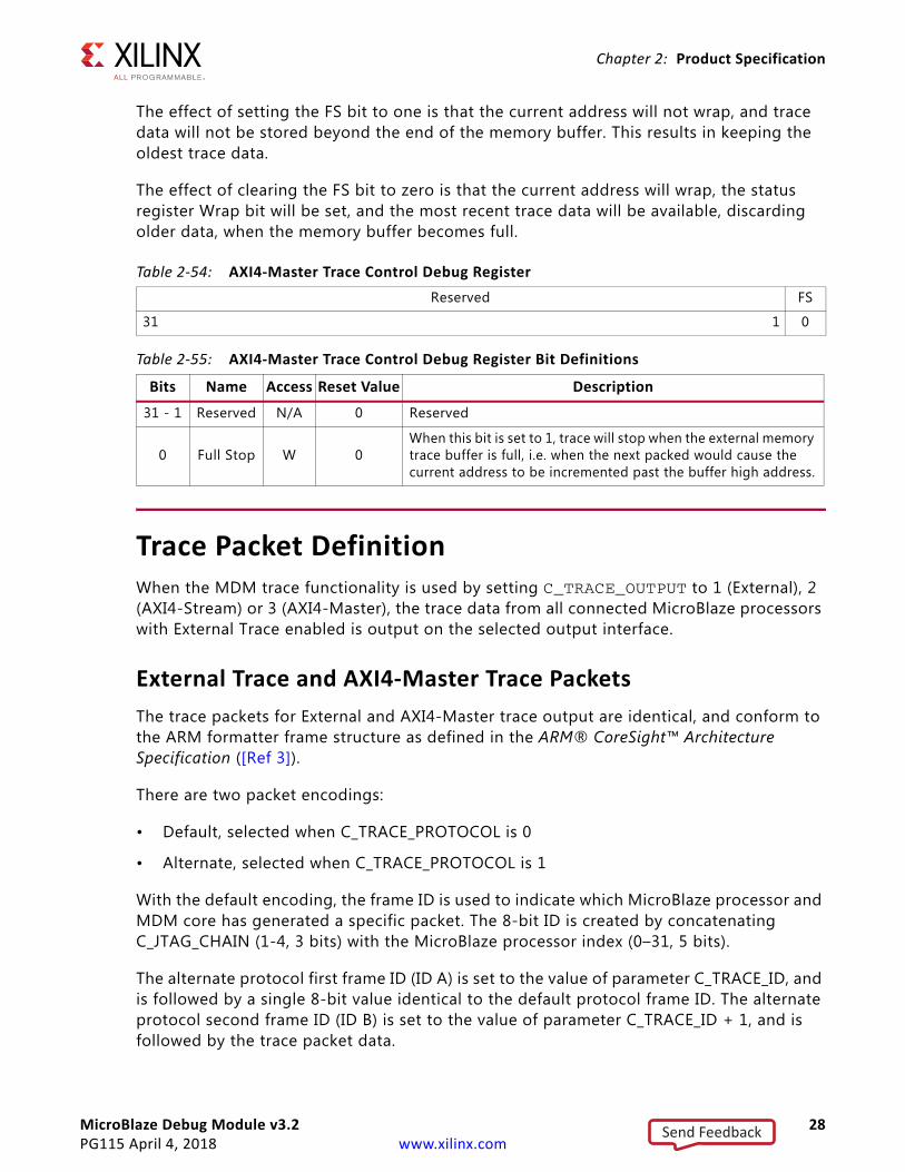
The effect of setting the FS bit to one is that the current address will not wrap, and trace data will not be stored beyond the end of the memory buffer. This results in keeping the oldest trace data.
The effect of clearing the FS bit to zero is that the current address will wrap, the status register Wrap bit will be set, and the most recent trace data will be available, discarding older data, when the memory buffer becomes full.
Trace Packet DefinitionWhen the MDM trace functionality is used by setting C_TRACE_OUTPUT to 1 (External), 2 (AXI4-Stream) or 3 (AXI4-Master), the trace data from all connected MicroBlaze processors with External Trace enabled is output on the selected output interface.
External Trace and AXI4-Master Trace PacketsThe trace packets for External and AXI4-Master trace output are identical, and conform to the ARM formatter frame structure as defined in the ARM® CoreSight™ Architecture Specification ([Ref 3]).
There are two packet encodings:
• Default, selected when C_TRACE_PROTOCOL is 0
• Alternate, selected when C_TRACE_PROTOCOL is 1
With the default encoding, the frame ID is used to indicate which MicroBlaze processor and MDM core has generated a specific packet. The 8-bit ID is created by concatenating C_JTAG_CHAIN (1-4, 3 bits) with the MicroBlaze processor index (0–31, 5 bits).
The alternate protocol first frame ID (ID A) is set to the value of parameter C_TRACE_ID, and is followed by a single 8-bit value identical to the default protocol frame ID. The alternate protocol second frame ID (ID B) is set to the value of parameter C_TRACE_ID + 1, and is followed by the trace packet data.
Table 2-54: AXI4-Master Trace Control Debug RegisterReserved FS
31 1 0
Table 2-55: AXI4-Master Trace Control Debug Register Bit Definitions
Bits Name Access Reset Value Description31 - 1 Reserved N/A 0 Reserved
0 Full Stop W 0When this bit is set to 1, trace will stop when the external memory trace buffer is full, i.e. when the next packed would cause the current address to be incremented past the buffer high address.
Send Feedback

MicroBlaze Debug Module v3.2 29PG115 April 4, 2018 www.xilinx.com
Chapter 2: Product Specification
Each packet transmits 32 18-bit trace items, and consists of 20 32-bit words, or five frames. The default packet encoding, when C_TRACE_PROTOCOL is 0 is illustrated in Table 2-56 and Figure 2-1. The alternate packet encoding, when C_TRACE_PROTOCOL is 1, is shown in Table 2-57 and Figure 2-2.
Table 2-56: External Trace and AXI4-Master Default Trace Packet Encoding
TraceItem Packet Word (w) and Bits Trace
Item Packet Word (w) and Bits
0 w2[9:8], w0[23:17], w3[25], w0[15:8] 16 w12[9:8], w10[15:1], w11[28]
1 w2[11:10], w1[7:1], w3[26], w0[31:24] 17 w12[11:10], w10[31:17], w11[29]
2 w2[13:12], w1[23:17], w3[27], w1[15:8] 18 w12[13:12], w11[15:1], w11[30]
3 w2[15:14], w2[7:1], w3[28], w1[31:24] 19 w12[15:14], w12[7:1], w15[24], w11[23:17], w11[31]
4 w4[25:24], w2[31:17], w3[29] 20 w14[17], w15[29], w12[31:17], w15[25]
5 w4[27:26], w3[15:1], w3[30] 21 w14[19:18], w13[15:1],w15[26]
6 w4[29:28], w4[7:1], w7[24], w3[23:17], w3[31] 22 w14[21:20], w13[31:17], w15[27]
7 w4[31:30], w4[23:17], w7[25], w4[15:8] 23 w14[23:22], w14[15:1], w15[28]
8 w7[1], w7[30], w5[15:1], w7[26] 24 w17[9:8], w15[7:1], w15[30], w14[31:24]
9 w7[3:2], w5[31:17], w7[27] 25 w17[11:10], w15[23:17], w15[31], w15[15:8]
10 w7[5:4], w6[15:1], w7[28] 26 w17[13:12], w16[23:17], w19[25], w16[15:8]
11 w7[7:6], w6[31:17], w7[29] 27 w17[15:14], w17[7:1], w19[26], w16[31:24]
12 w9[25:24], w7[23:17], w7[31], w7[15:8] 28 w19[17], w19[31], w17[31:17], w19[27]
13 w9[27:26], w8[23:17], w11[25], w8[15:8] 29 w19[19:18], w18[15:1], w19[28]
14 w9[29:28], w9[7:1], w11[26], w8[31:24] 30 w19[21:20], w18[31:17], w19[29]
15 w9[31:30], w9[23:17], w11[27], w9[15:8] 31 w19[23:22], w19[15:1], w19[30]
Send Feedback

MicroBlaze Debug Module v3.2 30PG115 April 4, 2018 www.xilinx.com
Chapter 2: Product Specification
X-Ref Target - Figure 2-1
Figure 2-1: External Trace and AXI4-Master Default Trace Packet Structure
Item 1 Item 0 0B Item 0 ID 1A
Item 3 Item 2 0D Item 2 Item 1 0C
Item 4 Item 4 0G Item 3-0 Item 3 0E
A Item 6 0J Item 5 Item 5 0H
01816 1517232431 7
w0
w1
w2
w3
Item 7-4 Item 7 0 Item 7 Item 6 0
Item 9 Item 9 0 Item 8 Item 8 0
Item 11 Item 11 0 Item 10 Item 10 0
Item 12 0 Item 12 Item 11-8 0
w4
w5
w6
w7
Item 14 Item 13 0 Item 13 ID 1
Item 15-12 Item 15 0 Item 15 Item 14 0
Item 17 Item 17 0 Item 16 Item 16 0
Item 19 0 Item 18 Item 18 0
w8
w9
w10
w11
Item 20 Item 20 0 Item 19-16 Item 19 0
Item 22 Item 22 0 Item 21 Item 21 0
Item 24 Item 23-20 0 Item 23 Item 23 0
Item 25 0 Item 25 Item 24 0
w12
w13
w14
w15
Item 27 Item 26 0 Item 26 ID 1
Item 28 Item 28 0 Item 27-24 Item 27 0
Item 30 Item 30 0 Item 29 Item 29 0
Item 31-28 0 Item 31 Item 31 0
w16
w17
w18
w19
Frame 0
Frame 1
Frame 2
Frame 3
Frame 4
BCDEGHJ
ABCDEGHJ
ABCDEGHJ
ABCDEGHJ
ABCDEGHJ
Send Feedback

MicroBlaze Debug Module v3.2 31PG115 April 4, 2018 www.xilinx.com
Chapter 2: Product Specification
Table 2-57: Alternate Trace Packet Encoding
TraceItem Packet Word (w) and Bits Trace
Item Packet Word (w) and Bits
0 w2[25:24], w1[7:1], w3[26], w0[31:24] 16 w12[17], w15[25], w11[23:17], w11[29], w10[15:8]
1 w2[27:26], w1[23:17], w3[27], w1[15:8] 17 w12[19:18], w11[7:1], w11[30], w10[31:24]
2 w2[29:28], w2[7:1], w3[28], w1[31:24] 18 w12[21:20], w11[23:17], w11[31], w11[15:8]
3 w2[31:30], w2[23:17], w3[29], w2[15:8] 19 w12[23:22], w12[15:1], w15[24]
4 w5[9:8], w3[15:1], w3[30] 20 w14[25:24], w13[7:1], w15[26], w12[31:24]
5 w5[11:10], w4[7:1], w7[24], w3[23:17], w3[31] 21 w14[27:26], w13[23:17], w15[27], w13[15:8]
6 w5[13:12], w4[23:17], w7[25], w4[15:8] 22 w14[29:28], w14[7:1], w15[28], w13[31:24]
7 w5[15:14], w5[7:1], w7[26], w4[31:24] 23 w14[31:30], w15[29]. w14[15:8]
8 w7[17], w7[31], w5[31:17], w7[27] 24 w17[9:8], w15[15:1], w15[30]
9 w7[19:18], w5[15:1], w7[28] 25 w17[11:10], w16[7:1]. w19[24], w15[23:17], w15[31]
10 w7[21:20], w6[31:17], w7[29] 26 w17[13:12], w16[23:17], w19[25], w16[15:8]
11 w7[23:22], w7[15:1], w7[30] 27 w17[15:14], w17[7:1], w19[26], w16[31:24]
12 w10[1], w11[28], w8[15:1], w11[24] 28 w19[17], w19[31], w17[31:17], w19[27]
13 w10[3:2], w8[31:17], w11[25] 29 w19[19:18], w18[15:1], w19[28]
14 w10[5:4], w9[15:1], w11[26] 30 w19[21:20], w18[31:17], w19[29]
15 w10[7:6], w9[31:17], w11[27] 31 w19[23:22], w19[15:1], w19[30]
Send Feedback

MicroBlaze Debug Module v3.2 32PG115 April 4, 2018 www.xilinx.com
Chapter 2: Product Specification
AXI4-Stream Trace PacketsThe trace packets for AXI4-Stream are intended to be further processed, in particular by the Zynq TPIU (see the Zynq-7000 All Programmable SoC, Technical Reference Manual (UG585) [Ref 7]). The M_AXIS_TID signals are used to indicate which MicroBlaze processor has generated a specific packet. Each packet transmits 32 18-bit trace items, and consists of 18 32-bit words. The default packet encoding, when C_TRACE_PROTOCOL is 0, is illustrated in Table 2-58 and Figure 2-3. The AXI4-Stream also supports the alternate trace protocol, when C_TRACE_PROTOCOL is 1, as described in Table 2-57 and Figure 2-2.
X-Ref Target - Figure 2-2
Figure 2-2: Alternate Trace Packet Structure
Item 0 ID B 1B ID ID A 1A
Item 2 Item 1 0D Item 1 Item 0 0C
Item 3-0 Item 3 0G Item 3 Item 2 0E
A Item 5 0J Item 4 Item 4 0H
01816 1517232431 7
w0
w1
w2
w3
Item 7 Item 6 0 Item 6 Item 5 0
Item 8 Item 8 0 Item 7-4 Item 7 0
Item 10 Item 10 0 Item 9 Item 9 0
Item 11-8 0 Item 11 Item 11 0
w4
w5
w6
w7
Item 13 Item 13 0 Item 12 Item 12 0
Item 15 Item 15 0 Item 14 Item 14 0
Item 17 Item 16 0 Item 16 Item 15-12 0
Item 18 0 Item 18 Item 17 0
w8
w9
w10
w11
Item 20 Item 19-16 0 Item 19 Item 19 0
Item 22 Item 21 0 Item 21 Item 20 0
Item 23-20 Item 23 0 Item 23 Item 22 0
Item 25 0 Item 24 Item 24 0
w12
w13
w14
w15
Item 27 Item 26 0 Item 26 Item 25 0
Item 28 Item 28 0 Item 27-24 Item 27 0
Item 30 Item 30 0 Item 29 Item 29 0
Item 31-28 0 Item 31 Item 31 0
w16
w17
w18
w19
Frame 0
Frame 1
Frame 2
Frame 3
Frame 4
BCDEGHJ
ABCDEGHJ
ABCDEGHJ
ABCDEGHJ
ABCDEGHJ
Send Feedback

MicroBlaze Debug Module v3.2 33PG115 April 4, 2018 www.xilinx.com
Chapter 2: Product Specification
Table 2-58: AXI4-Stream Default Trace Packet Encoding
Trace Item Packet Word (w) and Bits Trace Item Packet Word (w) and Bits0 w2[1:0], w0[15:0] 16 w11[1:0], w9[15:0]
1 w2[3:2], w0[31:16] 17 w11[3:2], w9[31:16]
2 w2[5:4], w1[15:0] 18 w11[5:4], w10[15:0]
3 w2[7:6], w1[31:16] 19 w11[7:6], w10[31:16]
4 w4[9:8], w2[23:8] 20 w13[9:8], w11[23:8]
5 w4[11:10], w3[7:0], w2[31:24] 21 w13[11:10], w12[7:0], w11[31:24]
6 w4[13:12], w3[23:8] 22 w13[13:12], w12[23:8]
7 w4[15:14], w4[7:0], w3[31:24] 23 w13[15:14], w13[7:0], w12[31:24]
8 w6[17:16], w4[31:16] 24 w15[17:16], w13[31:16]
9 w6[19:18], w5[15:0] 25 w15[19:18], w14[15:0]
10 w6[21:20], w5[31:16] 26 w15[21:20], w14[31:16]
11 w6[23:22], w6[15:0] 27 w15[23:22], w15[15:0]
12 w8[25:24], w7[7:0], w6[31:24] 28 w17[25:24], w16[7:0], w15[31:24]
13 w8[27:26], w7[23:8] 29 w17[27:26], w16[23:8]
14 w8[29:28], w8[7:0], w7[31:24] 30 w17[29:28], w17[7:0], w16[31:24]
15 w8[31:30], w8[23:8] 31 w17[31:30], w17[23:8]
X-Ref Target - Figure 2-3
Figure 2-3: AXI4-Stream Default Trace Packet Structure
Item 1 Item 1 Item 0 Item 0w0
Item 3 Item 3 Item 2 Item 2w1
Item 5 Item 4 Item 4 Item 3-0w2
Item 7 Item 6 Item 6 Item 5w3
Item 8 Item 8 Item 7-4 Item 7w4
Item 10 Item 10 Item 9 Item 9w5
Item 12 Item 11-8 Item 11 Item 11w6
Item 14 Item 13 Item 13 Item 12w7
Item 15-12 Item 15 Item 15 Item 14w8
Item 17 Item 17 Item 16 Item 16w9
Item 19 Item 19 Item 18 Item 18w10
Item 21 Item 20 Item 20 Item 19-16w11
Item 23 Item 22 Item 22 Item 21w12
Item 24 Item 24 Item 23-20 Item 23w13
Item 26 Item 26 Item 25 Item 25w14
Item 28 Item 27-24 Item 27 Item 27w15
Item 30 Item 29 Item 29 Item 28w16
Item 31-28 Item 31 Item 31 Item 30w17
31 24 23 16 15 8 7 0
Send Feedback

MicroBlaze Debug Module v3.2 34PG115 April 4, 2018 www.xilinx.com
Chapter 3
Designing with the CoreThis chapter includes guidelines and additional information to facilitate designing with the core.
General Design GuidelinesThe MicroBlaze™ Debug Module supports multiple MicroBlaze cores, making it possible to use one MDM core for multiprocessor systems with up to 32 processors.
The MDM core outputs, Ext_BRK and Ext_NM_BRK, are not currently used, and need not be connected to MicroBlaze.
When using the JTAG-based UART, the MDM core Interrupt output can be connected to an interrupt controller to provide interrupt-driven serial output. If this signal is not connected, only polled-mode serial output is available.
When using the JTAG memory access, the AXI4 Master should be connected to access the system memory accessible by the connected MicroBlaze cores, usually through the processor cache interfaces M_AXI_DC and M_AXI_IC. Depending on the AXI interconnect topology, this might exclude peripheral I/O accessed through the processor peripheral interface M_AXI_DP. The LMB Master ports should be connected to access the LMB local memory of the corresponding processor. This can be done by adding an additional LMB slave input to the data-side LMB BRAM Interface Controller (see the LogiCORE IP LMB BRAM Interface Controller Product Guide (PG112) [Ref 6]).
Parallel debug can be selected to improve timing in cases where timing closure is difficult to achieve with serial debug, in particular on stacked silicon interconnect (SSI) devices where the MDM core is placed in the master super logic region (SLR), and one or more MicroBlaze cores are placed in other regions. In this case it is suitable to configure both the MDM and MicroBlaze to use AXI parallel debug, which allows clocking of the debug signals between MDM and MicroBlaze using an AXI Register Slice. See LogiCORE AXI Interconnect IP Product Guide (PG059) [Ref 12] for more information on how to use the AXI Register Slice.
When using internal BSCAN in SSI devices, the MDM placement is constrained to the master Super Logic Region (SLR1).
When using external BSCAN for debugging with the Xilinx Virtual Cable (XVC), the MDM is connected to a Debug Bridge IP core. This connection is normally automatically inferred by the Vivado Design Suite, and in this case the MDM BSCAN location should be configured to select EXTERNAL HIDDEN to hide the bus interface in Vivado IP integrator. If an explicit
Send Feedback

MicroBlaze Debug Module v3.2 35PG115 April 4, 2018 www.xilinx.com
Chapter 3: Designing with the Core
connection needs to be made, configure the BSCAN location as EXTERNAL instead. For further details on the Debug Bridge, see the Debug Bridge LogiCORE IP Product Guide (PG245) [Ref 15].
ClockingThe S_AXI_ACLK input is only used when the JTAG-based UART or Debug register access is enabled, and AXI4-Lite slave interconnect is used, or when BSCAN is disabled. Then it should normally be set to the same clock as the interconnect.
The M_AXI_ACLK input is used when JTAG Memory Access is enabled, and AXI4 master interconnect and/or LMB master interface is used. Then it must be set to the same clock as the interconnect and LMB interface. Different clocks for AXI4 and LMB is not supported in this case. The M_AXI_ACLK input is also used when AXI4 master trace output is selected. Then it must be set to the same clock as the interconnect. It can be asynchronous to other clocks. The LMB interface is not used in this case.
The M_AXIS_ACLK is used when AXI4-Stream trace output is selected. Then it should be set to the same clock as the AXI4-Stream slave the trace interface is connected to. It can be asynchronous to all other clocks.
The TRACE_CLK input clock is used when external trace output is selected. This clock could be generated on-chip or be derived from an off-chip source. It can be asynchronous to all other clocks. The nominal clock frequency is 200 MHz. If another clock frequency is used, the parameter C_TRACE_CLK_FREQ_HZ must be manually changed accordingly.
The TRACE_CLK_OUT output clock is a divided by two version of TRACE_CLK, to provide a clock that toggles on both edges of the TRACE_DATA and TRACE_CTL data and control outputs. To create a sample point at a stable point of the outputs, a 90° phase shift is nominally added to the TRACE_CLK_OUT clock. The phase shift can be adjusted manually with the parameter C_TRACE_CLK_OUT_PHASE if necessary.
For more details on the TRACE_CLK and TRACE_CLK_OUT clocking requirements, see the ARM CoreSight Architecture Specification [Ref 3] and the Zynq-7000 All Programmable SoC, Technical Reference Manual [Ref 7].
Apart from the JTAG-based UART, Debug register access, JTAG memory access, and trace output, the MDM core is clocked from the BSCAN when it is enabled, with a clock frequency determined by the JTAG connection.
When programming a System ACE™ device, the MDM core clock must be at least twice as fast as the System ACE tool controller clock for the ELF file to load correctly.
Send Feedback

MicroBlaze Debug Module v3.2 36PG115 April 4, 2018 www.xilinx.com
Chapter 3: Designing with the Core
ResetsThe Debug_SYS_Rst output can be used to reset the entire embedded system on the device, including all processors and peripherals. Normally it is connected to a proc_sys_reset IP core. The Xilinx® System Debugger (XSDB) command rst can be used to activate the signal.
The Debug bus connecting each individual MicroBlaze processor handled by the MDM core, has the Dbg_Rst reset signal. This signal can be used to just reset an individual processor. The XSDB command rst -processor can be used to activate the signal for the selected target processor. The signal is not available when AXI parallel debug is selected.
The S_AXI_ARESETN input is only used when the JTAG-based UART or Debug register access is enabled, and AXI4-Lite slave interconnect is used, or when BSCAN is disabled. Then it should normally be set to the same reset as the interconnect.
The M_AXI_ARESETN input is used when JTAG Memory Access is enabled, and AXI4 master interconnect and/or LMB master interface is used. Then it must use the same reset as the interconnect. A corresponding reset for LMB must also be used. The M_AXI_ARESETN input is also used when AXI4 master trace output is selected. Then it must use the same reset as the interconnect. The LMB interface is not used in this case.
The M_AXIS_ARESETN is used when AXI4-Stream trace output is selected. Then it should use the same reset as the AXI4-Stream slave the trace interface is connected to.
Debug Register Access SequenceBefore starting to use debug register access functionality, the DBG_LOCK register must be written with the magic value (see Table 2-27) to enable access to the DBG_CTRL and DBG_DATA registers. By writing any other value to the DBG_LOCK register, access is again prohibited.
When the parameter C_DEBUG_INTERFACE is set to 1 or 2, direct debug register access is also available for the MicroBlaze debug data registers, in addition to the indirect access using the DBG_CTRL and DBG_DATA registers.
To access a single debug data register in a MicroBlaze processor using indirect debug access or the MDM core the following steps should be used:
1. Set the DBG_CTRL register value (see Table 2-25) to define the debug register size, the 8-bit MDM core command, whether the register is an MDM core or MicroBlaze debug register, and the Access Lock type 01 (lock before first data access, and unlock after last data access). The DBG_CTRL values for all user accessible debug registers are defined in Table 2-28.
2. Read back the DBG_STAT register (see Table 2-23), and make sure the lock has been acquired. If not, go back to step 1.
Send Feedback

MicroBlaze Debug Module v3.2 37PG115 April 4, 2018 www.xilinx.com
Chapter 3: Designing with the Core
3. Read or write data using the DBG_DATA register. The number of 32-bit accesses must correspond to the register bit size. If the bit size is 32 bits or less, one access is required, if it is 64 bits or less, two accesses are required, and so on.
To perform a sequence of atomic accesses to debug data registers in a MicroBlaze processor using indirect debug access or the MDM core, for example, to write a command followed by reading the corresponding data, the following steps should be used:
1. Set the DBG_CTRL register value (see Table 2-25) to define the debug register size, the 8-bit MDM core command, whether the register is an MDM or MicroBlaze debug register, and the Access Lock type 10 (lock before first data access, and keep lock).
2. Read back the DBG_STAT register (see Table 2-23), and make sure lock is acquired. If not, go to step 1.
3. Read or write data using the DBG_DATA register. The number of 32-bit accesses must correspond to the register bit size.
4. Repeat from step 1, until the last register to be accessed is reached.
5. Set the DBG_CTRL register value to define the debug register size, the 8-bit MDM command, whether the register is an MDM or MicroBlaze debug register, and the Access Lock type 01 (lock before first data access, and unlock after last data access) for the last register.
6. Read back the DBG_STAT register, and ensure that lock is still acquired.
7. Read or write data using the DBG_DATA register.
Care must be taken to always release the access lock when Boundary Scan is enabled, because JTAG is not able to access the debug registers while it is set. If a sequence of atomic accesses needs to be aborted, the access lock can be released by writing access lock type 00 to the DBG_CTRL register.
To access debug data registers in MicroBlaze using direct debug access, the accessed MicroBlaze processors must first be set using the Which MicroBlaze debug register. Also, if Boundary Scan is enabled, the DBG_CTRL register must be used to define the Access Lock type in the same way as described above for indirect debug access.
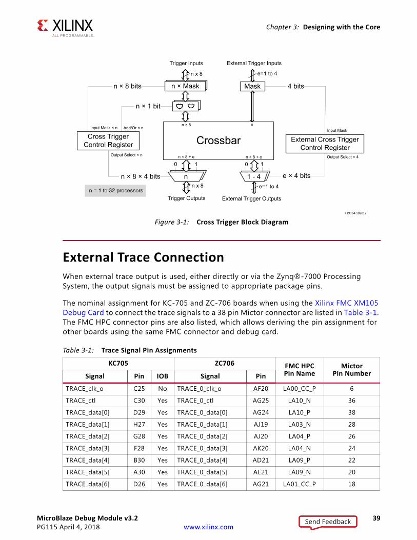
Cross Trigger ProgrammingThe MDM core provides a programmable cross trigger crossbar that allows the eight trigger inputs of each connected processor and the four external trigger inputs to affect each of the eight trigger outputs of each connected processor and four external trigger outputs.
IMPORTANT: In order to use the MDM core cross trigger functionality, all connected MicroBlaze processors must be configured to use Extended Debug (C_DEBUG_ENABLED = 2).
Send Feedback

MicroBlaze Debug Module v3.2 38PG115 April 4, 2018 www.xilinx.com
Chapter 3: Designing with the Core
In the simplest use case no programming is necessary, because the initial crossbar configuration is set up to:
• Connect the first four trigger inputs (Trigger Input 0 - 3) of the MicroBlaze processors to the external trigger outputs (External Trigger Output 0 - 3).
• Connect the external trigger inputs (External Trigger Input 0 - 3) to the first four trigger outputs (Trigger Output 0 - 3) of the MicroBlaze processors.
The parameter C_EXT_TRIG_RESET_VALUE can be used to change this behavior, by setting the reset value of the External Cross Trigger Control Debug register. See the MicroBlaze Processor Reference Guide (UG984) [Ref 5], for the definition of the MicroBlaze trigger inputs and outputs.
The crossbar is programmed per output and connected processor. The following sequence of debug register accesses can be used to select and program a trigger output of a specific MicroBlaze processor:
1. If there are more than one MicroBlaze processor, use the Which MicroBlaze Debug register (see Table 2-34) to select which processor to affect. If the trigger outputs of more than one processor in the crossbar should be connected the same way, all those processors can be selected for simultaneous write.
2. For each of the 8 trigger outputs to define, write the Cross Trigger Control register (see Table 2-38) with the appropriate value, setting the register Index field to the trigger output number.
3. For each of the 4 external trigger outputs to define, write the External Cross Trigger Control register (see Table 2-36) with the appropriate value, setting the register Index field to the external trigger output number.
To force a trigger output, a Cross Trigger Control register can be written twice, first to set the Output Select field to Static One, and then to restore the previous value.
The connection of the trigger inputs and outputs to the crossbar, and how they are affected by the cross trigger control registers is illustrated in Figure 3-1.
Send Feedback
MicroBlaze Debug Module v3.2 39PG115 April 4, 2018 www.xilinx.com
Chapter 3: Designing with the Core
External Trace ConnectionWhen external trace output is used, either directly or via the Zynq®-7000 Processing System, the output signals must be assigned to appropriate package pins.
The nominal assignment for KC-705 and ZC-706 boards when using the Xilinx FMC XM105 Debug Card to connect the trace signals to a 38 pin Mictor connector are listed in Table 3-1. The FMC HPC connector pins are also listed, which allows deriving the pin assignment for other boards using the same FMC connector and debug card.
X-Ref Target - Figure 3-1
Figure 3-1: Cross Trigger Block Diagram
Table 3-1: Trace Signal Pin Assignments
KC705 ZC706 FMC HPCPin Name
MictorPin NumberSignal Pin IOB Signal Pin
TRACE_clk_o C25 No TRACE_0_clk_o AF20 LA00_CC_P 6
TRACE_ctl C30 Yes TRACE_0_ctl AG25 LA10_N 36
TRACE_data[0] D29 Yes TRACE_0_data[0] AG24 LA10_P 38
TRACE_data[1] H27 Yes TRACE_0_data[1] AJ19 LA03_N 28
TRACE_data[2] G28 Yes TRACE_0_data[2] AJ20 LA04_P 26
TRACE_data[3] F28 Yes TRACE_0_data[3] AK20 LA04_N 24
TRACE_data[4] B30 Yes TRACE_0_data[4] AD21 LA09_P 22
TRACE_data[5] A30 Yes TRACE_0_data[5] AE21 LA09_N 20
TRACE_data[6] D26 Yes TRACE_0_data[6] AG21 LA01_CC_P 18
Mask
Trigger Inputs External Trigger Inputs
e × 4 bits
0 1
External Trigger Outputs
Mask 4 bits n × Mask
0 1
n × 8 bits
Trigger Outputs
n × 8 × 4 bits
Input Mask
Output Select × 4
External Cross Trigger Control Register
1 - 4
Cross TriggerControl Register
Output Select × n
Input Mask × n
Crossbar
n = 1 to 32 processors
Maskn × 1 bit
And/Or × n
n × 8 + e n × 8 + e
n × 8 e
n
X19934-102017
Send Feedback

MicroBlaze Debug Module v3.2 40PG115 April 4, 2018 www.xilinx.com
Chapter 3: Designing with the Core
For the KC-705 board, the IOB column indicates pins where it is recommended to add a constraint to place the output flip-flop in the pad to minimize skew. The parameter C_TRACE_OUTPUT should be set to 1 and C_TRACE_DATA_WIDTH should be set to 16 with this pin assignment.
For the ZC-706 board the MDM trace signals should be connected to the Zynq-7000 Processing System Fabric Trace Monitor (FTM), and the Zynq-7000 Processing System should be configured to output 16 data bits. The parameter C_TRACE_OUTPUT should be set to 2 in this case,
Protocol DescriptionThe MDM Debug protocol is Xilinx internal, and not described in this document. All the details of the protocol are handled transparently to the user by the Xilinx System Debugger (XSDB) or by the Software Development Kit (SDK) System Debugger.
TRACE_data[7] C26 Yes TRACE_0_data[7] AH21 LA01_CC_N 16
TRACE_data[8] G29 Yes TRACE_0_data[8] AH23 LA05_P 37
TRACE_data[9] F30 Yes TRACE_0_data[9] AH24 LA05_N 35
TRACE_data[10] H30 Yes TRACE_0_data[10] AG22 LA06_P 33
TRACE_data[11] G30 Yes TRACE_0_data[11] AH22 LA06_N 31
TRACE_data[12] E28 Yes TRACE_0_data[12] AJ23 LA07_P 29
TRACE_data[13] D28 Yes TRACE_0_data[13] AJ24 LA07_N 27
TRACE_data[14] E29 Yes TRACE_0_data[14] AF19 LA08_P 25
TRACE_data[15] E30 Yes TRACE_0_data[15] AG19 LA08_N 23
Logic 0 = 0V H26 No Logic 0 = 0V AH19 LA03_P 30
Logic 0 = 0V H25 No Logic 0 = 0V AK18 LA02_N 32
Logic 1 = 1.8V H24 No Logic 1 = 1.8V AK17 LA02_P 34
Table 3-1: Trace Signal Pin Assignments (Cont’d)
KC705 ZC706 FMC HPCPin Name
MictorPin NumberSignal Pin IOB Signal Pin
Send Feedback

MicroBlaze Debug Module v3.2 41PG115 April 4, 2018 www.xilinx.com
Chapter 4
Design Flow StepsThis chapter describes customizing and generating the core, constraining the core, and the simulation, synthesis and implementation steps that are specific to this IP core. More detailed information about the standard Vivado® design flows and the IP integrator can be found in the following Vivado Design Suite user guides:
• Vivado Design Suite User Guide: Designing IP Subsystems using IP Integrator (UG994) [Ref 8]
• Vivado Design Suite User Guide: Designing with IP (UG896) [Ref 9]
• Vivado Design Suite User Guide: Getting Started (UG910) [Ref 10]
• Vivado Design Suite User Guide: Logic Simulation (UG900) [Ref 11]
Customizing and Generating the CoreThis section includes information about using Xilinx® tools to customize and generate the core in the Vivado® Design Suite.
If you are customizing and generating the core in the Vivado IP Integrator, see the Vivado Design Suite User Guide: Designing IP Subsystems using IP Integrator (UG994) [Ref 8] for detailed information. IP Integrator might auto-compute certain configuration values when validating or generating the design. To check whether the values do change, see the description of the parameter in this chapter. To view the parameter value, run the validate_bd_design command in the Tcl console.
You can customize the IP for use in your design by specifying values for the various parameters associated with the IP core using the following steps:
1. Select the IP from the IP catalog.
2. Double-click the selected IP or select the Customize IP command from the toolbar or right-click menu.
For details, see the Vivado Design Suite User Guide: Designing with IP (UG896) [Ref 9] and the Vivado Design Suite User Guide: Getting Started (UG910) [Ref 10].
IMPORTANT: When using MicroBlaze parallel debug access, you must manually change the MDM address range from 4K to 64K in the Vivado IP Integrator Address Editor.
Send Feedback

MicroBlaze Debug Module v3.2 42PG115 April 4, 2018 www.xilinx.com
Chapter 4: Design Flow Steps
Note: Figures in this chapter are illustrations of the Vivado IDE. The layout depicted here might vary from the current version.
The MDM core parameters are divided into three categories: Debug, UART and Advanced. When using the Vivado IP Integrator, the address for the JTAG-based UART is auto-generated.
The Customize IP dialog box is shown in Figure 4-1.
• Number of MicroBlaze debug ports - Sets the number of ports available to connect to MicroBlaze processors.
• Enable Debug Register Access From AXI - Enables the functionality to access JTAG Debug registers from AXI and the AXI4-Lite slave interface.
X-Ref Target - Figure 4-1
Figure 4-1: Customize IP Dialog Box
Send Feedback

MicroBlaze Debug Module v3.2 43PG115 April 4, 2018 www.xilinx.com
Chapter 4: Design Flow Steps
• Enable AXI Memory Access From Debug - Enables the functionality to access memory directly from JTAG, using the AXI4 master interface and the LMB master interfaces.
• Enable Cross Trigger - Enables the cross trigger functionality, and the external cross-trigger interfaces. Cross trigger is not available when selecting AXI parallel debug.
• Enable JTAG UART - Enables the JTAG UART and the AXI4-Lite slave interface to access the UART registers.
• Select External Trace Output Interface - Enables trace output functionality, and selects the output interface: External, AXI4-Stream or AXI4-Master. External trace is not available when selecting AXI parallel debug.
• External Trace Data Width - Defines the data width for the trace output interface External and AXI4-Stream: 2, 4, 8, 16 or 32 bits.
• Specify the JTAG user-defined register used - Select JTAG user-defined register. Can be set to USER1, USER2, USER3 or USER4. Should never need to be changed from USER2, unless there is a conflict with another IP core in the system.
• Select BSCAN location - Selects whether internal or external BSCAN is used, or disables BSCAN. Should normally be set to INTERNAL in an embedded system. Should be set to EXTERNAL or EXTERNAL HIDDEN when debugging with the Xilinx Virtual Cable (XVC) using the Debug Bridge. Can be set to NONE to disable BSCAN completely, when only Debug register access is used and no software debug is required.
• Number of External Trigger Inputs - Defines the number of external trigger input interfaces to use when cross trigger is enabled.
• Number of External Trigger Outputs - Defines the number of external trigger output interfaces to use when cross trigger is enabled.
Parameter ValuesTo tailer an MDM core uniquely for a specific system, certain features can be parameterized in the core design. This allows you to configure a design that only utilizes the resources required by the system. The features that can be parameterized in MDM designs are shown in Table 4-1.
Send Feedback

MicroBlaze Debug Module v3.2 44PG115 April 4, 2018 www.xilinx.com
Chapter 4: Design Flow Steps
Table 4-1: MDM Design Parameters
Feature / Description Parameter Name Allowable Values DefaultValue
VHDLType
System Parameters
Target family C_FAMILY See LogiCORE™ IP Facts Table virtex7 string
Debug Parameters
Number of MicroBlaze debug ports C_MB_DBG_PORTS 0–32(1) 1 integer
Enable Debug register access from AXI C_DBG_REG_ACCESS 0,1 0 integer
Enable AXI memory access from debug C_DBG_MEM_ACCESS 0,1 0 integer
Enable cross trigger(3) C_USE_CROSS_TRIGGER 0,1 0 integer
UART Parameters
Enable JTAG UART C_USE_UART 0,1 1 integer
Trace Parameters(3)
Enable Trace Output C_TRACE_OUTPUT 0,1,2,3 0 integer
External and AXI4-Stream Trace Data Width C_TRACE_DATA_WIDTH 2,4,8,16,32 0 integer
External Trace Clock Input Frequency(2) C_TRACE_CLK_FREQ_HZ
Output clock frequencymultiplied by 2
200 integer
External Trace Clock Phase(2) C_TRACE_CLK_OUT_PHASE 0–360 90 integer
External Trace Protocol(2) C_TRACE_PROTOCOL 0 = DEFAULT1 = ALTERNATE 1 integer
External Trace ID(2) C_TRACE_ID 1–110 110 integer
Advanced Parameters
Specifies the JTAGuser-defined register used C_JTAG_CHAIN
1 = USER12 = USER23 = USER34 = USER4
2 integer
Select BSCAN location C_USE_BSCAN
0 = INTERNAL2 = EXTERNAL3 = NONE4 = EXTERNAL HIDDEN
0 integer
Define BSCAN id(2) C_BSCANID 0 - 0xFFFFFFFF 0x4900300 integer
MicroBlaze Debug connection(2) C_DEBUG_INTERFACE
0 = SERIAL1 = PARALLEL2 = AXI
0 integer
Number of external trigger inputs C_TRIG_IN_PORTS 0,1,2,3,4 1 integer
Send Feedback

MicroBlaze Debug Module v3.2 45PG115 April 4, 2018 www.xilinx.com
Chapter 4: Design Flow Steps
In addition to the parameters listed in this table, there are also parameters that are inferred for each AXI interface in the tools. Through the design, these inferred parameters control the behavior of the AXI Interconnect. For a complete list of the interconnect settings related to the AXI interface, see the LogiCORE AXI Interconnect IP Product Guide (PG059) [Ref 12].
User ParametersTable 4-2 shows the relationship between the fields in the Vivado IDE and the User Parameters (which can be viewed in the Tcl console).
Allowable Parameter CombinationsThere are no restrictions on parameter combinations for this core.
Number of external trigger outputs C_TRIG_OUT_PORTS 0,1,2,3,4 1 integer
External trigger reset value(2) C_EXT_TRIG_RESET_VALUE 0x00000–0xFFFFF 0xF1234 integer
Avoid SRL16 and SRL32 FPGA primitives(2) C_AVOID_PRIMITIVES 0,1 0 integer
Notes: 1. A value of 0 is legal and can be used if the MDM core is set up to only access AXI memory.2. Not available in the Customize IP dialog box.3. Not available when C_DEBUG_INTERFACE = 2 (AXI).
Table 4-2: Vivado IDE Parameter to User Parameter Relationship
Vivado IDE Parameter User Parameter Default Value
Number of MicroBlaze debug ports C_MB_DBG_PORTS 1
Enable Debug Register Access from AXI C_DBG_REG_ACCESS 0
Enable AXI Memory Access From Debug C_DBG_MEM_ACCESS 0
Enable Cross Trigger C_USE_CROSS_TRIGGER 0
Enable JTAG UART C_USE_UART 0
Select External Trace Output Interface C_TRACE_OUTPUT 0 = None
External Trace Data Width C_TRACE_DATA_WIDTH 32
Specifies the JTAG user-defined register used C_JTAG_CHAIN 2 = USER2
Select BSCAN location C_USE_BSCAN 0 = INTERNAL
Number of External Trigger Inputs C_TRIG_IN_PORTS 1
Number of External Trigger Outputs C_TRIG_OUT_PORTS 1
Table 4-1: MDM Design Parameters (Cont’d)
Feature / Description Parameter Name Allowable Values DefaultValue
VHDLType
Send Feedback

MicroBlaze Debug Module v3.2 46PG115 April 4, 2018 www.xilinx.com
Chapter 4: Design Flow Steps
Output GenerationThe following files are generated by the IP in Vivado IP Integrator:
• Verilog/VHDL Template
• VHDL source files
• VHDL wrapper file in the library work
For details, see the Vivado Design Suite User Guide: Designing with IP (UG896) [Ref 9].
Constraining the CoreThis section contains information about constraining the core in the Vivado Design Suite.
Required ConstraintsThis section is not applicable for this IP core.
Device, Package, and Speed Grade SelectionsThis section is not applicable for this IP core.
Clock FrequenciesThis section is not applicable for this IP core.
Clock ManagementThe MDM Debug logic is fully synchronous with the BSCAN module. Internally BUFG primitives are instantiated to buffer the DRCK clock from the BSCAN module.
The MDM JTAG-based UART and Debug register access is fully synchronous to the AXI4-Lite slave bus interface clock, and isolated from the BSCAN clock region with FIFOs and synchronization flip-flops when BSCAN is used.
The JTAG Memory Access AXI4 master interface and LMB master interfaces are fully synchronous to the AXI4 master clock, and isolated from the BSCAN clock region with FIFOs and synchronization flip-flops.
When MicroBlaze parallel debug interface is selected (C_DEBUG_INTERFACE > 0) all Debug register access is fully synchronous to the AXI4-Lite slave bus interface clock. The clocking of the connected processors depends on the used interface:
• In case C_DEBUG_INTERFACE is set to 1 (PARALLEL), the same clock must be used to clock the AXI4-Lite slave bus interface and all connected MicroBlaze processors.
Send Feedback

MicroBlaze Debug Module v3.2 47PG115 April 4, 2018 www.xilinx.com
Chapter 4: Design Flow Steps
• In case C_DEBUG_INTERFACE is set to 2 (AXI), different clocks can be used by the MDM and the connected MicroBlaze processors, since the AXI interconnect provides clock conversion.
Clock PlacementThis section is not applicable for this IP core.
BankingThis section is not applicable for this IP core.
Transceiver PlacementThis section is not applicable for this IP core.
I/O Standard and PlacementThis section is not applicable for this IP core.
SimulationFor comprehensive information about Vivado simulation components, as well as information about using supported third-party tools, see the Vivado Design Suite User Guide: Logic Simulation (UG900) [Ref 11].
IMPORTANT: For cores targeting 7 series or Zynq-7000 devices, UNIFAST libraries are not supported. Xilinx IP is tested and qualified with UNISIM libraries only.
Synthesis and ImplementationFor details about synthesis and implementation, see the Vivado Design Suite User Guide: Designing with IP (UG896) [Ref 9].
Send Feedback
MicroBlaze Debug Module v3.2 48PG115 April 4, 2018 www.xilinx.com
Appendix A
UpgradingThis appendix contains information about migrating a design from the ISE® Design Suite to the Vivado® Design Suite, and for upgrading to a more recent version of the IP core. For customers upgrading in the Vivado Design Suite, important details (where applicable) about any port changes and other impact to user logic are included.
Migrating to the Vivado Design SuiteFor information about migrating to the Vivado Design Suite, see the ISE to Vivado Design Suite Migration Guide (UG911) [Ref 13].
Upgrading in the Vivado Design SuiteThis section provides information about any changes to the user logic or port designations that take place when you upgrade to a more current version of this IP core in the Vivado Design Suite.
The AXI4-Lite slave interface address width parameter, C_S_AXI_ADDR_WIDTH, has been changed to only use the necessary number of bits to decode the AXI slave registers. The parameter is normally automatically determined, and need not be explicitly set.
Send Feedback

MicroBlaze Debug Module v3.2 49PG115 April 4, 2018 www.xilinx.com
Appendix B
DebuggingThis appendix includes details about resources available on the Xilinx Support website and debugging tools.
Finding Help on Xilinx.comTo help in the design and debug process when using the MDM core, the Xilinx Support web page contains key resources such as product documentation, release notes, answer records, information about known issues, and links for obtaining further product support.
DocumentationThis product guide is the main document associated with the MDMcore. This guide, along with documentation related to all products that aid in the design process, can be found on the Xilinx Support web page or by using the Xilinx® Documentation Navigator.
Download the Xilinx Documentation Navigator from the Downloads page. For more information about this tool and the features available, open the online help after installation.
Answer Records Answer Records include information about commonly encountered problems, helpful information on how to resolve these problems, and any known issues with a Xilinx product. Answer Records are created and maintained daily ensuring that users have access to the most accurate information available.
Answer Records for this core can be located by using the Search Support box on the main Xilinx support web page. To maximize your search results, use proper keywords such as
• Product name
• Tool message(s)
• Summary of the issue encountered
A filter search is available after results are returned to further target the results.
Send Feedback

MicroBlaze Debug Module v3.2 50PG115 April 4, 2018 www.xilinx.com
Appendix B: Debugging
Master Answer Record for the MDM Core
AR: 54413
Technical SupportXilinx provides technical support at the Xilinx Support web page for this LogiCORE™ IP product when used as described in the product documentation. Xilinx cannot guarantee timing, functionality, or support if you do any of the following:
• Implement the solution in devices that are not defined in the documentation.
• Customize the solution beyond that allowed in the product documentation.
• Change any section of the design labeled DO NOT MODIFY.
To contact Xilinx Technical Support, navigate to the Xilinx Support web page.
Debug ToolsThe main tool available to address MDM design issues is the Vivado® Design Suite debug feature.
Vivado Design Suite Debug FeatureThe Vivado Design Suite debug feature inserts logic analyzer and virtual I/O cores directly into your design. The debug feature also allows you to set trigger conditions to capture application and integrated block port signals in hardware. Captured signals can then be analyzed. This feature in the Vivado IDE is used for logic debugging and validation of a design running in Xilinx devices.
The Vivado logic analyzer is used with the logic debug IP cores, including:
• ILA 2.0 (and later versions)
• VIO 2.0 (and later versions)
See the Vivado Design Suite User Guide: Programming and Debugging (UG908) [Ref 14].
Reference BoardsAll 7 series and UltraScale™ architecture Xilinx development boards support the MDM core. These boards can be used to prototype designs and establish that the core can communicate with the system.
Send Feedback

MicroBlaze Debug Module v3.2 51PG115 April 4, 2018 www.xilinx.com
Appendix B: Debugging
Simulation DebugThe simulation debug flow for Mentor Graphics Questa Advanced Simulator is described below. A similar approach can be used with other simulators.
• Check for the latest supported versions of Questa Advanced Simulator in the Xilinx Design Tools: Release Notes Guide. Is this version being used? If not, update to this version.
• If using Verilog, do you have a mixed mode simulation license? If not, obtain a mixed-mode license.
• Ensure that the proper libraries are compiled and mapped. In the Vivado Design Suite Flow > Simulation Settings can be used to define the libraries.
• Have you associated the intended software program for the MicroBlaze™ processor with the simulation? Use the command Tools > Associate ELF Files in Vivado Design Suite.
• When observing the traffic on the interfaces connected to the MDM core, see the timing in the relevant specification:
° For AXI4 and AXI4-Lite, see the AMBA® AXI and ACE Protocol Specification [Ref 1].
Hardware DebugHardware issues can range from link bring-up to problems seen after hours of testing. This section provides debug steps for common issues. The Vivado Design Suite debug feature is a valuable resource to use in hardware debug. The signal names mentioned in the following sections can be probed using the debug feature to debug specific problems.
Many of these common issues can also be applied to debugging design simulations.
General ChecksEnsure that all the timing constraints for the core were properly incorporated from the example design and that all constraints were met during implementation.
• Does it work in post-place and route timing simulation? If problems are seen in hardware but not in timing simulation, this could indicate a PCB issue. Ensure that all clock sources are active and clean.
• If using MMCMs in the design, ensure that all MMCMs have obtained lock by monitoring the locked port.
Send Feedback

MicroBlaze Debug Module v3.2 52PG115 April 4, 2018 www.xilinx.com
Appendix B: Debugging
AXI4-Lite Slave Interface DebugRead from a register that does not have all 0s as a default to verify that the interface is functional. Output S_AXI_ARREADY asserts when the read address is valid, and output S_AXI_RVALID asserts when the read data/response is valid. If the interface is unresponsive, ensure that the following conditions are met:
• The S_AXI_ACLK input is connected and toggling.
• The interface is not being held in reset, and S_AXI_ARESETN is an active-Low reset.
• If the simulation has been run, verify in simulation and/or a debug feature capture that the waveform is correct for accessing the AXI4-Lite interface.
Send Feedback
MicroBlaze Debug Module v3.2 53PG115 April 4, 2018 www.xilinx.com
Appendix C
Application Software Development
Device DriversThe MDM JTAG-based UART interface is supported by the UART Lite driver, included with Xilinx Software Development Kit.
Send Feedback

MicroBlaze Debug Module v3.2 54PG115 April 4, 2018 www.xilinx.com
Appendix D
Additional Resources and Legal Notices
Xilinx ResourcesFor support resources such as Answers, Documentation, Downloads, and Forums, see Xilinx Support.
Documentation Navigator and Design HubsXilinx® Documentation Navigator provides access to Xilinx documents, videos, and support resources, which you can filter and search to find information. To open the Xilinx Documentation Navigator (DocNav):
• From the Vivado® IDE, select Help > Documentation and Tutorials.
• On Windows, select Start > All Programs > Xilinx Design Tools > DocNav.
• At the Linux command prompt, enter docnav.
Xilinx Design Hubs provide links to documentation organized by design tasks and other topics, which you can use to learn key concepts and address frequently asked questions. To access the Design Hubs:
• In the Xilinx Documentation Navigator, click the Design Hubs View tab.
• On the Xilinx website, see the Design Hubs page.
Note: For more information on Documentation Navigator, see the Documentation Navigator page on the Xilinx website.
Send Feedback

MicroBlaze Debug Module v3.2 55PG115 April 4, 2018 www.xilinx.com
Appendix D: Additional Resources and Legal Notices
ReferencesThese documents provide supplemental material useful with this user guide:
1. AMBA AXI and ACE Protocol Specification (ARM IHI 0022E)
2. AMBA AXI4-Stream Protocol Specification. Version 1.0 (ARM IHI 0051A)
3. ARM CoreSight Architecture Specification, v2.0 (ARM IHI 0029D)
4. LogiCORE IP AXI UART Lite Product Guide (PG142)
5. MicroBlaze Processor Reference Guide (UG984)
6. LogiCORE IP LMB BRAM Interface Controller Product Guide (PG112)
7. Zynq-7000 All Programmable SoC, Technical Reference Manual (UG585)
8. Vivado Design Suite User Guide: Designing IP Subsystems using IP Integrator (UG994)
9. Vivado Design Suite User Guide, Designing with IP (UG896)
10. Vivado Design Suite User Guide: Getting Started (UG910)
11. Vivado Design Suite User Guide: Logic Simulation (UG900)
12. LogiCORE AXI Interconnect IP Product Guide (PG059)
13. ISE® to Vivado® Design Suite Migration Methodology Guide (UG911)
14. Vivado Design Suite User Guide: Programming and Debugging (UG908)
15. Debug Bridge LogiCORE IP Product Guide (PG245)
Send Feedback

MicroBlaze Debug Module v3.2 56PG115 April 4, 2018 www.xilinx.com
Appendix D: Additional Resources and Legal Notices
Revision History The following table shows the revision history for this document.
Date Version Revision
04/04/2018 3.2 • Describe feature to locate MDM with internal BSCAN in Master SLR.
• Updated description of parallel debug clocking.
12/20/2017 3.2 • Documented that MDM always responds to AXI slave accesses.
• Added description of alternate external trace protocol.
• Described external cross trigger reset value parameter.
10/04/2017 3.2 • Updated description of parallel debug access.
• Added description of Xilinx Virtual Cable (XVC) support.
• Added bscan_ext_tck port.
04/05/2017 3.2 • Added description of parameter to control instantiation of FPGA primitives.
• Updated external trace to describe option to set AXI4-Stream data width.
10/05/2016 3.2 • Added description of parallel debug access.
• Replaced references to the deprecated Xilinx Microprocessor Debugger (XMD) with Xilinx System Debugger (XSDB).
11/18/2015 3.2 Added support for UltraScale+ families.
06/24/2015 3.2 Moved performance and resource utilization data to the web.
10/01/2014 3.2 • Updated due to core revision.
• Added description of external trace.
04/02/2014 3.1 • Document version number advanced to match the core version number.
• Updated due to core revision.
• Added description of debug enhancements.
03/20/2013 1.0 This Product Guide replaces PG062. There are no documentation changes for this release.
Send Feedback

MicroBlaze Debug Module v3.2 57PG115 April 4, 2018 www.xilinx.com
Appendix D: Additional Resources and Legal Notices
Please Read: Important Legal NoticesThe information disclosed to you hereunder (the “Materials”) is provided solely for the selection and use of Xilinx products. To the maximum extent permitted by applicable law: (1) Materials are made available “AS IS” and with all faults, Xilinx hereby DISCLAIMS ALL WARRANTIES AND CONDITIONS, EXPRESS, IMPLIED, OR STATUTORY, INCLUDING BUT NOT LIMITED TO WARRANTIES OF MERCHANTABILITY, NON-INFRINGEMENT, OR FITNESS FOR ANY PARTICULAR PURPOSE; and (2) Xilinx shall not be liable (whether in contract or tort, including negligence, or under any other theory of liability) for any loss or damage of any kind or nature related to, arising under, or in connection with, the Materials (including your use of the Materials), including for any direct, indirect, special, incidental, or consequential loss or damage (including loss of data, profits, goodwill, or any type of loss or damage suffered as a result of any action brought by a third party) even if such damage or loss was reasonably foreseeable or Xilinx had been advised of the possibility of the same. Xilinx assumes no obligation to correct any errors contained in the Materials or to notify you of updates to the Materials or to product specifications. You may not reproduce, modify, distribute, or publicly display the Materials without prior written consent. Certain products are subject to the terms and conditions of Xilinx's limited warranty, please refer to Xilinx's Terms of Sale which can be viewed at https://www.xilinx.com/legal.htm#tos; IP cores may be subject to warranty and support terms contained in a license issued to you by Xilinx. Xilinx products are not designed or intended to be fail-safe or for use in any application requiring fail-safe performance; you assume sole risk and liability for use of Xilinx products in such critical applications, please refer to Xilinx's Terms of Sale which can be viewed at https://www.xilinx.com/legal.htm#tos.AUTOMOTIVE APPLICATIONS DISCLAIMERAUTOMOTIVE PRODUCTS (IDENTIFIED AS “XA” IN THE PART NUMBER) ARE NOT WARRANTED FOR USE IN THE DEPLOYMENT OF AIRBAGS OR FOR USE IN APPLICATIONS THAT AFFECT CONTROL OF A VEHICLE (“SAFETY APPLICATION”) UNLESS THERE IS A SAFETY CONCEPT OR REDUNDANCY FEATURE CONSISTENT WITH THE ISO 26262 AUTOMOTIVE SAFETY STANDARD (“SAFETY DESIGN”). CUSTOMER SHALL, PRIOR TO USING OR DISTRIBUTING ANY SYSTEMS THAT INCORPORATE PRODUCTS, THOROUGHLY TEST SUCH SYSTEMS FOR SAFETY PURPOSES. USE OF PRODUCTS IN A SAFETY APPLICATION WITHOUT A SAFETY DESIGN IS FULLY AT THE RISK OF CUSTOMER, SUBJECT ONLY TO APPLICABLE LAWS AND REGULATIONS GOVERNING LIMITATIONS ON PRODUCT LIABILITY.© Copyright 2013–2018 Xilinx, Inc. Xilinx, the Xilinx logo, Artix, ISE, Kintex, Spartan, Virtex, Vivado, Zynq, and other designated brands included herein are trademarks of Xilinx in the United States and other countries. AMBA, AMBA Designer, ARM, ARM1176JZ-S, CoreSight, Cortex, PrimeCell, and MPCore are trademarks of ARM in the EU and other countries. All other trademarks are the property of their respective owners.
Send Feedback