Embed Size (px)
Citation preview

AN1529Microchip M2M Development Platform for CDMA
Machine-to-Machine (M2M) technology allows remotedevices to communicate with each other or with a cen-tral server over one or more communications networks.M2M is commonly used to monitor or control devicesdeployed at remote locations without the need ofhuman assistance. M2M is used in a wide variety ofapplications, such as utility meters, asset tracking,robotics, supply chain management and many others.
The Microchip M2M Development Platform for CDMAuses the Verizon Wireless cellular network tocommunicate with a cloud-based server. Cellular-based technology is ideal for M2M, as it can provide acommon communication pathway for remote andmobile devices to exchange information.
The Microchip M2M platform provides a variety ofsensors and communications technologies to interfacewith remote devices. The platform sends and receivesdata to and from a cloud-based server through theCDMA cellular network. The server is accessed by theuser through a web portal that can be customized to anindividual user's needs. Through the web portal, theuser can display, analyze and download data collectedby the M2M platform, and send commands to theplatform to control remote devices.
THE M2M ECOSYSTEM
The Microchip M2M Development Platform for CDMAmakes it easy to learn and develop M2M solutions thatcommunicate over the Verizon Wireless network. Theplatform is one part of an integrated, cloud-based M2Mecosystem. The platform communicates with theecosystem through the Verizon Wireless CDMAcellular network. Data is sent and received through aVerizon cloud-based M2M data management center.Data received by Verizon is forwarded to a cloud-baseddata server where it is stored in a database. Thecontents of the database are accessible through anyweb browser that has access to the Internet. Throughthis web portal, users can monitor and control anynumber of M2M devices.
FIGURE 1: PIC32-BASED M2M ECOSYSTEM (HTML5/VERIZON WIRELESS)
Twisthink Web Server
Verizon Wireless
Internet
Developer GUI
VerizonAdvanced
M2M
Cellular TowerM2M Platform
Hosted Private Network (HPN)
2013 Microchip Technology Inc. DS00001529A-page 1

AN1529
FEATURE OVERVIEW
The Microchip M2M Development Platform for CDMAprovides a Verizon Wireless-certified “out-of-the-box”M2M solution, or can be used as an extensible platformfor custom applications. The platform provides a varietyof sensors and interfaces to allow the designer to tailorthe solution for a specific application.
The M2M platform RF software and hardware arecertified under the Verizon Wireless OpenDevelopment Initiative (ODI) certificationspecifications, and have been approved for use on theVerizon Wireless network. The application softwarecommunicates to the network using the Verizon DeviceClient Framework (DCF). The DCF softwareimplementation is owned by Verizon, and is providedwith the platform as a binary module. Documentationfor the DCF API is available from the Microchip M2Mweb site. Refer to “Verizon M2M DeveloperProgram” for more information.
The DCF binary module and source code for theapplication software is available for download from theMicrochip web site at www.microchip.com/m2m.
Figure 2 provides a hardware block diagram of theMicrochip M2M Development Platform for CDMA.
Certifications
The Microchip M2M Development Platform for CDMA(P/N: DM320017) is a development/evaluation tooldesigned to be used for research and development ina laboratory environment to enable customers toexperiment with software to develop their target end-products. The DM320017 is certified as FCC Part 15compliant for use as a finished product in the UnitedStates and Canada.
The DM320017 carries the CE label for compliancewith EU Directive 2011/65/EU (RoHS2). It should notbe placed into the EU market (e.g., sale, loan, lease,gift, etc.) without confirmation of inapplicability of oralternatively, compliance to, EU EMC Directive 2004/108/EC as supported by the European Commission’sGuide for the EMC Directive 2004/108/EC(8th February 2010).
See Appendix D: “RF Exposure Information” forFCC and RSS certification information.
Programming Support
FIRMWARE UPDATES
The M2M platform provides a Microchip In-CircuitSystem Programming (ICSP) debugger/programmerinterface (J9) for physically connecting a MicrochipMPLAB® REAL ICE™ In-Circuit Emulator or MPLABICD 3 In-Circuit Debugger to update the firmware inthe host PIC32 microcontroller. See Appendix B:“Referenced Sources” for information on obtainingthese development tools.
Power Supply
INPUT
The M2M platform is powered by a 12V DC, 500 mApower supply, which is included with the platform.
OUTPUT
12V DC input power and 3.3V DC regulated I/O powerare available on the General Purpose I/O header topower external devices.
Operating Temperature
All functions of the M2M platform operate betweenthe temperature range of -20ºC and +85°C (batteriesmay not meet this requirement).
DS00001529A-page 2 2013 Microchip Technology Inc.

2
01
3 M
icroch
ip T
ech
no
log
y Inc.
DS
00
00
15
29
A-p
ag
e 3
AN
1529
FIG
NovatelHS3001 CDMA
FCC ID: MIVCNN0301
micro-USB
Front-End Modulealun
Dual-band Cellular Antenna
Filter
Light Sensor
Accelerometer
Temperature Sensor
Slot Antenna
Filter
Coax
Coax
GPS u-bloxMAX-6Q LNA/SW
Filter
Coax
GPS Antenna
URE 2: HARDWARE BLOCK DIAGRAM
Power Supply
3.8V Step Down Regulator
Connectors
Debug Header
Power Adapter Input (6V-24V)
I/O Headers(2 x 10-pin)
UART
USB On-The-Go
micro-B USB
ICSP™ Pins
User Interface
Power LEDs
Cellular Signal LEDs
3.3V LDO
3.3V
Programmable I/O
5V Step Down Regulator
Cell Power
UART
RS-232 Level Shifter
RS232(DB9)
Cellular Activity LEDs
Status LEDs
GPIO
PWM SPI
Analog Digital
UART
CAN
CAN Transceiver
CAN(DB9)
802.15.4 Transceiver B
SPI
8 Mb Flash Memory
SPI
512 KB Flash 128 KB Data Memory
80 MHz Core Processor
20 MHz Crystal
Microcontroller PIC32MX795F512L
GPIO
5V DC Output
Ethernet
Ethernet PHY
RJ-45
ADC
I2C™
SD Card
SPI
UART
20 MHz
1 MHz Switching
2.25 MHz Switching
Cell Power
20 M
Hz
25 MHz

AN1529
HARDWARE DESCRIPTION
M2M Development Board
The top assembly of the board includes these keyfeatures, as indicated in Figure 3:
1. Multi-band antenna (E1).
2. GPS module (U4).
3. micro-USB connector (J8).
4. Microchip PIC32MX795F512L microcontroller (U8).
5. MPLAB REAL ICE in-circuit emulatorprogrammer port (J9).
6. Ethernet 802.3 RJ-45 connector (J7).
7. Standard micro-USB connector (J3).
8. RS-232 DB9 connector (J11).
9. LED 4 (green) (D12).
10. General purpose header 1 of 2 dual row, .100CTC, 10-pin connector (TB1).
11. General purpose header 2 of 2 dual row, .100CTC, 10-pin connector (TB2).
12. LED 3 (dual red and green) (D15).
13. Dual binary switch 6 (SW6).
14. Dual binary switch 5 (SW5).
15. LED 2 (red) (D14).
16. Dual binary switch 4 (SW4).
17. LED 1 (yellow) (D13).
18. Dual binary switch 3 (SW3).
19. Light sensor (U18).
20. Barrel type power adapter, 6-12V, 0.5 amp(J12).
21. Switch 2 – diagnostic mode button (SW2).
22. Switch 1 – reset button (SW1).
23. Triple axis accelerometer (U7).
24. Microchip 2.4 GHz transceiver (U2).
25. Microchip temperature sensor (U14).
FIGURE 3: M2M DEVELOPMENT BOARD COMPONENTS
20 1910 11
4
2
1
3
5
6
7
8912
1314
15
16
17
18
22
21
23
24
25
DS00001529A-page 4 2013 Microchip Technology Inc.

AN1529
General Purpose I/O Header
The General Purpose I/O Header (see Figure 4)provides two ADC connections to the external header,four general purpose digital I/O connections, one SPIconnection, and one UART connection. There is asingle power output that supplies 100 mA of current at3.3V DC and there is one ground connection to thecircuit board. In addition, the processor provides onePWM output on the external header.
FIGURE 4: GENERAL PURPOSE I/O (GPIO) HEADER
TABLE 1: GPIO PIN DESCRIPTIONS
8 7 6 5 4 3 2 1 16 15 14 13 12 11 10 9
Pin ID Signal Description
1 — I/O Power
2 U2TX External TX 485A
3 U2RX External RX 485B
4 SCK2 (see SW4 in Table 4) External Serial Clock
5 SDI2 (see SW4 in Table 4) External MISO
6 SDO2 (see SW3 in Table 4) External MOSI
7 Digital I/O or power out (see SW3 in Table 4) External GPIO or 12V Out
8 Ground Signal Ground
9 Digital I/O(1,3) External GPIO 1
10 Digital I/O(1,4) External GPIO 2
11 Digital I/O(1,3) External GPIO 3
12 Digital I/O(1) External GPIO 4
13 CTS(2) Clear-to-Send
14 RTS(2) Request-to-Send
15 AN8 Analog Input 1
16 AN9 Analog Input 2
Note 1: This signal is routed through an ST2149 bidirectional level shifter.
2: Due to pin allocation limitations, CTS and RTS must be implemented in software. If hardware flow control is not required, these pins can be used as additional GPIO.
3: This signal may be configured as an Output Compare for PWM generation.
4: This signal may be configured as a Change Notification input.
2013 Microchip Technology Inc. DS00001529A-page 5

AN1529
Figure 5 shows the UART2 signal logic flow based onthe settings of switch 5 and switch 6, as described inthe Communications Truth Table (see Table 5).
FIGURE 5: TRUTH TABLE DIAGRAM
MCU
232
485
Pass-Through
DB9
TB1
TX
TX
RX
TX
TX
RX
RX
U2TXR
DIN1
SW5
ROUT1
DU2RXA
B EXT_TX
EXT_RX
MCU
232
485
Pass-through
DB9
TB1
TX
TX
RX
TX
TX
RX
RX
U2TXR
DIN1
ROUT1
DU2RXA
B EXT_TX
EXT_RX
MCU
232
485
Pass-through
DB9
TB1
TX
TX
RX
TX
TX
RX
RX
U2TXR
DIN1
ROUT1
DU2RXA
B EXT_TX
EXT_RX
A=1
B=1
A = 0
B = 1
SW6
A = 0
B = 0
A = 0
B = 0
A = 1
B = 0
A = 1
B = 1
SW5
SW6
SW5
SW6
Indirectly ConnectedIntended Connection
DS00001529A-page 6 2013 Microchip Technology Inc.

AN1529
Figure 6 shows the right side of the platform and thelocations of the serial, RJ-45 Ethernet, and USBconnectors.
FIGURE 6: SERIAL, RJ-45 ETHERNET, AND USB CONNECTORS
Figure 7 shows the power adapter and microSD cardslot, and General Purpose I/O header.
FIGURE 7: POWER ADAPTER, SD CARD SLOT, AND EXTERNAL CONNECTIONS
2013 Microchip Technology Inc. DS00001529A-page 7

AN1529
User Interface
LED INDICATORS
The platform has four LED indicators. LEDs 1, 2, and 3(D13, D14, and D15) are controlled through software.LED4 (D12) is controlled by the cell module and is notavailable to the software.
TABLE 2: LED INDICATORS
PUSH BUTTONS
The platform features two push buttons that aremounted on the board. The operation of the pushbuttons is described in Table 3.
TABLE 3: PUSH BUTTONS
TABLE 4: DIP SWITCHES
TABLE 5: COMMUNICATIONS TRUTH TABLE
Name ID Description
LED 1 D13 Single color yellow LED.
LED 2 D14 Single color red LED.
LED 3 D15 Dual color LED (red and green).
LED 4 D12 Single color green LED.
Name ID Description
Button 1 SW1 Push button used to reset the PIC32 microcontroller.
Button 2 SW2 Push this button on power-up to force the M2M platform into Test mode (see Appendix E: “Board Layout and Sche-matics”).
ID Description
SW3 SW3A is used in combination with SW4 (see SW4 for further information).SW3B is used to select whether GPIO or 12V out is enabled on pin 7 of TB1.
SW4 Pole A of SW3 and poles A and B of SW4 are used together to select whether Ether-net or the SPI2 module is available at TB1.
SW5 SW5 used in combination with SW6 (see SW6 for further information).
SW6 SW6 is used in combination with SW5 to select the RS-232/RS-485 options (see Table 5).
Note: Due to pin limitations, the PIC32microcontroller can be configured toenable either the Ethernet module or theSPI2 module, but not both at the sametime.
SW5 SW6Communications Path
A B A B
0 0 0 0 Micro Pass-through (External Connection)
0 0 0 1
0 0 1 0
0 0 1 1
0 1 0 0
0 1 0 1
0 1 1 0
0 1 1 1
1 0 0 0
1 0 0 1
1 0 1 0
1 0 1 1 Micro RS-485 (External Connection)
1 1 0 0
1 1 0 1 Micro RS-232 (DB9)
1 1 1 0
1 1 1 1
Legend: = Required
= Should be set to avoid collision
DS00001529A-page 8 2013 Microchip Technology Inc.

AN1529
M2M DEVELOPMENT PLATFORM FEATURES
PIC32 Microcontroller
The Microchip PIC32MX795F512L microcontrollercontains a 32-bit, 80 MHz processor, 512 KB of Flashmemory, and 128 KB of RAM.
Device Memory
microSD SLOT (J15)
This slot accepts a standard microSD card. The SDcard interface communicates with the host processorthrough the SPI.
To insert the microSD card, push it into the slot until itlocks in place. To remove it, push the card in and it willbe released.
FLASH MEMORY
The platform has an on-board 8 Megabit SPI Flashmemory device, the SST25VF080B from Microchip,which is used to store data.
General Purpose Interface
The General Purpose I/O header consists of two termi-nal blocks (TB1 and TB2) that provide access to vari-ous peripheral interfaces on the PIC32 microcontroller.The interfaces supported are UART (directly or throughan RS-485 transceiver), SPI2, GPIO, and analog input.See Table 1 for the General Purpose I/O header pinassignments.
SPI
The M2M platform provides an SPI communicationinterface through the general purpose header. The hostprocessor supports either master or slave roles on theSPI bus.
DIGITAL I/O
The M2M platform provides access for up to sevendigital I/O pins through the General Purpose I/Oheader. The digital I/O pins are software configurableas either inputs or outputs.
The digital I/O pins are routed through a bidirectionallevel shifter. The level shifter can be enabled ordisabled by software.
ANALOG INPUT
The General Purpose I/O header provides two analoginputs (EXT_AN1 and EXT_AN2) capable of measur-ing signals between 0V and 3.3 V with 10-bit analog-to-digital resolution.
PWM OUTPUT
EXTGPIO1 and EXTGPIO3 can be configured asGPIO or Output Compare modules 5 and 4, respec-tively. The Output Compare modules can be used togenerate a single pulse or a series of pulses inresponse to time-base events. A common use of anOutput Compare module is to generate a PWM signal.
Communication Devices
CDMA RADIO
The CDMA radio is the HS3001 3G-CDMA Modemfrom Novatel Wireless. The PIC32 microcontrollercommunicates to the modem through a serial UART.
GPS RECEIVER
The GPS receiver is the MAX-6Q-0 GSP from u-blox. The PIC32 microcontroller communicates to theGPS receiver through I2C.
WIRELESS NETWORKING
The M2M platform contains a Microchip MRF24J40IEEE 802.15.4 2.4 GHz radio, which supports theZigBee® and MiWi™ protocols. The demonstrationsoftware includes the Microchip MiWi stack, which isdisabled in the default configuration.
Note: Refer to Appendix B: “ReferencedSources” for obtaining additionalinformation on the products described inthis section.
Note: The microSD slot is on the bottom of theboard, so when inserting the microSDcard, it must be “upside down” with thecontacts facing up.
Note: Due to pin limitations, the PIC32 micro-controller can be configured to enableeither the Ethernet module or the SPI2module, but not both at the same time.
Note: The analog inputs are buffered through aMicrochip MCP6232 dual Op amp, with118 Ohm pull-down resistors on theOp amp inputs. The pull-down resistorsare used to convert current to voltage forsensors that provide a proportionalcurrent output signal.
2013 Microchip Technology Inc. DS00001529A-page 9

AN1529
ETHERNET
The PIC32 microcontroller has an on-chip Ethernetcontroller, which communicates to an Ethernet networkthrough an external DP83848 PHY from TexasInstruments. The interface is a standard RJ-45connector. The controller supports 10/100 data rates.
UNIVERSAL SERIAL BUS
The M2M platform has two USB connectors, one on theexterior of the enclosure, and one on the board.
The exterior connector is a standard micro-Breceptacle. When attached to a host through thisconnector, the platform appears as a Mass StorageDevice.
The micro-B receptacle on the board may be used toupdate the firmware of the cell module; however, it isgenerally not needed.
SERIAL INTERFACES
The M2M platform supports RS-232 and CAN proto-cols through the DB9 connector (J11). Since the twoprotocols share pins on the connector, only one can beused at a time.
The pinout of J11 is as follows:
• Pin 1: No connect
• Pin 2: TX
• Pin 3: RX
• Pin 4: No connect
• Pin 5: Ground
• Pin 6: No connect
• Pin 7: CTS
• Pin 8: RTS
• Pin 9: Ground
On-Board Sensors
TEMPERATURE
The M2M platform includes an on-board MCP9800temperature sensor from Microchip. The MCP9800 isinterfaced to the PIC32 through I2C.
LIGHT
The M2M platform includes a light-to-voltage opticalsensor (available from Taos P/N: TSL12T) thatresponds to the surrounding light level. The sensorproduces an analog voltage between 0V and 3Vproportional to the light intensity on the sensor.
ACCELEROMETER
The M2M platform includes an accelerometer(available from Analog Devices P/N: ADXL345BCCZ-RLTR), which is capable of measuring acceleration inthree axes. The update rate is configurable by soft-ware. The accelerometer is able to measure accelera-tions between 0g and 8g with a 10-bit resolution andcapable of supplying a sample rate of 200 Hz. It can beconfigured to provide the host processor with a wake-up signal when the acceleration exceeds apreprogrammed limit.
Note: Although the M2M platform supportswired Ethernet, the initial softwarerelease does not.
Note: The CAN transceiver (U21) is not popu-lated in the default board configuration.SeeAppendix E: “Board Layout andSchematics” for part number anddiscrete component details.
DS00001529A-page 10 2013 Microchip Technology Inc.

AN1529
GETTING STARTEDTo start using your Microchip M2M DevelopmentPlatform, you must first purchase a data plan fromVerizon Wireless.
Register Your M2M Development platform
From the Twisthink web page (www.twistm2m.com),click New Account and enter the MEID of the platform(printed on the outside of the enclosure). You will betaken to the Twist M2M store where you can select thedata plan that best fits your needs (see Figure 8).Within one to two business days after you enter yourinformation and complete the purchase, an e-mail withyour account details will be sent to the e-mail addressused during account creation. This e-mail confirms theactivation of your M2M platform.
Obtaining the Device’s MEID Number
The Mobile Equipment Identifier (MEID) is printed on asticker, which is located either on the side or on the bot-tom of the platform and is also output to the serial portupon power-up. To obtain the MEID from the serial port,do the following:
1. Attach one end of a standard serial cable to theDB9 RS-232 connector of your M2M platform (seeFigure 6) and the other end to a serial port on acomputer running a terminal emulation program.
2. Configure your terminal emulation program tooperate at 115200 baud, No Parity, No FlowControl, 8 bits per character and 1 Stop bit.
3. Connect a power cable to the DC power adapterlocated on the side of the unit (see Figure 7).
4. Once power is applied, the platform begins trans-mitting health and status data to the serial port, aswell as boot progress and sensor information.Near the beginning of this output is a line similar to:
01/01/13 00:00:02.537 <Cell> MEID = 0xA1000013F617DF
The MEID number (without the leading “0x”) is used to create your account.
FIGURE 8: twistM2M STORE SCREEN
2013 Microchip Technology Inc. DS00001529A-page 11

AN1529
Power-Up
When the unit is first powered on, it goes through aninitialization process that includes attempting aconnection to the Verizon Wireless network and theTwisthink server. There are a number of LEDs visibleon the front cover to indicate various activitiesthroughout the initialization process and after the unit isrunning in nominal mode.
LED 1 blinks rapidly when a ping message is receivedfrom the server.
LED 2 illuminates whenever the accelerometerexceeds the programmed tolerance level.
LED 3 illuminates red for a number of seconds until thePIC32 microcontroller detects the cell module. ThisLED will also quickly flash on and off for a number ofseconds while the M2M is configuring itself.
LED 3 illuminates both red and green while the platformis attempting to connect to the Verizon Wireless net-work. When both the green and red diodes within theLED are illuminated, the LED becomes amber in color.After the connection attempt takes place, the LED willilluminate green indicating a successful connection, orred, indicating a failure. A connection attempt may takeas long as 20 seconds.
Interacting with the Web Site
The M2M Developers web site is specifically tailored towork with the example code programmed into yourM2M platform.
PLATFORM PAGE
This is the first page that you are directed to when yousuccessfully log into the M2M Developer’s Demonstra-tion web site. If your platform is active when you log intothe web site, you should see the “data in/out” statusindicator illuminated green in the upper right corner, asshown in Figure 10, indicating that the M2M developerweb server is receiving data from your platform over thecellular phone system.
The page graphically depicts the sensor status for theaccelerometer in g’s and the thermometer in degreesFahrenheit. Although temperatures are calculated bythe M2M platform in Celsius, the Twisthink web sitesupporting the M2M demonstration convertstemperature data into Fahrenheit.
Each graph has a movable trend line that you canmove using the arrows provided on the side margin.
Exposing the board to temperature changes or toshock or vibration, results in a graph similar to thatshown in Figure 9. A sudden drop in temperature anda slight increase in acceleration are depicted in thegraph.
FIGURE 9: PLATFORM PAGE
DS00001529A-page 12 2013 Microchip Technology Inc.

AN1529
DASHBOARD PAGE
This page contains three sections: Connection Status/Reliability, Data Usage, and Device History.
Connection Status/Reliability – provides a timer thatshows the elapsed time since the timer has been set. Apercentage value shows the total time that the platformhas been connected, which is calculated from the lasttime that the timer was reset.
Data Usage – shows a percentage of the available datathat has been used. The total amount of available datathat can be transmitted and received by the platform isa function of the data plan purchased.
Device History – provides a value of the total number ofbytes transmitted per connection including the start andstop date of the connection.
FIGURE 10: DASHBOARD PAGE
2013 Microchip Technology Inc. DS00001529A-page 13

AN1529
CONSOLE PAGE
This page is divided into four sections: Text ConsoleMessage Display, Manual Ping, Download Data, andCustom (see Figure 11).
Text Console Message Display – Shows text stringssent from the device, including device reset messagesand GPS location messages. In addition, “ping sent”messages from the Web site are included.
Manual Ping – A message is sent to the platform todetermine whether the web page is communicatingwith the platform. The ping button also has an effect onthe platform’s update rate. When the M2M platform firstruns, its default behavior is to send sensor data to theweb site at a rate of once per hour (except for theaccelerometers, which are event based and limited toonce every five seconds). Once a user clicks the Pingbutton, the platform will begin sending sensor data at arate of once every five seconds (i.e., all sensor data willbe transmitted every five seconds for 10 minutes). Afterten minutes, the platform will revert back to the defaultupdate rate.
Download Data – As the platform continues to senddata, the Twisthink server receives the sensor data andstores it for seven days. A user can choose which datato retrieve from the database by selecting the appropri-ate check boxes and clicking the download button. Theuser will then be prompted to navigate to the locationon their computer where the data will be stored as aCSV file. All data selected will be combined into asingle file.
Custom – Currently, this is where the light sensor datais graphed by the demonstration program. The valuessent from the platform are 0 through 1023. The web sitescales the value into a percentage. To send other typesof data, the user needs to replace the light sensorinformation within the demonstration source code withthe desired data called by the A2DTask function in thea2d.c file).
For example, if an analog-to-digital value fromEXT_AN1 or EXT_AN2 is desired, this can be easilyaccomplished by changing the message ID in theConfigureLightDriver function from:
A2D_MSG_LIGHT_SENSOR_RATE
to:
A2D_MSG_EXT_AN1_RATE or, A2D_MSG_EXT_AN2_RATE.
DS00001529A-page 14 2013 Microchip Technology Inc.

AN1529
FIGURE 11: CONSOLE PAGE
2013 Microchip Technology Inc. DS00001529A-page 15

AN1529
EXOSITE
Interacting With Your Device Over the Cloud
In addition to the Twisthink web Interface, Microchiphas partnered with Exosite to provide support for theM2M Development Platform for CDMA on the Exosite“One Platform” cloud-based data system.
The device can be accessed using the Exosite POR-TALS web application, or by using the open APIsExosite provides. The Portals web application allowsthe user to quickly create:
• Customized dashboards
• Event triggers
• SMS/E-mail alerts
• Data processing scripts
The entire cloud-based system Exosite provides canbe used as a template to quickly create your own data-driven websites, or hand-held applications, based onthe same building blocks.
After creating a Portal account, you will immediately beable to interact with your device using the out-of-the-box interactive dashboard for the device. Figure 12shows an example of the interactive dashboard.
FIGURE 12: INTERACTIVE DASHBOARD
DS00001529A-page 16 2013 Microchip Technology Inc.

AN1529
Enabling the Device for Exosite Communications
The platform must have a valid data plan and be acti-vated via the Twisthink portal before it can be enabledwith Exosite.
To enable your platform with Exosite, follow thesesteps:
1. Sign up for a data plan and register withTwisthink as detailed in the “Getting Started”section.
2. Go to microchip.exosite.com and click Sign upnow!, as shown in Figure 13.
FIGURE 13:
3. From the Pricing page, select the free Communityplan by clicking SIGN UP NOW, as shown inFigure 14.
FIGURE 14:
4. Fill in your details, and then click CREATEACCOUNT, as shown in Figure 15.
FIGURE 15:
5. The system will send you an e-mail, asking youto activate your account. Activate the accountand login.
6. When you log in to your new account, click theAdd a new Microchip device to your dashboardlink, as shown in Figure 16.
FIGURE 16:
2013 Microchip Technology Inc. DS00001529A-page 17
AN1529
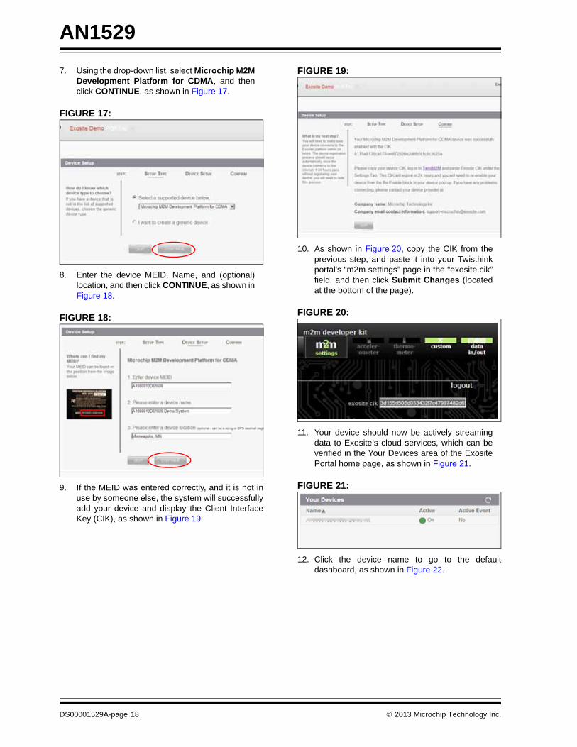
7. Using the drop-down list, select Microchip M2MDevelopment Platform for CDMA, and thenclick CONTINUE, as shown in Figure 17.
FIGURE 17:
8. Enter the device MEID, Name, and (optional)location, and then click CONTINUE, as shown inFigure 18.
FIGURE 18:
9. If the MEID was entered correctly, and it is not inuse by someone else, the system will successfullyadd your device and display the Client InterfaceKey (CIK), as shown in Figure 19.
FIGURE 19:
10. As shown in Figure 20, copy the CIK from theprevious step, and paste it into your Twisthinkportal’s “m2m settings” page in the “exosite cik”field, and then click Submit Changes (locatedat the bottom of the page).
FIGURE 20:
11. Your device should now be actively streamingdata to Exosite’s cloud services, which can beverified in the Your Devices area of the ExositePortal home page, as shown in Figure 21.
FIGURE 21:
12. Click the device name to go to the defaultdashboard, as shown in Figure 22.
DS00001529A-page 18 2013 Microchip Technology Inc.

AN1529
FIGURE 22:
2013 Microchip Technology Inc. DS00001529A-page 19

AN1529
Interacting With the System
The default dashboard for the device has a number oflink icons at the top of the page that will allow you to fur-ther customize the system to represent the device andits data in a way that makes sense for your application.Each of these icons, when clicked, will direct you to addnew features to your Portal.
TABLE 6:
ICON Description
This icon starts the New Dashboard wizard, which allows you to create your own custom dashboard using an array of off-the shelf, or custom-coded, visual widgets.
This icon starts the New Event wizard, where you can set up triggers on incoming data. After the event triggers are set up, you can add e-mail and SMS text alerts when the trigger is activated.
This icon starts the New Script wizard, which allows you to write Lua scripts that process data and device information real-time. Refer to www.lua.org for more information.
This icon directs you to the Portal’s Administration page where you can invite other users to view and/or manage your Portal.
This icon directs you to the Support page of the site where “how-to” videos can be watched, which provide detailed information on each of the options.
DS00001529A-page 20 2013 Microchip Technology Inc.

AN1529
Manage Menu
All pages of your Portal area will show a MANAGEmenu on the left side of the page (see Figure 23). Thismenu directs you to pages that allow you to view, edit,and add to the features of your Portal.
FIGURE 23:
DATA PAGE
The MANAGE > Data page (see Figure 24) shows a listof all data that is flowing into your Portal, or being cre-ated by the real-time processing, or being used to senddata back to your device. You can click on any of thedata elements shown to launch a pop-up window thatdisplays details about the data element. The “+AddData” link at the top right, allows you to add new dataelements to your device’s profile.
FIGURE 24:
2013 Microchip Technology Inc. DS00001529A-page 21

AN1529
DEVICES PAGE
The MANAGE > Devices page (see Figure 25) showsa list of all devices that are interacting with your Portal.You can click any of the devices shown to launch a pop-up window that displays details about your device. The“+Add Device” link at the top right, allows you to addnew devices to your Portal.
FIGURE 25:
The Device pop-up window (see Figure 26) also showsthe Client Identifier Key to your device. This key can beused in API calls, and on the Twisthink M2M Portal, toidentify your device and to remotely interact with yourdevice’s data or meta information.
FIGURE 26:
DS00001529A-page 22 2013 Microchip Technology Inc.

AN1529
SCRIPTS PAGE
The MANAGE > Scripts page (see Figure 27) shows alist of all scripts that are running in your Portal or underyour devices. You can click any of the scripts shown tolaunch a pop-up window that allows you to edit yourscripts. In this window, you will see a number of scriptsare already added to your device.
The scripts shown are performing processing onincoming data to normalize the data making it easy tointeract with them. The “+Add Script” link at the topright, allows you to add new scripts to your devices orto your Portal.
FIGURE 27:
2013 Microchip Technology Inc. DS00001529A-page 23

AN1529
EVENTS AND ALERTS PAGE
The MANAGE > Events page shows a list of all eventsand alerts that are running in your Portal or under yourdevices. You can click any of the events or alerts shownto launch a pop-up window that allows you to edit them.The “+Add Event” and “+Add Alert” links allow you toadd new events and alerts to your devices or to yourPortal.
Events work a lot like oscilloscope triggers – you mustset up the events to trigger on incoming data when thedata goes “out of bounds”. Once an event is set up, youcan create a new alert that is dispatched when theevent is triggered.
Alerts can be either SMS or e-mail alerts, and can beset up to be transmitted one time upon trigger, orrepeating until the event is no longer triggered.
Note that everything that events and alerts can do, canalso be accomplished using scripts. Scripts can goeven further with the complexity of the algorithms andvariety of dispatch capabilities. For example, scriptscan do string parsing and can dispatch to social media,such as Twitter, or an HTTP POST target.
FIGURE 28:
DS00001529A-page 24 2013 Microchip Technology Inc.

AN1529
DASHBOARDS PAGE
The MANAGE > Dashboards page (see Figure 29)shows a list of all dashboards that are in your Portal.You can click the CONFIGURE button on any of thedashboards shown to launch a pop-up window thatallows you to manage the dashboard.
If you click the dashboard line itself, you will beredirected to the dashboard where you can edit yourcustom dashboards using the WSYWIG on-screen edi-tor.
The “+Add Dashboard” link at the top right allows youto add new dashboards to your Portal.
FIGURE 29:
2013 Microchip Technology Inc. DS00001529A-page 25

AN1529
ADMIN PAGE
The MANAGE > Admin page (see Figure 30) allowsyou to administer Portal permissions, resources, anddetails. You can invite other users to view and manageyour portal, check resource allotments and usages foryour Portal, and change details, such as name anddefault dashboard.
FIGURE 30:
Going Further
To further explore the system, please sign up and log into begin. The support page (or the external supportsite) has guides and videos on how to interact with thedetails of the system.
If you want to create your own Portal system for yourbusiness or project, you can sign up at: https://white-box.exosite.com to create a re-branded interface thatis fully customizable for your needs.
DS00001529A-page 26 2013 Microchip Technology Inc.

AN1529
BUILDING THE PROJECT
The M2M platform comes preprogrammed with anexample project that can be used “as is”. Users maywant to build the demonstration project to gain knowl-edge for use when customizing the demonstration soft-ware. For example, although the M2M platform comeswith Ethernet hardware, the demonstration code doesnot supply an Ethernet stack. Users may want to buildtheir own stack or add Microchip’s TCP/IP Stack. Thefollowing description tells how to build the project usingthe MPLAB® X Integrated Development Environment(IDE). Refer to Appendix B: “Referenced Sources”for information on how to obtain MPLAB X IDE.
To build an application, ensure that your project canfind the Verizon DCF library, DCF_Framework.a,which contains the functions that interact with the cellradio and Verizon servers.
Connecting the MPLAB REAL ICE In-Circuit Emulator
The M2M platform has a RJ-11 receptacle that is usedfor downloading binary images and for debugging. TheM2M platform is designed to be used with the MPLABREAL ICE in-circuit emulator.
1. To connect the MPLAB REAL ICE in-circuitemulator to the M2M platform, remove the M2Mtop cover to expose the RJ-11 receptaclemounted inside.
2. Attach the MPLAB REAL ICE in-circuit emulatorRJ-11 cable into the RJ-11 connector of theM2M platform.
3. Attach one end of a USB cable to your MPLABREAL ICE in-circuit emulator and the other endto your PC.
Opening the Project
MPLAB X IDE is Microchip’s Integrated DevelopmentEnvironment (IDE) used to develop, program anddebug your M2M platform software.
1. Connect an external 12V 0.5 Amp power supplyinto the M2M barrel adapter to power the M2Mplatform.
2. Start the MPLAB X IDE and select File > OpenProject.
3. Navigate to the directory that contains the M2Mproject, as shown in Figure 31.
4. Select the project and click Open Project.MPLAB X IDE will begin loading and parsing theproject.
FIGURE 31: OPEN PROJECT DIALOG
2013 Microchip Technology Inc. DS00001529A-page 27
AN1529
Making the Project and Programming the Device
1. The MPLAB X IDE main window title bar shouldcontain the name of the M2M project.
2. Be sure that the M2M project is the activeproject by right clicking on its name within theproject window pane
3. Select Set as Main Project in the resultingpop-up menu.
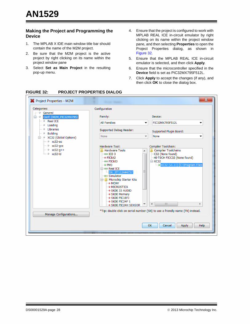
4. Ensure that the project is configured to work withMPLAB REAL ICE in-circuit emulator by rightclicking on its name within the project windowpane, and then selecting Properties to open theProject Properties dialog, as shown inFigure 32.
5. Ensure that the MPLAB REAL ICE in-circuitemulator is selected, and then click Apply.
6. Ensure that the microcontroller specified in theDevice field is set as PIC32MX795F512L.
7. Click Apply to accept the changes (if any), andthen click OK to close the dialog box.
FIGURE 32: PROJECT PROPERTIES DIALOG
DS00001529A-page 28 2013 Microchip Technology Inc.

AN1529
8. As shown in Figure 33, expand the Make andProgram Device icon ( ) to open the menu,and then select Make and Program DeviceMain Project to rebuild the outdated file,program the microcontroller, and start a debugsession.
FIGURE 33: MPLAB® X IDE DIALOG
If programming was successful, a message appearsindicating the microcontroller has been programmedand is now running, as shown in Figure 34.
FIGURE 34: VERIFICATION MESSAGE
2013 Microchip Technology Inc. DS00001529A-page 29

AN1529
TEST MODE
When pressing SW2 during program initialization, theplatform will enter Test mode.
To interact with the platform in Test mode, you mustconnect the RS-232 port to a host computer running aconsole program. Pressing SW2 at power-up will forcethe M2M platform to enter Test mode. A menu ofoptions will be sent to the console port. Press the ESCkey to abort a test. During testing, many platform fea-tures will not be available and no service from the M2Mplatform should be expected until the selected test itemhas completed. Some commands may force a softreset. The menu is as follows:
Twisthink M2M Testing... Select Test Mode:
(1) Sensors Test
(2) 802.15.4 Radio Testing
(3) Cell pass-through mode (802.15 radio off)
(4) Erase Flash
(5) EEPROM Test
(6) GPS Test
(7) USB Test
(8) A/D Test
(ESC) Exit - Soft Reset
Press escape in any mode to return to main menu.
Enter your test number selection.
Sensor Test - Tests the light sensor, accelerometer andtemperature sensors and indicates a PASS or FAILresult for each.
802.15.4 Radio Test – Opens an interactive menu thatallows an operator to place the radio into one of fourmodes:
• Radio CW mode
• Receive mode
• Modulated Packet mode
• Receive Packet mode (an LED blinks when a packet is received)
This test also allows an operator to set the radio outputpower and select which antenna to use (i.e., slotantenna or coax). A PASS or FAIL result is sent to theterminal window.
Cell Pass-through Mode – Turns on the cell moduleand sends it AT commands until the operator pressesthe ESC key.
Erase Flash – This is not an actual test step, but simplya command to erase data from the SPI Flash memorydevice. This task should always succeed.
EEPROM Test – Performs write and read tests of theEEPROM IC. A PASS or FAIL result is sent to theterminal window.
GPS Test – Resets the GPS unit and forces it into acold acquisition mode, which takes about two minutesto complete. New GPS data should be seen on the TextConsole page of the M2M web site.
USB Test – Connect a USB cable and check for a driveto show up. Press ESC when finished.
A/D Test – Outputs the analog-to-digital value seen oneach EXT_AN input. The inputs should be between 0Vand 3.3V.
DS00001529A-page 30 2013 Microchip Technology Inc.

AN1529
APPENDIX A: SOURCE CODE
All of the software covered in this application note isavailable as a single WinZip archive file. This archivecan be downloaded from the Microchip corporate website at:
www.microchip.com
Note: Due to licensing restrictions, the VerizonDevice Control Framework (DCF) isdelivered as a single binary library.Documentation for the DCF API isavailable on the Microchip M2M web pageat: www.microchip.com/m2m.
2013 Microchip Technology Inc. DS00001529A-page 31

AN1529
APPENDIX B: REFERENCED SOURCES
This appendix provides information on the list ofresources that are referenced in this application note.
MICROCHIP TECHNOLOGY INC. RESOURCES
Unless otherwise stated, all resources listed areavailable from the Microchip web site:
www.microchip.com
PIC32 Family Reference Manual Sections
Family Reference Manual sections are available, whichexplain the operation of the PIC32 microcontroller fam-ily architecture and peripheral modules. The specificsof each device family are discussed in the individualfamily’s device data sheet.
PIC32MX795F512L Microcontroller
This 80 MHz, 1.56 DMIPS/MHz microcontrollerfeatures the 32-bit MIPS M4K® Core. Visit this webpage for more information on the features andperipherals included in this device:www.microchip.com/wwwproducts/Devices.aspx?dDocName=en545660.
M2M
Consult this web page for information on Microchip’sM2M offerings: www.microchip.com/m2m.
MCP9800 Temperature Sensor
The MCP9800 is a digital temperature sensor capableof reading temperatures from -55°C to +125°C. Tem-perature data is measured from an integrated tempera-ture sensor and converted to digital word with a userselectable 9-bit to 12-bit Sigma Delta analog-to-digitalconverter.
MPLAB X Integrated Development Environment (IDE)
MPLAB X IDE is a software program that runs on a PC(Windows®, Mac OS®, Linux®) to develop applicationsfor Microchip microcontrollers and digital signal control-lers. It is called an Integrated Development Environ-ment (IDE), because it provides a single integrated“environment” to develop code for embedded micro-controllers. Visit this web page for more information:www.microchip.com/mplabx.
MPLAB REAL ICE™ In-Circuit Emulator
MPLAB REAL ICE™ In-Circuit Emulator System isMicrochip’s next generation high speed emulator forMicrochip Flash DSC and MCU devices. It debugsand programs PIC® MCUs and Flash dsPIC® DSCwith the easy-to-use but powerful graphical userinterface of the MPLAB IDE, included with each plat-form. Visit the following web page for more informa-tion: www.microchip.com/realice.
MPLAB ICD 3
MPLAB ICD 3 In-Circuit Debugger System is Micro-chip's most cost effective high-speed hardware debug-ger/programmer for Microchip Flash DSC and MCUdevices. It debugs and programs Flash PIC microcon-trollers and dsPIC DSCs with the powerful, yet easy-to-use graphical user interface of the MPLAB IDE. Visitthe following web page for more information:www.microchip.com/icd3.
MRF24J40 IEEE 802.15.4 2.4 GHz radio
MRF24J40 is a complete IEEE 802.15.4 radio andoperates in the 2.4GHz freq band. The MRF24J40 sup-ports ZigBee, MiWi™ protocols and proprietary proto-cols to provide an ideal solution for wireless sensornetworks, home automation, building automation andconsumer applications.
Serial Flash (SST25VF080B)
The SST25VF080B devices are enhanced withimproved operating frequency for lower power con-sumption. SST25VF080B SPI serial Flash memoriesare manufactured with SST's proprietary, high-perfor-mance CMOS SuperFlash® technology. The split-gatecell design and thick-oxide tunneling injector attain bet-ter reliability and manufacturability compared with alter-nate approaches.
TCP/IP Stack
Microchip offers a free licensed TCP/IP stack optimizedfor the PIC18, PIC24, dsPIC DSC, and PIC32 micro-controller families. The stack is divided into multiplelayers, where each layer accesses services from oneor more layers directly below it. Visit the following webpage for more information: www.microchip.com/tcpip.
AN1204 “Microchip MiWi™ P2P Wireless Protocol”MiWi P2P is a Peer-to-Peer Wireless Networking Pro-tocol operating on 2.4GHz IEEE 802.15.4. This docu-ment details the supported features and how toimplement them. Simple, application-level data struc-tures and programming interfaces also are described.Visit www.microchip.com/TechDocByProduct.aspx, oraccess the document directly through this link.
DS00001529A-page 32 2013 Microchip Technology Inc.

AN1529
OTHER RESOURCES
Accelerometer
The M2M platform includes an accelerometer, which isavailable from Analog Devices (P/N: ADXL345BCCZ-RLTR), which is capable of measuring acceleration inthree axes. For more information, please visit theAnalog Devices web site: www.analog.com.
DP83848 PHY
The DP83848 PHY is available from Texas Instru-ments. For more information, please visit the TexasInstruments web site: www.ti.com.
HS3001 3G-CDMA Modem
The HS3001 3G-CDMA Modem is available fromNovatel Wireless. The PIC32 microcontroller communi-cates to the modem through a serial UART. For moreinformation on this module, please visit the NovatelWireless web site: www.nvtl.com.
Optical Sensor
The M2M platform includes a light-to-voltage opticalsensor, which is available from Taos (P/N: TSL12T).For more information visit the Taos web site:www.taosinc.com.
MAX-6Q-0 GSP GPS Receiver
This GPS receiver is available from u-blox. Formore information, please visit the u-blox web site:www.u-blox.com.
Twisthink M2M Developer Site
From this site, you can register your M2M platform andpurchase your wireless plan. For more information,please visit the Twisthink developer web site:www.twisthinkm2m.com
Exosite One Platform and Portals
Exosite is a technology company focused on connect-ing devices and systems in the cloud. The MicrochipM2M platform is supported on the “One Platform”cloud-based data system. Exosite Portals is the webapplication that allows users to interact graphically withthe platform. For more information, visit the followingweb sites:
• Portal login: http://microchip.exosite.com
• External support site: http://bit.ly/13RjDd1
• Videos: http://bit.ly/15gdiY0
Verizon M2M Developer Program
The M2M platform RF software and hardware are cer-tified under the Verizon Wireless Open DevelopmentCertification specifications, and have been approvedfor use on the Verizon Wireless network. For moreinformation on the Verizon M2M Developer Program,Open Development Initiative, and the Device ClientFramework, please visit the following web sites:
• http://m2mdeveloper.verizon.com/
• http://opennetwork.verizonwireless.com/aboutOpenDev.aspx
• http://m2mdeveloper.verizon.com/learn/devices
2013 Microchip Technology Inc. DS00001529A-page 33

AN
1529
DS
00
00
15
29
A-p
ag
e 3
4
20
13
Micro
chip
Te
chn
olo
gy In
c.
UA
RT
5U
SB
UA
RT
2
Cellular Module
Serial/DB9,RS-485,
or UART out
micro-USB Connector
Task
Driver
Hardware
PIC32
Legend:
Peripheral
APPENDIX C: SOFTWARE DESCRIPTION
FIGURE C-1: SOFTWARE ARCHITECTURE BLOCK DIAGRAM
Radio Task(not implemented)
Mi-Wi
MRF24J40 Driver
TemperatureSensor Task
File System(FATS)
SPI FlashDriver
microSDDriver
USB Task
US
B D
river
DCF Framework Task(Library)
I2C
2
EEPROMDriver
GPS Task
AccelerometerTask
Cell RX
Cell Task
I2C
1
Ethernet Task(not implemented)
Ethernet MAC
SPI3 SPI1 Ethernet Pins
Diagnostics
UART2Driver
DCF“Rules Engine”
ApplicationTask
Accelerometer
Temperature Sensor
GPS Module
EEPROM
EthernetPHY + Connector
microSDCard
1 MB Serial Flash
802.15.4 Radio
DCF API
Cell TX
DCF Task
(Output to
Plug-in
LED Task
GP
IOLEDs 1-3
Analog-to-Digital
Ana
log
In
Light SensorEXT_AN1EXT_AN2 Console) Task

AN1529
APPENDIX D: RF EXPOSURE INFORMATION
This product complies with FCC RF radiation exposurelimits. This equipment should be installed and operatedwith a minimum distance of 20 cm between the radiatorand your body.
This product complies with FCC RF radiation exposurelimits set forth for an uncontrolled environment. Thewireless system must not be co-located or operating inconjunction with any other antenna or transmitter.
FCC ID: ZPV-TT10315
IC: 9772A-TT10315
FCC Part 15.21 Information Regarding Unapproved Changes or Modifications
Changes and/or modifications not approved by theresponsible party could void the user’s authority tooperate the equipment.
FCC Part 15.105 Information to the User
RSS-210 Compliance
This device complies with Industry Canada RSS-210.Operation is subject to the following two conditions: (1)this device may not cause interference, and (2) thisdevice must accept any interference, includinginterference that may cause undesired operation of thedevice.
RSS-210 Conformité
Cet appareil est conforme avec Industrie Canada RSS-210. Son fonctionnement est soumis aux deuxconditions suivantes: (1) cet appareil ne doit pasprovoquer d'interférences, et (2) cet appareil doitaccepter toute interférence, y compris les interférencespouvant provoquer un fonctionnement indésirable del'appareil.
ICES-003 Compliance Statement
This Class B digital apparatus complies with CanadianICES-003.
Déclaration de conformité à la norme NMB-003
Cet appareil de classe B est conforme à la norme NMB-003 du Canada.
Note: This equipment has been tested andfound to comply with the limits for a ClassB digital device, pursuant to part 15 of theFCC Rules. These limits are designed toprovide reasonable protection againstharmful interference in a residentialinstallation. This equipment generates,uses and can radiate radio frequencyenergy and, if not installed and used inaccordance with the instructions, maycause harmful interference to radiocommunications. However, there is noguarantee that interference will not occurin a particular installation. If thisequipment does cause harmfulinterference to radio or televisionreception, which can be determined byturning the equipment off and on, the useris encouraged to try to correct theinterference by one or more of thefollowing measures:
• Reorient or relocate the receiving antenna.
• Increase the separation between the equipment and receiver.
• Connect the equipment into an outlet on a circuit different from that to which the receiver is connected.
• Consult the dealer or an experienced radio/TV technician for help.
2013 Microchip Technology Inc. DS00001529A-page 35

AN
1529
DS
00
00
15
29
A-p
ag
e 3
6
20
13
Micro
chip
Te
chn
olo
gy In
c.
APPENDIX E: BOARD LAYOUT AND SCHEMATICS
FIGURE E-1: M2M DEVELOPMENT BOARD (TOP VIEW)

2
01
3 M
icroch
ip T
ech
no
log
y Inc.
DS
00
00
15
29
A-p
ag
e 3
7
AN
1529
FIG
URE E-2: M2M DEVELOPMENT BOARD (BOTTOM VIEW)
AN
1529
DS
00
00
15
29
A-p
ag
e 3
8
20
13
Micro
chip
Te
chn
olo
gy In
c.
UTPUT = 3.34V
2V
V3.3
VDD
T I T L E:
C U S T O M E R:
SCHEMATIC DIAGRAMTT Proacive
T I T L E:
C U S T O M E R:
SCHEMATIC DIAGRAMTT Proacive
T I T L E:
C U S T O M E R:
SCHEMATIC DIAGRAMTT Proacive
RWREPLACES TTS0034-0201 2/1/13RWREPLACES TTS0034-0201 2/1/13RWREPLACES TTS0034-0201 2/1/13
UNLESS OTHERWISE SPECIFIEDALL RESISTORS ARE .0625 WATT COMPONENTSAND RESISTANCE VALUES ARE +/- 5%
UNLESS OTHERWISE SPECIFIEDALL RESISTORS ARE .0625 WATT COMPONENTSAND RESISTANCE VALUES ARE +/- 5%
UNLESS OTHERWISE SPECIFIEDALL RESISTORS ARE .0625 WATT COMPONENTSAND RESISTANCE VALUES ARE +/- 5%
UNLESS OTHERWISE SPECIFIED:ALL CAPACITORS ARE RATED AT 50 VOLTS.CAPACITOR TOLERANCES ARE AS FOLLOWS:
.5pF - 5.0pF
5.1pF - 9.1pF
10pF - 820pF
1000pF - 1000uF
+/- .5pF
+/- 10%
+/- .25pF
+/- 5%
UNLESS OTHERWISE SPECIFIED:ALL CAPACITORS ARE RATED AT 50 VOLTS.CAPACITOR TOLERANCES ARE AS FOLLOWS:
.5pF - 5.0pF
5.1pF - 9.1pF
10pF - 820pF
1000pF - 1000uF
+/- .5pF
+/- 10%
+/- .25pF
+/- 5%
UNLESS OTHERWISE SPECIFIED:ALL CAPACITORS ARE RATED AT 50 VOLTS.CAPACITOR TOLERANCES ARE AS FOLLOWS:
.5pF - 5.0pF
5.1pF - 9.1pF
10pF - 820pF
1000pF - 1000uF
+/- .5pF
+/- 10%
+/- .25pF
+/- 5%
TP43
L15
600 ohm @ 100MHz+/- 25%2A
TP53
R93130.0k
1%
D11GREENNP
R70
300NP
D9GREEN
TP57
TP10
C9110pF
C9210pF
R78412.0k1%
C9310pF
48
C7447uF
6.3V20%
PCB1TTF0034-03
R60100k
FIGURE E-3: M2M REFERENCE DESIGN (SHEET 1 OF 7)
XFORMERTO WALL
PAC
K
TO
BATT
1MHz SWITCHING
OUTPUT = 4.99V O
OUTPUT = 3.8
test loopsP0WERpage 2
VIN
VCELL_3.8
V_5.0
V3.3
VIN
V3.3 V3.3
VIN
V3.3
VCELL_3.8
V3.3
V_5.0CELL_PWR_EN
PGSTAT1
VIN_DETECT
TP4
TP3
R108576.0k.0625W1%
R900NP
R48
300
TP52
R73130.0k
1%
C7510pF
R5822k.0625W
R71
0
2.0 mm
J12231
R12310k.0625W
L13
6.8uH30%
C82
.1uF
C871uF
25V10%
R533.09k.0625W1%
TP2
R109249.0k
1%.0625W
TP42
R510.15.25W1%
TP69
C67.01uF25V
U16TPS62110
PGND11
VIN(1)2
VIN(2)3
EN4
SYNC5
LBO6
LBI7
VINA8
AGND9
FB10
GND111
GND212
PG13
SW114
SW215
PGND216
GN
D V
IA1
17G
ND
VIA
218
GN
D V
IA3
19G
ND
VIA
420
GN
D V
IA5
21
C65.1uF
16V10%
C118.047uF
25V10%
L14600 ohm @ 100MHz
+/- 25%2A
L103.3uH
20%
R59
300
C80
10uF25V
C73
.1uF
R6810k
.0625W
TP12
R46100k
R800
R77
0
C7710uF25V
C7922uF
10V20%
R91
0
C696.8uF
16V10%
J13
1
2
34
TP1
D8
BAV99
1
23
R6410k.0625W
U13BQ24103
VSS10
ISET29
PG5
SNS15
OUT11
TTC7
VCC6
CELLS13
IN24
TS12
CE16OUT2
20
PGND218
NC19
IN13
ISET18
VTSB11
PGND117
STAT12
GN
D P
AD
121
BAT14
GN
D P
AD
222
GN
D P
AD
323
GN
D P
AD
424
GN
D P
AD
525
GN
D P
AD
626
GN
D P
AD
727
TP36
C811uF
25V10%
C841uF
25V10%
D16SS22
TP71
C7810pF
C8610pF
R72100k
D5GREEN
C8510uF25V
C72.1uF
D7SS22
R946.98k
.0625W1%
C6822uF
10V20%
U11TPS62160
PGND1
VIN2
EN3
FB5
AGND4
VOS6
SW7
PG8
CTR
_PA
D1
9
CTR
_PA
D2
10
TP
C664.7uF
10V10%
R7910k
.0625W
L12
600 ohm @ 100MHz+/- 25%2A
R89
0
TP23
U12AP7165
IN-11
IN-22
POK3
EN4
GN
D5
FB6
OUT-17OUT-28
CTR
_PA
D9
L11
15uH20%
R955.11k
1%.0625W
C71
10uF25V
R4710k.0625W
R74681.0k1%

2
01
3 M
icroch
ip T
ech
no
log
y Inc.
DS
00
00
15
29
A-p
ag
e 3
9
AN
1529
FIG
2/1/13
page 3
SPA
RE
ETHERNET
ANALOG IN
GER
NER
AL I
/OR
S2
32
GER
NER
AL I
/O
CANpage 4
EXT_RX/TXpage 4
IO_PWR
EXT_MOSIEXT_GPIO3/VOUT
EXT_SCK
EXTGPIO1EXTGPIO2EXTGPIO3EXTGPIO4EXT_CTSEXT_RTS
EXT_AN1
EXT_AN2
CANL
CANH
EXT_MISO
EXT_TX/485AEXT_RX/485B
V3.3
V3.3 V3.3
CANH
CANL
EXT_RX/485B
EXT_TX/485AECOL
ECRS
ERXDV
D O C U M E N T N U M B E R
D A T E:
D O C. R E V.
S C A L E: PAGE: O FNONE 7
012
03-TTS0034-03D O C U M E N T N U M B E R
D A T E:
D O C. R E V.
S C A L E: PAGE: O FNONE 7
012
03-TTS0034-03D O C U M E N T N U M B E R
D A T E:
D O C. R E V.
S C A L E: PAGE: O FNONE 7
012
03-TTS0034-03
U24BMCP6232
6
57
11
23
34
46
5
TP65
R1360
R960NP
TB2123456
7
8
910
R137
0R1381181%
L16
51uHNP
2
3
1
4
U24ACP6232
2
31
84
46
2
TP66
TB1123
45
678
910
TP72
R5662.0625W
NP
D21ESD7C3.3DT5G
TP61
TP64
TP60
TP25
TP38D19
LXES
2SBB
B4-0
26 CH11
CH23
CH34
CH46
VCC5
GN
D2
TP67
TP68
TP74
TP70
R6162.0625W
NP
TP73TP63
C70.1uF
16V10% NP
111uF
6V%
NP
C8910uF
35V10%
R1351181%
TP62
URE E-4: M2M REFERENCE DESIGN (SHEET 2 OF 7)
CELL
ICSP PROGRAMMINGCONNECTOR
DIP SWITCHES FORDEVELOPMENT ONLY.USE RESISTORS INPRODUCTION.
page 6
page 3ETHERNET
DIGITAL I/O
PROTECTION
P0WERpage 1
LIGHT SNSR
page 5
FLASH
RADIO/SPI3
I2C2
SPI1
USB
EX
TER
NA
L
VOUT
RESET
DEBUG
GPSpage 7
CAN
U2/RS485
ACCEL
TEMP/SD
page 4
pages 4,7
page 4
page 4
page 4
page 4
LIGHT_SENSOR
EXT_RTSEXT_CTS
12V_OUT_EN
AN1AN2
PGDPGCMCLR
V3.3
V3.3
V3.3
V3.3
V3.3
V3.3
V3.3 V3.3V_5.0
V3.3
VIN
V3.3
V3.3 V3.3 V3.3 V3.3
V3.3
V3.3 V3.3
V3.3
V_5.0V3.3
ERXCLKERXD0ERXD1ERXD2ERXD3
ERXERR
EMDCEMDIO
ETXENETXD0ETXD1ETXD2ETXD3
VIN_DETECT
ETH_ACTIVITY
I2C2_SDAI2C2_SCL
I2C1_SCLI2C1_SDA
SPI1_SCK
SPI1_MOSIFLASH_CS
RADIO_CS
RADIO_WAKE
RADIO_RESET
SD_CS
ACCEL_INT2ACCEL_INT1
ETH_RESET
CELL_RESET
CELL_RTS
GPS_RESETn
CELL_PWR_EN
SPI3_SCKSPI3_MOSI
U2_ucTX
U2_ucRTS/485_DE_REn
U2_ucRX
U2_ucCTS
SPI1_MISO
SPI3_MISO
STAT1PG
CELL_32kHz
TEMP_ALERT
RADIO_INT
GPS_DATA_READYGPS_INT
CELL_ON-OFF
CELL_CTSCELL_RXCELL_TX
ETXCLK
C88.1uF
16V10%
Q3BMBT3946
4 35
TP13
C58.1uF
16V10%
R141
4.70k1%
R65300
.0625W
TP19
TP56
D18
LXES
2SBB
B4-0
26 CH
CH
CH
CH
VCC
GN
D2
R14222k
R503k.0625W
C531000pF
TP9
R12010k.0625W
U18TSL12T
NC1
GND2
VDD3
OUT4
U10MCP121-315
VDD2
VS
S3
RST1
R114.7k.0625W
Q4AMBT39461
62
C43.1uF
16V10%
R66300
.0625W
SW3
123
46 5
TP76
C94.1uF
16V10%
C63.1uF
16V10%
C110.1uF
16V10%
NP
D1
NZL
6V8A
XV3T
1G
6.8V
R980
NP
R154.7k.0625W
M
Q3AMBT39
1
6D13
YEL
R67 300
C461000pF
TP37D6MBR0520LT1G J9
123456
7
U8
PIC
32M
X795
F512
L
AC2TX/RC27
VSS115
VDD337
RF0/ETXD187
VDD562
RB9/AN933
RA017
U4TX/U1RTS/RD1548
RA561
RD7/ETXCLK84
RE298
RG1397
RE4100
RG1/ETXERR89
RG090
RD4/CN13/OC581
CN14/RD582
VDD686
VCAP85
RF1/ETXD088
RA691
MCLR13
RG9/SS2/ERXCLK14
INT1/RE818
INT2/RE919
CN7/RB520
CN6/RB421
RB3/CN522
U2RX/RF449
U4RX/RD1447
VDD446
PGEC1/RB124 PGED1/RB025
AN6/RB626
U2TX/RF550
RG3/D-56
SDA2/RA359
RA460
RC13/SOSCI73
RC14/CN074
U5RX/RF1240
VUSB55
RB14/ERSD243
VBUS54
RB1034
AVSS31
RB15/ERSD344
VSS345
U5TX/RF1339
AVDD30
RD13/ETXD380
VSS575
AC2RX/RC38
RE194
RE093
VSS236
RA1029
U1TX/RF853
RB727
RA928
RA138
RB13/ERSD142 RB12/ERXD041
AN2/CN4/RB223
RB11/ERXERR35
RC1263
RC1564
VSS465
SCL1/RA1466
SDA1/RA1567
RF351
SS1/RD969
SCK1/RD1070
RD11/EMDC71
SDO1/RD072
RG151
78RD3/OC4
RD12/ETXD279
RD176 RD277
SCL2/RA258
RG2/D+57
RA792
RG1495
VDD12
VDD216
RB8/AN832
U1RX/RF252
RD8/EMDIO68
RD6/ETXEN83
RG1296
RE399
SDI1/RC49
RG7/SDI2/ECRS11RG6/SCK210
RC16
RG8/SDO212
RE53
RE64
RE75
C64.1uF
16V10%
TP55
C611000pF
Q4B
MBT39464 3
5
D3
VESD
05A1
B-H
D1
6.8V
C551000pF
R44
1k.0625W
4
3
2
1
SW1
D20 LXES2SBBB4-026
CH
11
CH
23
CH
34
CH
46
VC
C5
GND2
TP28
U17ST2149
I/O VL21
OE2
I/O VL33
I/O VL44
NC(1)5
VL(2)6
VCC(1)7
NC(2)8
I/O VCC49I/O VCC310
GND11
I/O VCC212I/O VCC113
VCC(2)14
VL(1)15
I/O VL116
TP51
Y420.00 MHz
TP29R1404.7k
R9210k
C621000pF
4
3
2
1
SW2
R139
15
R4100
MOUN
TMO
UNT J3
MIC
RO
USB
12345
67
8
9
10
11
C52.1uF
16V10%
C571000pF
R134.7k.0625W SW4
123
456
R104
0 NP
R101
0 NP
TP35
C3910pF
D14RED
R880 NP
R970
R870 NP
R1050 NP
R1060 NP
C56.1uF
16V10%
C4010pF
C441000pF
U21TJA1042T/3 NP
TXD1
GND2
VCC3
RXD4
STB8
CANH7
CANL6
VIO5
R124.7k.0625W
R62 300
C.1
110
TP21TP17
TP58
R820 NP
R860 NP
C47.1uF
16V10%
RED
GRN
D15RED/GRN
D17BZX84-C1515V
TP39
C514.7uF
6.3V10%
C9010pF

AN
1529
DS
00
00
15
29
A-p
ag
e 4
0
20
13
Micro
chip
Te
chn
olo
gy In
c.
ACTIVITY
RD-
LINK
RD+
TD-
TD+
V3.3
V3.3
TP26
J7
9
10
3
4
5
6
7
8
1
2
11
12
13 14 15 16
R10360.0625W
R23360
.0625W
TP16
FIGURE E-5: M2M REFERENCE DESIGN (SHEET 3 OF 7)
ETHERNET
ETHERNETpage 2
V3.3
V3.3
V3.3
V3.3
V3.3
EMDIO
ERXCLKERXDV
ERXERR
ECRSECOL
ERXD0ERXD1ERXD2ERXD3
ETH_RESET
ETH_ACTIVITY
EMDC
ETXENETXD0ETXD1ETXD2ETXD3
ETXCLK
C4910uF
10V20%
R39 33
R12451
C50.1uF
16V10%
C100.1uF
16V10%
TP33
R12551
R30 47
TP22
TP20
R12651
R1224.87k
1%.0625W
R242.2k
NP
TP31
C48.1uF
16V10%
R43 33C101.1uF
16V10%
R282.2kNP Y5
25.00 MHz
C956.0pF
R12751
C54.1uF
16V10%
C966.0pF
C45.1uF
16V10%
R20 47
C98.1uF
16V10%
R26 47
R27 47
R32 47
TP24
R35 47
R22 47
C9910uF
10V20%
R25 47
R37 47
R121
150.0625W
DP8
3848
M
U9
RXD_0/PHYAD136
TXD_15
25MHz_OUT21
LED_LINK/ANO22
TD+15
TD-14
AGND113
RD+12
RD-11
COL/PHYAD035
PFBIN116
AGND217
AVDD3318
PFBOUT19
RBIAS20
MDIO24
RESET_N23
TX_EN3 TX_CLK2
TXD_37 TXD_26
RESERVED_310
RESERVED_29
RESERVED_18
IO_VDD1
TXD_04
RX_DV/MII_MODE32 RX_CLK31
RX_ER/MDIX_EN34
CRS/CRS_DV/LED_CFG33
PFBIN230
DGND29
X128
X227
IOVDD3326
MDC25
RXD_1/PHYAD237
RXD_2/PHYAD338
RXD_3/PHYAD439
IOGND40
CTR_PAD41
R42 33
TP27
R212.2k
NP
C97.1uF
16V10%
R191.5k
R18 47
R40 33
R38 33

2
01
3 M
icroch
ip T
ech
no
log
y Inc.
DS
00
00
15
29
A-p
ag
e 4
1
AN
1529
FIG
CARD SLOT
MICRO-SD
(INTERNAL)
12345
6789
FRONT VIEW
CANpage 2
U
EXT_RX/TXpage 2
TX
RTS
CTS
RX
MOUNT
V3.3
CANL
CANH
EXT_TX/485A
EXT_RX/485B
0103-TTS0034-03 0103-TTS0034-03 0103-TTS0034-03
J11
5
9
4
8
3
7
2
6
1
1011
TP75
59
J15
MICRO-SD1
2
3
4
5
6
78
9 101112
50
URE E-6: M2M REFERENCE DESIGN (SHEET 4 OF 7)
ACCELEROMETER
TEMP SENSOREEPROM
I2C2page 2
SPI1page 2
FLASHpage 2
TEMP/SDpage 2
FLASH (8Mbit)
ACCELpage 2
DIP SWITCHES FORDEVELOPMENT ONLY.USE RESISTORS INPRODUCTION.
page 22/RS485
DIP SWITCHES FORDEVELOPMENT ONLY.USE RESISTORS INPRODUCTION.
V3.3
V3.3
V3.3
V3.3
V3.3
V3.3
V3.3
V3.3
V3.3 V3.3
TEMP_ALERT
SPI1_MISO
ACCEL_INT2ACCEL_INT1
I2C1_SDAI2C1_SCL
I2C2_SDA
I2C2_SCL
SPI1_SCK
SD_CS
SPI1_MOSI
FLASH_CS
U2_ucTX
U2_ucRTS/485_DE_REn
U2_ucCTS
U2_ucRX
R52
0
U624LC01BT
VCC4
WP5
SCL1
VSS2
SDA3
C117.1uF
16V10%
R1020 NP
U15SST25VF080B
SCK6
CE#1
WP#3
SO2 SI5
HOLD#7
VSS4
VDD8
C115.1uF
16V10%
C341uF
10V10%
R75
0
R810 NP
R143
0
C76.1uF
16V10%
R9910k.0625W
R63
0NP
R830 NP
R2910k.0625WNP
R1030 NP
R134
0
C35.1uF
16V10%
R57
0NP
C38.1uF
16V10%
C114.1uF
16V10%
D10
MMBZ33VAL
NP
TP
U7ADXL345
SDA/SDI/SDIO13 SCL/SCLK14
INT18
VS6
SDO/ALT ADD12
VDD I/O1
GN
D1
2
RSVD13 RSVD2
11
NC10
INT29
CS7
GN
D3
5
GN
D2
4
SW5
123
456
U23MAX3232
C1+1
C1-3
C2+4
C2-5
DIN111
ROUT112
RIN113
DOUT114
V+2
V-6
VCC16
DIN210
DOUT27
ROUT29
RIN28
GN
D15
C112.1uF
16V10%
SW6
1 23
4 56
R107
0 NP
R7610k.0625W
R840 NP
C37.1uF
16V10%
C83.1uF
16V10%
C116.1uF
16V10%
R850 NP
R69
0
C113.1uF
16V10%
U22SN65176
R1
RE2
DE3
D4 VCC
8
B7
A6
GN
D5
R100
0 NP
R13310k.0625W
R132
0NP
TP
U14MCP9800
GND2
ALERT3
VDD1
SCLK4
SDA5

AN
1529
DS
00
00
15
29
A-p
ag
e 4
2
20
13
Micro
chip
Te
chn
olo
gy In
c.
U.FL TO SMA CABLE ASSEMBLY
SLO
T A
NTE
NN
A
GR
OU
ND
ED
SH
IELD
003 TTS0034 03 003 TTS0034 03 003 TTS0034 03
R16
0.0625W
E2EMI SHIELDNP
55
11
44
22
33
66
77
88 9
9
C33
100pF
J4
WIRE HOLE
W2NP
R11951.0625W
R144991%
J5COAX
TP18
IDI
1004
45
L72.2nH5%
NP
FIGURE 35: M2M REFERENCE DESIGN (SHEET 5 OF 7)
ANT_SEL: 0 = SLOT ANT, 1 = ANT2
RADIO
RADIO/SPI3page 2
GR
OU
ND
ED
SH
IELD
GR
OU
ND
ED
SH
IELD
VDD
VDD
VDD
VDD
VDD
VDD
VDD
VDD
VDD
VDD
VDD
VDD
VDD VDD
VDD
VDD
V3.3
SPI3_MISO
RADIO_INTRADIO_RESET
RADIO_CS
SPI3_SCK
SPI3_MOSI
RADIO_WAKE
MR
F24J
40T
U2
GN
D6
36
VDD35
VDD421
GN
D3
22
WAKE15
GN
D2
14RESET
13
GPIO312
GPIO211
VDD735
INT16
SDO17
SDI18
SCK19
CS20
GN
D4
24
NC123
RFN3
RFP2
GPIO07
GN
D1
6
GPIO410
GPIO59
GPIO18
VDD11
VDD24
VDD632
VDD531
OSC134
OSC233
NC430NC329
LPOSC128
LPOSC227
NC226
GN
D5
25
VDD837
NC538
VDD939
LCAP40
GND_VIA141 GND_VIA242 GND_VIA343 GND_VIA444 GND_VIA545 GND_VIA646 GND_VIA747 GND_VIA848 GND_VIA949
C2947pF
L1
5.6nH5%
C7.01uF25V
R11.2k
C22
20pF
C26.01uF
25V
C547pF
R64991%
R11210k
U3NC7SZ125
Y4
A2
OE1
GND3
VCC5
L310nH5%
C16.01uF
25V
C92.2uF
6.3V20%
C247pF
R22.2k
.0625W
C11100pF
C1.5pF
R116
0
C20.1uF
16V10%
R110
0
L210nH5%
C1910pF R118
51.0625W
TP5
R551NP
R11110k
R11310k
TP7
R310k.0625W
TP14IDI 100445
Y120.00 MHz
R11410kNP
C1212pF
R115
0
R117
0
C23
20pF
Y22450BP39C100A
GN
D1
1
IN4
OUT2
GN
D2
3
C8.01uF25V
C1812pF
C27.01uF
25V
C141uF
10V10%
C3.1uF
16V10%
U1
SE24
31L-
R
B21
B12
DNC13
DNC24
VDD5
TR6
DNC37
DNC48
GND19
GND210
GND311
GND412
ANT213
GND514
ANT115
ANT_SEL16
DNC517
GND618
VCC219
CSD20
CPS21
VCC122
BOUT23
CTX24
GND_PAD125
GND_PAD226
GND_PAD327
GND_PAD428
GND_PAD529
GND_PAD630
GND_PAD731
GND_PAD832
GND_PAD933
GND_PAD1034
GND_PAD1135
GND_PAD1236
GND_PAD1337
GND_PAD1438
GND_PAD1539
TP6
C1010pF
C1747pF
C2547pF
Y32450BP39C100A
GN
D1
1
IN4
OUT2
GN
D2
3
C4
.5pF

2
01
3 M
icroch
ip T
ech
no
log
y Inc.
DS
00
00
15
29
A-p
ag
e 4
3
AN
1529
FIG
TOBA
ONBOARDCHIPANTENNA
D O C U M E N T N U M B E R D O C R E
0103-TTS0034-03D O C U M E N T N U M B E R D O C R E
0103-TTS0034-03D O C U M E N T N U M B E R D O C R E
0103-TTS0034-03
R12851.0625W
E3ANTENNA
12
C593.3pF
TP34IDI 100445
J10
OAX
R45
0.0625W
L810nH
5%
R414991%
L96.8nH
5%C6010pFNP
URE 36: M2M REFERENCE DESIGN (SHEET 6 OF 7)
INTE
RN
AL
CELL INTERFACEU.FL TO SMA CABLE ASSEMBLYO:FFOARDNTENNA
page 2CELL
GPIO_6
CELL_USB-
CELL_USB+
PHON
PSLOGIC
ADCIN1
ON/OFF
GPIO_4
GPIO_1GPIO_2GPIO_3
UART2_RXUART2_TX
GPIO_5
CLK32K_BUF
CELL_VBUS
VCELL_3.8
VCELL_3.8
V3.3
V1.8
V1.8
VCELL_3.8
CELL_RXCELL_CTS
CELL_RESET
CELL_ON-OFF
CELL_32kHz
CELL_RTS
CELL_TX
Q2MMBT3904
TP32
MOUNTS
J14
1
2
3
4
5
7
11131521
2729
35
37
54
56
58606264
69
74
75
77
85
86
87
88
89
90
91
92
93
94
95
96
97
98
99
100
6870
101102103104
TP41TP40
R17
0
TP49
C1061uF
10V10%
C109.1uF
16V10%
U19MCP1700
OUT2
IN3
GN
D1
TP46
TP30
D4NZL6V8AXV3T1G6.8V
C
TP44TP47
R130
4.7k
+C1031000uF6.3V10%
U20ST2149
I/O VL21
OE2
I/O VL33
I/O VL44
NC
15
VL26VCC1
7
NC
28
I/O VCC49 I/O VCC3
10
GN
D11
I/O VCC212 I/O VCC113
VCC214 VL1
15
I/O VL116
R36
3.6
D12GREEN
C107.01uF
25V
C108.1uF
16V10%
W1
NP
TP45
R33
3.6
R12910k
C104.1uF
16V10%
R544.7k
.0625W
Q1
MMBT3904
R55240
.0625W TP54
C1051uF
10V10%
R49
4.7k
R13110k
.0625WNP
SPRI
NG LO
ADED
TAB
S
MOUN
TING
TAB
S (G
ROUN
DED)
HS
3001 C
ELL M
OD
ULE
GND
GND
ANT
M1HS 3001
1
2
3
4
5
6
7
M O
U N
T S
J8
MICRO USB
1
2
3
4
5
678
+C1021000uF6.3V10%
R31
0

AN
1529
DS
00
00
15
29
A-p
ag
e 4
4
20
13
Micro
chip
Te
chn
olo
gy In
c.
ss than 3/4 inchro stripline. should be stripline V3.3
J1COAX
NP
L4
6.8nH5%
FL11575.42 MHz
INPUT4
GN
D1
2G
ND
23
GN
D3
5
OUTPUT1
C2415pF
U5MAX2674
VCCA1
RFINB1
GNDDCC1
ANTC2
GNDACB2
RFOUTSHDNA2
C133pF
F
C30
100pF
D2ESD0P8RFL
14
23
C61000pF
NP
C151000pF
NP
C2115pF
J2COAX
E1 ANTENNA
FIGURE 37: M2M REFERENCE DESIGN (SHEET 7 OF 7)
GPS traces leshould be micLonger traces
I2C2page 2
GPSpage 2
V3.3
V3.3
V3.3
GPS_RESETn
I2C2_SDA
I2C2_SCL
GPS_INT
GPS_DATA_READY
TP11
R9
0.0625W
J6
(TEST)NP
12345
TP15 C36.01uF
25V
TP8
C3210p
L6
1500 ohm @ 100MHz+/- 25%500mA
NP
C4215pFNP
C4147pFNP
R724k.0625W
C2839pF
R340
.0625W
U4MAX-6Q-0
VRESET9
SDA216
RXD13
GN
D1
1VCC_IO
7
SCL217
RESERVED218
TXD12
GN
D3
12
ANTON13
VCC_RF14
RESERVED115
GN
D2
10
EXTINT05
TIMEPULSE4
V_B
CK
P6
RF_IN11
VCC8
R83.3k
.0625W
C31.1uF
16V10%
L5
1500 ohm @ 100MHz+/- 25%500mA
NP

Note the following details of the code protection feature on Microchip devices:
• Microchip products meet the specification contained in their particular Microchip Data Sheet.
• Microchip believes that its family of products is one of the most secure families of its kind on the market today, when used in the intended manner and under normal conditions.
• There are dishonest and possibly illegal methods used to breach the code protection feature. All of these methods, to our knowledge, require using the Microchip products in a manner outside the operating specifications contained in Microchip’s Data Sheets. Most likely, the person doing so is engaged in theft of intellectual property.
• Microchip is willing to work with the customer who is concerned about the integrity of their code.
• Neither Microchip nor any other semiconductor manufacturer can guarantee the security of their code. Code protection does not mean that we are guaranteeing the product as “unbreakable.”
Code protection is constantly evolving. We at Microchip are committed to continuously improving the code protection features of ourproducts. Attempts to break Microchip’s code protection feature may be a violation of the Digital Millennium Copyright Act. If such actsallow unauthorized access to your software or other copyrighted work, you may have a right to sue for relief under that Act.
Information contained in this publication regarding deviceapplications and the like is provided only for your convenienceand may be superseded by updates. It is your responsibility toensure that your application meets with your specifications.MICROCHIP MAKES NO REPRESENTATIONS ORWARRANTIES OF ANY KIND WHETHER EXPRESS ORIMPLIED, WRITTEN OR ORAL, STATUTORY OROTHERWISE, RELATED TO THE INFORMATION,INCLUDING BUT NOT LIMITED TO ITS CONDITION,QUALITY, PERFORMANCE, MERCHANTABILITY ORFITNESS FOR PURPOSE. Microchip disclaims all liabilityarising from this information and its use. Use of Microchipdevices in life support and/or safety applications is entirely atthe buyer’s risk, and the buyer agrees to defend, indemnify andhold harmless Microchip from any and all damages, claims,suits, or expenses resulting from such use. No licenses areconveyed, implicitly or otherwise, under any Microchipintellectual property rights.
2013 Microchip Technology Inc.
QUALITY MANAGEMENT SYSTEM CERTIFIED BY DNV
== ISO/TS 16949 ==
Trademarks
The Microchip name and logo, the Microchip logo, dsPIC, FlashFlex, KEELOQ, KEELOQ logo, MPLAB, PIC, PICmicro, PICSTART, PIC32 logo, rfPIC, SST, SST Logo, SuperFlash and UNI/O are registered trademarks of Microchip Technology Incorporated in the U.S.A. and other countries.
FilterLab, Hampshire, HI-TECH C, Linear Active Thermistor, MTP, SEEVAL and The Embedded Control Solutions Company are registered trademarks of Microchip Technology Incorporated in the U.S.A.
Silicon Storage Technology is a registered trademark of Microchip Technology Inc. in other countries.
Analog-for-the-Digital Age, Application Maestro, BodyCom, chipKIT, chipKIT logo, CodeGuard, dsPICDEM, dsPICDEM.net, dsPICworks, dsSPEAK, ECAN, ECONOMONITOR, FanSense, HI-TIDE, In-Circuit Serial Programming, ICSP, Mindi, MiWi, MPASM, MPF, MPLAB Certified logo, MPLIB, MPLINK, mTouch, Omniscient Code Generation, PICC, PICC-18, PICDEM, PICDEM.net, PICkit, PICtail, REAL ICE, rfLAB, Select Mode, SQI, Serial Quad I/O, Total Endurance, TSHARC, UniWinDriver, WiperLock, ZENA and Z-Scale are trademarks of Microchip Technology Incorporated in the U.S.A. and other countries.
SQTP is a service mark of Microchip Technology Incorporated in the U.S.A.
GestIC and ULPP are registered trademarks of Microchip Technology Germany II GmbH & Co. KG, a subsidiary of Microchip Technology Inc., in other countries.
All other trademarks mentioned herein are property of their respective companies.
© 2013, Microchip Technology Incorporated, Printed in the U.S.A., All Rights Reserved.
Printed on recycled paper.
ISBN: 9781620773932
Microchip received ISO/TS-16949:2009 certification for its worldwide
DS00001529A-page 45
headquarters, design and wafer fabrication facilities in Chandler and Tempe, Arizona; Gresham, Oregon and design centers in California and India. The Company’s quality system processes and procedures are for its PIC® MCUs and dsPIC® DSCs, KEELOQ® code hopping devices, Serial EEPROMs, microperipherals, nonvolatile memory and analog products. In addition, Microchip’s quality system for the design and manufacture of development systems is ISO 9001:2000 certified.

DS00001529A-page 46 2013 Microchip Technology Inc.
AMERICASCorporate Office2355 West Chandler Blvd.Chandler, AZ 85224-6199Tel: 480-792-7200 Fax: 480-792-7277Technical Support: http://www.microchip.com/supportWeb Address: www.microchip.com
AtlantaDuluth, GA Tel: 678-957-9614 Fax: 678-957-1455
BostonWestborough, MA Tel: 774-760-0087 Fax: 774-760-0088
ChicagoItasca, IL Tel: 630-285-0071 Fax: 630-285-0075
ClevelandIndependence, OH Tel: 216-447-0464 Fax: 216-447-0643
DallasAddison, TX Tel: 972-818-7423 Fax: 972-818-2924
DetroitFarmington Hills, MI Tel: 248-538-2250Fax: 248-538-2260
IndianapolisNoblesville, IN Tel: 317-773-8323Fax: 317-773-5453
Los AngelesMission Viejo, CA Tel: 949-462-9523 Fax: 949-462-9608
Santa ClaraSanta Clara, CA Tel: 408-961-6444Fax: 408-961-6445
TorontoMississauga, Ontario, CanadaTel: 905-673-0699 Fax: 905-673-6509
ASIA/PACIFICAsia Pacific OfficeSuites 3707-14, 37th FloorTower 6, The GatewayHarbour City, KowloonHong KongTel: 852-2401-1200Fax: 852-2401-3431
Australia - SydneyTel: 61-2-9868-6733Fax: 61-2-9868-6755
China - BeijingTel: 86-10-8569-7000 Fax: 86-10-8528-2104
China - ChengduTel: 86-28-8665-5511Fax: 86-28-8665-7889
China - ChongqingTel: 86-23-8980-9588Fax: 86-23-8980-9500
China - HangzhouTel: 86-571-2819-3187 Fax: 86-571-2819-3189
China - Hong Kong SARTel: 852-2943-5100 Fax: 852-2401-3431
China - NanjingTel: 86-25-8473-2460Fax: 86-25-8473-2470
China - QingdaoTel: 86-532-8502-7355Fax: 86-532-8502-7205
China - ShanghaiTel: 86-21-5407-5533 Fax: 86-21-5407-5066
China - ShenyangTel: 86-24-2334-2829Fax: 86-24-2334-2393
China - ShenzhenTel: 86-755-8864-2200 Fax: 86-755-8203-1760
China - WuhanTel: 86-27-5980-5300Fax: 86-27-5980-5118
China - XianTel: 86-29-8833-7252Fax: 86-29-8833-7256
China - XiamenTel: 86-592-2388138 Fax: 86-592-2388130
China - ZhuhaiTel: 86-756-3210040 Fax: 86-756-3210049
ASIA/PACIFICIndia - BangaloreTel: 91-80-3090-4444 Fax: 91-80-3090-4123
India - New DelhiTel: 91-11-4160-8631Fax: 91-11-4160-8632
India - PuneTel: 91-20-2566-1512Fax: 91-20-2566-1513
Japan - OsakaTel: 81-6-6152-7160 Fax: 81-6-6152-9310
Japan - TokyoTel: 81-3-6880- 3770 Fax: 81-3-6880-3771
Korea - DaeguTel: 82-53-744-4301Fax: 82-53-744-4302
Korea - SeoulTel: 82-2-554-7200Fax: 82-2-558-5932 or 82-2-558-5934
Malaysia - Kuala LumpurTel: 60-3-6201-9857Fax: 60-3-6201-9859
Malaysia - PenangTel: 60-4-227-8870Fax: 60-4-227-4068
Philippines - ManilaTel: 63-2-634-9065Fax: 63-2-634-9069
SingaporeTel: 65-6334-8870Fax: 65-6334-8850
Taiwan - Hsin ChuTel: 886-3-5778-366Fax: 886-3-5770-955
Taiwan - KaohsiungTel: 886-7-213-7828Fax: 886-7-330-9305
Taiwan - TaipeiTel: 886-2-2508-8600 Fax: 886-2-2508-0102
Thailand - BangkokTel: 66-2-694-1351Fax: 66-2-694-1350
EUROPEAustria - WelsTel: 43-7242-2244-39Fax: 43-7242-2244-393Denmark - CopenhagenTel: 45-4450-2828 Fax: 45-4485-2829
France - ParisTel: 33-1-69-53-63-20 Fax: 33-1-69-30-90-79
Germany - MunichTel: 49-89-627-144-0 Fax: 49-89-627-144-44
Italy - Milan Tel: 39-0331-742611 Fax: 39-0331-466781
Netherlands - DrunenTel: 31-416-690399 Fax: 31-416-690340
Spain - MadridTel: 34-91-708-08-90Fax: 34-91-708-08-91
UK - WokinghamTel: 44-118-921-5869Fax: 44-118-921-5820
Worldwide Sales and Service
11/29/12