Embed Size (px)
Citation preview
HCTL Open International Journal of Technology Innovations and Research (IJTIR) http://ijtir.hctl.org Volume 17, September 2015 e-ISSN: 2321-1814, ISBN (Print): 978-1-94416-926-8
Salah Gh. Ramadan, Gamal M. Sarhan, Ayman Y. Yousef, Microcontroller Based Space Vector PWM Control of Three Phase Voltage Source Inverter.
Page 1
Microcontroller Based Space Vector PWM Control of Three Phase Voltage Source Inverter Salah Gh. Ramadan1, Gamal M. Sarhan2, Ayman Y. Yousef3 [email protected], [email protected], [email protected] Abstract The objective of this paper is to present a design and implementation of Space Vector Pulse Width Modulation (SVPWM) technique to generate the sequence pattern of the PWM inverter driving signals. The aim of the Space Vector Modulator (SVM) is to optimize the operational characteristics of ac drive by minimizing the harmonics of the currents. The SVM is implemented in the High Speed Output (HSO) unit of the microcontroller which accepts the outputs of the direct and quadrature current controllers and the flux position angle from the machine model, and gives the three switching pulse patterns required to drive the inverter unit. The essential dead time required for the switching devices is implemented to protect the power switches of the same inverter arm against the short circuit current during the switching transients. In this paper, the space vector modulator and the dead time compensator is configured and implemented completely in a single chip Intel 80C196KC microcontroller in order to minimize the hardware of the system. Keywords Space vector PWM, Frame of Reference, VSI, Switching patterns, Microcontroller.
Introduction Space vector pulse width modulation technique has become a major PWM technique for three-phase Voltage Source Inverters (VSI) in control of AC motors and drives applications. Space vector pulse width modulation is a more advanced real-time modulation technique for generating sine wave that gives a higher voltage to drive the motor with lower total harmonic distortion. The space vector method of analysis is originally developed as a vector approach to Pulse Width Modulation (PWM) and it enables representation of the three phase quantities (voltages or currents) by a single complex vector [1].
1,2Electrical Engineering Department, Faculty of Engineering at Benha,Benha University, Benha, Egypt. 3Electrical Engineering Department, Faculty of Engineering at Shoubra, Benha University, Cairo, Egypt.
HCTL Open International Journal of Technology Innovations and Research (IJTIR) http://ijtir.hctl.org Volume 17, September 2015 e-ISSN: 2321-1814, ISBN (Print): 978-1-94416-926-8
Salah Gh. Ramadan, Gamal M. Sarhan, Ayman Y. Yousef, Microcontroller Based Space Vector PWM Control of Three Phase Voltage Source Inverter.
Page 2
This method of analysis has been effectively used in analysis of the three phase machines and also of the three phase inverters. Space vector pulse width modulation is also compatible for use in vector control (Field orientation) of AC motor and drives applications. Generally, It is known that, the variable output voltage of the inverter with a maximum fundamental component, wide linear modulation range, low switching loss, and minimum harmonics are considered as the targets of any modulation technique. Because the space vector pulse width modulation technique is able to achievethese demands, it has become better and is widely used than the conventional modulation technique.
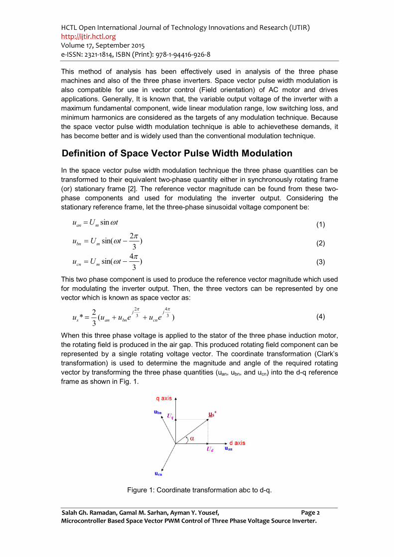
Definition of Space Vector Pulse Width Modulation In the space vector pulse width modulation technique the three phase quantities can be transformed to their equivalent two-phase quantity either in synchronously rotating frame (or) stationary frame [2]. The reference vector magnitude can be found from these two-phase components and used for modulating the inverter output. Considering the stationary reference frame, let the three-phase sinusoidal voltage component be:
(1)
(2)
(3)
This two phase component is used to produce the reference vector magnitude which used for modulating the inverter output. Then, the three vectors can be represented by one vector which is known as space vector as:
(4)
When this three phase voltage is applied to the stator of the three phase induction motor, the rotating field is produced in the air gap. This produced rotating field component can be represented by a single rotating voltage vector. The coordinate transformation (Clark’s transformation) is used to determine the magnitude and angle of the required rotating vector by transforming the three phase quantities (uan, ubn, and ucn) into the d-q reference frame as shown in Fig. 1.
Figure 1: Coordinate transformation abc to d-q.
)3
2sin( tUu mbn
)3
4sin( tUu mcn
tUu man sin
)(32* 3
43
2 j
cn
j
bnans eueuuu

HCTL Open International Journal of Technology Innovations and Research (IJTIR) http://ijtir.hctl.org Volume 17, September 2015 e-ISSN: 2321-1814, ISBN (Print): 978-1-94416-926-8
Salah Gh. Ramadan, Gamal M. Sarhan, Ayman Y. Yousef, Microcontroller Based Space Vector PWM Control of Three Phase Voltage Source Inverter.
Page 3
The relation between these two reference frames of a two dimensional plane and the three phase’s vectors of a three dimensional plane in matrix form is:
(5)
Then, the magnitude of the rotating vector and its angle are:
(6)
(7)
Principle of Space Vector Pulse Width Modulation Space vector pulse width modulation refers to special switching sequence of the upper three devices of three-phase voltage source inverter. This special switching technique for the power device results in three pseudo-sinusoidal currents in the stator phases [3]. Consider the diagram of a three phase voltage source inverter shown in Fig. 2.
Figure 2: Three-Phase VSI Inverter
The inverter output voltage is shaped by the six power switches (S1 to S6). When one of the upper switches (S1, S3, or S5) is switched ON, the corresponding lower switch (S4, S6, or S2) is switched OFF. Therefore, the output voltage is determined by the ON and OFF states of the upper switches (S1, S3, and S5). The relationship between the switching variable vector [a ,b, c]t and the line-to-line output voltage vector [UabUbcUca]t and the phase (line-to-neutral) output voltage vector [uaubuc]t are given by Equ. 8 and Equ.9 respectively.
(8)
cn
bn
an
q
d
uuu
UU
232302
12
11
32
)22*qds UUu
d
q
UU1tan
cba
UUUU
dc
ca
bc
ab
101110
011

HCTL Open International Journal of Technology Innovations and Research (IJTIR) http://ijtir.hctl.org Volume 17, September 2015 e-ISSN: 2321-1814, ISBN (Print): 978-1-94416-926-8
Salah Gh. Ramadan, Gamal M. Sarhan, Ayman Y. Yousef, Microcontroller Based Space Vector PWM Control of Three Phase Voltage Source Inverter.
Page 4
(9)
The operating status of the switches in the 2-level voltage source inverter shown in Fig.2 can be represented by switching states shown in Table 1.
Space Vector Switching State
ON-State Switch Vector Definition
Zero Vector u0 [0 0 0] Q4 Q6 Q2 0
Active Vector
u1 [1 0 0] Q1 Q6 Q2 u1=(2/3)Udcej0
u2 [1 1 0] Q1 Q3 Q2 u1=(2/3)Udcejπ/3
u3 [0 1 0] Q4 Q3 Q2 u1=(2/3)Udcej2π/3 u4 [0 11] Q4 Q3 Q5 u1=(2/3)Udcejπ u5 [0 0 1] Q4 Q6 Q5 u1=(2/3)Udcej4π/3 u6 [1 0 1] Q1 Q6 Q5 u1=(2/3)Udcej5π/3
Zero Vector u7 [1 1 1] Q1 Q3 Q5 0
Table 1: Switching States of SVPWM
The switching state “1” indicate that one of the three upper switches (Q1, Q3, or Q5) in inverter arms is turned ON, in this case the inverter terminal voltage (Uan, Ubn, Ucn) is positive and equal to (Udc) while the switching state “0” indicate that the inverter terminal voltage is equal to zero due to the conduction of one of the three lower switches (Q4, Q6, or Q2). In the two level voltage source inverter shown in Fig.1, there are only eight possible switching states as shown in Table 1. For example, the switching state [100] corresponds to the conduction of Q1, Q6, and Q2 in the inverter arms a, b, and c, respectively with note that, the switching states, [111] and [000] are zero states and the other states are active states. The eight possible switching states which produce eight voltage vectors in case of two level voltage source inverter can be represented in complex plane as shown in Fig. 3.
Figure 3: Space Vector Diagram fora Two-Level Inverter
cba
U
uuu
dc
cn
bn
an
211121112
3

HCTL Open International Journal of Technology Innovations and Research (IJTIR) http://ijtir.hctl.org Volume 17, September 2015 e-ISSN: 2321-1814, ISBN (Print): 978-1-94416-926-8
Salah Gh. Ramadan, Gamal M. Sarhan, Ayman Y. Yousef, Microcontroller Based Space Vector PWM Control of Three Phase Voltage Source Inverter.
Page 5
The six non-zero vectors (u1 to u6) form the axes of a regular hexagon with six equal sectors (each of any two adjacent non-zero vectors separated by angle equal to 60o) and two zero vectors (u0 and u7) lies in the center of the hexagon. The binary notation on the hexagon axes indicates the switch state of the inverter arms. In this case, logic 1 means that the upper switch (Q1, Q3, or Q5) being ON and logic 0 means that the lower switch (Q4, Q6, or Q2) of the arm is ON. The most significant bit in the logic notation is for arm A, the middle bit is related to arm B, and the least significant is for arm C.
Space Vector PWM Time Duration The reference vector locus with respect to time should be a circle instead of hexagon as locus of the vector sum of three voltages gives a circle to produces a sinusoidal output of the inverter using this SVPWM technique. In order to achieve this target vector in each sector is sampled for a specific duration using active and zero vectors and hence we can obtain required vector of corresponding instant [4]. The sampling duration for non-zero and zero vectors to produce the vector at specific instant can be obtained using volt second balance equation. Fig. 4 shows the switching sequence of Space vector modulation output of sector-1.
Figure 4: Switching sequence of SVM output of sector-1
It should be noted that, the generated space vector PWM waveforms are symmetrical with respect to the middle of each PWM period. When the reference voltage and the sample periods are known, the switching time duration (T1, T2, and T0) of sector-1 can be determined with the situation shown in Fig. 5.
Figure 5: Principle of space vector time calculation
HCTL Open International Journal of Technology Innovations and Research (IJTIR) http://ijtir.hctl.org Volume 17, September 2015 e-ISSN: 2321-1814, ISBN (Print): 978-1-94416-926-8
Salah Gh. Ramadan, Gamal M. Sarhan, Ayman Y. Yousef, Microcontroller Based Space Vector PWM Control of Three Phase Voltage Source Inverter.
Page 6
Using the volt-seconds balance principle, thus:
(10)
(11)
(12)
(13)
(14)
(15)
Where:
T1, T2, and T0: Times during at which u1, u2, and zero-vector are applied.
Ts: Switching time (switching cycle), ∆t: Sampling time, fs : Switching frequency.
α : Phase angle of output vector, 0 ≤ α ≤ 60o
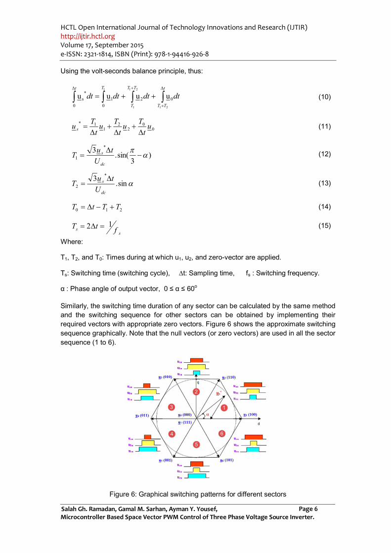
Similarly, the switching time duration of any sector can be calculated by the same method and the switching sequence for other sectors can be obtained by implementing their required vectors with appropriate zero vectors. Figure 6 shows the approximate switching sequence graphically. Note that the null vectors (or zero vectors) are used in all the sector sequence (1 to 6).
Figure 6: Graphical switching patterns for different sectors
210 TTtT
dtdtdtdtt
TT
TT
T
Tt
21
21
1
1
020
10
*s uuuu
00
22
11* u
tTu
tTu
tTu s
)3
sin(.3 *
1
dc
s
UtuT
sin.3 *
2dc
s
UtuT
ss ftT 12

HCTL Open International Journal of Technology Innovations and Research (IJTIR) http://ijtir.hctl.org Volume 17, September 2015 e-ISSN: 2321-1814, ISBN (Print): 978-1-94416-926-8
Salah Gh. Ramadan, Gamal M. Sarhan, Ayman Y. Yousef, Microcontroller Based Space Vector PWM Control of Three Phase Voltage Source Inverter.
Page 7
According to Fig. 6, the switching time at each sector for the upper and lower switches is summarized in Table 2.
Sectors Upper Switches (S1, S3, S5)
Lower Switches (S4, S6, S2)
Sector 1 S1 = t1 + t2 + t0/2, S3 = t2 + t0/2
S5 = t0/2 S4 = t0/2, S6 = t1 + t0/2
S2 = t1 + t2 + t0/2
Sector 2 S1 = t1 + t0/2, S3 = t1 + t2 + t0/2 S5 = t0/2
S4 = t1 + t0/2, S6 = t0/2 S2 = t1 + t2 + t0/2
Sector 3 S1 = t0/2, S3 = t1 + t2 + t0/2 S5 = t2 + t0/2
S4 = t1 + t2 + t0/2, S6 = t0/2 S2 = t1 + t0/2
Sector 4 S1 = t0/2, S3 = t1 + t0/2 S5 = t1 + t2 + t0/2
S4 = t1 + t2 + t0/2, S6 = t2 + t0/2 S2 = t0/2
Sector 5 S1 = t2 + t0/2, S3 = t0/2 S5 = t1 + t2 + t0/2
S4 = t1 + t0/2, S6 = t1 + t2 + t0/2 S2 = t0/2
Sector 6 S1 = t1 + t2 + t0/2, S3 = t0/2 S5 = t1 + t0/2
S4 = t0/2, S6 = t1 + t2 + t0/2 S2 = t2 + t0/2
Table 2: Calculation of Switching Time at each Sector Space Vector Pulse Width Modulation Implementation
The generation of space vector PWM of the inverter side is implemented by using the High Speed Output (HSO) unit of the microcontroller for the lines (HSO.0, HSO.1, and HS0.2) with the aid of some hardware circuits. A logic circuit is used to generate six base signals required for the inverter transistors. The two signals required to drive the two transistors in the same arm must be complement to each other. With this inverter, care must be taken to ensure a few microseconds elapse after turn of the transistor before its complementary transistor is turned on [5]. Otherwise there is risk of reconduction of the outgoing transistor giving a short circuit across the dc source via the two transistors. This small time is called a dead time which is required to protect the switching power devices against short circuit condition. In present work, An inverter logic gates is used to invert the SVM outputs (HSO.0, HSO.1, and HS0.2) obtained from the HSO unit to their complementary and a simple lag circuit (R-C circuit) is used to obtain 20 µsec between the edges of each pulse and its complementary. The actual signals applied to the inverter transistors are shown in Fig. 7 where the dead time is introduced.
Microcontroller HSO Unit Configuration The Content Addressable Memory (CAM) file of the HSO unit, shown in Fig. 8 is the center of control. One CAM register is compared with timer values every state time, taking 8 state times to compare all CAM registers with the timers. This defines the resolution of HSO to be 8 state times (1µsec at an oscillator frequency of 16 MHz). Each CAM register is 24 bits wide. Sixteen bits specify the time at which the action is to be carried out, and 8 bits define the action to take place.The HSO unit can generate two types of interrupts. The HSO execution interrupt can be generated (if enabled) for HSO commands which change one or more of the six output pins. The other HSO interrupt can be generated by any other HSO command, (i.e. triggering the A/D converter, resetting Timer 2).

HCTL Open International Journal of Technology Innovations and Research (IJTIR) http://ijtir.hctl.org Volume 17, September 2015 e-ISSN: 2321-1814, ISBN (Print): 978-1-94416-926-8
Salah Gh. Ramadan, Gamal M. Sarhan, Ayman Y. Yousef, Microcontroller Based Space Vector PWM Control of Three Phase Voltage Source Inverter.
Page 8
Figure 7: Generation of driving pulses including of dead time effect.
Figure 8: HSO unit block diagram.
The HSO unit is programmed to realize the space vector modulator using Timer 1 as the reference timer for the HSO command and incremented every 8 state times. The comparator has a chance to look all 8 CAM registers before Timer 1 changes its value. The lines HSO.0, HSO.1, and HS0.2 are configured using HSO COMMAND register represent the output of the SVM to drive the three phase transistorized inverter. The timing diagram shown in Fig. 9 describes the operation of the SVM.

HCTL Open International Journal of Technology Innovations and Research (IJTIR) http://ijtir.hctl.org Volume 17, September 2015 e-ISSN: 2321-1814, ISBN (Print): 978-1-94416-926-8
Salah Gh. Ramadan, Gamal M. Sarhan, Ayman Y. Yousef, Microcontroller Based Space Vector PWM Control of Three Phase Voltage Source Inverter.
Page 9
Figure 9: Timing Diagram with Interrupt at middle of the Zero Voltage Vector.
Considering that the reference voltage space vector lies in sector-1 as shown in Fig. 3 and referring to Fig. 4, the output of the space vector modulator has the sequence u0 u1 u2 u7 u2 u1 u0. In order to obtain this time adaptation, the HSO_COMMAND is loaded to clear Pin.0, Pin.1, and Pin.2 in times t0/2, (t0/2-t1), and (t0/2-t1-t2) respectively. These Pins are set in times (t1-t2-t7-t2-t1), (t2-t7-t2) and t7 respectively. The CPU writes each of these values in the respective register directly after interrupts at the same instant Timer 1 starts new count cycle. The program receives an interrupt signal two times each one interval time. The required output sequence is obtained with interrupts occurs in middle of the vector u0 and u7.
Space Vector Modulator Routine The space vector modulator routine shown in Fig. 10, starting by calculating the angle delta, obtaining the magnitude and angle of space vector and calculating HSO's ON and OFF times. The angle φ obtained as an integration of speed (300Hz base speed is represented as 7FFFH). The times T1 and T2 required to obtain the ON and OFF times of HSO's are calculated from Equ. 13 and Equ. 14. The inputs to this module are the calculated values of Usd* and Usq* obtained from the d-q current controller routine with the flux position angle φ.These inputs are used to calculate the compare times alternatively, NXT_ON_0, NXT_ON_1, and NXT_0N_2 as a set during the odd interrupt and NXT_OFF_0, NXT_OFF_1, and NXT_OFF_2 as another set with the even interrupt. This module provide three PWM outputs on the HSO's pins 0,1, and 2. These outputs resemble the space vector of the stator voltages of the induction motor. This routine uses two lookup tables, the first is the arctan table (ATANTABLE) located at address 3A00H to read the angle associated with Usd* and Usq*. The second is the sin table (SINTABLE) located at address 3C00H to read the sin and cos values corresponding to angle φ.

HCTL Open International Journal of Technology Innovations and Research (IJTIR) http://ijtir.hctl.org Volume 17, September 2015 e-ISSN: 2321-1814, ISBN (Print): 978-1-94416-926-8
Salah Gh. Ramadan, Gamal M. Sarhan, Ayman Y. Yousef, Microcontroller Based Space Vector PWM Control of Three Phase Voltage Source Inverter.
Page 10
Figure 10: Flowchart of space vector modulator routine.
Experimental Results The important requirement for the microcontroller based PWM strategy is the computationally efficient. The conceptual representation of space vector modulation eliminates the computations redundancy inherent in evaluating the switching points for each phase independently using the triangulation technique. The space vector PWM outputs (HSO.0, HSO.1, and HS0.2) of two different sectors (sector-1 and sector-2) are shown in Fig. 11 and Fig. 12 respectively. These waveforms are similar to the theoretical pulses shown in Fig. 4 and Fig. 6. The space vector modulator SVM with high switching frequency has many advantages in smoothing the current ripples. Figures 13 and 14

HCTL Open International Journal of Technology Innovations and Research (IJTIR) http://ijtir.hctl.org Volume 17, September 2015 e-ISSN: 2321-1814, ISBN (Print): 978-1-94416-926-8
Salah Gh. Ramadan, Gamal M. Sarhan, Ayman Y. Yousef, Microcontroller Based Space Vector PWM Control of Three Phase Voltage Source Inverter.
Page 11
shows the waveforms of the stator currents isd and isq in (d-q) frame at different values of power frequency and also, the locus of the currents (x-y plot) in each case.
a) HSO.O and HSO.1 Pulses.
Vertical; Upper Trace : HSO.0 (2 volt/div).
Lower Trace ; HSO.1 (2 volt/div).
Horizontal: 0.1 msec/div.
b) HSO.O and HS0.2 Pulses.
Vertical; Upper Trace : HSO.0 (2 volt/div).
Lower Trace : HS0.2 (2 volt/div).
Horizontal: 0.1 msec/div.
Figure11: Output of Space Vector Modulator in Sector-1.
a) HSO.O and HSO.1 Pulses.
Vertical; Upper Trace : HSO.0 (2 volt/div).
Lower Trace ; HSO.1 (2 volt/div).
Horizontal: 0.1 msec/div.
b) HSO.O and HS0.2 Pulses.
Vertical; Upper Trace : HSO.0 (2 volt/div).
Lower Trace ; HS0.2 (2 volt/div).
Horizontal: 0.1 msec/div.
Figure12: Output of Space Vector Modulator in Sector-2.

HCTL Open International Journal of Technology Innovations and Research (IJTIR) http://ijtir.hctl.org Volume 17, September 2015 e-ISSN: 2321-1814, ISBN (Print): 978-1-94416-926-8
Salah Gh. Ramadan, Gamal M. Sarhan, Ayman Y. Yousef, Microcontroller Based Space Vector PWM Control of Three Phase Voltage Source Inverter.
Page 12
a) Stator Currents Isd and Isq.
Vertical: 1 amp./div.
Horizontal: 10 msec/div.
b) Current Space Vector Locus (x-y plot).
Vertical: 1 amp./div.
Figure13: Comparison between the Stator Currents Isd and Isq at 50/3 Hz.
a) Stator Currents Isd and Isq.
Vertical : 1 amp./div.
Horizontal : 2 msec/div.
b) Current Space Vector Locus (x-y plot).
Vertical: 1 amp./div.
Figure14: Comparison between the Stator Currents Isd and Isq at 50 Hz.
Conclusion The pulse width modulation (PWM) generation process using the concept of space vector modulator (SVM) is the best PWM technique used in AC motors control and drives applications, especially the microcontroller based field oriented control systems. The SVM process is computationally simple and produce realizable switching times with minimal

HCTL Open International Journal of Technology Innovations and Research (IJTIR) http://ijtir.hctl.org Volume 17, September 2015 e-ISSN: 2321-1814, ISBN (Print): 978-1-94416-926-8
Salah Gh. Ramadan, Gamal M. Sarhan, Ayman Y. Yousef, Microcontroller Based Space Vector PWM Control of Three Phase Voltage Source Inverter.
Page 13
checking. The dead time between the driving pulse and its complementary of the two transistors in the same inverter arm is the basic requirement to protect the switching power devices against the short circuit condition. The effect of introducing this dead time on the current waveforms of the suggested small power drive system is acceptable. The SVM produces very near optimum (low harmonic loss) PWM waveforms. It has been implemented as an integral part of control system without any additional hardware. A very good agreement between the theoretical and experimental results for the SVM outputs was achieved.
References [1] Ashish Gupta and Sanjiv Kumar "Analysis of Three Phase Space Vector PWM
Voltage Source Inverter for ASD’s", International Journal of Emerging Technology and Advanced Engineering, Volume 2, Issue 10, October 2012.
[2] S. Vasudevamurthy and Swetha "Simulation And Comparison Of Space Vector Pulse Width Modulation For Three Phase Voltage Source Inverter", International Journal of Engineering Research & Technology Vol. 2 Issue 5, May - 2013
[3] Marizan Sulaiman, Fizatul Aini Patakor, Zulkifilie Ibrahim "DSP Based Implementation of Field Oriented Control of Three-Phase Induction Motor Drives", International Journal of Innovative Research in Computer and Communication Engineering, Volume: 02 Issue: 09, Sep-2013.
[4] Priya Subhash Raichurkar and Asif Liyakat Jamadar "V/F Speed Control of 3 phase Induction Motor using Space Vector Modulation", International Journal of Innovative Research in Computer and Communication Engineering, Vol. 4 Issue 05, May-2015.
[5] Ayman Y. Yousef "Microcontroller Based Flux Vector Control of an Induction Motor ", Ph. D. thesis, Zagazig University, 1995.
[6] S Elangovan Member and K. Thanushkodi, "A Simplified SVPWM Algorithm for Multi-Level Inverter based DTC", International Journal of Emerging Innovations in Science and Technology, Vol 1, November-2014.
[7] K Veera Reddy, M Vinod, M Niranjan, M Durga Raj, and A V Ravi Kanth K "Space Vector PWM Implementation for Z-Source Inverter", International Journal of Engineering Trends and Technology (IJETT) – Volume 12, No. 10 - Jun 2014.
[8] Sandeep N Panchal, Vishal S Sheth, and Akshay A Pandya "Simulation Analysis of SVPWM Inverter Fed Induction Motor Drives", International Journal of Emerging Trends in Electrical and Electronics, Vol. 2, Issue. 4, April-2013.
[9] Slamet "Generation of Space Vector PWM Using Microcontroller Atmega 16", International Journal of Scientific & Engineering Research, Volume 4, Issue 3, March-2013.
[10] Manoj Kumar Nigam and Ankit Dubey "Design and Implementation of SVPWM Inverter using Soft Computing", International Journal of Engineering Research & Technology, Vol. 1 Issue 7, September - 2012.
This article is an open access article distributed under the terms and conditions of the Creative Commons Attribution 4.0 International License
(https://creativecommons.org/licenses/by/4.0/).
© 2015 by the Authors. Licensed by HCTL Open, India.


![Chapter 5 SPACE VECTOR PWM - · PDF file175 Chapter 5 SPACE VECTOR PWM 5.1 5.2 Introduction The space vector PWM (SVPWM) [5.1] is an alternative method used to control three](https://img.pdfslide.net/doc/110x75/5a76cdea7f8b9a1b688d899f/chapter-5-space-vector-pwm-fleadh-175-chapter-5-space-vector-pwm-51-52-introduction.jpg)