Embed Size (px)
Citation preview

Rev. 4551C–4BMCU–01/04
Features• Single Package Fully-integrated 4-bit Flash Microcontroller with RF Transmitter• Low Power Consumption in Sleep Mode (< 1 µA Typically)• Maximum Output Power (10 dBm) with Low Supply Current (9.5 mA Typically)• 2.0 V to 4.0 V Operation Voltage for Single Li-cell Power Supply• -40° C to +125° C Operation Temperature• SSO24 Package• About Seven External Components
DescriptionThe T48C862-R4 is a single package dual-chip circuit. It combines a UHF ASK/FSKtransmitter with a 4-bit microcontroller. It supports highly integrated solutions in caraccess and tire pressure monitoring applications, as well as manifold applications inthe industrial and consumer segment. It is available for the transmitting frequencyrange of 429 MHz to 439 MHz with data rates up to 32 kbaud Manchester coded.
For further frequency ranges such as 310 MHz to 330 MHz and 868 MHz to 928 MHzseparate datasheets are available.
The device contains a flash microcontroller.
Figure 1. Application Diagram
Antenna
Micro-controller
PLL-Transmitter
T48C862
Keys
UHF ASK/FSKReceiver Micro-
controller
Microcontroller with UHF ASK/FSK Transmitter
T48C862-R4
Preliminary
2 T48C862-R4 [Preliminary] 4551C–4BMCU–01/04
Pin Configuration
Figure 2. Pinning SSO24
XTALVS
GNDENABLENRESETBP63/T3I
BP20/NTEBP23
BP41/T2I/VMIBP42/T2O
BP43/SD/INT3VSS
ANT1ANT2PA_ENABLECLKBP60/T3OOSC2OSC1BP50/INT6BP52/INT1BP53/INT1BP40/SC/INT3VDD
123456789101112
242322212019181716151413
Pin Description: RF Part Pin Symbol Function Configuration
1 XTAL Connection for crystal
2 VS Supply voltage ESD protection circuitry (see Figure 8 on page 11)
3 GND Ground ESD protection circuitry (see Figure 8 on page 11)
4 ENABLE Enable input
XTAL
1.2k
VS
1.5k
VS
182 µA
ENABLE 200k

3
T48C862-R4 [Preliminary]
4551C–4BMCU–01/04
21 CLKClock output signal for microcontroller,the clock output frequency is set by the crystal to fXTAL/4.
22 PA_ENABLESwitches on power amplifier, used for ASK modulation
23
24
ANT2
ANT1
Emitter of antenna output stage
Open collector antenna output
Pin Description: RF Part (Continued) Pin Symbol Function Configuration
CLK
VS
100
100
PA_ENABLE 50k Uref=1.1V
20 µA
ANT1
ANT2
Pin Description: Microcontroller PartName Type Function Alternate Function Pin No. Reset State
VDD – Supply voltage – 13 NA
VSS – Circuit ground – 12 NA
BP20 I/O Bi-directional I/O line of Port 2.0NTE-test mode enable, see section “Master Reset” on page 21
7 Input
BP40 I/O Bi-directional I/O line of Port 4.0 SC-serial clock or INT3 external interrupt input 14 Input
BP41 I/O Bi-directional I/O line of Port 4.1VMI voltage monitor input or T2I external clock input Timer 2
9 Input
BP42 I/O Bi-directional I/O line of Port 4.2 T2O Timer 2 output 10 Input
BP43 I/O Bi-directional I/O line of Port 4.3 SD serial data I/O or INT3 external interrupt input 11 Input
BP50 I/O Bi-directional I/O line of Port 5.0 INT6 external interrupt input 17 Input
BP52 I/O Bi-directional I/O line of Port 5.2 INT1 external interrupt input 16 Input
BP53 I/O Bi-directional I/O line of Port 5.3 INT1 external interrupt input 15 Input
BP60 I/O Bi-directional I/O line of Port 6.0 T3O Timer 3 output 20 Input
BP63 I/O Bi-directional I/O line of Port 6.3 T3I Timer 3 input 6 Input
OSC1 I Oscillator input4-MHz crystal input or 32-kHz crystal input or external clock input or external trimming resistor input
18 Input
OSC2 O Oscillator output4-MHz crystal output or 32-kHz crystal output or external clock input
19 Input
NRESET I/O Bi-directional reset pin – 5 I/O
4 T48C862-R4 [Preliminary] 4551C–4BMCU–01/04
UHF ASK/FSK Transmitter Block
Features• Integrated PLL Loop Filter• ESD Protection (4 kV HBM/200 V MM, Except Pin 2: 4 kV HBM/100 V MM) also at ANT1/ANT2• Maximum Output Power (10 dBm) with Low Supply Current (9.5 mA Typically)• Modulation Scheme ASK/FSK
– FSK Modulation is Achieved by Connecting an Additional Capacitor between the XTAL Load Capacitor and the Open-drain Output of the Modulating Microcontroller
• Easy to Design-in Due to Excellent Isolation of the PLL from the PA and Power Supply• Supply Voltage 2.0 V to 4.0 V in the Temperature Range of -40° C to +125° C• Single-ended Antenna Output with High Efficient Power Amplifier• External CLK Output for Clocking the Microcontroller• 125° C Operation for Tire Pressure Systems
DescriptionThe PLL transmitter block has been developed for the demands of RF low-cost transmission systems, at data rates up to32 kbaud. The transmitting frequency range is 429 MHz to 439 MHz. It can be used in both FSK and ASK systems.
5
T48C862-R4 [Preliminary]
4551C–4BMCU–01/04
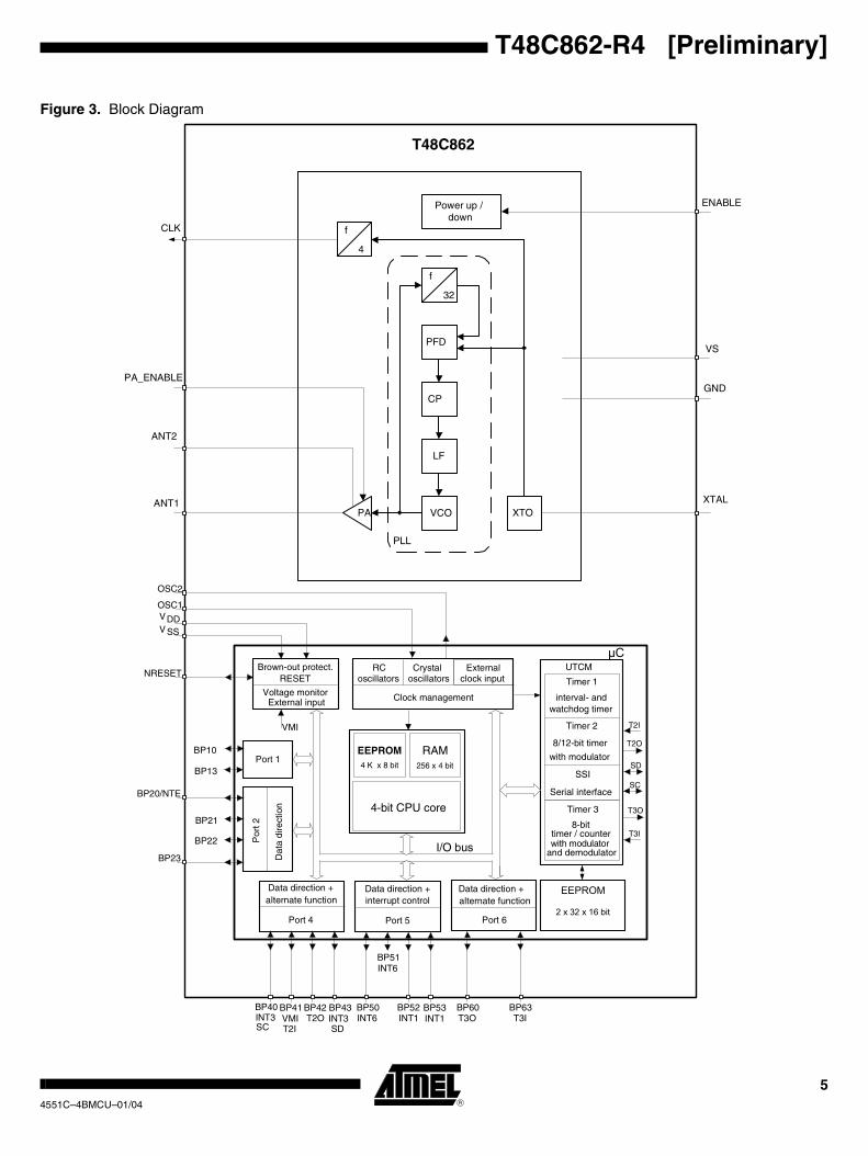
Figure 3. Block Diagram
CLK
PA_ENABLE
ANT2
ANT1
ENABLE
GND
VS
XTALVCO
LF
CP
PFD
f
32
XTO
PLL
PA
f
4
Power up / down
Voltage monitor External input
UTCM
OSC1
OSC2
I/O bus
EEPROM RAM
4-bit CPU core
256 x 4 bit
Data direction +alternate function
Data direction +interrupt control
Port 4 Port 5
Data direction +alternate function
Port 6
Timer 3
Brown-out protect.RESET
Clock management
Timer 1
watchdog timer
Timer 2
Serial interface
Port 1
Por
t 2
Dat
a di
rect
ion
T2O
SD
SC
T3O
T3I
BP10
BP13
BP20/NTE
BP21
BP22
BP23
RCoscillators
Crystaloscillators
4 K x 8 bit
VMI
with modulator
SSI
Externalclock input
interval- and
8/12-bit timer
8-bittimer / counterwith modulator
and demodulator
T2I
EEPROM
2 x 32 x 16 bit
BP40INT3 SC T2I
BP41 VMI
SD
BP43INT3
BP42 T2O
BP53INT1
BP52INT1
BP50INT6
BP51INT6
BP60 T3O
BP63 T3I
V SS
VDD
NRESET
µC
T48C862
6 T48C862-R4 [Preliminary] 4551C–4BMCU–01/04
General Description The fully-integrated PLL transmitter that allows particularly simple, low-cost RF minia-ture transmitters to be assembled. The VCO is locked to 32 × fXTAL, thus, a 13.56 MHzcrystal is needed for a 433.92 MHz transmitter. All other PLL and VCO peripheral ele-ments are integrated.
The XTO is a series resonance oscillator so that only one capacitor together with acrystal connected in series to GND are needed as external elements.
The crystal oscillator together with the PLL needs maximum < 1 ms until the PLL islocked and the CLK output is stable. A wait time of ≥ 1 ms until the CLK is used for themicrocontroller and the PA is switched on.
The power amplifier is an open-collector output delivering a current pulse which is nearlyindependent from the load impedance. The delivered output power is controllaed via theconnected load impedance.
This output configuration enables a simple matching to any kind of antenna or to 50 Ω. Ahigh power efficiency of η= Pout/(IS,PA × VS) of 36% for the power amplifier results whenan optimized load impedance of ZLoad = (166 + j223) Ω is used at 3 V supply voltage.
Functional Description
If ENABLE = L and PA_ENABLE = L, the circuit is in standby mode consuming only avery small amount of current so that a lithium cell used as power supply can work forseveral years.
With ENABLE = H, the XTO, PLL and the CLK driver are switched on. If PA_ENABLEremains L, only the PLL and the XTO are running and the CLK signal is delivered to themicrocontroller. The VCO locks to 32 times the XTO frequency.
With ENABLE = H and PA_ENABLE = H, the PLL, XTO, CLK driver and the poweramplifier are on. With PA_ENABLE, the power amplifier can be switched on and off,which is used to perform the ASK modulation.
ASK Transmission The PLL transmitter block is activated by ENABLE = H. PA_ENABLE must remain L fort ≥ 1 ms, then the CLK signal can be taken to clock the microcontroller and the outputpower can be modulated by means of pin PA_ENABLE. After transmission,PA_ENABLE is switched to L and the microcontroller switches back to internal clocking.The PLL transmitter block is switched back to standby mode with ENABLE = L.
FSK Transmission The PLL transmitter block is activated by ENABLE = H. PA_ENABLE must remain L fort ≥ 1 ms, then the CLK signal can be taken to clock the microcontroller and the poweramplifier is switched on with PA_ENABLE = H. The chip is then ready for FSK modula-tion. The microcontroller starts to switch on and off the capacitor between the XTAL loadcapacitor and GND with an open-drain output port, thus changing the referencefrequency of the PLL. If the switch is closed, the output frequency is lower than if theswitch is open. After transmission PA_ENABLE is switched to L and the microcontrollerswitches back to internal clocking. The PLL transmitter block is switched back tostandby mode with ENABLE = L.
The accuracy of the frequency deviation with XTAL pulling method is about ±25% whenthe following tolerances are considered.
7
T48C862-R4 [Preliminary]
4551C–4BMCU–01/04
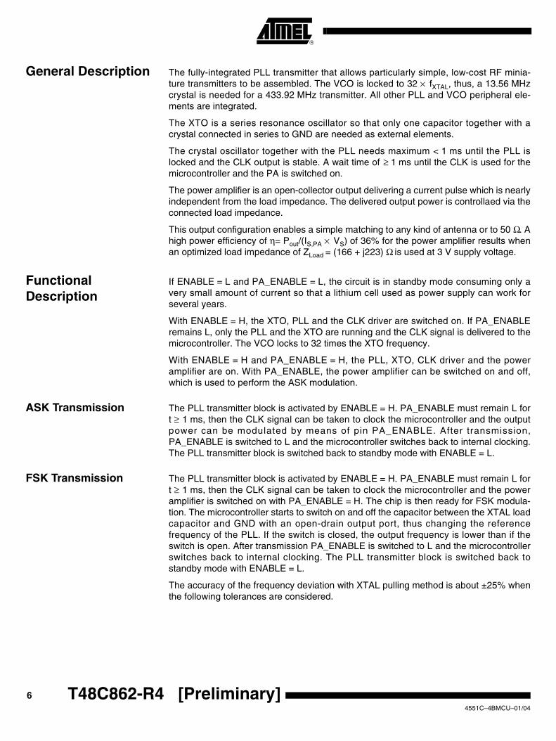
Figure 4. Tolerances of Frequency Modulation
Using C4 = 9.2 pF ±2%, C5 = 6.8 pF ±5%, a switch port with CSwitch = 3 pF ±10%, straycapacitances on each side of the crystal of CStray1 = CStray2 = 1 pF ±10%, a parallelcapacitance of the crystal of C0 = 3.2 pF ±10% and a crystal with CM = 13 fF ±10%, anFSK deviation of ±21 kHz typical with worst case tolerances of ±16.3 kHz to ±28.8 kHzresults.
CLK Output An output CLK signal is provided for a connected microcontroller. The delivered signal isCMOS compatible if the load capacitance is lower than 10 pF.
Clock Pulse Take Over The clock of the crystal oscillator can be used for clocking the microcontroller. the micro-controller block has the special feature of starting with an integrated RC-oscillator toswitch on the PLL transmitter block with ENABLE = H, and after 1 ms to assume theclock signal of the transmission IC, so the message can be sent with crystal accuracy.
Output Matching and Power Setting
The output power is set by the load impedance of the antenna. The maximum outputpower is achieved with a load impedance of ZLoad,opt = (166 + j223) Ω. There must be alow resistive path to VS to deliver the DC current.
The delivered current pulse of the power amplifier is 9 mA and the maximum outputpower is delivered to a resistive load of 465 Ω if the 1.0 pF output capacitance of thepower amplifier is compensated by the load impedance.
An optimum load impedance of:ZLoad = 465 Ω || j/(2 × π 1.0 pF) = (166 + j223) Ω thus results for the maximum outputpower of 7.5 dBm.
The load impedance is defined as the impedance seen from the PLL transmitter block’sANT1, ANT2 into the matching network. Do not confuse this large signal load imped-ance with a small signal input impedance delivered as input characteristic of RFamplifiers and measured from the application into the IC instead of from the IC into theapplication for a power amplifier.
Less output power is achieved by lowering the real parallel part of 465 Ω where theparallel imaginary part should be kept constant.
Output power measurement can be done with the circuit shown in Figure 5 on page 8.Note that the component values must be changed to compensate the individual boardparas i t ics unt i l the PLL t ransmi t te r b lock has the r igh t load impedanceZLoad,opt = (166 + j223) Ω. Also the damping of the cable used to measure the outputpower must be calibrated.
~
~
VS
XTALCStray1
CM LM RS
C0
CStray2
C4
C5
Crystal equivalent circuit CSwitch
8 T48C862-R4 [Preliminary] 4551C–4BMCU–01/04
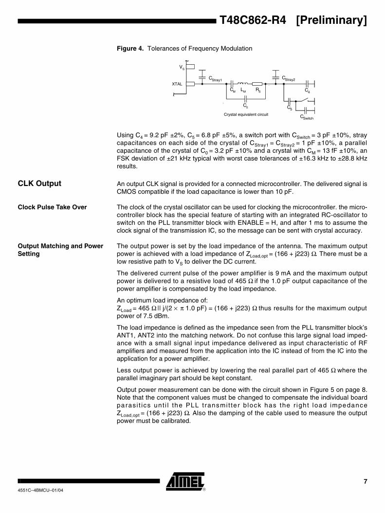
Figure 5. Output Power Measurement
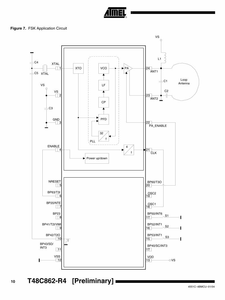
Application Circuit For the supply-voltage blocking capacitor C3, a value of 68 nF/X7R is recommended(see Figure 6 on page 9 and Figure 7 on page 10). C1 and C2 are used to match the loopantenna to the power amplifier where C1 typically is 8.2 pF/NP0 and C2 is 6 pF/NP0(10 pF + 15 pF in series); for C2 two capacitors in series should be used to achieve abetter tolerance value and to have the possibility to realize the ZLoad,opt by using stan-dard valued capacitors.
C1 forms together with the pins of PLL transmitter block and the PCB board wires aseries resonance loop that suppresses the 1st harmonic, thus, the position of C1 on thePCB is important. Normally the best suppression is achieved when C1 is placed as closeas possible to the pins ANT1 and ANT2.
The loop antenna should not exceed a width of 1.5 mm, otherwise the Q-factor of theloop antenna is too high.
L1 (≈ 50 nH to 100 nH) can be printed on PCB. C4 should be selected so the XTO runson the load resonance frequency of the crystal. Normally, a value of 12 pF results for a15 pF load-capacitance crystal.
~
~
ANT2
ANT1
Rin
Powermeter
C1 = 1n
L1 = 33n
C2 = 2.2pZLopt
VS
Z = 50 Ω
50 Ω

9
T48C862-R4 [Preliminary]
4551C–4BMCU–01/04
Figure 6. ASK Application Circuit
CLK
PA_ENABLE
ANT2
ANT1
ENABLE
GND
VS
XTAL
21
22
23
241
2
3
4
VCO
LF
CP
PFD
f
32
XTO
PLL
PA
f
4
Power up/down
C3
VSC1
VS
C4
LoopAntenna
L1
XTAL
C2
9
11
6
5
8
7
10
12
BP20/NTE
VDD
BP42/T2O
VSS
15
16
17
13
19
20
18
17
OSC1
OSC2
BP60/T3O
BP50/INT6
BP63/T3I
BP23
NRESET
BP41/T2I/VMI
BP43/SD/INT3
BP52/INT1
BP53/INT1
BP40/SC/INT3
VS
S1
S2
S3
10 T48C862-R4 [Preliminary] 4551C–4BMCU–01/04
Figure 7. FSK Application Circuit
CLK
PA_ENABLE
ANT2
ANT1
ENABLE
GND
VS
XTAL
21
22
23
241
2
3
4
VCO
LF
CP
PFD
f
32
XTO
PLL
PA
f
4
Power up/down
C3
VSC1
VS
C4
LoopAntenna
L1
XTAL
C2
C5
9
11
6
5
8
7
10
12
BP20/NTE
VDD
BP42/T2O
VSS
15
16
17
13
19
20
18
17
OSC1
OSC2
BP60/T3O
BP50/INT6
BP63/T3I
BP23
NRESET
BP41/T2I/VMI
BP43/SD/INT3
BP52/INT1
BP53/INT1
BP40/SC/INT3
VS
S1
S2
S3
11
T48C862-R4 [Preliminary]
4551C–4BMCU–01/04
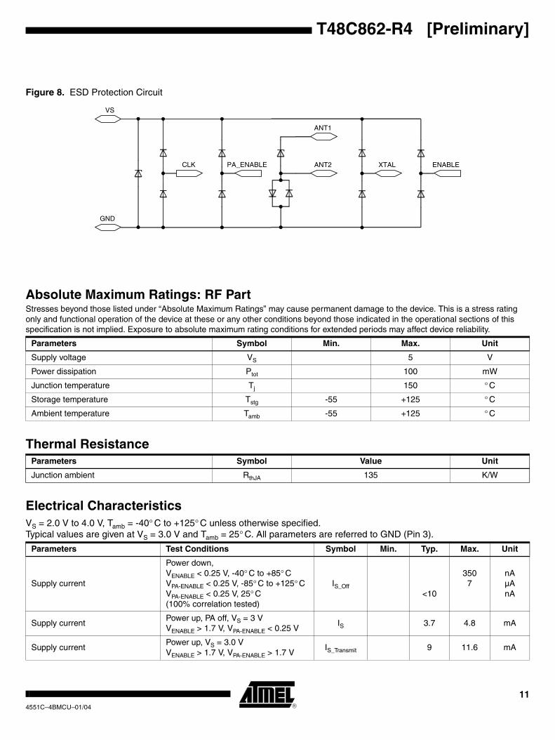
Figure 8. ESD Protection Circuit
CLK PA_ENABLE ANT2
ANT1
XTAL ENABLE
VS
GND
Absolute Maximum Ratings: RF PartStresses beyond those listed under “Absolute Maximum Ratings” may cause permanent damage to the device. This is a stress rating only and functional operation of the device at these or any other conditions beyond those indicated in the operational sections of this specification is not implied. Exposure to absolute maximum rating conditions for extended periods may affect device reliability.
Parameters Symbol Min. Max. Unit
Supply voltage VS 5 V
Power dissipation Ptot 100 mW
Junction temperature Tj 150 ° C
Storage temperature Tstg -55 +125 ° C
Ambient temperature Tamb -55 +125 ° C
Thermal ResistanceParameters Symbol Value Unit
Junction ambient RthJA 135 K/W
Electrical CharacteristicsVS = 2.0 V to 4.0 V, Tamb = -40° C to +125° C unless otherwise specified. Typical values are given at VS = 3.0 V and Tamb = 25° C. All parameters are referred to GND (Pin 3).
Parameters Test Conditions Symbol Min. Typ. Max. Unit
Supply current
Power down, VENABLE < 0.25 V, -40° C to +85° CVPA-ENABLE < 0.25 V, -85° C to +125° CVPA-ENABLE < 0.25 V, 25° C (100% correlation tested)
IS_Off<10
3507
nAµAnA
Supply currentPower up, PA off, VS = 3 VVENABLE > 1.7 V, VPA-ENABLE < 0.25 V
IS 3.7 4.8 mA
Supply currentPower up, VS = 3.0 VVENABLE > 1.7 V, VPA-ENABLE > 1.7 V
IS_Transmit 9 11.6 mA

12 T48C862-R4 [Preliminary] 4551C–4BMCU–01/04
Output powerVS = 3.0 V, Tamb = 25° Cf = 433.92 MHz, ZLoad = (166 + j233) Ω PRef 5.5 7.5 10 dBm
Output power variation for the full temperature range
Tamb = -40° C to +85° CVS = 3.0 VVS = 2.0 V
∆PRef∆PRef
-1.5-4.0
dBdB
Output power variation for the full temperature range
Tamb = -40° C to +125° CVS = 3.0 VVS = 2.0 VPOut = PRef + ∆PRef
∆PRef∆PRef
-2.0-4.5
dBdB
Achievable output-power range Selectable by load impedance POut_typ 0 7.5 dBm
Spurious emission
fCLK = f0/128Load capacitance at Pin CLK = 10 pFfO ± 1× fCLK fO ± 4 × fCLK other spurious are lower
-55-52
dBcdBc
Oscillator frequency XTO (= phase comparator frequency)
fXTO = f0/32fXTAL = resonant frequency of the XTAL, CM ≤ 10 fF, load capacitance selected accordingly Tamb = -40° C to +85° CTamb = -40° C to +125° C
fXTO
-30-40
fXTAL +30+40
ppmppm
PLL loop bandwidth 250 kHz
Phase noise of phase comparator
Referred to fPC = fXT0,25 kHz distance to carrier
-116 -110 dBc/Hz
In loop phase noise PLL 25 kHz distance to carrier -86 -80 dBc/Hz
Phase noise VCOat 1 MHzat 36 MHz
-94-125
-90-121
dBc/HzdBc/Hz
Frequency range of VCO fVCO 429 439 MHz
Clock output frequency (CMOS microcontroller compatible)
f0/128 MHz
Voltage swing at Pin CLK CLoad ≤ 10 pFV0hV0l
VS × 0.8 VS × 0.
2
VV
Series resonance R of the crystal Rs 110 Ω
Capacitive load at Pin XT0 7 pF
FSK modulation frequency rateDuty cycle of the modulation signal = 50%
0 32 kHz
ASK modulation frequency rateDuty cycle of the modulation signal = 50%
0 32 kHz
ENABLE input Low level input voltageHigh level input voltageInput current high
VIlVIhIIn
1.70.25
20
VV
µA
PA_ENABLE input Low level input voltageHigh level input voltageInput current high
VIlVIhIIn
1.70.25
5
VV
µA
Electrical Characteristics (Continued)VS = 2.0 V to 4.0 V, Tamb = -40° C to +125° C unless otherwise specified. Typical values are given at VS = 3.0 V and Tamb = 25° C. All parameters are referred to GND (Pin 3).
Parameters Test Conditions Symbol Min. Typ. Max. Unit
13
T48C862-R4 [Preliminary]
4551C–4BMCU–01/04
Microcontroller Block
Features • 4-Kbyte ROM, 256 x 4-bit RAM• EEPROM Programmable Options• Read Protection for the EEPROM Program Memory• 11 Bi-directional I/Os• Up to Seven External/Internal Interrupt Sources• Eight Hardware and Software Interrupt Priorities• Multifunction Timer/Counter
- IR Remote Control Carrier Generator- Biphase-, Manchester- and Pulse-width Modulator and Demodulator- Phase Control Function
• Programmable System Clock with Prescaler and Five Different Clock Sources• Very Low Sleep Current (< 1 µA)• 2 × 512-bit EEPROM Data Memory• 256 × 4-bit RAM Data Memory• Synchronous Serial Interface (2-wire, 3-wire)• Watchdog, POR and Brown-out Function• Voltage Monitoring Inclusive Lo_BAT Detect
Description The microcontroller is designed with EEPROM cells so it can be programmed severaltimes. To offer full compatibility with each ROM version, the I/O configuration is storedinto a separate internal EEPROM block during programming. The configuration is down-loaded to the I/Os with every power-on reset.
Introduction The microcontroller block is a member of Atmel’s family of 4-bit single-chip microcontrol-lers. Instead of ROM it contains EEPROM, RAM, parallel I/O ports, two 8-bitprogrammable multifunction timer/counters, voltage supervisor, interval timer withwatchdog function and a sophisticated on-chip clock generation with integrated RC-,32-kHz and 4-MHz crystal oscillators.
Differences between T48C862-R4 and ATAR862 Microcontrollers
Program Memory The program memory of the devices is realized as an EEPROM. The memory size foruser programs is 4096 bytes. It is programmed as 258 × 16 bytes blocks of data. theimplement LOCK-bit function is user-selectable and protects the device from unautho-rized read-out of the program memory.
Configuration Memory An additional area of 32 bytes of the EEPROM is used to store information about thehardware configuration. All the options that are selectable for the ROM versions areavailable to the user. This includes not only the different port options but also the possi-bilities to select different capacitors for OSC1 and OSC2, the option to enable or disablethe hardlock for the watchdog, the option to select OSC2 instead of OSC1 as externalclock input and the option to enable the external clock monitor as a reset source.
Data Memory The microcontroller block contains an internal data EEPROM that is organized as twopages of 32 × 16-bit. To be compatible with the ROM parts, the page used has to bedefined within the application software by writing the 2-wire interface (TWI) command"09h" to the EEPROM. This command has no effect for the microcontroller block, if it isleft inside the HEX-file for the ROM version. Also for compatibility reasons, the access tothe EEPROM is handled via the MCL (serial interface) as in the corresponding ROMparts.
14 T48C862-R4 [Preliminary] 4551C–4BMCU–01/04
Reset Function During each reset (power-on or brown-out), the I/O configuration is deleted andreloaded with the data from the configuration memory. This leads to a slightly differentbehavior compared to the ROM versions. Both devices switch their I/Os to input duringreset but the ROM part has the mask selected pull-up or pull-down resistors active whilethe MTP has them removed until the download is finished.
MARC4 Architecture General Description
The microcontroller consists of an advanced stack-based, 4-bit CPU core and on-chipperipherals. The CPU is based on the Harvard architecture with physically separatedprogram memory (ROM) and data memory (RAM). Three independent buses, theinstruction bus, the memory bus and the I/O bus, are used for parallel communicationbetween ROM, RAM and peripherals. This enhances program execution speed byallowing both instruction prefetching, and a simultaneous communication to the on-chipperipheral circuitry. The extremely powerful integrated interrupt controller with associ-ated eight prioritized interrupt levels supports fast and efficient processing of hardwareevents. The microcontroller is designed for the high-level programming languageqFORTH. The core includes both an expression and a return stack. This architectureenables high-level language programming without any loss of efficiency or code density.
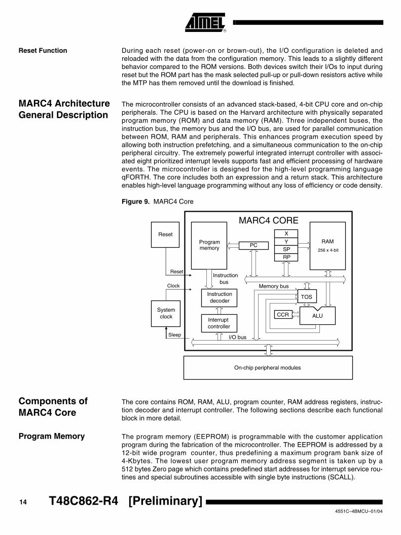
Figure 9. MARC4 Core
Components of MARC4 Core
The core contains ROM, RAM, ALU, program counter, RAM address registers, instruc-tion decoder and interrupt controller. The following sections describe each functionalblock in more detail.
Program Memory The program memory (EEPROM) is programmable with the customer applicationprogram during the fabrication of the microcontroller. The EEPROM is addressed by a12-bit wide program counter, thus predefining a maximum program bank size of4-Kbytes. The lowest user program memory address segment is taken up by a512 bytes Zero page which contains predefined start addresses for interrupt service rou-tines and special subroutines accessible with single byte instructions (SCALL).
Instruction decoder
CCR
TOS
ALU
RAM
RP
X
YProgram256 x 4-bit
MARC4 CORE
Clock
Reset
Sleep
Memory bus
I/O bus
Instruction bus
Reset
System clock
Interruptcontroller
On-chip peripheral modules
memory SPPC
15
T48C862-R4 [Preliminary]
4551C–4BMCU–01/04
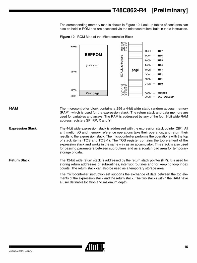
The corresponding memory map is shown in Figure 10. Look-up tables of constants canalso be held in ROM and are accessed via the microcontrollers’ built-in table instruction.
Figure 10. ROM Map of the Microcontroller Block
RAM The microcontroller block contains a 256 x 4-bit wide static random access memory(RAM), which is used for the expression stack. The return stack and data memory areused for variables and arrays. The RAM is addressed by any of the four 8-bit wide RAMaddress registers SP, RP, X and Y.
Expression Stack The 4-bit wide expression stack is addressed with the expression stack pointer (SP). Allarithmetic, I/O and memory reference operations take their operands, and return theirresults to the expression stack. The microcontroller performs the operations with the topof stack items (TOS and TOS-1). The TOS register contains the top element of theexpression stack and works in the same way as an accumulator. This stack is also usedfor passing parameters between subroutines and as a scratch pad area for temporarystorage of data.
Return Stack The 12-bit wide return stack is addressed by the return stack pointer (RP). It is used forstoring return addresses of subroutines, interrupt routines and for keeping loop indexcounts. The return stack can also be used as a temporary storage area.
The microcontroller instruction set supports the exchange of data between the top ele-ments of the expression stack and the return stack. The two stacks within the RAM havea user definable location and maximum depth.
EEPROM
(4 K x 8 bit)
Zero page
FFFh
7FFh
1FFh
000h
1F0h1F8h
010h018h
000h008h
020h
1E8h1E0h
SC
ALL
add
ress
es
140h
180h
040h
0C0h
008h $AUTOSLEEP
$RESET
INT0
INT1
INT2
INT3
INT4
INT5
INT6
INT71E0h
1C0h
100h
080h
page
000h

16 T48C862-R4 [Preliminary] 4551C–4BMCU–01/04
Figure 11. RAM Map
Registers The microcontroller has seven programmable registers and one condition code register(see Figure 12).
Program Counter (PC) The program counter is a 12-bit register which contains the address of the next instruc-tion to be fetched from the EEPROM. Instructions currently being executed are decodedin the instruction decoder to determine the internal micro-operations. For linear code (nocalls or branches), the program counter is incremented with every instruction cycle. If abranch-, call-, return-instruction or an interrupt is executed, the program counter isloaded with a new address. The program counter is also used with the table instructionto fetch 8-bit wide EEPROM constants.
Figure 12. Programming Mode l
RAM
FCh
00h
Autosleep
FFh
03h04h
X
Y
SP
RP
TOS-1
Expressionstack
Returnstack
Globalvariables
RA
M a
ddre
ss r
egis
ter:
07h
(256 x 4-bit)
Globalvariables
4-bit
TOSTOS-1TOS-2
3 0
SP
Expression stack
Return stack011
12-bit
RP
v
TOS
CCR
03
03
07
07
7
011
RP
SP
X
Y
PC
-- B I
Program counter
Return stack pointer
Expression stack pointer
RAM address register (X)
RAM address register (Y)
Top of stack register
Condition code register
Carry / borrow
BranchInterrupt enable
Reserved
07
C
0
00

17
T48C862-R4 [Preliminary]
4551C–4BMCU–01/04
RAM Address Registers The RAM is addressed with the four 8-bit wide RAM address registers: SP, RP, X and Y.These registers allow access to any of the 256 RAM nibbles.
Expression Stack Pointer (SP) The stack pointer contains the address of the next-to-top 4-bit item (TOS-1) of theexpression stack. The pointer is automatically pre-incremented if a nibble is moved ontothe stack or post-decremented if a nibble is removed from the stack. Every post-decre-ment operation moves the item (TOS-1) to the TOS register before the SP isdecremented. After a reset, the stack pointer has to be initialized with >SP S0 to allocatethe start address of the expression stack area.
Return Stack Pointer (RP) The return stack pointer points to the top element of the 12-bit wide return stack. Thepointer automatically pre-increments if an element is moved onto the stack, or it post-decrements if an element is removed from the stack. The return stack pointer incre-ments and decrements in steps of 4. This means that every time a 12-bit element isstacked, a 4-bit RAM location is left unwritten. This location is used by the qFORTHcompiler to allocate 4-bit variables. After a reset the return stack pointer has to be initial-ized via >RP FCh.
RAM Address Registers (X and Y)
The X and Y registers are used to address any 4-bit item in the RAM. A fetch operationmoves the addressed nibble onto the TOS. A store operation moves the TOS to theaddressed RAM location. By using either the pre-increment or post-decrement address-ing mode arrays in the RAM can be compared, filled or moved.
Top of Stack (TOS) The top of stack register is the accumulator of the microcontroller block. All arith-metic/logic, memory reference and I/O operations use this register. The TOS registerreceives data from the ALU, EEPROM, RAM or I/O bus.
Condition Code Register (CCR)
The 4-bit wide condition code register contains the branch, the carry and the interruptenable flag. These bits indicate the current state of the CPU. The CCR flags are set orreset by ALU operations. The instructions SET_BCF, TOG_BF, CCR! and DI allowdirect manipulation of the condition code register.
Carry/Borrow (C) The carry/borrow flag indicates that the borrowing or carrying out of arithmetic logic unit(ALU) occurred during the last arithmetic operation. During shift and rotate operations,this bit is used as a fifth bit. Boolean operations have no effect on the C-flag.
Branch (B) The branch flag controls the conditional program branching. Should the branch flag hasbeen set by a previous instruction, a conditional branch will cause a jump. This flag isaffected by arithmetic, logic, shift, and rotate operations.
Interrupt Enable (I) The interrupt enable flag globally enables or disables the triggering of all interrupt rou-tines with the exception of the non-maskable reset. After a reset or while executing theDI instruction, the interrupt enable flag is reset, thus disabling all interrupts. The core willnot accept any further interrupt requests until the interrupt enable flag has been setagain by either executing an EI or SLEEP instruction.
18 T48C862-R4 [Preliminary] 4551C–4BMCU–01/04
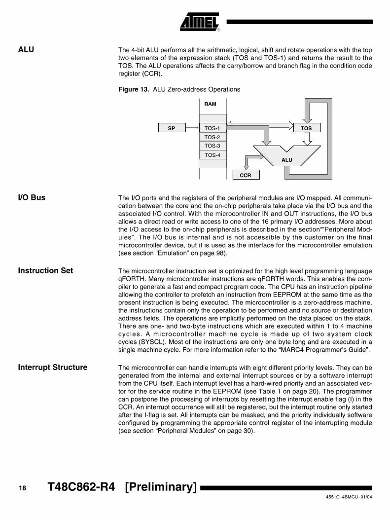
ALU The 4-bit ALU performs all the arithmetic, logical, shift and rotate operations with the toptwo elements of the expression stack (TOS and TOS-1) and returns the result to theTOS. The ALU operations affects the carry/borrow and branch flag in the condition coderegister (CCR).
Figure 13. ALU Zero-address Operations
I/O Bus The I/O ports and the registers of the peripheral modules are I/O mapped. All communi-cation between the core and the on-chip peripherals take place via the I/O bus and theassociated I/O control. With the microcontroller IN and OUT instructions, the I/O busallows a direct read or write access to one of the 16 primary I/O addresses. More aboutthe I/O access to the on-chip peripherals is described in the section“”Peripheral Mod-ules”. The I/O bus is internal and is not accessible by the customer on the finalmicrocontroller device, but it is used as the interface for the microcontroller emulation(see section “Emulation” on page 98).
Instruction Set The microcontroller instruction set is optimized for the high level programming languageqFORTH. Many microcontroller instructions are qFORTH words. This enables the com-piler to generate a fast and compact program code. The CPU has an instruction pipelineallowing the controller to prefetch an instruction from EEPROM at the same time as thepresent instruction is being executed. The microcontroller is a zero-address machine,the instructions contain only the operation to be performed and no source or destinationaddress fields. The operations are implicitly performed on the data placed on the stack.There are one- and two-byte instructions which are executed within 1 to 4 machinecycles. A microcontro l ler machine cycle is made up of two system clockcycles (SYSCL). Most of the instructions are only one byte long and are executed in asingle machine cycle. For more information refer to the “MARC4 Programmer’s Guide”.
Interrupt Structure The microcontroller can handle interrupts with eight different priority levels. They can begenerated from the internal and external interrupt sources or by a software interruptfrom the CPU itself. Each interrupt level has a hard-wired priority and an associated vec-tor for the service routine in the EEPROM (see Table 1 on page 20). The programmercan postpone the processing of interrupts by resetting the interrupt enable flag (I) in theCCR. An interrupt occurrence will still be registered, but the interrupt routine only startedafter the I-flag is set. All interrupts can be masked, and the priority individually softwareconfigured by programming the appropriate control register of the interrupting module(see section “Peripheral Modules” on page 30).
TOS-1
CCR
RAM
TOS-2
SP
TOS-3
TOS
ALUTOS-4

19
T48C862-R4 [Preliminary]
4551C–4BMCU–01/04
Interrupt Processing For processing the eight interrupt levels, the microcontroller includes an interrupt con-troller with two 8-bit wide interrupt pending and interrupt active registers. The interruptcontroller samples all interrupt requests during every non-I/O instruction cycle andlatches these in the interrupt pending register. If no higher priority interrupt is present inthe interrupt active register, it signals the CPU to interrupt the current program execu-tion. If the interrupt enable bit is set, the processor enters an interrupt acknowledgecycle. During this cycle a short call (SCALL) instruction to the service routine is exe-cuted and the current PC is saved on the return stack. An interrupt service routine iscompleted with the RTI instruction. This instruction resets the corresponding bits in theinterrupt pending/active register and fetches the return address from the return stack tothe program counter. When the interrupt enable flag is reset (triggering of interrupt rou-tines is disabled), the execution of new interrupt service routines is inhibited but not thelogging of the interrupt requests in the interrupt pending register. The execution of theinterrupt is delayed until the interrupt enable flag is set again. Note that interrupts areonly lost if an interrupt request occurs while the corresponding bit in the pending registeris still set (i.e., the interrupt service routine is not yet finished).
It should be noted that automatic stacking of the RBR is not carried out by the hardwareand so if ROM banking is used, the RBR must be stacked on the expression stack bythe application program and restored before the RTI. After a master reset (power-on,brown-out or watchdog reset), the interrupt enable flag and the interrupt pending andinterrupt active register are all reset.
Interrupt Latency The interrupt latency is the time from the occurrence of the interrupt to the interruptservice routine being activated. This is extremely short (taking between 3 to 5 machinecycles depending on the state of the core).
Figure 14. Interrupt Handling
7
6
5
4
3
2
1
0
Pri
ori
ty le
vel
INT5 active
INT7 active
INT2 pending
SWI0
INT2 active
INT0 pending INT0 active
INT2
RTI
RTIINT5
INT3 active
INT3
RTI
RTI
RTI
INT7
Time
Main /Autosleep
Main /Autosleep
20 T48C862-R4 [Preliminary] 4551C–4BMCU–01/04
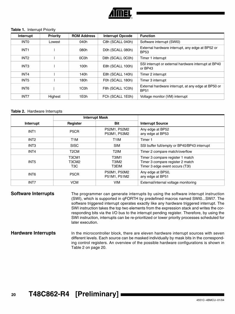
Table 1. Interrupt Priority
Table 2. Hardware Interrupts
Software Interrupts The programmer can generate interrupts by using the software interrupt instruction(SWI), which is supported in qFORTH by predefined macros named SWI0...SWI7. Thesoftware triggered interrupt operates exactly like any hardware triggered interrupt. TheSWI instruction takes the top two elements from the expression stack and writes the cor-responding bits via the I/O bus to the interrupt pending register. Therefore, by using theSWI instruction, interrupts can be re-prioritized or lower priority processes scheduled forlater execution.
Hardware Interrupts In the microcontroller block, there are eleven hardware interrupt sources with sevendifferent levels. Each source can be masked individually by mask bits in the correspond-ing control registers. An overview of the possible hardware configurations is shown inTable 2 on page 20.
Interrupt Priority ROM Address Interrupt Opcode Function
INT0 Lowest 040h C8h (SCALL 040h) Software interrupt (SWI0)
INT1 | 080h D0h (SCALL 080h)External hardware interrupt, any edge at BP52 or BP53
INT2 | 0C0h D8h (SCALL 0C0h) Timer 1 interrupt
INT3 | 100h E8h (SCALL 100h)SSI interrupt or external hardware interrupt at BP40 or BP43
INT4 | 140h E8h (SCALL 140h) Timer 2 interrupt
INT5 | 180h F0h (SCALL 180h) Timer 3 interrupt
INT6 | 1C0h F8h (SCALL 1C0h)External hardware interrupt, at any edge at BP50 or BP51
INT7 Highest 1E0h FCh (SCALL 1E0h) Voltage monitor (VM) interrupt
Interrupt
Interrupt Mask
Interrupt SourceRegister Bit
INT1 P5CRP52M1, P52M2P53M1, P53M2
Any edge at BP52any edge at BP53
INT2 T1M T1IM Timer 1
INT3 SISC SIM SSI buffer full/empty or BP40/BP43 interrupt
INT4 T2CM T2IM Timer 2 compare match/overflow
INT5T3CM1T3CM2
T3C
T3IM1T3IM2T3EIM
Timer 3 compare register 1 matchTimer 3 compare register 2 matchTimer 3 edge event occurs (T3I)
INT6 P5CRP50M1, P50M2P51M1, P51M2
Any edge at BP50,any edge at BP51
INT7 VCM VIM External/internal voltage monitoring
21
T48C862-R4 [Preliminary]
4551C–4BMCU–01/04
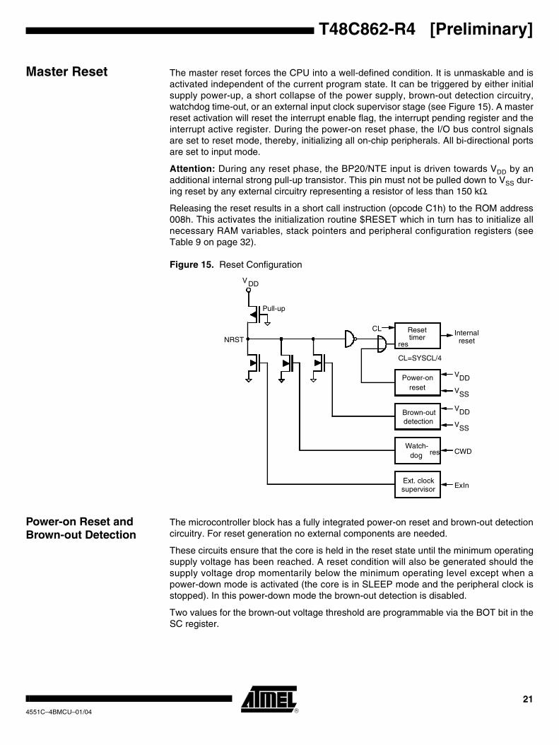
Master Reset The master reset forces the CPU into a well-defined condition. It is unmaskable and isactivated independent of the current program state. It can be triggered by either initialsupply power-up, a short collapse of the power supply, brown-out detection circuitry,watchdog time-out, or an external input clock supervisor stage (see Figure 15). A masterreset activation will reset the interrupt enable flag, the interrupt pending register and theinterrupt active register. During the power-on reset phase, the I/O bus control signalsare set to reset mode, thereby, initializing all on-chip peripherals. All bi-directional portsare set to input mode.
Attention: During any reset phase, the BP20/NTE input is driven towards VDD by anadditional internal strong pull-up transistor. This pin must not be pulled down to VSS dur-ing reset by any external circuitry representing a resistor of less than 150 kΩ.
Releasing the reset results in a short call instruction (opcode C1h) to the ROM address008h. This activates the initialization routine $RESET which in turn has to initialize allnecessary RAM variables, stack pointers and peripheral configuration registers (seeTable 9 on page 32).
Figure 15. Reset Configuration
Power-on Reset and Brown-out Detection
The microcontroller block has a fully integrated power-on reset and brown-out detectioncircuitry. For reset generation no external components are needed.
These circuits ensure that the core is held in the reset state until the minimum operatingsupply voltage has been reached. A reset condition will also be generated should thesupply voltage drop momentarily below the minimum operating level except when apower-down mode is activated (the core is in SLEEP mode and the peripheral clock isstopped). In this power-down mode the brown-out detection is disabled.
Two values for the brown-out voltage threshold are programmable via the BOT bit in theSC register.
Resettimer
VDD
CL
Power-onreset
Internalresetres
CL=SYSCL/4
VDD
VSS
Brown-outdetection
VDD
VSS
Watch-dog CWDres
Ext. clocksupervisor ExIn
Pull-up
NRST
22 T48C862-R4 [Preliminary] 4551C–4BMCU–01/04
A power-on reset pulse is generated by a VDD rise across the default BOT voltage level(1.7 V). A brown-out reset pulse is generated when VDD falls below the brown-out volt-age threshold. Two values for the brown-out voltage threshold are programmable viathe BOT bit in the SC register. When the controller runs in the upper supply voltagerange with a high system clock frequency, the high threshold must be used. When itruns with a lower system clock frequency, the low threshold and a wider supply voltagerange may be chosen. For further details, see the electrical specification and theSC register description for BOT programming.
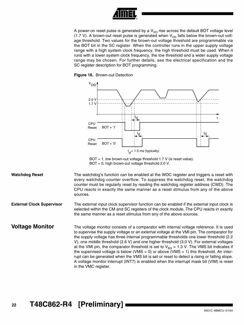
Figure 16. Brown-out Detection
Watchdog Reset The watchdog’s function can be enabled at the WDC register and triggers a reset withevery watchdog counter overflow. To suppress the watchdog reset, the watchdogcounter must be regularly reset by reading the watchdog register address (CWD). TheCPU reacts in exactly the same manner as a reset stimulus from any of the abovesources.
External Clock Supervisor The external input clock supervisor function can be enabled if the external input clock isselected within the CM and SC registers of the clock module. The CPU reacts in exactlythe same manner as a reset stimulus from any of the above sources.
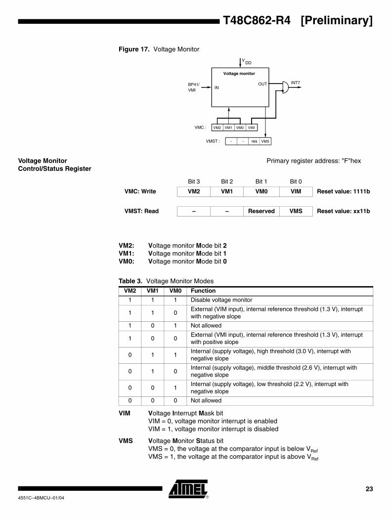
Voltage Monitor The voltage monitor consists of a comparator with internal voltage reference. It is usedto supervise the supply voltage or an external voltage at the VMI pin. The comparator forthe supply voltage has three internal programmable thresholds one lower threshold (2.2V), one middle threshold (2.6 V) and one higher threshold (3.0 V). For external voltagesat the VMI pin, the comparator threshold is set to VBG = 1.3 V. The VMS bit indicates ifthe supervised voltage is below (VMS = 0) or above (VMS = 1) this threshold. An inter-rupt can be generated when the VMS bit is set or reset to detect a rising or falling slope.A voltage monitor interrupt (INT7) is enabled when the interrupt mask bit (VIM) is resetin the VMC register.
VDD
CPUReset
t
BOT = '1'
2.0 V1.7 V
CPUReset BOT = '0'
td td
td= 1.5 ms (typically)
td
BOT = 1, low brown-out voltage threshold 1.7 V (is reset value).BOT = 0, high brown-out voltage threshold 2.0 V.
23
T48C862-R4 [Preliminary]
4551C–4BMCU–01/04
Figure 17. Voltage Monitor
Voltage Monitor Control/Status Register
Primary register address: "F"hex
VM2: Voltage monitor Mode bit 2VM1: Voltage monitor Mode bit 1VM0: Voltage monitor Mode bit 0
Table 3. Voltage Monitor Modes
VIM Voltage Interrupt Mask bitVIM = 0, voltage monitor interrupt is enabledVIM = 1, voltage monitor interrupt is disabled
VMS Voltage Monitor Status bitVMS = 0, the voltage at the comparator input is below VRefVMS = 1, the voltage at the comparator input is above VRef
VDD
VM2
Voltage monitor
VM1 VM0 VIM
VMS - - res
OUTIN
BP41/VMI
INT7
VMC :
VMST :
Bit 3 Bit 2 Bit 1 Bit 0
VMC: Write VM2 VM1 VM0 VIM Reset value: 1111b
VMST: Read – – Reserved VMS Reset value: xx11b
VM2 VM1 VM0 Function
1 1 1 Disable voltage monitor
1 1 0External (VIM input), internal reference threshold (1.3 V), interrupt with negative slope
1 0 1 Not allowed
1 0 0External (VMI input), internal reference threshold (1.3 V), interrupt with positive slope
0 1 1Internal (supply voltage), high threshold (3.0 V), interrupt with negative slope
0 1 0Internal (supply voltage), middle threshold (2.6 V), interrupt with negative slope
0 0 1Internal (supply voltage), low threshold (2.2 V), interrupt with negative slope
0 0 0 Not allowed

24 T48C862-R4 [Preliminary] 4551C–4BMCU–01/04
Figure 18. Internal Supply Voltage Supervisor
Figure 19. External Input Voltage Supervisor
Clock Generation
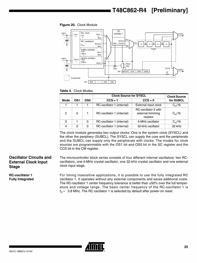
Clock Module The T48C862-R4 contains a clock module with 4 different internal oscillator types: twoRC-oscillators, one 4-MHz crystal oscillator and one 32-kHz crystal oscillator. The pinsOSC1 and OSC2 are the interface to connect a crystal either to the 4-MHz, or to the32-kHz crystal oscillator. OSC1 can be used as input for external clocks or to connect anexternal trimming resistor for the RC-oscillator 2. All necessary circuitry, except the crys-tal and the trimming resistor, is integrated on-chip. One of these oscillator types or anexternal input clock can be selected to generate the system clock (SYSCL).
In applications that do not require exact timing, it is possible to use the fully integratedRC-oscillator 1 without any external components. The RC-oscillator 1 center frequencytolerance is better than ± 50%. The RC-oscillator 2 is a trimmable oscillator whereby theoscillator frequency can be trimmed with an external resistor attached between OSC1and VDD. In this configuration, the RC-oscillator 2 frequency can be maintained stablewith a tolerance of ± 15% over the full operating temperature and voltage range.
The clock module is programmable via software with the clock management register(CM) and the system configuration register (SC). The required oscillator configurationcan be selected with the OS1 bit and the OS0 bit in the SC register. A programmable4-bit divider stage allows the adjustment of the system clock speed. A special feature ofthe clock management is that an external oscillator may be used and switched on andoff via a port pin for the power-down mode. Before the external clock is switched off, theinternal RC-oscillator 1 must be selected with the CCS bit and then the SLEEP modemay be activated. In this state an interrupt can wake up the controller with the RC-oscil-lator, and the external oscillator can be activated and selected by software. Asynchronization stage avoids too short clock periods if the clock source or the clockspeed is changed. If an external input clock is selected, a supervisor circuit monitors theexternal input and generates a hardware reset if the external clock source fails or dropsbelow 500 kHz for more than 1 ms.
VDD
Low thresholdMiddle thresholdHigh threshold
VMS = 1
Low thresholdMiddle thresholdHigh threshold
VMS = 0
3.0 V2.6 V2.2 V
1.3 V
VMI
VMS = 1
VMS = 0
Positive slope
Negative slope
VMS = 1
VMS = 0
Interrupt negative slope
Interrupt positive slope
Internal reference level
t
25
T48C862-R4 [Preliminary]
4551C–4BMCU–01/04
Figure 20. Clock Module
Table 4. Clock Modes
The clock module generates two output clocks. One is the system clock (SYSCL) andthe other the periphery (SUBCL). The SYSCL can supply the core and the peripheralsand the SUBCL can supply only the peripherals with clocks. The modes for clocksources are programmable with the OS1 bit and OS0 bit in the SC register and theCCS bit in the CM register.
Oscillator Circuits and External Clock Input Stage
The microcontroller block series consists of four different internal oscillators: two RC-oscillators, one 4-MHz crystal oscillator, one 32-kHz crystal oscillator and one externalclock input stage.
RC-oscillator 1 Fully Integrated
For timing insensitive applications, it is possible to use the fully integrated RCoscillator 1. It operates without any external components and saves additional costs.The RC-oscillator 1 center frequency tolerance is better than ±50% over the full temper-ature and voltage range. The basic center frequency of the RC-oscillator 1 isfO ≈ 3.8 MHz. The RC oscillator 1 is selected by default after power-on reset.
Mode OS1 OS0
Clock Source for SYSCL Clock Source for SUBCLCCS = 1 CCS = 0
1 1 1 RC-oscillator 1 (internal) External input clock Cin/16
2 0 1 RC-oscillator 1 (internal)RC-oscillator 2 with external trimming
resistorCin/16
3 1 0 RC-oscillator 1 (internal) 4-MHz oscillator Cin/16
4 0 0 RC-oscillator 1 (internal) 32-kHz oscillator 32 kHz
Ext. clockExIn
ExOut
Stop
RC oscillator2RCOut2
StopRTrim
4-MHz oscillator4OutStop
OscinOscout
Oscin
Oscout
32-kHz oscillator
32Out
OscinOscout
RCoscillator 1
RCOut1ControlStop
IN1
IN2
Cin/2 /2 /2 /2
Divider
SleepWDLOsc-
Stop
NSTOP CCS CSS1 CSS0CM:
BOT - - - OS1 OS0
SUBCL
SYSCL
SC:
*
OSC1
*
OSC2
*Configurable
Cin/16
32 kHz
26 T48C862-R4 [Preliminary] 4551C–4BMCU–01/04
Figure 21. RC-oscillator 1
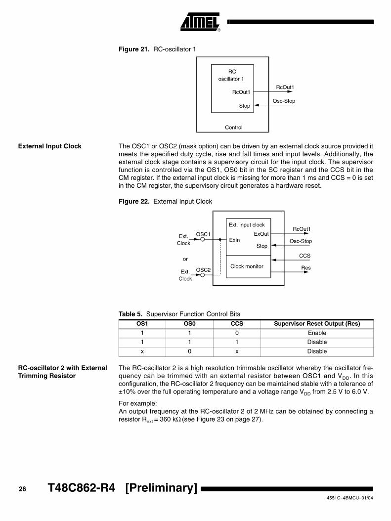
External Input Clock The OSC1 or OSC2 (mask option) can be driven by an external clock source provided itmeets the specified duty cycle, rise and fall times and input levels. Additionally, theexternal clock stage contains a supervisory circuit for the input clock. The supervisorfunction is controlled via the OS1, OS0 bit in the SC register and the CCS bit in theCM register. If the external input clock is missing for more than 1 ms and CCS = 0 is setin the CM register, the supervisory circuit generates a hardware reset.
Figure 22. External Input Clock
Table 5. Supervisor Function Control Bits
RC-oscillator 2 with External Trimming Resistor
The RC-oscillator 2 is a high resolution trimmable oscillator whereby the oscillator fre-quency can be trimmed with an external resistor between OSC1 and VDD. In thisconfiguration, the RC-oscillator 2 frequency can be maintained stable with a tolerance of±10% over the full operating temperature and a voltage range VDD from 2.5 V to 6.0 V.
For example: An output frequency at the RC-oscillator 2 of 2 MHz can be obtained by connecting aresistor Rext = 360 kΩ (see Figure 23 on page 27).
RCoscillator 1
RcOut1
Stop
Control
RcOut1
Osc-Stop
OS1 OS0 CCS Supervisor Reset Output (Res)
1 1 0 Enable
1 1 1 Disable
x 0 x Disable
Ext. input clock
ExOut
Stop
Ext.Clock
RcOut1
Osc-StopExIn
CCS
Res
OSC1
OSC2Clock monitor
Ext.Clock
or

27
T48C862-R4 [Preliminary]
4551C–4BMCU–01/04
Figure 23. RC-oscillator 2
4-MHz Oscillator The microcontroller block 4-MHz oscillator options need a crystal or ceramic resonatorconnected to the OSC1 and OSC2 pins to establish oscillation. All the necessary oscilla-tor circuitry is integrated, except the actual crystal, resonator, C3 and C4.
Figure 24. 4-MHz Crystal Oscillator
Figure 25. Ceramic Resonator
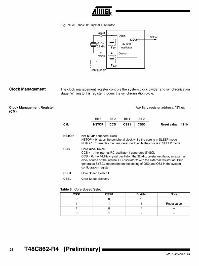
32-kHz Oscillator Some applications require long-term time keeping or low resolution timing. In this case,an on-chip, low power 32-kHz crystal oscillator can be used to generate both theSUBCL and the SYSCL. In this mode, power consumption is greatly reduced. The32-kHz crystal oscillator can not be stopped while the power-down mode is in operation.
RCoscillator 2
RcOut2
Stop
RcOut2
Osc-StopRTrim
OSC1
OSC2
Rext
VDD
4-MHzoscillator
4Out4Out
OSC1
OSC2
*Oscin
C1
*
C2
Oscout
XTAL4 MHz
*
Configurable
StopOsc-Stop
4-MHzoscillator
4Out
Stop
4Out
Osc-Stop
OSC1
OSC2
*Oscin
C1
*
C2
Oscout
Cer.Res
*
Configurable
C3
C4
28 T48C862-R4 [Preliminary] 4551C–4BMCU–01/04
Figure 26. 32-kHz Crystal Oscillator
Clock Management The clock management register controls the system clock divider and synchronizationstage. Writing to this register triggers the synchronization cycle.
Clock Management Register (CM)
Auxiliary register address: "3"hex
Table 6. Core Speed Select
32-kHzoscillator
32Out32Out
OSC1
OSC2
*
Oscin
C1
*
C2
Oscout
XTAL32 kHz
*
Configurable
Bit 3 Bit 2 Bit 1 Bit 0
CM: NSTOP CCS CSS1 CSS0 Reset value: 1111b
NSTOP Not STOP peripheral clockNSTOP = 0, stops the peripheral clock while the core is in SLEEP modeNSTOP = 1, enables the peripheral clock while the core is in SLEEP mode
CCS Core Clock SelectCCS = 1, the internal RC-oscillator 1 generates SYSCLCCS = 0, the 4-MHz crystal oscillator, the 32-kHz crystal oscillator, an external clock source or the internal RC-oscillator 2 with the external resistor at OSC1 generates SYSCL dependent on the setting of OS0 and OS1 in the system configuration register
CSS1 Core Speed Select 1
CSS0 Core Speed Select 0
CSS1 CSS0 Divider Note
0 0 16 –
1 1 8 Reset value
1 0 4 –
0 1 2 –
29
T48C862-R4 [Preliminary]
4551C–4BMCU–01/04
System Configuration Register (SC)
Primary register address: "3"hex
Table 7. Oscillator Select
Power-down Modes The sleep mode is a shut-down condition which is used to reduce the average systempower consumption in applications where the microcontroller is not fully utilized. In thismode, the system clock is stopped. The sleep mode is entered via the SLEEP instruc-tion. This instruction sets the interrupt enable bit (I) in the condition code register toenable all interrupts and stops the core. During the sleep mode the peripheral modulesremain active and are able to generate interrupts. The microcontroller exits the sleepmode by carrying out any interrupt or a reset.
The sleep mode can only be kept when none of the interrupt pending or active registerbits are set. The application of the $AUTOSLEEP routine ensures the correct function ofthe sleep mode. For standard applications use the $AUTOSLEEP routine to enter thepower-down mode. Using the SLEEP instruction instead of the $AUTOSLEEP followingan I/O instruction requires to insert 3 non-I/O instruction cycles (for example NOP NOPNOP) between the IN or OUT command and the SLEEP command.
The total power consumption is directly proportional to the active time of the microcon-troller. For a rough estimation of the expected average system current consumption, thefollowing formula should be used:
Itotal (VDD, fsyscl) = ISleep + (IDD × tactive/ttotal)
IDD depends on VDD and fsyscl
Bit 3 Bit 2 Bit 1 Bit 0
SC: write BOT – OS1 OS0 Reset value: 1x11b
BOT Brown-Out ThresholdBOT = 1, low brown-out voltage threshold (1.7 V)BOT = 0, high brown-out voltage threshold (2.0 V)
OS1 Oscillator Select 1
OS0 Oscillator Select 0
Mode OS1 OS0 Input for SUBCL Selected Oscillators
1 1 1 Cin/16 RC-oscillator 1 and external input clock
2 0 1 Cin/16 RC-oscillator 1 and RC-oscillator 2
3 1 0 Cin/16 RC-oscillator 1 and 4-MHz crystal oscillator
4 0 0 32 kHzRC-oscillator 1 and 32-kHz crystal oscillator
Note: If bit CCS = 0 in the CM register the RC-oscillator 1 always stops.
30 T48C862-R4 [Preliminary] 4551C–4BMCU–01/04
The microcontroller block has various power-down modes. During the sleep mode theclock for the microcontroller block core is stopped. With the NSTOP bit in the clock man-agement register (CM), it is programmable if the clock for the on-chip peripherals isactive or stopped during the sleep mode. If the clock for the core and the peripherals isstopped, the selected oscillator is switched off. An exception is the 32-kHz oscillator, if itis selected it runs continuously independent of the NSTOP bit. If the oscillator is stoppedor the 32-kHz oscillator is selected, power consumption is extremely low.
Table 8. Power-down Modes
Peripheral Modules
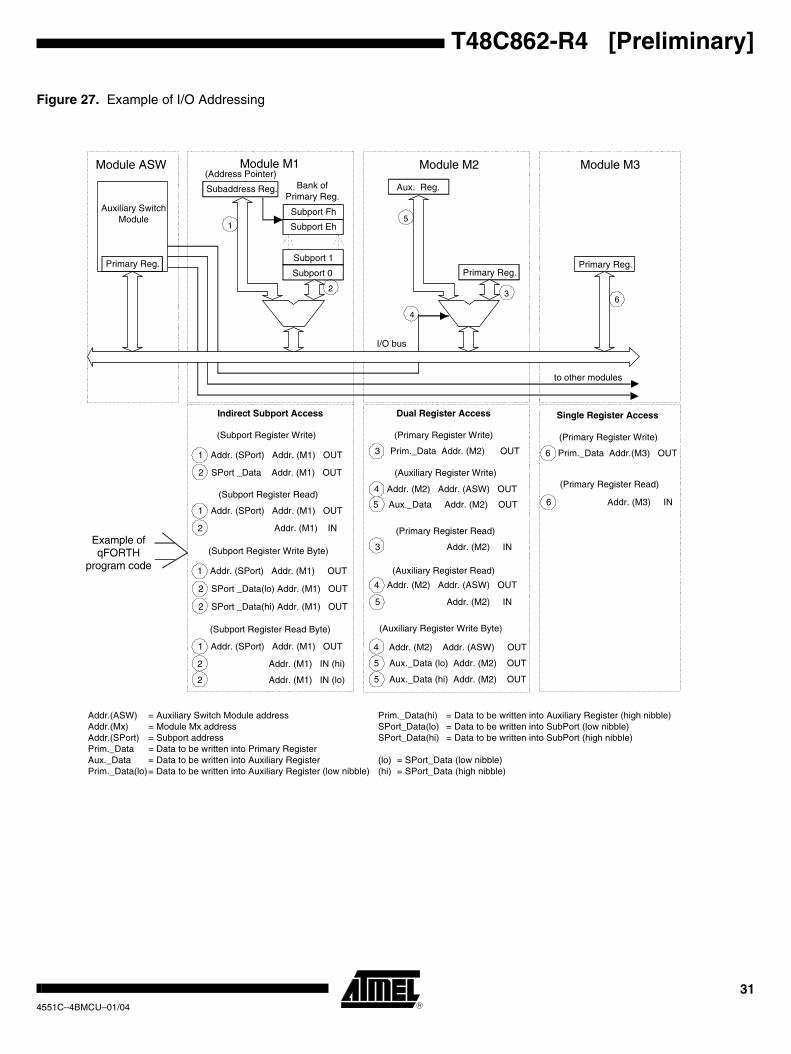
Addressing Peripherals Accessing the peripheral modules takes place via the I/O bus (see Figure 27 on page31). The IN or OUT instructions allow direct addressing of up to 16 I/O modules. A dualregister addressing scheme has been adopted to enable direct addressing of the pri-mary register. To address the auxiliary register, the access must be switched with anauxiliary switching module. Thus, a single IN (or OUT) to the module address will read(or write into) the module primary register. Accessing the auxiliary register is performedwith the same instruction preceded by writing the module address into the auxiliaryswitching module. Byte wide registers are accessed by multiple IN- (or OUT-) instruc-tions. For more complex peripheral modules, with a larger number of registers,extended addressing is used. In this case, a bank of up to 16 subport registers are indi-rectly addressed with the subport address. The first OUT instruction writes the subportaddress to the sub address register, the second IN or OUT instruction reads data fromor writes data to the addressed subport.
ModeCPU Core
Osc-Stop(1)
Brown-out
Function
RC-oscillator 1RC-oscillator 2
4-MHz Oscillator
32-kHz Oscillator
External Input Clock
Active RUN NO Active RUN RUN YES
Power-down
SLEEP NO Active RUN RUN YES
SLEEP SLEEP YES STOP STOP RUN STOP
Note: 1. Osc-Stop = SLEEP and NSTOP and WDL
31
T48C862-R4 [Preliminary]
4551C–4BMCU–01/04
Figure 27. Example of I/O Addressing
1
23
4
5
Module ASW Module M1 Module M2 Module M3
Auxiliary SwitchModule
Primary Reg.
(Address Pointer)
Subaddress Reg. Bank ofPrimary Reg.
to other modules
Subport Fh
Subport Eh
Subport 1
Subport 0Primary Reg.
Aux. Reg.
Primary Reg.
I/O bus
Example ofqFORTH
program code
Indirect Subport Access
(Subport Register Write)
1 Addr. (SPort) Addr. (M1) OUT
2 SPort _Data Addr. (M1) OUT
(Subport Register Read)
1 Addr. (SPort) Addr. (M1) OUT
2 Addr. (M1) IN
(Subport Register Write Byte)
1 Addr. (SPort) Addr. (M1) OUT
(Subport Register Read Byte)
1 Addr. (SPort) Addr. (M1) OUT
2 Addr. (M1) IN (hi)
2 Addr. (M1) IN (lo)
3 Prim._Data Addr. (M2) OUT
4 Addr. (M2) Addr. (ASW) OUT
4 Addr. (M2) Addr. (ASW) OUT
Dual Register Access
(Primary Register Write)
(Auxiliary Register Write)
5 Aux._Data Addr. (M2) OUT
(Primary Register Read)
5 Addr. (M2) IN
(Auxiliary Register Read)
3 Addr. (M2) IN
(Auxiliary Register Write Byte)
4 Addr. (M2) Addr. (ASW) OUT
5 Aux._Data (lo) Addr. (M2) OUT
5 Aux._Data (hi) Addr. (M2) OUT
6 Prim._Data Addr.(M3) OUT
Single Register Access
(Primary Register Write)
6 Addr. (M3) IN
(Primary Register Read)
2 SPort _Data(lo) Addr. (M1) OUT
2 SPort _Data(hi) Addr. (M1) OUT
6
Addr.(ASW) = Auxiliary Switch Module addressAddr.(Mx) = Module Mx addressAddr.(SPort) = Subport addressPrim._Data = Data to be written into Primary RegisterAux._Data = Data to be written into Auxiliary RegisterPrim._Data(lo)= Data to be written into Auxiliary Register (low nibble)
Prim._Data(hi) = Data to be written into Auxiliary Register (high nibble)SPort_Data(lo) = Data to be written into SubPort (low nibble)SPort_Data(hi) = Data to be written into SubPort (high nibble)
(lo) = SPort_Data (low nibble)(hi) = SPort_Data (high nibble)

32 T48C862-R4 [Preliminary] 4551C–4BMCU–01/04
Table 9. Peripheral Addresses
Port Address NameWrite/ Read Reset Value Register Function
ModuleType
1 P1DAT W/R 1xx1b Port 1 - data register/input data M3
2 P2DAT W/R 1111b Port 2 - data register/pin data M2
Auxiliary P2CR W 1111b Port 2 - control register
3 SC W 1x11b System configuration register M3
CWD R xxxxb Watchdog reset M3
Auxiliary CM W 1111b Clock management register M2
4 P4DAT W/R 1111b Port 4 - data register/pin data M2
Auxiliary P4CR W 1111 1111b Port 4 - control register (byte)
5 P5DAT W/R 1111b Port 5 - data register/pin data M2
Auxiliary P5CR W 1111 1111b Port 5 - control register (byte)
6 P6DAT W/R 1xx1b Port 6 - data register/pin data M2
Auxiliary P6CR W 1111b Port 6 - control register (byte)
7 T12SUB W – Data to Timer 1/2 subport M1
Subport address
0 T2C W 0000b Timer 2 control register M1
1 T2M1 W 1111b Timer 2 mode register 1 M1
2 T2M2 W 1111b Timer 2 mode register 2 M1
3 T2CM W 0000b Timer 2 compare mode register M1
4 T2CO1 W 1111b Timer 2 compare register 1 M1
5 T2CO2 W 1111 1111b Timer 2 compare register 2 (byte) M1
6 – – – Reserved
7 – – – Reserved
8 T1C1 W 1111b Timer 1 control register 1 M1
9 T1C2 W x111b Timer 1 control register 2 M1
A WDC W 1111b Watchdog control register M1
B-F Reserved
8 ASW W 1111b Auxiliary/switch register ASW
9 STB W xxxx xxxxb Serial transmit buffer (byte) M2
SRB R xxxx xxxxb Serial receive buffer (byte)
Auxiliary SIC1 W 1111b Serial interface control register 1
A SISC W/R 1x11b Serial interface status/control register M2
Auxiliary SIC2 W 1111b Serial interface control register 2
B T3SUB W/R – Data to/from Timer 3 subport M1
Subport address
0 T3M W 1111b Timer 3 mode register M1
1 T3CS W 1111b Timer 3 clock select register M1
2 T3CM1 W 0000b Timer 3 compare mode register 1 M1
3 T3CM2 W 0000b Timer 3 compare mode register 2 M1
4 T3CO1 W 1111 1111b Timer 3 compare register 1 (byte) M1
4 T3CP R xxxx xxxxb Timer 3 capture register (byte) M1
5 T3CO2 W 1111 1111b Timer 3 compare register 2 (byte) M1
6 W 1111b Reserved
7-F – Reserved
C T3C W 0000b Timer 3 control register M3
T3ST R x000b Timer 3 status register M3
D, E – – Reserved
F VMC W 1111b Voltage monitor control register M3
VMST R xx11b Voltage monitor status register M3
33
T48C862-R4 [Preliminary]
4551C–4BMCU–01/04
Bi-directional Ports With the exception of Port 1 and Port 6, all other ports (2, 4 and 5) are 4 bits wide. Port 1and Port 6 have a data width of 2 bits (bit 0 and bit 3). All ports may be used for datainput or output. All ports are equipped with Schmitt trigger inputs and a variety of maskoptions for open-drain, open-source, full-complementary outputs, pull-up and pull-downtransistors. All Port Data Registers (PxDAT) are I/O mapped to the primary address reg-ister of the respective port address and the Port Control Register (PxCR), to thecorresponding auxiliary register.
There are five different directional ports available:
Port 1 2-bit wide bi-directional port with automatic full bus width direction switching.
Port 2 4-bit wide bitwise-programmable I/O port.
Port 5 4-bit wide bitwise-programmable bi-directional port with optional strong pull-ups and programmable interrupt logic.
Port 4 4-bit wide bitwise-programmable bi-directional port also provides the I/Ointerface to Timer 2, SSI, voltage monitor input and external interrupt input.
Port 6 2-bit wide bitwise-programmable bi-directional port also provides the I/O interface to Timer 3 and external interrupt input.
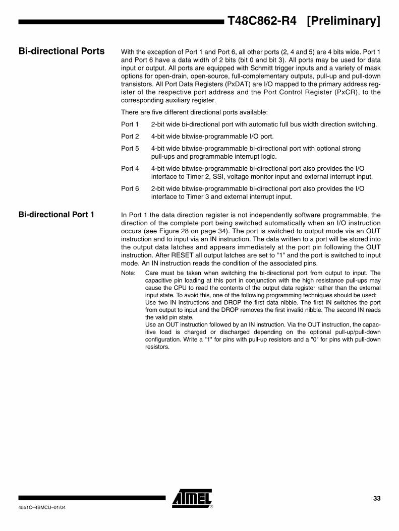
Bi-directional Port 1 In Port 1 the data direction register is not independently software programmable, thedirection of the complete port being switched automatically when an I/O instructionoccurs (see Figure 28 on page 34). The port is switched to output mode via an OUTinstruction and to input via an IN instruction. The data written to a port will be stored intothe output data latches and appears immediately at the port pin following the OUTinstruction. After RESET all output latches are set to "1" and the port is switched to inputmode. An IN instruction reads the condition of the associated pins.Note: Care must be taken when switching the bi-directional port from output to input. The
capacitive pin loading at this port in conjunction with the high resistance pull-ups maycause the CPU to read the contents of the output data register rather than the externalinput state. To avoid this, one of the following programming techniques should be used:Use two IN instructions and DROP the first data nibble. The first IN switches the portfrom output to input and the DROP removes the first invalid nibble. The second IN readsthe valid pin state. Use an OUT instruction followed by an IN instruction. Via the OUT instruction, the capac-itive load is charged or discharged depending on the optional pull-up/pull-downconfiguration. Write a "1" for pins with pull-up resistors and a "0" for pins with pull-downresistors.
34 T48C862-R4 [Preliminary] 4551C–4BMCU–01/04
Figure 28. Bi-directional Port 1
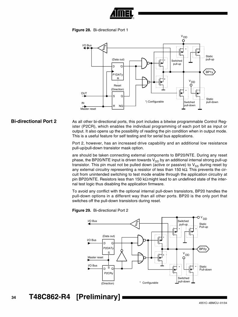
Bi-directional Port 2 As all other bi-directional ports, this port includes a bitwise programmable Control Reg-ister (P2CR), which enables the individual programming of each port bit as input oroutput. It also opens up the possibility of reading the pin condition when in output mode.This is a useful feature for self testing and for serial bus applications.
Port 2, however, has an increased drive capability and an additional low resistancepull-up/pull-down transistor mask option.
are should be taken connecting external components to BP20/NTE. During any resetphase, the BP20/NTE input is driven towards VDD by an additional internal strong pull-uptransistor. This pin must not be pulled down (active or passive) to VSS during reset byany external circuitry representing a resistor of less than 150 kΩ. This prevents the cir-cuit from unintended switching to test mode enable through the application circuitry atpin BP20/NTE. Resistors less than 150 kΩ might lead to an undefined state of the inter-nal test logic thus disabling the application firmware.
To avoid any conflict with the optional internal pull-down transistors, BP20 handles thepull-down options in a different way than all other ports. BP20 is the only port thatswitches off the pull-down transistors during reset.
Figure 29. Bi-directional Port 2
OUT
IN
Reset
I/O Bus
D
R
S
Q
Q
NQ
R
Master reset
P1DATy
(Data out)
(Direction)
BP1y
V DD
*
Switched pull-up
*
**
*
*) Configurable
V DD
Staticpull-up
Staticpull-downSwitched
pull-down
Master reset
Q
Q
BP2y
Configurable
*
*
P2DATy
P2CRy
I/O Bus
D
I/O Bus
I/O Bus
*
*
Switched pull-up
*
StaticPull-up
(Data out)
(Direction) *
SD
*S
*
VDD
StaticPull-down
Switched pull-down
VDD
35
T48C862-R4 [Preliminary]
4551C–4BMCU–01/04
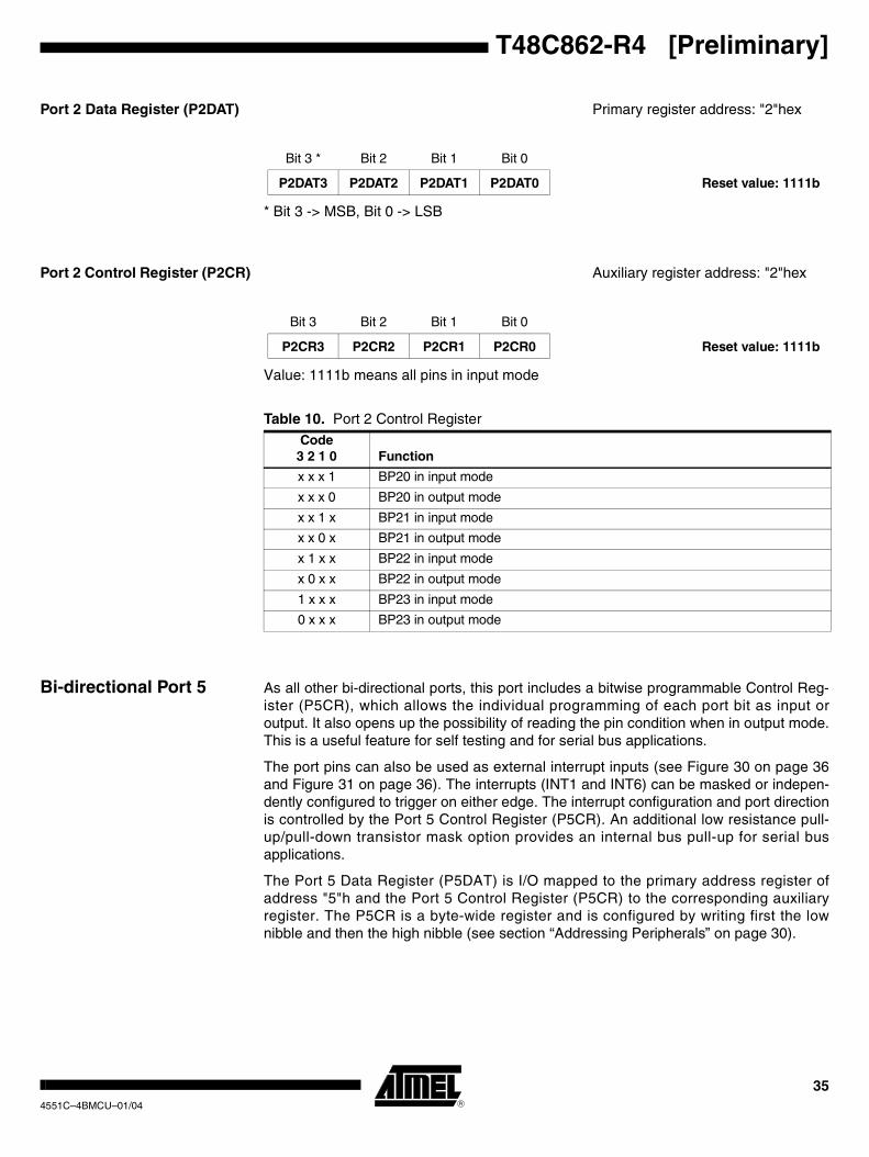
Port 2 Data Register (P2DAT) Primary register address: "2"hex
* Bit 3 -> MSB, Bit 0 -> LSB
Port 2 Control Register (P2CR) Auxiliary register address: "2"hex
Value: 1111b means all pins in input mode
Table 10. Port 2 Control Register
Bi-directional Port 5 As all other bi-directional ports, this port includes a bitwise programmable Control Reg-ister (P5CR), which allows the individual programming of each port bit as input oroutput. It also opens up the possibility of reading the pin condition when in output mode.This is a useful feature for self testing and for serial bus applications.
The port pins can also be used as external interrupt inputs (see Figure 30 on page 36and Figure 31 on page 36). The interrupts (INT1 and INT6) can be masked or indepen-dently configured to trigger on either edge. The interrupt configuration and port directionis controlled by the Port 5 Control Register (P5CR). An additional low resistance pull-up/pull-down transistor mask option provides an internal bus pull-up for serial busapplications.
The Port 5 Data Register (P5DAT) is I/O mapped to the primary address register ofaddress "5"h and the Port 5 Control Register (P5CR) to the corresponding auxiliaryregister. The P5CR is a byte-wide register and is configured by writing first the lownibble and then the high nibble (see section “Addressing Peripherals” on page 30).
Bit 3 * Bit 2 Bit 1 Bit 0
P2DAT3 P2DAT2 P2DAT1 P2DAT0 Reset value: 1111b
Bit 3 Bit 2 Bit 1 Bit 0
P2CR3 P2CR2 P2CR1 P2CR0 Reset value: 1111b
Code 3 2 1 0 Function
x x x 1 BP20 in input mode
x x x 0 BP20 in output mode
x x 1 x BP21 in input mode
x x 0 x BP21 in output mode
x 1 x x BP22 in input mode
x 0 x x BP22 in output mode
1 x x x BP23 in input mode
0 x x x BP23 in output mode
36 T48C862-R4 [Preliminary] 4551C–4BMCU–01/04
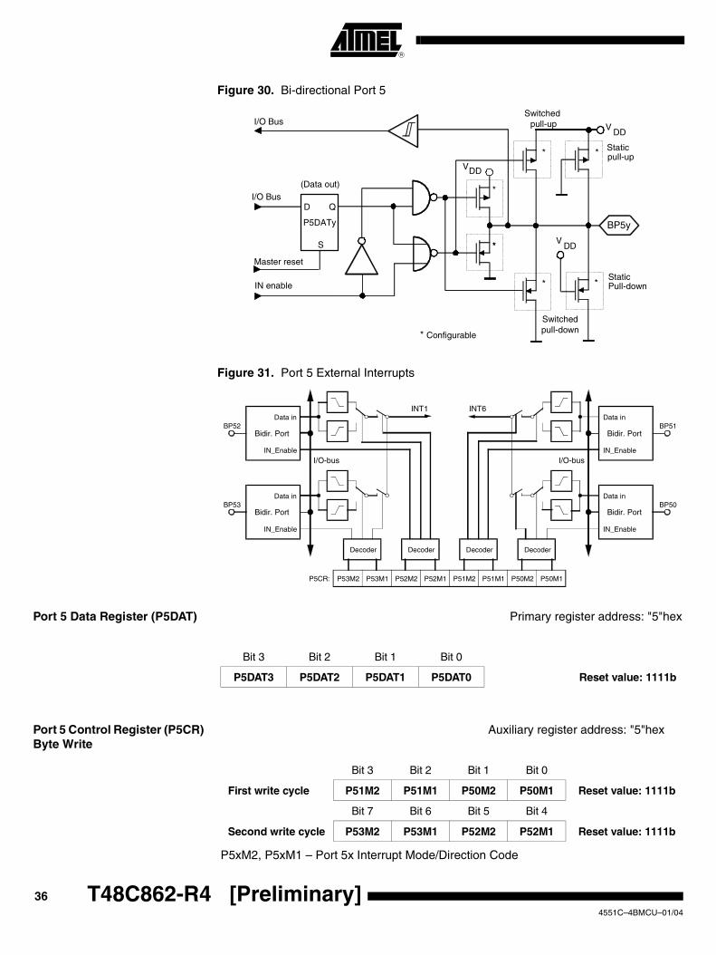
Figure 30. Bi-directional Port 5
Figure 31. Port 5 External Interrupts
Port 5 Data Register (P5DAT) Primary register address: "5"hex
Port 5 Control Register (P5CR) Byte Write
Auxiliary register address: "5"hex
P5xM2, P5xM1 – Port 5x Interrupt Mode/Direction Code
Master reset
Q
VDD
BP5y
Configurable
*
*
P5DATy
I/O Bus
D
IN enable
I/O Bus
*
*
Switched pull-up
Switchedpull-down
* Staticpull-up
(Data out)
*
*S
*
VDD
StaticPull-down
VDD
Bidir. Port
Data in
IN_Enable
BP53
P53M2 P53M1 P52M2 P52M1 P51M2 P51M1 P50M2 P50M1
Decoder Decoder Decoder Decoder
Bidir. Port
Data in
IN_Enable
BP52
I/O-bus
Bidir. Port
Data in
IN_Enable
BP51
I/O-bus
Bidir. Port
Data in
IN_Enable
BP50
INT1 INT6
P5CR:
Bit 3 Bit 2 Bit 1 Bit 0
P5DAT3 P5DAT2 P5DAT1 P5DAT0 Reset value: 1111b
Bit 3 Bit 2 Bit 1 Bit 0
First write cycle P51M2 P51M1 P50M2 P50M1 Reset value: 1111b
Bit 7 Bit 6 Bit 5 Bit 4
Second write cycle P53M2 P53M1 P52M2 P52M1 Reset value: 1111b
37
T48C862-R4 [Preliminary]
4551C–4BMCU–01/04
Table 11. Port 5 Control Register
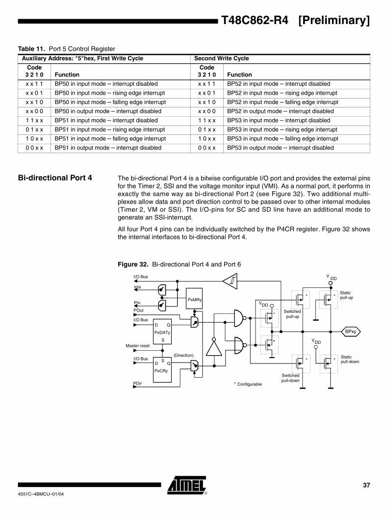
Bi-directional Port 4 The bi-directional Port 4 is a bitwise configurable I/O port and provides the external pinsfor the Timer 2, SSI and the voltage monitor input (VMI). As a normal port, it performs inexactly the same way as bi-directional Port 2 (see Figure 32). Two additional multi-plexes allow data and port direction control to be passed over to other internal modules(Timer 2, VM or SSI). The I/O-pins for SC and SD line have an additional mode togenerate an SSI-interrupt.
All four Port 4 pins can be individually switched by the P4CR register. Figure 32 showsthe internal interfaces to bi-directional Port 4.
Figure 32. Bi-directional Port 4 and Port 6
Auxiliary Address: "5"hex, First Write Cycle Second Write Cycle
Code3 2 1 0 Function
Code3 2 1 0 Function
x x 1 1 BP50 in input mode – interrupt disabled x x 1 1 BP52 in input mode – interrupt disabled
x x 0 1 BP50 in input mode – rising edge interrupt x x 0 1 BP52 in input mode – rising edge interrupt
x x 1 0 BP50 in input mode – falling edge interrupt x x 1 0 BP52 in input mode – falling edge interrupt
x x 0 0 BP50 in output mode – interrupt disabled x x 0 0 BP52 in output mode – interrupt disabled
1 1 x x BP51 in input mode – interrupt disabled 1 1 x x BP53 in input mode – interrupt disabled
0 1 x x BP51 in input mode – rising edge interrupt 0 1 x x BP53 in input mode – rising edge interrupt
1 0 x x BP51 in input mode – falling edge interrupt 1 0 x x BP53 in input mode – falling edge interrupt
0 0 x x BP51 in output mode – interrupt disabled 0 0 x x BP53 in output mode – interrupt disabled
Master reset
Q
VDD
VDD
BPxy
Configurable
*
*
PxDATy
I/O Bus
D
I/O Bus
I/O Bus
*
*Switched
pull-up
Switchedpull-down
*
*S
PxCRy
SQD
PxMRy
POut
(Direction)
PDir
Intx
*
*PIn
VDD
Staticpull-up
Staticpull-down

38 T48C862-R4 [Preliminary] 4551C–4BMCU–01/04
Port 4 Data Register (P4DAT) Primary register address: "4"hex
Port 4 Control Register (P4CR) Byte Write
Auxiliary register address: "4"hex
P4xM2, P4xM1 – Port 4x Interrupt mode/direction code
Table 12. Port 4 Control Register
Bi-directional Port 6 The bi-directional Port 6 is a bitwise configurable I/O port and provides the external pinsfor the Timer 3. As a normal port, it performs in exactly the same way as bi-directionalPort 6 (see Figure 32 on page 37). Two additional multiplexes allow data and port direc-tion control to be passed over to other internal module (Timer 3). The I/O pin for T3I linehas an additional mode to generate a Timer 3 interrupt.
All two Port 6 pins can be individually switched by the P6CR register. Figure 32 on page37 shows the internal interfaces to bi-directional Port 6.
Bit 3 Bit 2 Bit 1 Bit 0
P4DAT3 P4DAT2 P4DAT1 P4DAT0 Reset value: 1111b
Bit 3 Bit 2 Bit 1 Bit 0
First write cycle P41M2 P41M1 P40M2 P40M1 Reset value: 1111b
Bit 7 Bit 6 Bit 5 Bit 4
Second write cycle P43M2 P43M1 P42M2 P42M1 Reset value: 1111b
Auxiliary Address: "4"hexFirst Write Cycle Second Write Cycle
Code3 2 1 0 Function
Code3 2 1 0 Function
x x 1 1 BP40 in input mode x x 1 1 BP42 in input mode
x x 1 0 BP40 in output mode x x 1 0 BP42 in output mode
x x 0 1BP40 enable alternate function (SC for SSI)
x x 0 xBP42 enable alternate function (T2O for Timer 2)
x x 0 0BP40 enable alternate function (falling edge interrupt input for INT3)
1 1 x x BP43 in input mode
1 1 x x BP41 in input mode 1 0 x x BP43 in output mode
1 0 x x BP41 in output mode 0 1 x xBP43 enable alternate function (SD for SSI)
0 1 x xBP41 enable alternate function (VMI for voltage monitor input)
0 0 x xBP43 enable alternate function (falling edge interrupt input for INT3)
0 0 x xBP41 enable alternate function (T2I external clock input for Timer 2)
– –

39
T48C862-R4 [Preliminary]
4551C–4BMCU–01/04
Port 6 Data Register (P6DAT) Primary register address: "6"hex
Port 6 Control Register (P6CR) Auxiliary register address: "6"hex
P6xM2, P6xM1 – Port 6x Interrupt mode/direction code
Table 13. Port 6 Control Register
Universal Timer/Counter/ Communication Module (UTCM)
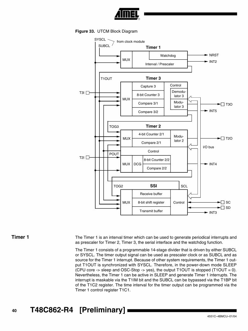
The Universal Timer/counter/Communication Module (UTCM) consists of three timers(Timer 1,Timer 2, Timer 3) and a Synchronous Serial Interface (SSI).
• Timer 1 is an interval timer that can be used to generate periodical interrupts and as prescaler for Timer 2, Timer 3, the serial interface and the watchdog function.
• Timer 2 is an 8/12-bit timer with an external clock input (T2I) and an output (T2O).
• Timer 3 is an 8-bit timer/counter with its own input (T3I) and output (T3O).
• The SSI operates as two wire serial interface or as shift register for modulation and demodulation. The modulator and demodulator units work together with the timers and shift the data bits into or out of the shift register.
There is a multitude of modes in which the timers and the serial interface can worktogether.
Bit 3 Bit 2 Bit 1 Bit 0
P6DAT3 – – P6DAT0 Reset value: 1xx1b
Bit 3 Bit 2 Bit 1 Bit 0
P63M2 P63M1 P60M2 P60M0 Reset value: 1111b
Auxiliary Address: "6"hex Write Cycle
Code3 2 1 0 Function
Code3 2 1 0 Function
x x 1 1 BP60 in input mode 1 1 x x BP63 in input mode
x x 1 0 BP60 in output mode 1 0 x x BP63 in output mode
x x 0 xBP60 enable alternate port function (T3O for Timer 3)
0 x x xBP63 enable alternate port function (T3I for Timer 3)
40 T48C862-R4 [Preliminary] 4551C–4BMCU–01/04
Figure 33. UTCM Block Diagram
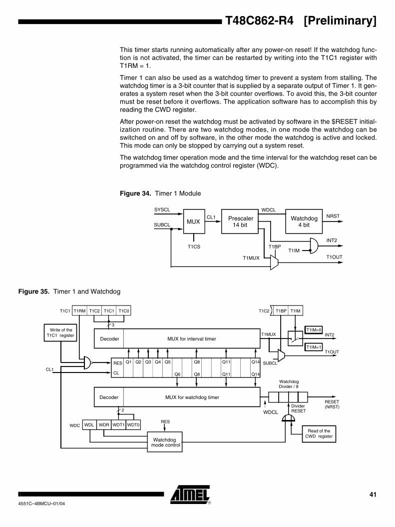
Timer 1 The Timer 1 is an interval timer which can be used to generate periodical interrupts andas prescaler for Timer 2, Timer 3, the serial interface and the watchdog function.
The Timer 1 consists of a programmable 14-stage divider that is driven by either SUBCLor SYSCL. The timer output signal can be used as prescaler clock or as SUBCL and assource for the Timer 1 interrupt. Because of other system requirements, the Timer 1 out-put T1OUT is synchronized with SYSCL. Therefore, in the power-down mode SLEEP(CPU core -> sleep and OSC-Stop -> yes), the output T1OUT is stopped (T1OUT = 0).Nevertheless, the Timer 1 can be active in SLEEP and generate Timer 1 interrupts. Theinterrupt is maskable via the T1IM bit and the SUBCL can be bypassed via the T1BP bitof the T1C2 register. The time interval for the timer output can be programmed via theTimer 1 control register T1C1.
Demodu-lator 38-bit Counter 3
Capture 3
Compare 3/1
Compare 3/2
Modu-lator 3
MUX
MUX
Control
Watchdog
Interval / Prescaler
Timer 1
Timer 3
Modu-lator 2
4-bit Counter 2/1
Compare 2/1MUX
MUX DCG8-bit Counter 2/2
Compare 2/2
Control
Timer 2
MUX 8-bit shift register
Receive buffer
Transmit buffer
Control
SSI SCL
INT4
INT5
INT2
NRST
INT3
POUT
TOG2
TOG3
T1OUT
SUBCL
SYSCLfrom clock module
T3O
T3I
T2I
T2O
SC
SD
I/O bus
41
T48C862-R4 [Preliminary]
4551C–4BMCU–01/04
This timer starts running automatically after any power-on reset! If the watchdog func-tion is not activated, the timer can be restarted by writing into the T1C1 register withT1RM = 1.
Timer 1 can also be used as a watchdog timer to prevent a system from stalling. Thewatchdog timer is a 3-bit counter that is supplied by a separate output of Timer 1. It gen-erates a system reset when the 3-bit counter overflows. To avoid this, the 3-bit countermust be reset before it overflows. The application software has to accomplish this byreading the CWD register.
After power-on reset the watchdog must be activated by software in the $RESET initial-ization routine. There are two watchdog modes, in one mode the watchdog can beswitched on and off by software, in the other mode the watchdog is active and locked.This mode can only be stopped by carrying out a system reset.
The watchdog timer operation mode and the time interval for the watchdog reset can beprogrammed via the watchdog control register (WDC).
Figure 34. Timer 1 Module
Figure 35. Timer 1 and Watchdog
Prescaler14 bit
CL1 Watchdog4 bitMUX
WDCL
T1IMT1BP
T1MUX
NRST
INT2
T1OUT
T1CS
SYSCL
SUBCL
Q5Q1 Q2 Q3 Q4
Q6
Q8
Q8
Q11
Q11
Q14
Q14
RES
CL
Decoder
Watchdogmode control
MUX for interval timer
Decoder MUX for watchdog timer
T1RM T1C2 T1C1 T1C0
3
2
WDL WDR WDT1 WDT0WDCRES
T1MUX
SUBCL
T1BP T1IM
T1IM=0
T1IM=1
INT2
T1OUT
T1C2
RESET(NRST)
WatchdogDivider / 8
DividerRESET
T1C1
Write of theT1C1 register
CL1
WDCL
Read of theCWD register

42 T48C862-R4 [Preliminary] 4551C–4BMCU–01/04
Timer 1 Control Register 1 (T1C1)
Address: "7"hex - Subaddress: "8"hex
* Bit 3 -> MSB, Bit 0 -> LSB
The three bits T1C[2:0] select the divider for Timer 1. The resulting time intervaldepends on this divider and the Timer 1 input clock source. The timer input can be sup-plied by the system clock, the 32-kHz oscillator or via the clock management. If the clockmanagement generates the SUBCL, the selected input clock from the RC oscillator, 4-MHz oscillator or an external clock is divided by 16.
Table 14. Timer 1 Control Bits
Bit 3 * Bit 2 Bit 1 Bit 0
T1RM T1C2 T1C1 T1C0 Reset value: 1111b
T1RM Timer 1 Restart Mode T1RM = 0, write access without Timer 1 restartT1RM = 1, write access with Timer 1 restart
Note: If WDL = 0, Timer 1 restart is impossible
T1C2 Timer 1 Control bit 2
T1C1 Timer 1 Control bit 1
T1C0 Timer 1 Control bit 0
T1C2 T1C1 T1C0 DividerTime Interval with
SUBCLTime Interval withSUBCL = 32 kHz
Time Interval with SYSCL = 2/1 MHz
0 0 0 2 SUBCL/2 61 µs 1 µs/2 µs
0 0 1 4 SUBCL/4 122 µs 2 µs/4 µs
0 1 0 8 SUBCL/8 244 µs 4 µs/8 µs
0 1 1 16 SUBCL/16 488 µs 8 µs/16 µs
1 0 0 32 SUBCL/32 0.977 ms 16 µs/32 µs
1 0 1 256 SUBCL/256 7.812 ms 128 µs/256 µs
1 1 0 2048 SUBCL/2048 62.5 ms 1024 µs/2048 µs
1 1 1 16384 SUBCL/16384 500 ms 8192 µs/16384 µs
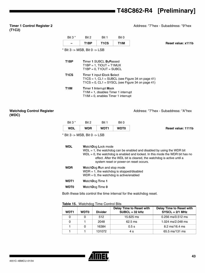
43
T48C862-R4 [Preliminary]
4551C–4BMCU–01/04
Timer 1 Control Register 2 (T1C2)
Address: "7"hex - Subaddress: "9"hex
* Bit 3 -> MSB, Bit 0 -> LSB
Watchdog Control Register (WDC)
Address: "7"hex - Subaddress: "A"hex
* Bit 3 -> MSB, Bit 0 -> LSB
Both these bits control the time interval for the watchdog reset.
Table 15. Watchdog Time Control Bits
Bit 3 * Bit 2 Bit 1 Bit 0
– T1BP T1CS T1IM Reset value: x111b
T1BP Timer 1 SUBCL ByPassedT1BP = 1, TIOUT = T1MUXT1BP = 0, T1OUT = SUBCL
T1CS Timer 1 input Clock SelectT1CS = 1, CL1 = SUBCL (see Figure 34 on page 41)T1CS = 0, CL1 = SYSCL (see Figure 34 on page 41)
T1IM Timer 1 Interrupt MaskT1IM = 1, disables Timer 1 interruptT1IM = 0, enables Timer 1 interrupt
Bit 3 * Bit 2 Bit 1 Bit 0
WDL WDR WDT1 WDT0 Reset value: 1111b
WDL WatchDog Lock mode WDL = 1, the watchdog can be enabled and disabled by using the WDR bitWDL = 0, the watchdog is enabled and locked. In this mode the WDR bit has no
effect. After the WDL bit is cleared, the watchdog is active until asystem reset or power-on reset occurs.
WDR WatchDog Run and stop modeWDR = 1, the watchdog is stopped/disabledWDR = 0, the watchdog is active/enabled
WDT1 WatchDog Time 1
WDT0 WatchDog Time 0
WDT1 WDT0 DividerDelay Time to Reset with
SUBCL = 32 kHzDelay Time to Reset with
SYSCL = 2/1 MHz
0 0 512 15.625 ms 0.256 ms/0.512 ms
0 1 2048 62.5 ms 1.024 ms/2.048 ms
1 0 16384 0.5 s 8.2 ms/16.4 ms
1 1 131072 4 s 65.5 ms/131 ms
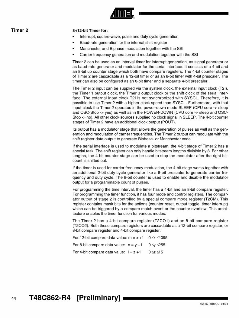
44 T48C862-R4 [Preliminary] 4551C–4BMCU–01/04
Timer 2 8-/12-bit Timer for:
• Interrupt, square-wave, pulse and duty cycle generation
• Baud-rate generation for the internal shift register
• Manchester and Biphase modulation together with the SSI
• Carrier frequency generation and modulation together with the SSI
Timer 2 can be used as an interval timer for interrupt generation, as signal generator oras baud-rate generator and modulator for the serial interface. It consists of a 4-bit andan 8-bit up counter stage which both have compare registers. The 4-bit counter stagesof Timer 2 are cascadable as a 12-bit timer or as an 8-bit timer with 4-bit prescaler. Thetimer can also be configured as an 8-bit timer and a separate 4-bit prescaler.
The Timer 2 input can be supplied via the system clock, the external input clock (T2I),the Timer 1 output clock, the Timer 3 output clock or the shift clock of the serial inter-face. The external input clock T2I is not synchronized with SYSCL. Therefore, it ispossible to use Timer 2 with a higher clock speed than SYSCL. Furthermore, with thatinput clock the Timer 2 operates in the power-down mode SLEEP (CPU core -> sleepand OSC-Stop -> yes) as well as in the POWER-DOWN (CPU core -> sleep and OSC-Stop -> no). All other clock sources supplied no clock signal in SLEEP. The 4-bit counterstages of Timer 2 have an additional clock output (POUT).
Its output has a modulator stage that allows the generation of pulses as well as the gen-eration and modulation of carrier frequencies. The Timer 2 output can modulate with theshift register data output to generate Biphase- or Manchester code.
If the serial interface is used to modulate a bitstream, the 4-bit stage of Timer 2 has aspecial task. The shift register can only handle bitstream lengths divisible by 8. For otherlengths, the 4-bit counter stage can be used to stop the modulator after the right bit-count is shifted out.
If the timer is used for carrier frequency modulation, the 4-bit stage works together withan additional 2-bit duty cycle generator like a 6-bit prescaler to generate carrier fre-quency and duty cycle. The 8-bit counter is used to enable and disable the modulatoroutput for a programmable count of pulses.
For programming the time interval, the timer has a 4-bit and an 8-bit compare register.For programming the timer function, it has four mode and control registers. The compar-ator output of stage 2 is controlled by a special compare mode register (T2CM). Thisregister contains mask bits for the actions (counter reset, output toggle, timer interrupt)which can be triggered by a compare match event or the counter overflow. This archi-tecture enables the timer function for various modes.
The Timer 2 has a 4-bit compare register (T2CO1) and an 8-bit compare register(T2CO2). Both these compare registers are cascadable as a 12-bit compare register, or8-bit compare register and 4-bit compare register.
For 12-bit compare data value: m = x +1 0 ≤ x ≤ 4095
For 8-bit compare data value: n = y +1 0 ≤ y ≤ 255
For 4-bit compare data value: l = z +1 0 ≤ z ≤ 15
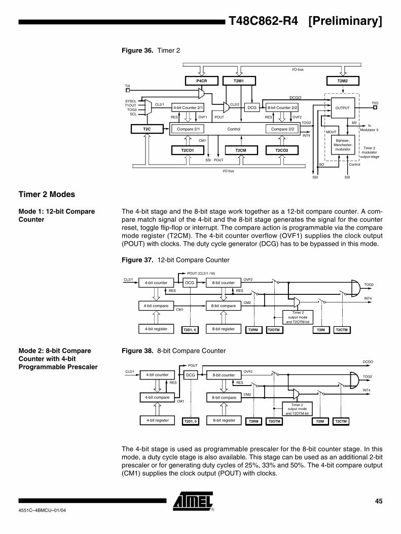
45
T48C862-R4 [Preliminary]
4551C–4BMCU–01/04
Figure 36. Timer 2
Timer 2 Modes
Mode 1: 12-bit Compare Counter
The 4-bit stage and the 8-bit stage work together as a 12-bit compare counter. A com-pare match signal of the 4-bit and the 8-bit stage generates the signal for the counterreset, toggle flip-flop or interrupt. The compare action is programmable via the comparemode register (T2CM). The 4-bit counter overflow (OVF1) supplies the clock output(POUT) with clocks. The duty cycle generator (DCG) has to be bypassed in this mode.
Figure 37. 12-bit Compare Counter
Mode 2: 8-bit Compare Counter with 4-bit Programmable Prescaler
Figure 38. 8-bit Compare Counter
The 4-bit stage is used as programmable prescaler for the 8-bit counter stage. In thismode, a duty cycle stage is also available. This stage can be used as an additional 2-bitprescaler or for generating duty cycles of 25%, 33% and 50%. The 4-bit compare output(CM1) supplies the clock output (POUT) with clocks.
4-bit Counter 2/1
RES OVF1
Compare 2/1
T2CO1
CM1
POUT
SSI POUT
CL2/2DCG
T2M1P4CR
8-bit Counter 2/2
RES OVF2
Compare 2/2
T2CO2T2CM
Control
TOG2
INT4
Biphase-,Manchester-modulator
OUTPUT
MOUT
M2to
Modulator 3
T2O
Timer 2modulator
output-stage
T2M2
SO Control
SSI SSI
I/O-bus
T2C
CL2/1
T2I
SYSCLT1OUT
TOG3SCL
I/O-bus
DCGO
4-bit counter
4-bit compare
RES
4-bit register
CM1
POUT (CL2/1 /16)
8-bit counter
8-bit compare
8-bit register
OVF2
CM2
RES
T2RM T2OTM
Timer 2output mode
and T2OTM-bit
T2IM T2CTM
TOG2
INT4
CL2/1DCG
T2D1, 0
4-bit counter
4-bit compare
RES
4-bit register
CM1
POUT
8-bit counter
8-bit compare
8-bit register
OVF2
CM2
RES
T2RM T2OTM
Timer 2output mode
and T2OTM-bit
T2IM T2CTM
TOG2
INT4
CL2/1DCG
T2D1, 0
DCGO
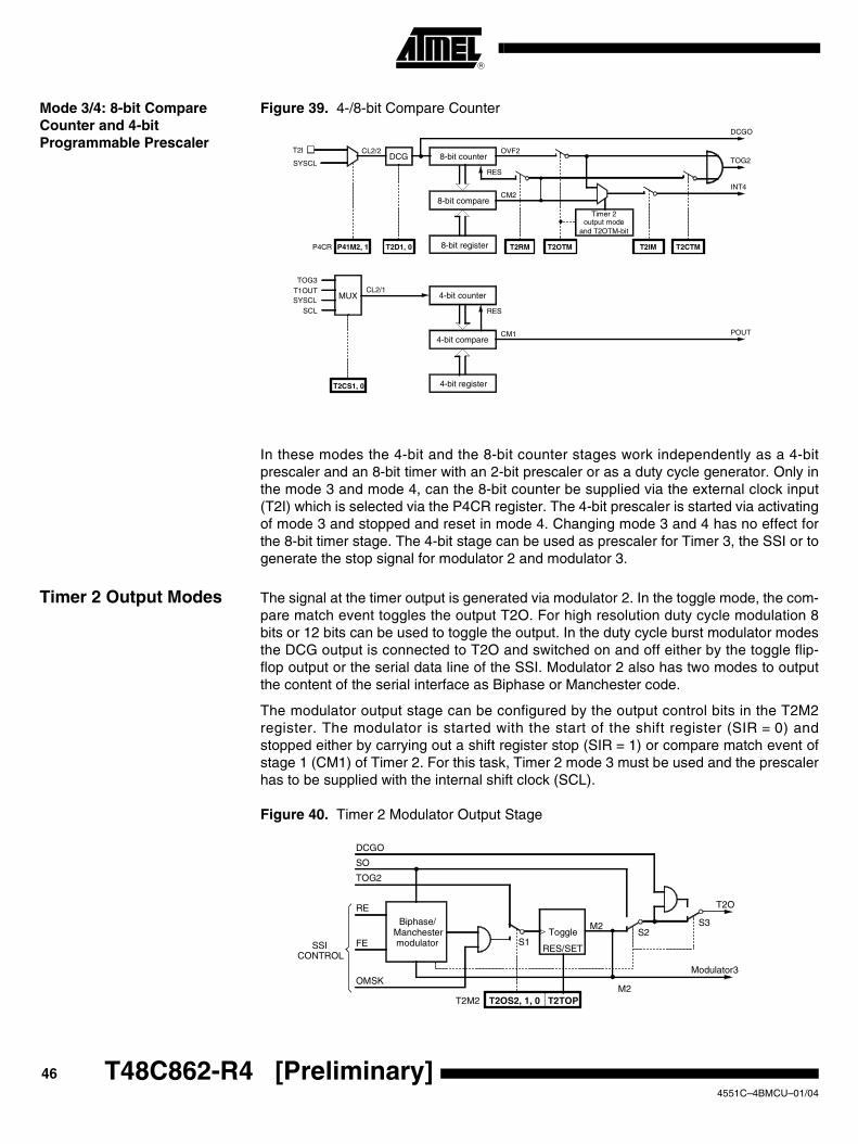
46 T48C862-R4 [Preliminary] 4551C–4BMCU–01/04
Mode 3/4: 8-bit Compare Counter and 4-bit Programmable Prescaler
Figure 39. 4-/8-bit Compare Counter
In these modes the 4-bit and the 8-bit counter stages work independently as a 4-bitprescaler and an 8-bit timer with an 2-bit prescaler or as a duty cycle generator. Only inthe mode 3 and mode 4, can the 8-bit counter be supplied via the external clock input(T2I) which is selected via the P4CR register. The 4-bit prescaler is started via activatingof mode 3 and stopped and reset in mode 4. Changing mode 3 and 4 has no effect forthe 8-bit timer stage. The 4-bit stage can be used as prescaler for Timer 3, the SSI or togenerate the stop signal for modulator 2 and modulator 3.
Timer 2 Output Modes The signal at the timer output is generated via modulator 2. In the toggle mode, the com-pare match event toggles the output T2O. For high resolution duty cycle modulation 8bits or 12 bits can be used to toggle the output. In the duty cycle burst modulator modesthe DCG output is connected to T2O and switched on and off either by the toggle flip-flop output or the serial data line of the SSI. Modulator 2 also has two modes to outputthe content of the serial interface as Biphase or Manchester code.
The modulator output stage can be configured by the output control bits in the T2M2register. The modulator is started with the start of the shift register (SIR = 0) andstopped either by carrying out a shift register stop (SIR = 1) or compare match event ofstage 1 (CM1) of Timer 2. For this task, Timer 2 mode 3 must be used and the prescalerhas to be supplied with the internal shift clock (SCL).
Figure 40. Timer 2 Modulator Output Stage
4-bit counter
4-bit compare
RES
4-bit register
8-bit counter
8-bit compare
8-bit register
OVF2
CM2
RES
T2RM T2OTM
Timer 2output mode
and T2OTM-bit
T2IM T2CTM
TOG2
INT4
CL2/2DCG
T2D1, 0
DCGO
P41M2, 1P4CR
CM1 POUT
CL2/1MUX
TOG3T1OUTSYSCL
SCL
T2CS1, 0
SYSCL
T2I
Toggle
RES/SET
Biphase/Manchestermodulator
T2TOPT2OS2, 1, 0T2M2
T2O
M2
M2
S1S2
S3
Modulator3
RE
FE
OMSK
SSICONTROL
TOG2
SO
DCGO

47
T48C862-R4 [Preliminary]
4551C–4BMCU–01/04
Timer 2 Output Signals
Timer 2 Output Mode 1 Toggle Mode A: A Timer 2 compare match toggles the output flip-flop (M2) -> T2O
Figure 41. Interrupt Timer/Square Wave Generator – the Output Toggles with EachEdge Compare Match Event
Toggle Mode B: A Timer 2 compare match toggles the output flip-flop (M2) -> T2O
Figure 42. Pulse Generator – the Timer Output Toggles with the Timer Start if theT2TS bit Is Set
40 0 0 1 2 3 40 1 2 3 40 1 2 3 0 1
InputCounter 2
T2R
Counter 2
CMx
INT4
T2O
40 0 0 1 2 3 5 6 7 40 1 2 3 5 6
InputCounter 2
T2R
Counter 2
CMx
INT4
T2OToggleby start
T2O
4095/255
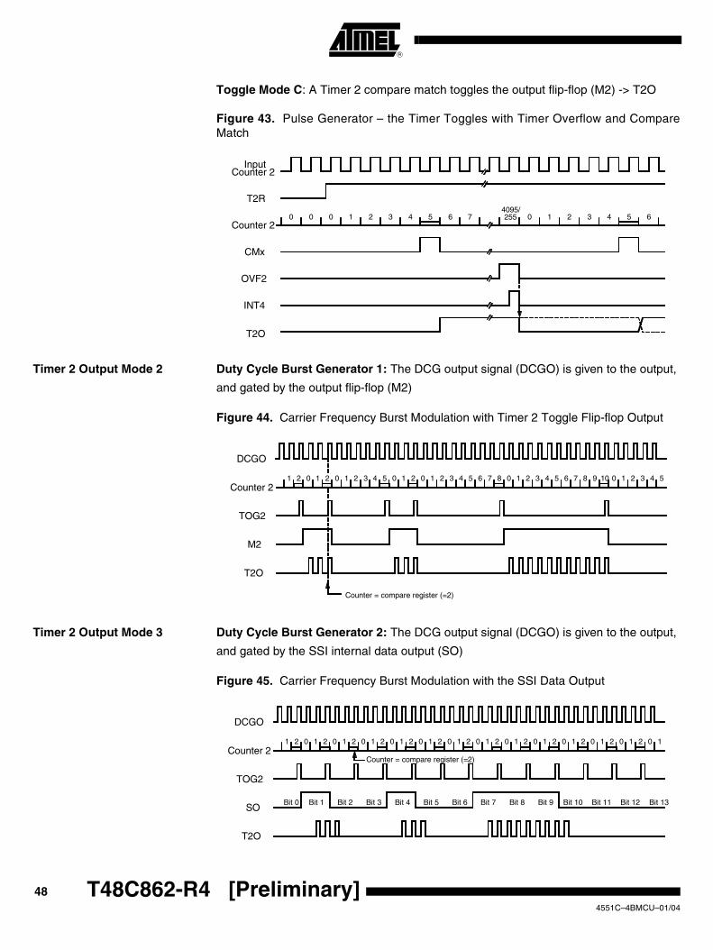
48 T48C862-R4 [Preliminary] 4551C–4BMCU–01/04
Toggle Mode C: A Timer 2 compare match toggles the output flip-flop (M2) -> T2O
Figure 43. Pulse Generator – the Timer Toggles with Timer Overflow and CompareMatch
Timer 2 Output Mode 2 Duty Cycle Burst Generator 1: The DCG output signal (DCGO) is given to the output,
and gated by the output flip-flop (M2)
Figure 44. Carrier Frequency Burst Modulation with Timer 2 Toggle Flip-flop Output
Timer 2 Output Mode 3 Duty Cycle Burst Generator 2: The DCG output signal (DCGO) is given to the output,
and gated by the SSI internal data output (SO)
Figure 45. Carrier Frequency Burst Modulation with the SSI Data Output
40 0 0 1 2 3 5 6 7 40 1 2 3 5 6
InputCounter 2
T2R
Counter 2
CMx
OVF2
INT4
T2O
4095/255
1 2 0 1 2 0 1 2 3 4 5 0 1 2 0 1 2 3 4 5 6 7 8 0 1 2 3 4 5 6 7 8 9 10 0 1 2 3 4 5
DCGO
Counter 2
TOG2
M2
T2O
Counter = compare register (=2)
1 2 0 1 2 0 1 2 0 1 2 0 1 2 0 1 2 0 1 2 0 1 2 0 1 2 0 1 2 0 1 2 0 1 2 0 1 2 0 1
DCGO
Counter 2
TOG2
SO
T2O
Counter = compare register (=2)
Bit 0 Bit 1 Bit 2 Bit 3 Bit 4 Bit 5 Bit 6 Bit 7 Bit 8 Bit 9 Bit 10 Bit 11 Bit 12 Bit 13
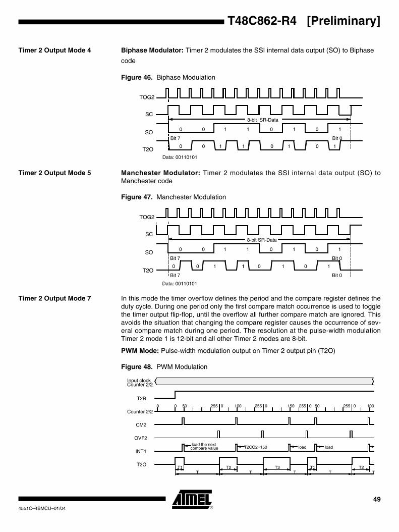
49
T48C862-R4 [Preliminary]
4551C–4BMCU–01/04
Timer 2 Output Mode 4 Biphase Modulator: Timer 2 modulates the SSI internal data output (SO) to Biphase
code
Figure 46. Biphase Modulation
Timer 2 Output Mode 5 Manchester Modulator: Timer 2 modulates the SSI internal data output (SO) toManchester code
Figure 47. Manchester Modulation
Timer 2 Output Mode 7 In this mode the timer overflow defines the period and the compare register defines theduty cycle. During one period only the first compare match occurrence is used to togglethe timer output flip-flop, until the overflow all further compare match are ignored. Thisavoids the situation that changing the compare register causes the occurrence of sev-eral compare match during one period. The resolution at the pulse-width modulationTimer 2 mode 1 is 12-bit and all other Timer 2 modes are 8-bit.
PWM Mode: Pulse-width modulation output on Timer 2 output pin (T2O)
Figure 48. PWM Modulation
TOG2
SC
SO
T2O0 0 00
0 0 1 1 0 1 0 1
1 1 1 1
8-bit SR-Data
Bit 7 Bit 0
Data: 00110101
TOG2
SC
SO
T2O0 00
0 0 1 1 0 1 0 1
1 1 1 1
8-bit SR-Data
Bit 7 Bit 0
0
Bit 7 Bit 0
Data: 00110101
0 0 50 255 1000 255 0 150 255 0 50 255 0 100
T2R
Input clockCounter 2/2
Counter 2/2
OVF2
CM2
INT4
T2O
load the nextcompare value T2CO2=150 load load
T1 T2 T3 T1 T2T T T T T
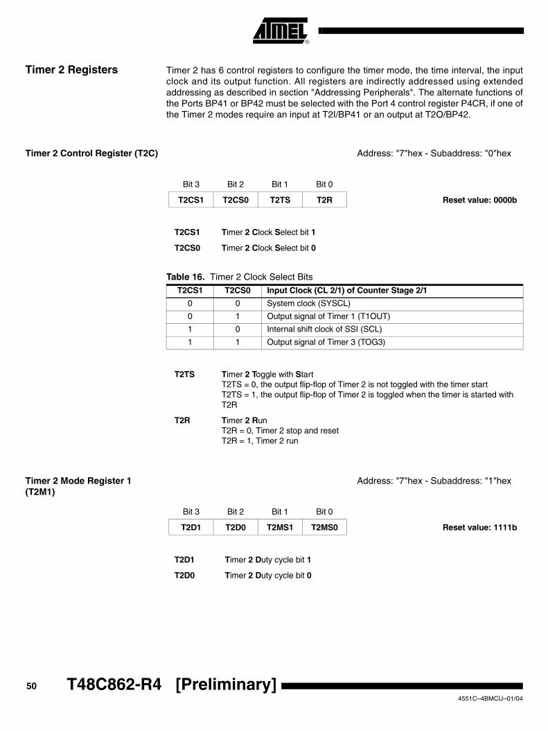
50 T48C862-R4 [Preliminary] 4551C–4BMCU–01/04
Timer 2 Registers Timer 2 has 6 control registers to configure the timer mode, the time interval, the inputclock and its output function. All registers are indirectly addressed using extendedaddressing as described in section "Addressing Peripherals". The alternate functions ofthe Ports BP41 or BP42 must be selected with the Port 4 control register P4CR, if one ofthe Timer 2 modes require an input at T2I/BP41 or an output at T2O/BP42.
Timer 2 Control Register (T2C) Address: "7"hex - Subaddress: "0"hex
Table 16. Timer 2 Clock Select Bits
Timer 2 Mode Register 1 (T2M1)
Address: "7"hex - Subaddress: "1"hex
Bit 3 Bit 2 Bit 1 Bit 0
T2CS1 T2CS0 T2TS T2R Reset value: 0000b
T2CS1 Timer 2 Clock Select bit 1
T2CS0 Timer 2 Clock Select bit 0
T2CS1 T2CS0 Input Clock (CL 2/1) of Counter Stage 2/1
0 0 System clock (SYSCL)
0 1 Output signal of Timer 1 (T1OUT)
1 0 Internal shift clock of SSI (SCL)
1 1 Output signal of Timer 3 (TOG3)
T2TS Timer 2 Toggle with StartT2TS = 0, the output flip-flop of Timer 2 is not toggled with the timer startT2TS = 1, the output flip-flop of Timer 2 is toggled when the timer is started with T2R
T2R Timer 2 RunT2R = 0, Timer 2 stop and resetT2R = 1, Timer 2 run
Bit 3 Bit 2 Bit 1 Bit 0
T2D1 T2D0 T2MS1 T2MS0 Reset value: 1111b
T2D1 Timer 2 Duty cycle bit 1
T2D0 Timer 2 Duty cycle bit 0
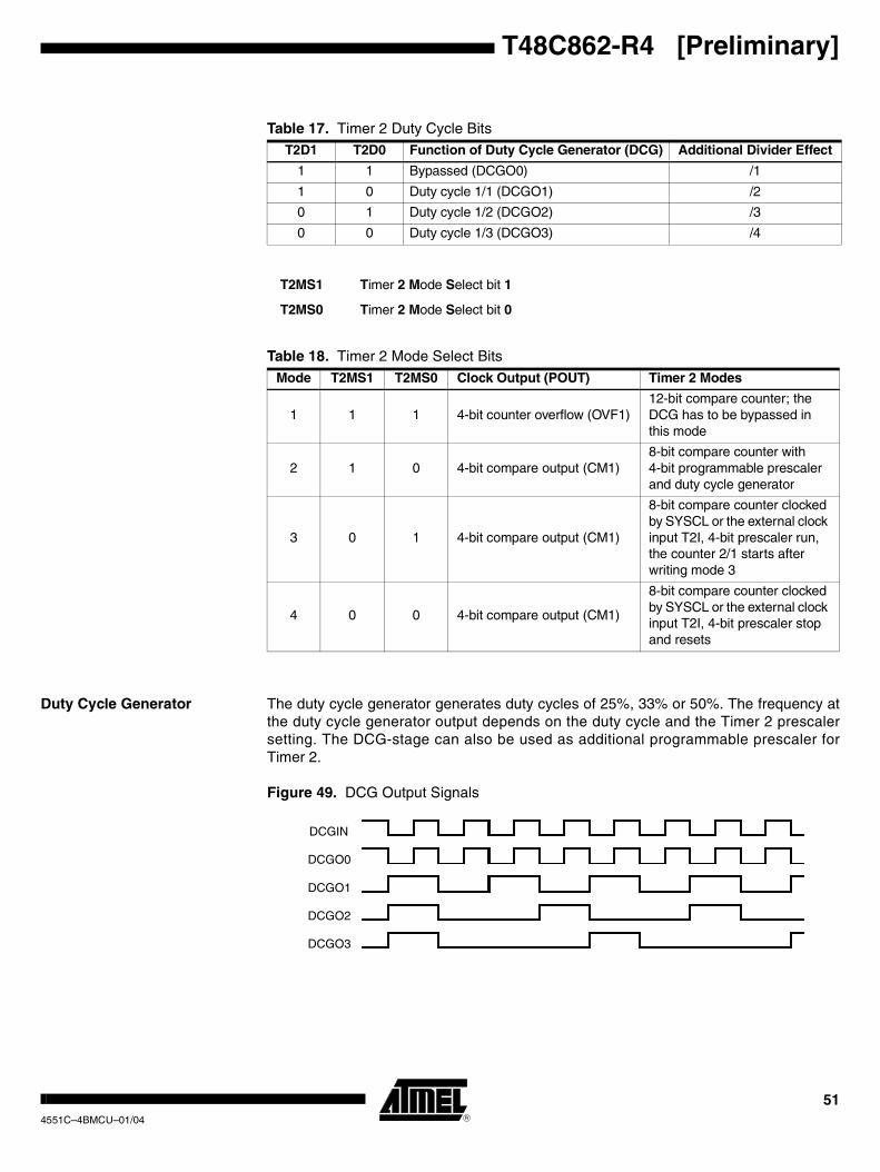
51
T48C862-R4 [Preliminary]
4551C–4BMCU–01/04
Table 17. Timer 2 Duty Cycle Bits
Table 18. Timer 2 Mode Select Bits
Duty Cycle Generator The duty cycle generator generates duty cycles of 25%, 33% or 50%. The frequency atthe duty cycle generator output depends on the duty cycle and the Timer 2 prescalersetting. The DCG-stage can also be used as additional programmable prescaler forTimer 2.
Figure 49. DCG Output Signals
T2D1 T2D0 Function of Duty Cycle Generator (DCG) Additional Divider Effect
1 1 Bypassed (DCGO0) /1
1 0 Duty cycle 1/1 (DCGO1) /2
0 1 Duty cycle 1/2 (DCGO2) /3
0 0 Duty cycle 1/3 (DCGO3) /4
T2MS1 Timer 2 Mode Select bit 1
T2MS0 Timer 2 Mode Select bit 0
Mode T2MS1 T2MS0 Clock Output (POUT) Timer 2 Modes
1 1 1 4-bit counter overflow (OVF1)12-bit compare counter; the DCG has to be bypassed in this mode
2 1 0 4-bit compare output (CM1)8-bit compare counter with 4-bit programmable prescaler and duty cycle generator
3 0 1 4-bit compare output (CM1)
8-bit compare counter clocked by SYSCL or the external clock input T2I, 4-bit prescaler run, the counter 2/1 starts after writing mode 3
4 0 0 4-bit compare output (CM1)
8-bit compare counter clocked by SYSCL or the external clock input T2I, 4-bit prescaler stop and resets
DCGIN
DCGO0
DCGO1
DCGO2
DCGO3
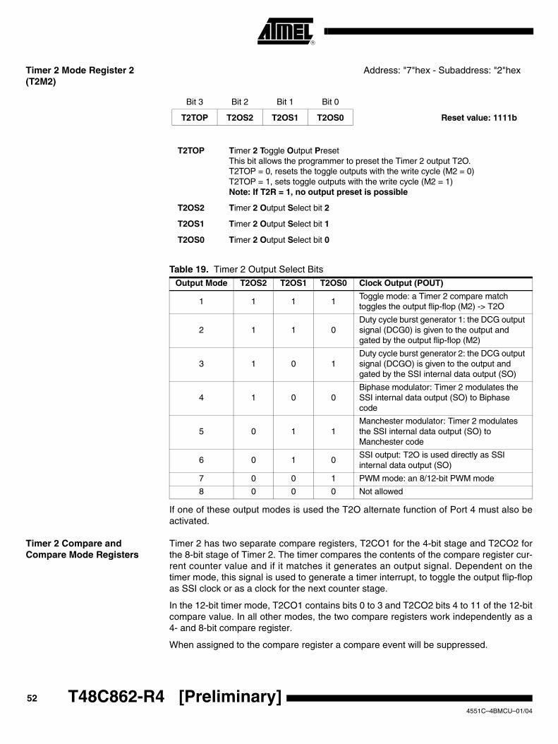
52 T48C862-R4 [Preliminary] 4551C–4BMCU–01/04
Timer 2 Mode Register 2 (T2M2)
Address: "7"hex - Subaddress: "2"hex
Table 19. Timer 2 Output Select Bits
If one of these output modes is used the T2O alternate function of Port 4 must also beactivated.
Timer 2 Compare and Compare Mode Registers
Timer 2 has two separate compare registers, T2CO1 for the 4-bit stage and T2CO2 forthe 8-bit stage of Timer 2. The timer compares the contents of the compare register cur-rent counter value and if it matches it generates an output signal. Dependent on thetimer mode, this signal is used to generate a timer interrupt, to toggle the output flip-flopas SSI clock or as a clock for the next counter stage.
In the 12-bit timer mode, T2CO1 contains bits 0 to 3 and T2CO2 bits 4 to 11 of the 12-bitcompare value. In all other modes, the two compare registers work independently as a4- and 8-bit compare register.
When assigned to the compare register a compare event will be suppressed.
Bit 3 Bit 2 Bit 1 Bit 0
T2TOP T2OS2 T2OS1 T2OS0 Reset value: 1111b
T2TOP Timer 2 Toggle Output PresetThis bit allows the programmer to preset the Timer 2 output T2O.T2TOP = 0, resets the toggle outputs with the write cycle (M2 = 0)T2TOP = 1, sets toggle outputs with the write cycle (M2 = 1)Note: If T2R = 1, no output preset is possible
T2OS2 Timer 2 Output Select bit 2
T2OS1 Timer 2 Output Select bit 1
T2OS0 Timer 2 Output Select bit 0
Output Mode T2OS2 T2OS1 T2OS0 Clock Output (POUT)
1 1 1 1Toggle mode: a Timer 2 compare match toggles the output flip-flop (M2) -> T2O
2 1 1 0Duty cycle burst generator 1: the DCG output signal (DCG0) is given to the output and gated by the output flip-flop (M2)
3 1 0 1Duty cycle burst generator 2: the DCG output signal (DCGO) is given to the output and gated by the SSI internal data output (SO)
4 1 0 0Biphase modulator: Timer 2 modulates the SSI internal data output (SO) to Biphase code
5 0 1 1Manchester modulator: Timer 2 modulates the SSI internal data output (SO) to Manchester code
6 0 1 0SSI output: T2O is used directly as SSI internal data output (SO)
7 0 0 1 PWM mode: an 8/12-bit PWM mode
8 0 0 0 Not allowed
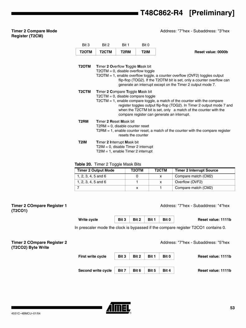
53
T48C862-R4 [Preliminary]
4551C–4BMCU–01/04
Timer 2 Compare Mode Register (T2CM)
Address: "7"hex - Subaddress: "3"hex
Table 20. Timer 2 Toggle Mask Bits
Timer 2 COmpare Register 1 (T2CO1)
Address: "7"hex - Subaddress: "4"hex
In prescaler mode the clock is bypassed if the compare register T2CO1 contains 0.
Timer 2 COmpare Register 2 (T2CO2) Byte Write
Address: "7"hex - Subaddress: "5"hex
Bit 3 Bit 2 Bit 1 Bit 0
T2OTM T2CTM T2RM T2IM Reset value: 0000b
T2OTM Timer 2 Overflow Toggle Mask bitT2OTM = 0, disable overflow toggleT2OTM = 1, enable overflow toggle, a counter overflow (OVF2) toggles output
flip-flop (TOG2). If the T2OTM bit is set, only a counter overflow cangenerate an interrupt except on the Timer 2 output mode 7.
T2CTM Timer 2 Compare Toggle Mask bitT2CTM = 0, disable compare toggleT2CTM = 1, enable compare toggle, a match of the counter with the compare
register toggles output flip-flop (TOG2). In Timer 2 output mode 7 andwhen the T2CTM bit is set, only a match of the counter with thecompare register can generate an interrupt.
T2RM Timer 2 Reset Mask bitT2RM = 0, disable counter resetT2RM = 1, enable counter reset, a match of the counter with the compare register
resets the counter
T2IM Timer 2 Interrupt Mask bitT2IM = 0, disable Timer 2 interruptT2IM = 1, enable Timer 2 interrupt
Timer 2 Output Mode T2OTM T2CTM Timer 2 Interrupt Source
1, 2, 3, 4, 5 and 6 0 x Compare match (CM2)
1, 2, 3, 4, 5 and 6 1 x Overflow (OVF2)
7 x 1 Compare match (CM2)
Write cycle Bit 3 Bit 2 Bit 1 Bit 0 Reset value: 1111b
First write cycle Bit 3 Bit 2 Bit 1 Bit 0 Reset value: 1111b
Second write cycle Bit 7 Bit 6 Bit 5 Bit 4 Reset value: 1111b
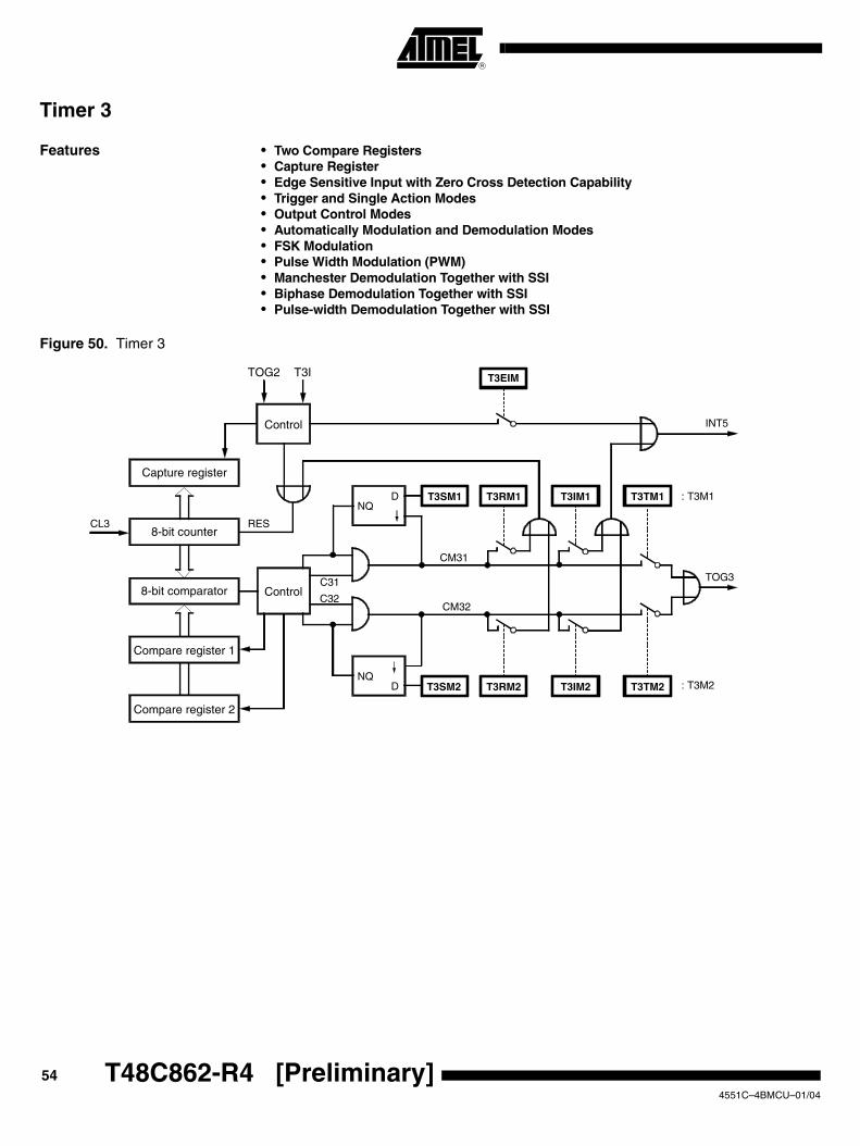
54 T48C862-R4 [Preliminary] 4551C–4BMCU–01/04
Timer 3
Features • Two Compare Registers• Capture Register• Edge Sensitive Input with Zero Cross Detection Capability• Trigger and Single Action Modes• Output Control Modes• Automatically Modulation and Demodulation Modes• FSK Modulation• Pulse Width Modulation (PWM)• Manchester Demodulation Together with SSI• Biphase Demodulation Together with SSI• Pulse-width Demodulation Together with SSI
Figure 50. Timer 3
8-bit comparator
Compare register 1
RES
Capture register
8-bit counter
Compare register 2
ControlC31
C32
Control
T3SM1NQ
D T3RM1 T3IM1 T3TM1
TOG2 T3I
T3TM2T3IM2T3RM2T3SM2NQ
D
CL3
T3EIM
TOG3
INT5
CM31
CM32
: T3M1
: T3M2

55
T48C862-R4 [Preliminary]
4551C–4BMCU–01/04
Timer 3 consists of an 8-bit up-counter with two compare registers and one capture reg-ister. The timer can be used as event counter, timer and signal generator. Its output canbe programmed as modulator and demodulator for the serial interface. The two com-pare registers enable various modes of signal generation, modulation anddemodulation. The counter can be driven by internal and external clock sources. Forexternal clock sources, it has a programmable edge-sensitive input which can be usedas counter input, capture signal input or trigger input. This timer input is synchronizedwith SYSCL. Therefore, in the power-down mode SLEEP (CPU core -> sleep and OSC-Stop -> yes), this timer input is stopped too. The counter is readable via its capture reg-ister while it is running. In capture mode, the counter value can be captured by aprogrammable capture event from the Timer 3 input or Timer 2 output.
A special feature of this timer is the trigger- and single-action mode. In trigger mode, thecounter starts counting triggered by the external signal at its input. In single-actionmode, the counter counts only one time up to the programmed compare match event.These modes are very useful for modulation, demodulation, signal generation, signalmeasurement and phase controlling. For phase controlling, the timer input is protectedagainst negative voltages and has zero-cross detection capability.
Timer 3 has a modulator output stage and input functions for demodulation. As modula-tor it works together with Timer 2 or the serial interface. When the shift register is usedfor modulation the data shifted out of the register is encoded bitwise. In all demodulationmodes, the decoded data bits are shifted automatically into the shift register.
Timer/Counter Modes Timer 3 has 6 timer modes and 6 modulator/demodulator modes. The mode is set viathe Timer 3 Mode Register T3M.
In all these modes, the compare register and the compare-mode register belonging to itdefine the counter value for a compare match and the action of a compare match. Amatch of the current counter value with the content of one compare register triggers acounter reset, a Timer 3 interrupt or the toggling of the output flip-flop. The comparemode registers T3M1 and T3M2 contain the mask bits for enabling or disabling theseactions.
The counter can also be enabled to execute single actions with one or both compareregisters. If this mode is set the corresponding compare match event is generated onlyonce after the counter start.
Most of the timer modes use their compare registers alternately. After the start has beenactivated, the first comparison is carried out via the compare register 1, the second iscarried out via the compare register 2, the third is carried out again via the compare reg-ister 1 and so on. This makes it easy to generate signals with constant periods andvariable duty cycle or to generate signals with variable pulse and space widths.
If single-action mode is set for one compare register, the comparison is always carriedout after the first cycle via the other compare register.
The counter can be started and stopped via the control register T3C. This register alsocontrols the initial level of the output before start. T3C contains the interrupt mask for aT3I input interrupt.
Via the Timer 3 clock-select register, the internal or external clock source can beselected. This register selects also the active edge of the external input. An edge at theexternal input T3I can generate also an interrupt if the T3EIM bit is set and the Timer 3 isstopped (T3R = 0) in the T3C register.

56 T48C862-R4 [Preliminary] 4551C–4BMCU–01/04
Figure 51. Counter 3 Stage
The status of the timer as well as the occurrence of a compare match or an edge detectof the input signal is indicated by the status register T2ST. This allows identification ofthe interrupt source because all these events share only one timer interrupt.
Timer 3 compares data values.
The Timer 3 has two 8-bit compare registers (T3CO1, T3CO2). The compare data valuecan be ‘m’ for each of the Timer 3 compare registers.
The compare data value for the compare registers is: m = x +1 0 ≤ x ≤ 255
Timer 3 – Mode 1: Timer/Counter
The selected clock from an internal or external source increments the 8-bit counter. Inthis mode, the timer can be used as event counter for external clocks at T3I or as timerfor generating interrupts and pulses at T3O. The counter value can be read by the soft-ware via the capture register.
8-bit comparator
Compare register 1
RES
Capture register
8-bit counter
Compare register 2
ControlC31
C32
Control
T3SM1NQ
D T3RM1 T3IM1 T3TM1
TOG2 T3I
T3TM2T3IM2T3RM2T3SM2NQ
D
CL3
T3EIM
TOG3
INT5
CM31
CM32
: T3M1
: T3M2

57
T48C862-R4 [Preliminary]
4551C–4BMCU–01/04
Figure 52. Counter Reset with Each Compare Match
Figure 53. Counter Reset with Compare Register 2 and Toggle with Start
Figure 54. Single Action of Compare Register 1
Timer 3 – Mode 2: Timer/Counter, External Trigger Restart and External Capture (with T3I Input)
The counter is driven by an internal clock source. After starting with T3R, the first edgefrom the external input T3I starts the counter. The following edges at T3I load the cur-rent counter value into the capture register, reset the counter and restart it. The edgecan be selected by the programmable edge decoder of the timer input stage. If single-action mode is activated for one or both compare registers the trigger signal restarts thesingle action.
00 0 0 1 2 3 51 2 3 4 00 1 2 3 1 2
T3R
Counter 3
CM31
INT5
T3O
3
CM32
40 0 0 1 2 3 5 6 7 40 1 2 3 5 6
T3R
Counter 3
CM31
INT5
T3O
Toggleby start
T3O
8 9
CL3
CM32
0 0 1 2 3 4 5 6 7 8 9 10 0 1 2Counter 3
CM31
CM32
T3O
0 1 2 0 1 2 0 1 2 0 1 2 0 1 2 0 1 2 0 1 2 0 1 2 0 1
Toggle by start
T3R

58 T48C862-R4 [Preliminary] 4551C–4BMCU–01/04
Figure 55. Externally Triggered Counter Reset and Start Combined with Single-actionMode
Timer 3 – Mode 3: Timer/Counter, Internal Trigger Restart and Internal Capture (with TOG2)
The counter is driven by an internal or external (T3I) clock source. The output toggle sig-nal of Timer 2 resets the counter. The counter value before the reset is saved in thecapture register. If single-action mode is activated for one or both compare registers, thetrigger signal restarts the single actions. This mode can be used for frequency measure-ments or as event counter with time gate (see “Combination Mode 10: FrequencyMeasurement or Event Counter with Time Gate” on page 85).
Figure 56. Event Counter with Time Gate
Timer 3 – Mode 4: Timer/Counter
The timer runs as timer/counter in mode 1, but its output T3O is used as output for theTimer 2 output signal.
Timer 3 – Mode 5: Timer/Counter, External Trigger Restart and External Capture (with T3I Input)
The Timer 3 runs as timer/counter in mode 2, but its output T3O is used as output for theTimer 2 output signal.
Timer 3 Modulator/Demodulator Modes
Timer 3 – Mode 6: Carrier Frequency Burst Modulation Controlled by Timer 2 Output Toggle Flip-Flop (M2)
The Timer 3 counter is driven by an internal or external clock source. Its compare- andcompare mode registers must be programmed to generate the carrier frequency via theoutput toggle flip-flop. The output toggle flip-flop of Timer 2 is used to enable or disablethe Timer 3 output. Timer 2 can be driven by the toggle output signal of Timer 3 or anyother clock source (see “Combination Mode 11: Burst Modulation 1” on page 86).
0 0 0 0 0 0 0 0 1 2 3 4 5 6Counter 3
T3EX
CM31
CM32
7 8 9 10 0 1 2 X X X 0 1 2 3 4 5 6 7 8 9 10 0 1 2 X X
T3R
X X
T3O
0 0 1 2 3 4 5 6 7 8 9 10Counter 3
TOG2
T3CP-Register
11 0 1 2 4 0 1
T3I
23
T3R
Capture value = 0 Capture value = 11 Capturevalue = 4
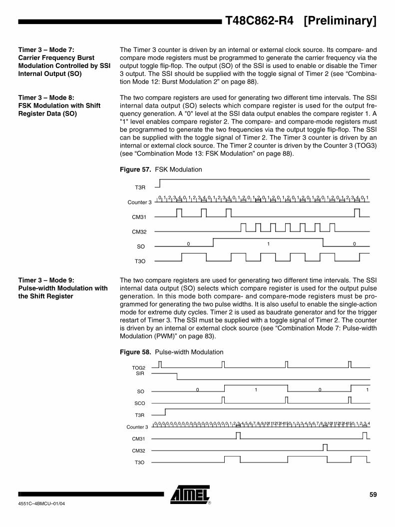
59
T48C862-R4 [Preliminary]
4551C–4BMCU–01/04
Timer 3 – Mode 7: Carrier Frequency Burst Modulation Controlled by SSI Internal Output (SO)
The Timer 3 counter is driven by an internal or external clock source. Its compare- andcompare mode registers must be programmed to generate the carrier frequency via theoutput toggle flip-flop. The output (SO) of the SSI is used to enable or disable the Timer3 output. The SSI should be supplied with the toggle signal of Timer 2 (see “Combina-tion Mode 12: Burst Modulation 2” on page 88).
Timer 3 – Mode 8: FSK Modulation with Shift Register Data (SO)
The two compare registers are used for generating two different time intervals. The SSIinternal data output (SO) selects which compare register is used for the output fre-quency generation. A "0" level at the SSI data output enables the compare register 1. A"1" level enables compare register 2. The compare- and compare-mode registers mustbe programmed to generate the two frequencies via the output toggle flip-flop. The SSIcan be supplied with the toggle signal of Timer 2. The Timer 3 counter is driven by aninternal or external clock source. The Timer 2 counter is driven by the Counter 3 (TOG3)(see “Combination Mode 13: FSK Modulation” on page 88).
Figure 57. FSK Modulation
Timer 3 – Mode 9: Pulse-width Modulation with the Shift Register
The two compare registers are used for generating two different time intervals. The SSIinternal data output (SO) selects which compare register is used for the output pulsegeneration. In this mode both compare- and compare-mode registers must be pro-grammed for generating the two pulse widths. It is also useful to enable the single-actionmode for extreme duty cycles. Timer 2 is used as baudrate generator and for the triggerrestart of Timer 3. The SSI must be supplied with a toggle signal of Timer 2. The counteris driven by an internal or external clock source (see “Combination Mode 7: Pulse-widthModulation (PWM)” on page 83).
Figure 58. Pulse-width Modulation
0 1 2 3 4 0 1 2 3 4 0 1 2 3Counter 3
CM31
CM32
SO
4 0 1 2 0 1 2 0 1 2 0 1 2 0 1 2 0 1 2 0 1 2 0 1 2 3
T3R
4 0
T3O
1
0 1 0
0 0 0 0 0 0 0 0 0 0 0 0 0Counter 3
CM31
CM32
T3O
0 0 0 0 0 1 2 3 4 5 6 7 8 9 1011121314150 1 2 3 4 5
TOG2
6 7 8
1
9 111210 1413 0 2 31 4150
00 1
SIR
SO
SCO
T3R
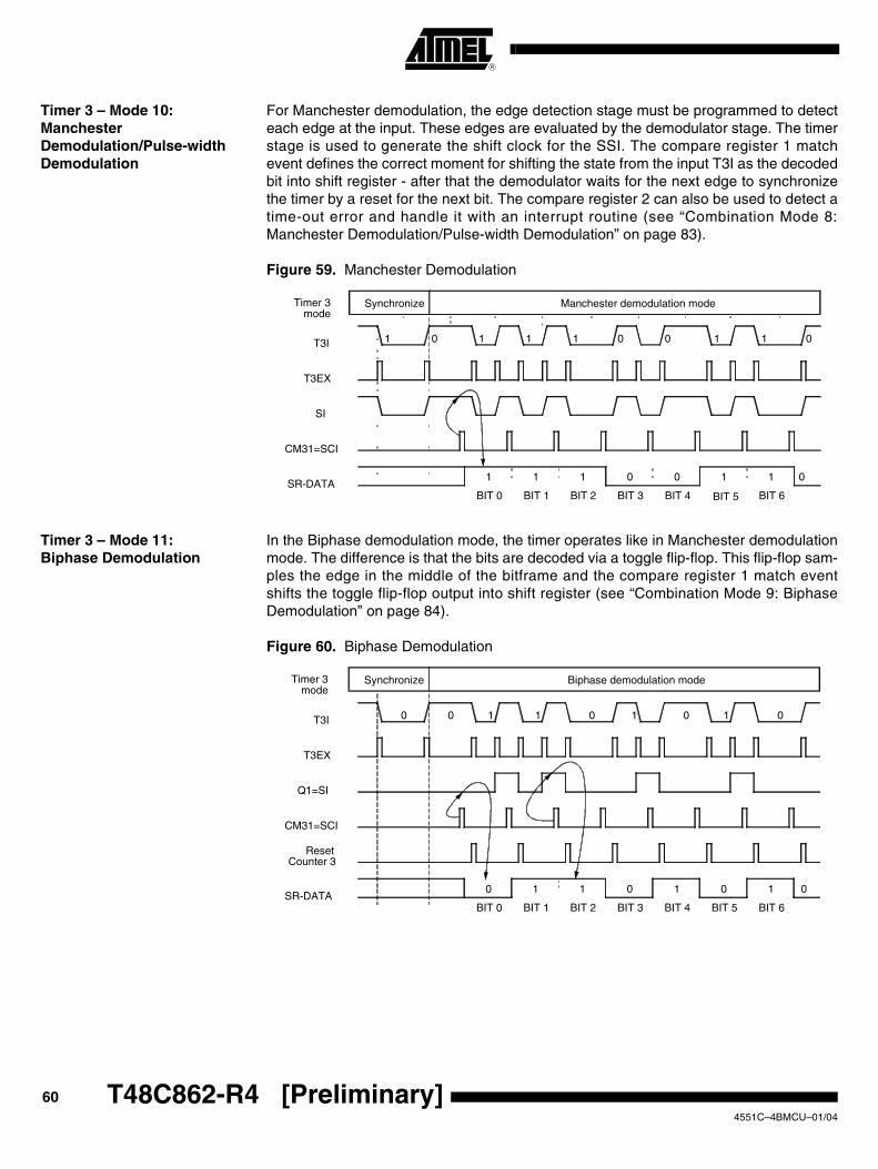
60 T48C862-R4 [Preliminary] 4551C–4BMCU–01/04
Timer 3 – Mode 10: Manchester Demodulation/Pulse-width Demodulation
For Manchester demodulation, the edge detection stage must be programmed to detecteach edge at the input. These edges are evaluated by the demodulator stage. The timerstage is used to generate the shift clock for the SSI. The compare register 1 matchevent defines the correct moment for shifting the state from the input T3I as the decodedbit into shift register - after that the demodulator waits for the next edge to synchronizethe timer by a reset for the next bit. The compare register 2 can also be used to detect atime-out error and handle it with an interrupt routine (see “Combination Mode 8:Manchester Demodulation/Pulse-width Demodulation” on page 83).
Figure 59. Manchester Demodulation
Timer 3 – Mode 11: Biphase Demodulation
In the Biphase demodulation mode, the timer operates like in Manchester demodulationmode. The difference is that the bits are decoded via a toggle flip-flop. This flip-flop sam-ples the edge in the middle of the bitframe and the compare register 1 match eventshifts the toggle flip-flop output into shift register (see “Combination Mode 9: BiphaseDemodulation” on page 84).
Figure 60. Biphase Demodulation
1 0 1 1 1 0 0 1 1 0
1 1
BIT 0 BIT 1 BIT 2 BIT 3 BIT 4 BIT 5 BIT 6
Synchronize Manchester demodulation modeTimer 3mode
T3EX
SI
SR-DATA
T3I
CM31=SCI
1 0 0 1 1 0
0 1 1 1 1
0 1
BIT 0 BIT 1 BIT 2 BIT 3 BIT 4 BIT 5 BIT 6
Synchronize Biphase demodulation modeTimer 3mode
T3EX
Q1=SI
CM31=SCI
SR-DATA
0 0 0 0T3I
ResetCounter 3
1 0 1 0 1 0
61
T48C862-R4 [Preliminary]
4551C–4BMCU–01/04
Timer 3 – Mode 12: Timer/Counter with External Capture Mode (T3I)
The counter is driven by an internal clock source and an edge at the external input T3Iloads the counter value into the capture register. The edge can be selected with the pro-grammable edge detector of the timer input stage. This mode can be used for signal andpulse measurements.
Figure 61. External Capture Mode
Timer 3 Modulator for Carrier Frequency Burst Modulation
If the output stage operates as pulse-width modulator for the shift register, the outputcan be stopped with stage 1 of Timer 2. For this task, the timer mode 3 must be usedand the prescaler must be supplied by the internal shift clock of the shift register.
The modulator can be started with the start of the shift register (SIR = 0) and stoppedeither by a shift register stop (SIR = 1) or compare match event of stage 1 of Timer 2.For this task, the Timer 2 must be used in mode 3 and the prescaler stage must be sup-plied by the internal shift clock of the shift register.
Figure 62. Modulator 3
Timer 3 Demodulator for Biphase, Manchester and Pulse-width-modulated Signals
The demodulator stage of Timer 3 can be used to decode Biphase, Manchester andpulse-width-coded signals.
Figure 63. Timer 3 Demodulator 3
0 1 2 3 4 5 6 7 8 9 1011Counter 3
T3CP-Register
15
T3I
T3R
Capture value = X Capture value = 17 Capturevalue = 35
0 121314 16 20171819 2221 23 27242526 2928 30 34313233 3635 37 41383940
T3
Set Res
T3OT3TOP
OMSK
TOG3
SO
SSI/Control
M2
M3
MUX
T3M
0
1
2
3
Timer 3 Mode T3O
6 MUX 17 MUX 29 MUX 3
other MUX 0
Demodulator 3
T3EX Res
CM31 Counter 3Reset
Counter 3Control
SCI
SI
T3I
T3M
62 T48C862-R4 [Preliminary] 4551C–4BMCU–01/04
Timer 3 Registers
Timer 3 Mode Register (T3M) Address: "B"hex - Subaddress: "0"hex
Table 21. Timer 3 Mode Seledt Bits
Note: 1. In this mode, the SSI can be used only as demodulator (8-bit NRZ rising edge). Allother SSI modes are not allowed.
Bit 3 Bit 2 Bit 1 Bit 0
T3M3 T3M2 T3M1 T3M0 Reset value: 1111b
T3M3 Timer 3 Mode select bit 3
T3M2 Timer 3 Mode select bit 2
T3M1 Timer 3 Mode select bit 1
T3M0 Timer 3 Mode select bit 0
Mode T3M3 T3M2 T3M1 T3M0 Timer 3 Modes
1 1 1 1 1 Timer/counter with a read access
2 1 1 1 0Timer/counter, external capture and external trigger restart mode (T3I)
3 1 1 0 1Timer/counter, internal capture and internal trigger restart mode (TOG2)
4 1 1 0 0Timer/counter mode 1 without output (T2O -> T3O)
5 1 0 1 1Timer/counter mode 2 without output (T2O -> T3O)
6 1 0 1 0 Burst modulation with Timer 2 (M2)
7 1 0 0 1 Burst modulation with shift register (SO)
8 1 0 0 0 FSK modulation with shift register (SO)
9 0 1 1 1Pulse-width modulation with shift register (SO) and Timer 2 (TOG2), internal trigger restart (SCO) -> counter reset
10 0 1 1 0Manchester demodulation/pulse-width demodulation (1) (T2O -> T3O)
11 0 1 0 1 Biphase demodulation (T2O -> T3O)
12 0 1 0 0 Timer/counter with external capture mode (T3I)
13 0 0 1 1 Not allowed
14 0 0 1 0 Not allowed
15 0 0 0 1 Not allowed
16 0 0 0 0 Not allowed
63
T48C862-R4 [Preliminary]
4551C–4BMCU–01/04
Timer 3 Control Register 1 (T3C) Write
Primary register address: "C"hex - Write
Timer 3 Status Register 1 (T3ST) Read
Primary register address: "C"hex - Read
Note: The status bits T3C1, T3C2 and T3ED will be reset after a READ access to T3ST.
Bit 3 Bit 2 Bit 1 Bit 0
Write T3EIM T3TOP T3TS T3R Reset value: 0000b
T3EIM Timer 3 Edge Interrupt MaskT3EIM = 0, disables the interrupt when an edge event for Timer 3 occurs (T3I)T3EIM = 1, enables the interrupt when an edge event for Timer 3 occurs (T3I)
T3TOP Timer 3 Toggle Output Preset T3TOP = 0, sets toggle output (M3) to "0"T3TOP = 1, sets toggle output (M3) to "1"Note: If T3R = 1, no output preset is possible
T3TS Timer 3 Toggle with Start T3TS = 0, Timer 3 output is not toggled during the startT3TS = 1, Timer 3 output is toggled if started with T3R
T3R Timer 3 Run T3R = 0, Timer 3 stop and resetT3R = 1, Timer 3 run
Bit 3 Bit 2 Bit 1 Bit 0
Read – T3ED T3C2 T3C1 Reset value: x000b
T3ED Timer 3 Edge DetectThis bit will be set by the edge-detect logic of Timer 3 input (T3I)
T3C2 Timer 3 Compare 2This bit will be set when a match occurs between Counter 3 and T3CO2
T3C1 Timer 3 Compare 1This bit will be set when a match occurs between Counter 3 and T3CO1
64 T48C862-R4 [Preliminary] 4551C–4BMCU–01/04
Timer 3 Clock Select Register (T3CS)
Address: "B"hex - Subaddress: "1"hex
Table 22. Timer 3 Edge Select Bits
Table 23. Timer 3 Clock Select Bits
Timer 3 Compare- and Compare-mode Register
Timer 3 has two separate compare registers T3CO1 and T3CO2 for the 8-bit stage ofTimer 3. The timer compares the content of the compare register with the currentcounter value. If both match, it generates a signal. This signal can be used for thecounter reset, to generate a timer interrupt, for toggling the output flip-flop, as SSI clockor as clock for the next counter stage. For each compare register, a compare-mode reg-ister exists. These registers contain mask bits to enable or disable the generation of aninterrupt, a counter reset, or an output toggling with the occurrence of a compare matchof the corresponding compare register. The mask bits for activating the single-actionmode can also be located in the compare mode registers. When assigned to the com-pare register a compare event will be suppressed.
Bit 3 Bit 2 Bit 1 Bit 0
T3CS T3E1 T3E0 T3CS1 T3CS0 Reset value: 1111b
T3E1 Timer 3 Edge select bit 1
T3E0 Timer 3 Edge select bit 0
T3E1 T3E0 Timer 3 Input Edge Select (T3I)
1 1 –
1 0 Positive edge at T3I pin
0 1 Negative edge at T3I pin
0 0 Each edge at T3I pin
T3CS1 Timer 3 Clock Source select bit 1
T3CS0 Timer 3 Clock Source select bit 0
T3CS1 TCS0 Counter 3 Input Signal (CL3)
1 1 System clock (SYSCL)
1 0 Output signal of Timer 2 (POUT)
0 1 Output signal of Timer 1 (T1OUT)
0 0 External input signal from T3I edge detect
65
T48C862-R4 [Preliminary]
4551C–4BMCU–01/04
Timer 3 Compare-Mode Register 1 (T3CM1)
Address: "B"hex - Subaddress: "2"hex
T3CM1 contains the mask bits for the match event of the Counter 3 compare register 1
Timer 3 Compare Mode Register 2 (T3CM2)
Address: "B"hex - Subaddress: "3"hex
T3CM2 contains the mask bits for the match event of Counter 3 compare register 2
The compare registers and corresponding counter reset masks can be used to programthe counter time intervals and the toggle masks can be used to program output signal.The single-action mask can also be used in this mode. It starts operating after the timerstarted with T3R.
Bit 3 Bit 2 Bit 1 Bit 0
T3CM1 T3SM1 T3TM1 T3RM1 T3IM1 Reset value: 0000b
T3SM1 Timer 3 Single action Mask bit 1T3SM1 = 0, disables single-action compare modeT3SM1 = 1, enables single-compare mode. After this bit is set, the compare
register (T3CO1) is used until the next compare match.
T3TM1 Timer 3 compare Toggle action Mask bit 1T3TM1 = 0, disables compare toggleT3TM1 = 1, enables compare toggle. A match of Counter 3 with the compare
register (T3CO1) toggles the output flip-flop (TOG3).
T3RM1 Timer 3 Reset Mask bit 1T3RM1 = 0, disables counter resetT3RM1 = 1, enables counter reset. A match of Counter 3 with the compare
register (T3CO1) resets the Counter 3.
T3IM1 Timer 3 Interrupt Mask bit 1T3RM1 = 0, disables Timer 3 interrupt for T3CO1 register.T3RM1 = 1, enables Timer 3 interrupt for T3CO1 register.
Bit 3 Bit 2 Bit 1 Bit 0
T3CM2 T3SM2 T3TM2 T3RM2 T3IM2 Reset value: 0000b
T3SM2 Timer 3 Single action Mask bit 2T3SM2 = 0, disables single-action compare modeT3SM2 = 1, enables single-compare mode. After this bit is set, the compare
register (T3CO2) is used until the next compare match.
T3TM2 Timer 3 compare Toggle action Mask bit 2T3TM2 = 0, disables compare toggleT3TM2 = 1, enables compare toggle. A match of Counter 3 with the compare
register (T3CO2) toggles the output flip-flop (TOG3).
T3RM2 Timer 3 Reset Mask bit 2T3RM2 = 0, disables counter resetT3RM2 = 1, enables counter reset. A match of Counter 3 with the compare
register (T3CO2) resets the Counter 3.
T3IM2 Timer 3 Interrupt Mask bit 2T3RM2 = 0, disables Timer 3 interrupt for T3CO2 register.T3RM2 = 1, enables Timer 3 interrupt for T3CO2 register.
66 T48C862-R4 [Preliminary] 4551C–4BMCU–01/04
Timer 3 COmpare Register 1 (T3CO1) Byte Write
Address: "B"hex - Subaddress: "4"hex
Timer 3 COmpare Register 2 (T3CO2) Byte Write
Address: "B"hex - Subaddress: "5"hex
Timer 3 Capture Register The counter content can be read via the capture register. There are two ways to use thecapture register. In modes 1 and 4, it is possible to read the current counter valuedirectly out of the capture register. In the capture modes 2, 3, 5 and 12, a capture eventlike an edge at the Timer 3 input or a signal from Timer 2 stores the current countervalue into the capture register. This counter value can be read from the capture register.
Timer 3 CaPture Register (T3CP) Byte Read
Address: "B"hex - Subaddress: "4"hex
High Nibble
Second write cycle Bit 7 Bit 6 Bit 5 Bit 4 Reset value: 1111b
Low Nibble
First write cycle Bit 3 Bit 2 Bit 15 Bit 0 Reset value: 1111b
High Nibble
Second write cycle Bit 7 Bit 6 Bit 5 Bit 4 Reset value: 1111b
Low Nibble
First write cycle Bit 3 Bit 2 Bit 15 Bit 0 Reset value: 1111b
High Nibble
First read cycle Bit 7 Bit 6 Bit 5 Bit 4 Reset value: xxxxb
Low Nibble
Second read cycle Bit 3 Bit 2 Bit 15 Bit 0 Reset value: xxxxb
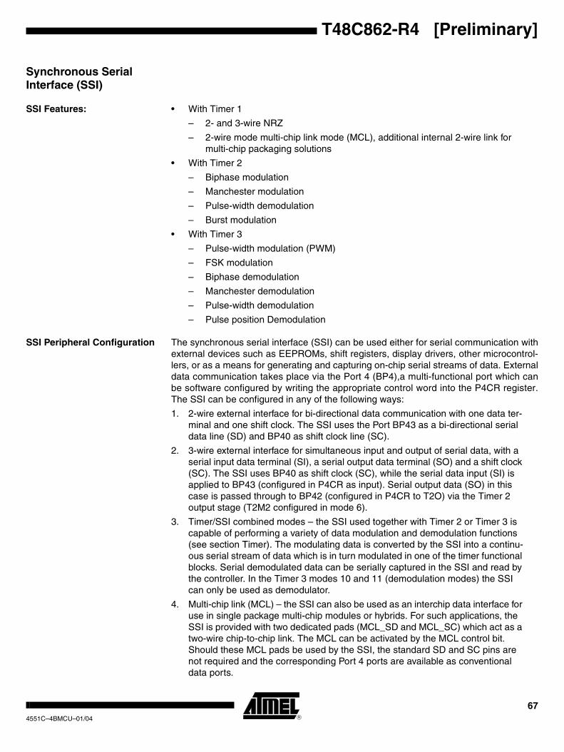
67
T48C862-R4 [Preliminary]
4551C–4BMCU–01/04
Synchronous Serial Interface (SSI)
SSI Features: • With Timer 1
– 2- and 3-wire NRZ
– 2-wire mode multi-chip link mode (MCL), additional internal 2-wire link for multi-chip packaging solutions
• With Timer 2
– Biphase modulation
– Manchester modulation
– Pulse-width demodulation
– Burst modulation
• With Timer 3
– Pulse-width modulation (PWM)
– FSK modulation
– Biphase demodulation
– Manchester demodulation
– Pulse-width demodulation
– Pulse position Demodulation
SSI Peripheral Configuration The synchronous serial interface (SSI) can be used either for serial communication withexternal devices such as EEPROMs, shift registers, display drivers, other microcontrol-lers, or as a means for generating and capturing on-chip serial streams of data. Externaldata communication takes place via the Port 4 (BP4),a multi-functional port which canbe software configured by writing the appropriate control word into the P4CR register.The SSI can be configured in any of the following ways:
1. 2-wire external interface for bi-directional data communication with one data ter-minal and one shift clock. The SSI uses the Port BP43 as a bi-directional serial data line (SD) and BP40 as shift clock line (SC).
2. 3-wire external interface for simultaneous input and output of serial data, with a serial input data terminal (SI), a serial output data terminal (SO) and a shift clock (SC). The SSI uses BP40 as shift clock (SC), while the serial data input (SI) is applied to BP43 (configured in P4CR as input). Serial output data (SO) in this case is passed through to BP42 (configured in P4CR to T2O) via the Timer 2 output stage (T2M2 configured in mode 6).
3. Timer/SSI combined modes – the SSI used together with Timer 2 or Timer 3 is capable of performing a variety of data modulation and demodulation functions (see section Timer). The modulating data is converted by the SSI into a continu-ous serial stream of data which is in turn modulated in one of the timer functional blocks. Serial demodulated data can be serially captured in the SSI and read by the controller. In the Timer 3 modes 10 and 11 (demodulation modes) the SSI can only be used as demodulator.
4. Multi-chip link (MCL) – the SSI can also be used as an interchip data interface for use in single package multi-chip modules or hybrids. For such applications, the SSI is provided with two dedicated pads (MCL_SD and MCL_SC) which act as a two-wire chip-to-chip link. The MCL can be activated by the MCL control bit. Should these MCL pads be used by the SSI, the standard SD and SC pins are not required and the corresponding Port 4 ports are available as conventional data ports.
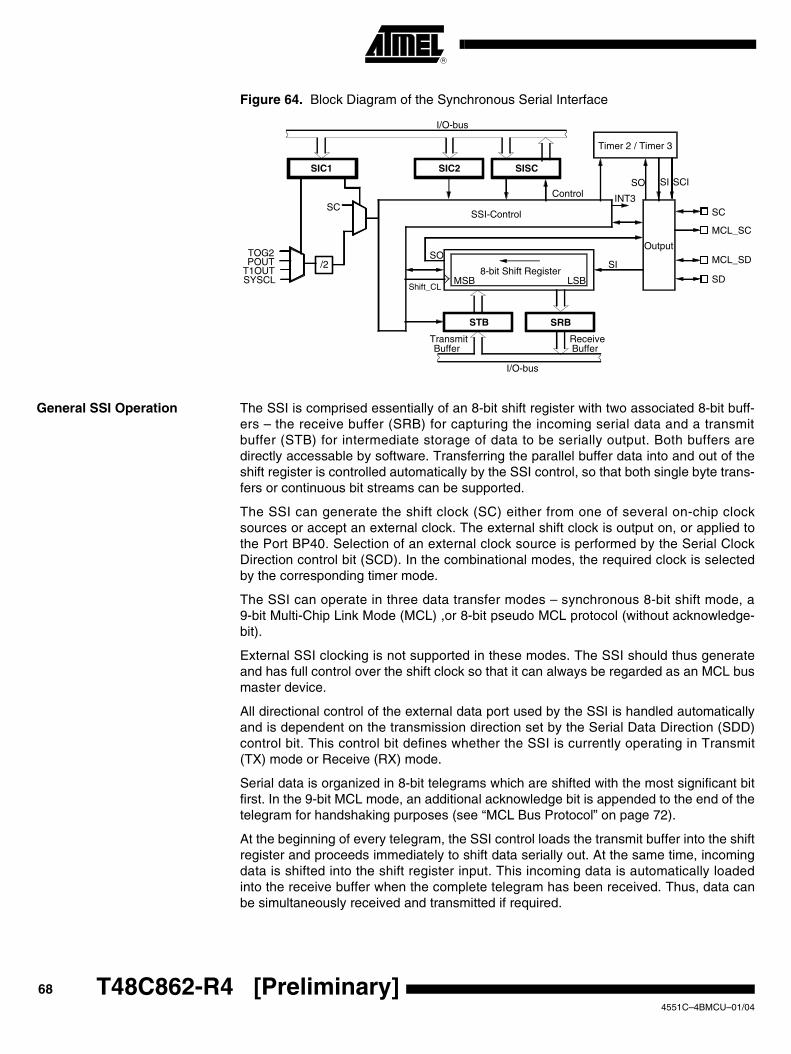
68 T48C862-R4 [Preliminary] 4551C–4BMCU–01/04
Figure 64. Block Diagram of the Synchronous Serial Interface
General SSI Operation The SSI is comprised essentially of an 8-bit shift register with two associated 8-bit buff-ers – the receive buffer (SRB) for capturing the incoming serial data and a transmitbuffer (STB) for intermediate storage of data to be serially output. Both buffers aredirectly accessable by software. Transferring the parallel buffer data into and out of theshift register is controlled automatically by the SSI control, so that both single byte trans-fers or continuous bit streams can be supported.
The SSI can generate the shift clock (SC) either from one of several on-chip clocksources or accept an external clock. The external shift clock is output on, or applied tothe Port BP40. Selection of an external clock source is performed by the Serial ClockDirection control bit (SCD). In the combinational modes, the required clock is selectedby the corresponding timer mode.
The SSI can operate in three data transfer modes – synchronous 8-bit shift mode, a9-bit Multi-Chip Link Mode (MCL) ,or 8-bit pseudo MCL protocol (without acknowledge-bit).
External SSI clocking is not supported in these modes. The SSI should thus generateand has full control over the shift clock so that it can always be regarded as an MCL busmaster device.
All directional control of the external data port used by the SSI is handled automaticallyand is dependent on the transmission direction set by the Serial Data Direction (SDD)control bit. This control bit defines whether the SSI is currently operating in Transmit(TX) mode or Receive (RX) mode.
Serial data is organized in 8-bit telegrams which are shifted with the most significant bitfirst. In the 9-bit MCL mode, an additional acknowledge bit is appended to the end of thetelegram for handshaking purposes (see “MCL Bus Protocol” on page 72).
At the beginning of every telegram, the SSI control loads the transmit buffer into the shiftregister and proceeds immediately to shift data serially out. At the same time, incomingdata is shifted into the shift register input. This incoming data is automatically loadedinto the receive buffer when the complete telegram has been received. Thus, data canbe simultaneously received and transmitted if required.
8-bit Shift RegisterMSB LSB
Shift_CL
SO
SIC1 SIC2 SISC
SCControl
STB SRB
SI
Timer 2 / Timer 3
Output
INT3SC
I/O-bus
I/O-bus
SSI-Control
TOG2POUT
T1OUTSYSCL
SO SI
MCL_SC
SD
MCL_SD
TransmitBuffer
ReceiveBuffer
SCI
/2
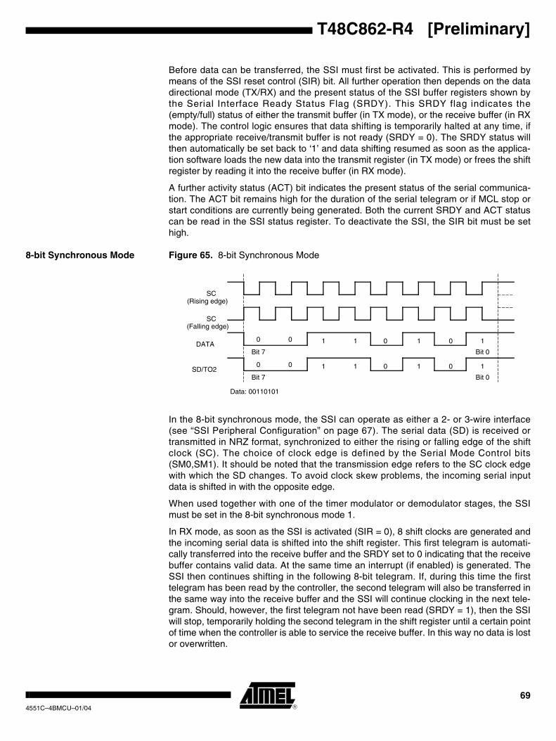
69
T48C862-R4 [Preliminary]
4551C–4BMCU–01/04
Before data can be transferred, the SSI must first be activated. This is performed bymeans of the SSI reset control (SIR) bit. All further operation then depends on the datadirectional mode (TX/RX) and the present status of the SSI buffer registers shown bythe Serial Interface Ready Status Flag (SRDY). This SRDY flag indicates the(empty/full) status of either the transmit buffer (in TX mode), or the receive buffer (in RXmode). The control logic ensures that data shifting is temporarily halted at any time, ifthe appropriate receive/transmit buffer is not ready (SRDY = 0). The SRDY status willthen automatically be set back to ‘1’ and data shifting resumed as soon as the applica-tion software loads the new data into the transmit register (in TX mode) or frees the shiftregister by reading it into the receive buffer (in RX mode).
A further activity status (ACT) bit indicates the present status of the serial communica-tion. The ACT bit remains high for the duration of the serial telegram or if MCL stop orstart conditions are currently being generated. Both the current SRDY and ACT statuscan be read in the SSI status register. To deactivate the SSI, the SIR bit must be sethigh.
8-bit Synchronous Mode Figure 65. 8-bit Synchronous Mode
In the 8-bit synchronous mode, the SSI can operate as either a 2- or 3-wire interface(see “SSI Peripheral Configuration” on page 67). The serial data (SD) is received ortransmitted in NRZ format, synchronized to either the rising or falling edge of the shiftclock (SC). The choice of clock edge is defined by the Serial Mode Control bits(SM0,SM1). It should be noted that the transmission edge refers to the SC clock edgewith which the SD changes. To avoid clock skew problems, the incoming serial inputdata is shifted in with the opposite edge.
When used together with one of the timer modulator or demodulator stages, the SSImust be set in the 8-bit synchronous mode 1.
In RX mode, as soon as the SSI is activated (SIR = 0), 8 shift clocks are generated andthe incoming serial data is shifted into the shift register. This first telegram is automati-cally transferred into the receive buffer and the SRDY set to 0 indicating that the receivebuffer contains valid data. At the same time an interrupt (if enabled) is generated. TheSSI then continues shifting in the following 8-bit telegram. If, during this time the firsttelegram has been read by the controller, the second telegram will also be transferred inthe same way into the receive buffer and the SSI will continue clocking in the next tele-gram. Should, however, the first telegram not have been read (SRDY = 1), then the SSIwill stop, temporarily holding the second telegram in the shift register until a certain pointof time when the controller is able to service the receive buffer. In this way no data is lostor overwritten.
SC
SC
DATA
SD/TO2
1 1 0 1 0 10 0
Bit 7 Bit 0
1 1 0 1 0 10 0
Bit 7 Bit 0
Data: 00110101
(Rising edge)
(Falling edge)
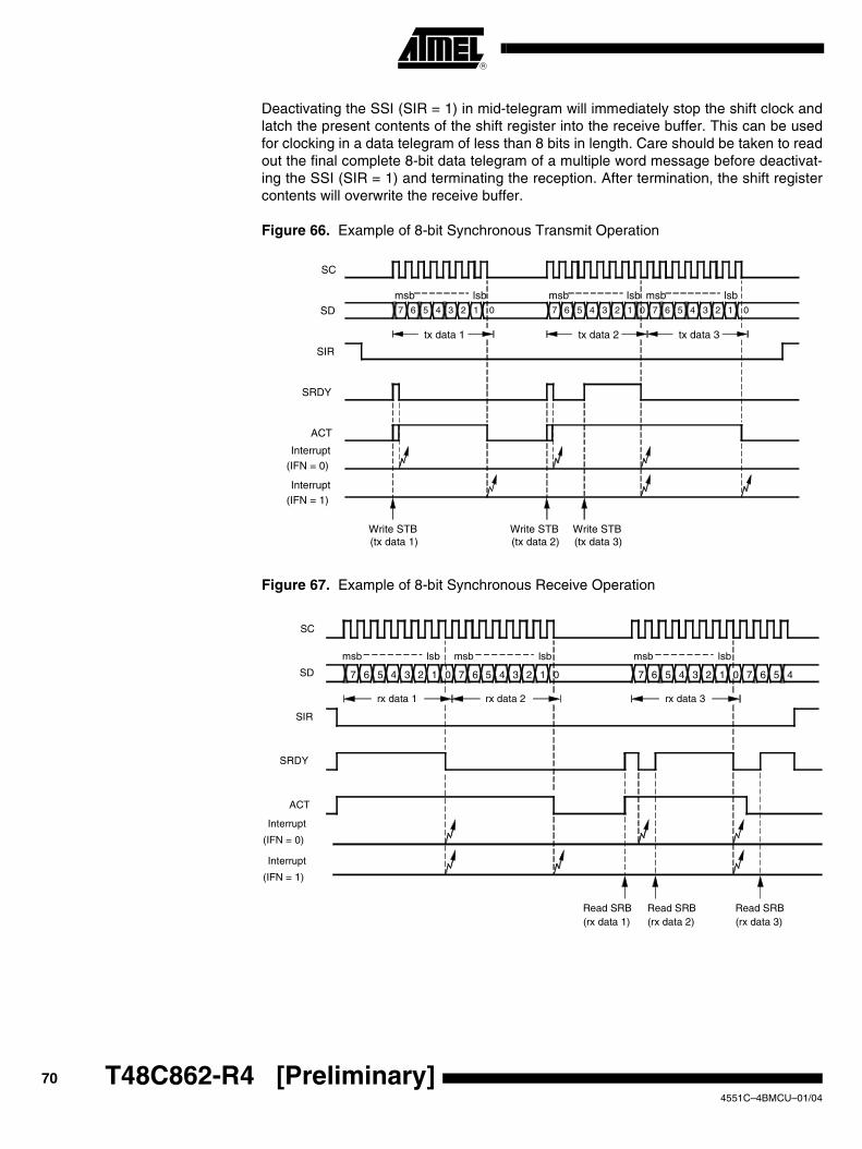
70 T48C862-R4 [Preliminary] 4551C–4BMCU–01/04
Deactivating the SSI (SIR = 1) in mid-telegram will immediately stop the shift clock andlatch the present contents of the shift register into the receive buffer. This can be usedfor clocking in a data telegram of less than 8 bits in length. Care should be taken to readout the final complete 8-bit data telegram of a multiple word message before deactivat-ing the SSI (SIR = 1) and terminating the reception. After termination, the shift registercontents will overwrite the receive buffer.
Figure 66. Example of 8-bit Synchronous Transmit Operation
Figure 67. Example of 8-bit Synchronous Receive Operation
7 6 5 4 3 2 1 0 7 6 5 4 3 2 1 0 7 6 5 4 3 2 1 0
msb lsb
tx data 1 tx data 2 tx data 3
msb lsb msb lsb
Write STB(tx data 2)
Write STB(tx data 3)
Write STB(tx data 1)
SC
SD
SIR
SRDY
Interrupt(IFN = 0)
Interrupt(IFN = 1)
ACT
4 3 2 1 0 7 6 5 4 3 2 1 0
msb lsb
rx data 1 rx data 2 rx data 3
msb lsb msb lsb
Read SRB(rx data 2)
Read SRB(rx data 3)
Read SRB(rx data 1)
SC
SD
SIR
SRDY
Interrupt
(IFN = 0)
Interrupt
(IFN = 1)
ACT
7 6 5 4 3 2 1 07 6 5 7 6 5 4
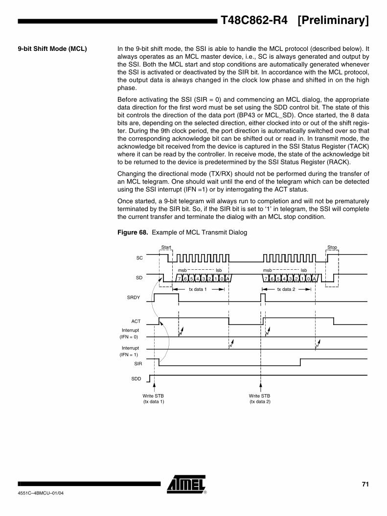
71
T48C862-R4 [Preliminary]
4551C–4BMCU–01/04
9-bit Shift Mode (MCL) In the 9-bit shift mode, the SSI is able to handle the MCL protocol (described below). Italways operates as an MCL master device, i.e., SC is always generated and output bythe SSI. Both the MCL start and stop conditions are automatically generated wheneverthe SSI is activated or deactivated by the SIR bit. In accordance with the MCL protocol,the output data is always changed in the clock low phase and shifted in on the highphase.
Before activating the SSI (SIR = 0) and commencing an MCL dialog, the appropriatedata direction for the first word must be set using the SDD control bit. The state of thisbit controls the direction of the data port (BP43 or MCL_SD). Once started, the 8 databits are, depending on the selected direction, either clocked into or out of the shift regis-ter. During the 9th clock period, the port direction is automatically switched over so thatthe corresponding acknowledge bit can be shifted out or read in. In transmit mode, theacknowledge bit received from the device is captured in the SSI Status Register (TACK)where it can be read by the controller. In receive mode, the state of the acknowledge bitto be returned to the device is predetermined by the SSI Status Register (RACK).
Changing the directional mode (TX/RX) should not be performed during the transfer ofan MCL telegram. One should wait until the end of the telegram which can be detectedusing the SSI interrupt (IFN =1) or by interrogating the ACT status.
Once started, a 9-bit telegram will always run to completion and will not be prematurelyterminated by the SIR bit. So, if the SIR bit is set to ‘1’ in telegram, the SSI will completethe current transfer and terminate the dialog with an MCL stop condition.
Figure 68. Example of MCL Transmit Dialog
7 6 5 4 3 2 1 7 6 5 4 3 2 1 0 A
msb lsb
tx data 1 tx data 2
msb lsb
Write STB(tx data 1)
SC
SD
SRDY
ACT
Interrupt(IFN = 0)
Interrupt(IFN = 1)
0 A
Write STB(tx data 2)
SIR
SDD
Start Stop
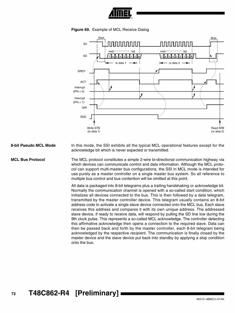
72 T48C862-R4 [Preliminary] 4551C–4BMCU–01/04
Figure 69. Example of MCL Receive Dialog
8-bit Pseudo MCL Mode In this mode, the SSI exhibits all the typical MCL operational features except for theacknowledge bit which is never expected or transmitted.
MCL Bus Protocol The MCL protocol constitutes a simple 2-wire bi-directional communication highway viawhich devices can communicate control and data information. Although the MCL proto-col can support multi-master bus configurations, the SSI in MCL mode is intended foruse purely as a master controller on a single master bus system. So all reference tomultiple bus control and bus contention will be omitted at this point.
All data is packaged into 8-bit telegrams plus a trailing handshaking or acknowledge bit.Normally the communication channel is opened with a so-called start condition, whichinitializes all devices connected to the bus. This is then followed by a data telegram,transmitted by the master controller device. This telegram usually contains an 8-bitaddress code to activate a single slave device connected onto the MCL bus. Each slavereceives this address and compares it with its own unique address. The addressedslave device, if ready to receive data, will respond by pulling the SD line low during the9th clock pulse. This represents a so-called MCL acknowledge. The controller detectingthis affirmative acknowledge then opens a connection to the required slave. Data canthen be passed back and forth by the master controller, each 8-bit telegram beingacknowledged by the respective recipient. The communication is finally closed by themaster device and the slave device put back into standby by applying a stop conditiononto the bus.
7 6 5 4 3 2 1 7 6 5 4 3 2 1 0 A
msb lsb
tx data 1 rx data 2
msb lsb
Write STB(tx data 1)
SC
SD
SRDY
ACT
Interrupt(IFN = 0)
Interrupt(IFN = 1)
0 A
Read SRB(rx data 2)
SIR
SDD
Start Stop
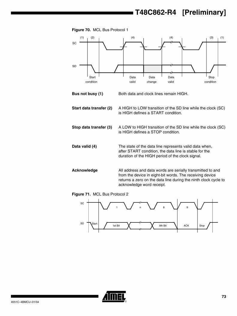
73
T48C862-R4 [Preliminary]
4551C–4BMCU–01/04
Figure 70. MCL Bus Protocol 1
Bus not busy (1) Both data and clock lines remain HIGH.
Start data transfer (2) A HIGH to LOW transition of the SD line while the clock (SC) is HIGH defines a START condition.
Stop data transfer (3) A LOW to HIGH transition of the SD line while the clock (SC)is HIGH defines a STOP condition.
Data valid (4) The state of the data line represents valid data when, after START condition, the data line is stable for the duration of the HIGH period of the clock signal.
Acknowledge All address and data words are serially transmitted to and from the device in eight-bit words. The receiving device returns a zero on the data line during the ninth clock cycle to acknowledge word receipt.
Figure 71. MCL Bus Protocol 2
(2)(1) (4) (4) (3) (1)
Start
condition
Data
valid
Data
change
Data
valid
Stop
condition
SC
SD
SC
SD Start
1 n 8 9
1st Bit 8th Bit ACK Stop

74 T48C862-R4 [Preliminary] 4551C–4BMCU–01/04
SSI Interrupt The SSI interrupt INT3 can be generated either by an SSI buffer register status (i.e.,transmit buffer empty or receive buffer full), the end of SSI data telegram or on the fall-ing edge of the SC/SD pins on Port 4 (see “Port 4 Control Register (P4CR) Byte Write”on page 38). SSI interrupt selection is performed by the Interrupt FunctioN control bit(IFN). The SSI interrupt is usually used to synchronize the software control of the SSIand inform the controller of the present SSI status. The Port 4 interrupts can be usedtogether with the SSI or, if the SSI itself is not required, as additional external interruptsources. In either case this interrupt is capable of waking the controller out of sleepmode.
To enable and select the SSI relevant interrupts use the SSI interrupt mask (SIM) andthe Interrupt Function (IFN) while the Port 4 interrupts are enabled by setting appropri-ate control bits in P4CR register.
Modulation and Demodulation If the shift register is used together with Timer 2 or Timer 3 for modulation or demodula-tion purposes, the 8-bit synchronous mode must be used. In this case, the unused Port4 pins can be used as conventional bi-directional ports.
The modulation and demodulation stages, if enabled, operate as soon as the SSI is acti-vated (SIR = 0) and cease when deactivated (SIR = 1).
Due to the byte-orientated data control, the SSI (when running normally) generatesserial bit streams which are submultiples of 8 bits. An SSI output masking (OMSK) func-tion permits; however, the generation of bit streams of any length. The OMSK signal isderived indirectly from the 4-bit prescaler of the Timer 2 and masks out a programmablenumber of unrequired trailing data bits during the shifting out of the final data word in thebit stream. The number of non-masked data bits is defined by the value pre-pro-grammed in the prescaler compare register. To use output masking, the modulator stopmode bit (MSM) must be set to "0" before programming the final data word into the SSItransmit buffer. This in turn, enables shift clocks to the prescaler when this final word isshifted out. On reaching the compare value, the prescaler triggers the OMSK signal andall following data bits are blanked.
Figure 72. SSI Output Masking Function
8-bit shift registerMSB LSB
Shift_CL
SO
Control
SI
Timer 2
Output
SSI-control
SO
Compare 2/1
4-bit counter 2/1CL2/1
SCL
CM1 OMSK
SC
TOG2POUT
T1OUTSYSCL
/2
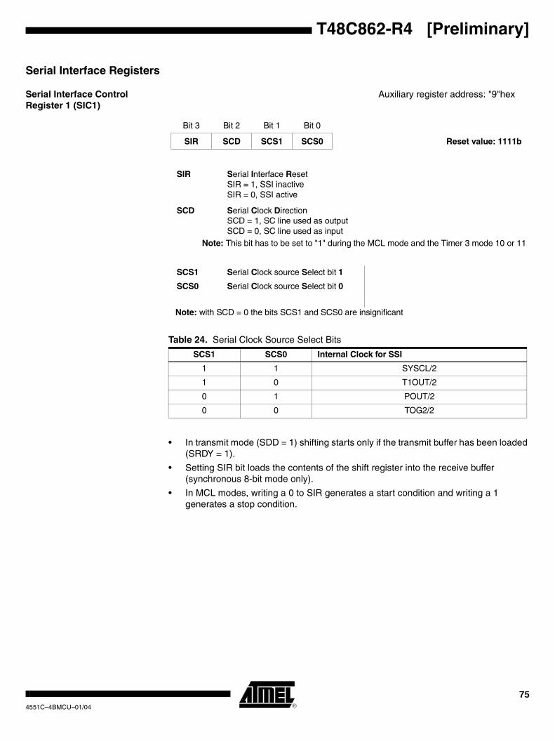
75
T48C862-R4 [Preliminary]
4551C–4BMCU–01/04
Serial Interface Registers
Serial Interface Control Register 1 (SIC1)
Auxiliary register address: "9"hex
Note: This bit has to be set to "1" during the MCL mode and the Timer 3 mode 10 or 11
Note: with SCD = 0 the bits SCS1 and SCS0 are insignificant
Table 24. Serial Clock Source Select Bits
• In transmit mode (SDD = 1) shifting starts only if the transmit buffer has been loaded (SRDY = 1).
• Setting SIR bit loads the contents of the shift register into the receive buffer (synchronous 8-bit mode only).
• In MCL modes, writing a 0 to SIR generates a start condition and writing a 1 generates a stop condition.
Bit 3 Bit 2 Bit 1 Bit 0
SIR SCD SCS1 SCS0 Reset value: 1111b
SIR Serial Interface ResetSIR = 1, SSI inactiveSIR = 0, SSI active
SCD Serial Clock DirectionSCD = 1, SC line used as outputSCD = 0, SC line used as input
SCS1 Serial Clock source Select bit 1
SCS0 Serial Clock source Select bit 0
SCS1 SCS0 Internal Clock for SSI
1 1 SYSCL/2
1 0 T1OUT/2
0 1 POUT/2
0 0 TOG2/2
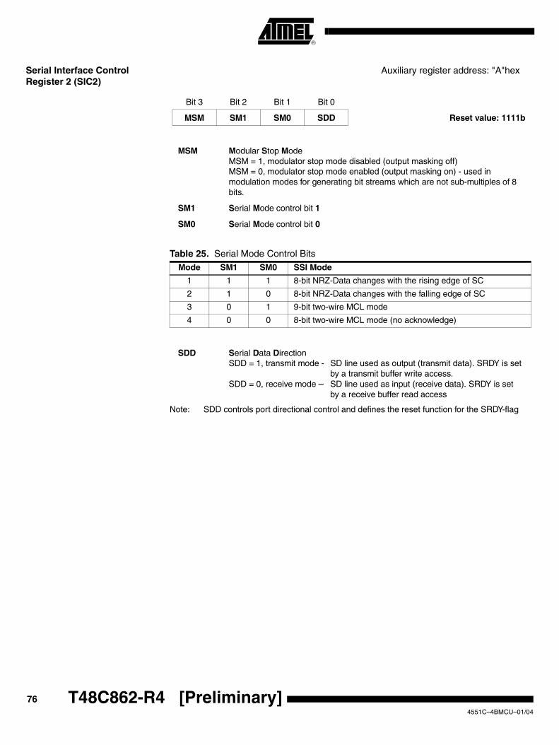
76 T48C862-R4 [Preliminary] 4551C–4BMCU–01/04
Serial Interface Control Register 2 (SIC2)
Auxiliary register address: "A"hex
Table 25. Serial Mode Control Bits
Note: SDD controls port directional control and defines the reset function for the SRDY-flag
Bit 3 Bit 2 Bit 1 Bit 0
MSM SM1 SM0 SDD Reset value: 1111b
MSM Modular Stop ModeMSM = 1, modulator stop mode disabled (output masking off)MSM = 0, modulator stop mode enabled (output masking on) - used in modulation modes for generating bit streams which are not sub-multiples of 8 bits.
SM1 Serial Mode control bit 1
SM0 Serial Mode control bit 0
Mode SM1 SM0 SSI Mode
1 1 1 8-bit NRZ-Data changes with the rising edge of SC
2 1 0 8-bit NRZ-Data changes with the falling edge of SC
3 0 1 9-bit two-wire MCL mode
4 0 0 8-bit two-wire MCL mode (no acknowledge)
SDD Serial Data DirectionSDD = 1, transmit mode - SD line used as output (transmit data). SRDY is set
by a transmit buffer write access.SDD = 0, receive mode – SD line used as input (receive data). SRDY is set
by a receive buffer read access

77
T48C862-R4 [Preliminary]
4551C–4BMCU–01/04
Serial Interface Status and Control Register (SISC)
Primary register address: "A"hex
Serial Transmit Buffer (STB) – Byte Write
Primary register address: "9"hex
The STB is the transmit buffer of the SSI. The SSI transfers the transmit buffer into the shift regis-ter and starts shifting with the most significant bit.
Bit 3 Bit 2 Bit 1 Bit 0
Write MCL RACK SIM IFN Reset value: 1111b
Read – TACK ACT SRDY Reset value: xxxxb
MCL Multi-Chip Link activationMCL = 1,multi-chip link disabled. This bit has to be set to "0" during
transactions to/from the internal EEPROM MCL = 0, connects SC and SD additionally to the internal multi-chip link pads
RACK Receive ACKnowledge status/control bit for MCL modeRACK = 0, transmit acknowledge in next receive telegramRACK = 1, transmit no acknowledge in last receive telegram
TACK Transmit ACKnowledge status/control bit for MCL modeTACK = 0, acknowledge received in last transmit telegramTACK = 1, no acknowledge received in last transmit telegram
SIM Serial Interrupt MaskSIM = 1, disable interruptsSIM = 0, enable serial interrupt. An interrupt is generated.
IFN Interrupt FuNctionIFN = 1, the serial interrupt is generated at the end of telegramIFN = 0, the serial interrupt is generated when the SRDY goes low (i.e., buffer
becomes empty/full in transmit/receive mode)
SRDY Serial interface buffer ReaDY status flagSRDY = 1, in receive mode: receive buffer empty
in transmit mode: transmit buffer full SRDY = 0, in receive mode: receive buffer full
in transmit mode: transmit buffer empty
ACT Transmission ACTive status flagACT = 1, transmission is active, i.e., serial data transfer. Stop or start conditions
are currently in progress.ACT = 0, transmission is inactive
First write cycle Bit 3 Bit 2 Bit 1 Bit 0 Reset value: xxxxb
Second write cycle Bit 7 Bit 6 Bit 5 Bit 4 Reset value: xxxxb

78 T48C862-R4 [Preliminary] 4551C–4BMCU–01/04
Serial Receive Buffer (SRB) – Byte Read
Primary register address: "9"hex
The SRB is the receive buffer of the SSI. The shift register clocks serial data in (most significantbit first) and loads content into the receive buffer when complete telegram has been received.
Combination Modes The UTCM consists of two timers (Timer 2 and Timer 3) and a serial interface. There isa multitude of modes in which the timers and serial interface can work together.
The 8-bit wide serial interface operates as shift register for modulation and demodula-tion. The modulator and demodulator units work together with the timers and shift thedata bits into or out of the shift register.
Combination Mode Timer 2 and SSI
Figure 73. Combination Timer 2 and SSI
First read cycle Bit 7 Bit 6 Bit 5 Bit 4 Reset value: xxxxb
Second read cycle Bit 3 Bit 2 Bit 1 Bit 0 Reset value: xxxxb
4-bit counter 2/1
RES OVF1
Compare 2/1
T2CO1
POUT
CL2/2DCG
T2M1P4CR
8-bit counter 2/2
RES OVF2
Compare 2/2
T2CO2T2CM
Timer 2 - controlTOG2
INT4Biphase-,
Manchester-modulator
Output
MOUT
T2O
Timer 2modulator
output-stage
T2M2
SO Control
T2C
CL2/1
T2I
SYSCLT1OUT
TOG3SCL
I/O-bus
8-bit shift registerMSB LSB
Shift_CL
SO
SIC1 SIC2 SISC
SCLI
Control
STB SRB
SI
Output
INT3
I/O-bus
SSI-control
TOG2
POUTT1OUTSYSCL MCL_SC
MCL_SD
Transmitbuffer
Receivebuffer
CM1
I/O-bus
POUT
SO
SCL
SC
SD
DCGO
TOG2
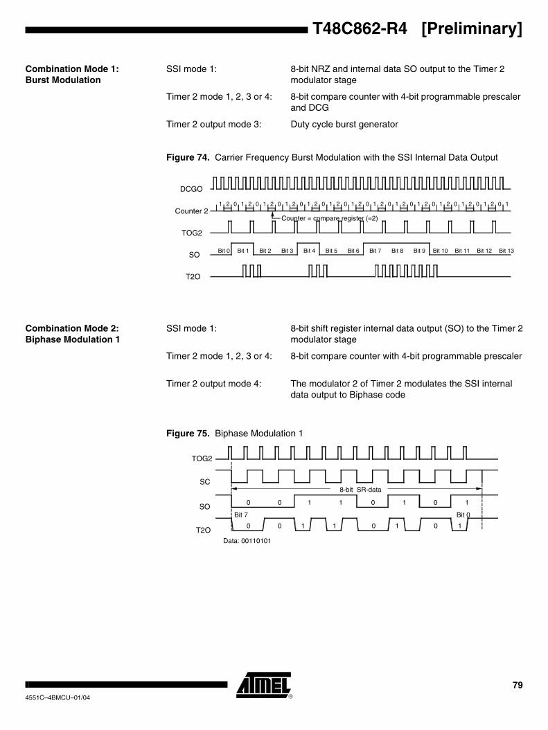
79
T48C862-R4 [Preliminary]
4551C–4BMCU–01/04
Combination Mode 1:Burst Modulation
SSI mode 1: 8-bit NRZ and internal data SO output to the Timer 2 modulator stage
Timer 2 mode 1, 2, 3 or 4: 8-bit compare counter with 4-bit programmable prescaler and DCG
Timer 2 output mode 3: Duty cycle burst generator
Figure 74. Carrier Frequency Burst Modulation with the SSI Internal Data Output
Combination Mode 2: Biphase Modulation 1
SSI mode 1: 8-bit shift register internal data output (SO) to the Timer 2modulator stage
Timer 2 mode 1, 2, 3 or 4: 8-bit compare counter with 4-bit programmable prescaler
Timer 2 output mode 4: The modulator 2 of Timer 2 modulates the SSI internal data output to Biphase code
Figure 75. Biphase Modulation 1
1 2 0 1 2 0 1 2 0 1 2 0 1 2 0 1 2 0 1 2 0 1 2 0 1 2 0 1 2 0 1 2 0 1 2 0 1 2 0 1
DCGO
Counter 2
TOG2
SO
T2O
Counter = compare register (=2)
Bit 0 Bit 1 Bit 2 Bit 3 Bit 4 Bit 5 Bit 6 Bit 7 Bit 8 Bit 9 Bit 10 Bit 11 Bit 12 Bit 13
TOG2
SC
SO
T2O0 0 00
0 0 1 1 0 1 0 1
1 1 1 1
8-bit SR-data
Bit 7 Bit 0
Data: 00110101

80 T48C862-R4 [Preliminary] 4551C–4BMCU–01/04
Combination Mode 3: Manchester Modulation 1
SSI mode 1: 8-bit shift register internal data output (SO) to the Timer 2modulator stage
Timer 2 mode 1, 2, 3 or 4: 8-bit compare counter with 4-bit programmable prescaler
Timer 2 output mode 5: The modulator 2 of Timer 2 modulates the SSI internal data output to Manchester code
Figure 76. Manchester Modulation 1
Combination Mode 4: Manchester Modulation 2
SSI mode 1: 8-bit shift register internal data output (SO) to the Timer 2 modulator stage
Timer 2 mode 3: 8-bit compare counter and 4-bit prescaler
Timer 2 output mode 5: The modulator 2 of Timer 2 modulates the SSI data output to Manchester code
The 4-bit stage can be used as prescaler for the SSI to generate the stop signal for mod-ulator 2. The SSI has a special mode to supply the prescaler with the shift clock.The control output signal (OMSK) of the SSI is used as stop signal for the modulator.Figure 77 on page 80 shows an example for a 12-bit Manchester telegram.
Figure 77. Manchester Modulation 2
TOG2
SC
SO
T2O0 00
0 0 1 1 0 1 0 1
1 1 1 1
8-bit SR-data
Bit 7 Bit 0
0
Bit 7 Bit 0
Data: 00110101
0 0 0 0 0 0 0 0 1 2 3 4 0 1 20Counter 2/1 = Compare Register 2/1 (= 4)
Bit 7 Bit 6 Bit 5 Bit 4 Bit 3 Bit 2 Bit 1 Bit 0 Bit 7 Bit 6 Bit 5 Bit 4 Bit 3 Bit 2 Bit 1 Bit 0
SCLI
Buffer full
SIR
SO
SC
MSM
Timer 2Mode 3
SCL
Counter 2/1
OMSK
T2O
3
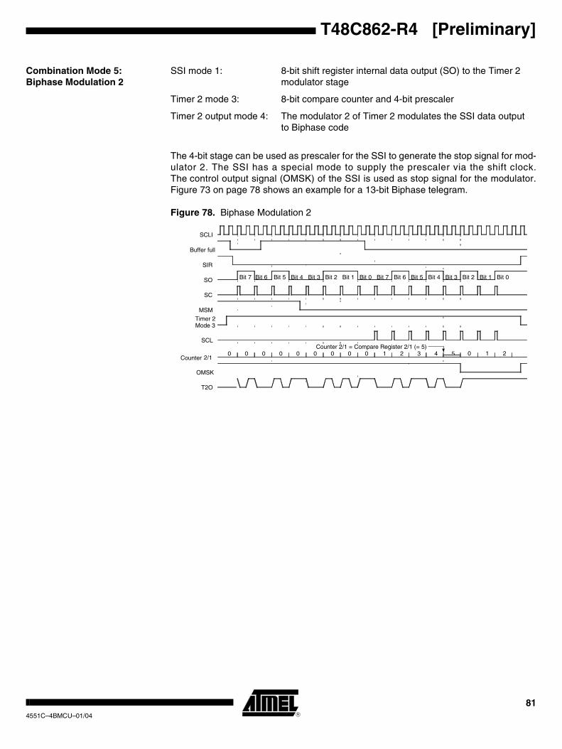
81
T48C862-R4 [Preliminary]
4551C–4BMCU–01/04
Combination Mode 5: Biphase Modulation 2
SSI mode 1: 8-bit shift register internal data output (SO) to the Timer 2modulator stage
Timer 2 mode 3: 8-bit compare counter and 4-bit prescaler
Timer 2 output mode 4: The modulator 2 of Timer 2 modulates the SSI data output to Biphase code
The 4-bit stage can be used as prescaler for the SSI to generate the stop signal for mod-ulator 2. The SSI has a special mode to supply the prescaler via the shift clock.The control output signal (OMSK) of the SSI is used as stop signal for the modulator.Figure 73 on page 78 shows an example for a 13-bit Biphase telegram.
Figure 78. Biphase Modulation 2
0 0 0 0 0 0 0 0 1 2 3 4 50Counter 2/1 = Compare Register 2/1 (= 5)
Bit 7 Bit 6 Bit 5 Bit 4 Bit 3 Bit 2 Bit 1 Bit 0 Bit 7 Bit 6 Bit 5 Bit 4 Bit 3 Bit 2 Bit 1 Bit 0
SCLI
Buffer full
SIR
SO
SC
MSMTimer 2Mode 3
SCL
Counter 2/1
OMSK
T2O
0 1 2

82 T48C862-R4 [Preliminary] 4551C–4BMCU–01/04
Combination Mode Timer 3 and SSI
Figure 79. Combination Timer 3 and SSI
Combination Mode 6:FSK Modulation
SSI mode 1: 8-bit shift register internal data output (SO) to the Timer 3
Timer 3 mode 8: FSK modulation with shift register data (SO)
The two compare registers are used to generate two varied time intervals. The SSI dataoutput selects which compare register is used for the output frequency generation. A "0"level at the SSI data output enables the compare register 1 and a "1" level enables thecompare register 2. The compare and compare mode registers must be programmed togenerate the two frequencies via the output toggle flip-lop. The SSI can be supplied withthe toggle signal of Timer 2 or any other clock source. The Timer 3 counter is driven byan internal or external clock source.
Figure 80. FSK Modulation
8-bit counter 3
RES
Compare 3/1
T3CO1
T3CP
T3CO2
Timer 3 - control
T3O
CL3
T3I
T3EXSYSCLT1OUT
POUT
I/O-bus
Compare 3/2
T3CM1 T3CM2
T3C T3ST
Modulator 3
Demodu-lator 3
M2
ControlSO
TOG3
INT5
RES
CM31
T3I
T3EX
SI
SC
T3MT3CS
CP3
8-bit shift registerMSB LSB
Shift_CL
SO
SIC1 SIC2 SISC
SCLI
Control
STB SRB
SI
Output
INT3
I/O-bus
SSI-control
TOG2POUT
T1OUTSYSCL
SI
MCL_SC
MCL_SD
Transmit buffer Receive buffer
SC
SC
SI
0 1 2 3 4 0 1 2 3 4 0 1 2 0Counter 3
CM31
CM32
SO
1 2 0 1 2 0 1 2 0 1 2 0 1 2 0 1 2 0 1 2 0 1 2 3 4 0
T3R
1 2
T3O
3
0 1 0
4 0
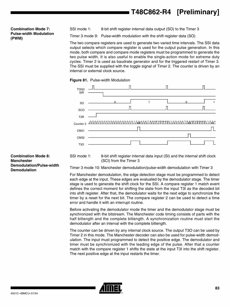
83
T48C862-R4 [Preliminary]
4551C–4BMCU–01/04
Combination Mode 7: Pulse-width Modulation (PWM)
SSI mode 1: 8-bit shift register internal data output (SO) to the Timer 3
Timer 3 mode 9: Pulse-width modulation with the shift register data (SO)
The two compare registers are used to generate two varied time intervals. The SSI dataoutput selects which compare register is used for the output pulse generation. In thismode, both compare and compare mode registers must be programmed to generate thetwo pulse width. It is also useful to enable the single-action mode for extreme dutycycles. Timer 2 is used as baudrate generator and for the triggered restart of Timer 3.The SSI must be supplied with the toggle signal of Timer 2. The counter is driven by aninternal or external clock source.
Figure 81. Pulse-width Modulation
Combination Mode 8: Manchester Demodulation/Pulse-width Demodulation
SSI mode 1: 8-bit shift register internal data input (SI) and the internal shift clock(SCI) from the Timer 3
Timer 3 mode 10: Manchester demodulation/pulse-width demodulation with Timer 3
For Manchester demodulation, the edge detection stage must be programmed to detecteach edge at the input. These edges are evaluated by the demodulator stage. The timerstage is used to generate the shift clock for the SSI. A compare register 1 match eventdefines the correct moment for shifting the state from the input T3I as the decoded bitinto shift register. After that, the demodulator waits for the next edge to synchronize thetimer by a reset for the next bit. The compare register 2 can be used to detect a timeerror and handle it with an interrupt routine.
Before activating the demodulator mode the timer and the demodulator stage must besynchronized with the bitstream. The Manchester code timing consists of parts with thehalf bitlength and the complete bitlength. A synchronization routine must start thedemodulator after an interval with the complete bitlength.
The counter can be driven by any internal clock source. The output T3O can be used byTimer 2 in this mode. The Manchester decoder can also be used for pulse-width demod-ulation. The input must programmed to detect the positive edge. The demodulator andtimer must be synchronized with the leading edge of the pulse. After that a countermatch with the compare register 1 shifts the state at the input T3I into the shift register.The next positive edge at the input restarts the timer.
0 0 0 0 0 0 0 0 0 0 0 0 0Counter 3
CM31
CM32
T3O
0 0 0 0 0 1 2 3 4 5 6 7 8 9 1011121314150 1 2 3 4 5
TOG2
6 7 8
1
9 111210 1413 0 2 31 4150
00 1
SIR
SO
SCO
T3R
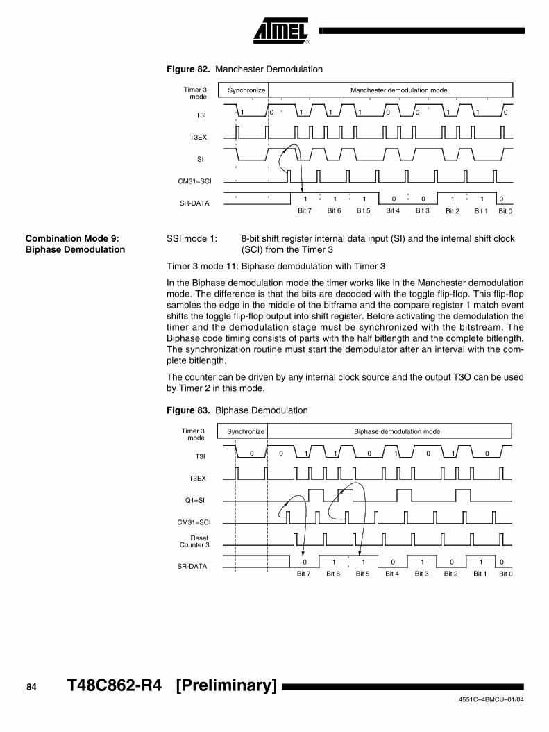
84 T48C862-R4 [Preliminary] 4551C–4BMCU–01/04
Figure 82. Manchester Demodulation
Combination Mode 9: Biphase Demodulation
SSI mode 1: 8-bit shift register internal data input (SI) and the internal shift clock(SCI) from the Timer 3
Timer 3 mode 11: Biphase demodulation with Timer 3
In the Biphase demodulation mode the timer works like in the Manchester demodulationmode. The difference is that the bits are decoded with the toggle flip-flop. This flip-flopsamples the edge in the middle of the bitframe and the compare register 1 match eventshifts the toggle flip-flop output into shift register. Before activating the demodulation thetimer and the demodulation stage must be synchronized with the bitstream. TheBiphase code timing consists of parts with the half bitlength and the complete bitlength.The synchronization routine must start the demodulator after an interval with the com-plete bitlength.
The counter can be driven by any internal clock source and the output T3O can be usedby Timer 2 in this mode.
Figure 83. Biphase Demodulation
1 0 1 1 1 0 0 1 1 0
1 1
Bit 7 Bit 6 Bit 5 Bit 4 Bit 3 Bit 2 Bit 1
Synchronize Manchester demodulation modeTimer 3mode
T3EX
SI
SR-DATA
T3I
CM31=SCI
1 0 0 1 1 0
Bit 0
0 1 1 1 1
0 1
Bit 7 Bit 6 Bit 5 Bit 4 Bit 3 Bit 2 Bit 1
Synchronize Biphase demodulation modeTimer 3mode
T3EX
Q1=SI
CM31=SCI
SR-DATA
0 0 0 0T3I
ResetCounter 3
1 0 1 0 1 0
Bit 0

85
T48C862-R4 [Preliminary]
4551C–4BMCU–01/04
Combination Mode Timer 2 and Timer 3
Figure 84. Combination Timer 3 and Timer 2
Combination Mode 10: Frequency Measurement or Event Counter with Time Gate
Timer 2 mode 1/2: 12-bit compare counter/8-bit compare counter and 4-bit prescaler
Timer 2 output mode 1/6: Timer 2 compare match toggles (TOG2) to the Timer 3
Timer 3 mode 3: Timer/Counter; internal trigger restart and internal capture(with Timer 2 TOG2-signal)
The counter is driven by an external (T3I) clock source. The output signal (TOG2) ofTimer 2 resets the counter. The counter value before reset is saved in the capture regis-ter. If single-action mode is activated for one or both compare registers, the triggersignal restarts also the single actions. This mode can be used for frequency measure-ments or as event counter with time gate.
8-bit counter 3
RES
Compare 3/1
T3CO1
T3CP
T3CO2
Timer 3 - control
T3O
CL3
T3I
T3EXSYSCLT1OUT
POUT
I/O-bus
Compare 3/2
T3CM1 T3CM2
T3C T3ST
Modulator 3
Demodu-lator 3
ControlSO
TOG3
INT5
RES
CM31
T3I
T3EX
TOG2
SI
SCI
SSI
CP3
4-bit counter 2/1
RES OVF1
Compare 2/1
T2CO1
CM1
POUT
SSI
CL2/2DCG
T2M1P4CR
8-bit counter 2/2
RES OVF2
Compare 2/2
T2CO2T2CM
TOG2
INT4Biphase-,
Manchester-modulator
OUTPUT
MOUT
M2
T2O
Timer 2modulator 2output-stage
T2M2
Control(RE, FE, SCO, OMSK)SSI
T2C
CL2/1TOG3
SYSCLT1OUT
SCL
Timer 2 - control
M2
T3CS T3M
POUT
DCGO
SO
T2I
I/O-bus
I/O-bus
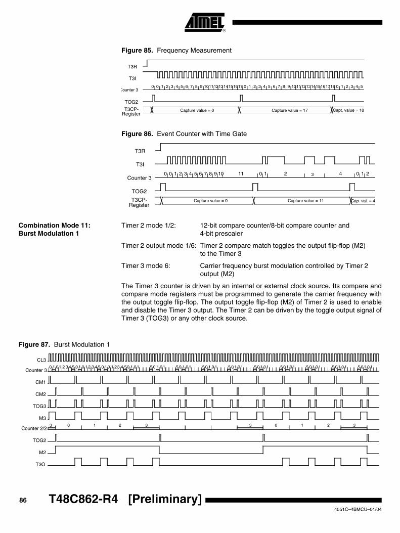
86 T48C862-R4 [Preliminary] 4551C–4BMCU–01/04
Figure 85. Frequency Measurement
Figure 86. Event Counter with Time Gate
Combination Mode 11: Burst Modulation 1
Timer 2 mode 1/2: 12-bit compare counter/8-bit compare counter and 4-bit prescaler
Timer 2 output mode 1/6: Timer 2 compare match toggles the output flip-flop (M2) to the Timer 3
Timer 3 mode 6: Carrier frequency burst modulation controlled by Timer 2 output (M2)
The Timer 3 counter is driven by an internal or external clock source. Its compare andcompare mode registers must be programmed to generate the carrier frequency withthe output toggle flip-flop. The output toggle flip-flop (M2) of Timer 2 is used to enableand disable the Timer 3 output. The Timer 2 can be driven by the toggle output signal ofTimer 3 (TOG3) or any other clock source.
Figure 87. Burst Modulation 1
0 0 1 2 3 4 5 6 7 8 9 10Counter 3
TOG2
T3CP-Register
T3I
T3R
Capture value = 0 Capture value = 17 Capt. value = 18
11121314151617 1 2 3 4 5 6 7 8 9 1011121314151617180 0 1 2 3 4 5
0 0 1 2 3 4 5 6 7 8 9 10Counter 3
TOG2
T3CP-Register
11 0 1 2 4 0 1
T3I
23
T3R
Capture value = 0 Capture value = 11 Cap. val. = 4
0 1 01 2 3 4 5 0 1 0 12 3 4 5 0 10 1 23 4 50 1 01 5 0 1 0 1 5 0 1 0 1 5 0 1 0 1 5 0 1 01 5 0 1 0 1 5 0 1 01 5 0 1 01 5 0 1 0 1 5 01 0 1
3 0 1 2 3 3 0 1 32
CL3
Counter 3
CM1
CM2
TOG3
M3
Counter 2/2
TOG2
M2
T3O

87
T48C862-R4 [Preliminary]
4551C–4BMCU–01/04
Combination Mode Timer 2, Timer 3 and SSI
Figure 88. Combination Timer 2, Timer 3 and SSI
8-bit Counter 3
RES
Compare 3/1
T3CO1
T3CP
T3CO2
Timer 3 - control
T3O
CL3
T3I
T3EXSYSCLT1OUT
POUT
I/O-bus
Compare 3/2
T3CM1 T3CM2
T3C T3ST
Modulator 3
Demodu-lator 3
Control
SOTOG3
INT5
RES
CM31
T3I
T3EX
TOG2
SI
SCI
SSI
CP3
4-bit Counter 2/1
RES OVF1
Compare 2/1
T2CO1
CM1
POUT
CL2/2 DCG
T2M1P4CR
8-bit Counter 2/2
RES OVF2
Compare 2/2
T2CO2T2CM
TOG2
INT4Biphase-,
Manchester-modulator
OUTPUT
MOUT
M2
T2O
Timer 2modulator 2output-stage
T2M2
Control
(RE, FE,SCO, OMSK)
T2C
CL2/1TOG3
SYSCLT1OUT
SCL
Timer 2 - control
M2
T3CS T3M
POUT
DCGO
SO
T2I
I/O-bus
I/O-bus
8-bit shift registerMSB LSBShift_CL
SO
SIC1 SIC2 SISC
SCLI
Control
STB SRB
SI
Output
INT3
I/O-bus
SSI-control
TOG2
POUTT1OUTSYSCL MCL_SC
MCL_SD
Transmit buffer Receive buffer
SC
SISCL
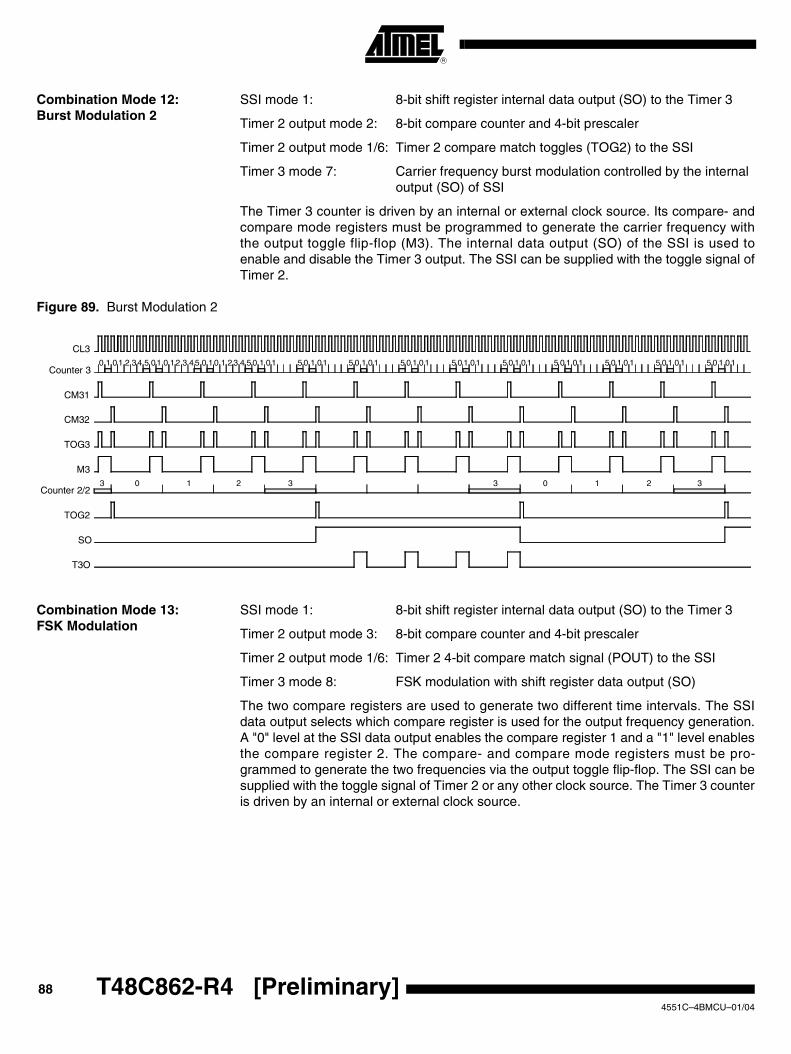
88 T48C862-R4 [Preliminary] 4551C–4BMCU–01/04
Combination Mode 12: Burst Modulation 2
SSI mode 1: 8-bit shift register internal data output (SO) to the Timer 3
Timer 2 output mode 2: 8-bit compare counter and 4-bit prescaler
Timer 2 output mode 1/6: Timer 2 compare match toggles (TOG2) to the SSI
Timer 3 mode 7: Carrier frequency burst modulation controlled by the internaloutput (SO) of SSI
The Timer 3 counter is driven by an internal or external clock source. Its compare- andcompare mode registers must be programmed to generate the carrier frequency withthe output toggle flip-flop (M3). The internal data output (SO) of the SSI is used toenable and disable the Timer 3 output. The SSI can be supplied with the toggle signal ofTimer 2.
Figure 89. Burst Modulation 2
Combination Mode 13: FSK Modulation
SSI mode 1: 8-bit shift register internal data output (SO) to the Timer 3
Timer 2 output mode 3: 8-bit compare counter and 4-bit prescaler
Timer 2 output mode 1/6: Timer 2 4-bit compare match signal (POUT) to the SSI
Timer 3 mode 8: FSK modulation with shift register data output (SO)
The two compare registers are used to generate two different time intervals. The SSIdata output selects which compare register is used for the output frequency generation.A "0" level at the SSI data output enables the compare register 1 and a "1" level enablesthe compare register 2. The compare- and compare mode registers must be pro-grammed to generate the two frequencies via the output toggle flip-flop. The SSI can besupplied with the toggle signal of Timer 2 or any other clock source. The Timer 3 counteris driven by an internal or external clock source.
0 1 01 2 34 5 01 0 12 3 45 0 10 1 23 4 5 0 1 01 5 0 1 01 5 0 1 01 5 0 1 01 5 0 1 01 5 0 1 0 1 5 0 1 01 5 0 1 0 1 5 0 1 0 1 5 0 1 01
3 0 1 2 3 3 0 1 32
CL3
Counter 3
CM31
CM32
TOG3
M3
Counter 2/2
TOG2
SO
T3O
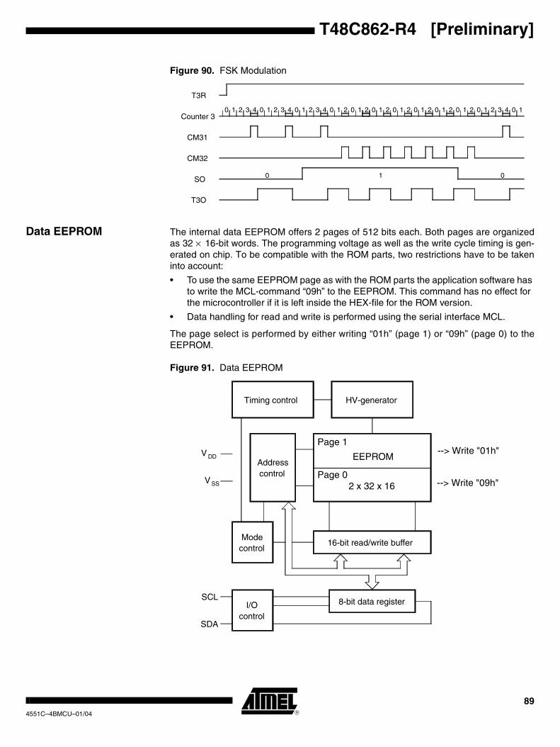
89
T48C862-R4 [Preliminary]
4551C–4BMCU–01/04
Figure 90. FSK Modulation
Data EEPROM The internal data EEPROM offers 2 pages of 512 bits each. Both pages are organizedas 32 × 16-bit words. The programming voltage as well as the write cycle timing is gen-erated on chip. To be compatible with the ROM parts, two restrictions have to be takeninto account:
• To use the same EEPROM page as with the ROM parts the application software has to write the MCL-command “09h” to the EEPROM. This command has no effect for the microcontroller if it is left inside the HEX-file for the ROM version.
• Data handling for read and write is performed using the serial interface MCL.
The page select is performed by either writing “01h” (page 1) or “09h” (page 0) to theEEPROM.
Figure 91. Data EEPROM
0 1 2 3 4 0 1 2 3 4 0 1 2 3Counter 3
CM31
CM32
SO
4 0 1 2 0 1 2 0 1 2 0 1 2 0 1 2 0 1 2 0 1 2 0 1 2 3
T3R
4 0
T3O
1
0 1 0
16-bit read/write buffer
Addresscontrol
8-bit data register
EEPROM
2 x 32 x 16
HV-generatorTiming control
Modecontrol
I/Ocontrol
SCL
V DD
V SS
SDA
Page 1
Page 0
--> Write "01h"
--> Write "09h"
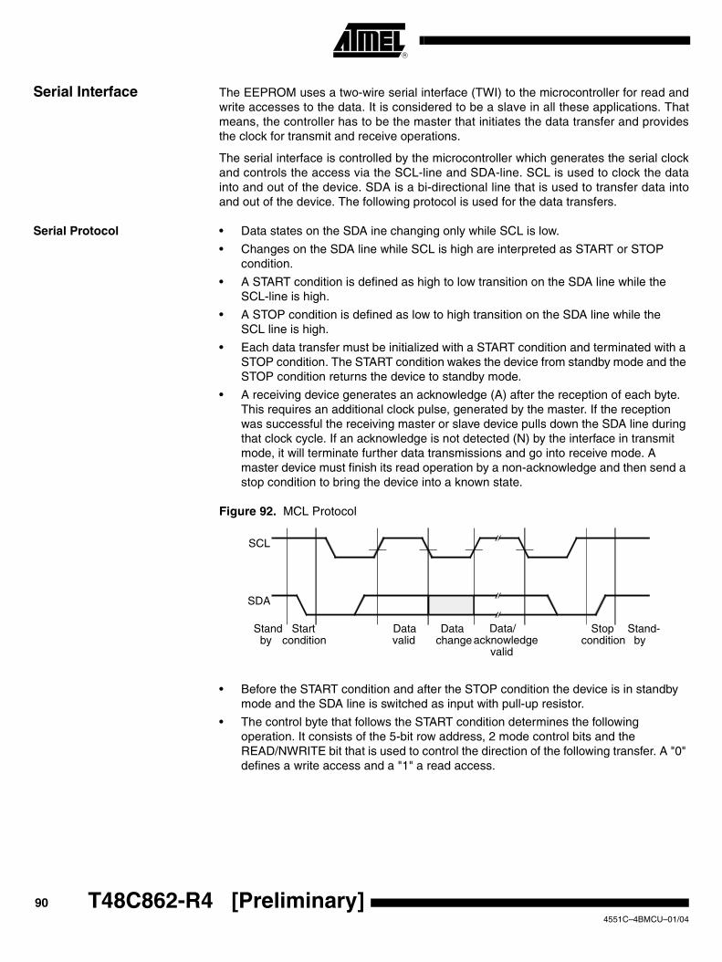
90 T48C862-R4 [Preliminary] 4551C–4BMCU–01/04
Serial Interface The EEPROM uses a two-wire serial interface (TWI) to the microcontroller for read andwrite accesses to the data. It is considered to be a slave in all these applications. Thatmeans, the controller has to be the master that initiates the data transfer and providesthe clock for transmit and receive operations.
The serial interface is controlled by the microcontroller which generates the serial clockand controls the access via the SCL-line and SDA-line. SCL is used to clock the datainto and out of the device. SDA is a bi-directional line that is used to transfer data intoand out of the device. The following protocol is used for the data transfers.
Serial Protocol • Data states on the SDA ine changing only while SCL is low.
• Changes on the SDA line while SCL is high are interpreted as START or STOP condition.
• A START condition is defined as high to low transition on the SDA line while the SCL-line is high.
• A STOP condition is defined as low to high transition on the SDA line while the SCL line is high.
• Each data transfer must be initialized with a START condition and terminated with a STOP condition. The START condition wakes the device from standby mode and the STOP condition returns the device to standby mode.
• A receiving device generates an acknowledge (A) after the reception of each byte. This requires an additional clock pulse, generated by the master. If the reception was successful the receiving master or slave device pulls down the SDA line during that clock cycle. If an acknowledge is not detected (N) by the interface in transmit mode, it will terminate further data transmissions and go into receive mode. A master device must finish its read operation by a non-acknowledge and then send a stop condition to bring the device into a known state.
Figure 92. MCL Protocol
• Before the START condition and after the STOP condition the device is in standby mode and the SDA line is switched as input with pull-up resistor.
• The control byte that follows the START condition determines the following operation. It consists of the 5-bit row address, 2 mode control bits and the READ/NWRITE bit that is used to control the direction of the following transfer. A "0" defines a write access and a "1" a read access.
Startcondition
Datavalid
Datachange
Data/acknowledge
valid
Stopcondition
SCL
SDA
Standby
Stand-by
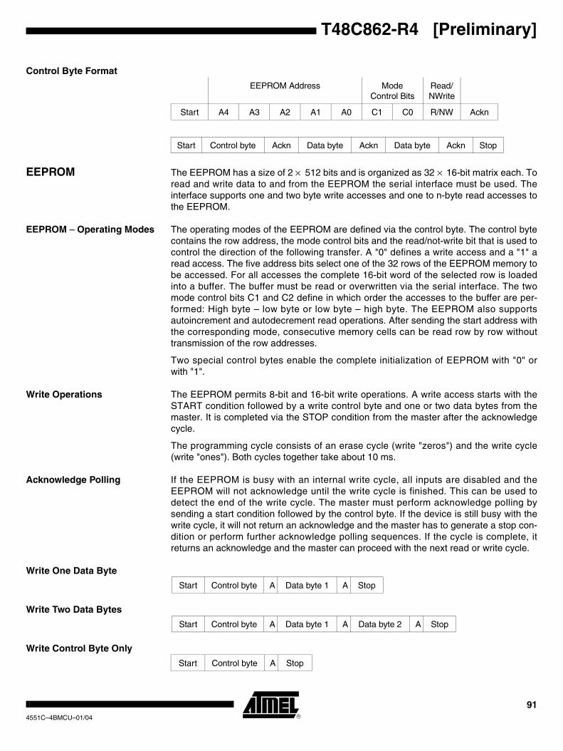
91
T48C862-R4 [Preliminary]
4551C–4BMCU–01/04
Control Byte Format
EEPROM The EEPROM has a size of 2 × 512 bits and is organized as 32 × 16-bit matrix each. Toread and write data to and from the EEPROM the serial interface must be used. Theinterface supports one and two byte write accesses and one to n-byte read accesses tothe EEPROM.
EEPROM – Operating Modes The operating modes of the EEPROM are defined via the control byte. The control bytecontains the row address, the mode control bits and the read/not-write bit that is used tocontrol the direction of the following transfer. A "0" defines a write access and a "1" aread access. The five address bits select one of the 32 rows of the EEPROM memory tobe accessed. For all accesses the complete 16-bit word of the selected row is loadedinto a buffer. The buffer must be read or overwritten via the serial interface. The twomode control bits C1 and C2 define in which order the accesses to the buffer are per-formed: High byte – low byte or low byte – high byte. The EEPROM also supportsautoincrement and autodecrement read operations. After sending the start address withthe corresponding mode, consecutive memory cells can be read row by row withouttransmission of the row addresses.
Two special control bytes enable the complete initialization of EEPROM with "0" orwith "1".
Write Operations The EEPROM permits 8-bit and 16-bit write operations. A write access starts with theSTART condition followed by a write control byte and one or two data bytes from themaster. It is completed via the STOP condition from the master after the acknowledgecycle.
The programming cycle consists of an erase cycle (write "zeros") and the write cycle(write "ones"). Both cycles together take about 10 ms.
Acknowledge Polling If the EEPROM is busy with an internal write cycle, all inputs are disabled and theEEPROM will not acknowledge until the write cycle is finished. This can be used todetect the end of the write cycle. The master must perform acknowledge polling bysending a start condition followed by the control byte. If the device is still busy with thewrite cycle, it will not return an acknowledge and the master has to generate a stop con-dition or perform further acknowledge polling sequences. If the cycle is complete, itreturns an acknowledge and the master can proceed with the next read or write cycle.
Write One Data Byte
Write Two Data Bytes
Write Control Byte Only
EEPROM Address Mode Control Bits
Read/ NWrite
Start A4 A3 A2 A1 A0 C1 C0 R/NW Ackn
Start Control byte Ackn Data byte Ackn Data byte Ackn Stop
Start Control byte A Data byte 1 A Stop
Start Control byte A Data byte 1 A Data byte 2 A Stop
Start Control byte A Stop

92 T48C862-R4 [Preliminary] 4551C–4BMCU–01/04
Write Control Bytes
A -> acknowledge; HB: high byte; LB: low byte; R: row address
Read Operations The EEPROM allows byte-, word- and current address read operations. The read oper-ations are initiated in the same way as write operations. Every read access is initiated bysending the START condition followed by the control byte which contains the addressand the read mode. When the device has received a read command, it returns anacknowledge, loads the addressed word into the read/write buffer and sends theselected data byte to the master. The master has to acknowledge the received byte if itwants to proceed the read operation. If two bytes are read out from the buffer the deviceincrements respectively decrements the word address automatically and loads thebuffer with the next word. The read mode bits determines if the low or high byte is readfirst from the buffer and if the word address is incremented or decremented for the nextread access. If the memory address limit is reached, the data word address will roll overand the sequential read will continue. The master can terminate the read operation afterevery byte by not responding with an acknowledge (N) and by issuing a stop condition.
Read One Data Byte
Read Two Data Bytes
Read n Data Bytes
MSB LSB
Write low byte first A4 A3 A2 A1 A0 C1 C0 R/NW
Row address 0 1 0
Byte order LB(R) HB(R)
MSB LSB
Write high byte first A4 A3 A2 A1 A0 C1 C0 R/NW
Row address 1 0 0
Byte order HB(R) LB(R)
Start Control byte A Data byte 1 N Stop
Start Control byte A Data byte 1 A Data byte 2 N Stop
Start Control byte A Data byte 1 A Data byte 2 A – Data byte n N Stop
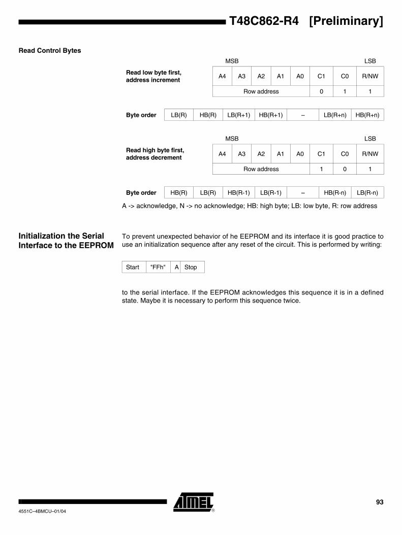
93
T48C862-R4 [Preliminary]
4551C–4BMCU–01/04
Read Control Bytes
A -> acknowledge, N -> no acknowledge; HB: high byte; LB: low byte, R: row address
Initialization the Serial Interface to the EEPROM
To prevent unexpected behavior of he EEPROM and its interface it is good practice touse an initialization sequence after any reset of the circuit. This is performed by writing:
to the serial interface. If the EEPROM acknowledges this sequence it is in a definedstate. Maybe it is necessary to perform this sequence twice.
MSB LSB
Read low byte first, address increment
A4 A3 A2 A1 A0 C1 C0 R/NW
Row address 0 1 1
Byte order LB(R) HB(R) LB(R+1) HB(R+1) – LB(R+n) HB(R+n)
MSB LSB
Read high byte first, address decrement A4 A3 A2 A1 A0 C1 C0 R/NW
Row address 1 0 1
Byte order HB(R) LB(R) HB(R-1) LB(R-1) – HB(R-n) LB(R-n)
Start "FFh" A Stop

94 T48C862-R4 [Preliminary] 4551C–4BMCU–01/04
Absolute Maximum Ratings: Microcontroller BlockStresses beyond those listed under “Absolute Maximum Ratings” may cause permanent damage to the device. This is a stress rating only and functional operation of the device at these or any other conditions beyond those indicated in the operational sections of this specification is not implied. Exposure to absolute maximum rating conditions for extended periods may affect device reliability.All inputs and outputs are protected against high electrostatic voltages or electric fields. However, precautions to minimize the build-up of electrostatic charges during handling are recommended. Reliability of operation is enhanced if unused inputs are connected to an appropriate logic voltage level (e.g., VDD).Voltages are given relative to VSS
Parameters Symbol Value Unit
Supply voltage VDD -0.3 to + 6.5 V
Input voltage (on any pin) VIN VSS -0.3 ≤ VIN ≤ VDD +0.3 V
Output short circuit duration tshort Indefinite s
Operating temperature range Tamb -40 to +125 ° C
Storage temperature range Tstg -40 to +150 ° C
Soldering temperature (t ≤ 10 s) Tsld 260 ° C
Thermal ResistanceParameter Symbol Value Unit
Thermal resistance RthJA 135 K/W
DC Operating CharacteristicsVSS = 0 V, Tamb = -40° C to +125° C unless otherwise specified.
Parameters Test Conditions Symbol Min. Typ. Max. Unit
Power Supply
Operating voltage at VDD VDD VPOR 4.0 V
Active currentCPU active
fSYSCL = 1 MHzVDD = 1.8 VVDD = 3.0 V
IDD 0.30.4 0.4
mAmA
Power down current (CPU sleep,RC oscillator active, 4-MHz quartz oscillator active)
fSYSCL = 1 MHzVDD = 1.8 VVDD = 3.0 V
IPD 4070 150
µAµA
Sleep current(CPU sleep,32-kHz quartz oscillator active4-MHz quartz oscillator inactive)
VDD = 1.8 VVDD = 3.0 VVDD = 3.0 V at 85° C
ISleep 0.40.6
4.31.5
µAµAµA
Sleep current(CPU sleep,32-kHz quartz oscillator inactive4-MHz quartz oscillator inactive)
VDD = 3.0 V VDD = 3.0 V at 85° C
ISleep0.3 3.5
1.0µAµA
Pin capacitance Any pin to VSS CL 7 10 pF
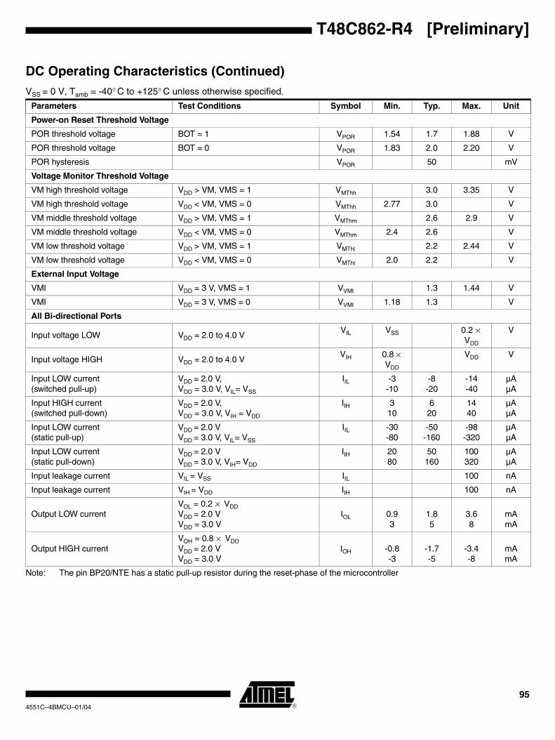
95
T48C862-R4 [Preliminary]
4551C–4BMCU–01/04
Note: The pin BP20/NTE has a static pull-up resistor during the reset-phase of the microcontroller
Power-on Reset Threshold Voltage
POR threshold voltage BOT = 1 VPOR 1.54 1.7 1.88 V
POR threshold voltage BOT = 0 VPOR 1.83 2.0 2.20 V
POR hysteresis VPOR 50 mV
Voltage Monitor Threshold Voltage
VM high threshold voltage VDD > VM, VMS = 1 VMThh 3.0 3.35 V
VM high threshold voltage VDD < VM, VMS = 0 VMThh 2.77 3.0 V
VM middle threshold voltage VDD > VM, VMS = 1 VMThm 2.6 2.9 V
VM middle threshold voltage VDD < VM, VMS = 0 VMThm 2.4 2.6 V
VM low threshold voltage VDD > VM, VMS = 1 VMThl 2.2 2.44 V
VM low threshold voltage VDD < VM, VMS = 0 VMThl 2.0 2.2 V
External Input Voltage
VMI VDD = 3 V, VMS = 1 VVMI 1.3 1.44 V
VMI VDD = 3 V, VMS = 0 VVMI 1.18 1.3 V
All Bi-directional Ports
Input voltage LOW VDD = 2.0 to 4.0 VVIL VSS 0.2 ×
VDD
V
Input voltage HIGH VDD = 2.0 to 4.0 VVIH 0.8 ×
VDD
VDD V
Input LOW current(switched pull-up)
VDD = 2.0 V,VDD = 3.0 V, VIL= VSS
IIL -3-10
-8-20
-14-40
µAµA
Input HIGH current(switched pull-down)
VDD = 2.0 V,VDD = 3.0 V, VIH = VDD
IIH 310
620
1440
µAµA
Input LOW current(static pull-up)
VDD = 2.0 VVDD = 3.0 V, VIL= VSS
IIL -30-80
-50-160
-98-320
µAµA
Input LOW current(static pull-down)
VDD = 2.0 VVDD = 3.0 V, VIH= VDD
IIH 2080
50160
100320
µAµA
Input leakage current VIL = VSS IIL 100 nA
Input leakage current VIH = VDD IIH 100 nA
Output LOW currentVOL = 0.2 × VDDVDD = 2.0 VVDD = 3.0 V
IOL 0.93
1.85
3.68
mAmA
Output HIGH currentVOH = 0.8 × VDDVDD = 2.0 VVDD = 3.0 V
IOH -0.8-3
-1.7-5
-3.4-8
mAmA
DC Operating Characteristics (Continued)VSS = 0 V, Tamb = -40° C to +125° C unless otherwise specified.
Parameters Test Conditions Symbol Min. Typ. Max. Unit
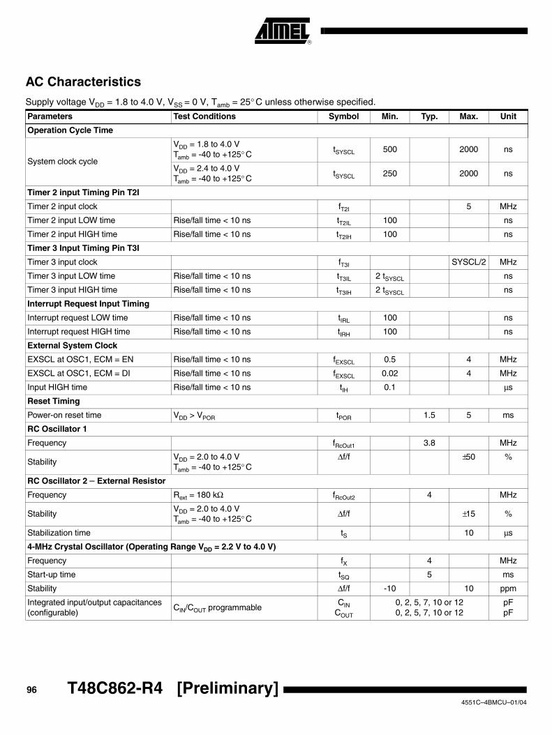
96 T48C862-R4 [Preliminary] 4551C–4BMCU–01/04
AC CharacteristicsSupply voltage VDD = 1.8 to 4.0 V, VSS = 0 V, Tamb = 25° C unless otherwise specified.
Parameters Test Conditions Symbol Min. Typ. Max. Unit
Operation Cycle Time
System clock cycle
VDD = 1.8 to 4.0 VTamb = -40 to +125° C
tSYSCL 500 2000 ns
VDD = 2.4 to 4.0 VTamb = -40 to +125° C
tSYSCL 250 2000 ns
Timer 2 input Timing Pin T2I
Timer 2 input clock fT2I 5 MHz
Timer 2 input LOW time Rise/fall time < 10 ns tT2IL 100 ns
Timer 2 input HIGH time Rise/fall time < 10 ns tT2IH 100 ns
Timer 3 Input Timing Pin T3I
Timer 3 input clock fT3I SYSCL/2 MHz
Timer 3 input LOW time Rise/fall time < 10 ns tT3IL 2 tSYSCL ns
Timer 3 input HIGH time Rise/fall time < 10 ns tT3IH 2 tSYSCL ns
Interrupt Request Input Timing
Interrupt request LOW time Rise/fall time < 10 ns tIRL 100 ns
Interrupt request HIGH time Rise/fall time < 10 ns tIRH 100 ns
External System Clock
EXSCL at OSC1, ECM = EN Rise/fall time < 10 ns fEXSCL 0.5 4 MHz
EXSCL at OSC1, ECM = DI Rise/fall time < 10 ns fEXSCL 0.02 4 MHz
Input HIGH time Rise/fall time < 10 ns tIH 0.1 µs
Reset Timing
Power-on reset time VDD > VPOR tPOR 1.5 5 ms
RC Oscillator 1
Frequency fRcOut1 3.8 MHz
StabilityVDD = 2.0 to 4.0 VTamb = -40 to +125° C
∆f/f ±50 %
RC Oscillator 2 – External Resistor
Frequency Rext = 180 kΩ fRcOut2 4 MHz
StabilityVDD = 2.0 to 4.0 VTamb = -40 to +125° C
∆f/f ±15 %
Stabilization time tS 10 µs
4-MHz Crystal Oscillator (Operating Range VDD = 2.2 V to 4.0 V)
Frequency fX 4 MHz
Start-up time tSQ 5 ms
Stability ∆f/f -10 10 ppm
Integrated input/output capacitances (configurable)
CIN/COUT programmable CIN
COUT
0, 2, 5, 7, 10 or 120, 2, 5, 7, 10 or 12
pFpF
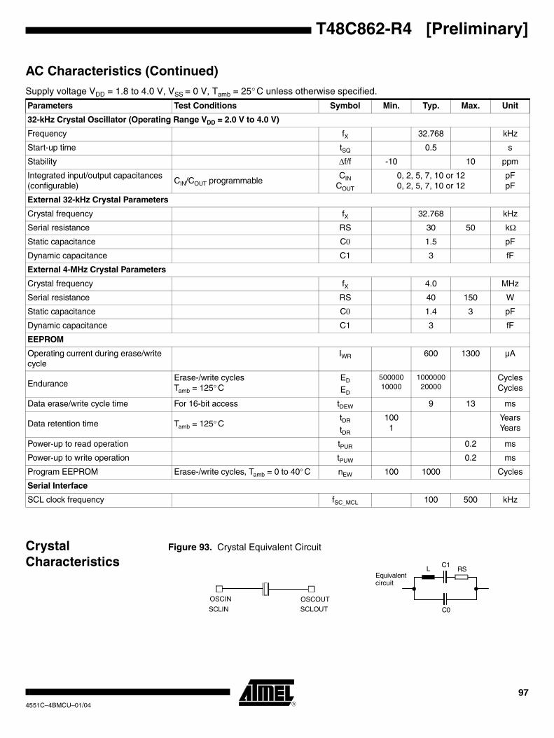
97
T48C862-R4 [Preliminary]
4551C–4BMCU–01/04
Crystal Characteristics
Figure 93. Crystal Equivalent Circuit
32-kHz Crystal Oscillator (Operating Range VDD = 2.0 V to 4.0 V)
Frequency fX 32.768 kHz
Start-up time tSQ 0.5 s
Stability ∆f/f -10 10 ppm
Integrated input/output capacitances (configurable)
CIN/COUT programmable CIN
COUT
0, 2, 5, 7, 10 or 120, 2, 5, 7, 10 or 12
pFpF
External 32-kHz Crystal Parameters
Crystal frequency fX 32.768 kHz
Serial resistance RS 30 50 kΩ
Static capacitance C0 1.5 pF
Dynamic capacitance C1 3 fF
External 4-MHz Crystal Parameters
Crystal frequency fX 4.0 MHz
Serial resistance RS 40 150 W
Static capacitance C0 1.4 3 pF
Dynamic capacitance C1 3 fF
EEPROM
Operating current during erase/write cycle
IWR 600 1300 µA
EnduranceErase-/write cyclesTamb = 125° C
ED
ED
50000010000
100000020000
CyclesCycles
Data erase/write cycle time For 16-bit access tDEW 9 13 ms
Data retention time Tamb = 125° CtDR
tDR
1001
YearsYears
Power-up to read operation tPUR 0.2 ms
Power-up to write operation tPUW 0.2 ms
Program EEPROM Erase-/write cycles, Tamb = 0 to 40° C nEW 100 1000 Cycles
Serial Interface
SCL clock frequency fSC_MCL 100 500 kHz
AC Characteristics (Continued)Supply voltage VDD = 1.8 to 4.0 V, VSS = 0 V, Tamb = 25° C unless otherwise specified.
Parameters Test Conditions Symbol Min. Typ. Max. Unit
L C1RS
C0
OSCIN OSCOUT
Equivalentcircuit
SCLIN SCLOUT

98 T48C862-R4 [Preliminary] 4551C–4BMCU–01/04
Emulation The basic function of emulation is to test and evaluate the customer's program andhardware in real time. This therefore enables the analysis of any timing, hardware orsoftware problem. For emulation purposes, all MARC4 controllers include a specialemulation mode. In this mode, the internal CPU core is inactive and the I/O buses areavailable via Port 0 and Port 1 to allow an external access to the on-chip peripherals.The MARC4 emulator uses this mode to control the peripherals of any MARC4 control-ler (target chip) and emulates the lost ports for the application.
The MARC4 emulator can stop and restart a program at specified points during execu-tion, making it possible for the applications engineer to view the memory contents andthose of various registers during program execution. The designer also gains the abilityto analyze the executed instruction sequences and all the I/O activities.
Figure 94. MARC4 Emulation
MARC4 target chip
CORE(inactive)
Por
t 1P
ort 0
Application-specific hardware
Peripherals
MARC4 emulator
Programmemory
Tracememory
Control logic
Personal computer
CORE
MARC4emulation-CPU
I/O control
I/O bus
Port 0 Port 1SYSCL/
TCL,TE, NRST
Emulation control
Emulator target board

99
T48C862-R4 [Preliminary]
4551C–4BMCU–01/04
Please attach this page to the approval form.
Date: ____________ Signature: _________________________Company: _________________________
Option Settings for OrderingPlease select the option settings from the list below and insert ROM CRC.
Output Input Output Input
Port 1 Port 5
BP10 [ ] CMOS [ ] Switched pull-up BP50 [ ] CMOS [ ] Switched pull-up
[ ] Open drain [N] [ ] Switched pull-down [ ] Open drain [N] [ ] Switched pull-down
[ ] Open drain [P] [ ] Static pull-up [ ] Open drain [P] [ ] Static pull-up
[ ] Static pull-down [ ] Static pull-down
BP13 [ ] CMOS [ ] Switched pull-up BP51 [ ] CMOS [ ] Switched pull-up
[ ] Open drain [N] [ ] Switched pull-down [ ] Open drain [N] [ ] Switched pull-down
[ ] Open drain [P] [ ] Static pull-up [ ] Open drain [P] [ ] Static pull-up
[ ] Static pull-down [ ] Static pull-down
Port 2 BP52 [ ] CMOS [ ] Switched pull-up
BP20 [ ] CMOS [ ] Switched pull-up [ ] Open drain [N] [ ] Switched pull-down
[ ] Open drain [N] [ ] Switched pull-down [ ] Open drain [P] [ ] Static pull-up
[ ] Open drain [P] [ ] Static pull-up [ ] Static pull-down
BP53 [ ] CMOS [ ] Switched pull-up
BP21 [ ] CMOS [ ] Switched pull-up [ ] Open drain [N] [ ] Switched pull-down
[ ] Open drain [N] [ ] Switched pull-down [ ] Open drain [P] [ ] Static pull-up
[ ] Open drain [P] [ ] Static pull-up [ ] Static pull-down
[ ] Static pull-down Port 6
BP22 [ ] CMOS [ ] Switched pull-up BP60 [ ] CMOS [ ] Switched pull-up
[ ] Open drain [N] [ ] Switched pull-down [ ] Open drain [N] [ ] Switched pull-down
[ ] Open drain [P] [ ] Static pull-up [ ] Open drain [P] [ ] Static pull-up
[ ] Static pull-down [ ] Static pull-down
BP23 [ ] CMOS [ ] Switched pull-up BP63 [ ] CMOS [ ] Switched pull-up
[ ] Open drain [N] [ ] Switched pull-down [ ] Open drain [N] [ ] Switched pull-down
[ ] Open drain [P] [ ] Static pull-up [ ] Open drain [P] [ ] Static pull-up
[ ] Static pull-down [ ] Static pull-down
Port 4
BP40 [ ] CMOS [ ] Switched pull-up OSC1
[ ] Open drain [N] [ ] Switched pull-down [ ] No integrated capacitance
[ ] Open drain [P] [ ] Static pull-up [ ] Internal capacitance (0 to 20 pF) [ _____pF]
[ ] Static pull-down OSC2
BP41 [ ] CMOS [ ] Switched pull-up [ ] No integrated capacitance
[ ] Open drain [N] [ ] Switched pull-down [ ] Internal capacitance (0 to 20 pF) [ _____pF]
[ ] Open drain [P] [ ] Static pull-up
[ ] Static pull-down Clock Used
BP42 [ ] CMOS [ ] Switched pull-up [ ] External resistor
[ ] Open drain [N] [ ] Switched pull-down [ ] External clock
[ ] Open drain [P] [ ] Static pull-up [ ] 32-kHz crystal
[ ] Static pull-down [ ] 4-MHz crystal
BP43 [ ] CMOS [ ] Switched pull-up
[ ] Open drain [N] [ ] Switched pull-down ECM (External Clock Monitor)
[ ] Open drain [P] [ ] Static pull-up [ ] Enable
[ ] Static pull-down [ ] Disable
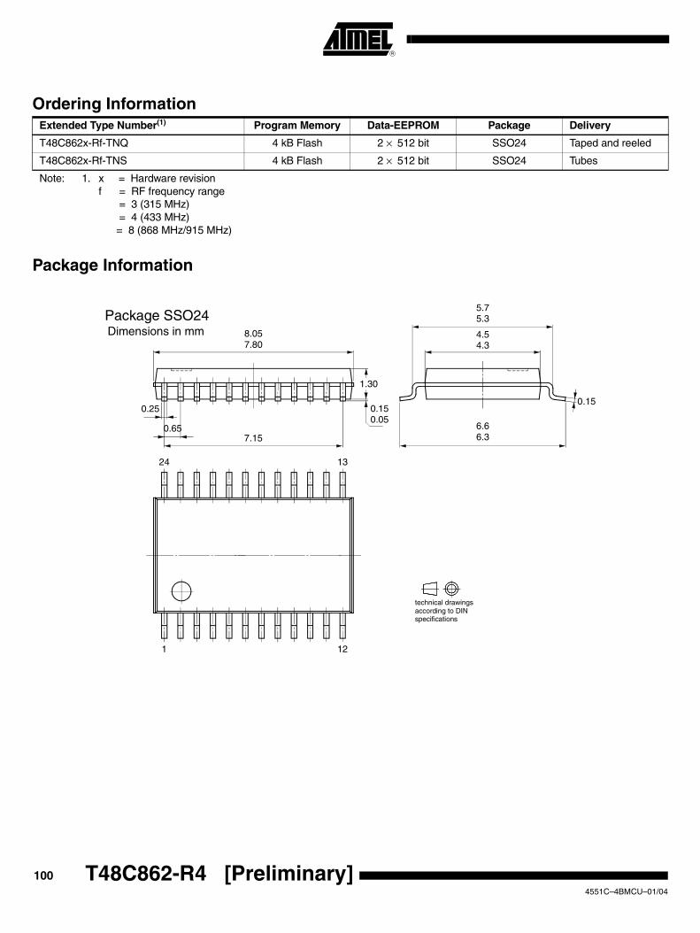
100 T48C862-R4 [Preliminary] 4551C–4BMCU–01/04
Package Information
Ordering InformationExtended Type Number(1) Program Memory Data-EEPROM Package Delivery
T48C862x-Rf-TNQ 4 kB Flash 2 × 512 bit SSO24 Taped and reeled
T48C862x-Rf-TNS 4 kB Flash 2 × 512 bit SSO24 Tubes
Note: 1. x = Hardware revisionf = RF frequency range
= 3 (315 MHz)= 4 (433 MHz)= 8 (868 MHz/915 MHz)
technical drawingsaccording to DINspecifications
Package SSO24Dimensions in mm 8.05
7.80
0.150.05
0.25
0.657.15
1.30
5.75.3
4.54.3
6.66.3
0.15
24 13
1 12

101
T48C862-R4 [Preliminary]
4551C–4BMCU–01/04
Table of Contents Features................................................................................................. 1
Description ............................................................................................ 1
Pin Configuration.................................................................................. 2
Pin Description: RF Part ...................................................................... 2
Pin Description: Microcontroller Part ................................................. 3
UHF ASK/FSK Transmitter Block ........................................................ 4
Features................................................................................................. 4
Description ............................................................................................ 4
General Description.............................................................................. 6
Functional Description......................................................................... 6ASK Transmission ................................................................................................ 6FSK Transmission ................................................................................................ 6CLK Output ........................................................................................................... 7
Clock Pulse Take Over ...................................................................................7Output Matching and Power Setting ...............................................................7
Application Circuit ................................................................................................. 8
Absolute Maximum Ratings: RF Part................................................ 11
Thermal Resistance............................................................................ 11
Electrical Characteristics................................................................... 11
Microcontroller Block......................................................................... 13
Features............................................................................................... 13
Description .......................................................................................... 13
Introduction......................................................................................... 13Differences between T48C862-R4 and ATAR862 Microcontrollers ................... 13
Program Memory ..........................................................................................13Configuration Memory ...................................................................................13Data Memory ................................................................................................13Reset Function ..............................................................................................14
MARC4 Architecture General Description........................................ 14
102 T48C862-R4 [Preliminary] 4551C–4BMCU–01/04
Components of MARC4 Core ............................................................ 14Program Memory ................................................................................................ 14RAM.................................................................................................................... 15
Expression Stack ..........................................................................................15Return Stack .................................................................................................15
Registers............................................................................................................. 16Program Counter (PC) ..................................................................................16RAM Address Registers ................................................................................17Expression Stack Pointer (SP) ......................................................................17Return Stack Pointer (RP) ............................................................................17RAM Address Registers (X and Y) ...............................................................17Top of Stack (TOS) .......................................................................................17Condition Code Register (CCR) ....................................................................17Carry/Borrow (C) ...........................................................................................17Branch (B) .....................................................................................................17Interrupt Enable (I) ........................................................................................17
ALU..................................................................................................................... 18I/O Bus................................................................................................................ 18Instruction Set..................................................................................................... 18Interrupt Structure............................................................................................... 18
Interrupt Processing ......................................................................................19Interrupt Latency ...........................................................................................19
Software Interrupts ............................................................................................. 20Hardware Interrupts ............................................................................................ 20
Master Reset ....................................................................................... 21Power-on Reset and Brown-out Detection ......................................................... 21
Watchdog Reset ...........................................................................................22External Clock Supervisor .............................................................................22
Voltage Monitor................................................................................... 22Voltage Monitor Control/Status Register .......................................................23
Clock Generation ................................................................................ 24Clock Module ...................................................................................................... 24Oscillator Circuits and External Clock Input Stage ............................................. 25
RC-oscillator 1 Fully Integrated .....................................................................25External Input Clock ......................................................................................26RC-oscillator 2 with External Trimming Resistor ...........................................264-MHz Oscillator ...........................................................................................2732-kHz Oscillator ...........................................................................................27
Clock Management............................................................................................. 28Clock Management Register (CM) ................................................................28System Configuration Register (SC) .............................................................29
Power-down Modes ............................................................................ 29
103
T48C862-R4 [Preliminary]
4551C–4BMCU–01/04
Peripheral Modules............................................................................. 30Addressing Peripherals....................................................................................... 30
Bi-directional Ports............................................................................. 33Bi-directional Port 1 ............................................................................................ 33Bi-directional Port 2 ............................................................................................ 34
Port 2 Data Register (P2DAT) ......................................................................35Port 2 Control Register (P2CR) ....................................................................35
Bi-directional Port 5 ............................................................................................ 35Port 5 Data Register (P5DAT) ......................................................................36Port 5 Control Register (P5CR) Byte Write ...................................................36
Bi-directional Port 4 ............................................................................................ 37Port 4 Data Register (P4DAT) ......................................................................38Port 4 Control Register (P4CR) Byte Write ...................................................38
Bi-directional Port 6 ............................................................................................ 38Port 6 Data Register (P6DAT) ......................................................................39Port 6 Control Register (P6CR) ....................................................................39
Universal Timer/Counter/ Communication Module (UTCM) ............................... 39Timer 1................................................................................................................ 40
Timer 1 Control Register 1 (T1C1) ................................................................42Timer 1 Control Register 2 (T1C2) ................................................................43Watchdog Control Register (WDC) ...............................................................43
Timer 2................................................................................................................ 44Timer 2 Modes.................................................................................................... 45
Mode 1: 12-bit Compare Counter .................................................................45Mode 2: 8-bit Compare Counter with 4-bit Programmable Prescaler ...........45Mode 3/4: 8-bit Compare Counter and 4-bit Programmable Prescaler .........46
Timer 2 Output Modes ........................................................................................ 46Timer 2 Output Signals ....................................................................................... 47
Timer 2 Output Mode 1 .................................................................................47Timer 2 Output Mode 2 .................................................................................48Timer 2 Output Mode 3 .................................................................................48Timer 2 Output Mode 4 .................................................................................49Timer 2 Output Mode 5 .................................................................................49Timer 2 Output Mode 7 .................................................................................49
Timer 2 Registers ............................................................................................... 50Timer 2 Control Register (T2C) .....................................................................50Timer 2 Mode Register 1 (T2M1) ..................................................................50Duty Cycle Generator ...................................................................................51Timer 2 Mode Register 2 (T2M2) ..................................................................52Timer 2 Compare and Compare Mode Registers .........................................52Timer 2 Compare Mode Register (T2CM) ....................................................53Timer 2 COmpare Register 1 (T2CO1) .........................................................53Timer 2 COmpare Register 2 (T2CO2) Byte Write .......................................53
Timer 3 ................................................................................................. 54

104 T48C862-R4 [Preliminary] 4551C–4BMCU–01/04
Features ........................................................................................................54Timer/Counter Modes ......................................................................................... 55
Timer 3 – Mode 1: Timer/Counter .................................................................56Timer 3 – Mode 2: Timer/Counter, External Trigger Restart and External
Capture (with T3I Input) ...............................................57Timer 3 – Mode 3: Timer/Counter, Internal Trigger Restart and Internal
Capture (with TOG2) ...................................................58Timer 3 – Mode 4: Timer/Counter .................................................................58Timer 3 – Mode 5: Timer/Counter, External Trigger Restart and External
Capture (with T3I Input) ...............................................58Timer 3 Modulator/Demodulator Modes ............................................................. 58
Timer 3 – Mode 6: Carrier Frequency Burst Modulation Controlled by Timer 2 Output Toggle Flip-Flop (M2) ........................58
Timer 3 – Mode 7: Carrier Frequency Burst Modulation Controlled by SSI Internal Output (SO) .............................................59
Timer 3 – Mode 8: FSK Modulation with Shift Register Data (SO) ...............59Timer 3 – Mode 9: Pulse-width Modulation with the Shift Register ...............59Timer 3 – Mode 10: Manchester Demodulation/Pulse-width Demodulation .60Timer 3 – Mode 11: Biphase Demodulation ..................................................60Timer 3 – Mode 12: Timer/Counter with External Capture Mode (T3I) .........61
Timer 3 Modulator for Carrier Frequency Burst Modulation ............................... 61Timer 3 Demodulator for Biphase, Manchester and Pulse-width-modulated
Signals................................................................................................. 61Timer 3 Registers ............................................................................................... 62
Timer 3 Mode Register (T3M) .......................................................................62Timer 3 Control Register 1 (T3C) Write ........................................................63Timer 3 Status Register 1 (T3ST) Read .......................................................63Timer 3 Clock Select Register (T3CS) ..........................................................64Timer 3 Compare- and Compare-mode Register .........................................64Timer 3 Compare-Mode Register 1 (T3CM1) ...............................................65Timer 3 Compare Mode Register 2 (T3CM2) ...............................................65Timer 3 COmpare Register 1 (T3CO1) Byte Write .......................................66Timer 3 COmpare Register 2 (T3CO2) Byte Write .......................................66
Timer 3 Capture Register ................................................................................... 66Timer 3 CaPture Register (T3CP) Byte Read ...............................................66
Synchronous Serial Interface (SSI) .................................................................... 67SSI Features: ................................................................................................67SSI Peripheral Configuration ........................................................................67General SSI Operation ..................................................................................688-bit Synchronous Mode ...............................................................................699-bit Shift Mode (MCL) ..................................................................................718-bit Pseudo MCL Mode ...............................................................................72MCL Bus Protocol .........................................................................................72SSI Interrupt ..................................................................................................74Modulation and Demodulation ......................................................................74
Serial Interface Registers ................................................................................... 75Serial Interface Control Register 1 (SIC1) ....................................................75
105
T48C862-R4 [Preliminary]
4551C–4BMCU–01/04
Serial Interface Control Register 2 (SIC2) ....................................................76Serial Interface Status and Control Register (SISC) .....................................77Serial Transmit Buffer (STB) – Byte Write ....................................................77Serial Receive Buffer (SRB) – Byte Read .....................................................78
Combination Modes ........................................................................... 78Combination Mode Timer 2 and SSI................................................................... 78
Combination Mode 1: Burst Modulation ........................................................79Combination Mode 2: Biphase Modulation 1 ................................................79Combination Mode 3: Manchester Modulation 1 ..........................................80Combination Mode 4: Manchester Modulation 2 ..........................................80Combination Mode 5: Biphase Modulation 2 ................................................81
Combination Mode Timer 3 and SSI................................................................... 82Combination Mode 6: FSK Modulation .........................................................82Combination Mode 7: Pulse-width Modulation (PWM) .................................83Combination Mode 8: Manchester Demodulation/
Pulse-width Demodulation ......................................83Combination Mode 9: Biphase Demodulation ...............................................84
Combination Mode Timer 2 and Timer 3 ............................................................ 85Combination Mode 10: Frequency Measurement or Event Counter with
Time Gate .............................................................85Combination Mode 11: Burst Modulation 1 ...................................................86
Combination Mode Timer 2, Timer 3 and SSI .................................................... 87Combination Mode 12: Burst Modulation 2 ...................................................88Combination Mode 13: FSK Modulation .......................................................88
Data EEPROM.................................................................................................... 89Serial Interface.................................................................................................... 90
Serial Protocol ...............................................................................................90Control Byte Format ......................................................................................91
EEPROM ............................................................................................................ 91EEPROM – Operating Modes .......................................................................91Write Operations ...........................................................................................91Acknowledge Polling .....................................................................................91Write One Data Byte .....................................................................................91Write Two Data Bytes ...................................................................................91Write Control Byte Only ................................................................................91Write Control Bytes .......................................................................................92Read Operations ...........................................................................................92Read One Data Byte .....................................................................................92Read Two Data Bytes ...................................................................................92Read n Data Bytes ........................................................................................92Read Control Bytes .......................................................................................93
Initialization the Serial Interface to the EEPROM ............................................... 93
Absolute Maximum Ratings: Microcontroller Block ....................... 94
106 T48C862-R4 [Preliminary] 4551C–4BMCU–01/04
Thermal Resistance............................................................................ 94
DC Operating Characteristics............................................................ 94
AC Characteristics.............................................................................. 96
Crystal Characteristics....................................................................... 97Emulation............................................................................................................ 98
Option Settings for Ordering ............................................................. 99
Ordering Information........................................................................ 100
Package Information ........................................................................ 100
Table of Contents ............................................................................. 101
Printed on recycled paper.
Disclaimer: Atmel Corporation makes no warranty for the use of its products, other than those expressly contained in the Company’s standardwarranty which is detailed in Atmel’s Terms and Conditions located on the Company’s web site. The Company assumes no responsibility for anyerrors which may appear in this document, reserves the right to change devices or specifications detailed herein at any time without notice, anddoes not make any commitment to update the information contained herein. No licenses to patents or other intellectual property of Atmel aregranted by the Company in connection with the sale of Atmel products, expressly or by implication. Atmel’s products are not authorized for useas critical components in life support devices or systems.
Atmel Corporation Atmel Operations
2325 Orchard ParkwaySan Jose, CA 95131, USATel: 1(408) 441-0311Fax: 1(408) 487-2600
Regional Headquarters
EuropeAtmel SarlRoute des Arsenaux 41Case Postale 80CH-1705 FribourgSwitzerlandTel: (41) 26-426-5555Fax: (41) 26-426-5500
AsiaRoom 1219Chinachem Golden Plaza77 Mody Road TsimshatsuiEast KowloonHong KongTel: (852) 2721-9778Fax: (852) 2722-1369
Japan9F, Tonetsu Shinkawa Bldg.1-24-8 ShinkawaChuo-ku, Tokyo 104-0033JapanTel: (81) 3-3523-3551Fax: (81) 3-3523-7581
Memory2325 Orchard ParkwaySan Jose, CA 95131, USATel: 1(408) 441-0311Fax: 1(408) 436-4314
Microcontrollers2325 Orchard ParkwaySan Jose, CA 95131, USATel: 1(408) 441-0311Fax: 1(408) 436-4314
La ChantrerieBP 7060244306 Nantes Cedex 3, FranceTel: (33) 2-40-18-18-18Fax: (33) 2-40-18-19-60
ASIC/ASSP/Smart CardsZone Industrielle13106 Rousset Cedex, FranceTel: (33) 4-42-53-60-00Fax: (33) 4-42-53-60-01
1150 East Cheyenne Mtn. Blvd.Colorado Springs, CO 80906, USATel: 1(719) 576-3300Fax: 1(719) 540-1759
Scottish Enterprise Technology ParkMaxwell BuildingEast Kilbride G75 0QR, Scotland Tel: (44) 1355-803-000Fax: (44) 1355-242-743
RF/AutomotiveTheresienstrasse 2Postfach 353574025 Heilbronn, GermanyTel: (49) 71-31-67-0Fax: (49) 71-31-67-2340
1150 East Cheyenne Mtn. Blvd.Colorado Springs, CO 80906, USATel: 1(719) 576-3300Fax: 1(719) 540-1759
Biometrics/Imaging/Hi-Rel MPU/High Speed Converters/RF Datacom
Avenue de RochepleineBP 12338521 Saint-Egreve Cedex, FranceTel: (33) 4-76-58-30-00Fax: (33) 4-76-58-34-80
Literature Requestswww.atmel.com/literature
4551C–4BMCU–01/04
© Atmel Corporation 2004. All rights reserved.
Atmel® and combinations thereof are the registered trademarks of Atmel Corporation or its subsidiaries.
Other terms and product names may be the trademarks of others.