Embed Size (px)
Citation preview

Solar Energy Materials & Solar Cells 74 (2002) 457–467
Microcrystalline silicon and the impact onmicromorph tandem solar cells
J. Meier*, S. Dubail, S. Golay, U. Kroll, S. Fa.y,E. Vallat-Sauvain, L. Feitknecht, J. Dubail1, A. Shah
Institut de Microtechnique (IMT), A.-L. Breguet 2, Universit!e de Neuch #atel, CH-2000 Neuch #atel,
Switzerland
Abstract
Intrinsic microcrystalline silicon opens up new ways for silicon thin-film multi-junction solar
cells, the most promising being the ‘‘micromorph’’ tandem concept. The microstructure of
entirely microcrystalline p–i–n solar cells is investigated by transmission electron microscopy.
By applying low pressure chemical vapor deposition ZnO as front TCO in p–i–n configurated
micromorph tandems, a remarkable reduction of the microcrystalline bottom cell thickness is
achieved. Micromorph tandem cells with high open circuit voltages of 1.413V could be
accomplished. A stabilized efficiency of around 11% is estimated for micromorph tandems
consisting of 2 mm thick bottom cells. Applying the monolithic series connection, a
micromorph module (23.3 cm2) of 9.1% stabilized efficiency could be obtained. r 2002
Elsevier Science B.V. All rights reserved.
Keywords: Hydrogenated microcrystalline silicon; Thin-film silicon; VHF-GD; LP-CVD ZnO; Light-
trapping
1. Introduction
In 1994, our group at Institute of Microtechnology (IMT) Neuch#atel succeeded inthe preparation of a fully microcrystalline (mc-Si:H) silicon p–i–n single-junctionsolar cell with new striking advantages compared to amorphous silicon (a-Si:H) [1]:This new photovoltaic absorber material shows no light-induced degradation unlikea-Si:H, and has a lower band gap than a-Si:H, i.e. a higher current potential for solarcells. In the same year, IMT also presented the ‘‘micromorph’’ concept consisting of
*Corresponding author. Fax: +41-32-718-3201.
E-mail address: [email protected] (J. Meier).1At present with API Portescap, rue Jardini"ere, CH-2301 La Chaux-de-Fonds.
0927-0248/02/$ - see front matter r 2002 Elsevier Science B.V. All rights reserved.
PII: S 0 9 2 7 - 0 2 4 8 ( 0 2 ) 0 0 1 1 1 - 3
an amorphous silicon top cell and a microcrystalline silicon bottom cell [2]. Thisoriginal work was pioneered from the beginning in the ‘‘superstrate configuration’’,e.g. p–i–n/p–i–n tandem cells were deposited on a glass substrate coated withtransparent conductive oxide (TCO). With this new concept, stabilized cellefficiencies in the range of 11–12% have been achieved [3–7]. This type of thin-film solar cell, based on silicon alone, is today considered to be one of the mostpromising cell concepts with respect to cost reduction with simultaneous efficiencyenhancement, availability of raw materials and technological feasibility of up-scalingto large-area modules. For the deposition of microcrystalline silicon, the samedeposition equipment can, in principle, be used as in the case of amorphous silicon.The latter is at present the only thin-film solar cell that has established itself for MW-scale manufacturing. Recently, Kaneka Corp. changed their strategy by adoptingIMT’s original concept of a superstrate micromorph tandem configuration depositedon glass (called ‘‘hybrid’’ solar cells by them) and visibly substantially reducing theirdeposition temperature. Thereby, they were able to fabricate large-area PV‘‘micromorph’’ or ‘‘hybrid’’ modules of 0.4m2 size [8], that have since beenintroduced into the European market. These modules show initial efficiencies closeto 10%, which are well above those that are currently obtained for commerciallymass-produced amorphous silicon-based solar modules. Thus, one can say thatmicromorph tandems open up a new efficiency segment range for thin-film solarcells; indeed, they have the potential for overlapping with the region of wafer-basedsolar cells, especially when taking the better temperature coefficient of micromorphtandems into account and considering solar module performance under real outdoorworking conditions [4,8].
As crystalline silicon is a material with an indirect band gap, the opticalabsorption coefficient for photon energies just over the band gap is relatively low.This means that in a micromorph tandem, the microcrystalline bottom cell will haveto be thicker than the amorphous top cell in order to obtain current matchingconditions. The challenge of making micromorph cells economically viable is giventherefore not only by the question of obtaining higher efficiencies, but by thetechnological aspect of achieving high deposition rates and the further aspect ofoptimizing the light-trapping for the thin-film cell. A highly efficient light-trappingallows for the reduction of the thickness of the mc-Si:H bottom cell, and a highdeposition rate allows for a high throughput. Both are important factors for theeconomical manufacturing of micromorph tandems. The key question is to whatextent the mc-Si:H cell thickness can be reduced while still achieving optimalefficiency potential for micromorph modules.
2. Results and discussion
2.1. Microcrystalline silicon p–i–n cells
As microcrystalline silicon cells do not show any light-induced degradation effect,this material can be considered to be an interesting substitute for low-band gap
J. Meier et al. / Solar Energy Materials & Solar Cells 74 (2002) 457–467458
amorphous silicon–germanium alloys based on the use of germane (an expensivesource gas). For this reason, broad research has been started by different groups onmicrocrystalline silicon solar cells.
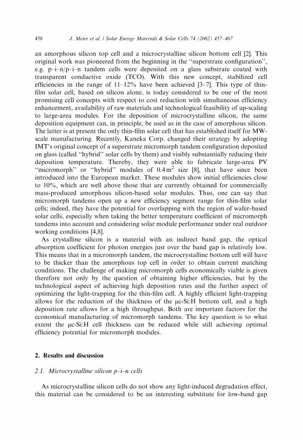
In the early phase of pioneering microcrystalline silicon as PV material, single-junction devices showed rather low open circuit voltages (Voc) of barely 400mV [1].In the meantime, remarkably high Voc-values of between 520 and 550mV could beobtained by different groups [5,9–12]. Fig. 1 gives the I–V characteristics for acorresponding mc-Si:H p–i–n cell fabricated at IMT.
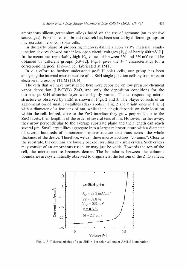
In our effort to further understand mc-Si:H solar cells, our group has beenanalyzing the internal microstructure of mc-Si:H single-junction cells by transmissionelectron microscopy (TEM) [13,14].
The cells that we have investigated here were deposited on low pressure chemicalvapor deposition (LP-CVD) ZnO, and only the deposition conditions for theintrinsic mc-Si:H absorber layer were slightly varied. The corresponding micro-structure as observed by TEM is shown in Figs. 2 and 3. The i-layer consists of anagglomeration of small crystallites (dark spots in Fig. 2 and bright ones in Fig. 3)with a diameter of a few tens of nm, while their length depends on their locationwithin the cell. Indeed, close to the ZnO interface they grow perpendicular to theZnO facets; their length is of the order of several tens of nm. However, further away,they grow perpendicular to the average substrate plane and their length can reachseveral mm. Small crystallites aggregate into a larger microstructure with a diameterof several hundreds of nanometers—microstructure that runs across the wholethickness of the device. Therefore, we call these microstructures ‘‘columns’’. Close tothe substrate, the columns are loosely packed, resulting in visible cracks. Such cracksmay consist of an amorphous tissue, or may just be voids. Towards the top of thecell, the microstructure becomes denser. The boundaries between the columnsboundaries are systematically observed to originate at the bottom of the ZnO valleys.
-25
-20
-15
-10
-5
0
0 0.5
Cur
rent
[mA
/cm
2]
Voltage [V]
µc-Si:H p-i-n
Jsc = 22.9 mA/cm2
FF = 69.8 %Voc = 531 mV
(d = 2.7 µm)
η η = 8.5 %
Fig. 1. I–V characteristics of a mc-Si:H p–i–n solar cell under AM1.5 illumination.
J. Meier et al. / Solar Energy Materials & Solar Cells 74 (2002) 457–467 459
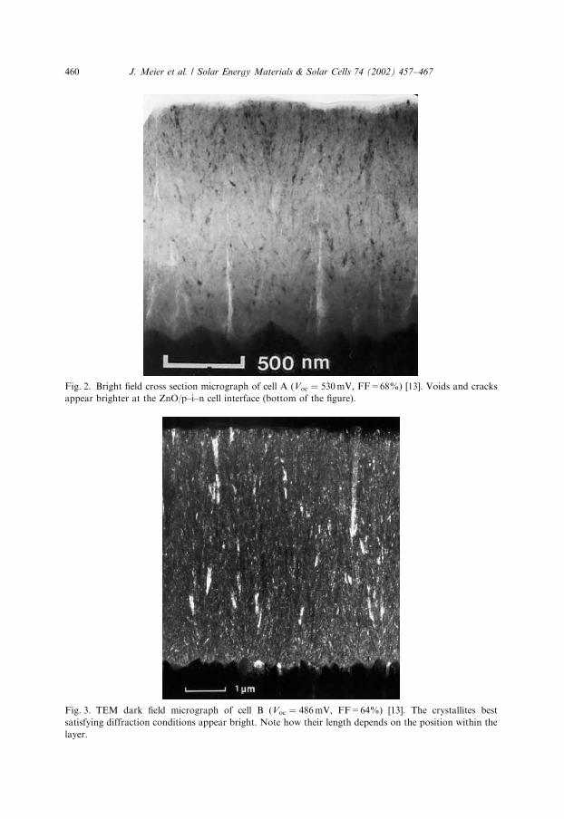
Fig. 2. Bright field cross section micrograph of cell A (Voc ¼ 530mV, FF=68%) [13]. Voids and cracks
appear brighter at the ZnO/p–i–n cell interface (bottom of the figure).
Fig. 3. TEM dark field micrograph of cell B (Voc ¼ 486mV, FF=64%) [13]. The crystallites best
satisfying diffraction conditions appear bright. Note how their length depends on the position within the
layer.
J. Meier et al. / Solar Energy Materials & Solar Cells 74 (2002) 457–467460
As the cells have quite different thicknesses, the electrical characteristics can becompared only with respect to their Voc- and FF-values. Surprisingly, the Voc- andFF-values are higher for the cell in Fig. 2 (than for the cell in Fig. 3), i.e. higher forthat cell that exhibits voids at the ZnO p–i interface, as these voids are considered tobe responsible for shunting the solar cell. In order to get more insight into therelationship between device characteristics and microstructure, more systematicTEM investigations have to be done [15].
2.2. Light-trapping
In thin-film silicon solar cells, light-trapping is a key issue for two reasons: (1) bothfor realizing the full efficiency potential, and (2) for reducing the absorber thicknessand, thus, the fabrication time. Light-trapping, therefore, contributes much toreduce the cost per Wpeak: To improve light-trapping, IMT has developed its own in-house TCO, namely zinc oxide prepared by LP-CVD [16]. The typical surfacemorphology of such a ZnO layer is shown in Fig. 4 by means of a SEM micrographand is compared with the best commercially available (but expensive) TCO, as can befound on SnO2-coated glass substrates from Asahi (type U). In the present paper,recent results w.r.t. its use in micromorph tandem solar cells will be extended.
The LP-CVD ZnO developed by IMT has already proven its effectiveness inachieving a considerable improvement of the performance for single-junctionamorphous silicon (a-Si:H) solar cells (see Fig. 5) as compared to SnO2 (type U) [17].Our amorphous silicon p–i–n solar cells on LP-CVD ZnO TCO have independently
Fig. 4. SEM micrographs of a SnO2 Asahi type U substrate (left) and of a typical as-grown LP-CVD ZnO
layer (right) used for p–i–n configurated solar cells.
J. Meier et al. / Solar Energy Materials & Solar Cells 74 (2002) 457–467 461
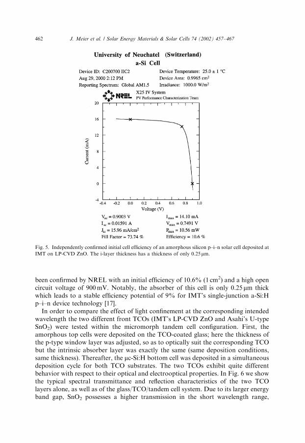
been confirmed by NREL with an initial efficiency of 10.6% (1 cm2) and a high opencircuit voltage of 900mV. Notably, the absorber of this cell is only 0.25 mm thickwhich leads to a stable efficiency potential of 9% for IMT’s single-junction a-Si:Hp–i–n device technology [17].
In order to compare the effect of light confinement at the corresponding intendedwavelength the two different front TCOs (IMT’s LP-CVD ZnO and Asahi’s U-typeSnO2) were tested within the micromorph tandem cell configuration. First, theamorphous top cells were deposited on the TCO-coated glass; here the thickness ofthe p-type window layer was adjusted, so as to optically suit the corresponding TCObut the intrinsic absorber layer was exactly the same (same deposition conditions,same thickness). Thereafter, the mc-Si:H bottom cell was deposited in a simultaneousdeposition cycle for both TCO substrates. The two TCOs exhibit quite differentbehavior with respect to their optical and electrooptical properties. In Fig. 6 we showthe typical spectral transmittance and reflection characteristics of the two TCOlayers alone, as well as of the glass/TCO/tandem cell system. Due to its larger energyband gap, SnO2 possesses a higher transmission in the short wavelength range,
Fig. 5. Independently confirmed initial cell efficiency of an amorphous silicon p–i–n solar cell deposited at
IMT on LP-CVD ZnO. The i-layer thickness has a thickness of only 0.25mm.
J. Meier et al. / Solar Energy Materials & Solar Cells 74 (2002) 457–467462
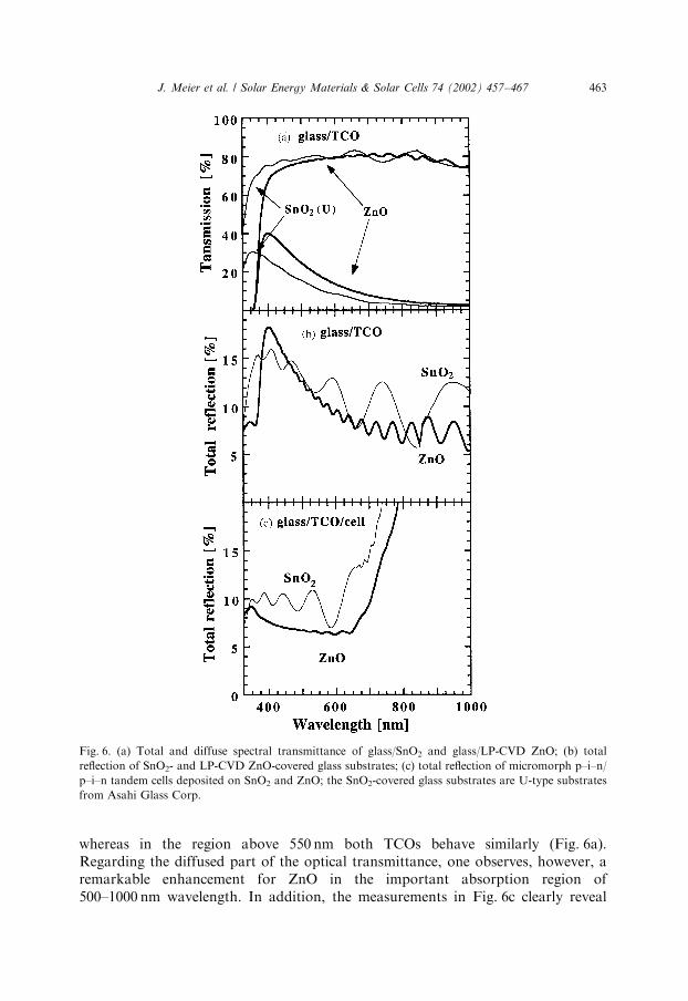
whereas in the region above 550 nm both TCOs behave similarly (Fig. 6a).Regarding the diffused part of the optical transmittance, one observes, however, aremarkable enhancement for ZnO in the important absorption region of500–1000 nm wavelength. In addition, the measurements in Fig. 6c clearly reveal
Fig. 6. (a) Total and diffuse spectral transmittance of glass/SnO2 and glass/LP-CVD ZnO; (b) total
reflection of SnO2- and LP-CVD ZnO-covered glass substrates; (c) total reflection of micromorph p–i–n/
p–i–n tandem cells deposited on SnO2 and ZnO; the SnO2-covered glass substrates are U-type substrates
from Asahi Glass Corp.
J. Meier et al. / Solar Energy Materials & Solar Cells 74 (2002) 457–467 463
that in case of the cells on ZnO a reduced reflection is present compared to SnO2
coated glass substrates. This may be explained by the greater roughness of the ZnO,and further, by a better matched refraction index between the glass and the siliconabsorber. The difference in the reflection characteristics of the two TCOs (Fig. 6c) issupported by the naked eye in a simple manner: in the case of LP-CVD ZnO, themicromorph tandem cell appears as black, whereas in the case of SnO2 themicromorph tandem cell appears to have a brighter color.
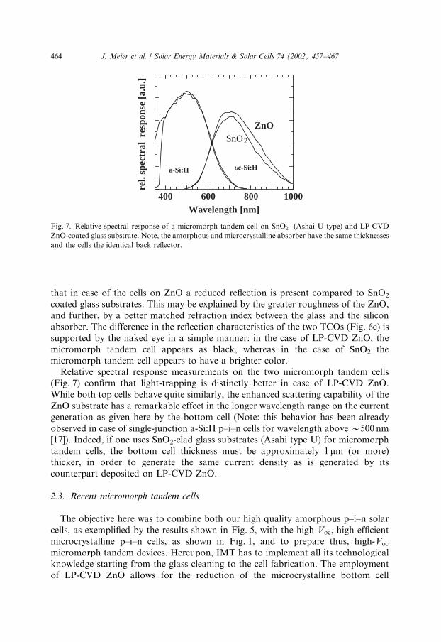
Relative spectral response measurements on the two micromorph tandem cells(Fig. 7) confirm that light-trapping is distinctly better in case of LP-CVD ZnO.While both top cells behave quite similarly, the enhanced scattering capability of theZnO substrate has a remarkable effect in the longer wavelength range on the currentgeneration as given here by the bottom cell (Note: this behavior has been alreadyobserved in case of single-junction a-Si:H p–i–n cells for wavelength above B500 nm[17]). Indeed, if one uses SnO2-clad glass substrates (Asahi type U) for micromorphtandem cells, the bottom cell thickness must be approximately 1 mm (or more)thicker, in order to generate the same current density as is generated by itscounterpart deposited on LP-CVD ZnO.
2.3. Recent micromorph tandem cells
The objective here was to combine both our high quality amorphous p–i–n solarcells, as exemplified by the results shown in Fig. 5, with the high Voc; high efficientmicrocrystalline p–i–n cells, as shown in Fig. 1, and to prepare thus, high-Voc
micromorph tandem devices. Hereupon, IMT has to implement all its technologicalknowledge starting from the glass cleaning to the cell fabrication. The employmentof LP-CVD ZnO allows for the reduction of the microcrystalline bottom cell
SnO2
ZnO
400 600 800 1000
rel.
spec
tral
resp
onse
[a.u
.]
Wavelength [nm]
a-Si:H µc-Si:H
Fig. 7. Relative spectral response of a micromorph tandem cell on SnO2- (Ashai U type) and LP-CVD
ZnO-coated glass substrate. Note, the amorphous and microcrystalline absorber have the same thicknesses
and the cells the identical back reflector.
J. Meier et al. / Solar Energy Materials & Solar Cells 74 (2002) 457–467464
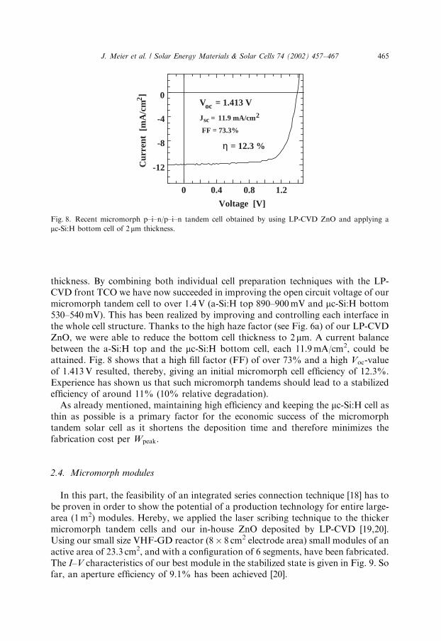
thickness. By combining both individual cell preparation techniques with the LP-CVD front TCO we have now succeeded in improving the open circuit voltage of ourmicromorph tandem cell to over 1.4V (a-Si:H top 890–900mV and mc-Si:H bottom530–540mV). This has been realized by improving and controlling each interface inthe whole cell structure. Thanks to the high haze factor (see Fig. 6a) of our LP-CVDZnO, we were able to reduce the bottom cell thickness to 2 mm. A current balancebetween the a-Si:H top and the mc-Si:H bottom cell, each 11.9mA/cm2, could beattained. Fig. 8 shows that a high fill factor (FF) of over 73% and a high Voc-valueof 1.413V resulted, thereby, giving an initial micromorph cell efficiency of 12.3%.Experience has shown us that such micromorph tandems should lead to a stabilizedefficiency of around 11% (10% relative degradation).
As already mentioned, maintaining high efficiency and keeping the mc-Si:H cell asthin as possible is a primary factor for the economic success of the micromorphtandem solar cell as it shortens the deposition time and therefore minimizes thefabrication cost per Wpeak:
2.4. Micromorph modules
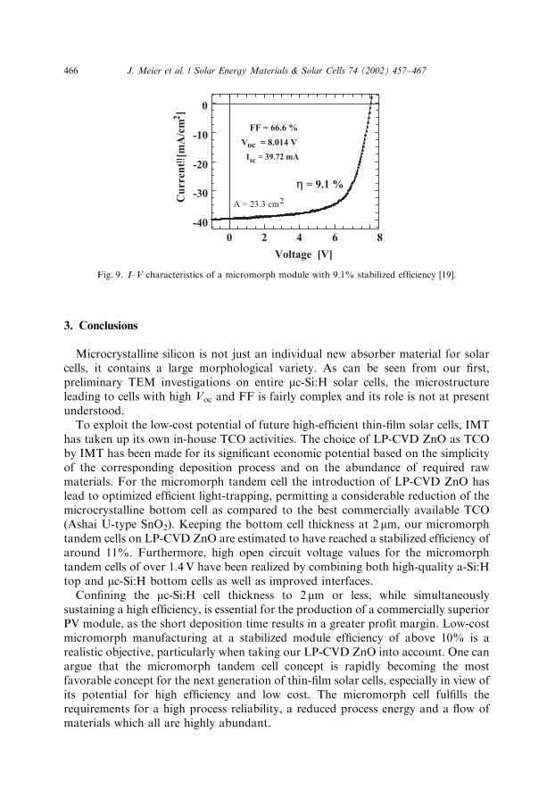
In this part, the feasibility of an integrated series connection technique [18] has tobe proven in order to show the potential of a production technology for entire large-area (1m2) modules. Hereby, we applied the laser scribing technique to the thickermicromorph tandem cells and our in-house ZnO deposited by LP-CVD [19,20].Using our small size VHF-GD reactor (8� 8 cm2 electrode area) small modules of anactive area of 23.3 cm2, and with a configuration of 6 segments, have been fabricated.The I–V characteristics of our best module in the stabilized state is given in Fig. 9. Sofar, an aperture efficiency of 9.1% has been achieved [20].
-12
-8
-4
0
0 0.4 0.8 1.2
Cur
rent
[mA
/cm
2 ]
Voltage [V]
η η = 12.3 %
Voc = 1.413 V
Jsc = 11.9 mA/cm2
FF = 73.3%
Fig. 8. Recent micromorph p–i–n/p–i–n tandem cell obtained by using LP-CVD ZnO and applying a
mc-Si:H bottom cell of 2 mm thickness.
J. Meier et al. / Solar Energy Materials & Solar Cells 74 (2002) 457–467 465
3. Conclusions
Microcrystalline silicon is not just an individual new absorber material for solarcells, it contains a large morphological variety. As can be seen from our first,preliminary TEM investigations on entire mc-Si:H solar cells, the microstructureleading to cells with high Voc and FF is fairly complex and its role is not at presentunderstood.
To exploit the low-cost potential of future high-efficient thin-film solar cells, IMThas taken up its own in-house TCO activities. The choice of LP-CVD ZnO as TCOby IMT has been made for its significant economic potential based on the simplicityof the corresponding deposition process and on the abundance of required rawmaterials. For the micromorph tandem cell the introduction of LP-CVD ZnO haslead to optimized efficient light-trapping, permitting a considerable reduction of themicrocrystalline bottom cell as compared to the best commercially available TCO(Ashai U-type SnO2). Keeping the bottom cell thickness at 2 mm, our micromorphtandem cells on LP-CVD ZnO are estimated to have reached a stabilized efficiency ofaround 11%. Furthermore, high open circuit voltage values for the micromorphtandem cells of over 1.4V have been realized by combining both high-quality a-Si:Htop and mc-Si:H bottom cells as well as improved interfaces.
Confining the mc-Si:H cell thickness to 2 mm or less, while simultaneouslysustaining a high efficiency, is essential for the production of a commercially superiorPV module, as the short deposition time results in a greater profit margin. Low-costmicromorph manufacturing at a stabilized module efficiency of above 10% is arealistic objective, particularly when taking our LP-CVD ZnO into account. One canargue that the micromorph tandem cell concept is rapidly becoming the mostfavorable concept for the next generation of thin-film solar cells, especially in view ofits potential for high efficiency and low cost. The micromorph cell fulfills therequirements for a high process reliability, a reduced process energy and a flow ofmaterials which all are highly abundant.
-40
-30
-20
-10
0
0 2 4 6 8
Cu
rren
t!![
mA
/cm
2]
Voltage [V]
Voc = 8.014 V
A = 23.3 cm2
FF = 66.6 %
η η = 9.1 %
Isc = 39.72 mA
Fig. 9. I–V characteristics of a micromorph module with 9.1% stabilized efficiency [19].
J. Meier et al. / Solar Energy Materials & Solar Cells 74 (2002) 457–467466
Acknowledgements
This work was supported by Swiss Federal Office of Energy BFE/OFEN underContract No. 36487. We are grateful to Dr. K. Emery from the national RenewableEnergy Laboratory for characterization of IMT cells and helpful discussions.
References
[1] J. Meier, R. Fl .uckiger, H. Keppner, A. Shah, Appl. Phys. Lett. 65 (1994) 860.
[2] J. Meier, S. Dubail, R. Fl .uckiger, D. Fischer, H. Keppner, A. Shah, Proceedings of the First
WCPEC, 1994, p. 409.
[3] J. Meier, S. Dubail, J. Cuperus, U. Kroll, R. Platz, P. Torres, J.A. Anna Selvan, P. Pernet, N. Beck,
Pellaton, N. Vaucher, Ch. Hof, D. Fischer, H. Keppner, A. Shah, J. Non-Cryst. Solids 227–230
(1998) 1250.
[4] H. Keppner, J. Meier, P. Torres, D. Fischer, A. Shah, Appl. Phys. A 69 (1999) 169–177.
[5] K. Yamamoto, et al., J. Non-Cryst. Solids 266–269 (1–3) (2000) 1082–1087.
[6] K. Saito, M. Sano, K. Matuda, T. Kondo, T. Nishimoto, K. Ogawa, I. Kajita, Proceedings of the
Second WCPEC, 1998, p. 351.
[7] K. Yamamoto, T. Suzuki, M. Yoshimi, A. Nakajima, Proceedings of the 14th EU PVSEC, 1997,
p. 1018.
[8] K. Yamamoto, M. Yoshimi, T. Suzuki, T. Nakata, T. Sawada, A. Nakajima, K. Hayashi,
Proceedings of the 28th IEEE PVSC, 2000, p. 1428.
[9] K. Yamamoto, M. Yoshimi, T. Suzuki, Y. Tawada, Y. Okamoto, A. Nakajima, Proceedings of the
Second WCPEC, 1998, p. 1284.
[10] O. Vetterl, et al. Proc. Mater. Res. Soc. Symp. 609 (2000) A15.2.1; www.mrs.org
[11] Y. Nasuno, M. Kondo, A. Matsuda, Proceedings of the 28th IEEE PVSC, 2000, p. 142.
[12] S.J. Jones, R. Crucet, M. Izu, Proceedings of the 28th IEEE PVSC, 2000, p. 134.
[13] J. Dubail, et al. Proc.Mater. Res. Soc. Symp. 609 (2000) A13.6.1; www.mrs.org.
[14] E. Vallat-Sauvain, U. Kroll, J. Meier, A. Shah, J. Pohl, J. Appl. Phys. 87 (2000) 3137.
[15] J. Bailat, E. Vallat-Sauvain, L. Feitknecht, A. Shah, J. Non-Cryst. Solids 299–302 (2001) 1219.
[16] S. Fa.y, S. Dubail, U. Kroll, J. Meier, Y. Ziegler, A. Shah, Proceedings of the 16th EU PVSEC, 2000,
p. 361.
[17] J. Meier, U. Kroll, S. Dubail, S. Golay, S. Fa.y, J. Dubail, A. Shah, Proceedings of the 28th IEEE
PVSC, 2000, p. 746.
[18] D. Carlson, et al. Proceedings of the 25th IEEE PVSC, 1996, p. 1023.
[19] S. Golay, J. Meier, S. Dubail, U. Kroll, A. Shah, Proceedings of the 16th EU EPVSEC, 2000, p. 494.
[20] S. Golay, J. Meier, S. Dubail, S. Fa.y, U. Kroll, A. Shah, Proceedings of the 28th IEEE PVSC, 2000,
p. 1456.
J. Meier et al. / Solar Energy Materials & Solar Cells 74 (2002) 457–467 467