Embed Size (px)
Citation preview
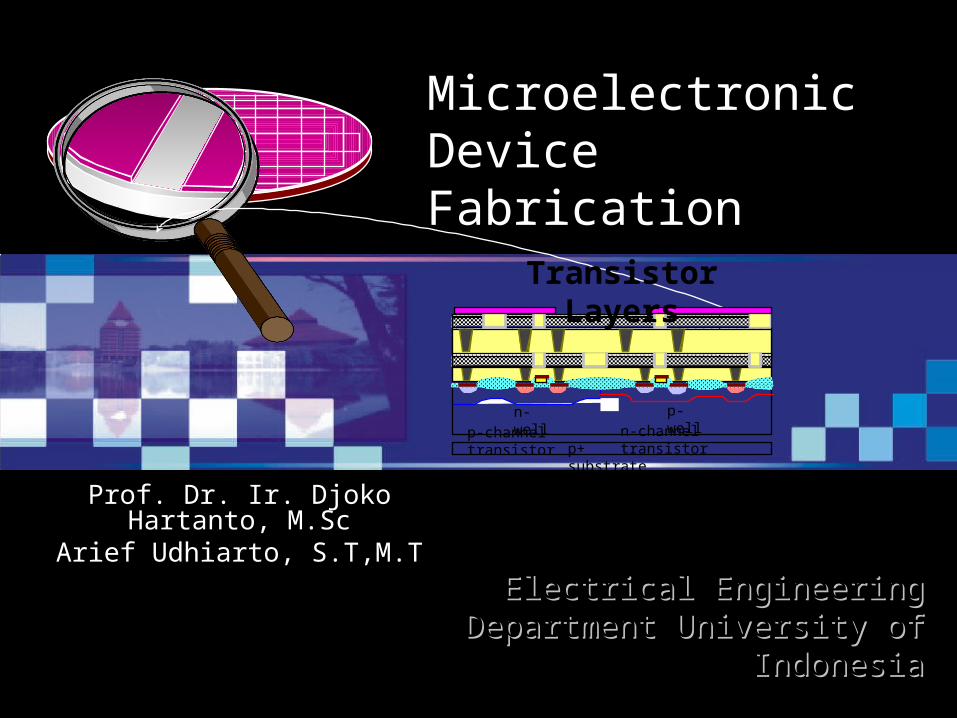
n-well
p-channel transistor
p-well
n-channel transistorp+ substrate
Transistor Layers
Microelectronic Device Microelectronic Device FabricationFabrication
Prof. Dr. Ir. Djoko Hartanto, M.ScProf. Dr. Ir. Djoko Hartanto, M.ScArief Udhiarto, S.T,M.TArief Udhiarto, S.T,M.T
Electrical Engineering Department Electrical Engineering Department University of IndonesiaUniversity of Indonesia
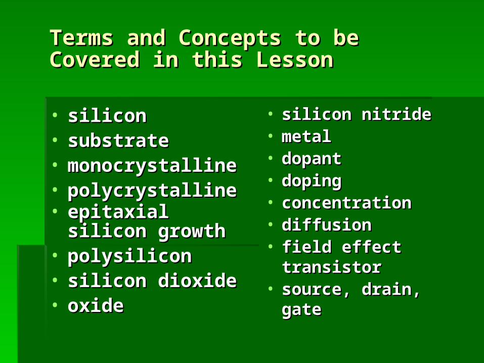
Terms and Concepts to be Terms and Concepts to be Covered in this LessonCovered in this Lesson
• siliconsilicon• substratesubstrate• monocrystallinemonocrystalline• polycrystallinepolycrystalline• epitaxial silicon epitaxial silicon
growthgrowth• polysiliconpolysilicon• silicon dioxide silicon dioxide • oxideoxide
• silicon nitridesilicon nitride• metalmetal• dopantdopant• dopingdoping• concentrationconcentration• diffusiondiffusion• field effect field effect
transistortransistor• source, drain, gatesource, drain, gate

Terms and Concepts to be Terms and Concepts to be Covered in this LessonCovered in this Lesson
• MOSMOS• NMOS technologyNMOS technology• n-channeln-channel• PMOS technologyPMOS technology• p-channelp-channel• CMOS technologyCMOS technology• p-wellp-well• n-welln-well• photoresistphotoresist• photomaskphotomask
• exposureexposure• diffusiondiffusion• thin filmsthin films• photolithographyphotolithography• etchetch• ion implantion implant• polish, CMPpolish, CMP• planarizationplanarization• strips and cleansstrips and cleans• test and sorttest and sort

Variations in Dopant Variations in Dopant ConcentrationsConcentrations
Concentration P-type N-type
lightly doped p- n-
very lightly doped p-- n--
heavily doped p+ n+
very heavily doped p++ n++
Processing OverviewProcessing Overview
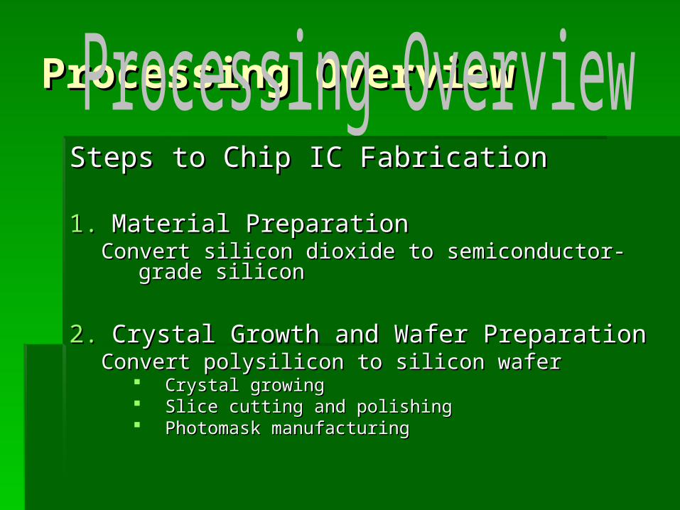
Steps to Chip IC FabricationSteps to Chip IC Fabrication
1.1. Material PreparationMaterial PreparationConvert silicon dioxide to semiconductor-grade siliconConvert silicon dioxide to semiconductor-grade silicon
2.2. Crystal Growth and Wafer Preparation Crystal Growth and Wafer Preparation Convert polysilicon to silicon waferConvert polysilicon to silicon wafer
Crystal growingCrystal growing Slice cutting and polishingSlice cutting and polishing Photomask manufacturingPhotomask manufacturing
Procesing OverviewProcesing Overview
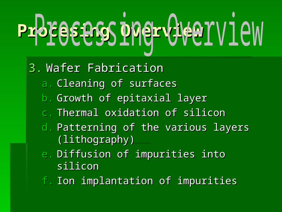
3.3. Wafer FabricationWafer Fabricationa.a. Cleaning of surfacesCleaning of surfaces
b.b. Growth of epitaxial layerGrowth of epitaxial layer
c.c. Thermal oxidation of siliconThermal oxidation of silicon
d.d. Patterning of the various layers Patterning of the various layers (lithography)(lithography)
e.e. Diffusion of impurities into siliconDiffusion of impurities into silicon
f.f. Ion implantation of impuritiesIon implantation of impurities
77
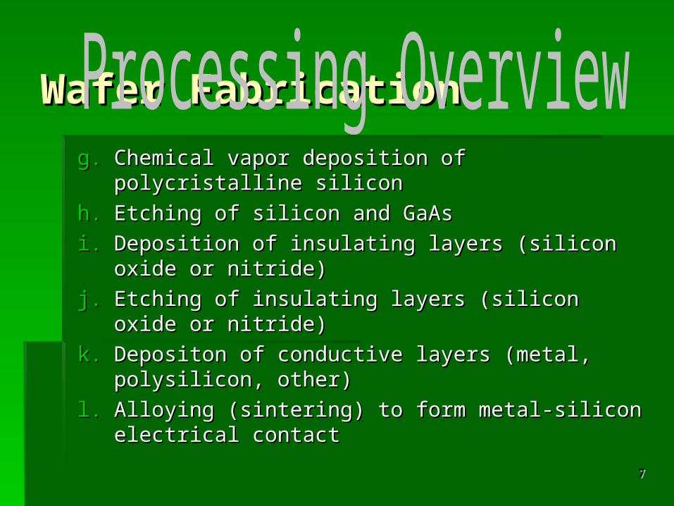
Wafer FabricationWafer Fabrication
g.g. Chemical vapor deposition of polycristalline siliconChemical vapor deposition of polycristalline silicon
h.h. Etching of silicon and GaAsEtching of silicon and GaAs
i.i. Deposition of insulating layers (silicon oxide or Deposition of insulating layers (silicon oxide or nitride)nitride)
j.j. Etching of insulating layers (silicon oxide or nitride)Etching of insulating layers (silicon oxide or nitride)
k.k. Depositon of conductive layers (metal, polysilicon, Depositon of conductive layers (metal, polysilicon, other)other)
l.l. Alloying (sintering) to form metal-silicon electrical Alloying (sintering) to form metal-silicon electrical contactcontact
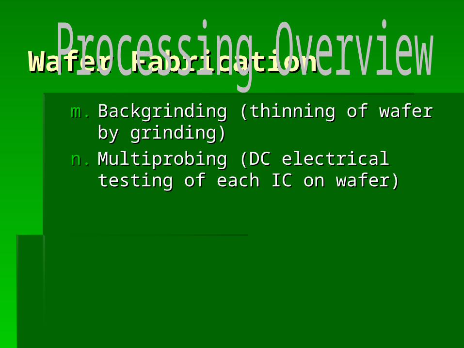
Wafer FabricationWafer Fabrication
m.m. Backgrinding (thinning of wafer by Backgrinding (thinning of wafer by grinding)grinding)
n.n. Multiprobing (DC electrical testing of each Multiprobing (DC electrical testing of each IC on wafer)IC on wafer)
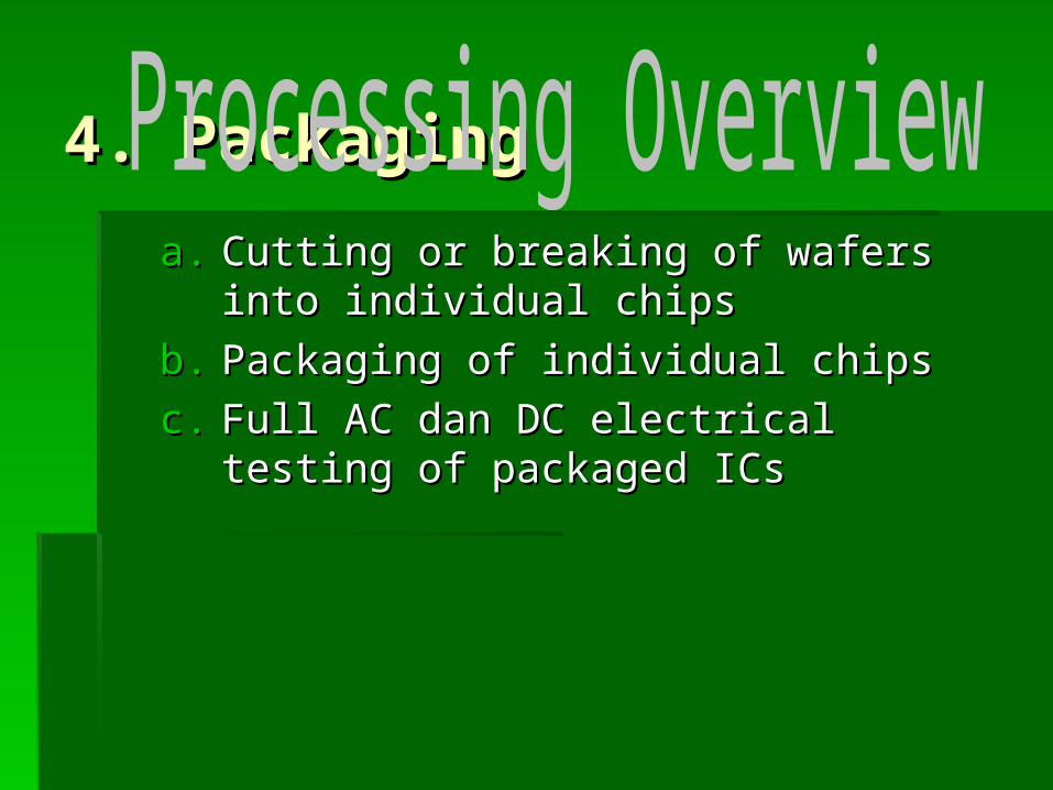
4. Packaging4. Packaging
a.a. Cutting or breaking of wafers into individual Cutting or breaking of wafers into individual chipschips
b.b. Packaging of individual chipsPackaging of individual chips
c.c. Full AC dan DC electrical testing of Full AC dan DC electrical testing of packaged ICspackaged ICs
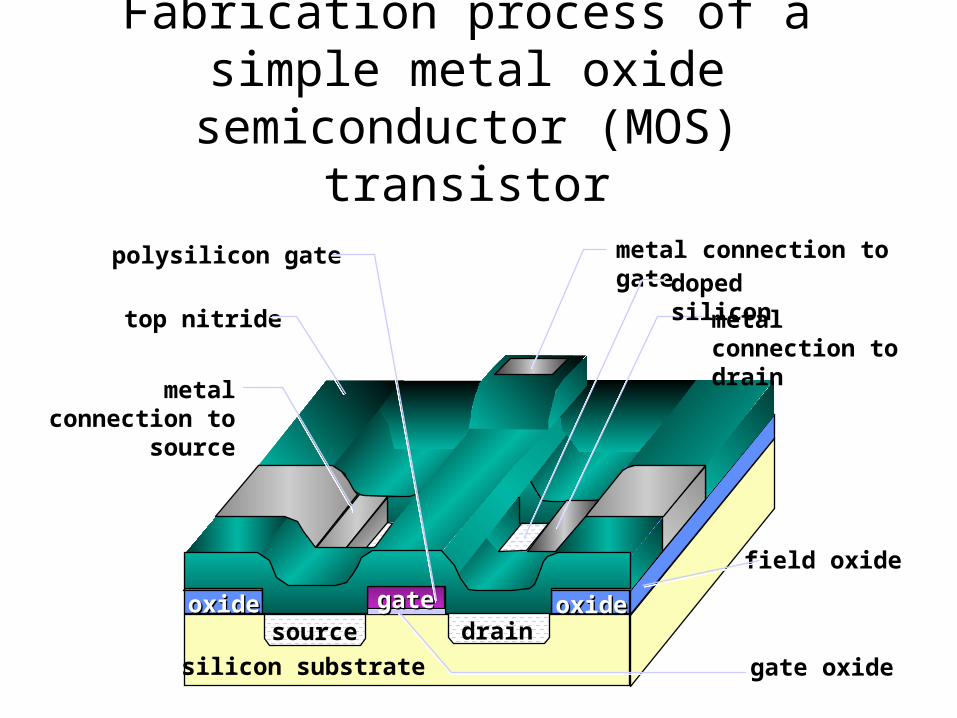
Fabrication process of a simple metal oxide semiconductor (MOS) transistor
silicon substrate
source draingategateoxideoxide oxideoxide
top nitride
metal connection to source
metal connection to gate
metal connection to drain
polysilicon gatedoped silicon
field oxide
gate oxide

The manufacture of a single MOS transistor begins with a silicon substrate.
silicon substrate
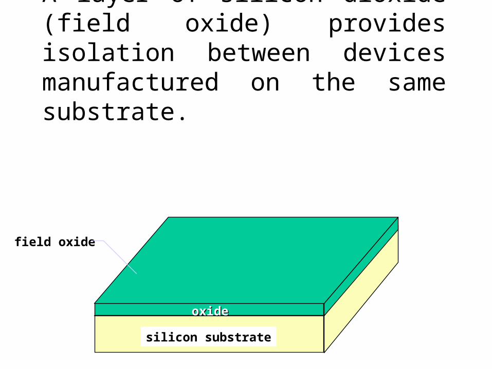
A layer of silicon dioxide (field oxide) provides isolation between devices manufactured on the same substrate.
silicon substrate
oxideoxide
field oxide
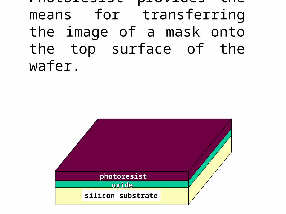
Photoresist provides the means for transferring the image of a mask onto the top surface of the wafer.
silicon substrate
oxideoxidephotoresistphotoresist

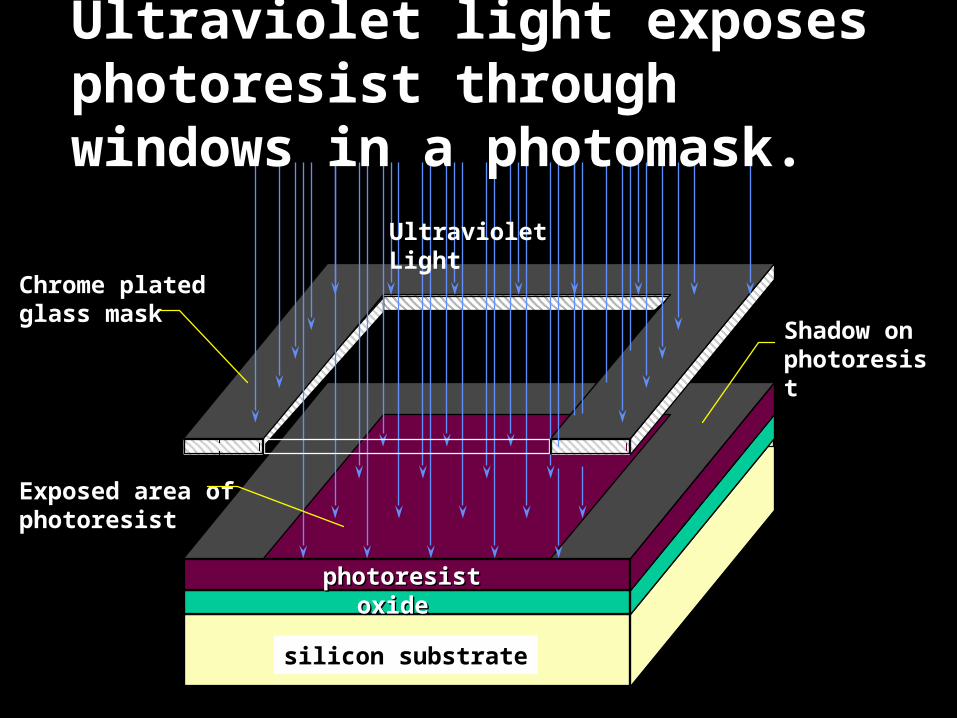
Shadow on photoresist
photoresistphotoresist
Exposed area of photoresist
Chrome platedglass mask
Ultraviolet Light
silicon substrate
oxideoxide
Ultraviolet light exposes photoresist through windows in a photomask.
Shadow on photoresist
photoresistphotoresist
Exposed area of photoresist
Chrome platedglass mask
Ultraviolet Light
silicon substrate
oxideoxide
Ultraviolet light exposes photoresist through windows in a photomask.
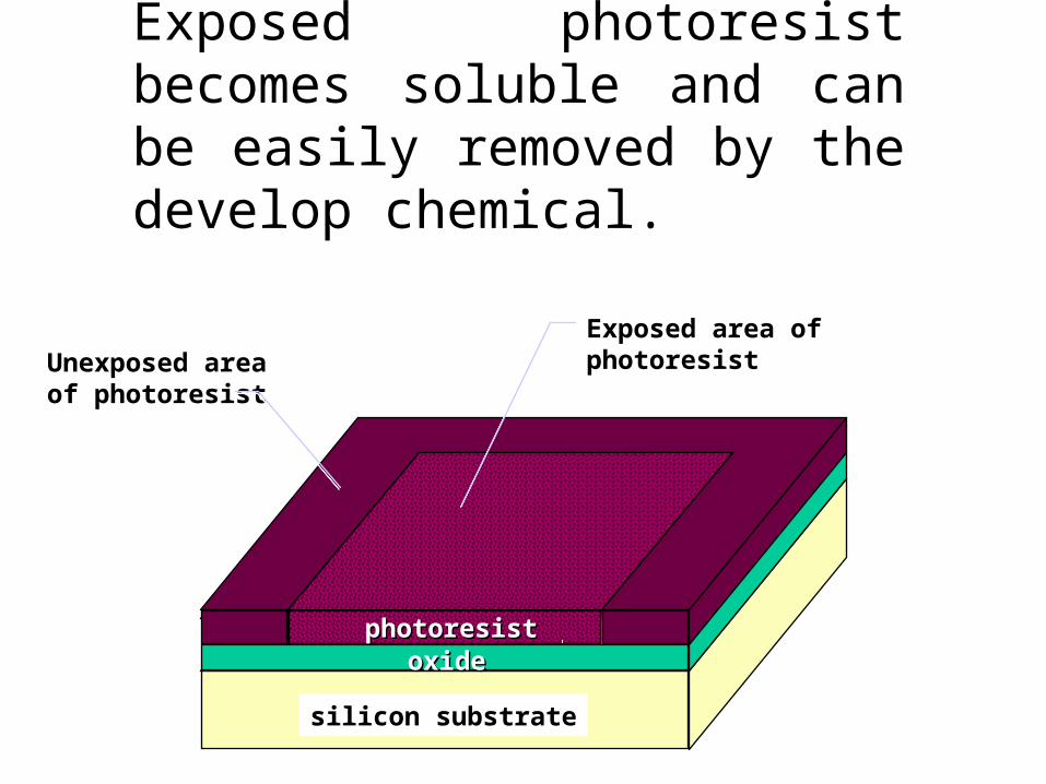
Exposed photoresist becomes soluble and can be easily removed by the develop chemical.
Unexposed area of photoresist
silicon substrate
Exposed area of photoresist
oxideoxidephotoresistphotoresist
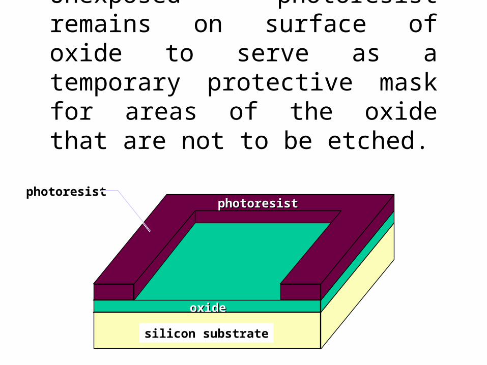
Unexposed photoresist remains on surface of oxide to serve as a temporary protective mask for areas of the oxide that are not to be etched.
Shadow on photoresist
silicon substrate
oxideoxide
photoresistphotoresistphotoresist

Areas of oxide protected by photoresist remain on the silicon substrate while exposed oxide is removed by the etching process.
silicon substrate
oxideoxide oxideoxide
silicon substrate
photoresistphotoresist
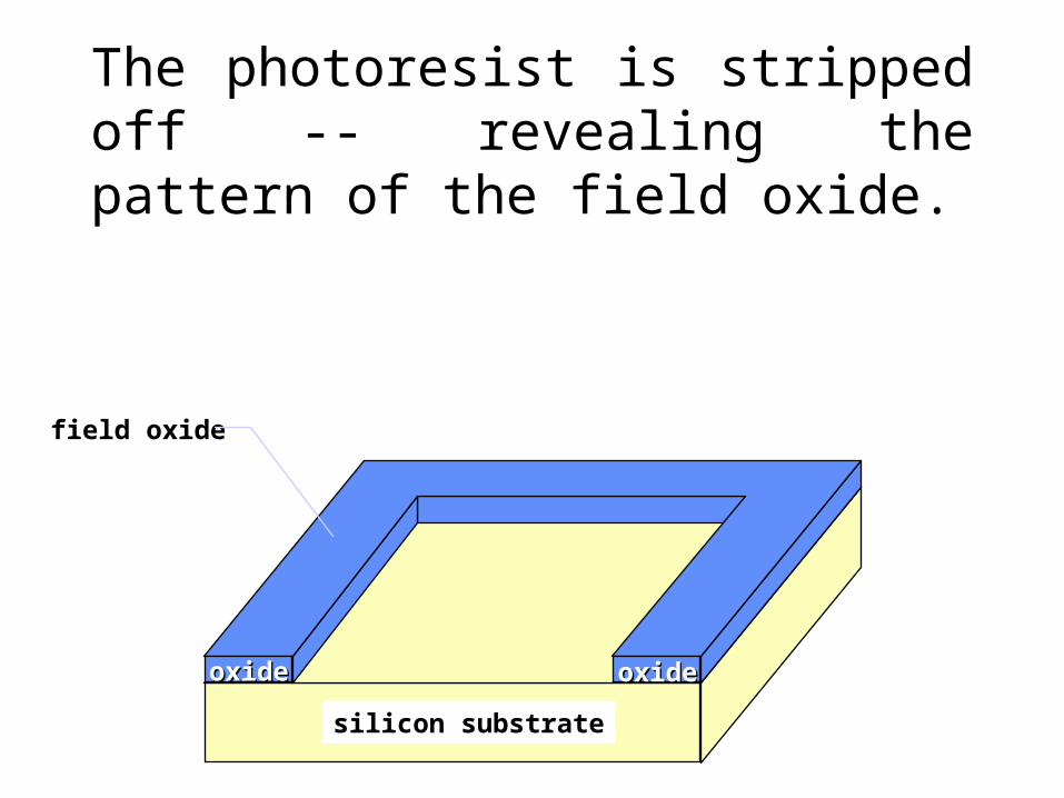
The photoresist is stripped off -- revealing the pattern of the field oxide.
silicon substrate
oxideoxide oxideoxide
silicon substrate
field oxide
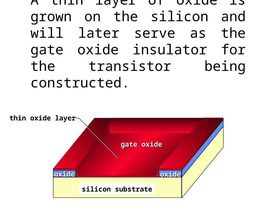
A thin layer of oxide is grown on the silicon and will later serve as the gate oxide insulator for the transistor being constructed.
silicon substrate
oxideoxide oxideoxide
gate oxidegate oxide
thin oxide layer
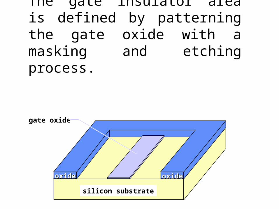
The gate insulator area is defined by patterning the gate oxide with a masking and etching process.
silicon substrate
oxideoxide oxideoxide
gate oxide
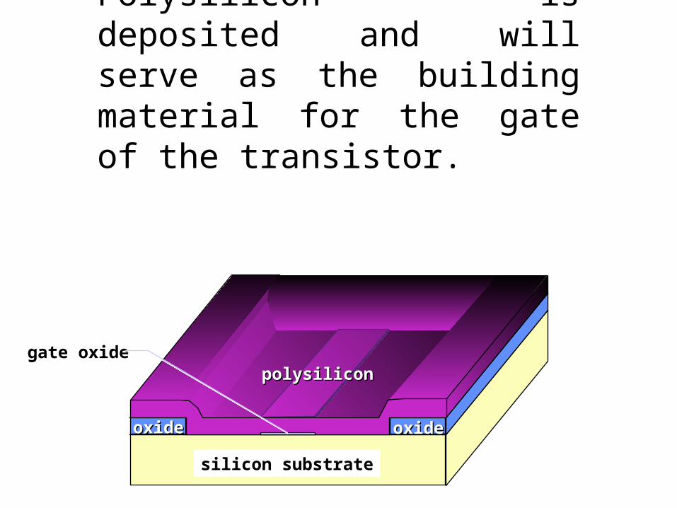
Polysilicon is deposited and will serve as the building material for the gate of the transistor.
silicon substrate
oxideoxide oxideoxide
gate oxide
polysiliconpolysilicongate oxide
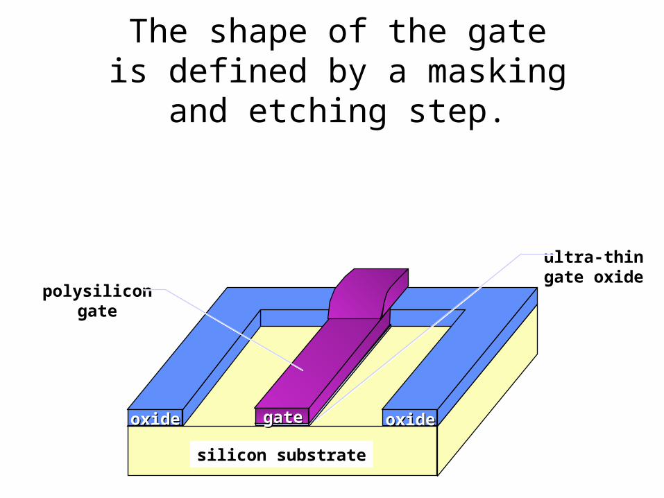
The shape of the gate is defined by a masking and etching step.
silicon substrate
oxideoxide oxideoxidegategategate
ultra-thin gate oxide
polysilicongate
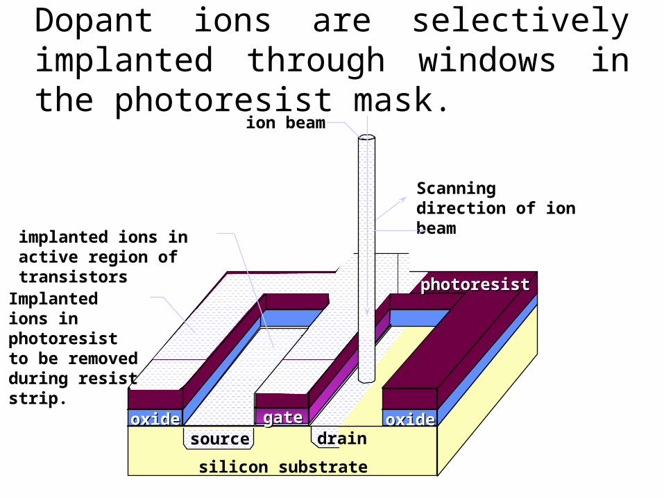
Dopant ions are selectively implanted through windows in the photoresist mask.
silicon substrate
oxideoxide oxideoxidegategategate
photoresistphotoresist
Scanning direction of ion beam
implanted ions in active region of transistors
Implanted ions in photoresist to be removed during resist strip.
source drain
ion beam
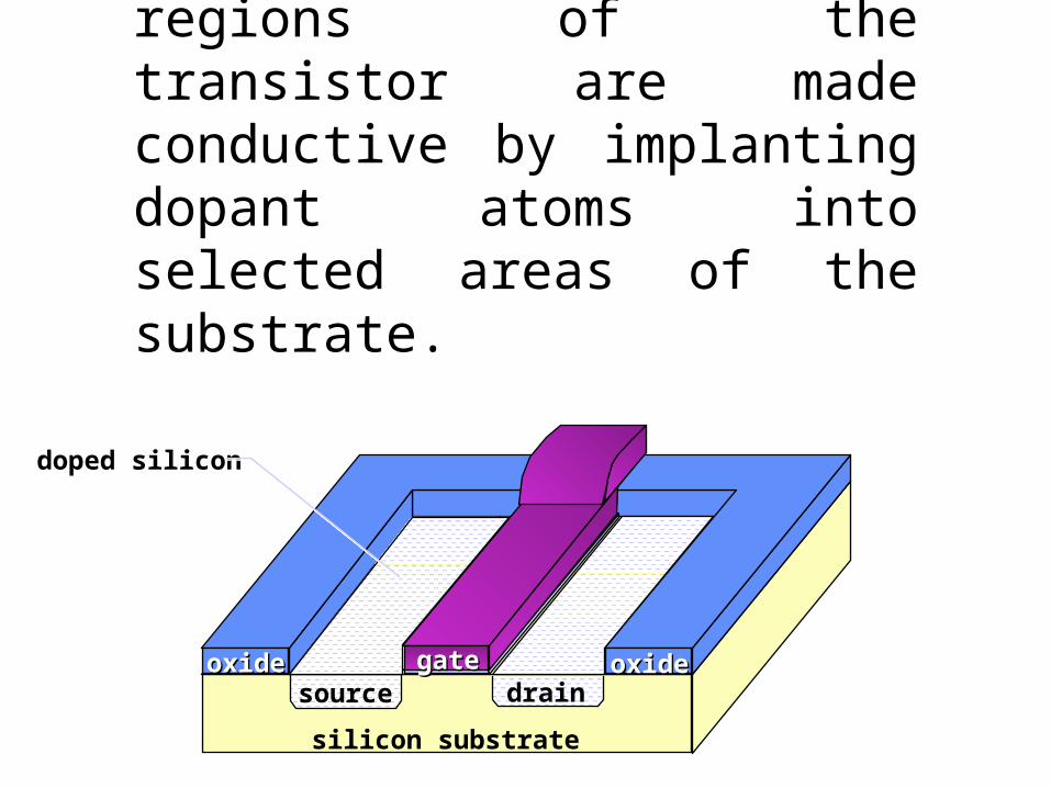
The source and drain regions of the transistor are made conductive by implanting dopant atoms into selected areas of the substrate.
silicon substrate
oxideoxide oxideoxidegategategate
source drain
doped silicon
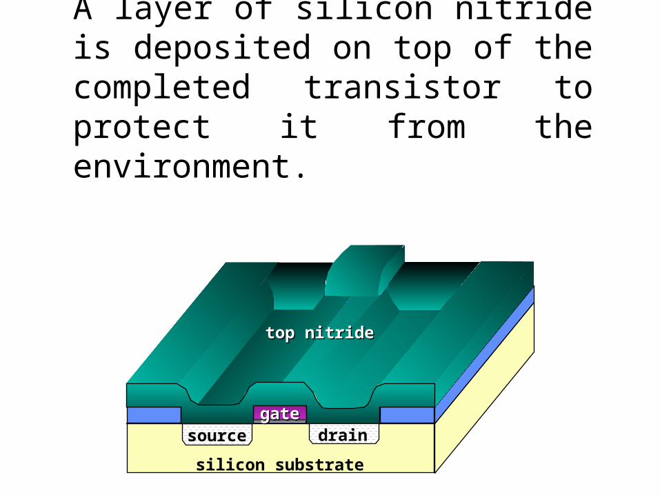
A layer of silicon nitride is deposited on top of the completed transistor to protect it from the environment.
silicon substrate
source draingategate
top nitridetop nitride
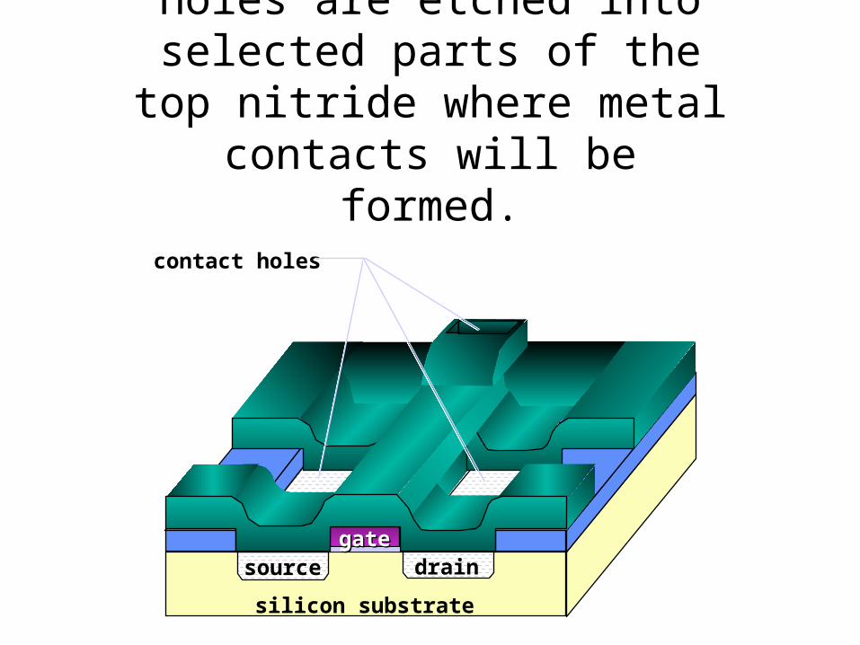
Holes are etched into selected parts of the top nitride where
metal contacts will be formed.
silicon substrate
source draingategate
contact holes
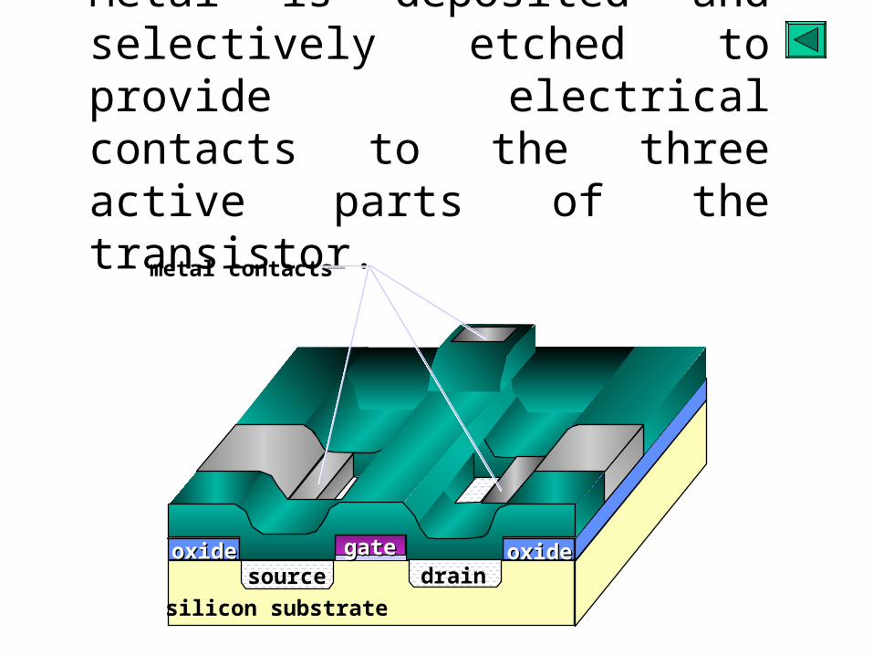
Metal is deposited and selectively etched to provide electrical contacts to the three active parts of the transistor.
silicon substrate
source draingategateoxideoxide oxideoxide
metal contacts
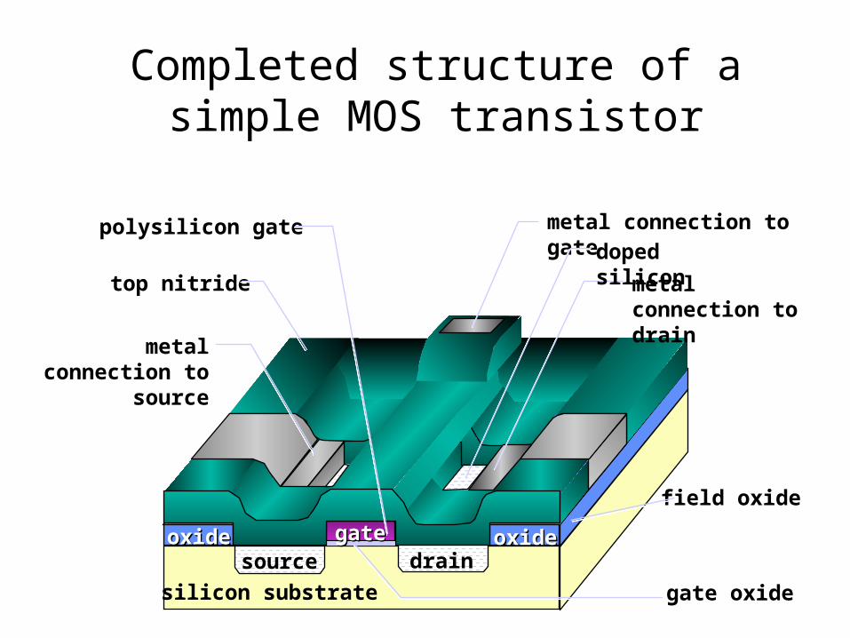
Completed structure of a simple MOS transistor
silicon substrate
source draingategateoxideoxide oxideoxide
top nitride
metal connection to source
metal connection to gate
metal connection to drain
polysilicon gatedoped silicon
field oxide
gate oxide
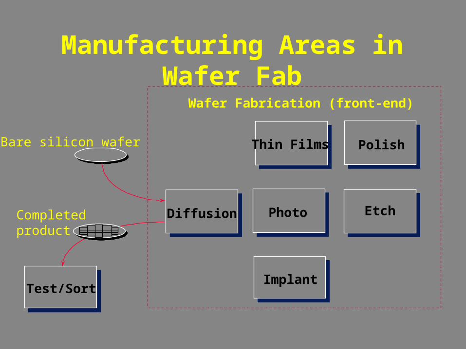
Test/Sort
Thin Films
Photo
Implant
Diffusion Etch
Polish
Manufacturing Areas in Wafer Fab
Wafer Fabrication (front-end)
Bare silicon wafer
Completed product
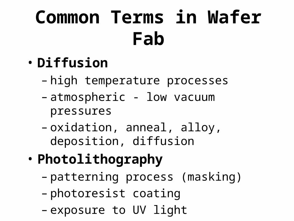
Common Terms in Wafer Fab
• Diffusion– high temperature processes– atmospheric - low vacuum pressures– oxidation, anneal, alloy, deposition, diffusion
• Photolithography– patterning process (masking)– photoresist coating– exposure to UV light– develop
Common Terms in Wafer Fab
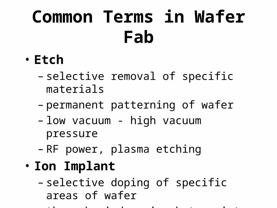
• Etch– selective removal of specific materials– permanent patterning of wafer– low vacuum - high vacuum pressure– RF power, plasma etching
• Ion Implant– selective doping of specific areas of wafer– through windows in photoresist or oxide– high voltage, high vacuum, ion acceleration
Common Terms in Wafer Fab
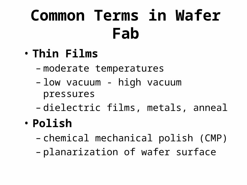
• Thin Films– moderate temperatures– low vacuum - high vacuum pressures– dielectric films, metals, anneal
• Polish– chemical mechanical polish (CMP)– planarization of wafer surface
Common Terms in Wafer Fab
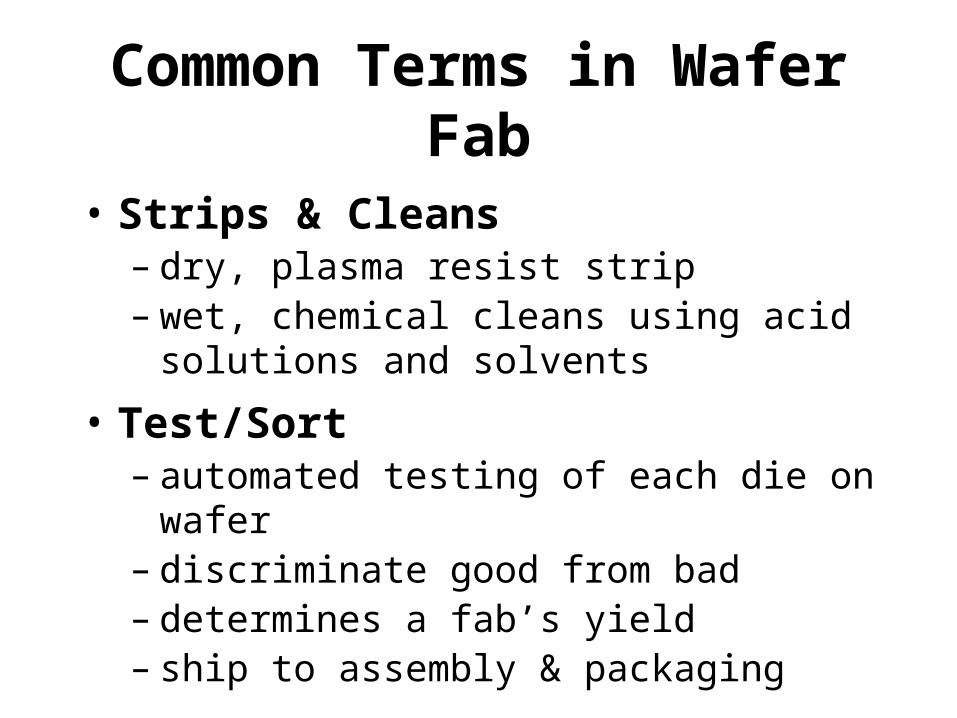
• Strips & Cleans– dry, plasma resist strip– wet, chemical cleans using acid solutions and
solvents
• Test/Sort– automated testing of each die on wafer– discriminate good from bad– determines a fab’s yield– ship to assembly & packaging
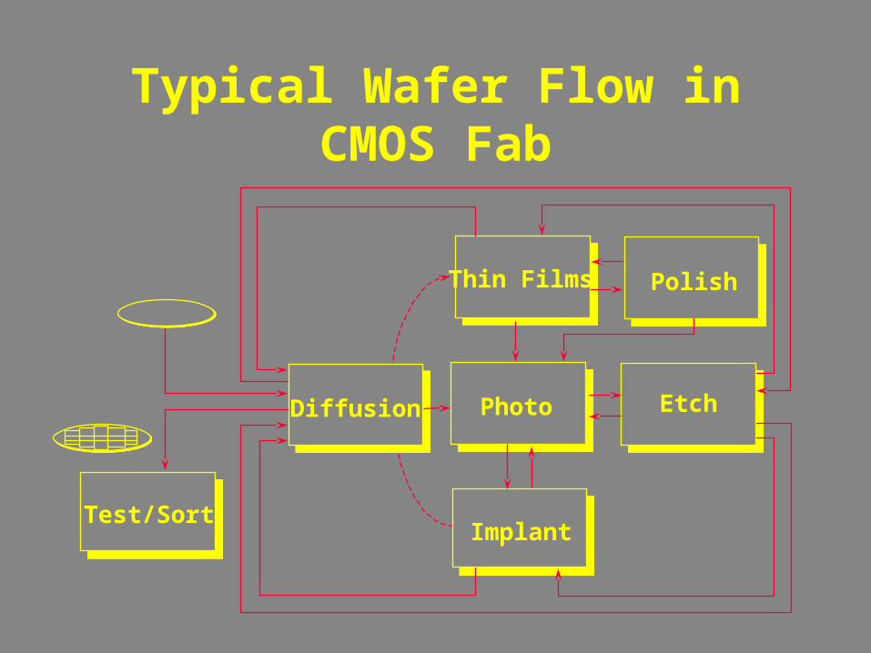
Typical Wafer Flow in CMOS Fab
Thin Films
Photo
Implant
Diffusion Etch
Test/Sort
Polish
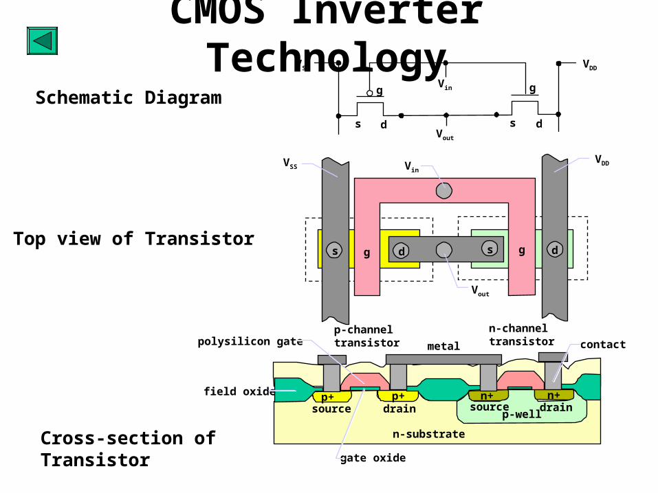
CMOS Inverter Technology
Schematic Diagram
Top view of Transistor
Cross-section of Transistor
VDDVSS
Vout
Vin
s d s d
g g
VDDVSS
Vout
Vin
g gs d s d
n-channel transistor
p-channel transistor
p-well
n+p+ n+p+
n-substrate
source drainsourcedrain
field oxide
gate oxide
metalpolysilicon gate contact