Embed Size (px)
Citation preview
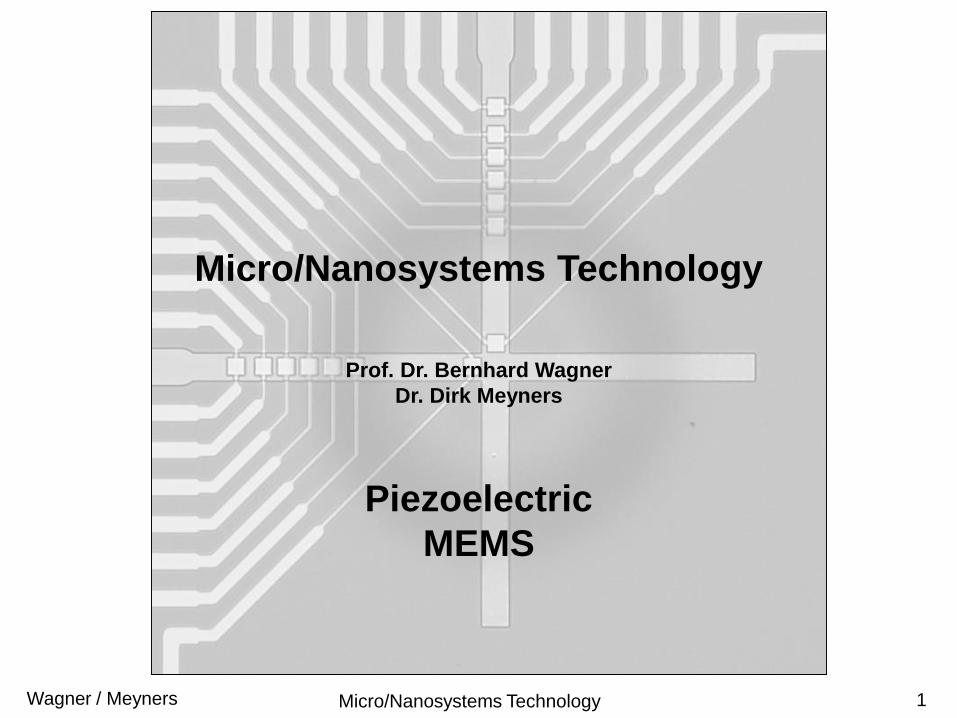
Micro/Nanosystems TechnologyWagner / Meyners 1
Micro/Nanosystems Technology
Prof. Dr. Bernhard Wagner
Dr. Dirk Meyners
Piezoelectric
MEMS

Micro/Nanosystems TechnologyWagner / Meyners 2
Micro/Nanosystems Technology
Prof. Dr. Bernhard Wagner
Dr. Dirk Meyners
Piezoelectric
MEMS
Micro/Nanosystems TechnologyWagner / Meyners 3
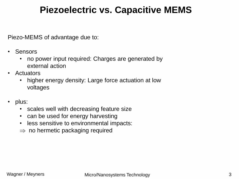
Piezoelectric vs. Capacitive MEMS
Piezo-MEMS of advantage due to:
• Sensors
• no power input required: Charges are generated by
external action
• Actuators
• higher energy density: Large force actuation at low
voltages
• plus:
• scales well with decreasing feature size
• can be used for energy harvesting
• less sensitive to environmental impacts:
no hermetic packaging required
Micro/Nanosystems TechnologyWagner / Meyners 4
Outline
Dielectricity and piezoelectricity
Polarization
Piezoelectric thin films
Piezoelectric thin film materials
Piezo-MEMS
Micro/Nanosystems TechnologyWagner / Meyners 5
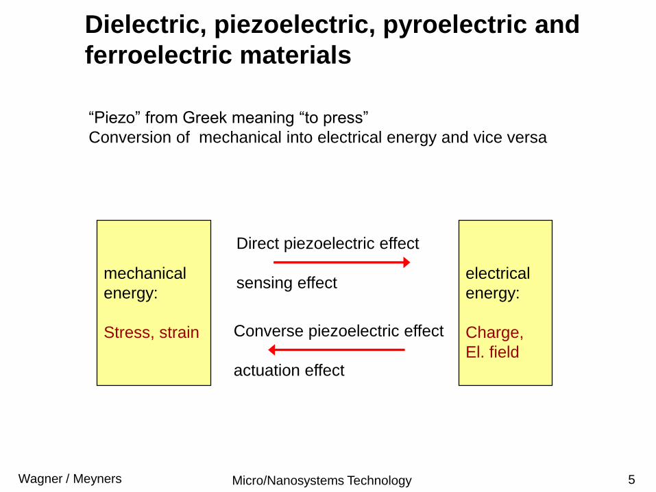
mechanical
energy:
Stress, strain
electrical
energy:
Charge,
El. field
“Piezo” from Greek meaning “to press”
Conversion of mechanical into electrical energy and vice versa
Direct piezoelectric effect
sensing effect
Converse piezoelectric effect
actuation effect
Dielectric, piezoelectric, pyroelectric and
ferroelectric materials
Micro/Nanosystems TechnologyWagner / Meyners 6
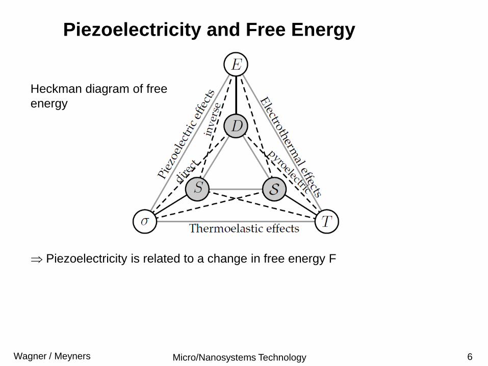
Piezoelectricity and Free Energy
Heckman diagram of free
energy
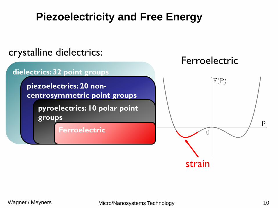
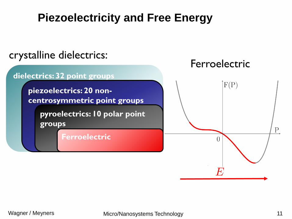
Piezoelectricity is related to a change in free energy F
Micro/Nanosystems TechnologyWagner / Meyners 7
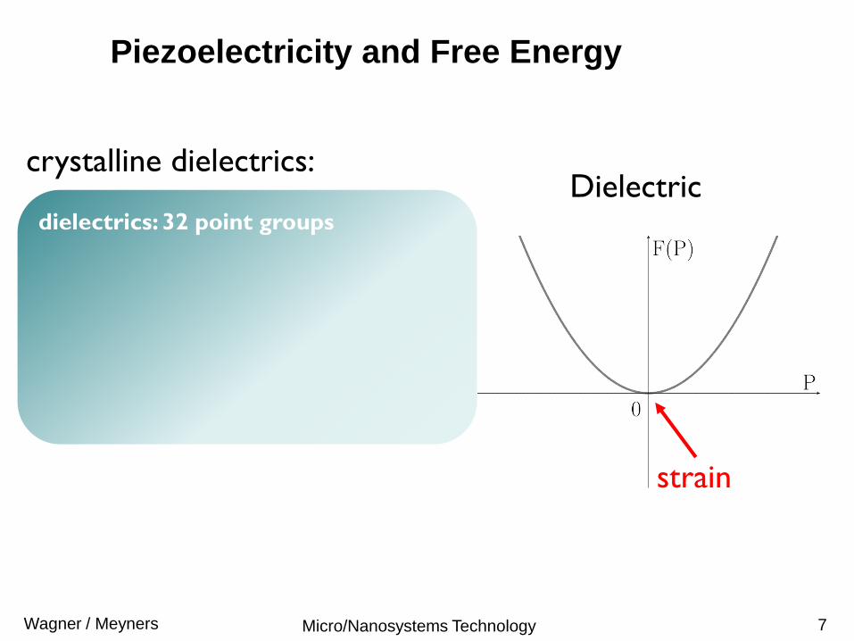
Piezoelectricity and Free Energy
crystalline dielectrics:
dielectrics: 32 point groups
Dielectric
strain
Micro/Nanosystems TechnologyWagner / Meyners 8
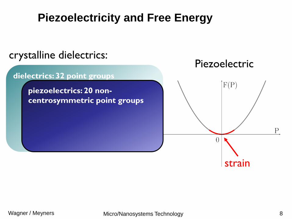
Piezoelectricity and Free Energy
crystalline dielectrics:
dielectrics: 32 point groups
Piezoelectric
strain
piezoelectrics: 20 non-
centrosymmetric point groups
Micro/Nanosystems TechnologyWagner / Meyners 9
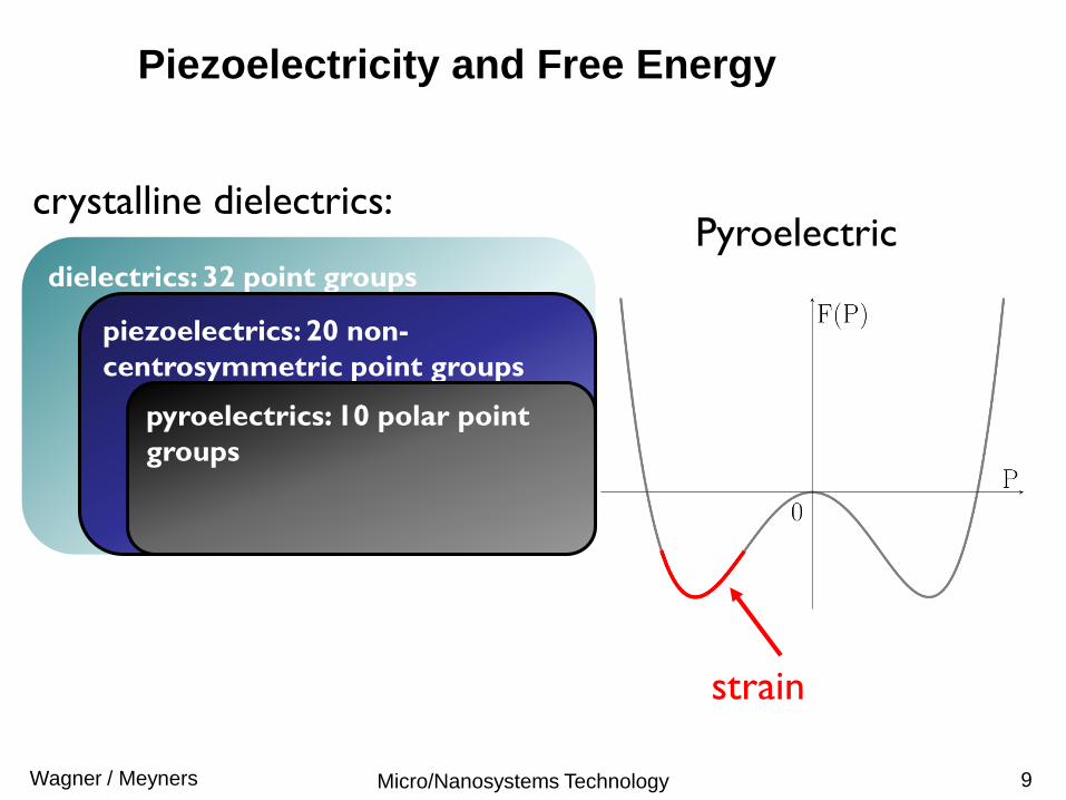
Piezoelectricity and Free Energy
crystalline dielectrics:
dielectrics: 32 point groups
Pyroelectric
strain
piezoelectrics: 20 non-
centrosymmetric point groups
pyroelectrics: 10 polar point
groups
strain
Micro/Nanosystems TechnologyWagner / Meyners 10
Piezoelectricity and Free Energy
crystalline dielectrics:
dielectrics: 32 point groups
Ferroelectric
strain
piezoelectrics: 20 non-
centrosymmetric point groups
pyroelectrics: 10 polar point
groups
Ferroelectric
strain
Micro/Nanosystems TechnologyWagner / Meyners 11
Piezoelectricity and Free Energy
crystalline dielectrics:
dielectrics: 32 point groups
Ferroelectric
strain
piezoelectrics: 20 non-
centrosymmetric point groups
pyroelectrics: 10 polar point
groups
Ferroelectric
Micro/Nanosystems TechnologyWagner / Meyners 12
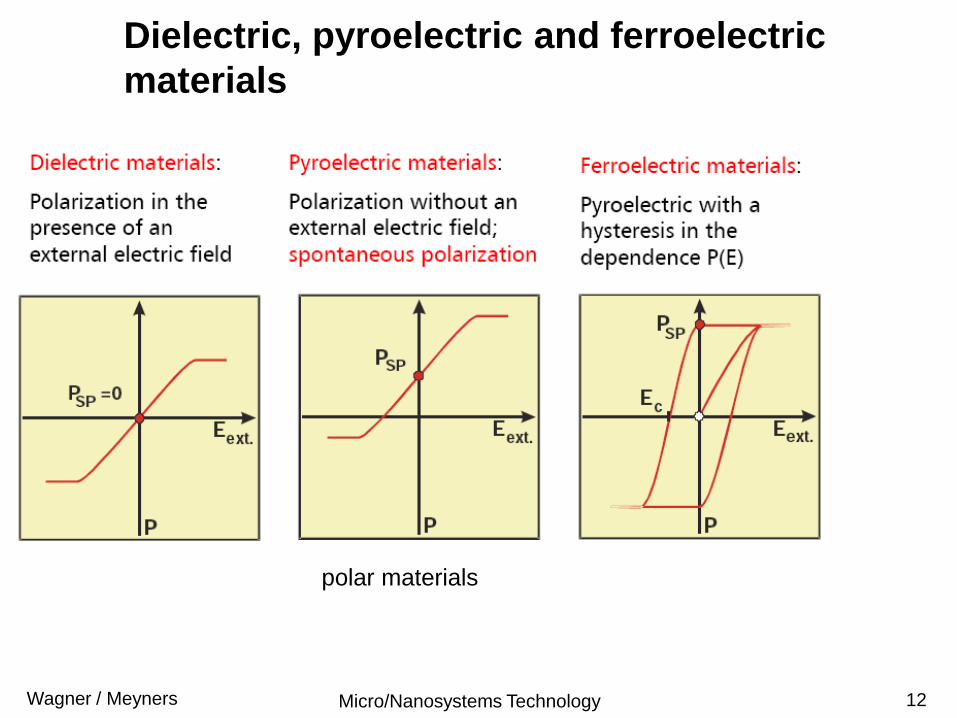
polar materials
Dielectric, pyroelectric and ferroelectric
materials
Micro/Nanosystems TechnologyWagner / Meyners 13
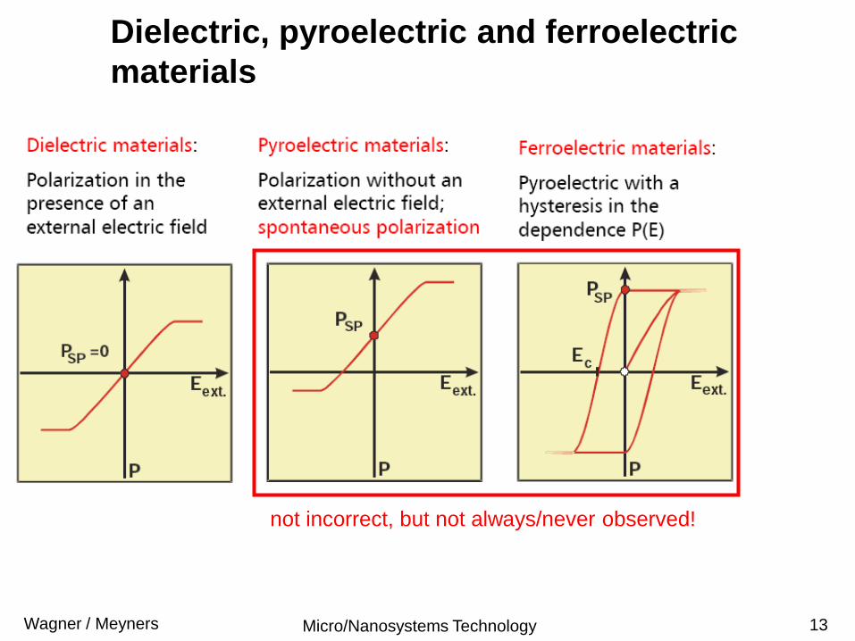
polar materials
Dielectric, pyroelectric and ferroelectric
materials
not incorrect, but not always/never observed!
Micro/Nanosystems TechnologyWagner / Meyners 14
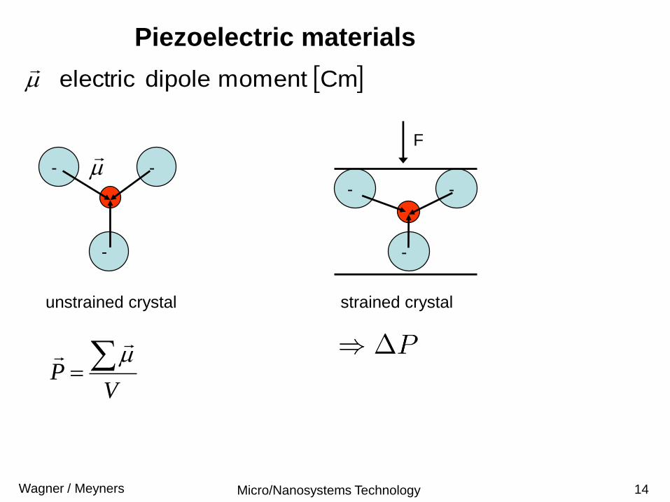
Piezoelectric materials
- -
-
strained crystal
Cm moment dipoleelectric
unstrained crystal
- -
-
F
VP
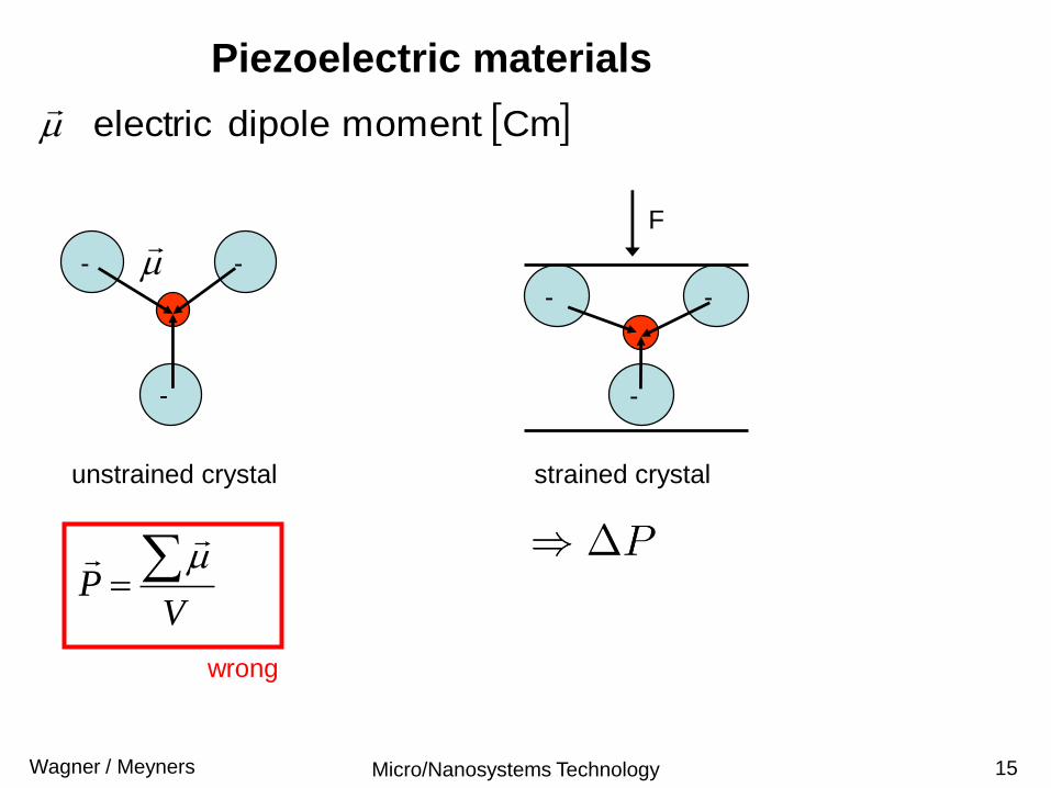
Micro/Nanosystems TechnologyWagner / Meyners 15
Piezoelectric materials
- -
-
strained crystal
Cm moment dipoleelectric
unstrained crystal
- -
-
F
VP
wrong
Micro/Nanosystems TechnologyWagner / Meyners 16
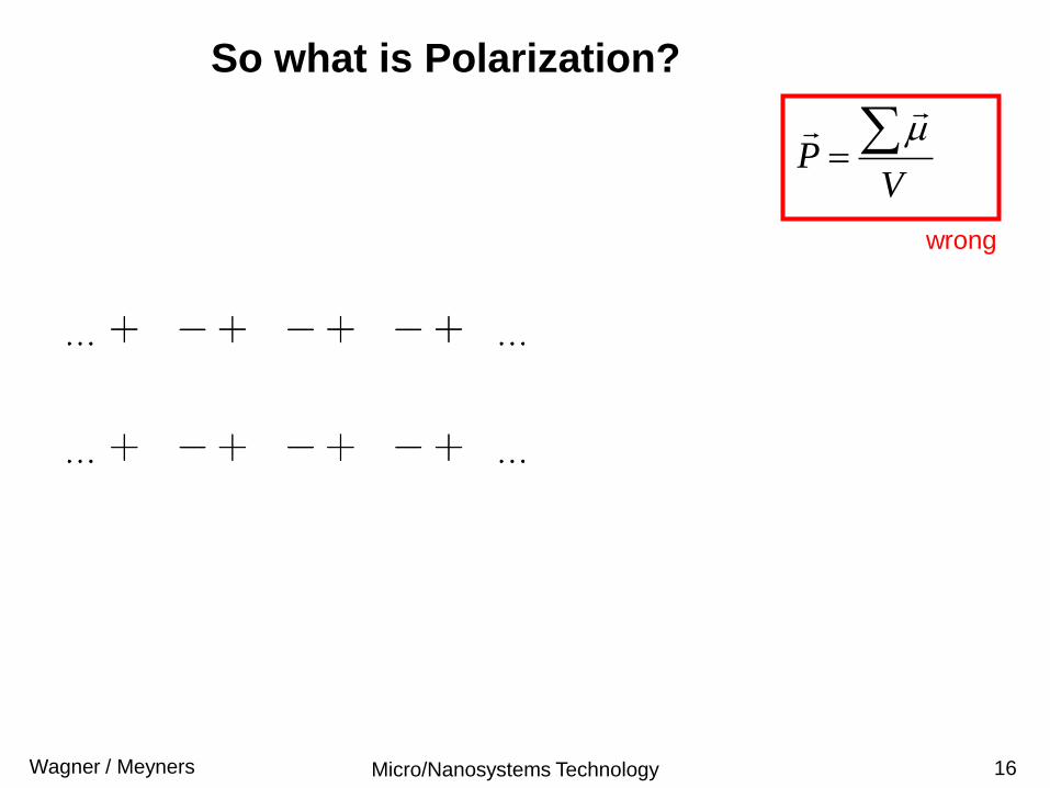
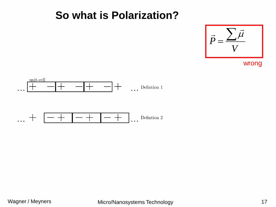
So what is Polarization?
VP
wrong
Micro/Nanosystems TechnologyWagner / Meyners 17
So what is Polarization?
VP
wrong
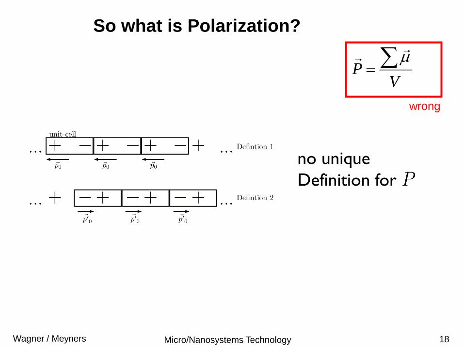
Micro/Nanosystems TechnologyWagner / Meyners 18
So what is Polarization?
VP
wrong
no unique
Definition for
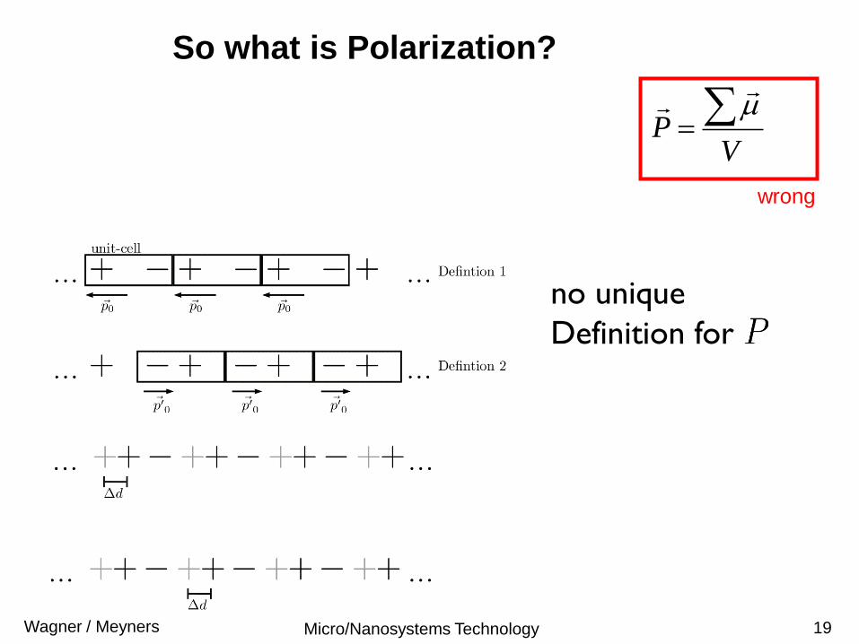
Micro/Nanosystems TechnologyWagner / Meyners 19
So what is Polarization?
VP
wrong
no unique
Definition for
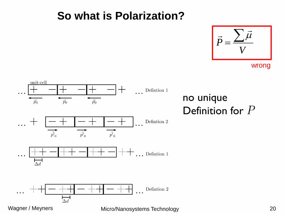
Micro/Nanosystems TechnologyWagner / Meyners 20
So what is Polarization?
VP
wrong
no unique
Definition for
Micro/Nanosystems TechnologyWagner / Meyners 21
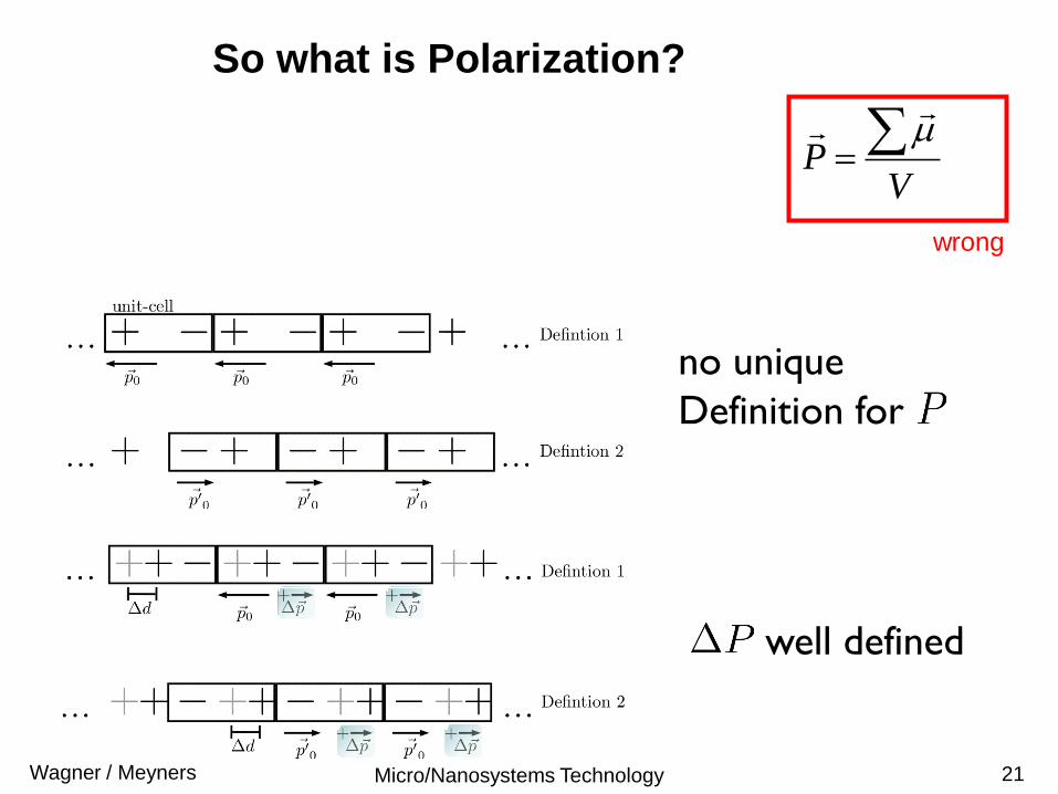
So what is Polarization?
VP
wrong
no unique
Definition for
well defined
Micro/Nanosystems TechnologyWagner / Meyners 22
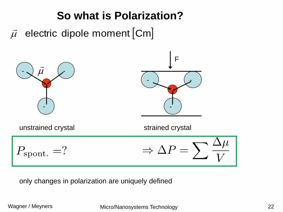
So what is Polarization?
- -
-
strained crystal
Cm moment dipoleelectric
unstrained crystal
- -
-
F
only changes in polarization are uniquely defined
Micro/Nanosystems TechnologyWagner / Meyners 23
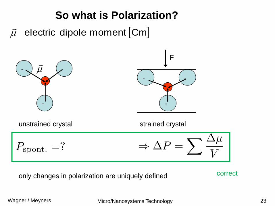
So what is Polarization?
- -
-
strained crystal
Cm moment dipoleelectric
unstrained crystal
- -
-
F
only changes in polarization are uniquely defined correct
Micro/Nanosystems TechnologyWagner / Meyners 24
So what is Polarization?
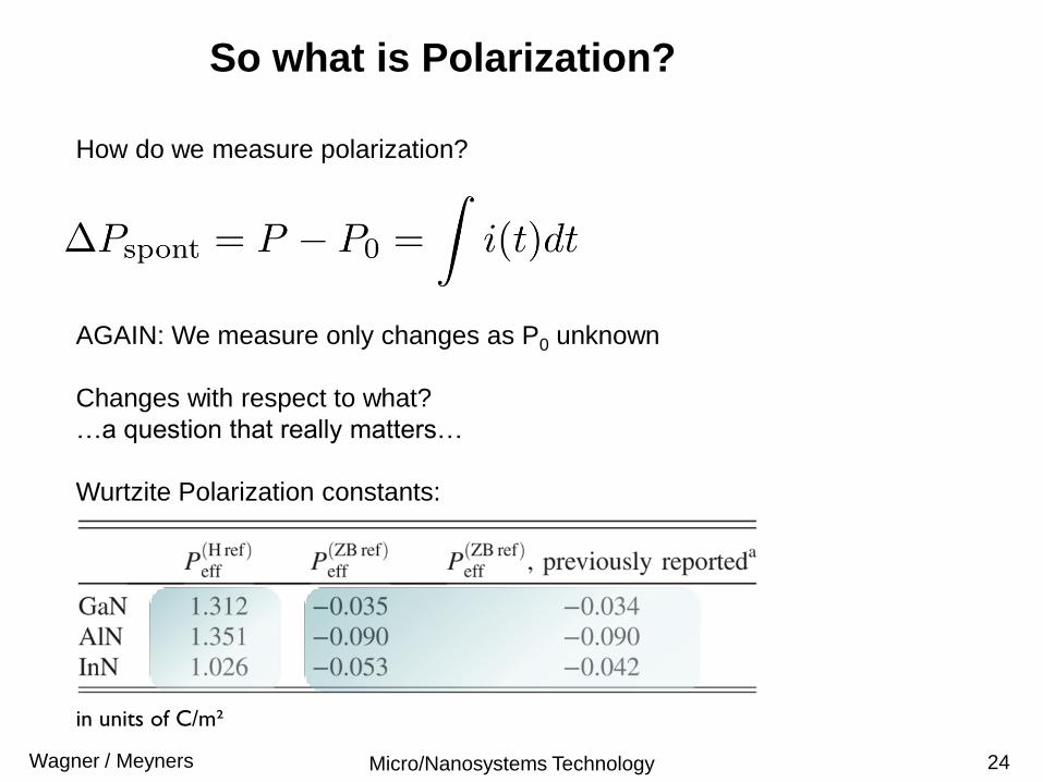
How do we measure polarization?
AGAIN: We measure only changes as P0 unknown
Changes with respect to what?
…a question that really matters…
Wurtzite Polarization constants:
in units of C/m²
Micro/Nanosystems TechnologyWagner / Meyners 25
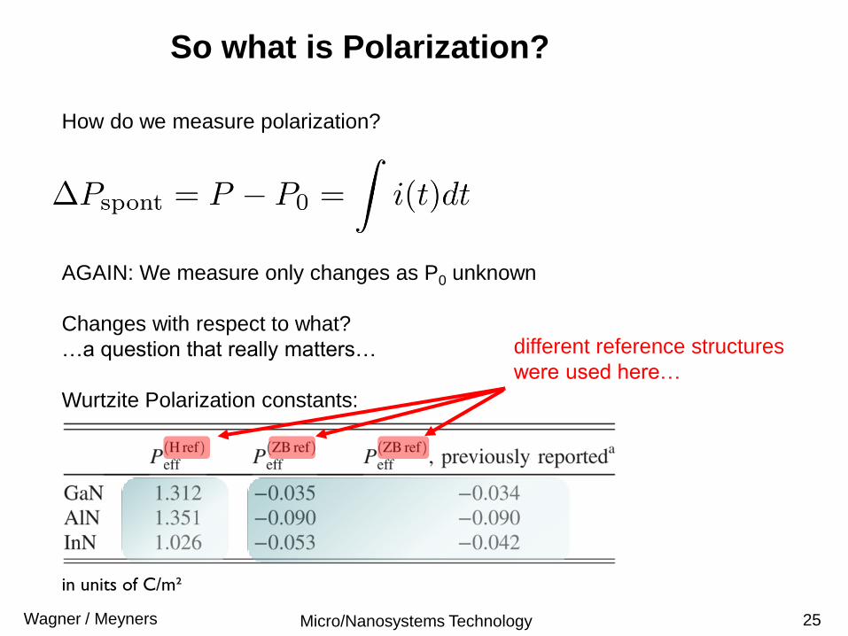
So what is Polarization?
How do we measure polarization?
AGAIN: We measure only changes as P0 unknown
Changes with respect to what?
…a question that really matters…
Wurtzite Polarization constants:
in units of C/m²
different reference structures
were used here…
Micro/Nanosystems TechnologyWagner / Meyners 26
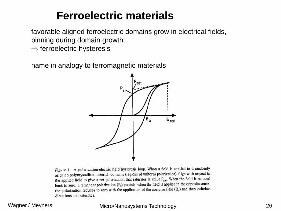
favorable aligned ferroelectric domains grow in electrical fields,
pinning during domain growth:
ferroelectric hysteresis
name in analogy to ferromagnetic materials
Ferroelectric materialsFerroelectric materials
Micro/Nanosystems TechnologyWagner / Meyners 27
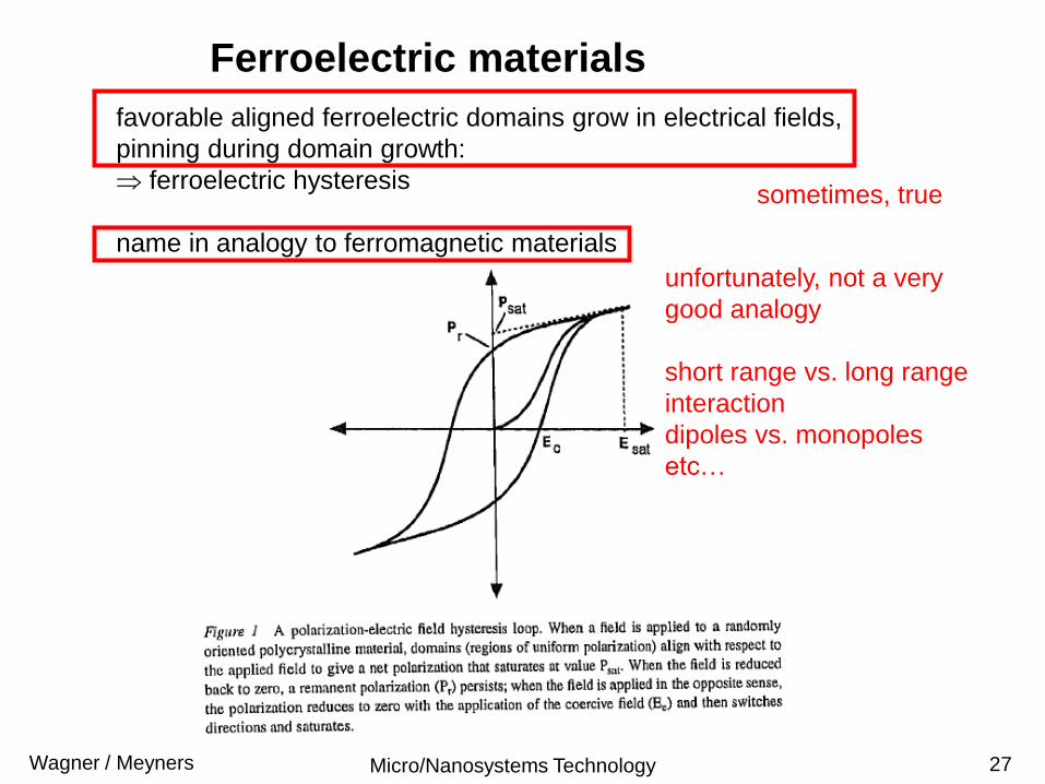
favorable aligned ferroelectric domains grow in electrical fields,
pinning during domain growth:
ferroelectric hysteresis
name in analogy to ferromagnetic materials
Ferroelectric materialsFerroelectric materials
sometimes, true
unfortunately, not a very
good analogy
short range vs. long range
interaction
dipoles vs. monopoles
etc…
Micro/Nanosystems TechnologyWagner / Meyners 28
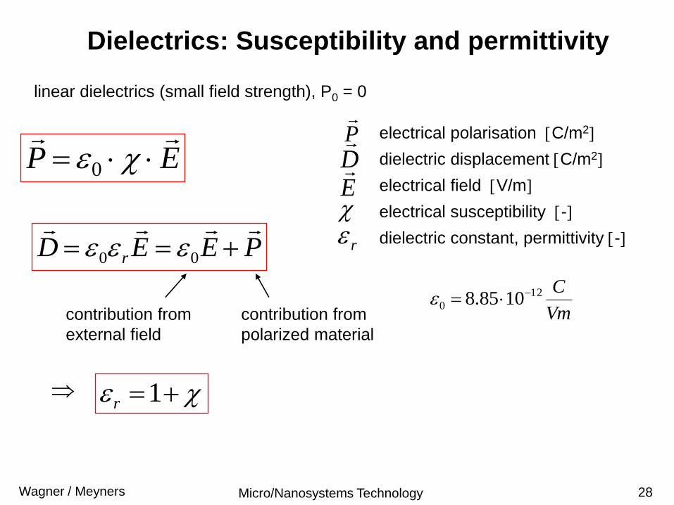
EP
0
electrical polarisation C/m2
dielectric displacement C/m2
electrical field V/m
electrical susceptibility -
dielectric constant, permittivity -
linear dielectrics (small field strength), P0 = 0
PEED r
00
D
1r
E
contribution from
external field
contribution from
polarized material
P
Vm
C12
0 1085.8
r
Dielectrics: Susceptibility and permittivity
Micro/Nanosystems TechnologyWagner / Meyners 29
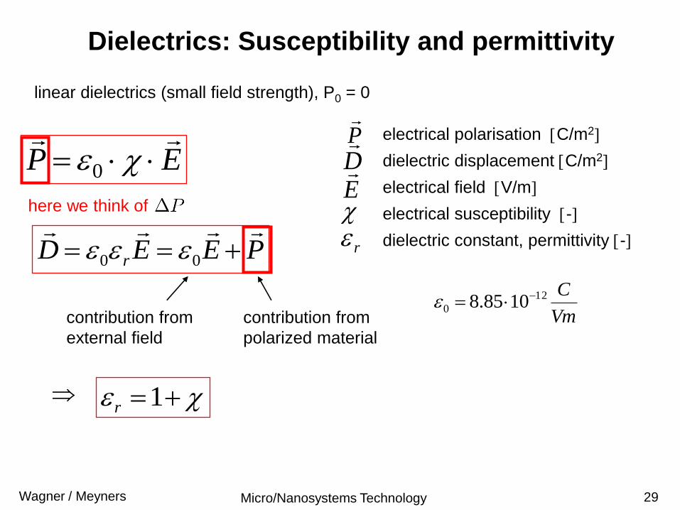
EP
0
electrical polarisation C/m2
dielectric displacement C/m2
electrical field V/m
electrical susceptibility -
dielectric constant, permittivity -
linear dielectrics (small field strength), P0 = 0
PEED r
00
D
1r
E
contribution from
external field
contribution from
polarized material
P
Vm
C12
0 1085.8
r
Dielectrics: Susceptibility and permittivity
here we think of
Micro/Nanosystems TechnologyWagner / Meyners 30
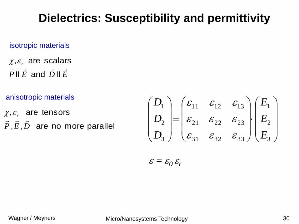
isotropic materials
EDEP
r
II and II
scalars are ,
anisotropic materials
parallel more no are , ,
tensors are
DEP
r
,
3
2
1
333231
232221
131211
3
2
1
E
E
E
D
D
D
= 0 r
Dielectrics: Susceptibility and permittivity
Micro/Nanosystems TechnologyWagner / Meyners 31
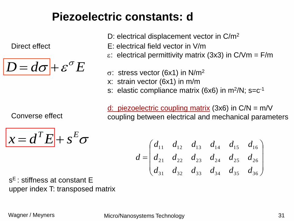
Piezoelectric constants: d
EdD
ET sEdx
D: electrical displacement vector in C/m2
E: electrical field vector in V/m
: electrical permittivity matrix (3x3) in C/Vm = F/m
: stress vector (6x1) in N/m2
x: strain vector (6x1) in m/m
s: elastic compliance matrix (6x6) in m2/N; s=c-1
d: piezoelectric coupling matrix (3x6) in C/N = m/V
coupling between electrical and mechanical parameters
Direct effect
Converse effect
sE : stiffness at constant E
upper index T: transposed matrix
363534333231
262524232221
161514131211
dddddd
dddddd
dddddd
d
Micro/Nanosystems TechnologyWagner / Meyners 32
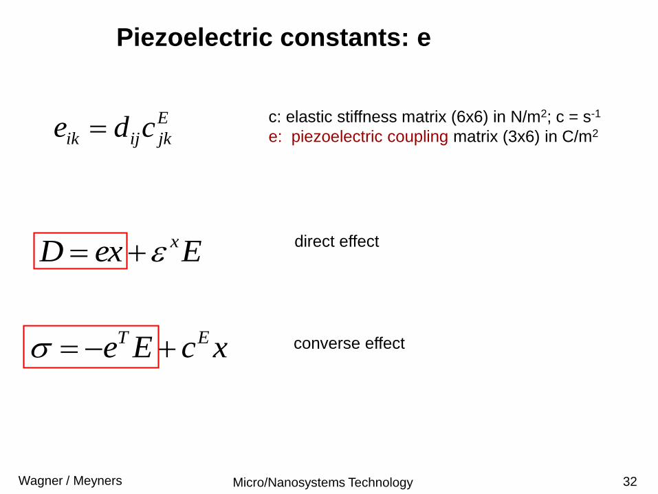
EexD x
xcEe ET converse effect
E
jkijik cde
direct effect
c: elastic stiffness matrix (6x6) in N/m2; c = s-1
e: piezoelectric coupling matrix (3x6) in C/m2
Piezoelectric constants: e
Micro/Nanosystems TechnologyWagner / Meyners 33
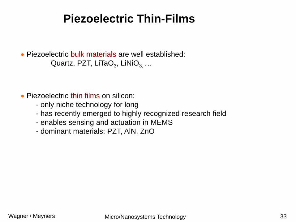
Piezoelectric Thin-Films
Piezoelectric bulk materials are well established:
Quartz, PZT, LiTaO3, LiNiO3, …
Piezoelectric thin films on silicon:
- only niche technology for long
- has recently emerged to highly recognized research field
- enables sensing and actuation in MEMS
- dominant materials: PZT, AlN, ZnO
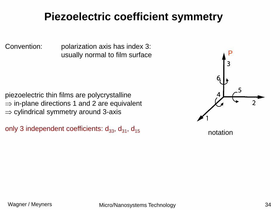
Micro/Nanosystems TechnologyWagner / Meyners 34
piezoelectric thin films are polycrystalline
in-plane directions 1 and 2 are equivalent
cylindrical symmetry around 3-axis
only 3 independent coefficients: d33, d31, d15
Convention: polarization axis has index 3:
usually normal to film surface
notation
P
Piezoelectric coefficient symmetryPiezoelectric coefficient symmetry
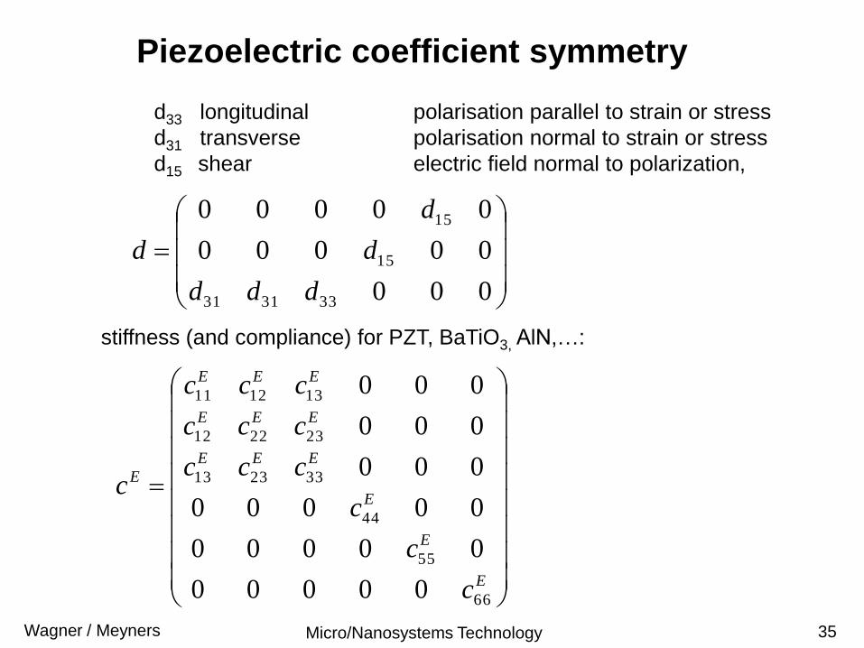
Micro/Nanosystems TechnologyWagner / Meyners 35
000
00000
00000
333131
15
15
ddd
d
d
d
d33 longitudinal polarisation parallel to strain or stress
d31 transverse polarisation normal to strain or stress
d15 shear electric field normal to polarization,
Piezoelectric coefficient symmetry
stiffness (and compliance) for PZT, BaTiO3, AlN,…:
E
E
E
EEE
EEE
EEE
E
c
c
c
ccc
ccc
ccc
c
66
55
44
332313
232212
131211
00000
00000
00000
000
000
000
Micro/Nanosystems TechnologyWagner / Meyners 36
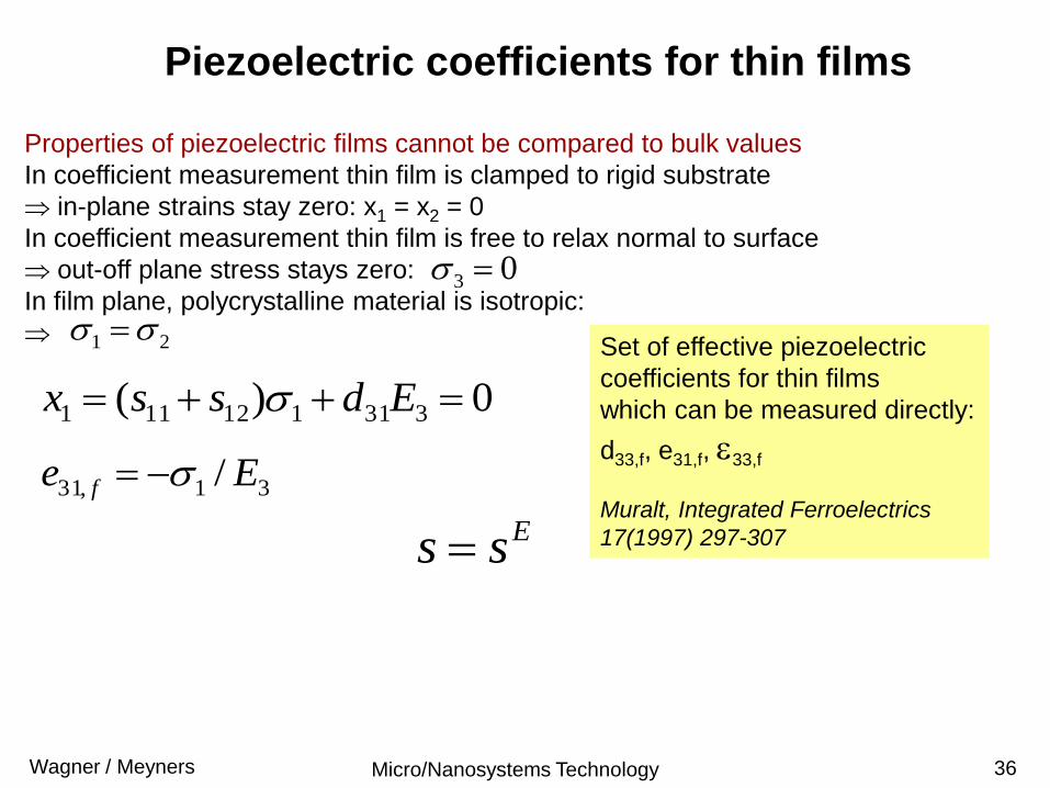
Piezoelectric coefficients for thin films
Properties of piezoelectric films cannot be compared to bulk values
In coefficient measurement thin film is clamped to rigid substrate
in-plane strains stay zero: x1 = x2 = 0
In coefficient measurement thin film is free to relax normal to surface
out-off plane stress stays zero:
In film plane, polycrystalline material is isotropic:
0)( 331112111 Edssx
31,31 / Ee f
Set of effective piezoelectric
coefficients for thin films
which can be measured directly:
d33,f, e31,f, 33,f
Muralt, Integrated Ferroelectrics
17(1997) 297-307Ess
03
21
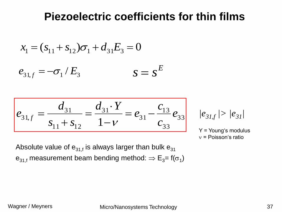
Micro/Nanosystems TechnologyWagner / Meyners 37
Absolute value of e31,f is always larger than bulk e31
e31,f measurement beam bending method: E3= f(1)
Y = Young‘s modulus
= Poisson‘s ratio
0)( 331112111 Edssx
31,31 / Ee f Ess
Piezoelectric coefficients for thin films
33
33
1331
31
1211
31,31
1e
c
ce
Yd
ss
de f
|e31,f |> |e31|
Micro/Nanosystems TechnologyWagner / Meyners 38
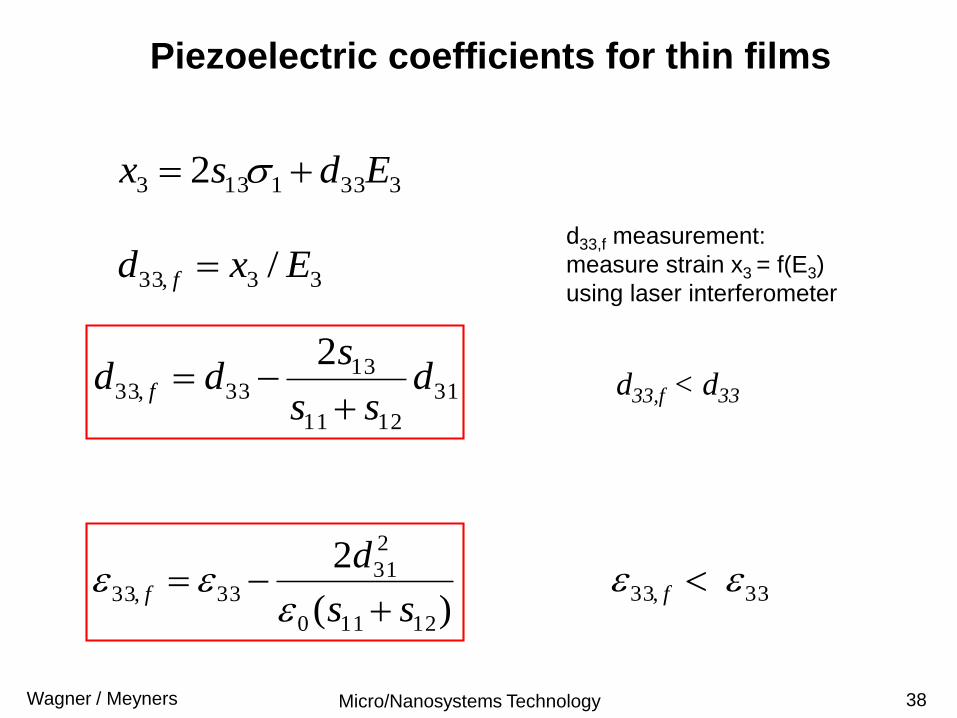
3331133 2 Edsx
33,33 / Exd f
d33,f < d3331
1211
1333,33
2d
ss
sdd f
d33,f measurement:
measure strain x3 = f(E3)
using laser interferometer
)(
2
12110
2
3133,33
ss
df
33,33 f
Piezoelectric coefficients for thin films
Micro/Nanosystems TechnologyWagner / Meyners 39
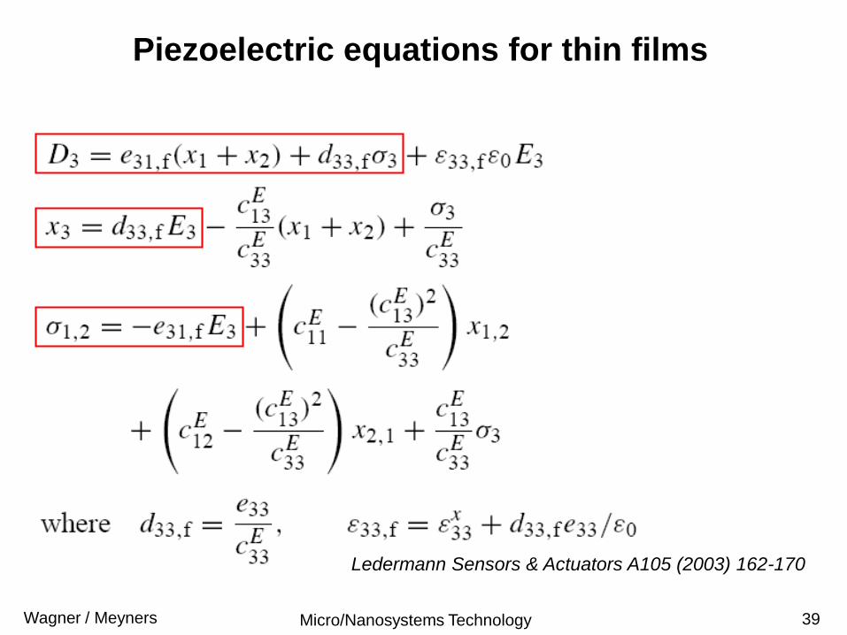
Ledermann Sensors & Actuators A105 (2003) 162-170
Piezoelectric equations for thin films
Micro/Nanosystems TechnologyWagner / Meyners 40
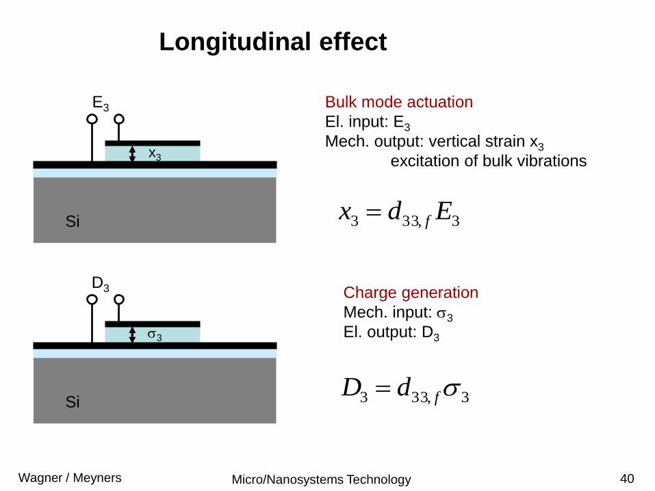
Longitudinal effect
3,333 fdD
Bulk mode actuation
El. input: E3
Mech. output: vertical strain x3
excitation of bulk vibrations
E3
Si
x3
D3
Si
3
Charge generation
Mech. input: 3
El. output: D3
3,333 Edx f
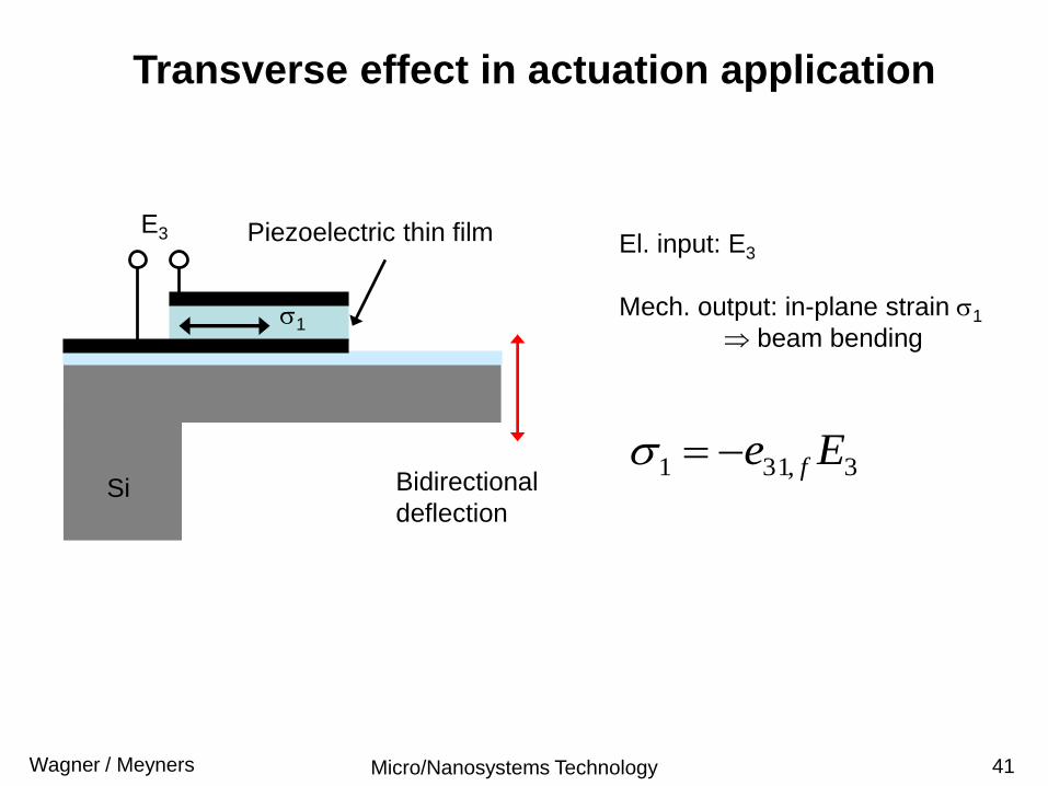
Micro/Nanosystems TechnologyWagner / Meyners 41
El. input: E3
Mech. output: in-plane strain 1
beam bending
3,311 Ee f
Transverse effect in actuation application
Piezoelectric thin filmE3
Si
1
Bidirectional
deflection
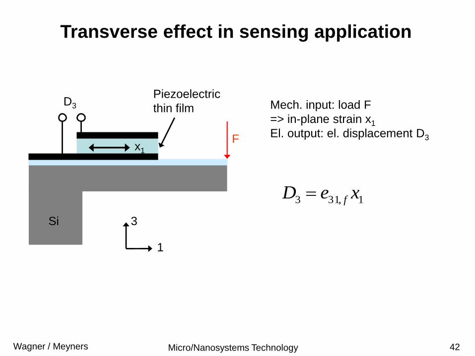
Micro/Nanosystems TechnologyWagner / Meyners 42
Transverse effect in sensing application
Mech. input: load F
=> in-plane strain x1
El. output: el. displacement D3
1,313 xeD f
1
F
Piezoelectric
thin film
x1
D3
Si 3
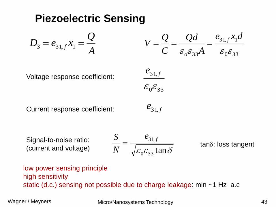
Micro/Nanosystems TechnologyWagner / Meyners 43
330
1,31
33
dxe
A
Qd
C
QV
f
o
A
QxeD f 1,313
Voltage response coefficient:
330
,31
fe
Signal-to-noise ratio:
(current and voltage) tan330
,31 fe
N
S
low power sensing principle
high sensitivity
static (d.c.) sensing not possible due to charge leakage: min ~1 Hz a.c
tan: loss tangent
Piezoelectric Sensing
Current response coefficient: fe ,31
Micro/Nanosystems TechnologyWagner / Meyners 44
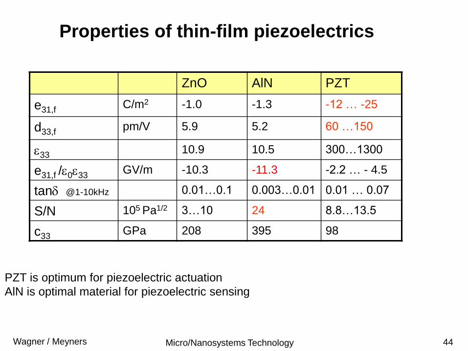
Properties of thinfilm piezoelectrics
ZnO AlN PZT
e31,fC/m2 -1.0 -1.3 -12 … -25
d33,fpm/V 5.9 5.2 60 …150
3310.9 10.5 300…1300
e31,f /033GV/m -10.3 -11.3 -2.2 … - 4.5
tan @1-10kHz 0.01…0.1 0.003…0.01 0.01 … 0.07
S/N 105 Pa1/2 3…10 24 8.8…13.5
c33GPa 208 395 98
PZT is optimum for piezoelectric actuation
AlN is optimal material for piezoelectric sensing
Properties of thin-film piezoelectrics
Micro/Nanosystems TechnologyWagner / Meyners 45
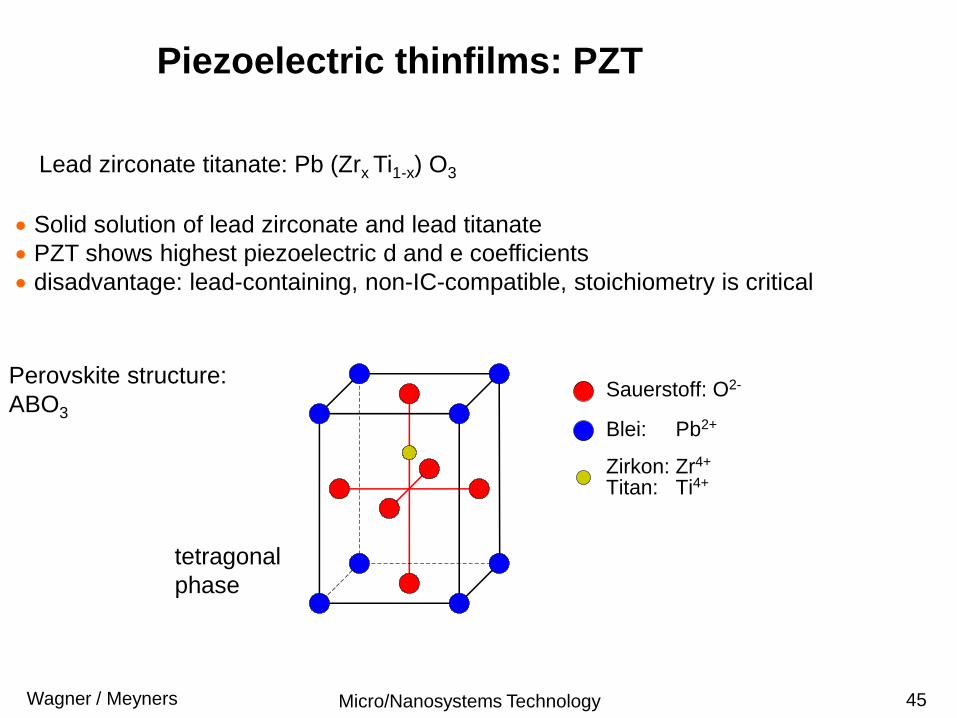
Piezoelectric thinfilms: PZT
Solid solution of lead zirconate and lead titanate
PZT shows highest piezoelectric d and e coefficients
disadvantage: lead-containing, non-IC-compatible, stoichiometry is critical
Lead zirconate titanate: Pb (Zrx Ti1-x) O3
Sauerstoff: O2-
Blei: Pb2+
Zirkon: Zr4+
Titan: Ti4+
tetragonal
phase
Perovskite structure:
ABO3
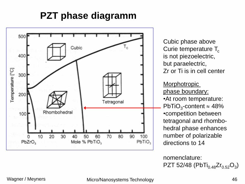
Micro/Nanosystems TechnologyWagner / Meyners 46
Cubic phase above
Curie temperature Tc
is not piezoelectric,
but paraelectric,
Zr or Ti is in cell center
Morphotropic
phase boundary:
•At room temperature:
PbTiO3-content 48%
•competition between
tetragonal and rhombo-
hedral phase enhances
number of polarizable
directions to 14
nomenclature:
PZT 52/48 (PbTi0.48Zr0.52O3)
PZT phase diagramm
Micro/Nanosystems TechnologyWagner / Meyners 47
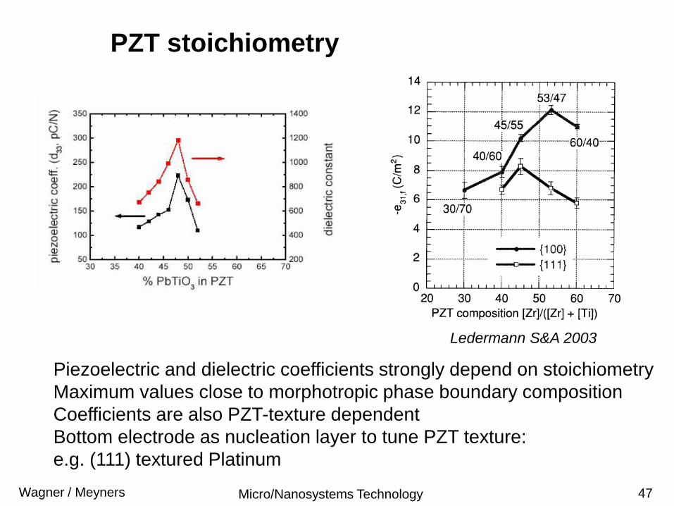
Piezoelectric and dielectric coefficients strongly depend on stoichiometry
Maximum values close to morphotropic phase boundary composition
Coefficients are also PZT-texture dependent
Bottom electrode as nucleation layer to tune PZT texture:
e.g. (111) textured Platinum
Ledermann S&A 2003
PZT stoichiometry
Micro/Nanosystems TechnologyWagner / Meyners 48
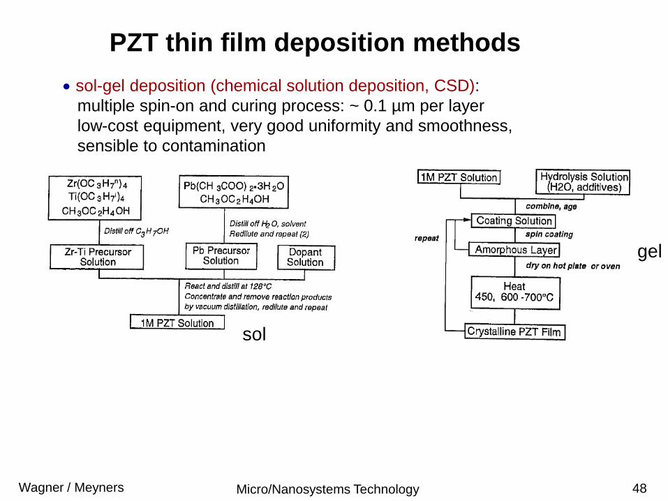
sol-gel deposition (chemical solution deposition, CSD):
multiple spin-on and curing process: ~ 0.1 µm per layer
low-cost equipment, very good uniformity and smoothness,
sensible to contamination
sol
gel
PZT thin film deposition methods
Micro/Nanosystems TechnologyWagner / Meyners 49
PZT thin film deposition methods
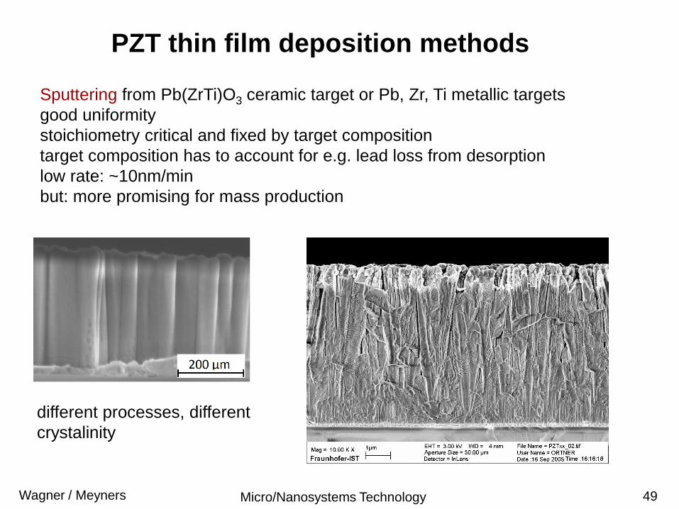
Sputtering from Pb(ZrTi)O3 ceramic target or Pb, Zr, Ti metallic targets
good uniformity
stoichiometry critical and fixed by target composition
target composition has to account for e.g. lead loss from desorption
low rate: ~10nm/min
but: more promising for mass production
different processes, different
crystalinity
Micro/Nanosystems TechnologyWagner / Meyners 50
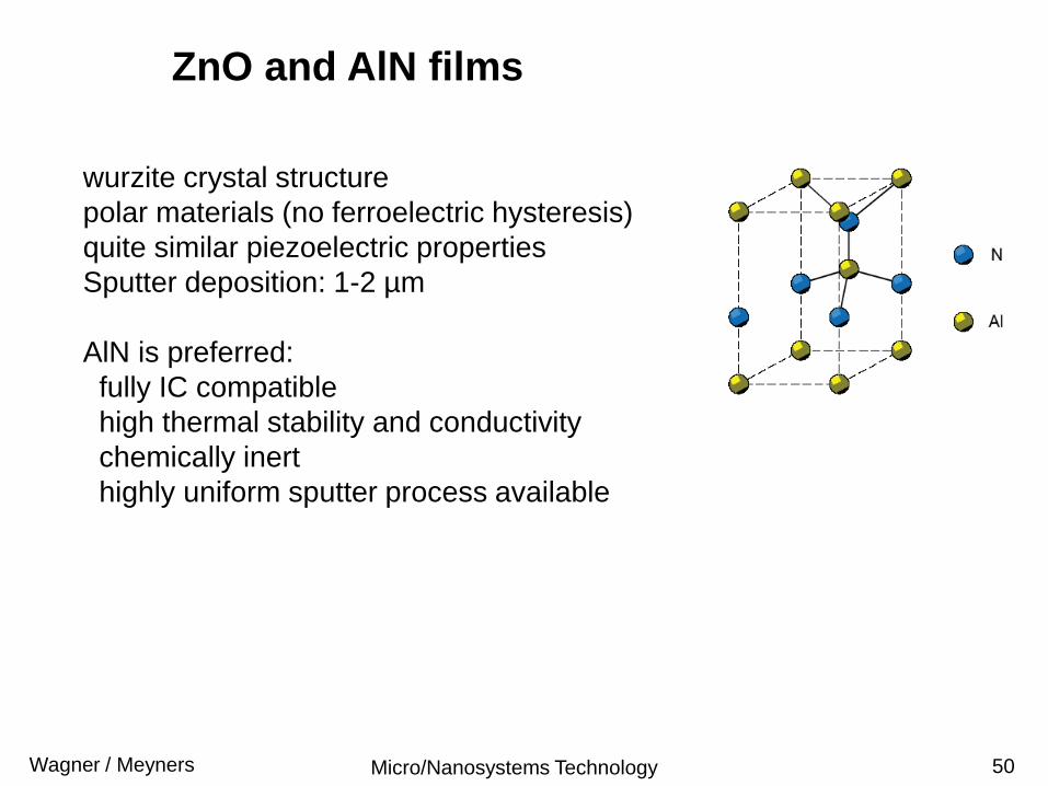
wurzite crystal structure
polar materials (no ferroelectric hysteresis)
quite similar piezoelectric properties
Sputter deposition: 1-2 µm
AlN is preferred:
fully IC compatible
high thermal stability and conductivity
chemically inert
highly uniform sputter process available
ZnO and AlN films
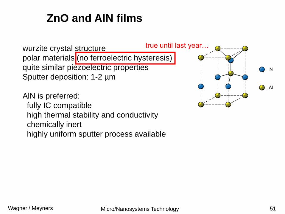
Micro/Nanosystems TechnologyWagner / Meyners 51
wurzite crystal structure
polar materials (no ferroelectric hysteresis)
quite similar piezoelectric properties
Sputter deposition: 1-2 µm
AlN is preferred:
fully IC compatible
high thermal stability and conductivity
chemically inert
highly uniform sputter process available
ZnO and AlN films
true until last year…
Micro/Nanosystems TechnologyWagner / Meyners 52
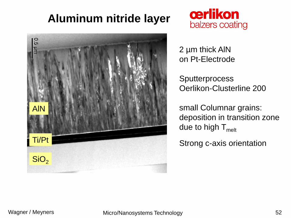
2 µm thick AlN
on Pt-Electrode
Sputterprocess
Oerlikon-Clusterline 200
small Columnar grains:
deposition in transition zone
due to high Tmelt
Strong c-axis orientation Ti/Pt
SiO2
AlN
Aluminum nitride layer
Micro/Nanosystems TechnologyWagner / Meyners 53
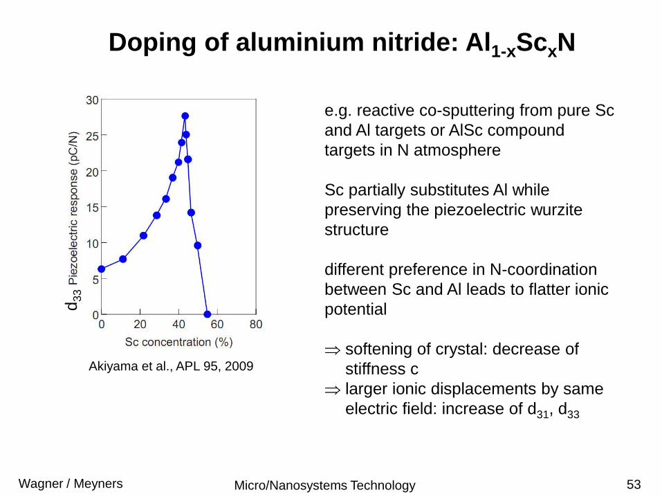
Doping of aluminium nitride: Al1-xScxN
Akiyama et al., APL 95, 2009
e.g. reactive co-sputtering from pure Sc
and Al targets or AlSc compound
targets in N atmosphere
Sc partially substitutes Al while
preserving the piezoelectric wurzite
structure
different preference in N-coordination
between Sc and Al leads to flatter ionic
potential
softening of crystal: decrease of
stiffness c
larger ionic displacements by same
electric field: increase of d31, d33
d3
3
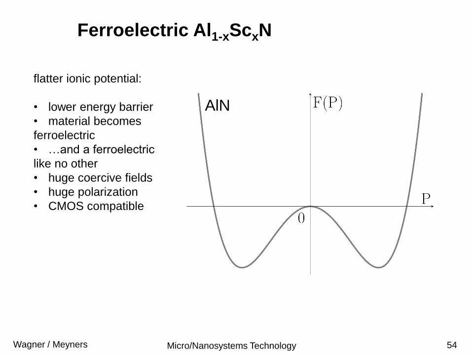
Micro/Nanosystems TechnologyWagner / Meyners 54
Ferroelectric Al1-xScxN
AlN
flatter ionic potential:
• lower energy barrier
• material becomes
ferroelectric
• …and a ferroelectric
like no other
• huge coercive fields
• huge polarization
• CMOS compatible
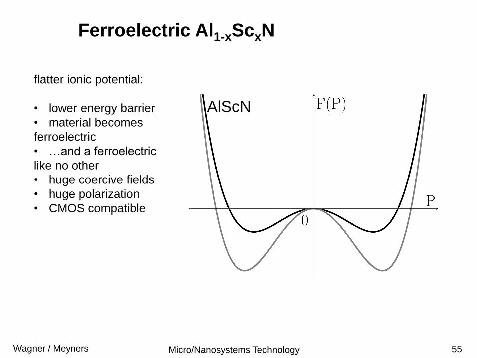
Micro/Nanosystems TechnologyWagner / Meyners 55
Ferroelectric Al1-xScxN
AlScN
flatter ionic potential:
• lower energy barrier
• material becomes
ferroelectric
• …and a ferroelectric
like no other
• huge coercive fields
• huge polarization
• CMOS compatible
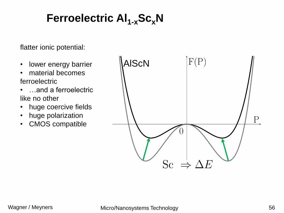
Micro/Nanosystems TechnologyWagner / Meyners 56
Ferroelectric Al1-xScxN
AlScN
flatter ionic potential:
• lower energy barrier
• material becomes
ferroelectric
• …and a ferroelectric
like no other
• huge coercive fields
• huge polarization
• CMOS compatible
Micro/Nanosystems TechnologyWagner / Meyners 57
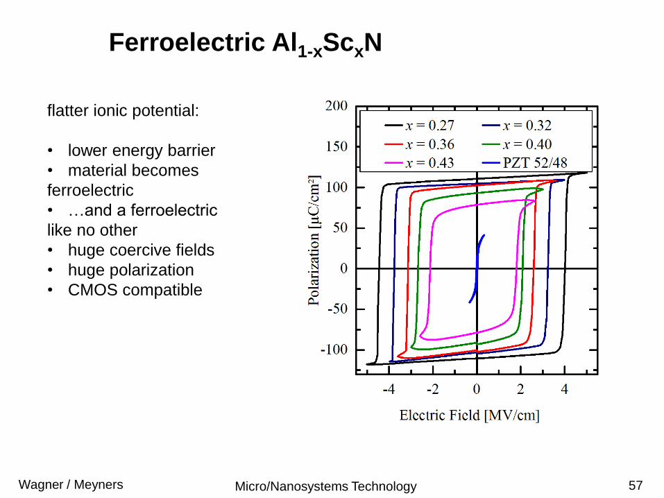
Ferroelectric Al1-xScxN
flatter ionic potential:
• lower energy barrier
• material becomes
ferroelectric
• …and a ferroelectric
like no other
• huge coercive fields
• huge polarization
• CMOS compatible
Micro/Nanosystems TechnologyWagner / Meyners 58
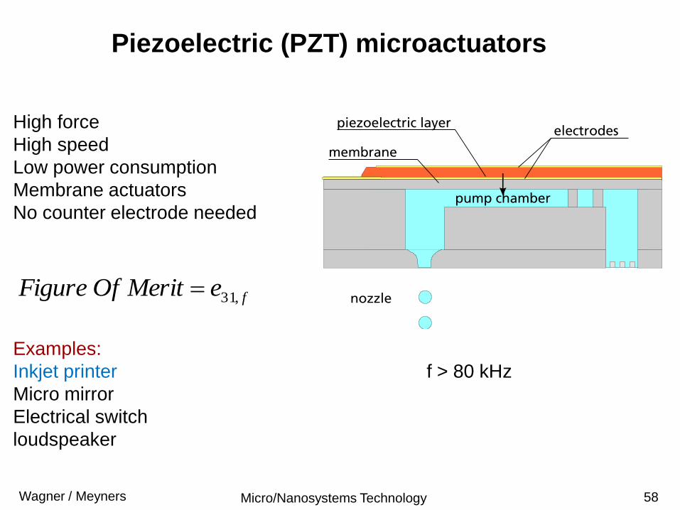
High force
High speed
Low power consumption
Membrane actuators
No counter electrode needed
Examples:
Inkjet printer f > 80 kHz
Micro mirror
Electrical switch
loudspeaker
membrane
piezoelectric layerelectrodes
nozzle
pump chamber
Piezoelectric (PZT) microactuators
feMeritOfFigure ,31
Micro/Nanosystems TechnologyWagner / Meyners 59
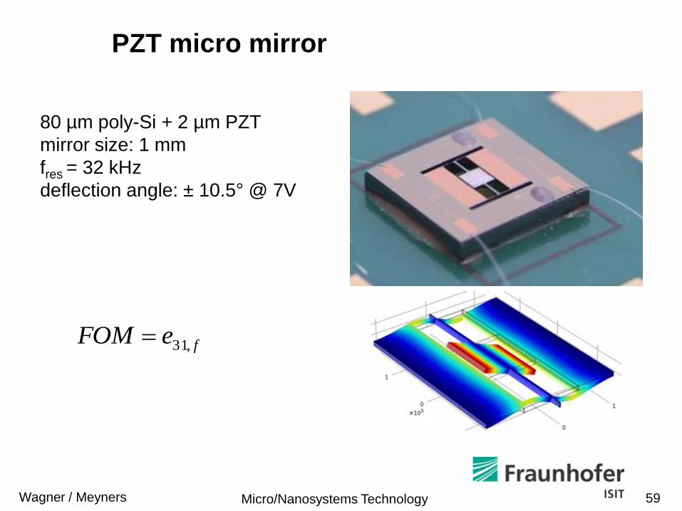
PZT micro mirror
80 µm poly-Si + 2 µm PZT
mirror size: 1 mm
fres = 32 kHz
deflection angle: ± 10.5° @ 7V
feFOM ,31
Micro/Nanosystems TechnologyWagner / Meyners 60
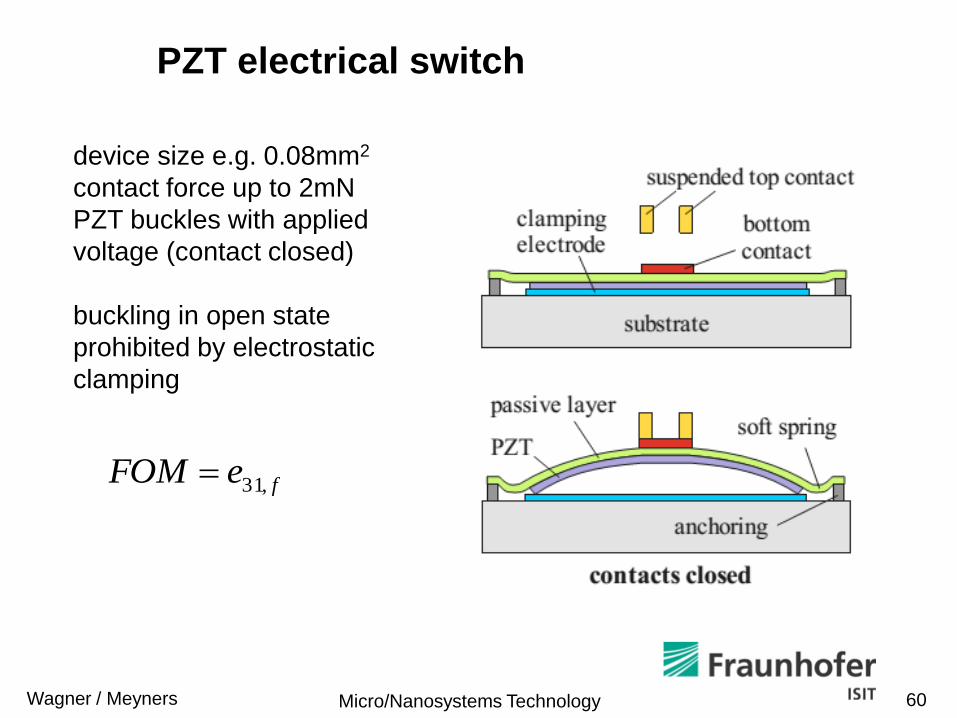
PZT electrical switch
device size e.g. 0.08mm2
contact force up to 2mN
PZT buckles with applied
voltage (contact closed)
buckling in open state
prohibited by electrostatic
clamping
feFOM ,31
Micro/Nanosystems TechnologyWagner / Meyners 61
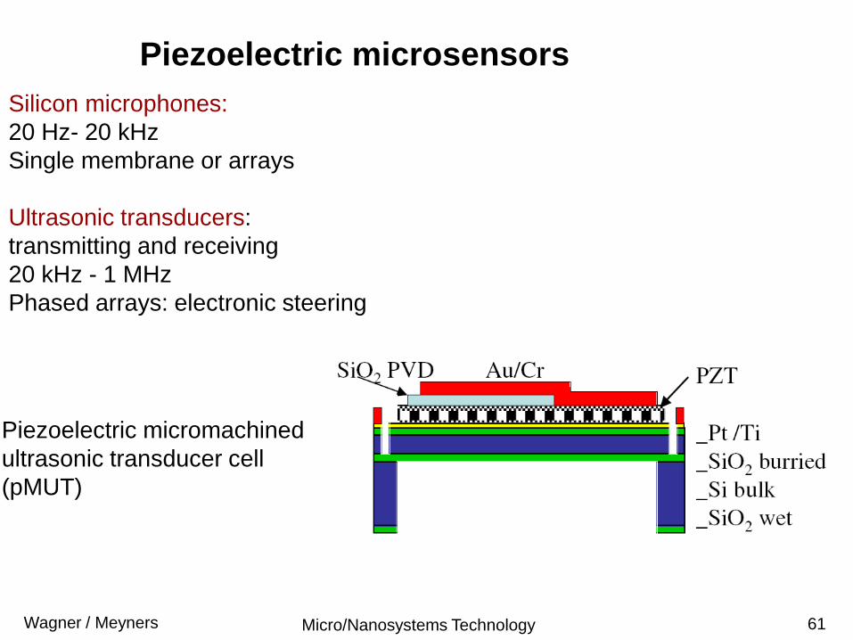
Silicon microphones:
20 Hz- 20 kHz
Single membrane or arrays
Ultrasonic transducers:
transmitting and receiving
20 kHz - 1 MHz
Phased arrays: electronic steering
Piezoelectric micromachined
ultrasonic transducer cell
(pMUT)
Piezoelectric microsensors
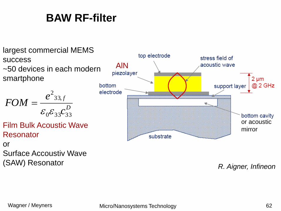
Micro/Nanosystems TechnologyWagner / Meyners 62
R. Aigner, Infineon
AlN
largest commercial MEMS
success
~50 devices in each modern
smartphone
Film Bulk Acoustic Wave
Resonator
or
Surface Accoustiv Wave
(SAW) Resonator
BAW RF-filter
D
f
c
eFOM
33330
,332
or acoustic
mirror
PadsPZT
Elektrode
Micro/Nanosystems TechnologyWagner / Meyners 63
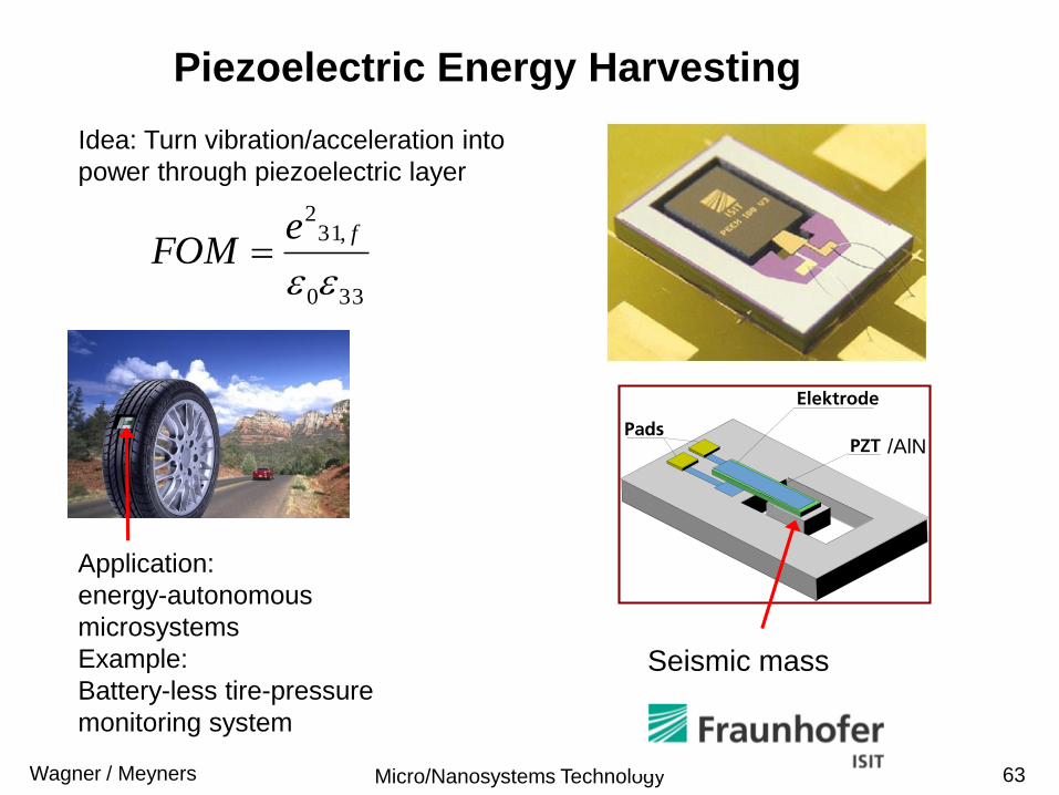
Piezoelectric Energy Harvesting
Idea: Turn vibration/acceleration into
power through piezoelectric layer
Seismic mass
/AlN
Application:
energy-autonomous
microsystems
Example:
Battery-less tire-pressure
monitoring system
330
,312
feFOM
Micro/Nanosystems TechnologyWagner / Meyners 64
Summary
only changes in polarization matter
piezoelectric coupling matrices: d and e
effective piezoelectric coefficents for thin films: d33,f, e31,f
dominant thinfilm materials: PZT, AlN, AlScN
PZT optimum for microactuation
AlN optimum for sensing
AlScN can combine advantages of both AlN and PZT
broad range of piezoelectric MEMS applications
Micro/Nanosystems TechnologyWagner / Meyners 65
Literature
Madou pp. 551-560
Chang Liu Foundations of MEMS CH. 7
N. Setter Electroceramic-based MEMS, 2005
esp. Ch. 10 Thin film piezoelectrics for MEMS
by S. Trolier-McKinstry and P. Muralt