Embed Size (px)
Citation preview

Microprocessor Laboratory
Part 1: 8051
Viking Tang & Marvin Lee
Department of
Biomedical Engineering Yuanpei University
2008/09/01
Viking & Marvin, μPLab9701 BME.YPU
I
Table of Content Table of Content................................................................................................................................... I
LAB 00: Introduction to 8051............................................................................................................. 1
LAB 01: Port I/O by μVision.............................................................................................................. 2
LAB 02: Port I/O by ICE .................................................................................................................... 3
LAB 03: Port I/O by AT89S51........................................................................................................... 4
LAB 04: P2 Chasing ........................................................................................................................... 5
LAB 05: Arithmetic Operations.......................................................................................................... 7
LAB 06: Look-up Table...................................................................................................................... 9
LAB 07: Timer Programming........................................................................................................... 11
LAB 08: Serial Interfacing................................................................................................................ 13
LAB 09: Interrupt Programming....................................................................................................... 15
LAB 10: ADC0804 Testing .............................................................................................................. 17
LAB 11: ADC Programming ............................................................................................................ 19
LAB 12: ADC and Serial Interfacing ............................................................................................... 21
Appendix........................................................................................................................................... 22
A.1. Schedule:....................................................................................................................... 23
A.2. Elements & Tools.......................................................................................................... 24
A.3. Lab Report..................................................................................................................... 27
A.4. PC Applications............................................................................................................. 30
A.5. OrCAD/Capture Tutorial............................................................................................... 36
A.6. Keil μVision C51 Tutorial............................................................................................. 44
A.7. K&H ICE Tutorial......................................................................................................... 56
A.8. AT89S51 ISP Tutorial ................................................................................................... 61
A.9. Super Terminal Tutorial ................................................................................................ 66
A.10. ASCII ............................................................................................................................ 68
A.11. C Data Types and Operators ......................................................................................... 70

Viking & Marvin, μPLab9701 BME.YPU
1
LAB 00: Introduction to 8051 8051 CONCEPT:
Viking & Marvin, μPLab9701 BME.YPU
2
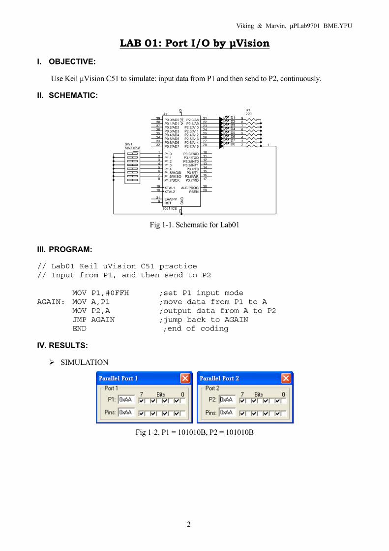
LAB 01: Port I/O by μVision I. OBJECTIVE:
Use Keil μVision C51 to simulate: input data from P1 and then send to P2, continuously.
II. SCHEMATIC:
Fig 1-1. Schematic for Lab01
III. PROGRAM:
// Lab01 Keil uVision C51 practice // Input from P1, and then send to P2 MOV P1,#0FFH ;set P1 input mode AGAIN: MOV A,P1 ;move data from P1 to A MOV P2,A ;output data from A to P2 JMP AGAIN ;jump back to AGAIN END ;end of coding
IV. RESULTS:
SIMULATION
Fig 1-2. P1 = 101010B, P2 = 101010B
Viking & Marvin, μPLab9701 BME.YPU
3
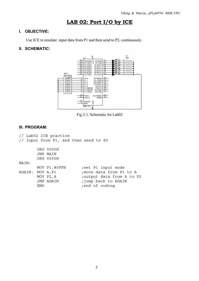
LAB 02: Port I/O by ICE I. OBJECTIVE:
Use ICE to emulate: input data from P1 and then send to P2, continuously.
II. SCHEMATIC:
Fig 2-1. Schematic for Lab02
III. PROGRAM:
// Lab02 ICE practice // Input from P1, and then send to P2 ORG 0000H JMP MAIN ORG 0050H MAIN: MOV P1,#0FFH ;set P1 input mode AGAIN: MOV A,P1 ;move data from P1 to A MOV P2,A ;output data from A to P2 JMP AGAIN ;jump back to AGAIN END ;end of coding
Viking & Marvin, μPLab9701 BME.YPU
4
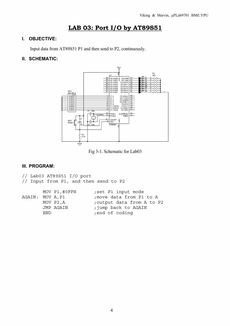
LAB 03: Port I/O by AT89S51 I. OBJECTIVE:
Input data from AT89S51 P1 and then send to P2, continuously.
II. SCHEMATIC:
Fig 3-1. Schematic for Lab03
III. PROGRAM:
// Lab03 AT89S51 I/O port // Input from P1, and then send to P2 MOV P1,#0FFH ;set P1 input mode AGAIN: MOV A,P1 ;move data from P1 to A MOV P2,A ;output data from A to P2 JMP AGAIN ;jump back to AGAIN END ;end of coding
Viking & Marvin, μPLab9701 BME.YPU
5
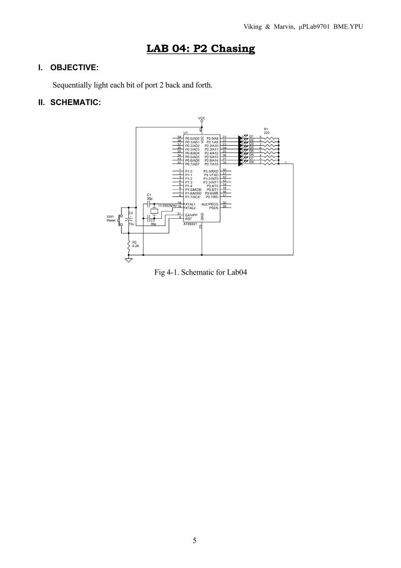
LAB 04: P2 Chasing I. OBJECTIVE:
Sequentially light each bit of port 2 back and forth.
II. SCHEMATIC:
Fig 4-1. Schematic for Lab04
Viking & Marvin, μPLab9701 BME.YPU
6
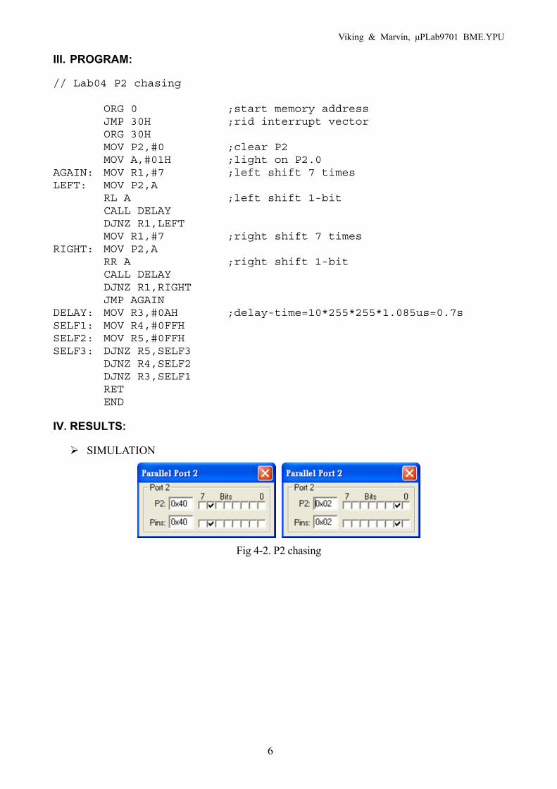
III. PROGRAM:
// Lab04 P2 chasing ORG 0 ;start memory address JMP 30H ;rid interrupt vector ORG 30H MOV P2,#0 ;clear P2 MOV A,#01H ;light on P2.0 AGAIN: MOV R1,#7 ;left shift 7 times LEFT: MOV P2,A RL A ;left shift 1-bit CALL DELAY DJNZ R1,LEFT MOV R1,#7 ;right shift 7 times RIGHT: MOV P2,A RR A ;right shift 1-bit CALL DELAY DJNZ R1,RIGHT JMP AGAIN DELAY: MOV R3,#0AH ;delay-time=10*255*255*1.085us=0.7s SELF1: MOV R4,#0FFH SELF2: MOV R5,#0FFH SELF3: DJNZ R5,SELF3 DJNZ R4,SELF2 DJNZ R3,SELF1 RET END
IV. RESULTS:
SIMULATION
Fig 4-2. P2 chasing
Viking & Marvin, μPLab9701 BME.YPU
7
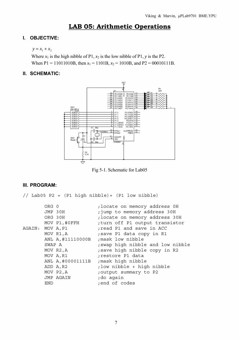
LAB 05: Arithmetic Operations I. OBJECTIVE:
21 xxy += Where x1 is the high nibble of P1, x2 is the low nibble of P1, y is the P2. When P1 = 11011010B, then x1 = 1101B, x2 = 1010B, and P2 = 00010111B.
II. SCHEMATIC:
Fig 5-1. Schematic for Lab05
III. PROGRAM:
// Lab05 P2 = (P1 high nibble)+ (P1 low nibble) ORG 0 ;locate on memory address 0H JMP 30H ;jump to memory address 30H ORG 30H ;locate on memory address 30H MOV P1,#0FFH ;turn off P1 output transistor AGAIN: MOV A,P1 ;read P1 and save in ACC MOV R1,A ;save P1 data copy in R1 ANL A,#11110000B ;mask low nibble SWAP A ;swap high nibble and low nibble MOV R2,A ;save high nibble copy in R2 MOV A,R1 ;restore P1 data ANL A,#00001111B ;mask high nibble ADD A,R2 ;low nibble + high nibble MOV P2,A ;output summary to P2 JMP AGAIN ;do again END ;end of codes

Viking & Marvin, μPLab9701 BME.YPU
8
IV. RESULTS:
SIMULATION
Fig 5-2. P1 = 11011010B, and P2 = 1101B + 1010B = 00010111B
Viking & Marvin, μPLab9701 BME.YPU
9
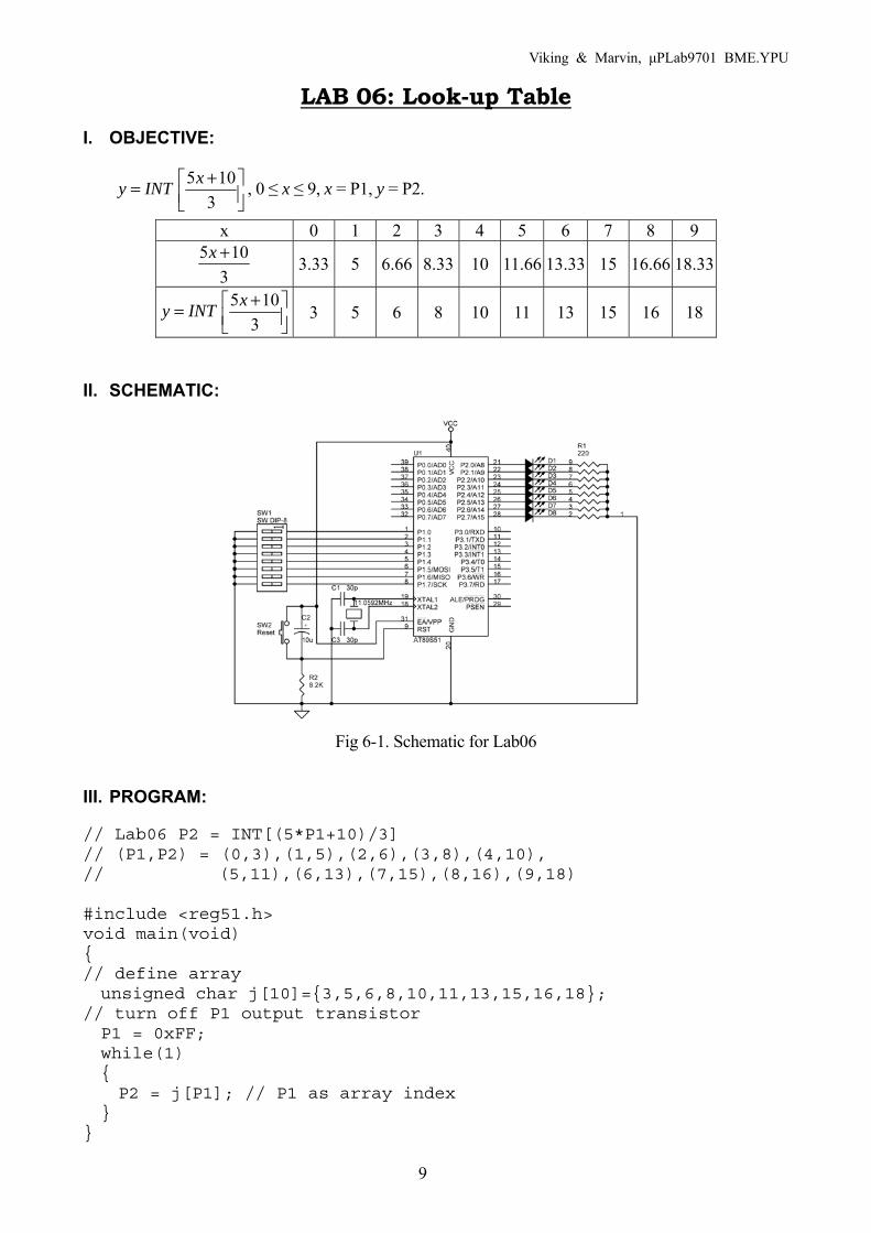
LAB 06: Look-up Table I. OBJECTIVE:
⎥⎦⎤
⎢⎣⎡ +=
3105xINTy , 0 ≤ x ≤ 9, x = P1, y = P2.
x 0 1 2 3 4 5 6 7 8 9
3105 +x 3.33 5 6.66 8.33 10 11.66 13.33 15 16.66 18.33
⎥⎦⎤
⎢⎣⎡ +=
3105xINTy 3 5 6 8 10 11 13 15 16 18
II. SCHEMATIC:
Fig 6-1. Schematic for Lab06
III. PROGRAM:
// Lab06 P2 = INT[(5*P1+10)/3] // (P1,P2) = (0,3),(1,5),(2,6),(3,8),(4,10), // (5,11),(6,13),(7,15),(8,16),(9,18) #include <reg51.h> void main(void) // define array unsigned char j[10]=3,5,6,8,10,11,13,15,16,18; // turn off P1 output transistor P1 = 0xFF; while(1) P2 = j[P1]; // P1 as array index

Viking & Marvin, μPLab9701 BME.YPU
10
IV. RESULTS:
SIMULATION
Fig 6-2. P1 = 0x09, and P2 = 0x12 = 18
Viking & Marvin, μPLab9701 BME.YPU
11
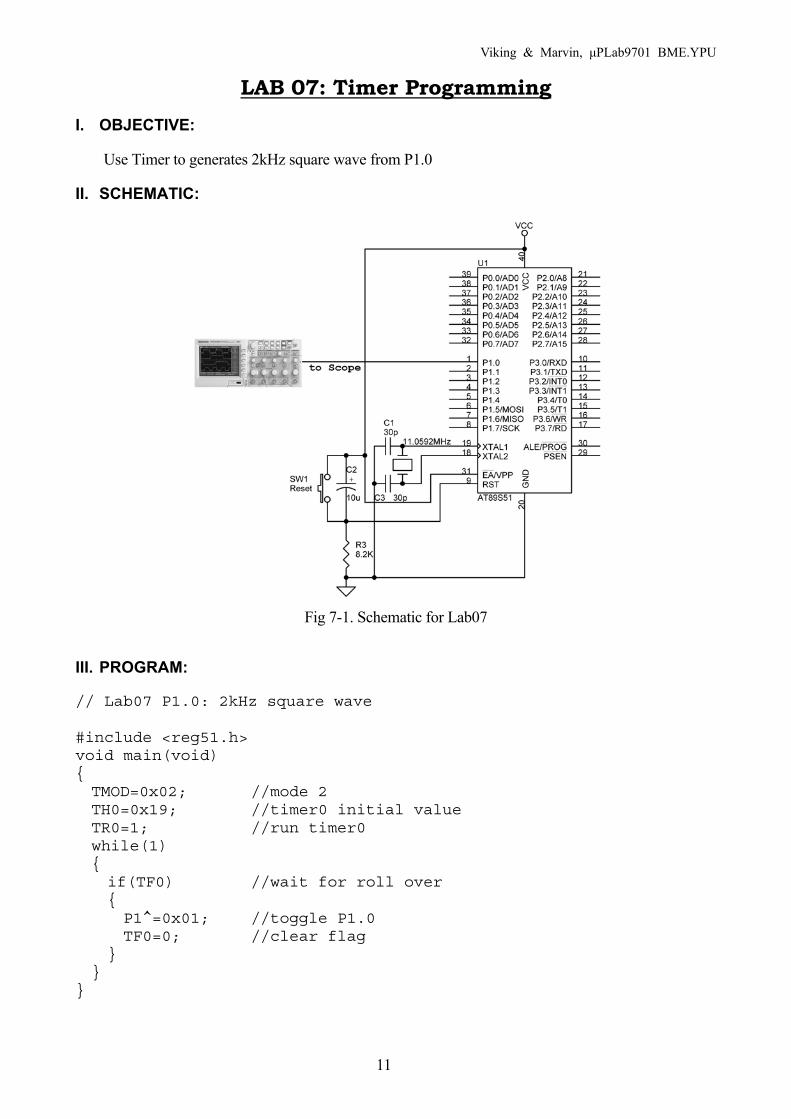
LAB 07: Timer Programming I. OBJECTIVE:
Use Timer to generates 2kHz square wave from P1.0
II. SCHEMATIC:
Fig 7-1. Schematic for Lab07
III. PROGRAM:
// Lab07 P1.0: 2kHz square wave #include <reg51.h> void main(void) TMOD=0x02; //mode 2 TH0=0x19; //timer0 initial value TR0=1; //run timer0 while(1) if(TF0) //wait for roll over P1^=0x01; //toggle P1.0 TF0=0; //clear flag
Viking & Marvin, μPLab9701 BME.YPU
12
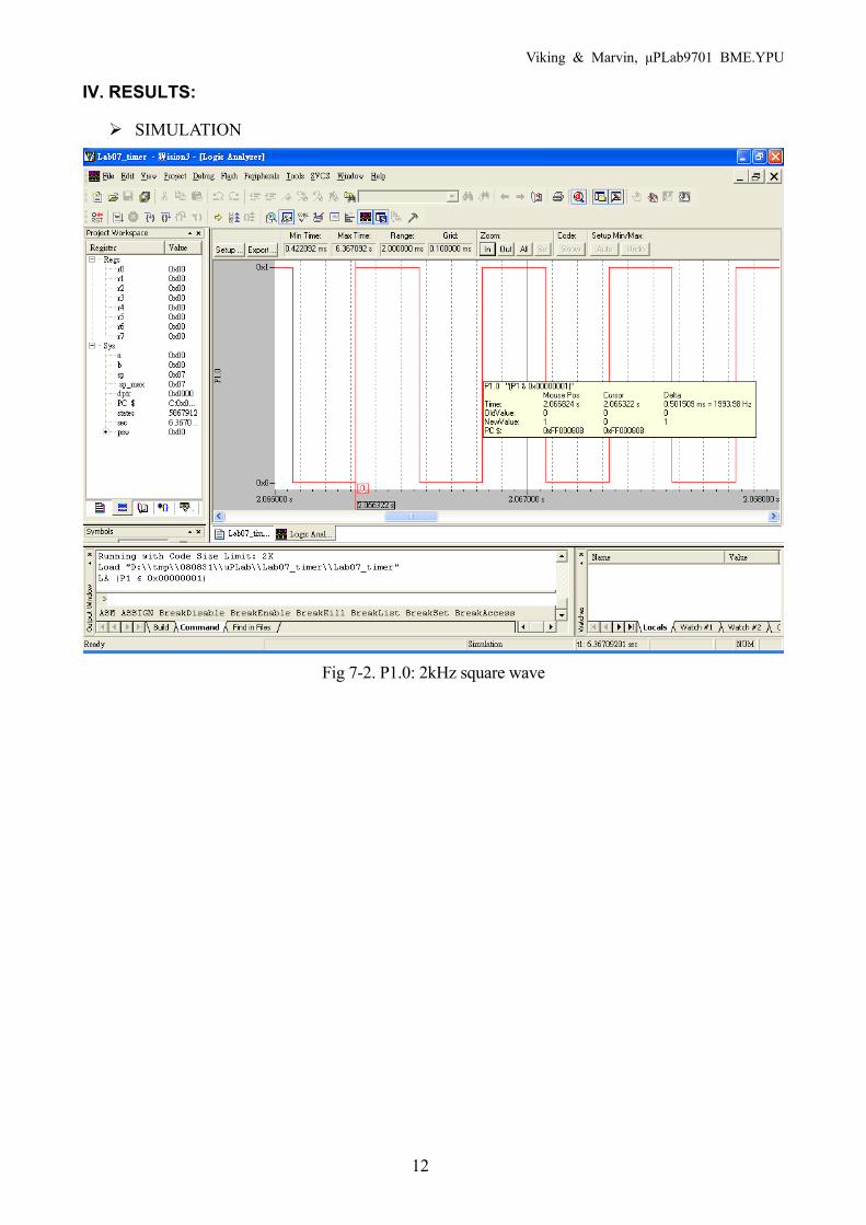
IV. RESULTS:
SIMULATION
Fig 7-2. P1.0: 2kHz square wave
Viking & Marvin, μPLab9701 BME.YPU
13
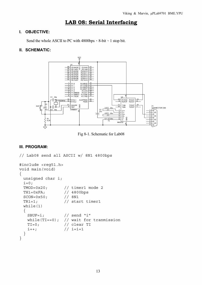
LAB 08: Serial Interfacing I. OBJECTIVE:
Send the whole ASCII to PC with 4800bps、8-bit、1 stop bit.
II. SCHEMATIC:
Fig 8-1. Schematic for Lab08
III. PROGRAM:
// Lab08 send all ASCII w/ 8N1 4800bps #include <reg51.h> void main(void) unsigned char i; i=0; TMOD=0x20; // timer1 mode 2 TH1=0xFA; // 4800bps SCON=0x50; // 8N1 TR1=1; // start timer1 while(1) SBUF=i; // send “i” while(TI==0); // wait for tranmission TI=0; // clear TI i++; // i=i+1
Viking & Marvin, μPLab9701 BME.YPU
14
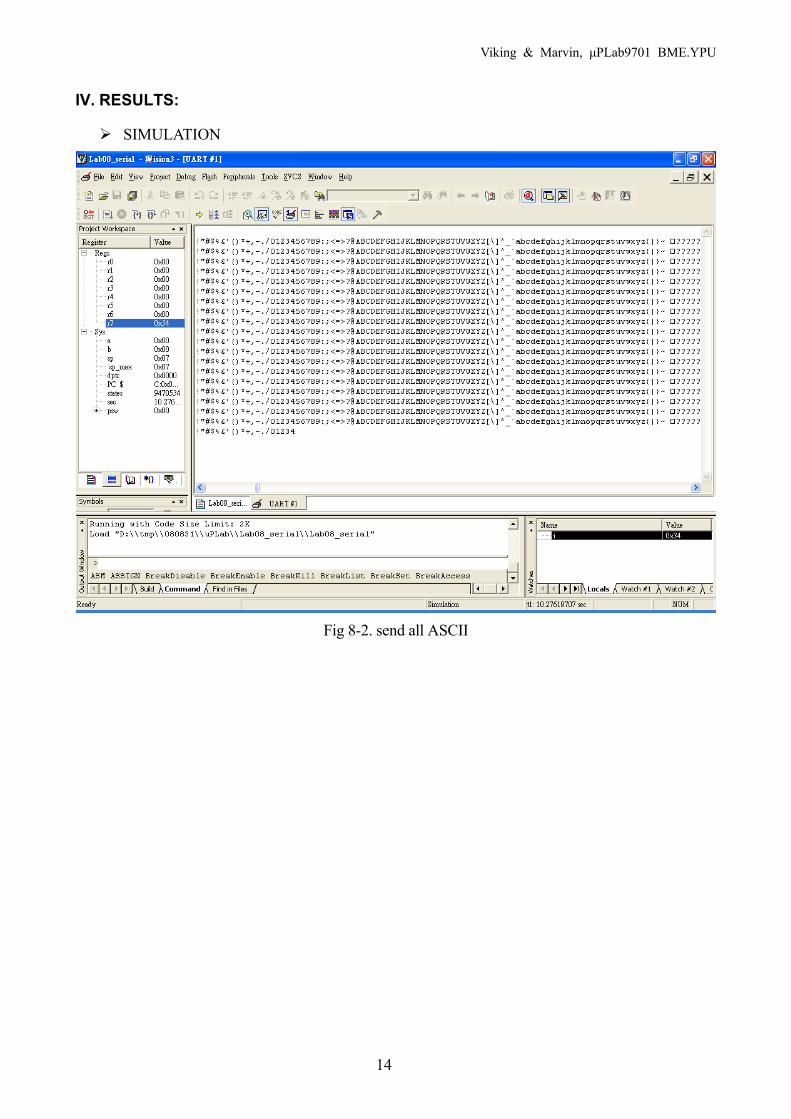
IV. RESULTS:
SIMULATION
Fig 8-2. send all ASCII

Viking & Marvin, μPLab9701 BME.YPU
15
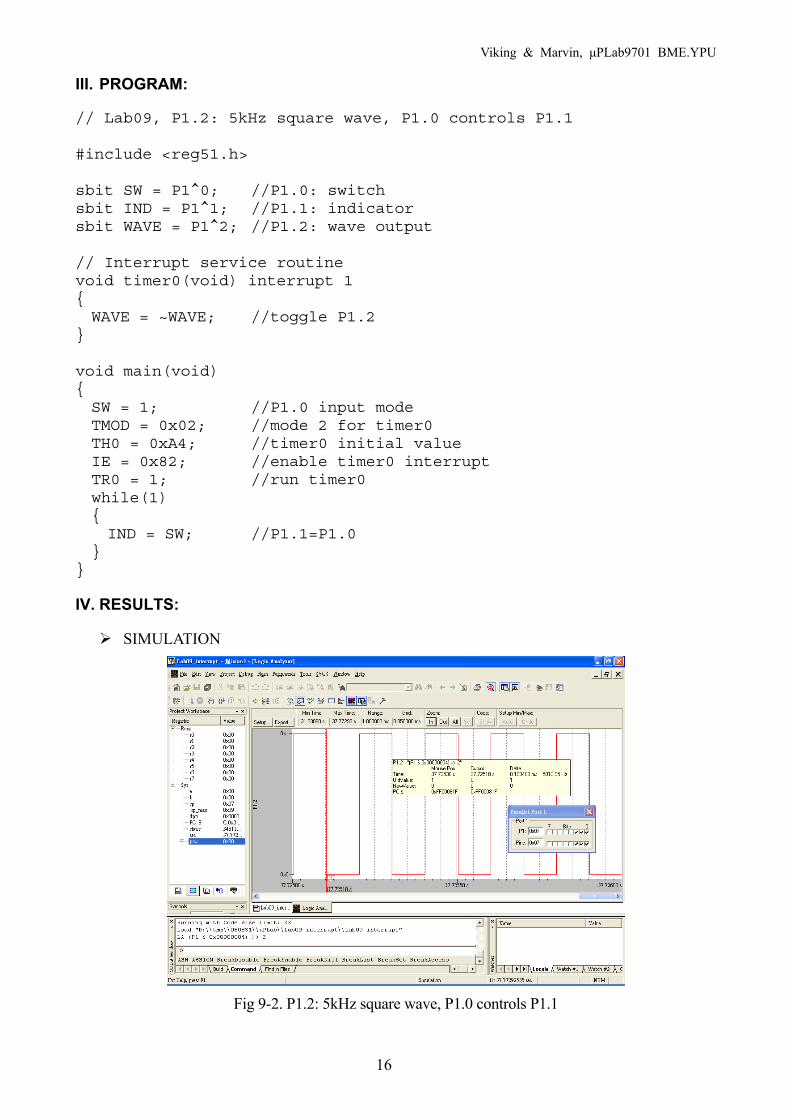
LAB 09: Interrupt Programming I. OBJECTIVE:
Generate 5kHz square wave from P1.2, and control P1.1 via P1.0.
II. SCHEMATIC:
Fig 9-1. Schematic for Lab09
Viking & Marvin, μPLab9701 BME.YPU
16
III. PROGRAM:
// Lab09, P1.2: 5kHz square wave, P1.0 controls P1.1 #include <reg51.h> sbit SW = P1^0; //P1.0: switch sbit IND = P1^1; //P1.1: indicator sbit WAVE = P1^2; //P1.2: wave output // Interrupt service routine void timer0(void) interrupt 1 WAVE = ~WAVE; //toggle P1.2 void main(void) SW = 1; //P1.0 input mode TMOD = 0x02; //mode 2 for timer0 TH0 = 0xA4; //timer0 initial value IE = 0x82; //enable timer0 interrupt TR0 = 1; //run timer0 while(1) IND = SW; //P1.1=P1.0
IV. RESULTS:
SIMULATION
Fig 9-2. P1.2: 5kHz square wave, P1.0 controls P1.1
Viking & Marvin, μPLab9701 BME.YPU
17
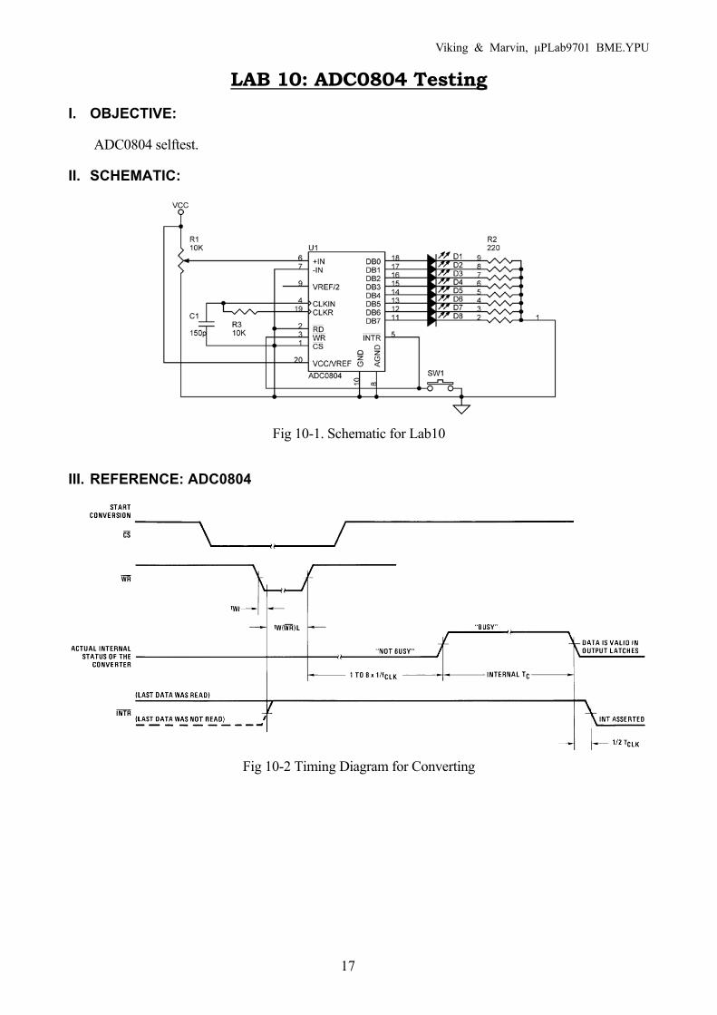
LAB 10: ADC0804 Testing I. OBJECTIVE:
ADC0804 selftest.
II. SCHEMATIC:
Fig 10-1. Schematic for Lab10
III. REFERENCE: ADC0804
Fig 10-2 Timing Diagram for Converting
Viking & Marvin, μPLab9701 BME.YPU
18
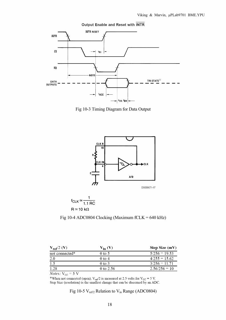
Fig 10-3 Timing Diagram for Data Output
Fig 10-4 ADC0804 Clocking (Maximum fCLK = 640 kHz)
Fig 10-5 Vref/2 Relation to Vin Range (ADC0804)
Viking & Marvin, μPLab9701 BME.YPU
19
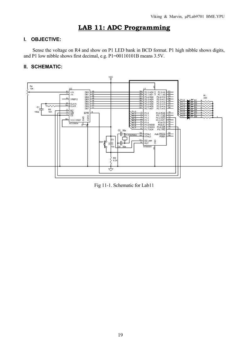
LAB 11: ADC Programming I. OBJECTIVE:
Sense the voltage on R4 and show on P1 LED bank in BCD format. P1 high nibble shows digits, and P1 low nibble shows first decimal, e.g. P1=00110101B means 3.5V.
II. SCHEMATIC:
Fig 11-1. Schematic for Lab11

Viking & Marvin, μPLab9701 BME.YPU
20
III. PROGRAM:
// Lab11, ADC0804 voltage sensing, show on P1 in BCD format // P1 high nibble shows digits // P1 low nibble shows first decimal // e.g. P1=00110101B means 3.5V #include <reg51.h> #include <absacc.h> //Include Macro Definitions unsigned char i; void bcd(unsigned char); void main(void) TCON |=0x01; //into edge trigger IE = 0x81; //enable int0 interrupt TCON |=0x02; //int0 1st request while(1); void int0(void) interrupt 0 i = XBYTE [0x0000]; //read from ADC bcd(i); XBYTE [0x0000] = 0; //another conversion void bcd(unsigned char j) unsigned int x; unsigned char y1,y2; x = j*10/51; y1 = x/10; y2 = x%10; y1 <<= 4; P1 = y1 + y2; //BCD data output
Viking & Marvin, μPLab9701 BME.YPU
21
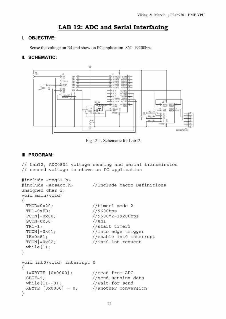
LAB 12: ADC and Serial Interfacing I. OBJECTIVE:
Sense the voltage on R4 and show on PC application. 8N1 19200bps
II. SCHEMATIC:
Fig 12-1. Schematic for Lab12
III. PROGRAM:
// Lab12, ADC0804 voltage sensing and serial transmission // sensed voltage is shown on PC application #include <reg51.h> #include <absacc.h> //Include Macro Definitions unsigned char i; void main(void) TMOD=0x20; //timer1 mode 2 TH1=0xFD; //9600bps PCON|=0x80; //9600*2=19200bps SCON=0x50; //8N1 TR1=1; //start timer1 TCON|=0x01; //into edge trigger IE=0x81; //enable int0 interrupt TCON|=0x02; //int0 1st request while(1); void int0(void) interrupt 0 i=XBYTE [0x0000]; //read from ADC SBUF=i; //send sensing data while(TI==0); //wait for send XBYTE [0x0000] = 0; //another conversion
Viking & Marvin, μPLab9701 BME.YPU
22
Appendix
A.1. SCHEDULE A.2. ELEMENTS & TOOLS A.3. LAB REPORT A.4. PC APPLICATIONS A.5. ORCAD/CAPTURE TUTORIAL A.6. KEIL μVISION C51 TUTORIAL A.7. K&H ICE TUTORIAL A.8. AT89S51 ISP TUTORIAL A.9. SUPER TERMINAL TUTORIAL A.10. ASCII A.11. C DATA TYPES AND OPERATORS
Viking & Marvin, μPLab9701 BME.YPU
23
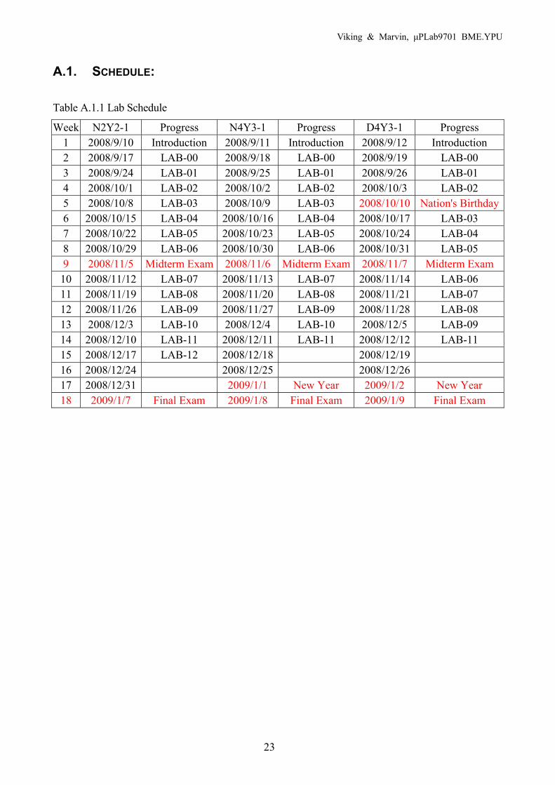
A.1. SCHEDULE:
Table A.1.1 Lab Schedule
Week N2Y2-1 Progress N4Y3-1 Progress D4Y3-1 Progress 1 2008/9/10 Introduction 2008/9/11 Introduction 2008/9/12 Introduction 2 2008/9/17 LAB-00 2008/9/18 LAB-00 2008/9/19 LAB-00 3 2008/9/24 LAB-01 2008/9/25 LAB-01 2008/9/26 LAB-01 4 2008/10/1 LAB-02 2008/10/2 LAB-02 2008/10/3 LAB-02 5 2008/10/8 LAB-03 2008/10/9 LAB-03 2008/10/10 Nation's Birthday6 2008/10/15 LAB-04 2008/10/16 LAB-04 2008/10/17 LAB-03 7 2008/10/22 LAB-05 2008/10/23 LAB-05 2008/10/24 LAB-04 8 2008/10/29 LAB-06 2008/10/30 LAB-06 2008/10/31 LAB-05 9 2008/11/5 Midterm Exam 2008/11/6 Midterm Exam 2008/11/7 Midterm Exam 10 2008/11/12 LAB-07 2008/11/13 LAB-07 2008/11/14 LAB-06 11 2008/11/19 LAB-08 2008/11/20 LAB-08 2008/11/21 LAB-07 12 2008/11/26 LAB-09 2008/11/27 LAB-09 2008/11/28 LAB-08 13 2008/12/3 LAB-10 2008/12/4 LAB-10 2008/12/5 LAB-09 14 2008/12/10 LAB-11 2008/12/11 LAB-11 2008/12/12 LAB-11 15 2008/12/17 LAB-12 2008/12/18 2008/12/19 16 2008/12/24 2008/12/25 2008/12/26 17 2008/12/31 2009/1/1 New Year 2009/1/2 New Year 18 2009/1/7 Final Exam 2009/1/8 Final Exam 2009/1/9 Final Exam
Viking & Marvin, μPLab9701 BME.YPU
24
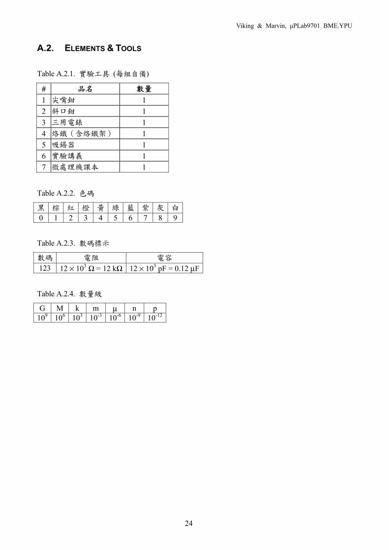
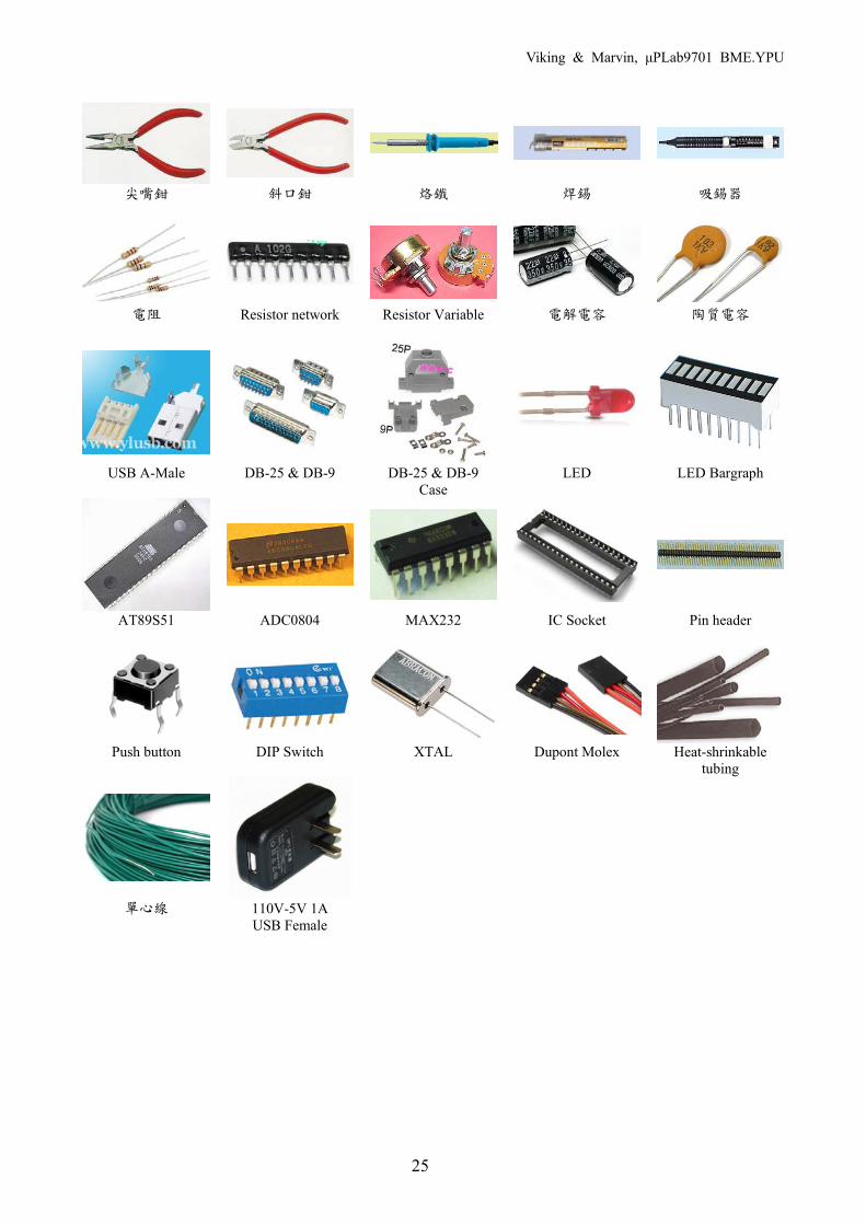
A.2. ELEMENTS & TOOLS
Table A.2.1. 實驗工具 (每組自備)
# 品名 數量 1 尖嘴鉗 1 2 斜口鉗 1 3 三用電錶 1 4 烙鐵(含烙鐵架) 1 5 吸錫器 1 6 實驗講義 1 7 微處理機課本 1
Table A.2.2. 色碼
黑 棕 紅 橙 黃 綠 藍 紫 灰 白
0 1 2 3 4 5 6 7 8 9
Table A.2.3. 數碼標示
數碼 電阻 電容 123 12 × 103 Ω = 12 kΩ 12 × 103 pF = 0.12 μF
Table A.2.4. 數量級
G M k m μ n p 109 106 103 10-3 10-6 10-9 10-12
Viking & Marvin, μPLab9701 BME.YPU
25
尖嘴鉗
斜口鉗
烙鐵
焊錫
吸錫器
電阻
Resistor network
Resistor Variable
電解電容
陶質電容
USB A-Male
DB-25 & DB-9
DB-25 & DB-9 Case
LED
LED Bargraph
AT89S51
ADC0804
MAX232
IC Socket
Pin header
Push button
DIP Switch
XTAL
Dupont Molex
Heat-shrinkable
tubing
單心線
110V-5V 1A USB Female
Viking & Marvin, μPLab9701 BME.YPU
26
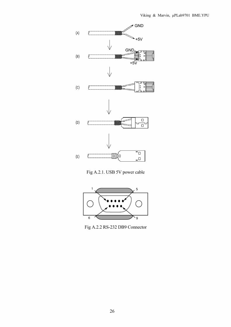
Fig A.2.1. USB 5V power cable
Fig A.2.2 RS-232 DB9 Connector
Viking & Marvin, μPLab9701 BME.YPU
27
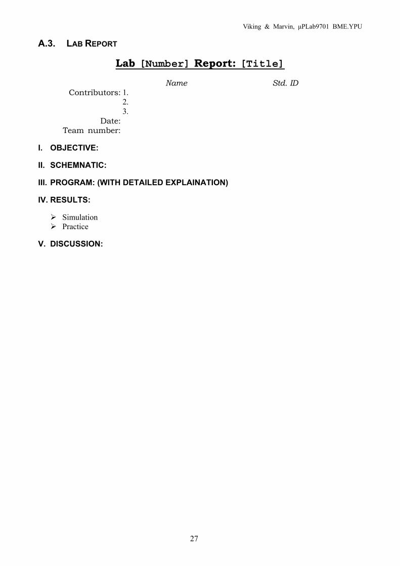
A.3. LAB REPORT
Lab [Number] Report: [Title] Name Std. ID
Contributors: 1. 2. 3.
Date: Team number:
I. OBJECTIVE:
II. SCHEMNATIC:
III. PROGRAM: (WITH DETAILED EXPLAINATION)
IV. RESULTS:
Simulation Practice
V. DISCUSSION:
Viking & Marvin, μPLab9701 BME.YPU
28
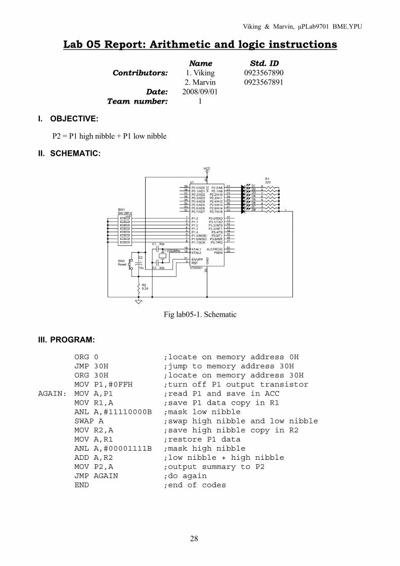
Lab 05 Report: Arithmetic and logic instructions Name Std. ID
Contributors: 1. Viking 0923567890 2. Marvin 0923567891
Date: 2008/09/01 Team number: 1
I. OBJECTIVE:
P2 = P1 high nibble + P1 low nibble
II. SCHEMATIC:
Fig lab05-1. Schematic
III. PROGRAM:
ORG 0 ;locate on memory address 0H JMP 30H ;jump to memory address 30H ORG 30H ;locate on memory address 30H MOV P1,#0FFH ;turn off P1 output transistor AGAIN: MOV A,P1 ;read P1 and save in ACC MOV R1,A ;save P1 data copy in R1 ANL A,#11110000B ;mask low nibble SWAP A ;swap high nibble and low nibble MOV R2,A ;save high nibble copy in R2 MOV A,R1 ;restore P1 data ANL A,#00001111B ;mask high nibble ADD A,R2 ;low nibble + high nibble MOV P2,A ;output summary to P2 JMP AGAIN ;do again END ;end of codes
Viking & Marvin, μPLab9701 BME.YPU
29
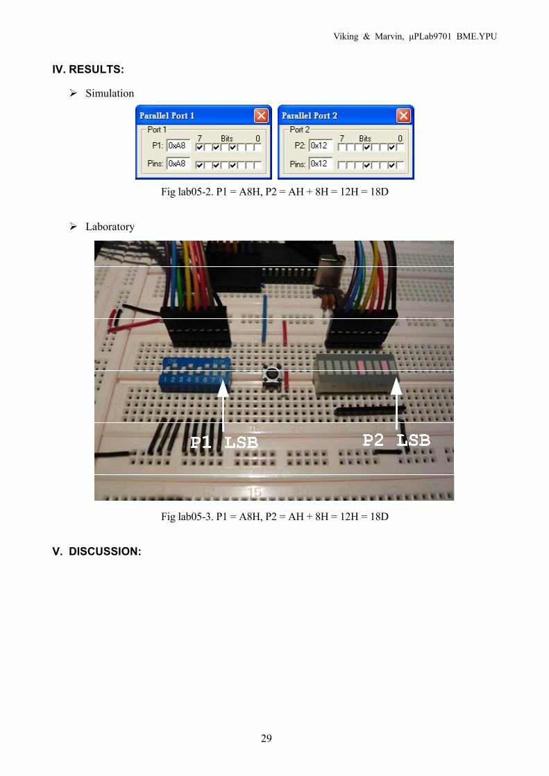
IV. RESULTS:
Simulation
Fig lab05-2. P1 = A8H, P2 = AH + 8H = 12H = 18D
Laboratory
Fig lab05-3. P1 = A8H, P2 = AH + 8H = 12H = 18D
V. DISCUSSION:

Viking & Marvin, μPLab9701 BME.YPU
30
A.4. PC APPLICATIONS
ORCAD/CAPTURE:
OrCAD: https://www.cadence.com/ Install OrCAD
Fig A.4.1. Warning for virus detection program
Fig A.4.2. Welcome message, Products selection

Viking & Marvin, μPLab9701 BME.YPU
31
Fig A.4.3. Directory assignment, Assign the folder name
Fig A.4.4. Start installation
Fig A.4.5. Installation progress
Viking & Marvin, μPLab9701 BME.YPU
32
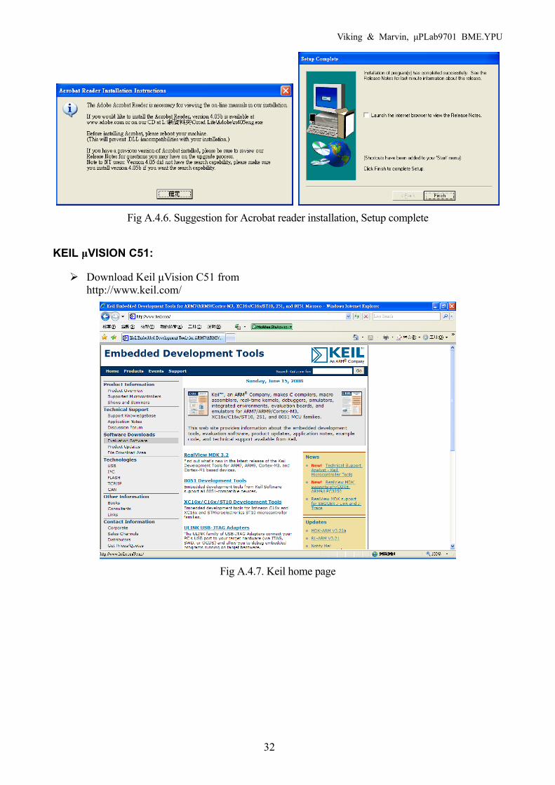
Fig A.4.6. Suggestion for Acrobat reader installation, Setup complete
KEIL μVISION C51:
Download Keil μVision C51 from http://www.keil.com/
Fig A.4.7. Keil home page
Viking & Marvin, μPLab9701 BME.YPU
33
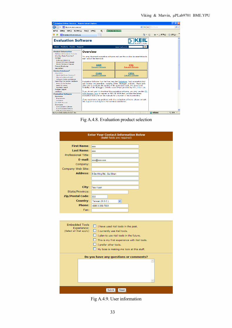
Fig A.4.8. Evaluation product selection
Fig A.4.9. User information
Viking & Marvin, μPLab9701 BME.YPU
34
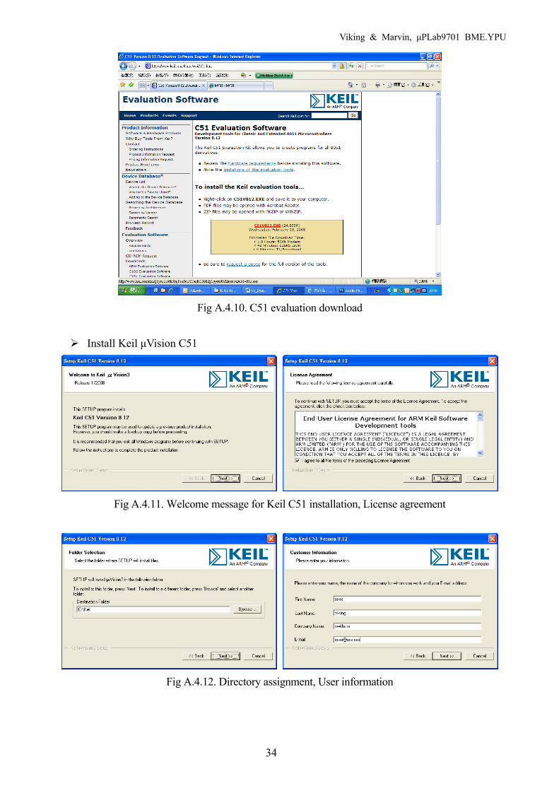
Fig A.4.10. C51 evaluation download
Install Keil μVision C51
Fig A.4.11. Welcome message for Keil C51 installation, License agreement
Fig A.4.12. Directory assignment, User information
Viking & Marvin, μPLab9701 BME.YPU
35
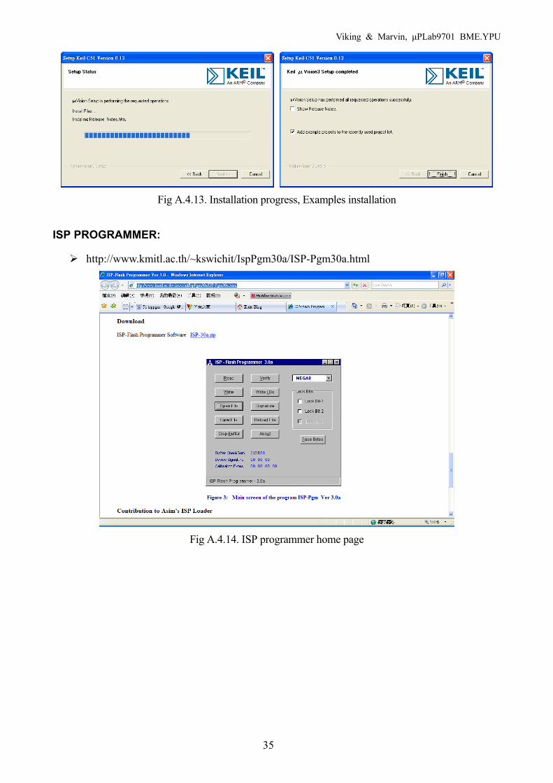
Fig A.4.13. Installation progress, Examples installation
ISP PROGRAMMER:
http://www.kmitl.ac.th/~kswichit/IspPgm30a/ISP-Pgm30a.html
Fig A.4.14. ISP programmer home page

Viking & Marvin, μPLab9701 BME.YPU
36
A.5. ORCAD/CAPTURE TUTORIAL
D8
D3D4
D1
D5
D2
D6
SW1SW DIP-8
U1
8051 ICE
9
1819
20
2930
31
40
12345678
2122232425262728
1011121314151617
3938373635343332
RST
XTAL2XTAL1
GN
D
PSENALE/PROG
EA/VPP
VCC
P1.0P1.1P1.2P1.3P1.4P1.5/MOSIP1.6/MISOP1.7/SCK
P2.0/A8P2.1/A9
P2.2/A10P2.3/A11P2.4/A12P2.5/A13P2.6/A14P2.7/A15
P3.0/RXDP3.1/TXD
P3.2/INT0P3.3/INT1
P3.4/T0P3.5/T1
P3.6/WRP3.7/RD
P0.0/AD0P0.1/AD1P0.2/AD2P0.3/AD3P0.4/AD4P0.5/AD5P0.6/AD6P0.7/AD7
D7
R1220
123456789
Fig A.5.1. Example schematic
Fig A.5.2. OrCAD capture
Viking & Marvin, μPLab9701 BME.YPU
37
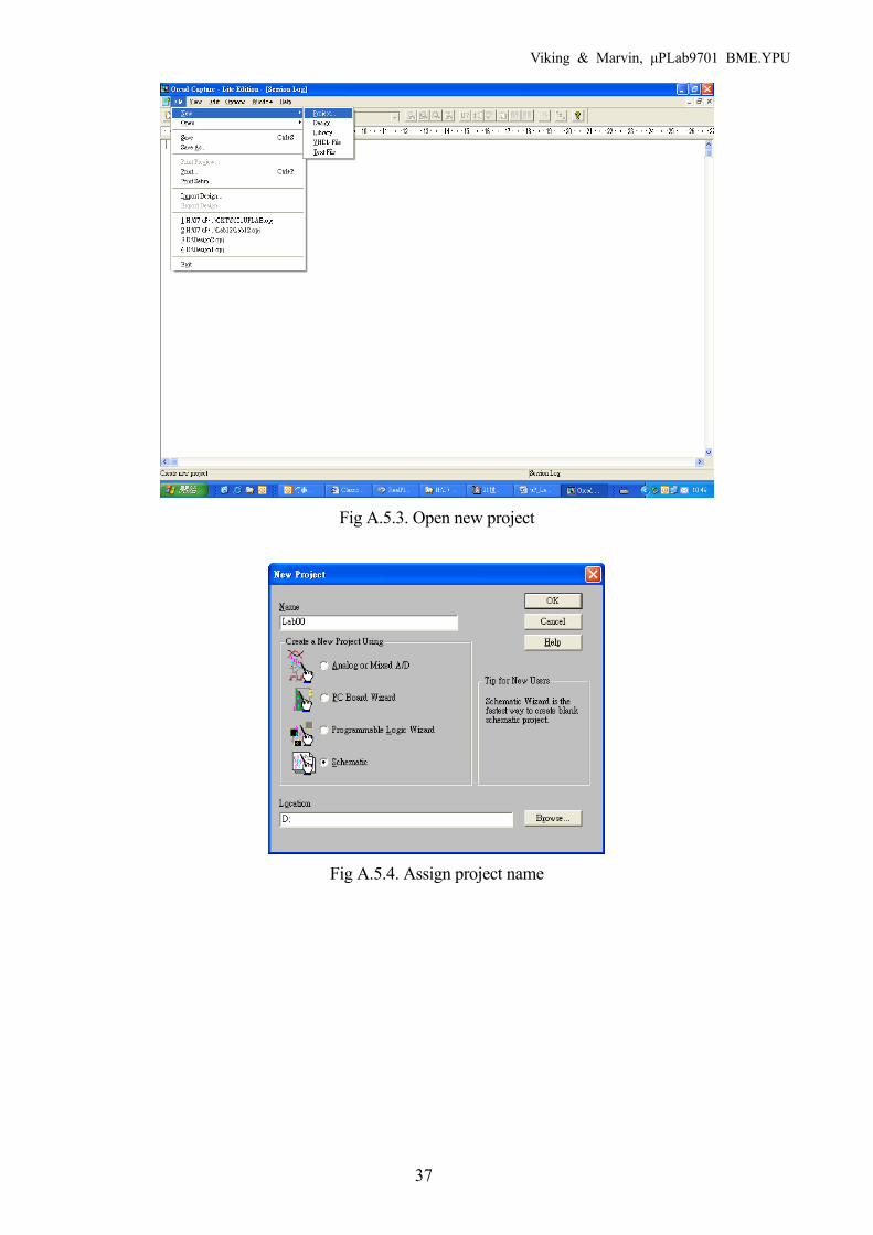
Fig A.5.3. Open new project
Fig A.5.4. Assign project name
Viking & Marvin, μPLab9701 BME.YPU
38
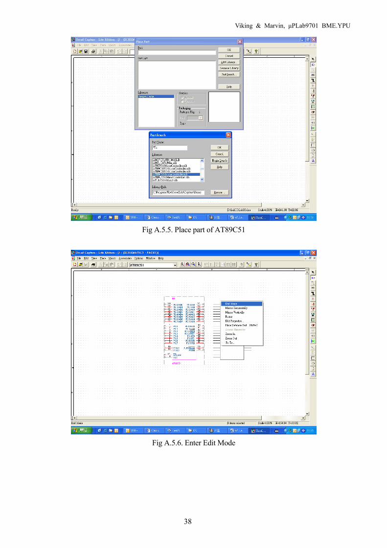
Fig A.5.5. Place part of AT89C51
Fig A.5.6. Enter Edit Mode
Viking & Marvin, μPLab9701 BME.YPU
39
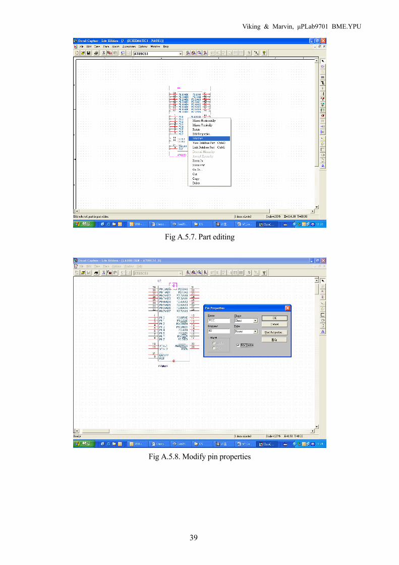
Fig A.5.7. Part editing
Fig A.5.8. Modify pin properties
Viking & Marvin, μPLab9701 BME.YPU
40
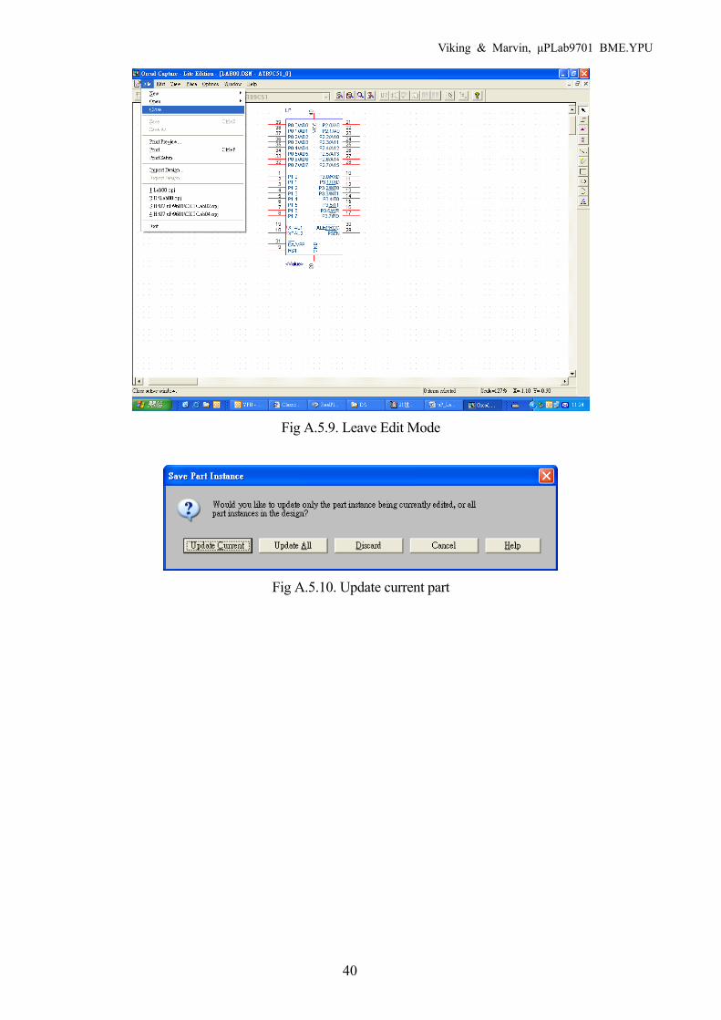
Fig A.5.9. Leave Edit Mode
Fig A.5.10. Update current part

Viking & Marvin, μPLab9701 BME.YPU
41
Fig A.5.11. Place part of LED
Fig A.5.12. Place part of Resistor SIP
Viking & Marvin, μPLab9701 BME.YPU
42
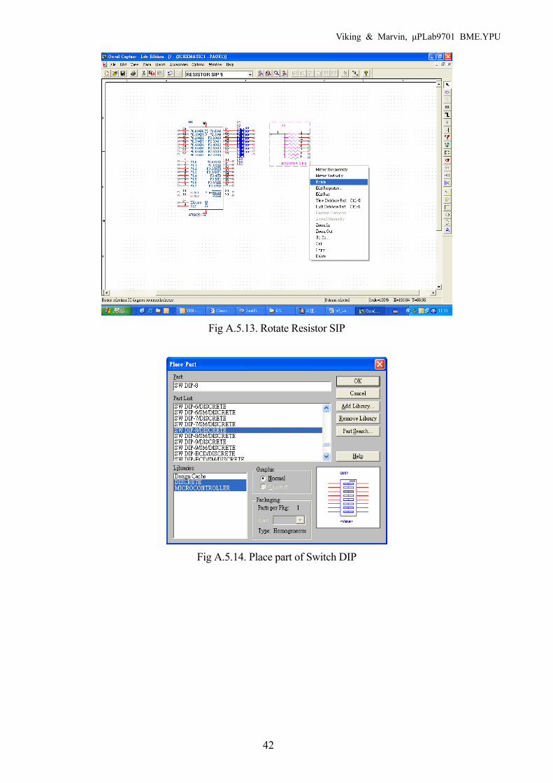
Fig A.5.13. Rotate Resistor SIP
Fig A.5.14. Place part of Switch DIP

Viking & Marvin, μPLab9701 BME.YPU
43
Fig A.5.15. Place the Wire

Viking & Marvin, μPLab9701 BME.YPU
44
A.6. KEIL μVISION C51 TUTORIAL
Fig A.6.1. Schematic for μVision tutorial
MOV P1,#0FFH ;set P1 input mode AGAIN: MOV A,P1 ;move data from P1 to A MOV P2,A ;output data from A to P2 JMP AGAIN ;jump back to AGAIN END ;end of coding
Fig A.6.2. Initiates Keil μVision C51
Viking & Marvin, μPLab9701 BME.YPU
45
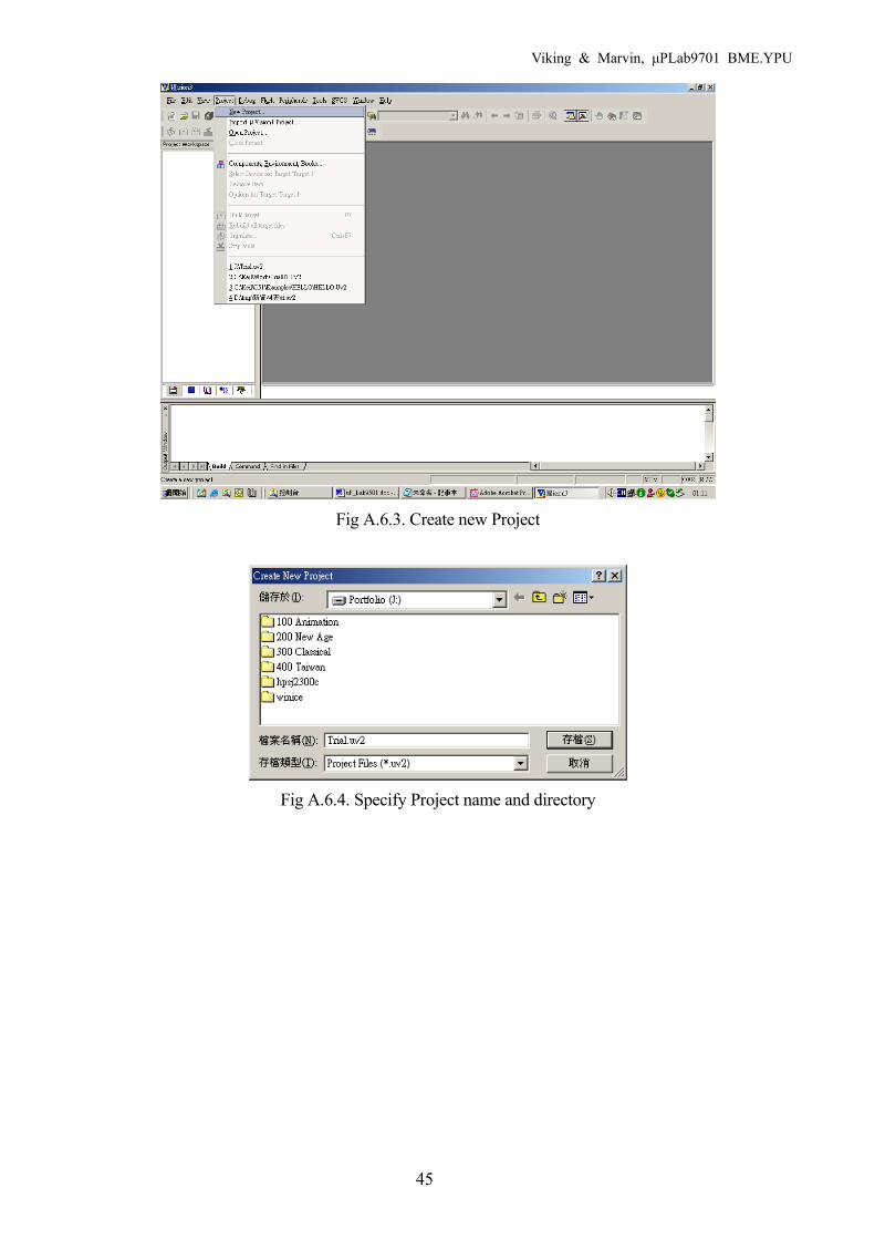
Fig A.6.3. Create new Project
Fig A.6.4. Specify Project name and directory

Viking & Marvin, μPLab9701 BME.YPU
46
Fig A.6.5. Specify Vendor
Fig A.6.6. Specify model number
Fig A.6.7. Copy Startup codes or “not”
Viking & Marvin, μPLab9701 BME.YPU
47
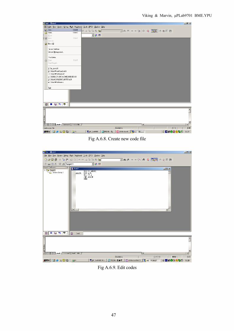
Fig A.6.8. Create new code file
Fig A.6.9. Edit codes
Viking & Marvin, μPLab9701 BME.YPU
48
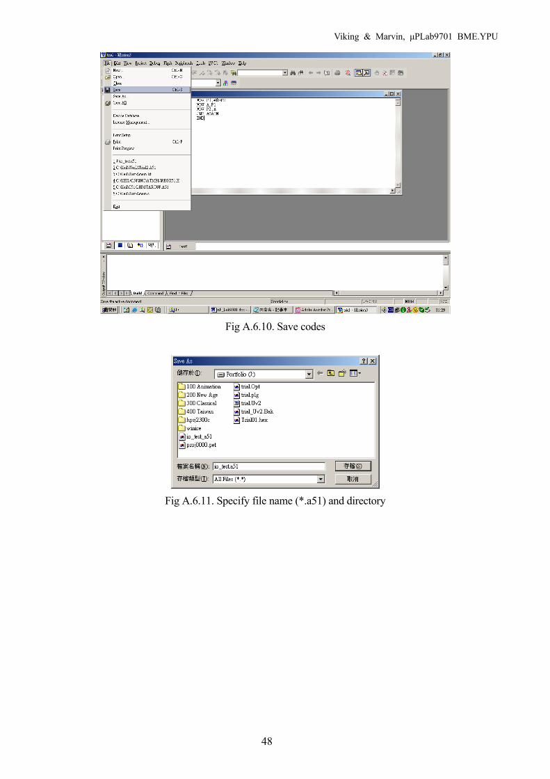
Fig A.6.10. Save codes
Fig A.6.11. Specify file name (*.a51) and directory
Viking & Marvin, μPLab9701 BME.YPU
49
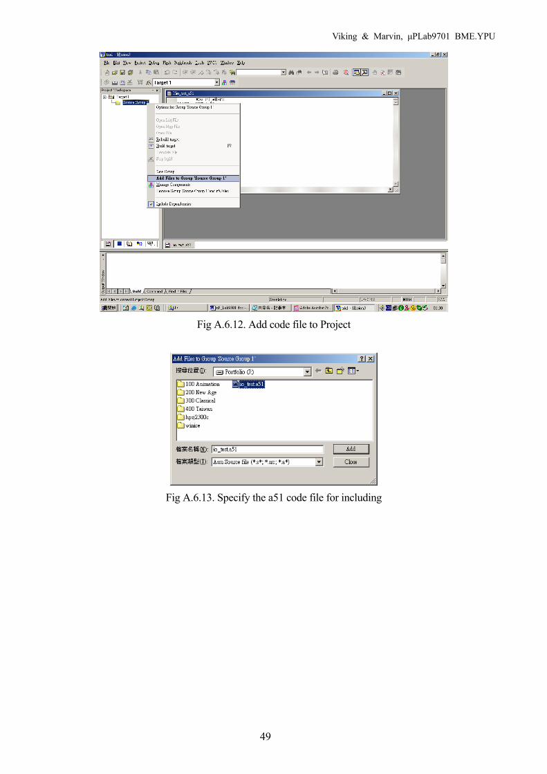
Fig A.6.12. Add code file to Project
Fig A.6.13. Specify the a51 code file for including
Viking & Marvin, μPLab9701 BME.YPU
50
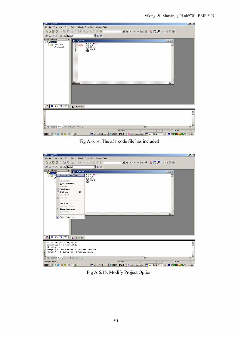
Fig A.6.14. The a51 code file has included
Fig A.6.15. Modify Project Option
Viking & Marvin, μPLab9701 BME.YPU
51
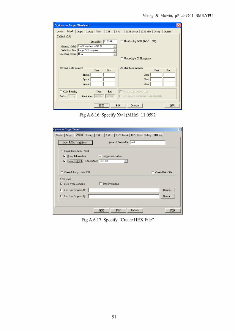
Fig A.6.16. Specify Xtal (MHz): 11.0592
Fig A.6.17. Specify “Create HEX File”

Viking & Marvin, μPLab9701 BME.YPU
52
Fig A.6.18. Build Target
Fig A.6.19. Start Debug Session (Simulation)
Viking & Marvin, μPLab9701 BME.YPU
53
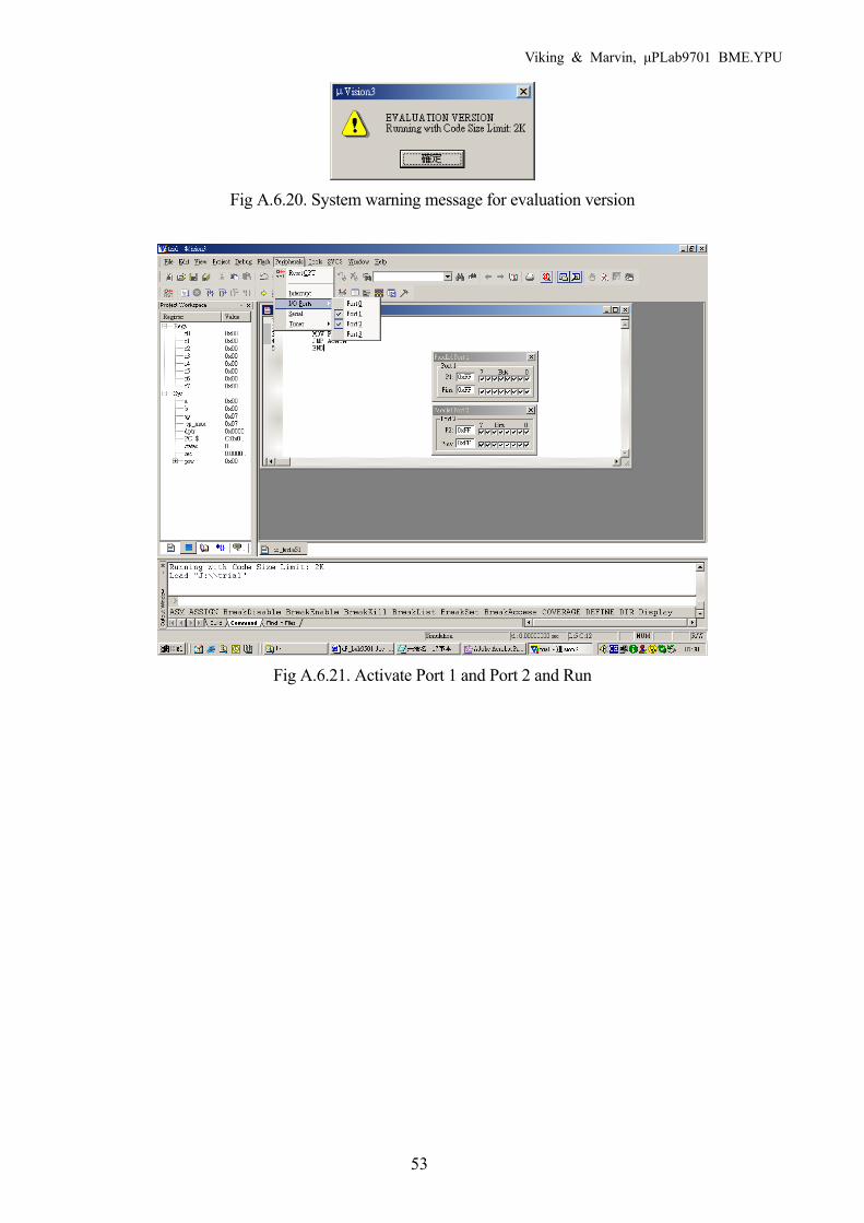
Fig A.6.20. System warning message for evaluation version
Fig A.6.21. Activate Port 1 and Port 2 and Run
Viking & Marvin, μPLab9701 BME.YPU
54
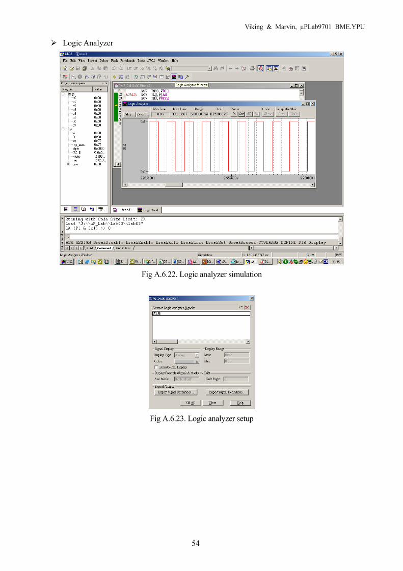
Logic Analyzer
Fig A.6.22. Logic analyzer simulation
Fig A.6.23. Logic analyzer setup
Viking & Marvin, μPLab9701 BME.YPU
55
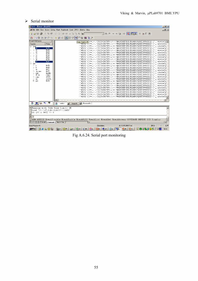
Serial monitor
Fig A.6.24. Serial port monitoring
Viking & Marvin, μPLab9701 BME.YPU
56
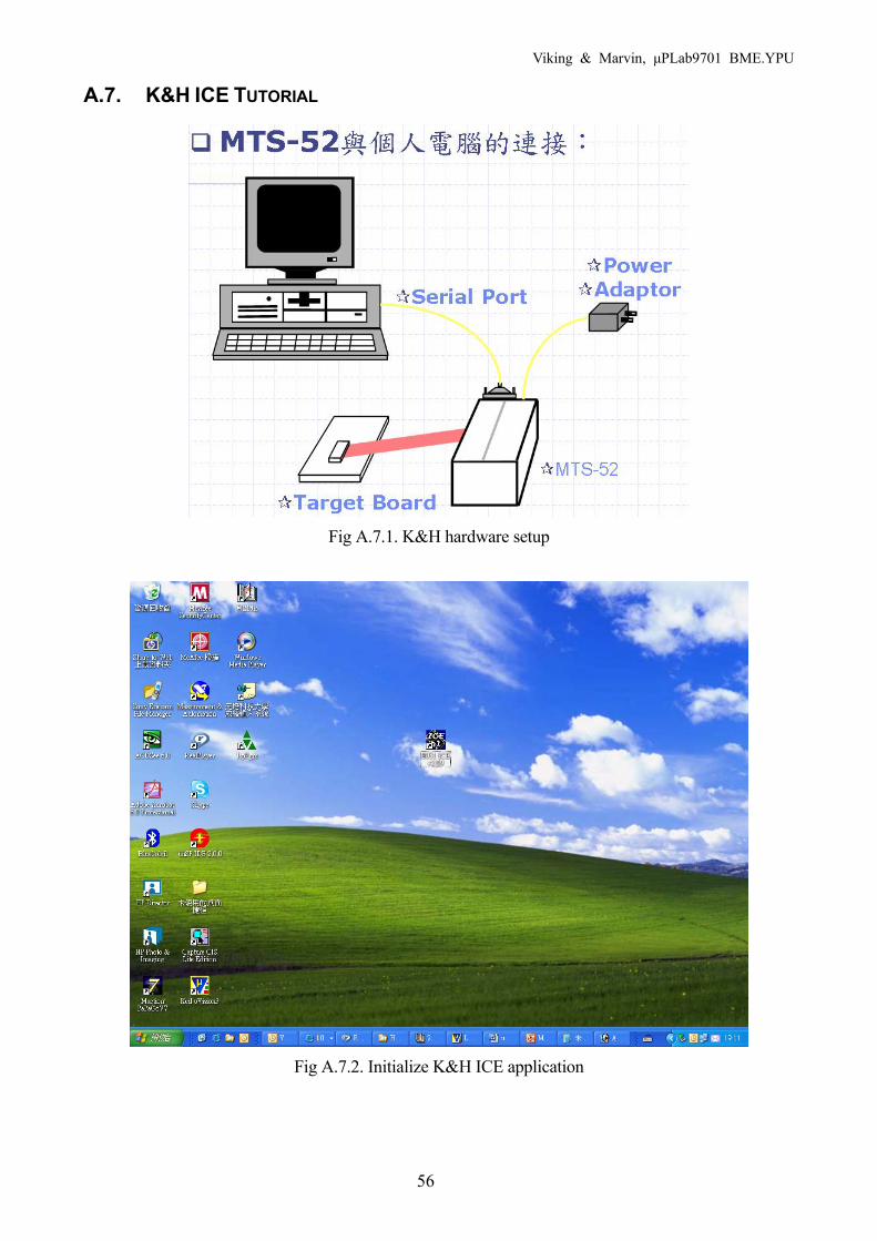
A.7. K&H ICE TUTORIAL
Fig A.7.1. K&H hardware setup
Fig A.7.2. Initialize K&H ICE application
Viking & Marvin, μPLab9701 BME.YPU
57
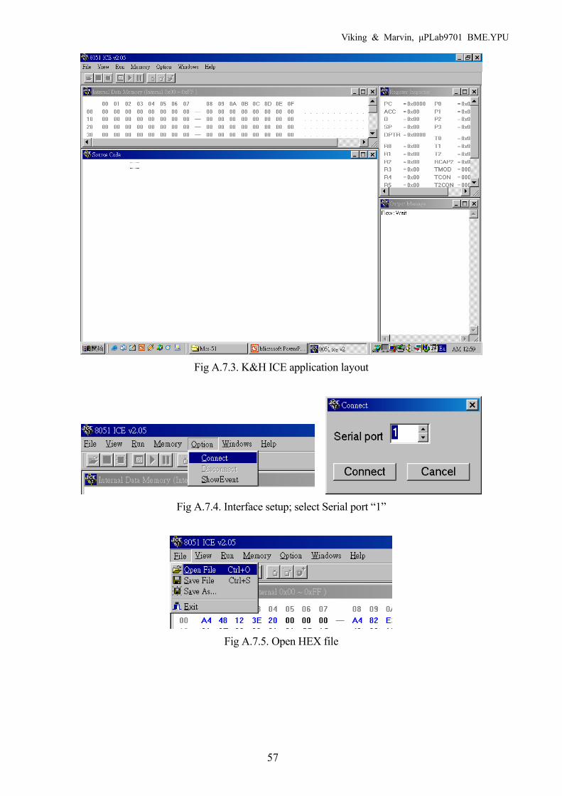
Fig A.7.3. K&H ICE application layout
Fig A.7.4. Interface setup; select Serial port “1”
Fig A.7.5. Open HEX file

Viking & Marvin, μPLab9701 BME.YPU
58
Fig A.7.6. HEX file selection
Fig A.7.7. HEX file loaded
Fig A.7.8. Tool bar
Viking & Marvin, μPLab9701 BME.YPU
59
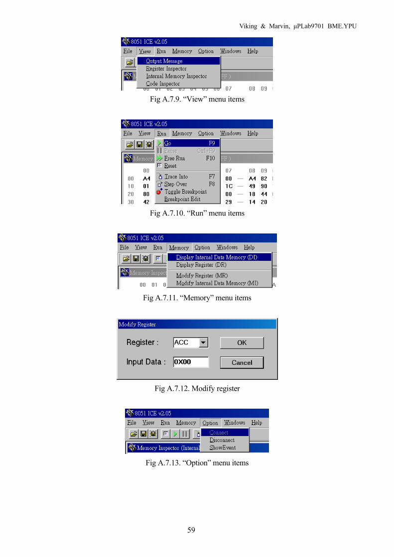
Fig A.7.9. “View” menu items
Fig A.7.10. “Run” menu items
Fig A.7.11. “Memory” menu items
Fig A.7.12. Modify register
Fig A.7.13. “Option” menu items

Viking & Marvin, μPLab9701 BME.YPU
60
建議將主程式的起始位置放在位址 0050H 之後,換句話說,建議將程式開頭寫成以下的形
式: ORG 0000H JMP MAIN ORG 0050H MAIN: ... ...
Viking & Marvin, μPLab9701 BME.YPU
61
A.8. AT89S51 ISP TUTORIAL
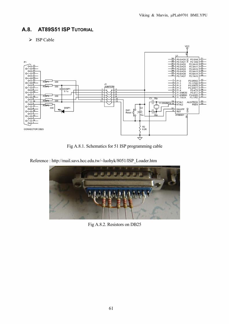
ISP Cable
Fig A.8.1. Schematics for 51 ISP programming cable
Reference : http://mail.savs.hcc.edu.tw/~luohyk/8051/ISP_Loader.htm
Fig A.8.2. Resistors on DB25
Viking & Marvin, μPLab9701 BME.YPU
62
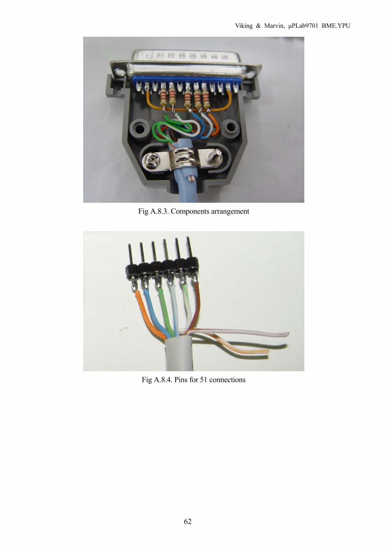
Fig A.8.3. Components arrangement
Fig A.8.4. Pins for 51 connections
Viking & Marvin, μPLab9701 BME.YPU
63
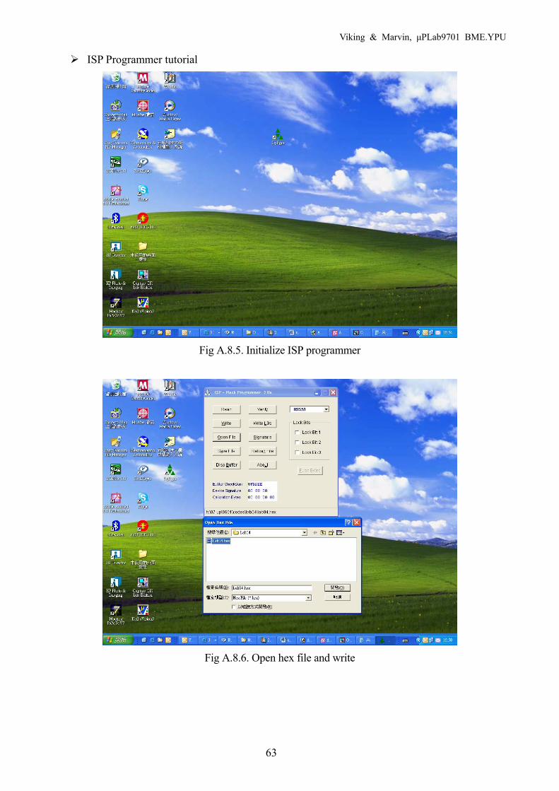
ISP Programmer tutorial
Fig A.8.5. Initialize ISP programmer
Fig A.8.6. Open hex file and write
Viking & Marvin, μPLab9701 BME.YPU
64
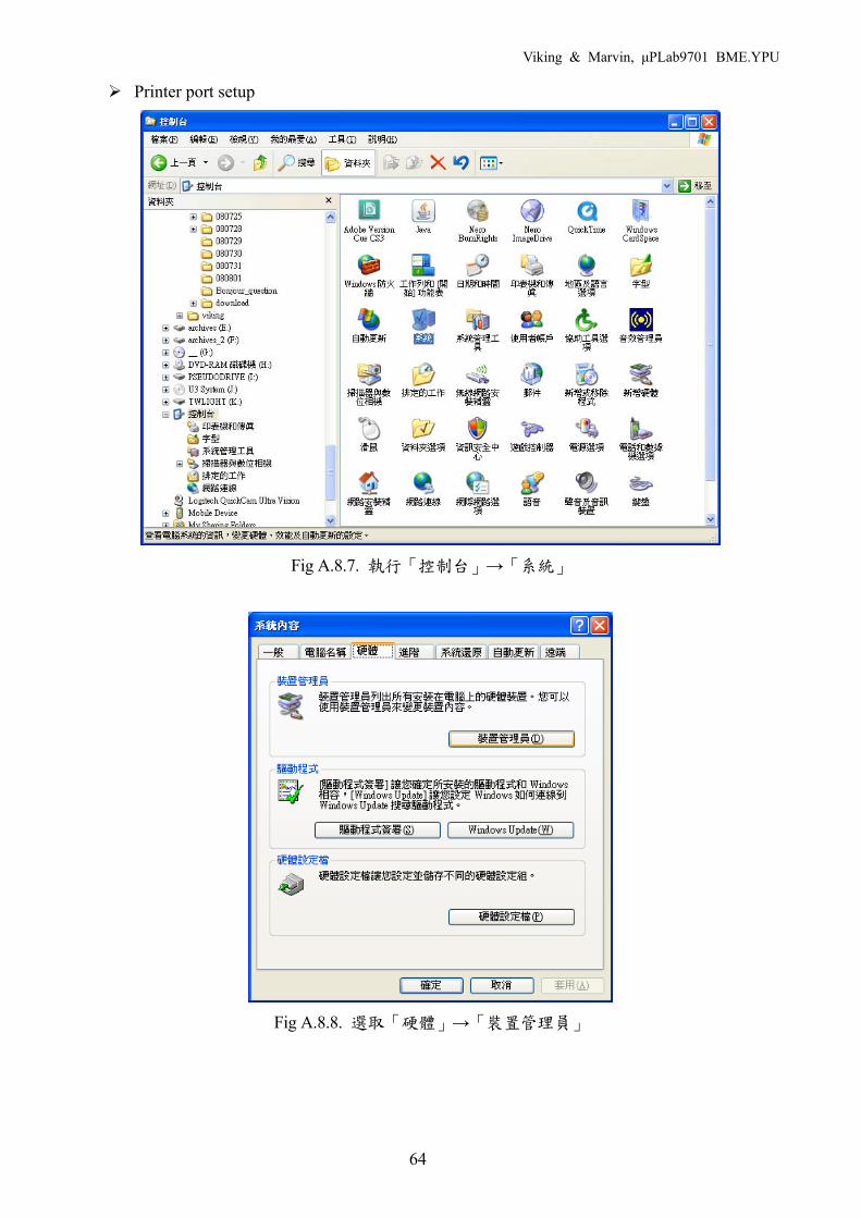
Printer port setup
Fig A.8.7. 執行「控制台」→「系統」
Fig A.8.8. 選取「硬體」→「裝置管理員」
Viking & Marvin, μPLab9701 BME.YPU
65
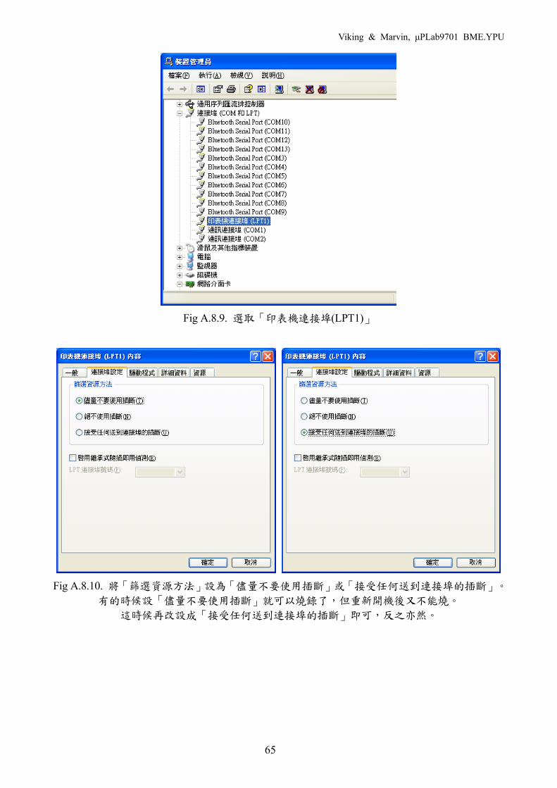
Fig A.8.9. 選取「印表機連接埠(LPT1)」
Fig A.8.10. 將「篩選資源方法」設為「儘量不要使用插斷」或「接受任何送到連接埠的插斷」。
有的時候設「儘量不要使用插斷」就可以燒錄了,但重新開機後又不能燒。 這時候再改設成「接受任何送到連接埠的插斷」即可,反之亦然。
Viking & Marvin, μPLab9701 BME.YPU
66
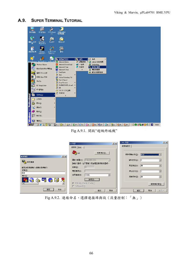
A.9. SUPER TERMINAL TUTORIAL
Fig A.9.1. 開啟“超級終端機”
Fig A.9.2. 連線命名、選擇連接埠與設(流量控制:「無」)

Viking & Marvin, μPLab9701 BME.YPU
67
Fig A.9.3. 設定「回應輸入的字元」
Viking & Marvin, μPLab9701 BME.YPU
68
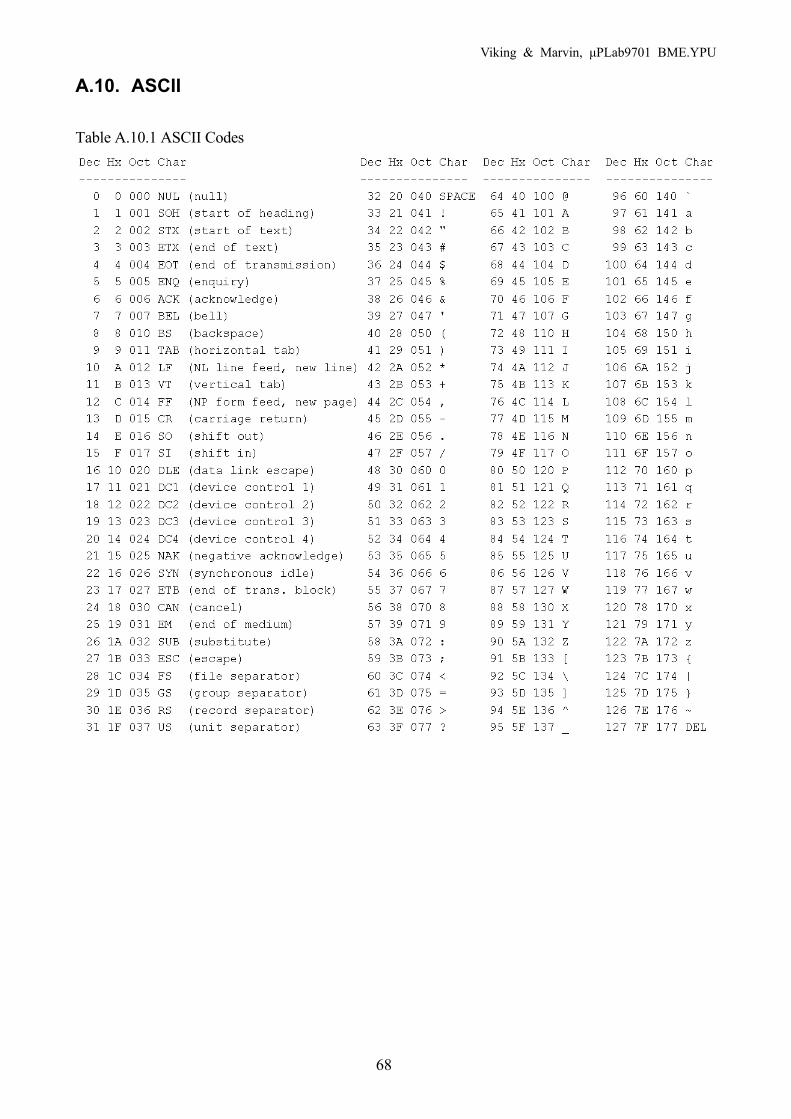
A.10. ASCII
Table A.10.1 ASCII Codes
Viking & Marvin, μPLab9701 BME.YPU
69
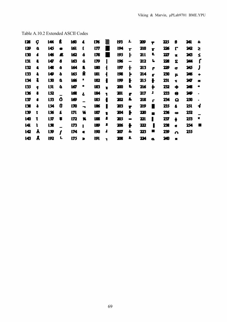
Table A.10.2 Extended ASCII Codes
Viking & Marvin, μPLab9701 BME.YPU
70
A.11. C DATA TYPES AND OPERATORS
Basing on Wikipedia, the free encyclopedia http://en.wikipedia.org/wiki/Operators_in_C_and_C%2B%2B
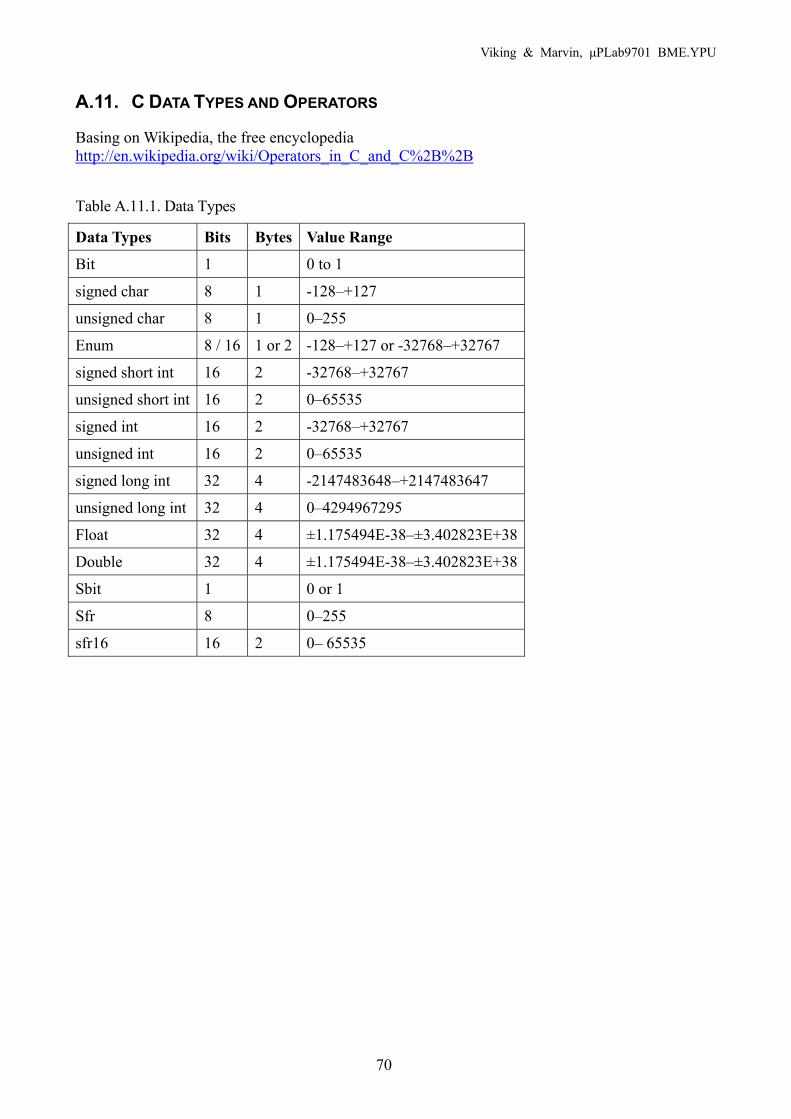
Table A.11.1. Data Types
Data Types Bits Bytes Value Range
Bit 1 0 to 1
signed char 8 1 -128–+127
unsigned char 8 1 0–255
Enum 8 / 16 1 or 2 -128–+127 or -32768–+32767
signed short int 16 2 -32768–+32767
unsigned short int 16 2 0–65535
signed int 16 2 -32768–+32767
unsigned int 16 2 0–65535
signed long int 32 4 -2147483648–+2147483647
unsigned long int 32 4 0–4294967295
Float 32 4 ±1.175494E-38–±3.402823E+38
Double 32 4 ±1.175494E-38–±3.402823E+38
Sbit 1 0 or 1
Sfr 8 0–255
sfr16 16 2 0– 65535
Viking & Marvin, μPLab9701 BME.YPU
71
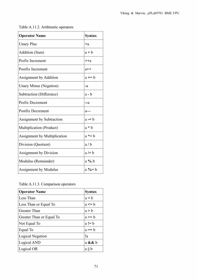
Table A.11.2. Arithmetic operators
Operator Name Syntax
Unary Plus +a
Addition (Sum) a + b
Prefix Increment ++a
Postfix Increment a++
Assignment by Addition a += b
Unary Minus (Negation) -a
Subtraction (Difference) a - b
Prefix Decrement --a
Postfix Decrement a—
Assignment by Subtraction a -= b
Multiplication (Product) a * b
Assignment by Multiplication a *= b
Division (Quotient) a / b
Assignment by Division a /= b
Modulus (Remainder) a % b
Assignment by Modulus a %= b
Table A.11.3. Comparison operators
Operator Name Syntax Less Than a < b Less Than or Equal To a <= b Greater Than a > b Greater Than or Equal To a >= b Not Equal To a != b Equal To a == b Logical Negation !a Logical AND a && b Logical OR a || b
Viking & Marvin, μPLab9701 BME.YPU
72
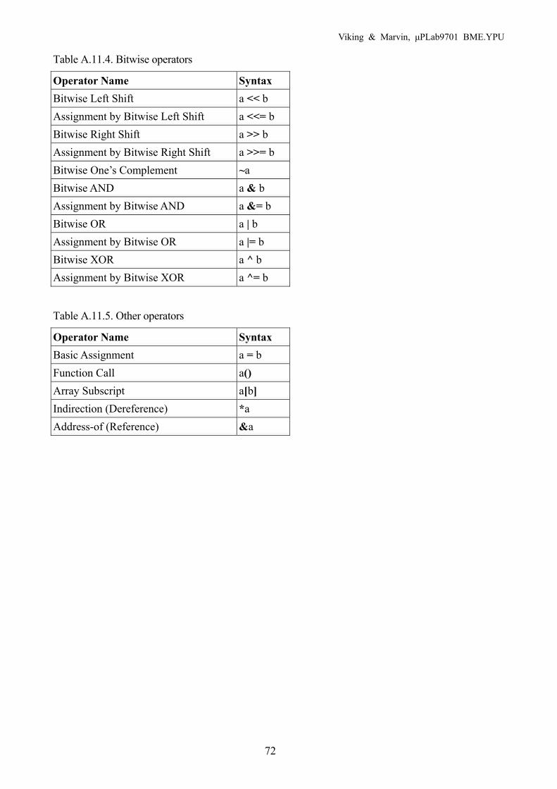
Table A.11.4. Bitwise operators
Operator Name Syntax Bitwise Left Shift a << b Assignment by Bitwise Left Shift a <<= b Bitwise Right Shift a >> b Assignment by Bitwise Right Shift a >>= b Bitwise One’s Complement ~a Bitwise AND a & b Assignment by Bitwise AND a &= b Bitwise OR a | b Assignment by Bitwise OR a |= b Bitwise XOR a ^ b Assignment by Bitwise XOR a ^= b
Table A.11.5. Other operators
Operator Name Syntax Basic Assignment a = b Function Call a() Array Subscript a[b] Indirection (Dereference) *a Address-of (Reference) &a