Embed Size (px)
Citation preview
A layout and simulation tool for deep sub-micron CMOS design
MICROWIND & DSCH
User's Manual
Version 3.5
© Copyright 1997-2010 by INSA Toulouse, University of Toulouse, FRANCE


MICROWIND & DSCH V3.5 - USER'S MANUAL
3
About the author
Etienne SICARD was born in Paris, France, June 1961. He received the B.S degree
in 1984 and the PhD in Electrical Engineering from the University of Toulouse, in
1987, in the laboratory LAAS of Toulouse. He was granted a Monbusho scholarship
and stayed 18 months at Osaka University, Japan (1988-1989). Previously a
professor of electronics in the Department of Physics, University of Balearic
Islands, Spain (1990), Etienne SICARD is currently a professor at INSA of
Toulouse, France, Department of Electrical and Computer Engineering. He is a
visiting professor at the electronic department of Carleton University, Ottawa, in
2004. His research interests include several aspects of integrated circuits (ICs) for improved electromagnetic
compatibility (EMC), and the development of tools for speech processing applied to speech therapy.
Etienne SICARD is the author of several books, as well as software for CMOS design (Microwind), EMC
of ICs signal processing (MentorDSP), speech therapy (Vocalab) and EMC of integrated circuits (IC-EMC).
He is a member of French SEE and senior member of the IEEE EMC society. He was elected in 2006
distinguished IEEE lecturer for EMC of ICs.
Email: [email protected]
Support and Feedback
Please report problems or suggestions to:
Copyright
© Copyright 1997-2010 by INSA Toulouse, University of Toulouse, FRANCE
ISBN
ISBN (13 numbers) : 978-2-87649-057-4
Published by INSA Toulouse
University of Toulouse
135 Av de Rangueil
31077 Toulouse - France
First print : October 2009
Legal deposit : October 2009
MICROWIND & DSCH V3.5 - USER'S MANUAL
4
Books Using Microwind
“Chip Design for Submicron VLSI: CMOS Layout and Simulation” by John Uyemura - Georgia Institute of Technology, USA - http://www.engineering.thomsonlearning.com 2005, IBSN 053446629X
“Basic CMOS cell Design” by Etienne Sicard and Sonia Bendhia, McGraw-Hill India, 2005, ISBN 0-07-059933-5 (only available in India)
A book about design of CMOS integrated circuits in deep submicron technologies, based on Microwind and DSCH, written by Etienne SICARD and Sonia BEN DHIA. McGraw-Hill professional series, USA, Jan. 2007, ISBN: 007148839, DOI:10.1036/0071488391
This book is about advanced design of CMOS integrated circuits in deep submicron technologies. It deals with microprocessors, embedded memories, RF cells, converters; FPGAs, packaging, SOI and future. McGraw-Hill professional series, Jan. 2007, ISBN: 0071488367, DOI:10.1036/0071488367
Web information
• www.microwind.org for general information about MICROWIND
• www.microwind.net to download the lite version and order the professional version
About ni2designs
ni2designs develop, design, manufacture and market a broad range of EDA tools and complete system
solutions targeted at worldwide audience. Their diverse product portfolio serves applications in
Microelectronics, VLSI, Embedded Systems, DSP, Modeling & Simulation, and EM & Antenna Designs.
Head Office:
ni logic Pvt. Ltd.,
Pune, India
Tele-Fax : +91-20-25286947 / 8
Email : [email protected]
URL : www.ni2designs.com

MICROWIND & DSCH V3.5 - USER'S MANUAL
5
Table of Contents
About the author...................................................................................................................................................... 3 Support and Feedback ............................................................................................................................................. 3 Please report problems or suggestions to: ............................................................................................................... 3 [email protected] .......................................................................................................................................... 3 Copyright ................................................................................................................................................................. 3 ISBN........................................................................................................................................................................ 3 Books Using Microwind.......................................................................................................................................... 4 Web information...................................................................................................................................................... 4 About ni2designs..................................................................................................................................................... 4
Introduction ................................................................................................................................................. 8 What is New ? ......................................................................................................................................................... 9 INSTALLATION .................................................................................................................................................. 16
1 Technology Scale Down ..................................................................................................................... 17 The Moore’s Law .................................................................................................................................................. 17 Scaling Benefits..................................................................................................................................................... 17 Gate Material and Oxide ....................................................................................................................................... 18 Strained Silicon ..................................................................................................................................................... 19 Market.................................................................................................................................................................... 20 45-nm process variants .......................................................................................................................................... 21
2 The MOS device.................................................................................................................................. 24 Logic Levels .......................................................................................................................................................... 24 The MOS as a switch............................................................................................................................................. 24 MOS layout ........................................................................................................................................................... 25 Vertical aspect of the MOS ................................................................................................................................... 26 Static Mos Characteristics..................................................................................................................................... 27 Dynamic MOS behavior........................................................................................................................................ 28 Analog Simulation................................................................................................................................................. 29 The MOS Models .................................................................................................................................................. 30 The PMOS Transistor............................................................................................................................................ 32 MOS device options .............................................................................................................................................. 33 High-Voltage MOS................................................................................................................................................ 35 MOS Variability .................................................................................................................................................... 36 The Transmission Gate.......................................................................................................................................... 38 Metal Layers.......................................................................................................................................................... 39 Added Features in the full version ........................................................................................................................ 41
3 The Inverter ........................................................................................................................................ 43 The Logic Inverter ................................................................................................................................................. 43 The CMOS inverter ............................................................................................................................................... 44 Manual Layout of the Inverter............................................................................................................................... 44 Connection between Devices ................................................................................................................................ 45 Useful Editing Tools ............................................................................................................................................. 46 Create inter-layer contacts..................................................................................................................................... 46 Supply Connections............................................................................................................................................... 48 Process steps to build the Inverter......................................................................................................................... 48 Inverter Simulation................................................................................................................................................ 49 Ring Inverter Simulation ....................................................................................................................................... 50 Added Features in the Full version........................................................................................................................ 52
MICROWIND & DSCH V3.5 - USER'S MANUAL
6
4 Basic Gates.......................................................................................................................................... 53 Introduction ........................................................................................................................................................... 53 The Nand Gate....................................................................................................................................................... 53 The AND gate........................................................................................................................................................ 55 The XOR Gate....................................................................................................................................................... 55 Multiplexor............................................................................................................................................................ 57 Added Features in the Full version........................................................................................................................ 58
5 Arithmetics.......................................................................................................................................... 59 Unsigned Integer format........................................................................................................................................ 59 Half-Adder Gate .................................................................................................................................................... 59 Full-Adder Gate..................................................................................................................................................... 60 Full-Adder Symbol in DSCH.................................................................................................................................. 61 Comparator ............................................................................................................................................................ 62 Fault Injection and test vector extraction .............................................................................................................. 63 Added Features in the Full version........................................................................................................................ 68
6 Microcontroller Model ....................................................................................................................... 69 8051 Model............................................................................................................................................................ 69 Model of the PIC 16f84......................................................................................................................................... 74
7 Latches ................................................................................................................................................ 75 Basic Latch ............................................................................................................................................................ 75 RS Latch ................................................................................................................................................................ 75 Edge Trigged Latch ............................................................................................................................................... 77 Added Features in the Full version........................................................................................................................ 80
8 Memory Circuits ................................................................................................................................. 81 Basic Memory Organization.................................................................................................................................. 81 RAM Memory ....................................................................................................................................................... 81 Selection Circuits .................................................................................................................................................. 84 A Complete 64 bit SRAM ..................................................................................................................................... 86 Dynamic RAM Memory........................................................................................................................................ 87 EEPROM............................................................................................................................................................... 88 Flash Memories ..................................................................................................................................................... 89 Memory Interface .................................................................................................................................................. 91 Added Features in the Full version........................................................................................................................ 91
9 Analog Cells........................................................................................................................................ 92 Resistor .................................................................................................................................................................. 92 Capacitor ............................................................................................................................................................... 94 Poly-Poly2 Capacitor............................................................................................................................................. 95 Diode-connected MOS .......................................................................................................................................... 96 Voltage Reference ................................................................................................................................................. 97 Amplifier ............................................................................................................................................................... 98 Simple Differential Amplifier ............................................................................................................................. 101 Added Features in the Full version...................................................................................................................... 104
10 Radio Frequency Circuits............................................................................................................. 105 On-Chip Inductors ............................................................................................................................................... 105 Power Amplifier .................................................................................................................................................. 107 Oscillator ............................................................................................................................................................. 109 Analog to digital and digital to analog converters .............................................................................................. 112 Added Features in the Full version...................................................................................................................... 115
11 Input/Output Interfacing.............................................................................................................. 117 The Bonding Pad ................................................................................................................................................. 117

MICROWIND & DSCH V3.5 - USER'S MANUAL
7
The Pad ring ........................................................................................................................................................ 118 The supply rails ................................................................................................................................................... 118 Input Structures ................................................................................................................................................... 119 High voltage MOS............................................................................................................................................... 121 Level shifter......................................................................................................................................................... 123 Added Features in the Full version...................................................................................................................... 124
12 Design Rules ................................................................................................................................. 125 Select a Design Rule File .................................................................................................................................... 125 Lambda Units ...................................................................................................................................................... 126 N-Well ................................................................................................................................................................. 126 Diffusion.............................................................................................................................................................. 126 Polysilicon/Metal Gate........................................................................................................................................ 126 2nd Polysilicon/Metal gate Design Rules............................................................................................................. 127 MOS option ......................................................................................................................................................... 127 Contact................................................................................................................................................................. 128 Metal 1................................................................................................................................................................. 128 Via ....................................................................................................................................................................... 128 Metal 2................................................................................................................................................................. 128 Via 2 .................................................................................................................................................................... 129 Metal 3................................................................................................................................................................. 129 Via 3 .................................................................................................................................................................... 129 Metal 4................................................................................................................................................................. 129 Via 4 .................................................................................................................................................................... 129 Metal 5................................................................................................................................................................. 130 Via 5 .................................................................................................................................................................... 130 Metal 6................................................................................................................................................................. 130 Via 6 .................................................................................................................................................................... 130 Metal 7................................................................................................................................................................. 130 Via 7 .................................................................................................................................................................... 130 Metal 8................................................................................................................................................................. 131 Pads...................................................................................................................................................................... 131
13 MICROWIND and DSCH Menus ..................................................................................................... 132 Microwind 3.5 menus.......................................................................................................................................... 132 DSCH MENUS.................................................................................................................................................... 136 Silicon Menu ....................................................................................................................................................... 139 www.microwind.org/students.............................................................................................................................. 142
14 Student Projects on-line ............................................................................................................... 142
15 References ..................................................................................................................................... 143

MICROWIND & DSCH V3.5 - USER'S MANUAL INTRODUCTION
8
The present document introduces the design and simulation of CMOS integrated circuits, in an attractive
way thanks to user-friendly PC tools DSCH and MICROWIND. The lite version of these tools only includes a
subset of available commands. The lite version is freeware, available on the web site www.microwind.net.
The complete version of the tools is available through ni2designs India (www.ni2designs.com).
About DSCH
The DSCH program is a logic editor and simulator.
DSCH is used to validate the architecture of the logic
circuit before the microelectronics design is started.
DSCH provides a user-friendly environment for
hierarchical logic design, and fast simulation with delay
analysis, which allows the design and validation of
complex logic structures. DSCH also features the
symbols, models and assembly support for 8051 and
18f64 microcontrollers. DSCH also includes an interface
to WinSPICE.
About M ICROWIND
The MICROWIND program allows the student to design
and simulate an integrated circuit at physical
description level. The package contains a library of
common logic and analog ICs to view and simulate.
MICROWIND includes all the commands for a mask
editor as well as original tools never gathered before in
a single module (2D and 3D process view, Verilog
compiler, tutorial on MOS devices). You can gain
access to Circuit Simulation by pressing one single key.
The electric extraction of your circuit is automatically
performed and the analog simulator produces voltage
and current curves immediately.
Introduction

MICROWIND & DSCH V3.5 - USER'S MANUAL INTRODUCTION
9
The chapters of this manual have been summarized below. Chapter 2 is dedicated to the presentation of the
single MOS device, with details on the device modeling, simulation at logic and layout levels.
Chapter 3 presents the CMOS Inverter, the 2D and 3D views, the comparative design in micron and deep-
submicron technologies. Chapter 4 concerns the basic logic gates (AND, OR, XOR, complex gates),
Chapter 5 the arithmetic functions (Adder, comparator, multiplier, ALU). The latches and memories are
detailed in Chapter 6.
As for Chapter 7, analog cells are presented, including voltage references, current mirrors, operational
amplifiers and phase lock loops. Chapter 8 concerns analog-to-digital, digital to analog converter principles.
Radio-frequency circuits are introduced in Chapter 9. The input/output interfacing principles are illustrated
in Chapter 10.
The detailed explanation of the design rules is in Chapter 11. The program operation and the details of all
commands are given at the end of this document.
What is New ?
Here are new features & functions added to the NEW 3.5 Version.
• Software based licensing technique to reduce overheads in evaluation of software.
• Floating license server for easy distribution of license.
• Added a new screen for Process/Voltage/Temperature Min, Typ, max modes
• Process variations button added in simulation for direct access.
• User Palette improved with “protect/unprotect” icon at the bottom to ease all protect, all unprotect and zoom
navigator improved for layout navigation.
• 3D viewer tuned for 65, 45 and 32nm technologies based on Intel/Ibm technologies, and now accessible
through one single icon.
• Improved 32nm rule file.
• Retune 0.12µm, 90nm techno, 65nm with Ion/Ioff dispersion.
• Added Ion/Ioff and technology spreading menu to get close to technology files (Ibm, Intel)
• Improved simulation runtime.
• Corrected some software bugs and functions.
MICROWIND & DSCH V3.5 - USER'S MANUAL INTRODUCTION
10
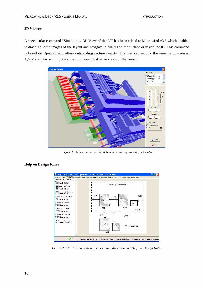
3D Viewer
A spectacular command “Simulate → 3D View of the IC” has been added to Microwind v3.5 which enables
to draw real-time images of the layout and navigate in fill-3D on the surface or inside the IC. This command
is based on OpenGL and offers outstanding picture quality. The user can modify the viewing position in
X,Y,Z and play with light sources to create illustrative views of the layout.
Figure 1: Access to real-time 3D-view of the layout using OpenGl
Help on Design Rules
Figure 2 : illustration of design rules using the command Help → Design Rules
MICROWIND & DSCH V3.5 - USER'S MANUAL INTRODUCTION
11
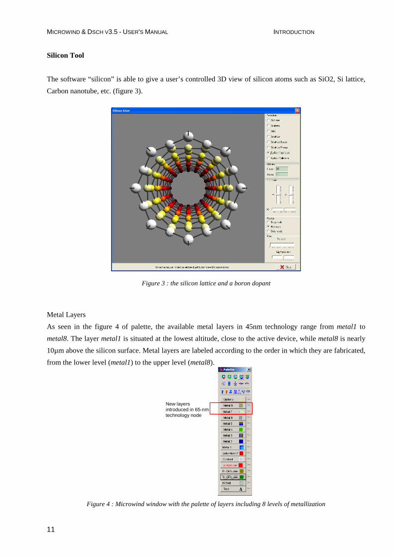
Silicon Tool
The software “silicon” is able to give a user’s controlled 3D view of silicon atoms such as SiO2, Si lattice,
Carbon nanotube, etc. (figure 3).
Figure 3 : the silicon lattice and a boron dopant
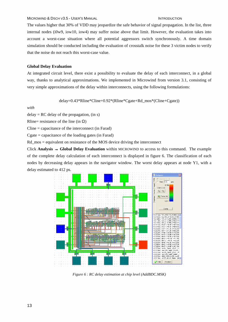
Metal Layers
As seen in the figure 4 of palette, the available metal layers in 45nm technology range from metal1 to
metal8. The layer metal1 is situated at the lowest altitude, close to the active device, while metal8 is nearly
10µm above the silicon surface. Metal layers are labeled according to the order in which they are fabricated,
from the lower level (metal1) to the upper level (metal8).
New layers introduced in 65-nm technology node
Figure 4 : Microwind window with the palette of layers including 8 levels of metallization

MICROWIND & DSCH V3.5 - USER'S MANUAL INTRODUCTION
12
In Microwind3.5, the macros which ease the addition of contacts in the layout have been updated to handle
up to 8 layers of metal.
Global Crosstalk Evaluation
An evaluation of the crosstalk effect based on analytical approximations of the coupling amplitude is
available using the command Analysis→→→→ Global Crosstalk analysis to access to this command. The
example of the complete crosstalk calculation of each interconnect for the layout “AddBCD.MSK” is
displayed in figure 5. The formulations used for the computation of the crosstalk voltage ∆V are shown
below.
victimx C
CC 12=
affector
affector
victim
victim
W
L
L
Wx =
xC
CVV
x
xdd ++
=∆1
1
1
With
C12 = crosstalk capacitance (Farad)
Cvictim = capacitance of victim
(Farad)
W = width of MOS device (m)
L = length of MOS device (m)
Vdd = supply voltage (V)
Caffector
Substrate (Ground)
Cvictim
C12
Figure 5: Global crosstalk extraction and classification of dangerous nodes (AddBCD.MSK)
In figure 5, the nodes in red correspond to the highest crosstalk noise, while the nodes in blue have almost
no noise due to lateral coupling. Vss and Vdd nodes may be removed from the list, and interconnects with
length less than a user’s defined value may also be removed.
MICROWIND & DSCH V3.5 - USER'S MANUAL INTRODUCTION
13
The values higher that 30% of VDD may jeopardize the safe behavior of signal propagation. In the list, three
internal nodes (i0w9, iow10, iow4) may suffer noise above that limit. However, the evaluation takes into
account a worst-case situation where all potential aggressors switch synchronously. A time domain
simulation should be conducted including the evaluation of crosstalk noise for these 3 victim nodes to verify
that the noise do not reach this worst-case value.
Global Delay Evaluation
At integrated circuit level, there exist a possibility to evaluate the delay of each interconnect, in a global
way, thanks to analytical approximations. We implemented in Microwind from version 3.1, consisting of
very simple approximations of the delay within interconnects, using the following formulations:
delay=0.43*Rline*Cline+0.92*(Rline*Cgate+Rd_mos*(Cline+Cgate))
with
delay = RC delay of the propagation, (in s)
Rline= resistance of the line (in Ω)
Cline = capacitance of the interconnect (in Farad)
Cgate = capacitance of the loading gates (in Farad)
Rd_mos = equivalent on resistance of the MOS device driving the interconnect
Click Analysis →→→→ Global Delay Evaluation within MICROWIND to access to this command. The example
of the complete delay calculation of each interconnect is displayed in figure 6. The classification of each
nodes by decreasing delay appears in the navigator window. The worst delay appears at node Y1, with a
delay estimated to 412 ps.
Figure 6 : RC delay estimation at chip level (AddBDC.MSK)

MICROWIND & DSCH V3.5 - USER'S MANUAL INTRODUCTION
14
Invert Diffusion N <-> P
This command is useful to invert the nature of the diffusion. All N+ diffusions included in the given are
become P+, and vice versa, as illustrated in figure 7.
Figure 7: inverting the nature of the diffusion
Label List
The most convenient way to find a text in the layout is to invoke View →→→→ Label List. The list of text labels
appears in the navigator menu. If you click on the desired text, the screen is redrawn so that the text label is
at the center of the window, with two lines drawing a cross at the text location. Its properties appear in the
navigator menu.
• Click on Hide to close the navigator window.
• Click on Extract to add the electrical properties of the selected text if the layout has not been
previously extracted.
In the case of a very long text list, select the first letter of the text at hand, press that letter on the keyboard.
This will automatically effect and alphabetic research and the selector will move to the first label starting
with the selected letter.
Mathematical Signal Description
A user’s defined equation may be entered to create virtually any type of waveform. Examples are given
below. The full list of functions is reported in table 1.

MICROWIND & DSCH V3.5 - USER'S MANUAL INTRODUCTION
15
Abs Absolute value
Arcos Invert cosine
Arcsin Invert sinus
Arctan Invert tangent
Abs Absolute value
Avg Average of the signal
Cos Cosine
CosH Hyperbolic Cosine
Exp Exponent
Gauss Gaussian noise; the parameter is the variance
Int Integral
Logic Random logic value between VDD and VSS, changed at period given as a
parameter.
Norm Normal distribution
Pi 3.1415927
P2 2*pi
Pos Positive value of the signal
RMS Root mean square
Sin Sinus
SinH Hyperbolic Sinus
Sqr Square
Sqrt Square root
White White noise; the parameter is the amplitude
t Time in seconds
TAN Tangent
VDD Voltage supply; given in the technology file
VDDH High Voltage supply; given in the technology file
x Time in seconds
Table 1: Functions provided in the MATH simulation property
Zoom In Navigator
The zoom navigator is now merged with palette for easy access for zoom functions.

MICROWIND & DSCH V3.5 - USER'S MANUAL INTRODUCTION
16
INSTALLATION
Connect to the web page www.microwind.net for the latest information about how to download the
lite version of the software. Once installed, two directories are created, one for MICROWIND35, one for
DSCH35, as illustrated below. C:\Program Files\Microwind
Microwind35 Dsch35
examples html
rules system
*.MSK Help files
*.RUL *.EXE
examples html
rules system
*.SCH Help files
*.TEC *.EXE
ieee
Symbol library (*.SYM)
Figure 0-1: The architecture of Microwind and Dsch
Once installed, two directories are created, one for MICROWIND35, one for DSCH35. In each directory, a
sub-directory called html contains help files. In MICROWIND35, other sub-directories include example files
(*.MSK), design rules (*.RUL) and system files (mainly microwind35.exe). In DSCH35, other sub-
directories include example files (*.SCH and *.SYM), design rules (*.TEC) and system files (mainly
dsch35.exe).

MICROWIND & DSCH V3.5 - USER'S MANUAL 1. TECHNOLOGY SCALE DOWN
17
The Moore’s Law
Recognizing a trend in integrated circuit complexity, Intel co-founder Gordon Moore extrapolated the
tendency and predicted an exponential growth in the available memory and calculation speed of
microprocessors which, he said in 1965, would double every year [Moore]. With a slight correction (i.e.
doubling every 18 months, see figure 1-1 ), Moore’s Law has held up to the Itanium® 2 processor which has
around 400 million transistors.
1970
1K
1 MEG
10 MEG
100 MEG
1 GIGA
Circuit Complexity
Year
8086
386TM
Moore’law with a doubling each year
Pentium ®
80286
1975 1980 1985 1990 1995 2000 2005 2010
10K
100K
4004 8008
8080
486TM Pentium II®
Pentium III®
Pentium 4 ®
8 bits
16 bits
32 bits
Itanium ® Moore’s law with a doubling each 18 months
Figure 1-1 : Moore’s law compared to Intel processor complexity from 1970 to 2010.
Scaling Benefits
The trend of CMOS technology improvement continues to be driven by the need to integrate more functions
within a given silicon area. Table 1 gives an overview of the key parameters for technological nodes from
180 nm, introduced in 1999, down to 22 nm, which is supposed to be in production around 2011.
Technology node 130 nm 90 nm 65 nm 45 nm 32 nm 22 nm First production 2001 2003 2005 2007 2009 2011 Effective gate length
70 nm 50 nm 35 nm 25 nm 17 nm 12 nm
Gate material Poly
Poly
Poly
Metal
Metal
Metal
Gate dielectric SiO2 SiO2 SiON High K High K High K Kgates/mm2 240 480 900 1500 2800 4500 Memory point (µ2) 2.4 1.3 0.6 0.3 0.15 0.08
Table 1: Technological evolution and forecast up to 2011
1 Technology Scale Down

MICROWIND & DSCH V3.5 - USER'S MANUAL 1. TECHNOLOGY SCALE DOWN
18
1995 2000 2005 2010 2015
0.1nm
1nm
10nm
Gate Dielectric Thickness (nm)
Year
0.25µm
0.18µm
0.13µm 90nm
65nm
32nm
High voltage MOS (double gate oxide)
Technology addressed in
Microwind 3.5
22nm
Low voltage MOS (minimum
gate oxide)
SiO2 (εr=3.9)
45nm
SiON (εr=4.2-6.5)
HighK (ε r=7-20)
Figure 1-2 : The technology scale down towards nano-scale devices
At each lithography scaling, the linear dimensions are approximately reduced by a factor of 0.7, and the
areas are reduced by factor of 2. Smaller cell sizes lead to higher integration density which has risen to
nearly 1.5 million gates per mm2 in 45 nm technology (table 1).
Gate Material and Oxide
For 40 years, the SiO2 gate oxide combined with polysilicon have been serving as the key enabling
materials for scaling MOS devices down to the 90nm technology node (Fig. 1). One of the struggles the IC
manufacturers went through was being able to scale the gate dielectric thickness to match continuous
requirements for improved switching performance. The thinner the gate oxide, the higher the transistor
current and consequently the switching speed. However, thinner gate oxide also means more leakage
current. Starting with the 90nm technology, SiO2 has been replaced by SiON dielectric, which features a
higher permittivity and consequently improves the device performances while keeping the parasitic leakage
current within reasonable limits. Starting with the 45-nm technology, leakage reduction has been achieved
through the use of various high-K dielectrics such as Hafnium Oxide HfO2 (εr=12), Zyrconium Oxide ZrO2
(εr=20), Tantalum Oxide Ta2O5 (εr=25) or Titanium Oxide TiO2 (εr=40). This provides much higher device
performance as if the device was fabricated in a technology using conventional SiO2 with much reduced
“equivalent SiO2 thickness”.
For the first time in 40 years of CMOS manufacturing, the poly gate has been abandoned. Nickel-Silicide
(NiSi), Titanium-Nitride (TiN) etc. are the types of gate materials that provide acceptable threshold voltage
and alleviate the mobility degradation problem (Fig. 3). In combination with Hafnium Oxide (HfO2, εr=12),
the metal/high-k transistors feature outstanding current switching capabilities together with low leakage.
Increased on current, decreased off current and significantly decreased gate leakage are obtained with this
novel combination. The sheet resistance is around 5Ω/square for the metal gate.

MICROWIND & DSCH V3.5 - USER'S MANUAL 1. TECHNOLOGY SCALE DOWN
19
1.2nm K=3.9
Source
Polysilicon gate
Si02 Gate oxide
Drain
2.0 nm K=12.0
Source
Novel METAL gate (Nickel
Silicide) Hafnium Gate oxide
Drain
Low capacitance (slow device)
High gate leakage 90-nm generation
Equivalent to 0.6 nm SiO2, which means a higher capacitance
(fast device) Reduced gate leakage
Low resistive layer (SiN)
Low resistive layer (SiN)
Figure 1-3 : The metal gate combined with High-K oxide material enhance the MOS device performance in terms of
switching speed and significantly reduce the leakage
10-10
10-9
10-8
10-7
10-6
10-5
10-4
10-3
0.0 0.5 1.0
Poly - SiO2
High-κ
Gate voltage (V)
Drain current (A/µm)
Ioff current decrease
Ion current increase
100
150
200
250
0.0 1.0 2.0
Optimized TiN/HfO2
Equivalent Gate Oxide (nm)
Effective Electron mobility (cm2/V.s)
Poly/HfO2
@ 1 MV/cm
Poly/SiO2
Figure 1-4 : The metal gate combined with High-K oxide material enhances the Ion current and drastically reduces the
Ioff current (left). Electron mobility vs. Equivalent gate oxide thickness for various materials (right).
The effective electron mobility is significantly reduced with a decrease of the equivalent gate oxide
thickness, as seen in Fig. 1-4, which compiles information from [Chau2004] [Lee2005][Song2006]. It can
be seen that the highest mobility is obtained with optimized TiN/HfO2, while Poly/ HfO2 do not lead to
suitable performances.
Strained Silicon
Strained silicon has been introduced starting with the 90-nm technology [Sicard2005b], [Sicard2006b] to
speed-up the carrier mobility, which boosts both the n-channel and p-channel transistor performances.
PMOS transistor channel strain has been enhanced by increasing the Germanium (Ge) content in the
compressive SiGe (silicium-germanium) film. Both transistors employ ultra shallow source-drains to further
increase the drive currents.

MICROWIND & DSCH V3.5 - USER'S MANUAL 1. TECHNOLOGY SCALE DOWN
20
Electron movement is slow as the distance between Si atoms is small
Electron movement is faster as the distance between Si atoms is increased
Source (Si)
Gate
Gate oxide
Horizontal strain created by the silicon nitride capping layer
Drain (Si)
Drain (Si) Source
(Si)
Figure 1-5 : Tensile strain generated by a silicon-nitride capping layer which increases the distance between atoms
underneath the gate, which speeds up the electron mobility of n-channel MOS devices
Hole movement is slow as the distance between Si atoms is large
Hole movement is faster as the horizontal distance between Si atoms is reduced
SiGe Si Si SiGe
Gate
Gate oxide
Horizontal pressure created by the uniaxial SiGe strain
Figure 1-6 : Compressive strain to reduce the distance between atoms underneath the gate, which speeds up the hole
mobility of p-channel MOS devices
Let us assume that the silicon atoms form a regular lattice structure, inside which the carriers participating
to the device current have to flow. In the case of electron carriers, stretching the lattice (by applying tensile
strain) allows the electrons to flow faster from the source to the drain, as depicted in Fig. 1-5. The mobility
improvement exhibits a linear dependence on the tensile film thickness. In a similar way, compressing the
lattice slightly speeds up the p-type transistor, for which current carriers consist of holes (Fig. 1-6). The
combination of reduced channel length, decreased oxide thickness and strained silicon achieves a substantial
gain in drive current for both nMOS and pMOS devices.
Market
The integrated circuit market has been growing steadily since many years, due to ever-increasing demand
for electronic devices. The production of integrated circuits for various technologies over the years is
illustrated in Fig. 1-7. It can be seen that a new technology has appeared regularly every two years, with a
ramp up close to three years. The production peak is constantly increased, and similar trends should be
observed for novel technologies such as 45nm (forecast peak in 2010).

MICROWIND & DSCH V3.5 - USER'S MANUAL 1. TECHNOLOGY SCALE DOWN
21
1995 2000 2005 2010 2015
Production
Year
0. 5µm
0.18µm
130nm
90nm
45nm
0.35µm
0.25µm
32nm
65nm
Figure 1-7 : Technology ramping every two years introducing the 45 nm technology
Prototype 45-nm processes have been introduced by TSMC in 2004 [Tsmc2004] and Fujitsu in 2005
[Fujitsu2005]. In 2007, Intel announced its 45-nm CMOS industrial process and revealed some key features
about metal gates. The “Common Platform” [Common2007] including IBM, Chartered Semiconductor, The
transistor channels range from 25 nm to 40 nm in size (25 to 40 billionths of a meter). Some of the key
features of the 45 nm technologies from various providers are given in Table 2.
Parameter Value VDD (V) 0.85-1.2 V Effective gate length (nm) 25-40 Ion N (µA/µm) at 1V 750-1000 Ion P (µA/µm) at 1V 350-530 Ioff N (nA/µm) 5-100 Ioff P (nA/µm) 5-100 Gate dielectric SiON, HfO2, ZrO2, Ta2O5, TiO2 Equivalent oxide thickness (nm)
1.1-1.5
# of metal layers 6-10 Interconnect layer permittivity K
2.2-2.6
Table 2: Key features of the 45 nm technology
Compared to 65-nm technology, most 45-nm technologies offer:
- 30 % increase in switching performance
- 30 % less power consumption
- 2 times higher density
- X 2 reduction of the leakage between source and drain and through the gate oxide
45-nm process variants

MICROWIND & DSCH V3.5 - USER'S MANUAL 1. TECHNOLOGY SCALE DOWN
22
There may exist several variants of the 45-nm process technology. One corresponds to the highest possible
speed, at the price of a very high leakage current. This technology is called “High speed” as it is dedicated
to applications for which the highest speed is the primary objective: fast microprocessors, fast DSP, etc.
Parasitic
leakage current
High (x 10)
Moderate (x 1)
Low (x 0.1)
Speed
Fast (+50%)
Moderate (0%)
Low (-50%)
High-end servers
Servers
Networking
Computing
Mobile Computing
Consumer
3G phones
2G phones
MP3
Digital camera
High speed variant
General Purpose variant
Low leakage variant
Microwind 45-nm rule file
Personal org.
Figure 1-8 : Introducing three variants of the 45-nm technology
This technology has not been addressed in Microwind’s 45nm rule file. The second technological option
called “General Purpose” (Fig. 1-8) is targeted to standard products where the speed factor is not critical.
The leakage current is one order of magnitude lower than for the high-speed variant, with gate switching
decreased by 50%. Only this technology has been implemented in Microwind [Sicard2007].
There may also exist a third variant called low leakage (bottom left of Fig. 1-8). This variant concerns
integrated circuits for which the leakage current must remain as low as possible, a criterion that ranks first
in applications such as embedded devices, mobile phones or personal organizers. The operational voltage is
usually from 0.8 V to 1.2 V, depending on the technology variant. In Microwind, we decided to fix VDD at
1.0 V in the cmos45nm.RUL rule file, which represents a compromise between all possible technology
variations available for this 45-nm node [Sicard2007].
In 2010, Microwind 3.5 has also been tuned to the 32-nm node [Sicard2010], with the introduction of
Ion/Ioff trends and process variability, as described in Fig. 1-9. Further improvements have been achieved
for unmatched MOS performances (very high Ion, reasonable Ioff).
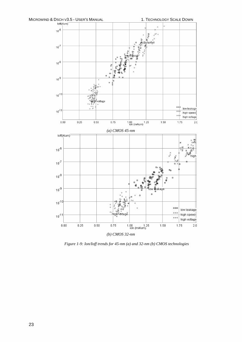
MICROWIND & DSCH V3.5 - USER'S MANUAL 1. TECHNOLOGY SCALE DOWN
23
(a) CMOS 45-nm
(b) CMOS 32-nm
Figure 1-9: Ion/Ioff trends for 45-nm (a) and 32-nm (b) CMOS technologies

MICROWIND & DSCH V3.5 - USER'S MANUAL 2. The MOS device
24
This chapter presents the CMOS transistor, its layout, static characteristics and dynamic characteristics. The
vertical aspect of the device and the three dimensional sketch of the fabrication are also described.
Logic Levels
Three logic levels 0,1 and X are defined as follows:
Logical value Voltage Name Symbol in DSCH Symbol in MICROWIND 0 0.0V VSS
(Green in logic simulation)
(Green in analog simulation)
1 1.0V in cmos 65nm
VDD
(Red in logic simulation)
(Red in analog simulation)
X Undefined X (Gray in simulation) (Gray in simulation)
The MOS as a switch
The MOS transistor is basically a switch. When used in logic cell design, it can be on or off. When on, a
current can flow between drain and source. When off, no current flow between drain and source. The MOS
is turned on or off depending on the gate voltage. In CMOS technology, both n-channel (or nMOS) and p-
channel MOS (or pMOS) devices exist. The nMOS and pMOS symbols are reported below. The symbols
for the ground voltage source (0 or VSS) and the supply (1 or VDD) are also reported in figure 2-1.
The n-channel MOS device requires a logic value 1 (or a supply VDD) to be on. In contrary, the p-channel
MOS device requires a logic value 0 to be on. When the MSO device is on, the link between the source and
drain is equivalent to a resistance. The order of range of this ‘on’ resistance is 100 Ω-5 KΩ. The ‘off’
resistance is considered infinite at first order, as its value is several Mega-Ω.
0 1
0 1
Figure 2-1 : the MOS symbol and switch
2 The MOS device

MICROWIND & DSCH V3.5 - USER'S MANUAL 2. The MOS device
25
MOS layout
We use MICROWIND to draw the MOS layout and simulate its behavior. Go to the directory in which the
software has been copied (By default Microwind35 ). Double-click on the MICROWIND icon.
The MICROWIND display window includes four main windows: the main menu, the layout display window,
the icon menu and the layer palette. The layout window features a grid, scaled in lambda (λ) units. The
lambda unit is fixed to half of the minimum available lithography of the technology. The default technology
is a CMOS 8-metal layers 45 nm technology. In this technology, lambda is 0.02 µm (40 nm).
Figure 2-2 :The MICROWIND window as it appears at the initialization stage..
The palette is located in the lower right corner of the screen. A red color indicates the current layer. Initially
the selected layer in the palette is polysilicon. By using the following procedure, you can create a manual
design of the n-channel MOS.
Fix the first corner of the box with the mouse. While keeping the mouse button pressed, move the
mouse to the opposite corner of the box. Release the button. This creates a box in polysilicon layer as
shown in Figure 2-3. The box width should not be inferior to 2 λ, which is the minimum width of the
polysilicon box.
Change the current layer into N+ diffusion by a click on the palette of the Diffusion N+ button. Make
sure that the red layer is now the N+ Diffusion. Draw a n-diffusion box at the bottom of the drawing
as in Figure 2-3. N-diffusion boxes are represented in green. The intersection between diffusion and
polysilicon creates the channel of the nMOS device.

MICROWIND & DSCH V3.5 - USER'S MANUAL 2. The MOS device
26
Figure 2-3 : Creating the N-channel MOS transistor
Vertical aspect of the MOS
Click on this icon to access process simulation (Command Simulate →→→→ Process section in 2D). The cross-
section is given by a click of the mouse at the first point and the release of the mouse at the second point. In
the example of Figure 2-4, three nodes appear in the cross-section of the n-channel MOS device: the gate
(red), the left diffusion called source (green) and the right diffusion called drain (green), over a substrate
(gray). A thin oxide called the gate oxide isolates the gate. Various steps of oxidation have lead to stacked
oxides on the top of the gate.
NMOS drain (N+ doped)
Compressive strain around the NMOS gate
MOS gate (TiN)
Inter-layer oxide (low permittivity)
field oxide (SiO2)
NMOS source (N+ doped)
Shallow trench isolation (STI, built in (SiO2)
Silicon substrate (lightly doped P)
Figure 2-4 : The cross-section of the nMOS devices.
MICROWIND & DSCH V3.5 - USER'S MANUAL 2. The MOS device
27
The physical properties of the source and of the drain are exactly the same. Theoretically, the source is the
origin of channel impurities. In the case of this nMOS device, the channel impurities are the electrons.
Therefore, the source is the diffusion area with the lowest voltage. The metal gate floats over the channel,
and splits the diffusion into 2 zones, the source and the drain. The gate controls the current flow from the
drain to the source, both ways. A high voltage on the gate attracts electrons below the gate, creates an
electron channel and enables current to flow. A low voltage disables the channel.
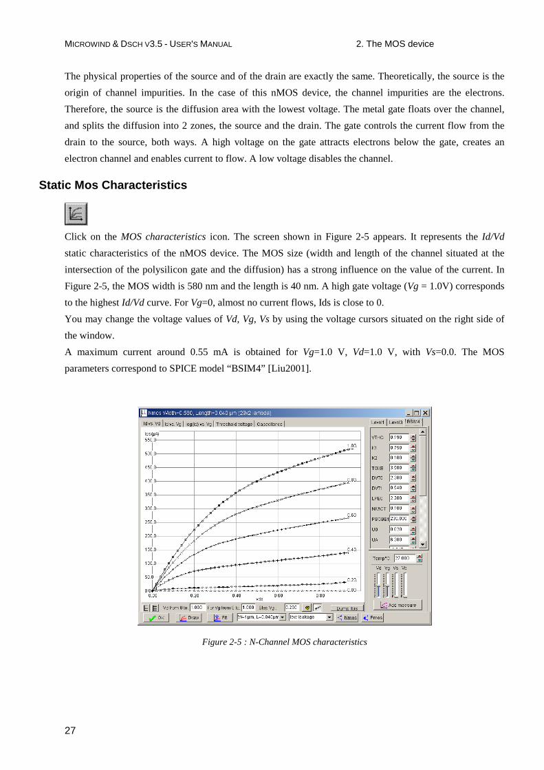
Static Mos Characteristics
Click on the MOS characteristics icon. The screen shown in Figure 2-5 appears. It represents the Id/Vd
static characteristics of the nMOS device. The MOS size (width and length of the channel situated at the
intersection of the polysilicon gate and the diffusion) has a strong influence on the value of the current. In
Figure 2-5, the MOS width is 580 nm and the length is 40 nm. A high gate voltage (Vg = 1.0V) corresponds
to the highest Id/Vd curve. For Vg=0, almost no current flows, Ids is close to 0.
You may change the voltage values of Vd, Vg, Vs by using the voltage cursors situated on the right side of
the window.
A maximum current around 0.55 mA is obtained for Vg=1.0 V, Vd=1.0 V, with Vs=0.0. The MOS
parameters correspond to SPICE model “BSIM4” [Liu2001].
Figure 2-5 : N-Channel MOS characteristics

MICROWIND & DSCH V3.5 - USER'S MANUAL 2. The MOS device
28
Dynamic MOS behavior
This paragraph concerns the dynamic simulation of the MOS to exhibit its switching properties. The most
convenient way to operate the MOS is to apply a clock to the gate, another to the source and to observe the
drain. The summary of available properties that can be added to the layout is reported below.
VDD property
VSS property
Clock property Pulse property
Node visible
Sinusoidal wave
High voltage property
Apply a clock to the gate. Click on the Clock icon and then, click on the polysilicon gate. The
clock menu appears again. Change the name into Vgate and click on OK to apply a clock with
0.1 ns period (45 ps at “0”, 5 ps rise, 45 ps at “1”, 5 ps fall).
Figure 2-6 : The clock menu and the clock property insertion directly on the MOS layout
Apply a clock to the drain. Click on the Clock icon, click on the left diffusion. The Clock menu
appears. Change the name into Vdrain and click on OK . A default clock with 0.2 ns period is
generated. The Clock property is sent to the node and appears at the right hand side of the desired
location with the name Vdrain .
MICROWIND & DSCH V3.5 - USER'S MANUAL 2. The MOS device
29
Watch the output: Click on the Visible icon and then, click on the right diffusion. Click OK . The
Visible property is then sent to the node. The associated text s1 is in italic, meaning that the
waveform of this node will appear at the next simulation.
Always save BEFORE any simulation. The analog simulation algorithm may cause run-time errors leading
to a loss of layout information. Click on File → Save as. A new window appears, into which you enter the
design name. Type for example Mosn.MSK. Then click on Save. The design is saved under that filename.
Analog Simulation
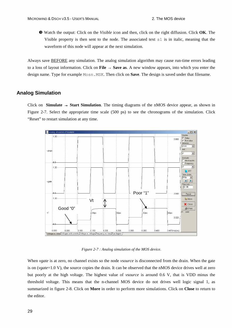
Click on Simulate →→→→ Start Simulation. The timing diagrams of the nMOS device appear, as shown in
Figure 2-7. Select the appropriate time scale (500 ps) to see the chronograms of the simulation. Click
“Reset” to restart simulation at any time.
Vt
Good “0”
Poor “1”
Figure 2-7 : Analog simulation of the MOS device.
When vgate is at zero, no channel exists so the node vsource is disconnected from the drain. When the gate
is on (vgate=1.0 V), the source copies the drain. It can be observed that the nMOS device drives well at zero
but poorly at the high voltage. The highest value of vsource is around 0.6 V, that is VDD minus the
threshold voltage. This means that the n-channel MOS device do not drives well logic signal 1, as
summarized in figure 2-8. Click on More in order to perform more simulations. Click on Close to return to
the editor.

MICROWIND & DSCH V3.5 - USER'S MANUAL 2. The MOS device
30
1 0
1
0 Good 0
1
1 Poor 1 (VDD-Vt)
Figure 2-8 : The nMOS device behavior summary
The MOS Models
Mos Level 1
For the evaluation of the current Ids between the drain and the source as a function of Vd,Vg and Vs, you
may use the old but nevertheless simple LEVEL1 described below. The parameters listed in table 2-1
correspond to “low leakage” MOS option, which is the default MOS option in 45 nm technology. When
dealing with sub-micron technology, the model LEVEL1 is more than 4 times too optimistic regarding
current prediction, compared to real-case measurements.
ε0 = 8.85 10-12 F/m is the absolute permittivity
εr = relative permittivity, equal to 10 in the case of HfO2 (no unit)
Mode Condition Expression for the current Ids CUT-OFF Vgs<0 0 Ids= LINEAR Vds<Vgs-Vt
))2
)(Vvt).V((V
εε Ids
2ds
dsgsr0 −−=
L
W.
TOXUO
SATURATED Vds>Vgs-Vt 2
gsr0 vt)(Vεε
Ids −=L
W.
TOXUO
Mos Level1 parameters Parameter Definition Typical Value 45nm NMOS PMOS VTO Threshold voltage 0.18 V -0.15 V U0 Carrier mobility 0.016 m2/V-s 0.012 m2/V-s TOXE Equivalent gate oxide thickness 3.5 nm 3.5 nm PHI Surface potential at strong
inversion 0.15 V 0.15 V
GAMMA Bulk threshold parameter 0.4 V0.5 0.4 V0.5 W MOS channel width 80 nm minimum 80 nm minimum L MOS channel length 40 nm minimum 40 nm minimum
Table 2-1: Parameters of MOS level 1 implemented into Microwind
The High-K dielectric enabled a thinner “equivalent” oxide thickness while keeping leakage current low.
The “equivalent oxide thickness” TOXE is defined by Equ. 1. For the 45-nm technology, the high-K
MICROWIND & DSCH V3.5 - USER'S MANUAL 2. The MOS device
31
permittivity declared in the rule file is 10 (Parameter “GateK”), close to HfO2 gate dielectric permittivity.
The physical oxide thickness is 3.5 nm, and by applying equ. 1, TOXE is 1.4nm. These parameters are in
close agreement with those in Song’s review on 45-nm gate stacks [Song2006].
= −
−khigh
khigh
SiO tTOXEεε 2 (Equ. 1)
Where
εSiO2 = dielectric permittivity of SiO2 (3.9, no unit)
εhigh-k = High-K dielectric permittivity
thigh-k = High-K oxide thickness (m)
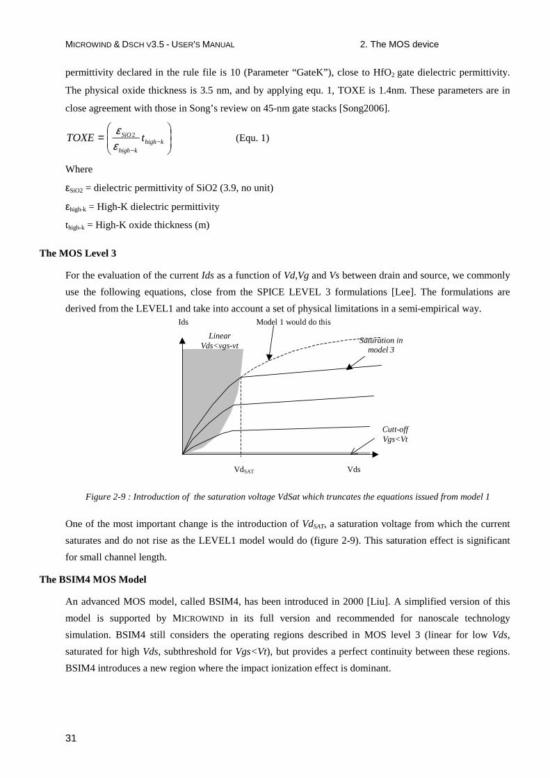
The MOS Level 3
For the evaluation of the current Ids as a function of Vd,Vg and Vs between drain and source, we commonly
use the following equations, close from the SPICE LEVEL 3 formulations [Lee]. The formulations are
derived from the LEVEL1 and take into account a set of physical limitations in a semi-empirical way.
Vds
Ids
LinearVds<vgs-vt
Saturation inmodel 3
Model 1 would do this
Cutt-offVgs<Vt
VdSAT
Figure 2-9 : Introduction of the saturation voltage VdSat which truncates the equations issued from model 1
One of the most important change is the introduction of VdSAT, a saturation voltage from which the current
saturates and do not rise as the LEVEL1 model would do (figure 2-9). This saturation effect is significant
for small channel length.
The BSIM4 MOS Model
An advanced MOS model, called BSIM4, has been introduced in 2000 [Liu]. A simplified version of this
model is supported by MICROWIND in its full version and recommended for nanoscale technology
simulation. BSIM4 still considers the operating regions described in MOS level 3 (linear for low Vds,
saturated for high Vds, subthreshold for Vgs<Vt), but provides a perfect continuity between these regions.
BSIM4 introduces a new region where the impact ionization effect is dominant.

MICROWIND & DSCH V3.5 - USER'S MANUAL 2. The MOS device
32
The number of parameters specified in the official release of BSIM4 is as high as 300. A significant portion
of these parameters is unused in our implementation. We concentrate on the most significant parameters, for
educational purpose. The set of parameters is reduced to around 20, shown in the right part of figure 2-10.
Figure 2-10 : Implementation of BSIM4 within Microwind (full version only)
The PMOS Transistor
The p-channel transistor simulation features the same functions as the n-channel device, but with opposite
voltage control of the gate. For the nMOS, the channel is created with a logic 1 on the gate. For the pMOS,
the channel is created for a logic 0 on the gate. Load the file pmos.msk and click the icon MOS
characteristics. The p-channel MOS simulation appears, as shown in Figure 2-11.

MICROWIND & DSCH V3.5 - USER'S MANUAL 2. The MOS device
33
Figure 2-11 : Layout and simulation of the p-channel MOS (mypmos.MSK)
Note that the pMOS gives approximately half of the maximum current given by the nMOS with the same
device size. The highest current is obtained with the lowest possible gate voltage, that is 0. From the
simulation of figure 2-11, we see that the pMOS device is able to pass well the logic level 1. But the logic
level 0 is transformed into a positive voltage, equal to the threshold voltage of the MOS device (0.35 V).
The summary of the p-channel MOS performances is reported in figure 2-12.
0 1
0
0 Poor 0 (0+Vt)
0
1 Good 1
PMOS
Figure 2-12 : Summary of the performances of a pMOS device
MOS device options
The default MOS device in Microwind 3.5 is the “low leakage MOS”. There exist a possibility to use a
second type of MOS device called “High-speed”. The device I/V characteristics of the low-leakage and
high-speed MOS devices listed in Table 3 are obtained using the MOS model BSIM4 (See [Sicard2005a]
for more information about this model). The cross-section of the low-leakage and high-speed MOS devices
do not reveal any major difference (Fig. 2-13), except a reduction of the effective channel length.
Concerning the low-leakage MOS, the I/V characteristics reported in Fig. 2-14 demonstrate a drive current

MICROWIND & DSCH V3.5 - USER'S MANUAL 2. The MOS device
34
capability of around 0.9 mA/µm for W=1.0µm at a voltage supply of 1.0 V. For the high speed MOS, the
effective channel length is slightly reduced as well as the threshold voltage, to achieve an increased drive
current of around 1.2 mA/µm.
nMOS gate
Contact to metal1
Metal1 layer
Shallow trench isolation (STI)
35 nm effective channel 30 nm effective
channel
Low leakage nMOS
High speed nMOS
High stress film to induce channel strain
High-k oxide and TiN gate
Figure 2-13 : Cross-section of the nMOS devices (allMosDevices.MSK)
Parameter NMOS Low leakage
NMOS High speed
Drawn length (nm) 40 40 Effective length (nm) 35 30 Threshold voltage (V) 0.20 0.18 Ion (mA/µm) at VDD=1.0V 0.9 1.2 Ioff (nA/µm) 7 200
Table 3: nMOS parameters featured in the CMOS 45-nm technology provided in Microwind

MICROWIND & DSCH V3.5 - USER'S MANUAL 2. The MOS device
35
Imax=0.9 mA
25% increase of the maximum current
Low-leakage Ion
High-speed Ion
(a) Low leakage W=1µm, Leff= 35nm (b) High speed W=1µm, Leff= 30nm
Figure 2-14 : Id/Vd characteristics of the low leakage and high speed nMOS devices
Id/Vg for Vb=0, Vds=1 V
Ioff=7 nA
Vt=0.2 V
Ioff=200 nA
Vt=0.2 V
(a) low leakage MOS (Leff=35 nm) (b) high speed MOS (W=1 µm, Leff=30 nm)
Figure 2-15 : Id/Vg characteristics (log scale) of the low leakage and high-speed nMOS devices
The drawback of the high-speed MOS current drive is the leakage current which rises from 7 nA/µm (low
leakage) to 200 nA/µm (high speed), as seen in the Id/Vg curve at the X axis location corresponding to Vg=
0 V (Fig. 2-15 b).
High-Voltage MOS
At least three types of MOS devices exist within the 45-nm technology implemented in Microwind : the
low-leakage MOS (default MOS device), the high-speed MOS (higher switching performance but higher
leakage) and the high voltage MOS used for input/output interfacing. In Microwind’s cmos45nm rule file,
the I/O supply is 1.8 V. Most foundries also propose 2.5 V and 3.3 V interfacing.

MICROWIND & DSCH V3.5 - USER'S MANUAL 2. The MOS device
36
(1) Double click in the option box
(2) Modify the MOS option as « low leakage »
Figure 2-16 : Changing the MOS type through the option layer
The MOS type is changed using an option layer, situated at the upper part of the palette. The option layer
box should completely surround the MOS device layout. Double click the option layer. The Navigator menu
is set to the “Options” menu (Fig. 2-16). The default MOS type corresponds to the option “low leakage”
(Fig. 2-16). Change the option to “High Speed” and lauch the simulation again.
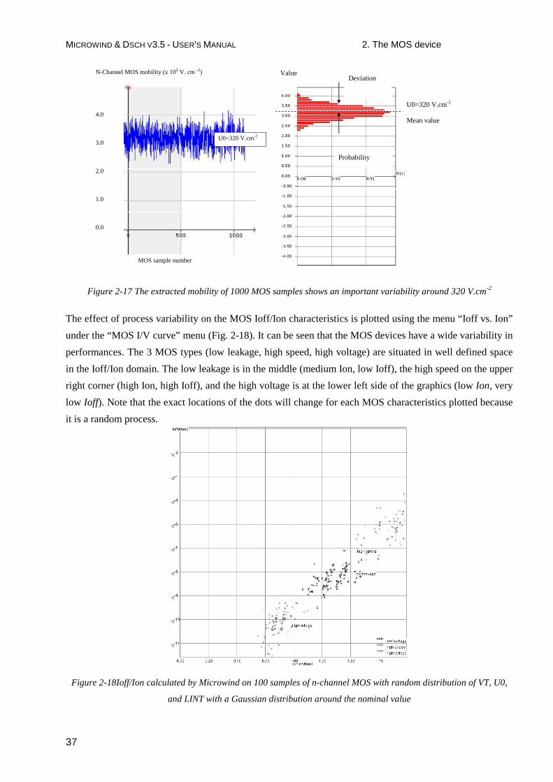
MOS Variability
One important challenge in nano-CMOS technology is process variability. The fabrication of millions of
MOS devices at nano-scale induces a spreading in switching performances in the same IC. The most
important parameters affected by process variability are the threshold voltage, the carrier mobility and the
effective channel length. Variations are handled in Microwind using random values in a Gaussian
distribution, which is expressed by the formulation of Equ. 2. An illustration of the variation in electron
mobility (parameter U0) for nearly a thousand MOS device samples is reported in Fig. 2-17.
2
2
2
)(
2
1 σ
σπ
mx
ef−−
= (Equ. 2)
where
f = probability density of the random variable (x axis in Fig.)
x = variable (y axis in Fig. 11)
σ = deviation
m = mean value
MICROWIND & DSCH V3.5 - USER'S MANUAL 2. The MOS device
37
3.0
2.0
1.0
0.0
4.0
N-Channel MOS mobility (x 102 V. cm -2)
MOS sample number
U0=320 V.cm-2
Probability
Value Deviation
Mean value
U0=320 V.cm-2
Figure 2-17 The extracted mobility of 1000 MOS samples shows an important variability around 320 V.cm-2
The effect of process variability on the MOS Ioff/Ion characteristics is plotted using the menu “Ioff vs. Ion”
under the “MOS I/V curve” menu (Fig. 2-18). It can be seen that the MOS devices have a wide variability in
performances. The 3 MOS types (low leakage, high speed, high voltage) are situated in well defined space
in the Ioff/Ion domain. The low leakage is in the middle (medium Ion, low Ioff), the high speed on the upper
right corner (high Ion, high Ioff), and the high voltage is at the lower left side of the graphics (low Ion, very
low Ioff). Note that the exact locations of the dots will change for each MOS characteristics plotted because
it is a random process.
Figure 2-18Ioff/Ion calculated by Microwind on 100 samples of n-channel MOS with random distribution of VT, U0,
and LINT with a Gaussian distribution around the nominal value

MICROWIND & DSCH V3.5 - USER'S MANUAL 2. The MOS device
38
Very high Ion current
Very low Ion current
Very high Ioff current
Very low Ioff current
Average Ion current
Average Ioff current
Average trend in this 32-nm technology
High speed
Low leakage
Figure 2-19 Finding compromises between high current drive and high leakage current
Concerning “worst case” and “best case”, notice that
• Slow devices have high VT, low mobility U0 and long channel (LINT>0)
• Fast devices have low VT, high mobility U0, and short channel (LINT<0)
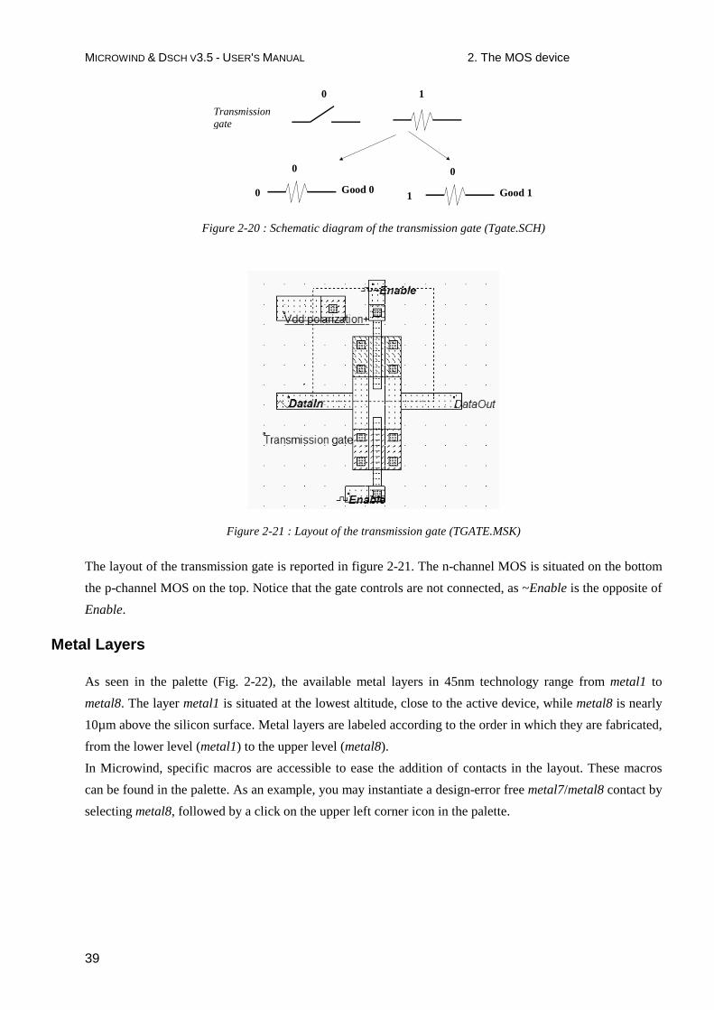
The Transmission Gate
Both NMOS devices and PMOS devices exhibit poor performances when transmitting one particular logic
information. The nMOS degrades the logic level 1, the pMOS degrades the logic level 0. Thus, a perfect
pass gate can be constructed from the combination of nMOS and pMOS devices working in a
complementary way, leading to improved switching performances. Such a circuit, presented in figure 2-20,
is called the transmission gate. In DSCH , the symbol may be found in the Advance menu in the palette. The
transmission gate includes one inverter, one nMOS and one pMOS.
MICROWIND & DSCH V3.5 - USER'S MANUAL 2. The MOS device
39
0 1
Transmission gate
0
0 Good 0
0
1 Good 1
Figure 2-20 : Schematic diagram of the transmission gate (Tgate.SCH)
Figure 2-21 : Layout of the transmission gate (TGATE.MSK)
The layout of the transmission gate is reported in figure 2-21. The n-channel MOS is situated on the bottom
the p-channel MOS on the top. Notice that the gate controls are not connected, as ~Enable is the opposite of
Enable.
Metal Layers
As seen in the palette (Fig. 2-22), the available metal layers in 45nm technology range from metal1 to
metal8. The layer metal1 is situated at the lowest altitude, close to the active device, while metal8 is nearly
10µm above the silicon surface. Metal layers are labeled according to the order in which they are fabricated,
from the lower level (metal1) to the upper level (metal8).
In Microwind, specific macros are accessible to ease the addition of contacts in the layout. These macros
can be found in the palette. As an example, you may instantiate a design-error free metal7/metal8 contact by
selecting metal8, followed by a click on the upper left corner icon in the palette.

MICROWIND & DSCH V3.5 - USER'S MANUAL 2. The MOS device
40
Metal layers used for short-distance interconnects
Layer used to connect metal to TinN, metal to N+, metal to P+
Figure 2-22 : Microwind window with the palette of layers including 8 levels of metallization
+ +
Metal1/Metal2 contact macro Metal1 Metal2 Via
Figure 2-23 : Access to contact macros between metal layers

MICROWIND & DSCH V3.5 - USER'S MANUAL 2. The MOS device
41
Contact poly/metal1..metal3
Contact poly-metal1-..-metal8
Contact P+diff/metal1..metal5
Contact Metal5..metal8
Figure 2-24: Examples of layer connection using the complex contact command from Microwind (Contacts.MSK)
A metal1/metal8 contact is depicted in Fig. 2-23. Additionally, access to complex stacked contacts is
proposed thanks to the icon "complex contacts" situated in the palette, in the second column of the second
row. The screen shown in Fig. 2-23 appears when you click on this icon. By default it creates a contact from
poly to metal1, and from metal1 to metal2. Tick more boxes “between metals” to build more complex
stacked contacts, as illustrated in the 2D cross-section reported in Fig. 2-24.
Each layer is embedded into a low dielectric oxide (referred to as “interconnect layer permittivity K” in
Table 2), which isolates the layers from each other. A cross-section of a 45-nm CMOS technology is shown
in Fig. 2-24. In 45-nm technology, the layers metal1..metal4 have almost identical characteristics.
Concerning the design rules, the minimum width w of the interconnect is 3 λ. The minimum spacing is 4 λ.
Layers metal5 and metal6 are a little thicker and wider, while layers metal7 and metal8 are significantly
thicker and wider, to drive high currents for power supplies. The design rules for metal8 are 25 λ (0.5µm)
width, 25 λ (0.5µm) spacing.
Added Features in the full version
BSIM4 The state-of-the art MOS model for accurate simulation of nano-scale technologies, including a tutorial on key parameters of the model.
High Speed Mos New kinds of MOS device has been introduced in deep submicron technologies, starting the 0.18µm CMOS process generation. The MOS called high speed MOS (HS) is available as well as the normal one, recalled Low leakage MOS (LL).
High Voltage MOS For I/Os operating at high voltage, specific MOS devices called "High voltage MOS" are used. The high voltage MOS is built using a thick oxide, two to three times thicker than the low voltage MOS, to handle high voltages as required by the I/O interfaces..
Temperature Effects Three main parameters are concerned by the sensitivity to temperature: the threshold voltage VTO, the mobility U0 and the slope in sub-threshold mode. The modeling of the temperature effect is described and illustrated .

MICROWIND & DSCH V3.5 - USER'S MANUAL 2. The MOS device
42
Process Variations Due to unavoidable process variations during the hundreds of chemical steps for the fabrication of the integrated circuit, the MOS characteristics are never exactly identical from one device to another, and from one die to an other. Monte-carlo simulation, min/max/typ simulations are provided in the full version.
Ion/Ioff trends The screen "Ion vs. Ioff" enables to see the ION/IOFF trends for a set of MOS devices with random distribution of VT, U0 and LEFF as detailed in the Process Variations menu. The three types of MOS devices (high speed, low leakage, high voltage) are displayed.

MICROWIND & DSCH V3.5 - USER'S MANUAL 3. The Inverter
43
This chapter describes the CMOS inverter at logic level, using the logic editor and simulator DSCH , and at
layout level, using the tool MICROWIND .
The Logic Inverter
In this section, an inverter circuit is loaded and simulated. Click File→→→→ Open in the main menu. Select
INV.SCH in the list. In this circuit are one button situated on the left side of the design, the inverter and a
led. Click Simulate→→→→ Start simulation in the main menu.
Figure 3-1 : The schematic diagram including one single inverter (Inverter.SCH)
Now, click inside the buttons situated on the left part of the diagram. The result is displayed on the leds. The
red value indicates logic 1, the black value means a logic 0. Click the button Stop simulation shown in the
picture below. You are back to the editor.
Figure 3-2 : The button Stop Simulation
Click the chronogram icon to get access to the chronograms of the previous simulation (Figure 3-3). As
seen in the waveform, the value of the output is the logic opposite of that of the input.
Figure 3-3 : Chronograms of the inverter simulation (CmosInv.SCH)
3 The Inverter

MICROWIND & DSCH V3.5 - USER'S MANUAL 3. The Inverter
44
Double click on the INV symbol, the symbol properties window is activated. In this window appears the
VERILOG description (left side) and the list of pins (right side). A set of drawing options is also reported in
the same window. Notice the gate delay (3 pico-second in the 45-nm technology), the fanout that represents
the number of cells connected to the output pin (1 cell connected), and the wire delay due to this cell
connection (an extra 2 ps delay).
The CMOS inverter
The CMOS inverter design is detailed in the figure below. Here the p-channel MOS and the n-channel MOS
transistors function as switches. When the input signal is logic 0 (Figure 3-4 left), the nMOS is switched off
while PMOS passes VDD through the output. When the input signal is logic 1 (Figure 3-4 right), the pMOS
is switched off while the nMOS passes VSS to the output.
Figure 3-4 : The MOS Inverter (File CmosInv.sch)
The fanout corresponds to the number of gates connected to the inverter output. Physically, a large fanout
means a large number of connections, that is a large load capacitance. If we simulate an inverter loaded with
one single output, the switching delay is small. Now, if we load the inverter by several outputs, the delay
and the power consumption are increased. The power consumption linearly increases with the load
capacitance. This is mainly due to the current needed to charge and discharge that capacitance.
Manual Layout of the Inverter
In this paragraph, the procedure to create manually the layout of a CMOS inverter is described. Click the
icon MOS generator on the palette. The following window appears. By default the proposed length is the
minimum length available in the technology (2 lambda), and the width is 10 lambda. In 45-nm technology,
where lambda is 20 nm (0.02 µm), the corresponding size is 0.02 µm for the length and 0.04 µm for the
width. Simply click Generate Device, and click on the middle of the screen to fix the MOS device.
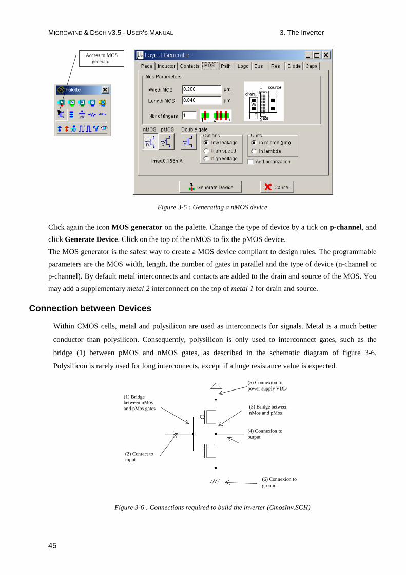
MICROWIND & DSCH V3.5 - USER'S MANUAL 3. The Inverter
45
Access to MOS generator
Figure 3-5 : Generating a nMOS device
Click again the icon MOS generator on the palette. Change the type of device by a tick on p-channel, and
click Generate Device. Click on the top of the nMOS to fix the pMOS device.
The MOS generator is the safest way to create a MOS device compliant to design rules. The programmable
parameters are the MOS width, length, the number of gates in parallel and the type of device (n-channel or
p-channel). By default metal interconnects and contacts are added to the drain and source of the MOS. You
may add a supplementary metal 2 interconnect on the top of metal 1 for drain and source.
Connection between Devices
Within CMOS cells, metal and polysilicon are used as interconnects for signals. Metal is a much better
conductor than polysilicon. Consequently, polysilicon is only used to interconnect gates, such as the
bridge (1) between pMOS and nMOS gates, as described in the schematic diagram of figure 3-6.
Polysilicon is rarely used for long interconnects, except if a huge resistance value is expected.
(1) Bridge between nMos and pMos gates
(2) Contact to input
(5) Connexion to power supply VDD
(6) Connexion to ground
(4) Connexion to output
(3) Bridge between nMos and pMos
Figure 3-6 : Connections required to build the inverter (CmosInv.SCH)
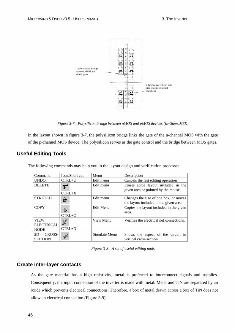
MICROWIND & DSCH V3.5 - USER'S MANUAL 3. The Inverter
46
(1) Polysilicon Bridge between pMOS and nMOS gates
2 lambda polysilicon gate size to achieve fastest switching
Figure 3-7 : Polysilicon bridge between nMOS and pMOS devices (InvSteps.MSK)
In the layout shown in figure 3-7, the polysilicon bridge links the gate of the n-channel MOS with the gate
of the p-channel MOS device. The polysilicon serves as the gate control and the bridge between MOS gates.
Useful Editing Tools
The following commands may help you in the layout design and verification processes.
Command Icon/Short cut Menu Description UNDO CTRL+U Edit menu Cancels the last editing operation DELETE
CTRL+X
Edit menu Erases some layout included in the given area or pointed by the mouse.
STRETCH
Edit menu Changes the size of one box, or moves the layout included in the given area.
COPY
CTRL+C
Edit Menu Copies the layout included in the given area.
VIEW ELECTRICAL NODE
CTRL+N
View Menu Verifies the electrical net connections.
2D CROSS-SECTION
Simulate Menu Shows the aspect of the circuit in vertical cross-section.
Figure 3-8 : A set of useful editing tools
Create inter-layer contacts
As the gate material has a high resistivity, metal is preferred to interconnect signals and supplies.
Consequently, the input connection of the inverter is made with metal. Metal and TiN are separated by an
oxide which prevents electrical connections. Therefore, a box of metal drawn across a box of TiN does not
allow an electrical connection (Figure 3-9).
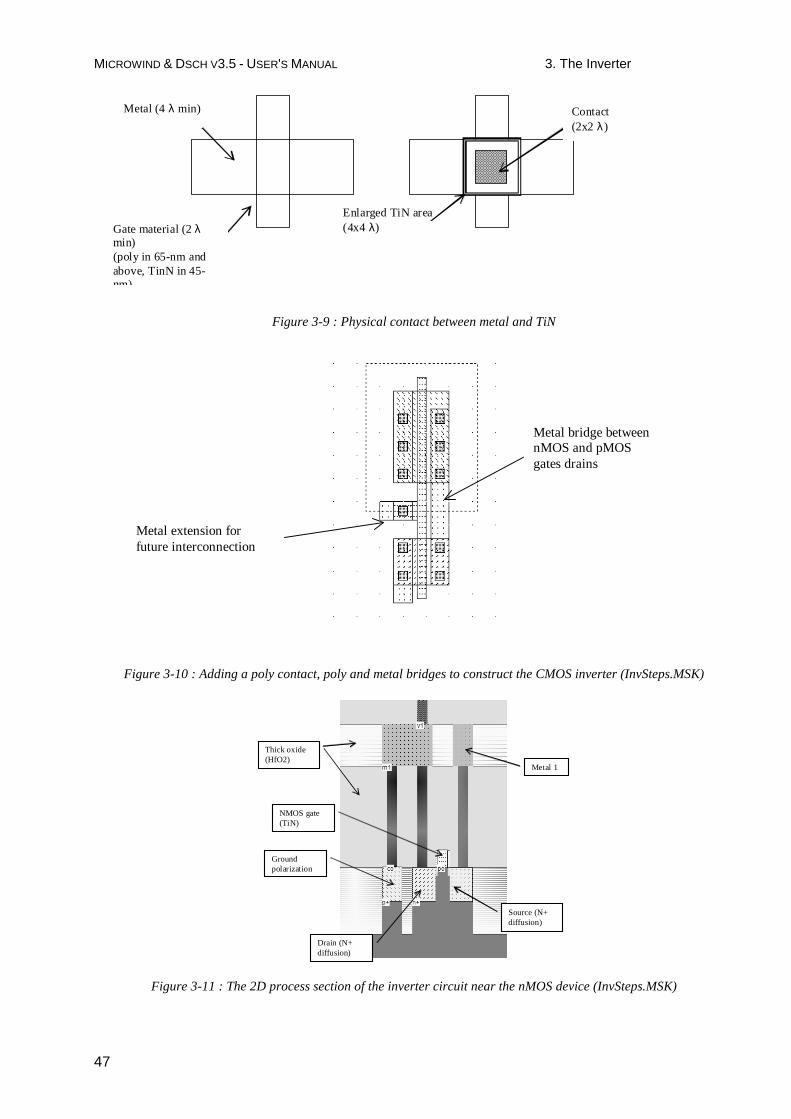
MICROWIND & DSCH V3.5 - USER'S MANUAL 3. The Inverter
47
Gate material (2 λ min) (poly in 65-nm and above, TinN in 45-nm)
Metal (4 λ min) Contact (2x2 λ)
Enlarged TiN area (4x4 λ)
Figure 3-9 : Physical contact between metal and TiN
Metal extension for future interconnection
Metal bridge between nMOS and pMOS gates drains
Figure 3-10 : Adding a poly contact, poly and metal bridges to construct the CMOS inverter (InvSteps.MSK)
Drain (N+ diffusion)
Source (N+ diffusion)
Thick oxide (HfO2)
NMOS gate (TiN)
Metal 1
Ground polarization
Figure 3-11 : The 2D process section of the inverter circuit near the nMOS device (InvSteps.MSK)
MICROWIND & DSCH V3.5 - USER'S MANUAL 3. The Inverter
48
To build an electrical connection, a physical contact is needed. The corresponding layer is called "contact".
You may insert a metal-to-TiN contact in the layout using a direct macro situated in the palette.
The Process Simulator shows the vertical aspect of the layout, as when fabrication has been completed. This
feature is a significant aid to understand the circuit structure and the way layers are stacked on top of each
other. A click of the mouse on the left side of the n-channel device layout and the release of the mouse at the
right side give the cross-section reported in figure 3-10.
Supply Connections
The next design step consists in adding supply connections, that is the positive supply VDD and the ground
supply VSS. We use the metal2 layer (Second level of metallization) to create horizontal supply
connections. Enlarging the supply metal lines reduces the resistance and avoids electrical overstress. The
simplest way to build the physical connection is to add a metal 1 /metal 2 contact that may be found in the
palette. The connection is created by a plug called "via" between metal 2 and metal layers.
The final layout design step consists in adding polarization contacts. These contacts convey the VSS and
VDD voltage supply close to the bulk regions of the device. Remember that the n-well region should always
be polarized to a high voltage to avoid short-circuit between VDD and VSS. Adding the VDD polarization
in the n-well region is a very strict rule.
P+/Pwell contact and bridge to VSS
N+/Nwell contact and bridge to VDD
Via to connect metal2 and metal 1
Figure 3-12 : Adding polarization contacts
Process steps to build the Inverter
At that point, it might be interesting to illustrate the steps of fabrication as they would sequence in a
foundry. MICROWIND includes a 3D process viewer for that purpose. Click Simulate →→→→ Process steps in
3D. The simulation of the CMOS fabrication process is performed, step by step by a click on Next Step.

MICROWIND & DSCH V3.5 - USER'S MANUAL 3. The Inverter
49
Figure 3-13 : The step-by-step fabrication of the Inverter circuit (InvSteps.MSK)
On figure 3-13, the picture on the left represents the nMOS device, pMOS device, common polysilicon gate
and contacts. The picture on the right represents the same portion of layout with the metal layers stacked on
top of the active devices.
Inverter Simulation
The inverter simulation is conducted as follows. Firstly, a VDD supply source (1.0 V) is fixed to the upper
metal 2 supply line, and a VSS supply source (0.0 V) is fixed to the lower metal2 supply line. The
properties are located in the palette menu. Simply click the desired property , and click on the desired
location in the layout. Add a clock on the inverter input node (The default node name clock1 has been
changed into Vin)and a visible property on the output node Vout.
A clock property should be added to this node
VSS property
VDD property
Visible node property
VDD
High VDD VSS Clock
Pulse
Sinus
Visible
Figure 3-14 : Adding simulation properties (InvSteps.MSK)

MICROWIND & DSCH V3.5 - USER'S MANUAL 3. The Inverter
50
Figure 3-15 : Transient simulation of the CMOS inverter (InvSteps.MSK)
The command Simulate →→→→ Run Simulation gives access to the analog simulation. Select the simulation
mode Voltage vs. Time. The analog simulation of the circuit is performed. The time domain waveform,
proposed by default, details the evolution of the voltages in1 and out1 versus time. This mode is also called
transient simulation, as shown in figure 3-15.
The truth-table is verified as follows. A logic “0” corresponds to 0 V a logic “1” to a 1. 0 V. When the input
rises to “1”, the output falls to “0”, with a 7 pico-second delay (7.10-12 second). The reason why the delay
is larger before time 1.0 ns is that the circuit is “warming up” as the voltage supply suddenly rises from 0 to
VDD at time= 0.0ns. The steady-state is reached at time=1.0 ns.
Ring Inverter Simulation
The ring oscillator made from 5 inverters has the property of oscillating naturally. We observe the
oscillating outputs in the circuit of Fig. 3-15 and measure their corresponding frequency. The ring oscillator
circuit can be simulated easily at layout level with Microwind using various technologies. The time-domain
waveform of the output is reported in Fig. 3-16 for 0.8 µm, 0.18 µm and 45-nm technologies (high-speed
option). Although the supply voltage (VDD) has been reduced (VDD is 5V in 0.8 µm, 2V in 0.18µm, and
1.0 V in 45-nm), the gain in frequency improvement is significant.

MICROWIND & DSCH V3.5 - USER'S MANUAL 3. The Inverter
51
Figure 3-15: Schematic diagram and layout of the ring oscillator used for simulation (INV5.MSK)
Use the command File →→→→ Select Foundry to change the configuring technology. Select sequentially the
cmos08.RUL rule file which corresponds to the CMOS 0.8-µm technology, the cmos018.RUL rule file
(0.18µm technology), and eventually cmos45nm.RUL which configures Microwind to the CMOS 45-nm
technology. When you run the simulation, observe the change of VDD and the significant change in
oscillating frequency.
Technology Supply Oscillation Chronograms 0.8 µm 5 V 0.76 GHz
0.18 µm 2 V 7.5 GHz
45 nm 1.0 V 41 GHz
Figure 3-16: Oscillation frequency improvement with the technology scale down (Inv5.MSK)

MICROWIND & DSCH V3.5 - USER'S MANUAL 3. The Inverter
52
Added Features in the Full version
Power estimation Analysis of the inverter consumption, the leakage, etc…
3-state inverter A complete description of the 3-state circuits, with details on the structure, behavior.
Inverter sizing effects Impact of the width and length of MOS devices on the inverter characteristics.
Real-time 3D view
.
Exercises Some basic exercises related to the inverter design and its static/dynamic performances.

MICROWIND & DSCH V3.5 - USER'S MANUAL 4. Basic Gates
53
Introduction
Table 4-1 gives the corresponding symbol to each basic gate as it appears in the logic editor window as well
as the logic description. In this description, the symbol & refers to the logical AND, | to Or, ~to INVERT,
and ^ to XOR. A complete description of basic gate implementation may be found in [Backer].
Name Logic symbol Logic equation INVERTER Out=~in; AND Out=a&b; NAND Out=~(a.b); OR Out=(a|b); NOR Out=~(a|b); XOR Out=a^b; XNOR Out=~(a^b);
Table 4-1. The list of basic gates
The Nand Gate
The truth-table and logic symbol of the NAND gate with 2 inputs are shown below. In DSCH , select the
NAND symbol in the palette, add two buttons and one lamp as shown above. Add interconnects if necessary
to link the button and lamps to the cell pins. Verify the logic behavior of the cell.
in1 in2 Out
0 0 1
0 1 1
1 0 1
1 1 0
Figure 4-1 : The truth table and symbol of the NAND gate
In CMOS design, the NAND gate consists of two nMOS in series connected to two pMOS in parallel. The
schematic diagram of the NAND cell is reported below. The nMOS in series tie the output to the ground for
one single combination A=1, B=1.
4 Basic Gates

MICROWIND & DSCH V3.5 - USER'S MANUAL 4. Basic Gates
54
Figure 4-2 : The truth table and schematic diagram of the CMOS NAND gate design (NandCmos.SCH)
For the three other combinations, the nMOS path is cut, but a least one pMOS ties the output to the supply
VDD. Notice that both nMOS and pMOS devices are used in their best regime: the nMOS devices pass “0”,
the pMOS pass “1”.
You may load the NAND gate design using the command File →→→→ Read→→→→NAND.MSK . You may also
draw the NAND gate manually as for the inverter gate. An alternative solution is to compile directly the
NAND gate into layout with MICROWIND . In this case, complete the following procedure:
In MICROWIND , click on Compile→Compile One
Line. Select the line corresponding to the 2-input
NAND description as shown above. The input and
output names can be by the user modified.
Pmos devices
Nmos devices
Input A
Input B
NAND2 output
Click Compile. The result is reported above.
The compiler has fixed the position of VDD power
supply and the ground VSS. The texts A, B, and S have
also been fixed to the layout. Default clocks are
assigned to inputs A and B.
Figure 4-3 : A NAND cell created by the CMOS compiler.
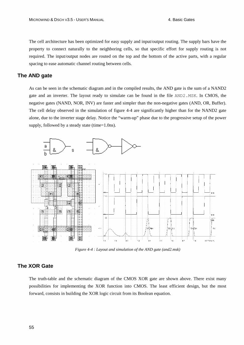
MICROWIND & DSCH V3.5 - USER'S MANUAL 4. Basic Gates
55
The cell architecture has been optimized for easy supply and input/output routing. The supply bars have the
property to connect naturally to the neighboring cells, so that specific effort for supply routing is not
required. The input/output nodes are routed on the top and the bottom of the active parts, with a regular
spacing to ease automatic channel routing between cells.
The AND gate
As can be seen in the schematic diagram and in the compiled results, the AND gate is the sum of a NAND2
gate and an inverter. The layout ready to simulate can be found in the file AND2.MSK. In CMOS, the
negative gates (NAND, NOR, INV) are faster and simpler than the non-negative gates (AND, OR, Buffer).
The cell delay observed in the simulation of figure 4-4 are significantly higher than for the NAND2 gate
alone, due to the inverter stage delay. Notice the “warm-up” phase due to the progressive setup of the power
supply, followed by a steady state (time=1.0ns).
Figure 4-4 : Layout and simulation of the AND gate (and2.msk)
The XOR Gate
The truth-table and the schematic diagram of the CMOS XOR gate are shown above. There exist many
possibilities for implementing the XOR function into CMOS. The least efficient design, but the most
forward, consists in building the XOR logic circuit from its Boolean equation.

MICROWIND & DSCH V3.5 - USER'S MANUAL 4. Basic Gates
56
XOR 2 inputs A B OUT 0 0 0 0 1 1 1 0 1 1 1 0
The proposed solution consists of a transmission-gate implementation of the XOR operator. The truth table
of the XOR can be read as follow: IF B=0, OUT=A, IF B=1, OUT = Inv(A). The principle of the circuit
presented below is to enable the A signal to flow to node N1 if B=1 and to enable the Inv(A) signal to flow
to node N1 if B=0. The node OUT inverts N1, so that we can find the XOR operator. Notice that the nMOS
and pMOS devices situated in the middle of the gate serve as pass transistors.
N1
Figure 4-5 : The schematic diagram of the XOR gate (XORCmos.SCH)
Poor level 0 Poor level 1
Figure 4-6 : Layout and simulation of the XOR gate (XOR.MSK).

MICROWIND & DSCH V3.5 - USER'S MANUAL 4. Basic Gates
57
You may use DSCH to create the cell, generate the Verilog description and compile the resulting text. In
MICROWIND , the Verilog compiler is able to construct the XOR cell as reported in Figure 4-6. You may add
a visible property to the intermediate node which serves as an input of the second inverter.
See how the signal, called internal, is altered by Vtn (when the nMOS is ON) and Vtp (when the pMOS is
ON). Fortunately, the inverter regenerates the signal. However, the output signal “Xor” is not a clean
CMOS signal, and this type of compact design may be abandoned and replaced by more conventional XOR
circuits.
Multiplexor
Multiplexing means transmitting a large amount of information through a smaller number of connections. A
digital multiplexor is a circuit that selects binary information from one of many input logic signals and
directs it to a single input line. The main component of the multiplexor is a basic cell called the transmission
gate. The transmission gate let a signal flow if Enable is asserted.
Sel In0 In1 f 0 x 0 0 0 x 1 1 1 0 x 0 1 1 x 1
Figure 4-7 : The transmission gate used as a multiplexor (MUX.SCH)

MICROWIND & DSCH V3.5 - USER'S MANUAL 4. Basic Gates
58
In DSCH , a transmission gate symbol exists (Figure 4-7). It includes the nMOS, pMOS and inverter cells.
Concerning the layout, the channel length is usually the minimum length available in the technology, and
the width is set large, in order to reduce the parasitic ‘on’ resistance of the gate.
Added Features in the Full version
Basic Gates Truth-table and schematic diagram of the three-input OR gate. AND 4 inputs. Generalization.
Complex Gates The technique produces compact cells with higher performances in terms of spacing and speed than conventional logic circuits. The concept of complex gates is illustrated through concrete examples. The logic implementation of complex gates in DSCH is also described.
Multiplexor Description of a 2n input lines and n selection lines whose bit combinations determine which input is selected. Transmission gate implementation of the 8 to 1 multiplexor.
Interconnect layers and RC behavior
Description of the interconnect materials: metal1..metal6, supply metals, via, RC effects in interconnects, as well as basic formulations for the resistance, inductance and capacitance. Illustration of the crosstalk effect in interconnects.
Exercises XOR, complex gates, design considerations.

MICROWIND & DSCH V3.5 - USER'S MANUAL 5. Arithmetics
59
This chapter introduces basic concepts concerning the design of arithmetic gates. The adder circuit is
presented, with its corresponding layout created manually and automatically. Then the comparator,
multiplier and the arithmetic and logic unit are also discussed. This chapter also includes details on a
student project concerning the design of binary-to-decimal addition and display.
Unsigned Integer format
The two classes of data formats are the integer and real numbers. The integer type is separated into two
formats: unsigned format and signed format. The real numbers are also sub-divided into fixed point and
floating point descriptions. Each data is coded in 8,16 or 32 bits. We consider here unsigned integers, as
described in figure 5-1.
26 25 24 23 20
20 = 1 21 = 2 22 = 4
23 = 8
24 = 16
25 = 32
26 = 64 27 = 128 …. 210 = 1024 215 = 32768 220 = 1048576 230 = 1073741824 231 = 2147483648
Unsigned integer, 8 bit
27 22 21
214 213 24 23 .... 20
Unsigned integer, 16 bit
215 22 21
230 229 24 23 .... 20
Unsigned integer, 32 bit
231 22 21 ..
Figure 5-1 : Unsigned integer format
Half-Adder Gate
The Half-Adder gate truth-table and schematic diagram are shown in Figure 5-2. The SUM function is made
with an XOR gate, the Carry function is a simple AND gate.
HALF ADDER
A B SUM CARRY 0 0 0 0 0 1 1 0 1 0 1 0 1 1 0 1
Figure 5-2 : Truth table and schematic diagram of the half-adder gate (HADD.MSK).
5 Arithmetics
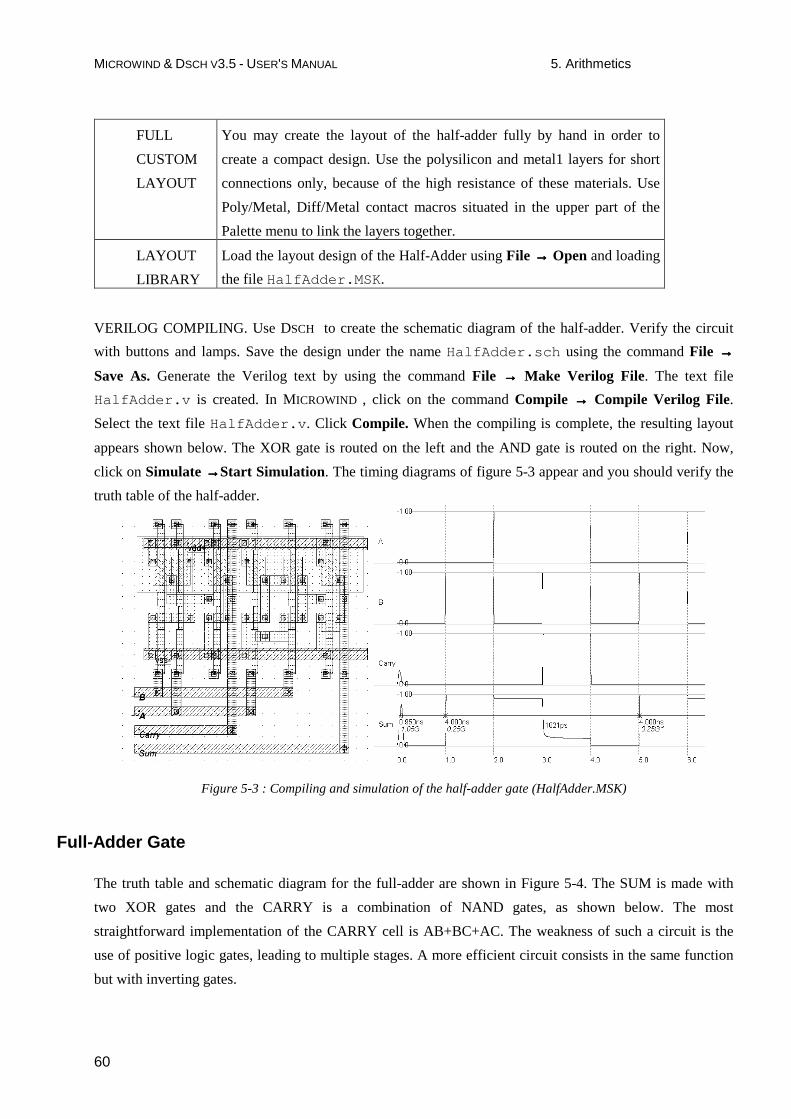
MICROWIND & DSCH V3.5 - USER'S MANUAL 5. Arithmetics
60
FULL
CUSTOM
LAYOUT
You may create the layout of the half-adder fully by hand in order to
create a compact design. Use the polysilicon and metal1 layers for short
connections only, because of the high resistance of these materials. Use
Poly/Metal, Diff/Metal contact macros situated in the upper part of the
Palette menu to link the layers together.
LAYOUT
LIBRARY
Load the layout design of the Half-Adder using File →→→→ Open and loading
the file HalfAdder.MSK .
VERILOG COMPILING. Use DSCH to create the schematic diagram of the half-adder. Verify the circuit
with buttons and lamps. Save the design under the name HalfAdder.sch using the command File →→→→
Save As. Generate the Verilog text by using the command File →→→→ Make Verilog File. The text file
HalfAdder.v is created. In MICROWIND , click on the command Compile →→→→ Compile Verilog File.
Select the text file HalfAdder.v . Click Compile. When the compiling is complete, the resulting layout
appears shown below. The XOR gate is routed on the left and the AND gate is routed on the right. Now,
click on Simulate →→→→Start Simulation. The timing diagrams of figure 5-3 appear and you should verify the
truth table of the half-adder.
Figure 5-3 : Compiling and simulation of the half-adder gate (HalfAdder.MSK)
Full-Adder Gate
The truth table and schematic diagram for the full-adder are shown in Figure 5-4. The SUM is made with
two XOR gates and the CARRY is a combination of NAND gates, as shown below. The most
straightforward implementation of the CARRY cell is AB+BC+AC. The weakness of such a circuit is the
use of positive logic gates, leading to multiple stages. A more efficient circuit consists in the same function
but with inverting gates.
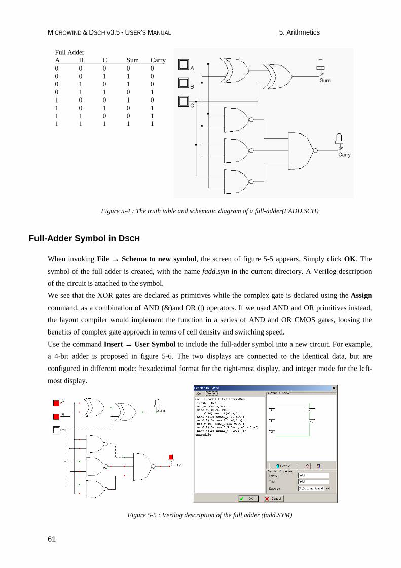
MICROWIND & DSCH V3.5 - USER'S MANUAL 5. Arithmetics
61
Full Adder A B C Sum Carry 0 0 0 0 0 0 0 1 1 0 0 1 0 1 0 0 1 1 0 1 1 0 0 1 0 1 0 1 0 1 1 1 0 0 1 1 1 1 1 1
Figure 5-4 : The truth table and schematic diagram of a full-adder(FADD.SCH)
Full-Adder Symbol in D SCH
When invoking File →→→→ Schema to new symbol, the screen of figure 5-5 appears. Simply click OK . The
symbol of the full-adder is created, with the name fadd.sym in the current directory. A Verilog description
of the circuit is attached to the symbol.
We see that the XOR gates are declared as primitives while the complex gate is declared using the Assign
command, as a combination of AND (&)and OR (|) operators. If we used AND and OR primitives instead,
the layout compiler would implement the function in a series of AND and OR CMOS gates, loosing the
benefits of complex gate approach in terms of cell density and switching speed.
Use the command Insert →→→→ User Symbol to include the full-adder symbol into a new circuit. For example,
a 4-bit adder is proposed in figure 5-6. The two displays are connected to the identical data, but are
configured in different mode: hexadecimal format for the right-most display, and integer mode for the left-
most display.
Figure 5-5 : Verilog description of the full adder (fadd.SYM)

MICROWIND & DSCH V3.5 - USER'S MANUAL 5. Arithmetics
62
Figure 5-6 : Schematic diagram of the four-bit adder and some examples of results (Add4.SCH).
Comparator
The truth table and the schematic diagram of the comparator are given below. The A=B equality represents
an XNOR gate, and A>B, A<B are operators obtained by using inverters and AND gates.
Comparator A B A>B A<B A=B 0 0 0 0 1 0 1 0 1 0 1 0 1 0 0 1 1 0 0 1
Figure 5-7 : The truth table and schematic diagram of the comparator (COMP.SCH).
Using DSCH , the logic circuit of the comparator is designed and verified at logic level. Then the conversion
into Verilog is invoked (File →→→→ Make verilog File). MICROWIND compiles the verilog text into layout. The
simulation of the comparator is given in Figure 5-8. The XNOR gate is located at the left side of the design.
The inverter and NOR gates are at the right side. After the initialization, A=B rises to 1. The clocks A and B
produce the combinations 00,01,10 and 11.

MICROWIND & DSCH V3.5 - USER'S MANUAL 5. Arithmetics
63
Figure 5-8 : Simulation of a comparator (COMP.MSK).
Fault Injection and test vector extraction
Design of logic integrated circuits in CMOS technology is becoming more and more complex since VLSI is
the interest of many electronic IC users and manufacturers. A common problem to be solved by designers,
manufacturers and users is the testing of these ICs. In DSCH 3.5, we introduce the concept of fault,
concentrate on stuck-at-0 and stuck-at-1 hypothesis, and show how these faults may appear. Then, using
DSCH, we show how to build a reference truth-table, and how to simulate these faults applied to input and
output nodes of the circuit under test. We investigate how test patterns detect these faults. The ultimate goal

MICROWIND & DSCH V3.5 - USER'S MANUAL 5. Arithmetics
64
is to classify the efficiency of test patterns, in order to select the most efficient test vectors, and therefore
reduce the number of test patterns.
Faults considered in DSCH are called “stuck-at” faults. We consider two types of “Stuck-at” : stuck-at-0
and stuck-at-1 faults. Figure 5-9 illustrates a possible origin for a node stuck at 0 voltage: the
implementation is close to a VSS node (here situated close, same layer), and a faulty metal bridge makes a
robust connection to the ground.
Designed interconnects
Fabricated interconnects with stuck-at-0 fault
Bridge
Node under test
VSS
Figure 5-9 : Physical origin of a node fault stuck at 0.
There are several ways to nominate stuck-at faults, all having the same meaning. In DSCH, we shall use
“N@0” for node N stuck-at 0 and “N@1” for node N stuck-at-1. In DSCH version 3.5, build a simple circuit
as shown in Fig. 5-10, including 2 inputs and one output, and click “Simulate”→ “Logic Circuit Testing”.
The screen shown in Fig. 5-11 corresponds to the construction of the reference truth-table. In the table
situated in the left part of the screen, all inputs and outputs are displayed, and the input values are pre-
positioned. In the case of the AND gate, two inputs A and B are listed.
Figure 5-10 : testing an AND gate
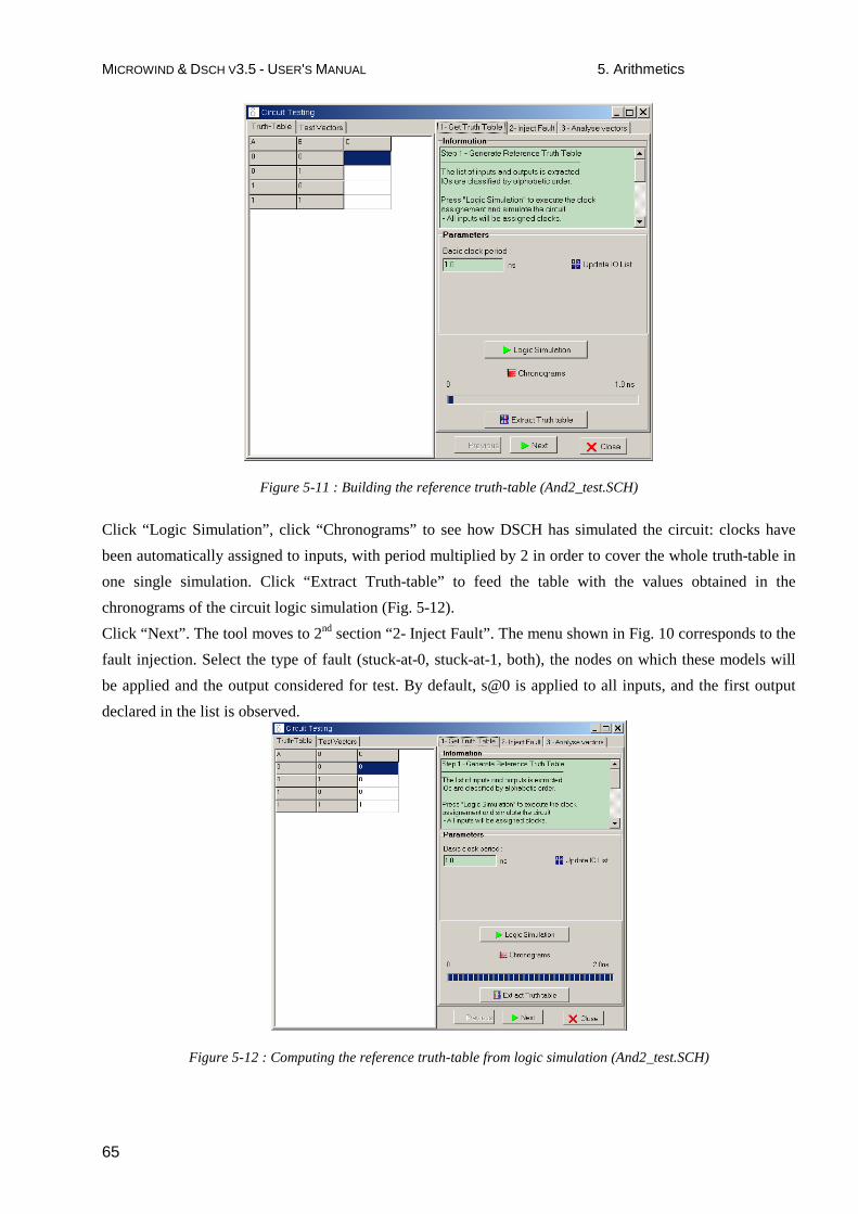
MICROWIND & DSCH V3.5 - USER'S MANUAL 5. Arithmetics
65
Figure 5-11 : Building the reference truth-table (And2_test.SCH)
Click “Logic Simulation”, click “Chronograms” to see how DSCH has simulated the circuit: clocks have
been automatically assigned to inputs, with period multiplied by 2 in order to cover the whole truth-table in
one single simulation. Click “Extract Truth-table” to feed the table with the values obtained in the
chronograms of the circuit logic simulation (Fig. 5-12).
Click “Next”. The tool moves to 2nd section “2- Inject Fault”. The menu shown in Fig. 10 corresponds to the
fault injection. Select the type of fault (stuck-at-0, stuck-at-1, both), the nodes on which these models will
be applied and the output considered for test. By default, s@0 is applied to all inputs, and the first output
declared in the list is observed.
Figure 5-12 : Computing the reference truth-table from logic simulation (And2_test.SCH)

MICROWIND & DSCH V3.5 - USER'S MANUAL 5. Arithmetics
66
Figure 5-13 : Two logic simulations are necessary to extract the response to the A@0 and B@0 faults (And2_test.SCH)
Click “Generate Faults” to list the desired faults in the test vector grid situated on the left of the screen.
Notice that each column corresponds to one test vector. As we have 2 inputs, we have 4 columns, each
corresponding to one test vector for inputs AB, respectively 00, 01, 10, and 11. The two faults considered
here are A@0 and B@0.
In order to compute the response of the circuit to the A@0 and B@0 faults, proceed as follow:
- Click “Simulate fault n°1 – A@0”. Click “Chronograms” to see the response. The node A is stuck-at-0,
and consequently, the output C is 0.
Node A “Stuck-at-0
Figure 5-14 : Chronograms showing the node A stuck-at-0 (And2_test.SCH)
- Click “Extract Fault Response”. The logic values are transferred to the corresponding line.
- Click “Simulate fault n°2 – B@0”.
- Click “Extract Fault Response”. The circuit response to the 2nd fault is also transferred
By selecting “Stuck-at 0 & stuck-at 1”, and applying it to Inputs & Outputs, we obtain the following
response to the 6 faults:

MICROWIND & DSCH V3.5 - USER'S MANUAL 5. Arithmetics
67
Figure 5-15 : Response of the circuit to all possible stuck-at faults (And2_test.SCH)
Figure 5-16 : Detection score for all test patterns (And2_test.SCH)
Click “Next”. The tool moves to 3rd section “3- Analyse Vectors”. Click “Highlight Detection Vectors”.
From the results computed in Fig. 5-15, we may see that not all test vectors have the same detection
efficiency. The test vector <11> (last column) is able to detect 4 faults upon the total of 6. This means that
applying 11 to inputs A,B leads to a result on C different from the reference logic value 1 (line “C(Fault-
Free)”, which enables the test vector 11 to alert the user from the possibility of 4 possible faults: A@0,
B@0, B@1, C@0. All faults may be tested (100% coverage) using three vectors: 01, 10 and 11.

MICROWIND & DSCH V3.5 - USER'S MANUAL 5. Arithmetics
68
Added Features in the Full version
Adders Full layout of the 4-bit adder. Structure of the carry look-ahead adder. Details on the routing and supply strategy.
Arithmetic and Logic Units
Basic principles of micro-operations on 8 bit format.
Testing Complete case studies with full-adder, complex gates

MICROWIND & DSCH V3.5 - USER'S MANUAL 6. Microcontroller Model
69
6 Microcontroller Model
This chapter details the implementation of a simplified model of two microcontroller: the 8051 from Intel
and the 16f54 from PIC.
8051 Model
The 8051 core includes an arithmetic and logic unit to support a huge set of instructions. Most of the data
format is in 8 bit format. We consider here the following instructions, listed in table 1. Some instructions do
not appear in this list, such as the multiplication and division.
Mnemonic Type Description CLR Clear Clear the accumulator CPL Complement Complements the accumulator, a bit or a memory contents.
All the bits will be reversed. ADD Addition Add the operand to the value of the accumulator, leaving the
resulting value in the accumulator. SUBB Substractor Subtracts the operand to the value of the accumulator, leaving
the resulting value in the accumulator. INC Increment Increment the content of the accumulator, the register or the
memory. DEC Decrement Decrement the content of the accumulator, the register or the
memory. XRL XOR operator Exclusive OR operation between the accumulator and the
operand, leaving the resulting value in the accumulator. ANL AND operator AND operation between the accumulator and the operand,
leaving the resulting value in accumulator. ORL OR operator OR operation between the accumulator and the operand,
leaving the resulting value in accumulator. RR Rotate right Shifts the bits of the accumulator to the right. The bit 0 is
loaded into bit 7. RL Rotate left Shifts the bits of the accumulator to the left. The bit 7 is
loaded into bit 0.
Table 1. Some important instructions implemented in the ALU of the 8051 micro-controller
Accumulator A
Arithmetic and Logic Unit
8 bits 8 bits
Result S
8 bits
OpCode input
Registers R0..R7
Immediate value
Memory contents
CarryIn
CarryOut

MICROWIND & DSCH V3.5 - USER'S MANUAL 6. Microcontroller Model
70
Figure 6-1 : The arithmetic and logic unit of the 8051
For example:
• ADD A,R0 (Opcode 0x28) overwrites the accumulator with the result of the addition of A and the
content of R0.
• SUBB A,#2 (Opcode 0x94 0x02) overwrites the accumulator with the result of the subtraction of A
and the sum of the Carry and the byte 0x02.
• INC A (0x04) increments the content of the accumulator.
• DEC A (0x14) Decrements the content of the accumulator.
• ANL A,#10 (0x54) overwrites the accumulator with by the AND-gating of A and the constant
0x10.
• ORL A,R7 (0x4F) overwrites the accumulator with by the OR-gating of A and the content of R7.
• XRL A, R1 (0x69) overwrites the accumulator with the result of the XOR-gating of A and the
content of the internal register R1.
Inside the 8051
A simplified model of the 8-bit micro-controller 8051 exists through the symbol “8051.SYM” accessible
using the command Insert →→→→ User Symbol. The symbol is also directly accessible through the symbol
palette starting version 3.5.
Figure 6-2 : Access to the 8051 symbol from the palette, in the “Advanced” list
The symbol consists mainly of general purpose input/output ports (P0,P1,P2 and P3), a clock and a reset
control signals. The basic connection consists of a clock on the Clock input and a button on the Reset input
(Figure 5).

MICROWIND & DSCH V3.5 - USER'S MANUAL 6. Microcontroller Model
71
Figure 6-3 : The 8051 symbol and its embedded software (8051.SCH)
After a double-click in the symbol, the embedded code appears. That code may be edited and modified
(Figure 6-3). When the button Assembly is pressed, the assembly text is translated into executable binary
format. Once the logic simulation is running, the code is executed as soon as the reset input is deactivated.
The value of the program counter, the accumulator A, the current op_code and the registers is displayed.
Minimum features for running the 8051
The user should
1. Add a clock on input “Clock”
2. Add a button on input “RST”
3. Double click on the symbol and click “Assembly” so that the editable text of the code is converted into
assembly code
4. Run the logic simulator
5. Click the “RST” button (RST=1, button red) so that Reset is INACTIVE
In the chronograms of Fig. 6-4, the accumulator variations versus the time are displayed. It can be noticed
that this core operates with one single clock cycle per instruction, except for some instructions such as
MOV (Move data) and AJMP (Jump to a specific address).

MICROWIND & DSCH V3.5 - USER'S MANUAL 6. Microcontroller Model
72
Click “Assembly” to compute
Figure 6-4 : The simulation of the arithmetic and logic operation using the 8051 micro-controller (8051.SCH)
Traffic light Example
An example of code and schematic diagram for traffic light control is proposed below. Notice the subroutine
call through the instruction “AJUMP”.
Figure 6-5 : A simple code for 8051 micro-controller for traffic light control (8051_traffic_lights.sch)
Ports are activated using control commands such as “MOV P3,#0”, while port input pins are tested through
the instruction such as “JB P2.2,URG”. See table 2 for the complete code embedded in the 8051 processor.
// Traffic Lights E. Sicard // 11.nov.01 L1 MOV P3,#84H ACALL TEMPO Feu1=r,F2=vert JB P2.2,URG JB P2.1,FJ AJMP L1
FJ1 ACALL TEMPO MOV P3,#50H ACALL TEMPO j, r MOV P3,#90H ACALL TEMPO r, r MOV P3,#84H
Temporisation TEMPO NOP NOP NOP NOP NOP NOP NOP

MICROWIND & DSCH V3.5 - USER'S MANUAL 6. Microcontroller Model
73
FJ ACALL TEMPO MOV P3,#88H Feu1=r,F2=jaune ACALL TEMPO MOV P3,#90H ACALL TEMPO r, r L2 MOV P3,#30H v , r JB P2.2,URG JB P2.0,FJ1 AJMP L2
AJMP L1
RET Urgence URG MOV P3,#48H NOP MOV P3,#0 JNB P2.2,L1 AJMP URG
Table 6-2. Code embedded in the traffic light controller (8051_traffic_lights.sch)
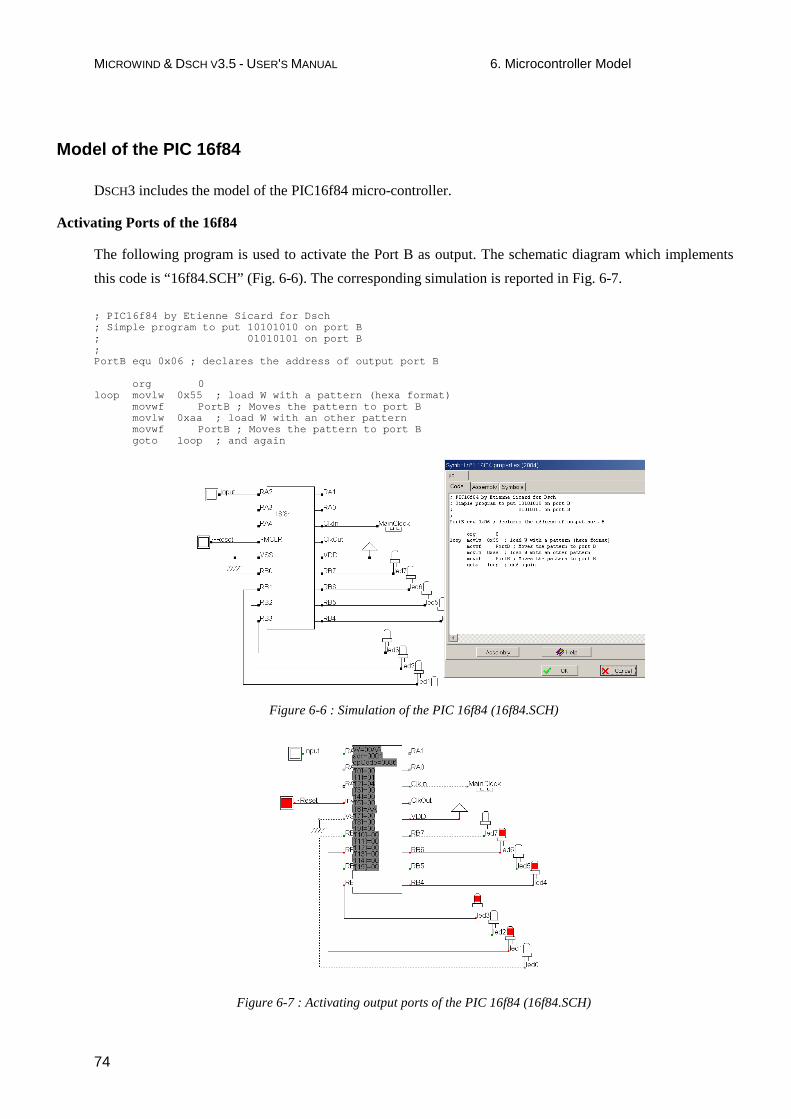
MICROWIND & DSCH V3.5 - USER'S MANUAL 6. Microcontroller Model
74
Model of the PIC 16f84
DSCH3 includes the model of the PIC16f84 micro-controller.
Activating Ports of the 16f84
The following program is used to activate the Port B as output. The schematic diagram which implements
this code is “16f84.SCH” (Fig. 6-6). The corresponding simulation is reported in Fig. 6-7.
; PIC16f84 by Etienne Sicard for Dsch ; Simple program to put 10101010 on port B ; 01010101 on port B ; PortB equ 0x06 ; declares the address of output por t B org 0 loop movlw 0x55 ; load W with a pattern (hexa fo rmat) movwf PortB ; Moves the pattern to port B movlw 0xaa ; load W with an other pattern movwf PortB ; Moves the pattern to port B goto loop ; and again
Figure 6-6 : Simulation of the PIC 16f84 (16f84.SCH)
Figure 6-7 : Activating output ports of the PIC 16f84 (16f84.SCH)

MICROWIND & DSCH V3.5 - USER'S MANUAL 7. Latches
75
This chapter details the structure and behavior of latch circuits. The RS Latch, the D Latch, the
edge-sensitive register and the counter are presented.
Basic Latch
The basis for storing an elementary binary value is called a latch. The simplest CMOS circuit is
made from 2 inverters.
Q
Q=10
1
2 stablememorystates
Q=01
0
Figure 7-1 : Elementary memory cell based on an inverter loop
RS Latch
The RS Latch, also called Set-Reset Flip Flop (SR FF), transforms a pulse into a continuous
state. The RS latch can be made up of two interconnected NOR or NAND gates, inspired from
the two chained inverters of figure 6-2. In the case of RS-NOR, the Reset and Set inputs are
active high. The memory state corresponds to Reset=Set=0. The combination Reset=Set=1
should not be used, as it means that Q should be Reset and Set at the same time.
RS Latch (NOR) R S Q nQ 0 0 Q nQ 0 1 1 0 1 0 0 1 1 1 1 1
7 Latches
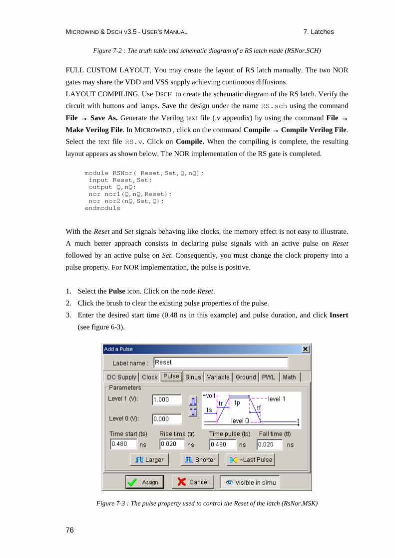
MICROWIND & DSCH V3.5 - USER'S MANUAL 7. Latches
76
Figure 7-2 : The truth table and schematic diagram of a RS latch made (RSNor.SCH)
FULL CUSTOM LAYOUT. You may create the layout of RS latch manually. The two NOR
gates may share the VDD and VSS supply achieving continuous diffusions.
LAYOUT COMPILING. Use DSCH to create the schematic diagram of the RS latch. Verify the
circuit with buttons and lamps. Save the design under the name RS.sch using the command
File →→→→ Save As. Generate the Verilog text file (.v appendix) by using the command File →→→→
Make Verilog File. In MICROWIND , click on the command Compile →→→→ Compile Verilog File.
Select the text file RS.v . Click on Compile. When the compiling is complete, the resulting
layout appears as shown below. The NOR implementation of the RS gate is completed.
module RSNor( Reset,Set,Q,nQ); input Reset,Set; output Q,nQ; nor nor1(Q,nQ,Reset); nor nor2(nQ,Set,Q); endmodule
With the Reset and Set signals behaving like clocks, the memory effect is not easy to illustrate.
A much better approach consists in declaring pulse signals with an active pulse on Reset
followed by an active pulse on Set. Consequently, you must change the clock property into a
pulse property. For NOR implementation, the pulse is positive.
1. Select the Pulse icon. Click on the node Reset.
2. Click the brush to clear the existing pulse properties of the pulse.
3. Enter the desired start time (0.48 ns in this example) and pulse duration, and click Insert
(see figure 6-3).
Figure 7-3 : The pulse property used to control the Reset of the latch (RsNor.MSK)

MICROWIND & DSCH V3.5 - USER'S MANUAL 7. Latches
77
Figure 7-4 : Layout of the RS latch made (RSNor.MSK)
4. Repeat the same procedure to change the clock into a pulse for node Set. The start time is
now fixed to 1.48 ns to generate a pulse later than for the Reset signal.
5. Click on Simulate →→→→Start Simulation. The timing diagrams of figure 6-4 appear.
In the simulation of figure 6-4, a positive pulse on Set turns Q to a stable high state. Notice that
when Set goes to 0, Q remains at 1, which is called the ‘memory’ state. When a positive pulse
occurs on Reset, Q goes low, nQ goes high. In this type of simulation, the combination
Reset=Set=1 is not present.
Edge Trigged Latch
This edge-trigged latch is one of the most widely used cells in microelectronics circuit design.
The cell structure comprises two master-slave basic memory stages. The most compact
implementation of the edge-trigged latch is reported below (figure 6-5). The schematic diagram
is based on inverters and pass-transistors. On the left side, the two chained inverter are in
memory state when the pMOS loop transistor P1 is on, that is when Clk=0. The two-chained
inverters on the right side act in an opposite way. The reset function is obtained by a direct
ground connection of the master and slave memories, using nMOS devices.
When clock is high, the master latch is updated to a new value of the input D. The slave latch
produces to the output Q the previous value of D. When clock goes down, the master latch
turns to memory state. The slave circuit is updated. The change of the clock from 1 to 0 is the
active edge of the clock. This type of latch is a negative edge flip flop.

MICROWIND & DSCH V3.5 - USER'S MANUAL 7. Latches
78
Use the Verilog compiler to generate the edge-trigged latch description in Verilog format, or by
creating a schematic diagram including the “D” register symbol, in the symbol palette of DSCH .
Master=0Q=0
Slave transparent
Slave =0
Q=0
Master transparent
Clock =0
Clock =1
Clock =0
Master=1Slave transparent
Q updated to 1
Fall edge of the clock
Figure 7-5 : The edge-trigged latch and its logic simulation (Dreg.MSK)

MICROWIND & DSCH V3.5 - USER'S MANUAL 7. Latches
79
As can be seen, the register is built up from one single call to the primitive dreg . For
simulation:
• Reset is active on a level 1. Reset is activated twice, at the beginning and later, using a
piece-wise linear description included in the pulse property.
• Clk is a clock with 10ns at 0 and 10ns at 1.
• D is the data chosen here not synchronized with Clk, in order to observe various
behaviors of the register.
To compile the DREG file, use the command Compile→→→→Compile Verilog Text. The
corresponding layout is reported below. The piece-wise-linear data is transferred to the text
label “Reset” appearing in the lower corner of the D flip flop layout of figure 6-6.
For testing the Dreg, the Reset signal is activated twice, at the beginning and later, using a
piece-wise linear property (figure 6-6). The Clock signal has a 2 ns period. D is the data chosen
here not synchronized with Clock, in order to observe various behaviors of the register.
The simulation of the edge-trigged D-register is reported in figure 6-6. The signals Q and nQ
always act in opposite. When Reset is asserted, the output Q is 0, nQ is 1. When Reset is not
active, Q takes the value of D at a fall edge of the clock. For all other cases, Q and nQ remain in
memory state. The latch is thus sensitive to the fall edge of the clock.
Master memory loopSlave memory loop
Reset master Reset slave
Figure 7-6 : Compiled version of the Edge-trigged D Flip Flop (DregCompile.MSK)

MICROWIND & DSCH V3.5 - USER'S MANUAL 7. Latches
80
Figure 7-7 : Piece-wise-linear property used for sophisticated control of input signals
(DregCompile.MSK)
Data transferred to Q at the fall edge of Clock
Asynchronous reset of the D-Flip-Flop
Figure 7-8 : Simulation of the DREG cell (DregCompile.MSK)
Added Features in the Full version
Latches The truth table and schematic diagram of the static D latch, also called Static D-Flip-Flop are described. The main characteristics of the latch switching are presented.
Counters The one-bit counter is able to produce a signal featuring half the frequency of a clock. The implementation is detailed. Up and down counters are also described.
Registers Shift registers, serial registers are described.
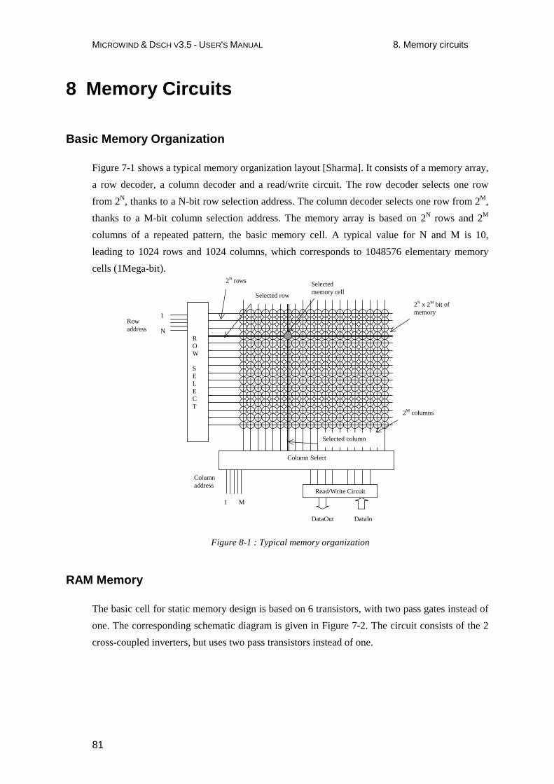
MICROWIND & DSCH V3.5 - USER'S MANUAL 8. Memory circuits
81
Basic Memory Organization
Figure 7-1 shows a typical memory organization layout [Sharma]. It consists of a memory array,
a row decoder, a column decoder and a read/write circuit. The row decoder selects one row
from 2N, thanks to a N-bit row selection address. The column decoder selects one row from 2M,
thanks to a M-bit column selection address. The memory array is based on 2N rows and 2M
columns of a repeated pattern, the basic memory cell. A typical value for N and M is 10,
leading to 1024 rows and 1024 columns, which corresponds to 1048576 elementary memory
cells (1Mega-bit).
ROW
SELECT
Column Select
Read/Write Circuit
1 M
Columnaddress
DataOut DataIn
1
N
2N rows
Rowaddress
2N x 2M bit ofmemory
2M columns
Selectedmemory cellSelected row
Selected column
Figure 8-1 : Typical memory organization
RAM Memory
The basic cell for static memory design is based on 6 transistors, with two pass gates instead of
one. The corresponding schematic diagram is given in Figure 7-2. The circuit consists of the 2
cross-coupled inverters, but uses two pass transistors instead of one.
8 Memory Circuits

MICROWIND & DSCH V3.5 - USER'S MANUAL 8. Memory circuits
82
Figure 8-2 : The layout of the 6 transistor static memory cell (RAM6T.SCH)
Figure 8-3 : An array of 6T memory cells, with 4 rows and 4 columns (RAM6T.SCH)
The cell has been designed to be duplicated in X and Y in order to create a large array of cells.
Usual sizes for Megabit SRAM memories are 256 column x 256 rows or higher. A modest
arrangement of 4x4 RAM cells is proposed in figure 7-3. The selection lines WL concern all the
cells of one row. The bit lines BL and ~BL concern all the cells of one column.
The RAM layout is given in Figure 7-4. The BL and ~BL signals are made with metal2 and
cross the cell from top to bottom. The supply lines are horizontal, made with metal3. This
allows easy matrix-style duplication of the RAM cell.
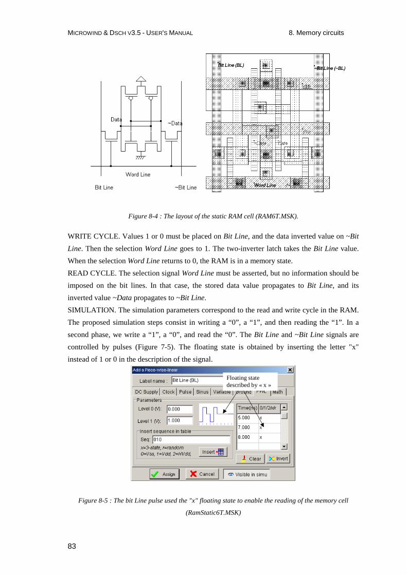
MICROWIND & DSCH V3.5 - USER'S MANUAL 8. Memory circuits
83
Figure 8-4 : The layout of the static RAM cell (RAM6T.MSK).
WRITE CYCLE. Values 1 or 0 must be placed on Bit Line, and the data inverted value on ~Bit
Line. Then the selection Word Line goes to 1. The two-inverter latch takes the Bit Line value.
When the selection Word Line returns to 0, the RAM is in a memory state.
READ CYCLE. The selection signal Word Line must be asserted, but no information should be
imposed on the bit lines. In that case, the stored data value propagates to Bit Line, and its
inverted value ~Data propagates to ~Bit Line.
SIMULATION. The simulation parameters correspond to the read and write cycle in the RAM.
The proposed simulation steps consist in writing a “0”, a “1”, and then reading the “1”. In a
second phase, we write a “1”, a “0”, and read the “0”. The Bit Line and ~Bit Line signals are
controlled by pulses (Figure 7-5). The floating state is obtained by inserting the letter "x"
instead of 1 or 0 in the description of the signal.
Floating state described by « x »
Figure 8-5 : The bit Line pulse used the "x" floating state to enable the reading of the memory cell
(RamStatic6T.MSK)
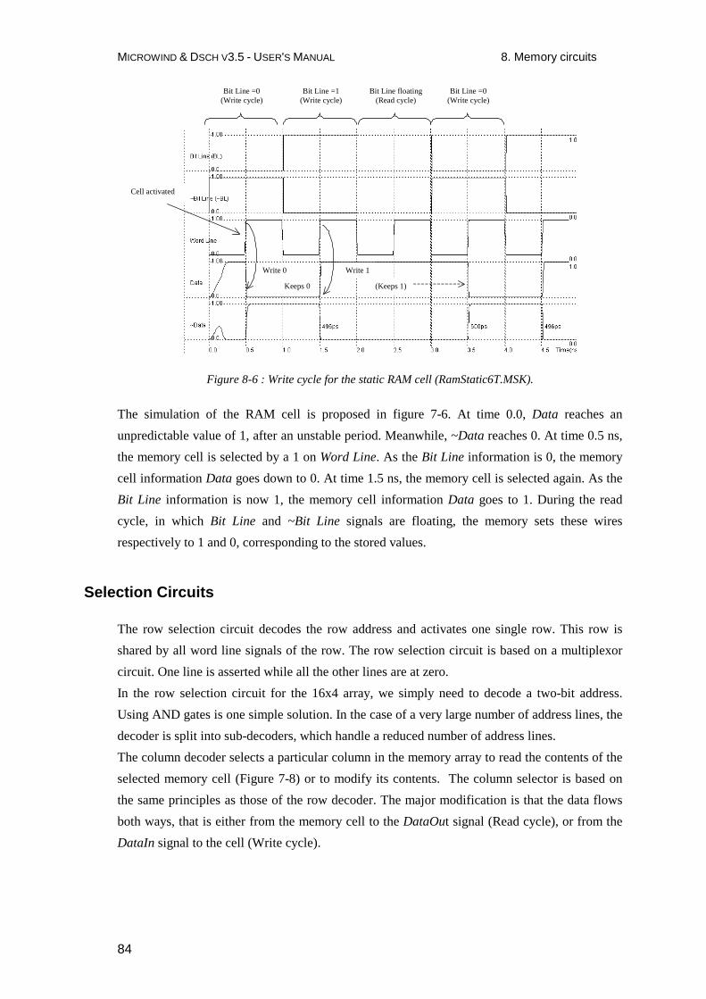
MICROWIND & DSCH V3.5 - USER'S MANUAL 8. Memory circuits
84
Bit Line floating (Read cycle)
Bit Line =0 (Write cycle)
Cell activated
Write 0
Keeps 0
Write 1
(Keeps 1)
Bit Line =1 (Write cycle)
Bit Line =0 (Write cycle)
Figure 8-6 : Write cycle for the static RAM cell (RamStatic6T.MSK).
The simulation of the RAM cell is proposed in figure 7-6. At time 0.0, Data reaches an
unpredictable value of 1, after an unstable period. Meanwhile, ~Data reaches 0. At time 0.5 ns,
the memory cell is selected by a 1 on Word Line. As the Bit Line information is 0, the memory
cell information Data goes down to 0. At time 1.5 ns, the memory cell is selected again. As the
Bit Line information is now 1, the memory cell information Data goes to 1. During the read
cycle, in which Bit Line and ~Bit Line signals are floating, the memory sets these wires
respectively to 1 and 0, corresponding to the stored values.
Selection Circuits
The row selection circuit decodes the row address and activates one single row. This row is
shared by all word line signals of the row. The row selection circuit is based on a multiplexor
circuit. One line is asserted while all the other lines are at zero.
In the row selection circuit for the 16x4 array, we simply need to decode a two-bit address.
Using AND gates is one simple solution. In the case of a very large number of address lines, the
decoder is split into sub-decoders, which handle a reduced number of address lines.
The column decoder selects a particular column in the memory array to read the contents of the
selected memory cell (Figure 7-8) or to modify its contents. The column selector is based on
the same principles as those of the row decoder. The major modification is that the data flows
both ways, that is either from the memory cell to the DataOut signal (Read cycle), or from the
DataIn signal to the cell (Write cycle).

MICROWIND & DSCH V3.5 - USER'S MANUAL 8. Memory circuits
85
ROW
SELECT
1
N
2N rows
Rowaddress
Selected row (Word Line)
MemRow Cell
Heightfixed bythe Mem
size
Freewidth
Memwidth
Memheight
WordLineWord
Line
Figure 8-7 : The row selection circuit
Column Select
Read/Write Circuit
1 M
Columnaddress
DataOut DataIn
2M columns
Selectedmemory cell
Selected column
Control
Figure 8-8 : The column selection circuit principles
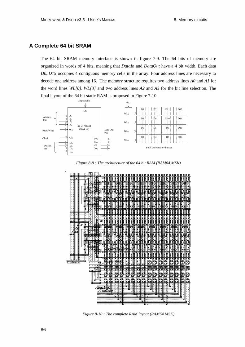
MICROWIND & DSCH V3.5 - USER'S MANUAL 8. Memory circuits
86
A Complete 64 bit SRAM
The 64 bit SRAM memory interface is shown in figure 7-9. The 64 bits of memory are
organized in words of 4 bits, meaning that DataIn and DataOut have a 4 bit width. Each data
D0..D15 occupies 4 contiguous memory cells in the array. Four address lines are necessary to
decode one address among 16. The memory structure requires two address lines A0 and A1 for
the word lines WL[0]..WL[3] and two address lines A2 and A3 for the bit line selection. The
final layout of the 64 bit static RAM is proposed in Figure 7-10.
Address bus
A0
A1
WE Read/Write
Clk Clock
Do0
Do1
Data Out bus
CE
Chip Enable
Do2
Do3
Di0
Di1
Di3 Data In bus
Di2
A2
A3
64 bit SRAM (16x4 bit)
D0
D1
D2
D3
D4
D5
D6
D7
D8
D9
D10
D11
D12
D13
D14
D15
Each Data has a 4 bit size
WL3
WL2
WL1
WL0
A0..1
Figure 8-9 : The architecture of the 64 bit RAM (RAM64.MSK)
Figure 8-10 : The complete RAM layout (RAM64.MSK)

MICROWIND & DSCH V3.5 - USER'S MANUAL 8. Memory circuits
87
Dynamic RAM Memory
The dynamic RAM memory has only one transistor, in order to improve the memory matrix
density by almost one order of magnitude. The storage element is no longer the stable inverter
loop, as for the static RAM, but only a capacitor Cs, also called the storage capacitor. The write
and hold operation for a "1" is shown in figure 7-11. The data is set on the bit line, the word
line is then activated and Cs is charged. As the pass transistor is n-type, the analog value
reaches VDD-Vt. When WL is inactive, the storage capacitor Cs holds the "1".
Precharged to Vp
Vp+∆V
Precharged to Vp
Vp-∆V
Figure 8-11 : Simulation of the Read cycle for the 1 transistor dynamic RAM cell (RAM1T.SCH)
The reading cycle is destructive for the stored information. Suppose that Cs holds a 1. The bit
line is precharged to a voltage Vp (Usually around VDD/2). When the word line is active, a
communication is established between the bit line, loaded by capacitor CBL, and the memory,
loaded by capacitor CS. The charges are shared between these nodes, and the result is a small
increase of the voltage Vp by ∆V, thanks to the injection of some charges from the memory.
The cross-section of the DRAM capacitor is given in figure 7-12. The bit line is routed in
metal2, and is connected to the cell through a metal1 and diffusion contact. The word line is the
polysilicon gate. On the right side, the storage capacitor is a sandwich of conductor material
connected to the diffusion, a thin oxide (SiO2 in this case) and a second conductor that fills the
capacitor and is connected to ground by a contact to the first level of metal.
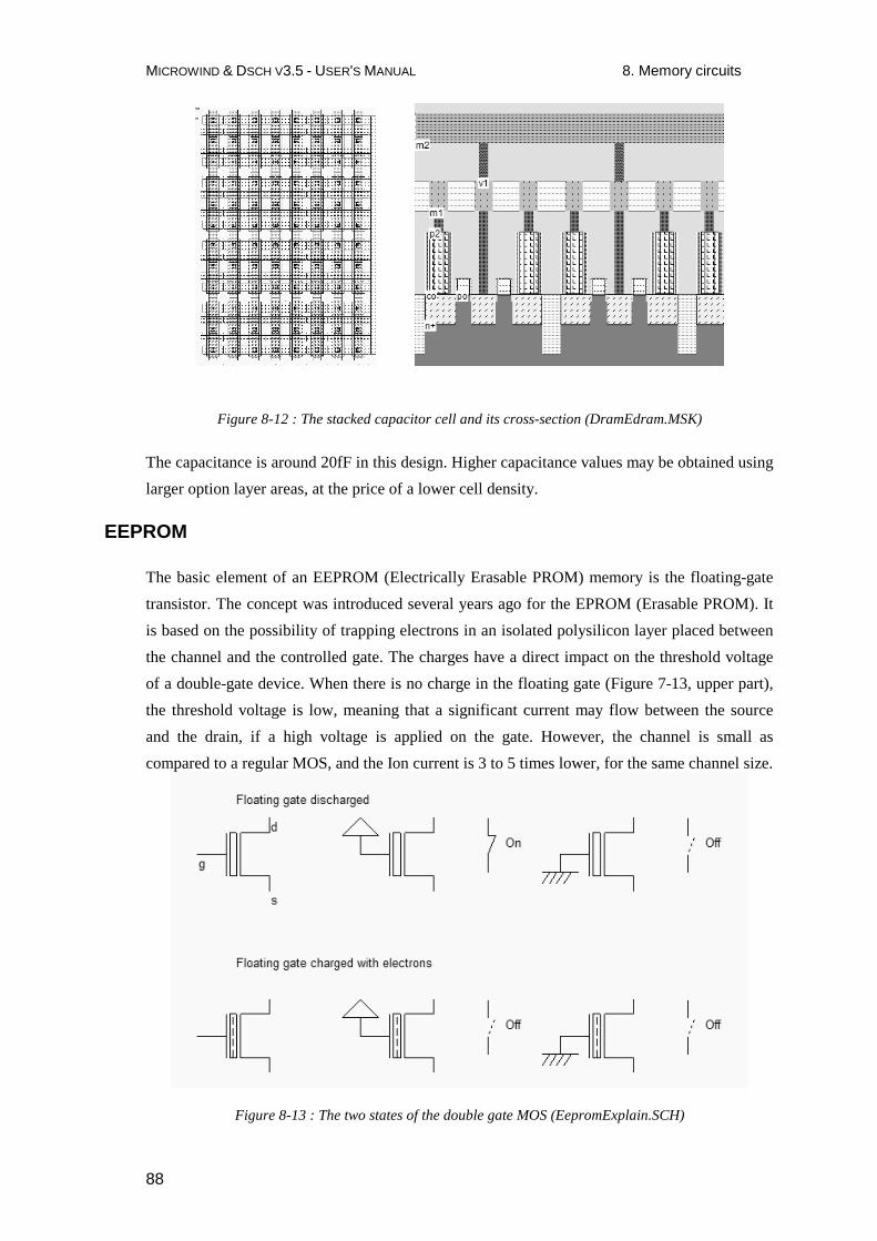
MICROWIND & DSCH V3.5 - USER'S MANUAL 8. Memory circuits
88
Figure 8-12 : The stacked capacitor cell and its cross-section (DramEdram.MSK)
The capacitance is around 20fF in this design. Higher capacitance values may be obtained using
larger option layer areas, at the price of a lower cell density.
EEPROM
The basic element of an EEPROM (Electrically Erasable PROM) memory is the floating-gate
transistor. The concept was introduced several years ago for the EPROM (Erasable PROM). It
is based on the possibility of trapping electrons in an isolated polysilicon layer placed between
the channel and the controlled gate. The charges have a direct impact on the threshold voltage
of a double-gate device. When there is no charge in the floating gate (Figure 7-13, upper part),
the threshold voltage is low, meaning that a significant current may flow between the source
and the drain, if a high voltage is applied on the gate. However, the channel is small as
compared to a regular MOS, and the Ion current is 3 to 5 times lower, for the same channel size.
Figure 8-13 : The two states of the double gate MOS (EepromExplain.SCH)

MICROWIND & DSCH V3.5 - USER'S MANUAL 8. Memory circuits
89
Poly2/metal contact
Poly2 on the top of poly
Floating poly underneath poly2
Floating poly gate
Ultra thin gate oxide
Controlled poly2 gate
Poly/Poly2 oxide
Figure 8-14 : The double gate MOS generated by Microwind (Eeprom.MSK)
When charges are trapped in the floating polysilicon layer (Figure 7-14, left), the threshold
voltage is high, almost no current flows through the device, independently of the gate value. As
a matter of fact, the electrons trapped in the floating gate prevent the creation of the channel by
repealing channel electrons. Data retention is a key feature of EEPROM, as it must be
guaranteed for a wide range of temperatures and operating conditions. Optimum electrical
properties of the ultra thin gate oxide and inter-gate oxide are critical for data retention. The
typical data retention of an EEPROM is 10 years.
The double gate MOS layout is shown in figure 7-14. The structure is very similar to the n-
channel MOS device, except for the supplementary poly2 layer on top of the polysilicon. The
lower polysilicon is unconnected, resulting in a floating node. Only the poly2 upper gate is
connected to a metal layer through a poly2/metal contact situated at the top. The cross-section
of figure 7-14 right reveals the stacked poly/poly2 structure, with a thin oxide in between.
Flash Memories
Flash memories are a variation of EEPROM memories. Flash arrays can be programmed
electrically bit-by-bit but can only be erased by blocks. Flash memories are based on a single
double poly MOS device, without any selection transistor (Figure 7-15). The immediate
consequence is a more simple design, which leads to a more compact memory array and more
dense structures. Flash memories are commonly used in micro-controllers for the storage of
application code, which gives the advantage of non volatile memories and the possibility of
reconfiguring and updating the code many times.
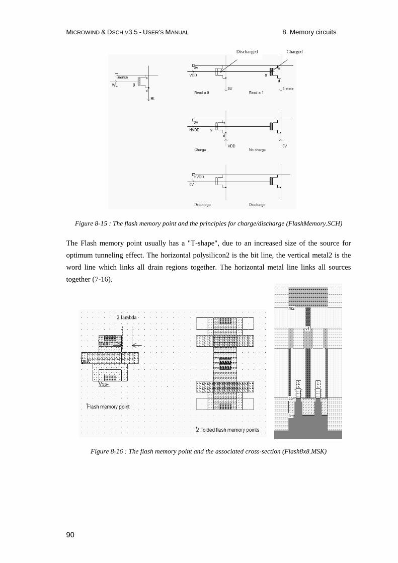
MICROWIND & DSCH V3.5 - USER'S MANUAL 8. Memory circuits
90
Discharged Charged
Figure 8-15 : The flash memory point and the principles for charge/discharge (FlashMemory.SCH)
The Flash memory point usually has a "T-shape", due to an increased size of the source for
optimum tunneling effect. The horizontal polysilicon2 is the bit line, the vertical metal2 is the
word line which links all drain regions together. The horizontal metal line links all sources
together (7-16).
2 lambda
Figure 8-16 : The flash memory point and the associated cross-section (Flash8x8.MSK)

MICROWIND & DSCH V3.5 - USER'S MANUAL 8. Memory circuits
91
Memory Interface
All inputs and outputs of the RAM are synchronized to the rise edge of the clock, and more
than one word can be read or written in sequence. The typical chronograms of a synchronous
RAM are shown in figure 7-17. The active edge of the clock is usually the rise edge. One read
cycle includes 3 active clock edges in the example shown in figure 7-17. The row address
selection is active at the first rise edge, followed by the column address selection. The data is
valid at the third fall edge of the system clock.
RowAddress
Row Address Selection (RAS)
Column Address Selection (CAS)
Write Enable (WE)
Data Out (Dout) Valid Dout
Read cycle (tRC)
Row Access Cycle tRAC
Column Access Cycle tCAC
(Read)
Active edge
System Clock (Clock)
Col
New cycle
Figure 8-17 : Synchronous RAM timing diagram
Added Features in the Full version
World of memories
Semiconductor memories are vital components in modern integrated circuits. The introductory part details the main families of memories.
Memories Compact memory cell obtained by sharing all possible contacts: the supply contact, the ground contact and the bit line contacts. Detailed information about ROM memories.
Double-gate MOS
The programming of a double-poly transistor involves the transfer of electrons from the source to the floating gate through the thin oxide. Details are provided on the programming and charge removal.
Ferroelectric RAM
FRAM memories are the most advanced of the Flash memory challengers. The FRAM memory point is based on a two-state ferroelectric insulator. A complete description and simulation of the FRAM is proposed.
Interfacing Some information is provided about the Double data Rate memories, which involve both the rise and fall edge of the clock.

MICROWIND & DSCH V3.5 - USER'S MANUAL 9. Analog Cells
92
This chapter deals with analog basic cells, from the simple resistor and capacitor to the operational
amplifier. A very complete description of analog cells may be found in [Razavi], and details on analog
layout techniques may be found in [Hastings].
Resistor
An area-efficient resistor available in CMOS process downto 65-nm consists of a strip of polysilicon. The
resistance between s1 and s2 is usually counted in a very convenient unit called "ohm per square", noted
Ω/ . The default value polysilicon resistance per square is 10Ω, which is quite small, but rises to 200Ω if
the salicide material is removed (Figure 8-1).
polysilicon
1 2 … 7
One square accounts for 10Ω
Metal/poly contact
S1 S2
7x10Ω= 70Ω
Option layer which removes the salicide
1 2 … 7
One square accounts for 200Ω
S1 S2
7x200Ω= 1400Ω
S1 S2
S1 S2
Figure 9-1 : The polysilicon resistance with unsalicide option
As the default technology in Microwind 3.5 is 45-nm, where polysilicon has been replaced by metal, use
File → Select Foundry and choose “cmos65nm.RUL” to reconfigure the software to a CMOS process using
polysilicon as gate material. In the cross-section shown in figure 8-2, the salicide material deposited on the
upper interface between the polysilicon layer and the oxide creates a metal path for current that reduces the
resistance dramatically. Notice the shallow trench isolation and surrounding oxide that isolate the resistor
from the substrate and other conductors, enabling very high voltage biasing (up to 100V). However, the
oxide is a poor thermal conductor which limits the power dissipation of the polysilicon resistor.
The salicide is part of the default process, and is present at the surface of all polysilicon areas. However, it
can be removed thank to an option layer programmed by a double click in the option layer box, and a tick at
"Remove Salicide". In the example shown in figure 8-3, the default resistance is 76 Ω, and the unsalicide
resistance rises to 760 Ω.
9 Analog Cells
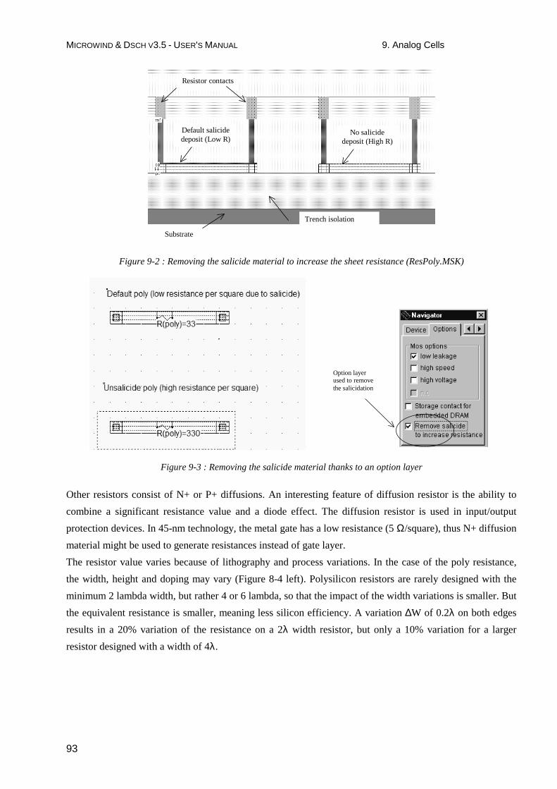
MICROWIND & DSCH V3.5 - USER'S MANUAL 9. Analog Cells
93
Trench isolation
Substrate
Default salicidedeposit (Low R)
No salicidedeposit (High R)
Resistor contacts
Figure 9-2 : Removing the salicide material to increase the sheet resistance (ResPoly.MSK)
Option layer used to remove the salicidation
Figure 9-3 : Removing the salicide material thanks to an option layer
Other resistors consist of N+ or P+ diffusions. An interesting feature of diffusion resistor is the ability to
combine a significant resistance value and a diode effect. The diffusion resistor is used in input/output
protection devices. In 45-nm technology, the metal gate has a low resistance (5 Ω/square), thus N+ diffusion
material might be used to generate resistances instead of gate layer.
The resistor value varies because of lithography and process variations. In the case of the poly resistance,
the width, height and doping may vary (Figure 8-4 left). Polysilicon resistors are rarely designed with the
minimum 2 lambda width, but rather 4 or 6 lambda, so that the impact of the width variations is smaller. But
the equivalent resistance is smaller, meaning less silicon efficiency. A variation ∆W of 0.2λ on both edges
results in a 20% variation of the resistance on a 2λ width resistor, but only a 10% variation for a larger
resistor designed with a width of 4λ.

MICROWIND & DSCH V3.5 - USER'S MANUAL 9. Analog Cells
94
∆W
∆h
∆N (doping)
∆W=0.2λ ∆W=0.2λ
20% variation 10% variation
oxide
Poly
2λ 4λ
Figure 9-4 : Resistance variations with the process
In CMOS 45-nm technology, the gate material features a low resistivity as it is based on metal materials
(See section 1).
Capacitor
Capacitors are used in analog design to build filters, compensation, decoupling, etc.. Ideally, the value of the
capacitor should not depend on the bias conditions, so that the filtering effect would be situated at constant
frequencies.
Diodes in reverse mode exhibit a capacitor behavior, however, the capacitance value is strongly dependent
on the bias conditions. A simple N+ diffusion on a P-substrate is a NP diode, which may be considered as a
capacitor as long as the N+ region is polarized at a voltage higher than the P-substrate voltage which is
usually the case as the substrate is grounded (0V). In 0.12µm, the capacitance is around 300aF/µm2 (1 atto-
Farad is equal to 10-18 Farad).
The typical variation of the capacitance with the diffusion voltage VN is given in figure 8-6. The capacitance
per µm2 provided in the electrical rules is a rude approximation of the capacitance variation. A large voltage
difference between VN and the substrate result in a thick zone with empty charges, which corresponds to a
thick insulator, and consequently to a small capacitance. When VN is lowered, the zone with empty charges
is reduced, and the capacitance increases. If VN goes lower than the substrate voltage, the diode starts to
conduct.
P- N+
VPN
VPN<VT
Very small current
VPN>VT
Large current
VT
iPN
VPN
Figure 9-5 : The diffusion over substrate as a non-linear capacitor (Capa.MSK)
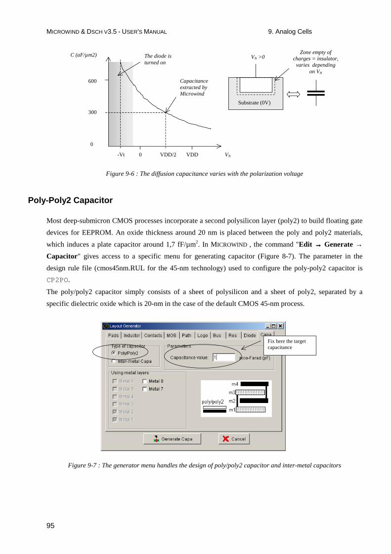
MICROWIND & DSCH V3.5 - USER'S MANUAL 9. Analog Cells
95
Capacitance extracted by Microwind
VN VDD/2 0 -Vt
C (aF/µm2)
300
600
0
VDD
The diode is turned on
VN >0
Substrate (0V)
Zone empty of charges = insulator, varies depending
on VN
Figure 9-6 : The diffusion capacitance varies with the polarization voltage
Poly-Poly2 Capacitor
Most deep-submicron CMOS processes incorporate a second polysilicon layer (poly2) to build floating gate
devices for EEPROM. An oxide thickness around 20 nm is placed between the poly and poly2 materials,
which induces a plate capacitor around 1,7 fF/µm2. In MICROWIND , the command "Edit →→→→ Generate →
Capacitor" gives access to a specific menu for generating capacitor (Figure 8-7). The parameter in the
design rule file (cmos45nm.RUL for the 45-nm technology) used to configure the poly-poly2 capacitor is
CP2PO.
The poly/poly2 capacitor simply consists of a sheet of polysilicon and a sheet of poly2, separated by a
specific dielectric oxide which is 20-nm in the case of the default CMOS 45-nm process.
Fix here the target capacitance
Figure 9-7 : The generator menu handles the design of poly/poly2 capacitor and inter-metal capacitors

MICROWIND & DSCH V3.5 - USER'S MANUAL 9. Analog Cells
96
Diode-connected MOS
The schematic diagram of the diode-connected MOS is proposed in figure 8-8. This circuit features a high
resistance within a small silicon area. The key idea is to build a permanent connection between the drain
and the gate. Most of the time, the source is connected to ground in the case of n-channel MOS, and to VDD
in the case of p-channel MOS.
Figure 9-8 : Schematic diagram of the MOS connected as a diode (MosRes.SCH)
To create the diode-connected MOS, the easiest way is to use the MOS generator. Enter a large length and a
small width, for example W=0.14µm and L=1.4µm. This sizing corresponds to a long channel, featuring a
very high equivalent resistance. Add a poly/metal contact and connect the gate to one diffusion. Add a clock
on that node. Add a VSS property to the other diffusion. The layout result is shown in figure 8-9.
Now, click Simulation on Layout. In a small window, the MOS characteristics are drawn, with the
functional point drawn as a color dot (Figure 8-10). It can be seen that the I/V characteristics correspond to
a diode. The resistance is the invert value of the slope in the Id/Vd characteristics. For Vds larger than 0.6V,
the resistance is almost constant. As the current Ids increases of 10µA in 0.4V, the resistance can be
estimated around 40KΩ. A more precise evaluation is performed by MICROWIND if you draw the slope
manually. At the bottom of the screen, the equivalent resistance appears, together with the voltage and
current.
Figure 9-9 : Schematic diagram of the MOS connected as a diode (ResMos.MSK)

MICROWIND & DSCH V3.5 - USER'S MANUAL 9. Analog Cells
97
The slope is equal to 1/R
As Vd=Vg, Ids follows this unique
curve
Draw the slope with the mouse to display the equivalent R
Figure 9-10 : Using the Simulation on Layout to follow the characteristics of the diode-connected MOS (ResMos.MSK)
In summary, the MOS connected as a diode is a capacitance for Vgs<Vt, a high resistance when Vgs is
higher than the threshold voltage Vt. The resistance obtained using such a circuit can easily reach 100KΩ in
a very small silicon area.
Voltage Reference
The voltage reference is usually derived from a voltage divider made from resistance. The output voltage
Vref is defined by equation 8-1.
DDPN
Nref V
RR
RV
+= (Eq. 8-1)
with
VDD=power supply voltage (1.0 V in 65-nm)
RN=equivalent resistance of the n-channel MOS (Ω)
RP=equivalent resistance of the p-channel MOS (Ω)
Notice that two n-MOS or two p-MOS properly connected feature the same function. P-MOS devices offer
higher resistance due to lower mobility, compared to n-channel MOS. Four voltage reference designs are
shown in figure 8-11. The most common design uses one p-channel MOS and one n-channel MOS
connected as diodes.

MICROWIND & DSCH V3.5 - USER'S MANUAL 9. Analog Cells
98
Figure 9-11 : Voltage reference using PMOS and NMOS devices as large resistance
Figure 9-12 : Voltage reference circuits (a) with one nMOS and one pMOS (b) with two pMOS (Vref.MSK)
The alternative solutions consist in using two n-channel MOS devices only (Left lower part of figure 8-12),
or their opposite built from p-channel devices only. Not only one reference voltage may be created, but also
three, as shown in the right part of the figure, which use four n-channel MOS devices connected as diodes.
Amplifier
The goal of the amplifier is to multiply by a significant factor the amplitude of a sinusoidal voltage input
Vin, and deliver the amplified sinusoidal output Vout on a load. The single stage amplifier may consist of a
MOS device (we choose here a n-channel MOS) and a load. The load can be a resistance or an inductance.
In the circuit, we use a resistance made with a p-channel MOS device with gate and drain connected (Figure
8-13). The pMOS which replaces the passive load is called an active resistance.

MICROWIND & DSCH V3.5 - USER'S MANUAL 9. Analog Cells
99
Figure 9-13 : Single stage amplifier design with MOS devices (AmpliSingle.SCH)
VIN
VOUT
vin
vout The gain (slope)
is high in this region
Input voltage (V)
Output voltage (V)
Gain VIN +vin VOUT +vout
Most interesting
zone
VIN_low VIN_high
Figure 9-14 : The amplifier has a high gain in a certain input range, where a small input signal vin is amplified to a
large signal vout.
The single stage amplifier characteristics between Vin and Vout have a general shape shown in figure 8-14.
The most interesting zone corresponds to the input voltage range where the transfer function has a linear
shape, that is between VIN_low and VIN_high. Outside this voltage range, the behavior of the circuit does
not correspond anymore to an amplifier. If we add a small sinusoidal input vin to VIN, a small variation of
current ids is added to the static current IDS, which induces a variation vout of the output voltage VOUT. The
link between the variation of current ids and the variation of voltage vin can be approximated by equation 8-2.
gsmds vgi = (Equ. 8-2)

MICROWIND & DSCH V3.5 - USER'S MANUAL 9. Analog Cells
100
Figure 9-15 : Single stage amplifier layout with a pMOS as a load resistor (AmpliSingle.MSK)
In figure 8-15, a nMOS device with large width and minimum length is connected to a high resistance
pMOS load. A 50 mV sinusoidal input (vin) is superimposed to the static offset 0.5 V (VIN). What we expect
is a 500 mV sinusoidal wave (vout) with a certain DC offset (VOUT).
What we need now is to find the characteristics Vout/Vin in order to tune the offset voltage VIN. In the
simulation window, click Voltage vs voltage” and More, to compute the static response of the amplifier
(Figure 8-16). The range of voltage input that exhibits a correct gain appears clearly. For VIn higher than 0.1
V and lower than 0.25 V, the output gain is around 6. Therefore, an optimum offset value could be 0.15 V.
Change the parameter Offset of the input sinusoidal wave to place the input voltage in the correct
polarization and verify the amplification of the output signal according to DC predictions. By increasing the
Vin frequency, you may observe the cut-off frequency of the amplifier (Fig. 8-17).
Linear amplification (Gain maximum
around 6.0)
Valid input voltage range
Figure 9-16 : Single stage amplifier static response showing the valid input voltage range (AmpliSingle.MSK)

MICROWIND & DSCH V3.5 - USER'S MANUAL 9. Analog Cells
101
Offset 150 mV
High gain at low frequency
Gain reduced due to load capacitance
Figure 9-17 : Simulation with Vin input offset tuned to optimum gain (AmpliSingle.MSK)
Simple Differential Amplifier
The goal of the differential amplifier is to compare two analog signals, and to amplify their difference. The
differential amplifier formulation is reported below (Equation 8-3). Usually, the gain K is high, ranging
from 10 to 1000. The consequence is that the differential amplifier output saturates very rapidly, because of
the supply voltage limits.
( )VmVpKVout −= (Equ. 8-3)
The schematic diagram of a basic differential amplifier is proposed in figure 8-18. An nMOS device has
been inserted between the differential pair and the ground to improve the gain. The gate voltage Vbias
controls the amount of current that can flow on the two branches. This pass transistor permits the
differential pair to operate at lower Vds, which means better analog performances and less saturation effects.
The best way to measure the input range is to connect the differential amplifier as a follower, that is Vout
connect to Vm. The Vm property is simply removed, and a contact poly/metal is added at the appropriate
place to build the bridge between Vout and Vm. A slow ramp is applied on the input Vin and the result is
observed on the output. We use again the « Voltage vs. Voltage » to draw the static characteristics of the
follower.

MICROWIND & DSCH V3.5 - USER'S MANUAL 9. Analog Cells
102
Figure 9-18 : An improved differential amplifier (AmpliDiff.SCH)
The simulation of the circuit is performed here using the CMOS 45-nm technology. You may also simulate
the circuit in other technologies using the command File →→→→ Select Foundry. As can be seen from the
resulting simulation reported in figure 8-19, a low Vbias features a larger voltage range, specifically at high
voltage values. The follower works properly starting 0.2 V, independently of the Vbias value (Fig. 8-20). A
high Vbias leads to a slightly faster response, but reduces the input range and consumes more power as the
associated nMOS transistor drives an important current. The voltage Vbias is often fixed to a value a little
higher than the threshold voltage Vtn. This corresponds to a good compromise between switching speed and
input range.
PMOS current mirrorwith large length
nMOS differentialpair with large length
Voltage control of theglobal current consumption
OpAmp connected asa follower
Label used to force BSIM4model at simulation, rather thanModel 3
Figure 9-19 : The layout corresponding to the improved differential amplifier (AmpliDiffFollow.MSK)
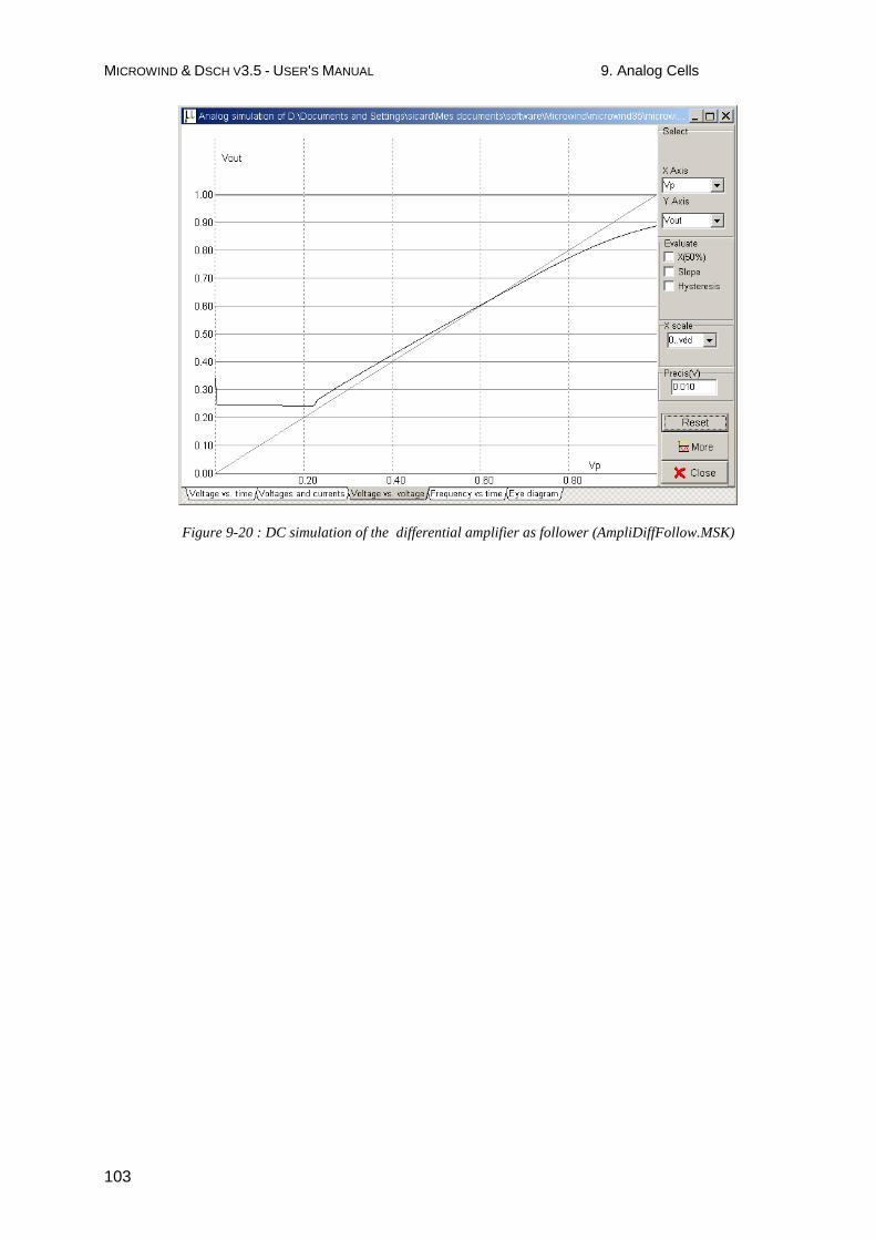
MICROWIND & DSCH V3.5 - USER'S MANUAL 9. Analog Cells
103
Figure 9-20 : DC simulation of the differential amplifier as follower (AmpliDiffFollow.MSK)

MICROWIND & DSCH V3.5 - USER'S MANUAL 9. Analog Cells
104
Added Features in the Full version
Amplifiers The push-pull amplifier is built using a voltage comparator and a power output stage. Its
schematic diagram and performances are detailed.
Improved layout techniques
A set of design techniques can improve the current mirror behavior: MOS orientation, channel length modulation effects, dummy devices, MOS matching.
Resistor There exist efficient techniques to reduce the resistance variations within the same chip. Layout techniques which minimize the effects of process variations are presented.
Capacitor The multiplication of metal layers create lateral and vertical capacitance effects of rising importance. The spared silicon area in upper metal layers may be used for small size capacitance. The implementation of these capacitor is described.
Current Mirror The current mirror is one of the most useful basic blocs in analog design. It is primarily used to copy currents. The principles and behavior of current mirrors are given in the full version. The cascode current mirror is also presented, which has several advantages over the simple current mirror.

MICROWIND & DSCH V3.5 - USER'S MANUAL 9.Radio-frequency Circuits
105
On-Chip Inductors
Inductors are commonly used for filtering, amplifying, or for creating resonant circuits used in
radio-frequency applications. The inductance symbol in DSCH and MICROWIND is as follows
(Figure 9-1).
Figure 10-1 : The inductance symbol
The quality factor Q is a very important metric to quantify the resonance effect. A high quality
factor Q means low parasitic effects compared to the desired inductance effect. The formulation
of the quality factor is not as easy as it could appear. An extensive discussion about the
formulation of Q depending on the coil model is given in [Lee]. We consider the coil as a serial
inductor L1, a parasitic serial resistor R1, and two parasitic capacitors C1 and C2 to the
ground, as shown in figure 9-2. Consequently, the Q factor is approximately given by equation
9-1.
1
)21(
1
R
CC
L
Q+
= (Equ. 9-1)
The inductor can be generated automatically by MICROWIND using the command Edit →→→→
Generate →→→→ Inductor . The inductance value appears at the bottom of the window, as well as
the parasitic resistance and the resulting quality factor Q.
A
B
C
Figure 10-2 : The equivalent model of the 12nH default coil and the approximation of the quality factor
Q
10 Radio Frequency Circuits

MICROWIND & DSCH V3.5 - USER'S MANUAL 9.Radio-frequency Circuits
106
Near end of the coil
Far end of the coil
Virtual symbol forthe serial resistor
Virtual symbol forthe serial inductor
A
B
C
Figure 10-3 : The inductor generated by default (inductor12nH.MSK)
Using the default parameters, the coil inductance approaches 12 nH, with a quality factor of
Q=1.15. The corresponding layout is shown in figure 9-3. Notice the virtual inductance (L1)
and resistance (R1) symbols placed in the layout. The serial inductor is placed between A and B
and a serial resistance between B and C. If these symbols were omitted, the whole inductor
would be considered as a single electrical node.
The coil can be considered as a RLC resonant circuit. At very low frequencies, the inductor is a
short circuit, and the capacitor is an open circuit (Figure 9-4 left). This means that the voltage at
node C is almost equal to A, if no load is connected to node C, as almost no current flows
through R1. At very high frequencies, the inductor is an open circuit, the capacitor a short
circuit (Figure 9-4 right). Consequently, the link between C and A tends towards an open
circuit.
Figure 10-4 : The behavior of a RLC circuit at low and high frequencies (Inductor.SCH)
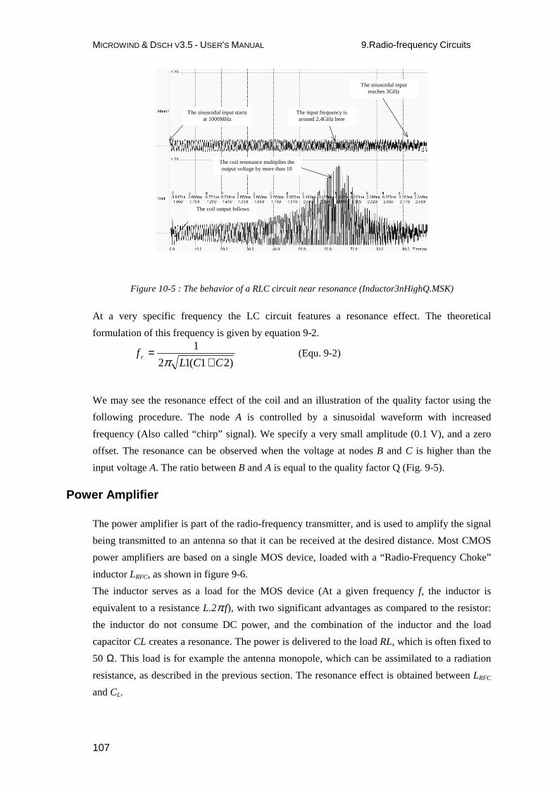
MICROWIND & DSCH V3.5 - USER'S MANUAL 9.Radio-frequency Circuits
107
The sinusoidal input starts at 1000MHz
The coil output follows
The coil resonance multiplies the output voltage by more than 10
The sinusoidal input reaches 3GHz
The input frequency is around 2.4GHz here
Figure 10-5 : The behavior of a RLC circuit near resonance (Inductor3nHighQ.MSK)
At a very specific frequency the LC circuit features a resonance effect. The theoretical
formulation of this frequency is given by equation 9-2.
)21(12
1
CCLf r +
=π
(Equ. 9-2)
We may see the resonance effect of the coil and an illustration of the quality factor using the
following procedure. The node A is controlled by a sinusoidal waveform with increased
frequency (Also called “chirp” signal). We specify a very small amplitude (0.1 V), and a zero
offset. The resonance can be observed when the voltage at nodes B and C is higher than the
input voltage A. The ratio between B and A is equal to the quality factor Q (Fig. 9-5).
Power Amplifier
The power amplifier is part of the radio-frequency transmitter, and is used to amplify the signal
being transmitted to an antenna so that it can be received at the desired distance. Most CMOS
power amplifiers are based on a single MOS device, loaded with a “Radio-Frequency Choke”
inductor LRFC, as shown in figure 9-6.
The inductor serves as a load for the MOS device (At a given frequency f, the inductor is
equivalent to a resistance L.2π.f), with two significant advantages as compared to the resistor:
the inductor do not consume DC power, and the combination of the inductor and the load
capacitor CL creates a resonance. The power is delivered to the load RL, which is often fixed to
50 Ω. This load is for example the antenna monopole, which can be assimilated to a radiation
resistance, as described in the previous section. The resonance effect is obtained between LRFC
and CL.

MICROWIND & DSCH V3.5 - USER'S MANUAL 9.Radio-frequency Circuits
108
Model of the antenna
On-chip inductor
On-chip capacitor
Oscillation of Vout
Input signal VrfIn
Figure 10-6 : The basic diagram of a power amplifier (PowerAmp.SCH)
An example of powerful MOS device is shown in figure 9-7. The maximum current is close to
10 mA in 45-nm technology. A convenient way to generate the polarization ring consists in
using the Path generator command, and selection the option Metal and p-diffusion. Then draw
the location for the polarization contacts in order to complete the ring.
The distinction between class A,B,AB, etc.. amplifiers is mainly given with the polarization of
the input signal. A Class A amplifier is polarized in such a way that the transistor is always
conducting. The MOS device operates almost linearly.
Figure 10-7 : The layout of the power MOS also includes a polarization ring, and the contacts to metal2
connections to VRF_in and VOut (PowerAmplifier.MSK)

MICROWIND & DSCH V3.5 - USER'S MANUAL 9.Radio-frequency Circuits
109
Figure 10-8 : The class A amplifier has a sinusoidal input (PowerAmplifierClassA.MSK)
The sinusoidal input offset is 0.7 V, the amplitude is 0.4V. The power MOS functional point
trajectory is plotted in figure 9-8, and is obtained using the command Simulate on Layout. We
see the evolution of the functional point with the voltage parameters: as Vgs varies from 0.3 V
to 1.1 V, Ids fluctuates between 10 mA and 30 mA. The MOS device is always conducting,
which corresponds to class A amplifiers.
Oscillator
The role of oscillators is to create a periodic logic or analog signal with a stable and predictable
frequency. Oscillators are required to generate the carrying signals for radio frequency
transmission, but also for the main clocks of processors. The ring oscillator is a very simple
oscillator circuit, based on the switching delay existing between the input and output of an
inverter. If we connect an odd chain of inverters, we obtain a natural oscillation, with a period
which corresponds roughly to the number of elementary delays per gate. The fastest oscillation
is obtained with 3 inverters (One single inverter connected to itself does not oscillate). The
usual implementation consists in a series of five up to one hundred chained inverters (Figure 9-
9).

MICROWIND & DSCH V3.5 - USER'S MANUAL 9.Radio-frequency Circuits
110
Figure 10-9 : A ring oscillator is based on an odd number of inverters (Inv3.SCH)
The main problem of this type of oscillators is the very strong dependence of the output
frequency on virtually all process parameters and operating conditions. This means that any
supply fluctuation has a significant impact on the oscillator frequency.
The LC oscillator proposed below is not based on the logic delay, as with the ring oscillator,
but on the resonant effect of a passive inductor and capacitor circuit. In the schematic diagram
of figure 9-10, the inductor L1 resonates with the capacitor C1 connected to S1 combined with
C2 connected to S2.
The layout implementation is performed using a 3 nH virtual inductor and two 1 pF capacitor.
The large width of active devices to ensure a sufficient current to charge and discharge the huge
capacitance of the output node at the desired frequency.
Figure 10-10 : A differential oscillator using an inductor and companion capacitor (OscillatorDiff.SCH)

MICROWIND & DSCH V3.5 - USER'S MANUAL 9.Radio-frequency Circuits
111
DC current is established Oscillation
starts
Permanent regime
Figure 10-11 : Simulation of the differential oscillator (OscillatorDiff.MSK)
Using virtual capacitors instead of on-chip physical coils is recommended during the
development phase. It allows an easy tuning of the inductor and capacitor elements in order to
achieve the correct behavior. Once the circuit has been validated, the L and C symbols can be
replaced by physical components. The time-domain simulation (Figure 9-11) shows a warm-up
period around 1ns where the DC supply rises to its nominal value, and where the oscillator
effect reaches a permanent state after some nano-seconds.
The Fourier transform of the output s1 reveals a main sinusoidal contribution at f0 =3.725 GHz
as expected, and some harmonics at 2 x f0 and 3 x f0 (Figure 9-12). The remarkable property of
this circuit is its ability to remain in a stable frequency even if we change the supply voltage or
the temperature, which features a significant improvement as compared to the ring oscillator.
Furthermore, the variations of the MOS model parameters have almost no effect on the
frequency.
0.9V, 100°C
1.2V, 27°C
2.f0f0 3.f0
Figure 10-12 : The frequency spectrum of the oscillator (OscillatorDiff.MSK)

MICROWIND & DSCH V3.5 - USER'S MANUAL 9.Radio-frequency Circuits
112
Analog to digital and digital to analog converters
The analog to digital converters (ADC) and digital to analog converters (DAC) are the main
links between the analog signals and the digital world of signal processing. The ADC and DAC
viewed as black boxes are shown in figure 9-13. On the right side, the ADC takes an analog
input signal Vin and converts it to a digital output signal A. The digital signal A is a binary
coded representation of the analog signal using N bits: AN-1 … A0. The maximum number of
codes for N bits is 2N. The digital signal is usually treated by a microprocessor unit (MPU) or
by a specific digital signal processor (DSP) before being restituted as an output B. Then, the
DAC, which has the opposite function compared to the ADC, converts the digital signal to the
final analog output signal Vout.
V IN
t
ADC
A0 A1
AN-1 DAC
MPU DSP
B0 B1
BN-1
VOUT
t
Figure 10-13 : Basic principle of N bits analog to digital and digital to analog converters.
The most basic DAC is based on a resistance ladder. This type of DAC consists of a simple
resistor string of 2N identical resistors, and a binary switch array whose inputs are a binary
word. The analog output is the voltage division of the resistors flowing via pass switches
(figure 9-14).
In the implementation shown in figure 9-15, the resistance ladder includes 8 identical resistors,
which generate 8 reference voltage equally distributed between the ground voltage and Vdac.
The digital-analog converter uses the three-bit input B (B[2],B[1],B[0] ) to control the
transmission gate network which selects one of the voltage references (A portion of Vdac)
which is then transferred to the output Vout. A long path of polysilicon between VDD and VSS
may give intermediate voltage references required for the DAC circuit.
B[2] B[1] B[0] Vout* Analog output Vout* (V) with
Vdac=1.0V 0 0 0 0/8 Vdac 0.0 0 0 1 1/8 Vdac 0.125 0 1 0 2/8 Vdac 0.25 0 1 1 3/8 Vdac 0.375 1 0 0 4/8 Vdac 0.5 1 0 1 5/8 Vdac 0.625 1 1 0 6/8 Vdac 0.75 1 1 1 7/8 Vdac 0.875
Figure 10-14 : The specifications of a 3-bit digital-to-analog converter

MICROWIND & DSCH V3.5 - USER'S MANUAL 9.Radio-frequency Circuits
113
Figure 10-15 : The sheet resistance is increased by removing the salicide deposit, thanks to an option
layer, for technologies above 65-nm (DAC.MSK)
The simulation of the R ladder DAC (Figure 9-16) shows a regular increase of the output
voltage Vout with the input B[0]..B[2] from “000” (0 V) to “111” (nearly 1.0 V). Each input
change provokes a capacitance network charge and discharge. The analog level Vout increases
regularly with increasing digit input B. The converter is monotonic.
Figure 10-16 : Simulation of the digital-analog converter (DAC.MSK).
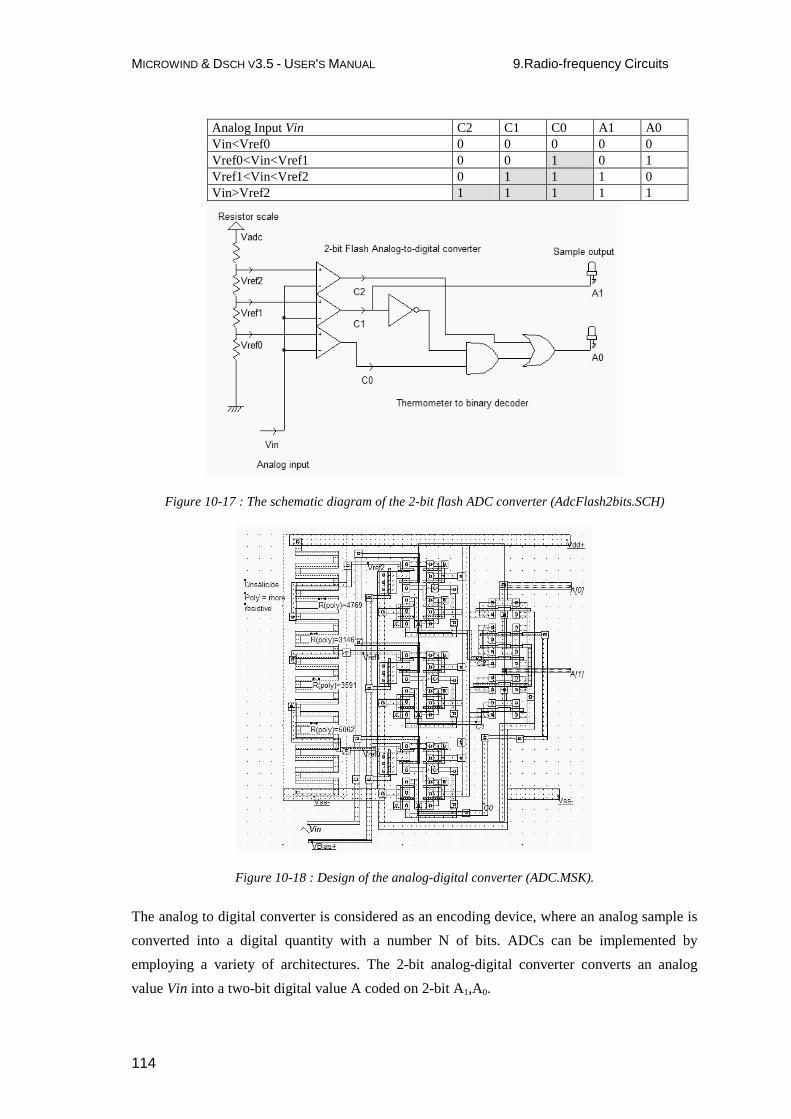
MICROWIND & DSCH V3.5 - USER'S MANUAL 9.Radio-frequency Circuits
114
Analog Input Vin C2 C1 C0 A1 A0 Vin<Vref0 0 0 0 0 0 Vref0<Vin<Vref1 0 0 1 0 1 Vref1<Vin<Vref2 0 1 1 1 0 Vin>Vref2 1 1 1 1 1
Figure 10-17 : The schematic diagram of the 2-bit flash ADC converter (AdcFlash2bits.SCH)
Figure 10-18 : Design of the analog-digital converter (ADC.MSK).
The analog to digital converter is considered as an encoding device, where an analog sample is
converted into a digital quantity with a number N of bits. ADCs can be implemented by
employing a variety of architectures. The 2-bit analog-digital converter converts an analog
value Vin into a two-bit digital value A coded on 2-bit A1,A0.
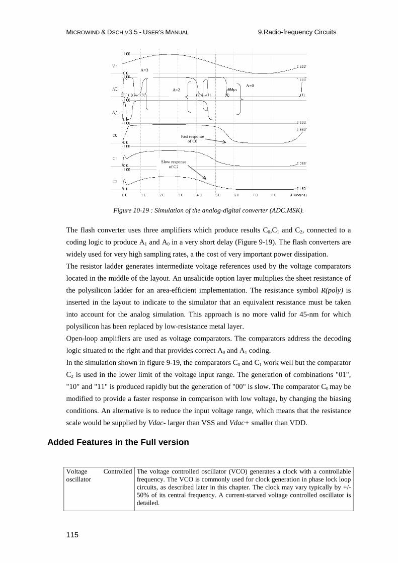
MICROWIND & DSCH V3.5 - USER'S MANUAL 9.Radio-frequency Circuits
115
A=3
A=2 A=0
Slow response of C2
Fast response of C0
Figure 10-19 : Simulation of the analog-digital converter (ADC.MSK).
The flash converter uses three amplifiers which produce results C0,C1 and C2, connected to a
coding logic to produce A1 and A0 in a very short delay (Figure 9-19). The flash converters are
widely used for very high sampling rates, a the cost of very important power dissipation.
The resistor ladder generates intermediate voltage references used by the voltage comparators
located in the middle of the layout. An unsalicide option layer multiplies the sheet resistance of
the polysilicon ladder for an area-efficient implementation. The resistance symbol R(poly) is
inserted in the layout to indicate to the simulator that an equivalent resistance must be taken
into account for the analog simulation. This approach is no more valid for 45-nm for which
polysilicon has been replaced by low-resistance metal layer.
Open-loop amplifiers are used as voltage comparators. The comparators address the decoding
logic situated to the right and that provides correct A0 and A1 coding.
In the simulation shown in figure 9-19, the comparators C0 and C1 work well but the comparator
C2 is used in the lower limit of the voltage input range. The generation of combinations "01",
"10" and "11" is produced rapidly but the generation of "00" is slow. The comparator C0 may be
modified to provide a faster response in comparison with low voltage, by changing the biasing
conditions. An alternative is to reduce the input voltage range, which means that the resistance
scale would be supplied by Vdac- larger than VSS and Vdac+ smaller than VDD.
Added Features in the Full version
Voltage Controlled oscillator
The voltage controlled oscillator (VCO) generates a clock with a controllable frequency. The VCO is commonly used for clock generation in phase lock loop circuits, as described later in this chapter. The clock may vary typically by +/-50% of its central frequency. A current-starved voltage controlled oscillator is detailed.

MICROWIND & DSCH V3.5 - USER'S MANUAL 9.Radio-frequency Circuits
116
Gilbert mixer The Gilbert mixer is used to shift the frequency of an input signal Vin to a high frequency. The Gilbert cell consists of only six transistors, and performs a high quality multiplication of the sinusoidal waves. The schematic diagram and the physical implementation are described in the full version.
Phase-Lock-Loop Each basic component of the PLL (Phase comparator, filter, VCO) and the design issues are described, supported by a large set of simulations.
Digital to analog converter
The R-2R ladder consists of a network of resistors alternating between R and 2R. For a N bits DAC, only N cells based on 2 resistors R and 2R in series are required. The 4-bit and 8-bit implementation of this circuit are described.
Sample and Hold The sample-and-hold main function is to capture the signal value at a given instant and hold it until the ADC has processed the information The principles and parasitic effects of the circuit are described.
Analog to digital converter
Successive approach analog to digital converter.

MICROWIND & DSCH V3.5 - USER'S MANUAL 11. I/O Interfacing
117
This chapter is dedicated to the interfacing between the integrated circuit and the external word.
After a brief justification of the power supply decrease, the input/output pads used to import
and export signals are dealt with. Then, the input pad protections against electrostatic discharge
and voltage overstress are described. The design of output buffers is also presented, with focus
on current drive.
The Bonding Pad
The bonding pad is the interface between the integrated circuit die and the package. The pad
has a very large surface (Almost giant compared to the size of logic cells) because it is the place
where the connection wire is attached to build the electrical link to the outside word. The pad is
approximately 50 µm x 50 µm. The basic design rules for the pad are shown in figure 10-1.
Rp01 (~50µm)
Rp02 (~50µm)
Rp03
Rp05
Rp04
Rp03
Rp04
Active area
Passivation
Passivation opening
Last metal
Metal 1
Passivation opening limits
Metal 1..8 area Via 1..5 area
Via 1
Soldier ball
Figure 11-1 : The bonding pad design rules
The cross-section shown in figure 10-2 gives an illustration of the passivation opening and
associated design rule Rp04 on top of the metal and via stack. The thick oxide used for
passivation is removed so that a bonding wire or a bonding ball can be connected by melting to
the package. The pad can be generated by MICROWIND using the command Edit →→→→ Generate
→→→→ I/O pads. The menu gives access to a single pad, with a default size given by the technology
(around 50µm in this case), or to a complete pad rind, as detailed later.
11 Input/Output Interfacing

MICROWIND & DSCH V3.5 - USER'S MANUAL 11. I/O Interfacing
118
The Pad ring
The pad ring consists of several pads on each of the four sides of the integrated circuit, to
interface with the outside world. The default menu for an automatic generation of a pad ring is
shown in figure 10-2. The proposed architecture is based on 5 pads on each side, meaning a
total of 20 pads.
Core area
5 pads south
5 pads north
5 pads west 5 pads
east
Limit of the die
Inner supply ring (Usually VDD)
Outer supply ring (Usually VSS)
Figure 11-2 : The menu for generating the pad ring and the corresponding architecture
The supply rails
The supply voltage may be 5 V, 3.3 V, 2.5 V, 1.8 V or 1.2 V as listed in the menu shown in
figure 10-2. Most designs in 45-nm use 1.0 V for the internal core supply and 2.5V for the
interfacing. This is because the logic circuits of the core operate at low voltage to reduce power
consumption, and the I/O structures operate at high voltage for external compatibility and
higher immunity to external perturbations. Usually, an on-chip voltage regulator converts the
high voltage into an internal low voltage.
A metal wire cannot drive an unlimited amount of current. When the average current density is
higher than 2.109 A/m2 [Hastings], the grains of the polycrystalline aluminum interconnect start
to migrate (The phenomenon is called electro migration) and the conductor ultimately melts. To
handle very high current density, the supply metal lines must be enlarged. A typical rule of
thumb is 2 mA/µm width for aluminum supply lines and 5 mA/µm for copper, which means
that a copper interconnect is superior to aluminum in sustaining large currents.
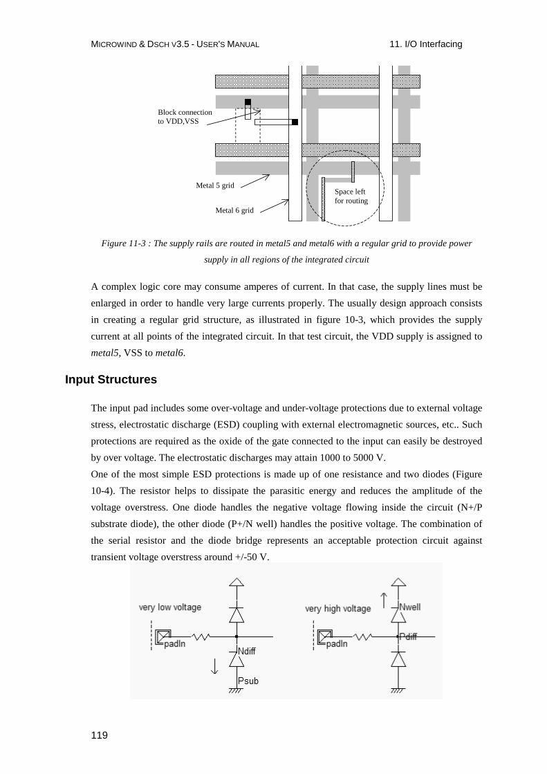
MICROWIND & DSCH V3.5 - USER'S MANUAL 11. I/O Interfacing
119
Metal 6 grid
Metal 5 grid
Block connection to VDD,VSS
Space left for routing
Figure 11-3 : The supply rails are routed in metal5 and metal6 with a regular grid to provide power
supply in all regions of the integrated circuit
A complex logic core may consume amperes of current. In that case, the supply lines must be
enlarged in order to handle very large currents properly. The usually design approach consists
in creating a regular grid structure, as illustrated in figure 10-3, which provides the supply
current at all points of the integrated circuit. In that test circuit, the VDD supply is assigned to
metal5, VSS to metal6.
Input Structures
The input pad includes some over-voltage and under-voltage protections due to external voltage
stress, electrostatic discharge (ESD) coupling with external electromagnetic sources, etc.. Such
protections are required as the oxide of the gate connected to the input can easily be destroyed
by over voltage. The electrostatic discharges may attain 1000 to 5000 V.
One of the most simple ESD protections is made up of one resistance and two diodes (Figure
10-4). The resistor helps to dissipate the parasitic energy and reduces the amplitude of the
voltage overstress. One diode handles the negative voltage flowing inside the circuit (N+/P
substrate diode), the other diode (P+/N well) handles the positive voltage. The combination of
the serial resistor and the diode bridge represents an acceptable protection circuit against
transient voltage overstress around +/-50 V.

MICROWIND & DSCH V3.5 - USER'S MANUAL 11. I/O Interfacing
120
Figure 11-4 : Input protection circuit (IOPadIn.SCH)
Diodes are essential parts of the ESD protection. Used since the infancy stage of
microelectronics, the diodes are still widely used because of their efficiency and simplicity
[Dabral]. The native diodes in CMOS technology consist of an N+ diffusion in the p-substrate
and a P+ diffusion in the n-well.
The command used to generate a protection diode in MICROWIND is Edit →→→→ Generate →→→→
Diode. Click either the P+/nwell diode or the N+/P substrate diode. By default, the diode is
quite large, and connected to the upper metal by a row of 10 contacts. The N+ diode region is
surrounded by a polarization ring made of P+ diffusion. The large number of rows ensures a
large current capability, which is very important in the case of ESD protection devices.
Figure 10-5: The diode generating menu in Microwind (By default a P+/well diode)

MICROWIND & DSCH V3.5 - USER'S MANUAL 11. I/O Interfacing
121
Core supplyis 1.2V
IO supplyis 2.5V
1GHz sinusoidalinput +/-10V
response
Maximum currentaround 1mA
Figure 11-5 : The diodes clamp the positive and negative overstress so that the internal voltage keeps
close to the voltage range [0..VDDH] (IoPadIN.MSK)
A protection circuit example is simulated in figure 10-5. It consists of a pad 50 x 50 µm, a serial
resistor around 200 Ω and two diodes. When a very high sinusoidal waveform (+/- 10 V) is
injected, the diodes exhibit a clamping effect both for the positive and negative overstress.
The best simulation mode is Voltage and Currents. The internal voltage remains within the
voltage range [0..VDDH] while the voltage near the pad is –10 to +10 V wide. Notice that the
current flowing in the diodes is around 1mA (Figure 10-5).
High voltage MOS
The general diagram of an input structure is given in figure 10-6. A high voltage buffer is used
to handle voltage overstress issued from electrostatic discharges. The logic signal is then
converted into a low voltage signal to be used in the core logic. For interfacing with
input/output, specific high voltage MOS are introduced. These MOS devices are called high
voltage MOS. They use a double gate oxide to handle the high voltage of the I/Os. The high
voltage device symbols are drawn with a double line. The symbol Vdd_HV represents the I/O
voltage, which is usually 2.5 V in CMOS 65-nm.
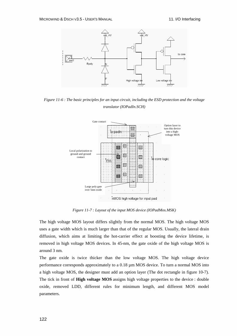
MICROWIND & DSCH V3.5 - USER'S MANUAL 11. I/O Interfacing
122
Figure 11-6 : The basic principles for an input circuit, including the ESD protection and the voltage
translator (IOPadIn.SCH)
Option layer to turn this device
into a high-voltage MOS
Local polarization to ground and ground
contact
Gate contact
Large poly gate over 5nm oxide
Figure 11-7 : Layout of the input MOS device (IOPadMos.MSK)
The high voltage MOS layout differs slightly from the normal MOS. The high voltage MOS
uses a gate width which is much larger than that of the regular MOS. Usually, the lateral drain
diffusion, which aims at limiting the hot-carrier effect at boosting the device lifetime, is
removed in high voltage MOS devices. In 45-nm, the gate oxide of the high voltage MOS is
around 3 nm.
The gate oxide is twice thicker than the low voltage MOS. The high voltage device
performance corresponds approximately to a 0.18 µm MOS device. To turn a normal MOS into
a high voltage MOS, the designer must add an option layer (The dot rectangle in figure 10-7).
The tick in front of High voltage MOS assigns high voltage properties to the device : double
oxide, removed LDD, different rules for minimum length, and different MOS model
parameters.
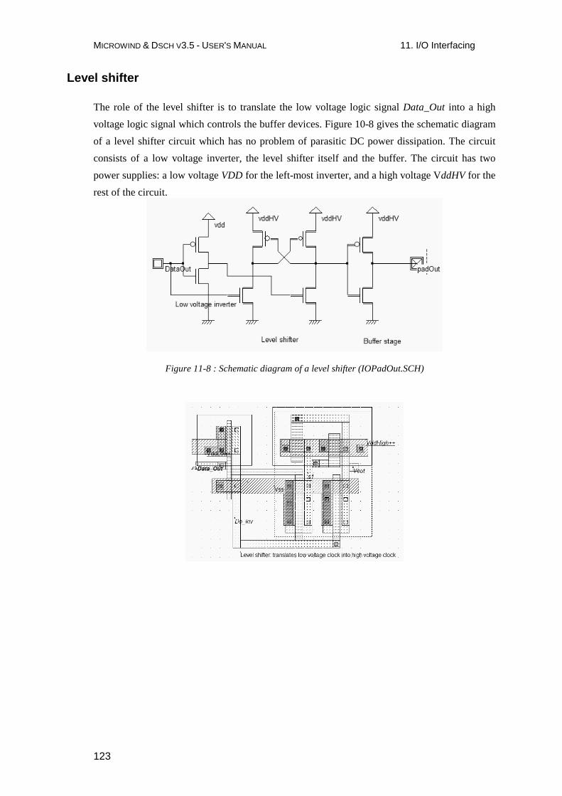
MICROWIND & DSCH V3.5 - USER'S MANUAL 11. I/O Interfacing
123
Level shifter
The role of the level shifter is to translate the low voltage logic signal Data_Out into a high
voltage logic signal which controls the buffer devices. Figure 10-8 gives the schematic diagram
of a level shifter circuit which has no problem of parasitic DC power dissipation. The circuit
consists of a low voltage inverter, the level shifter itself and the buffer. The circuit has two
power supplies: a low voltage VDD for the left-most inverter, and a high voltage VddHV for the
rest of the circuit.
Figure 11-8 : Schematic diagram of a level shifter (IOPadOut.SCH)

MICROWIND & DSCH V3.5 - USER'S MANUAL 11. I/O Interfacing
124
Figure 11-9 : Layout and simulation of the level shifter (LevelShift.MSK)
The layout of the level shifter is shown in figure 10-10. The left part works at low voltage 1.0
V, the right part works with high-voltage MOS devices, at a supply of 2.5V (VddHigh). The
data signal Data_Out has a 0-1.0 V voltage swing.
The output Vout has a 0-2.5V voltage swing. This time, no DC consumption appears except
during transitions of the logic signals, as shown in the simulation of figure 10-9.
Added Features in the Full version
Pad/Core limitation When the active area of the chip is the main limiting factor, the pad structure
may be designed in such a way that the width is large but the height is as small as possible. This situation, called "Core Limited", as well as its opposite "Pad limited" are detailed.
Schmitt trigger Using a Schmitt trigger instead of an inverter helps to transform a very noisy input signal into a clean logic signal. The Schmitt trigger circuit switching is illustrated and compared to the normal inverter.
Ibis IBIS is a standard for electronic behavioral specifications of integrated circuit input/output analog characteristics. MICROWIND uses IBIS to pilot the generation of pads.
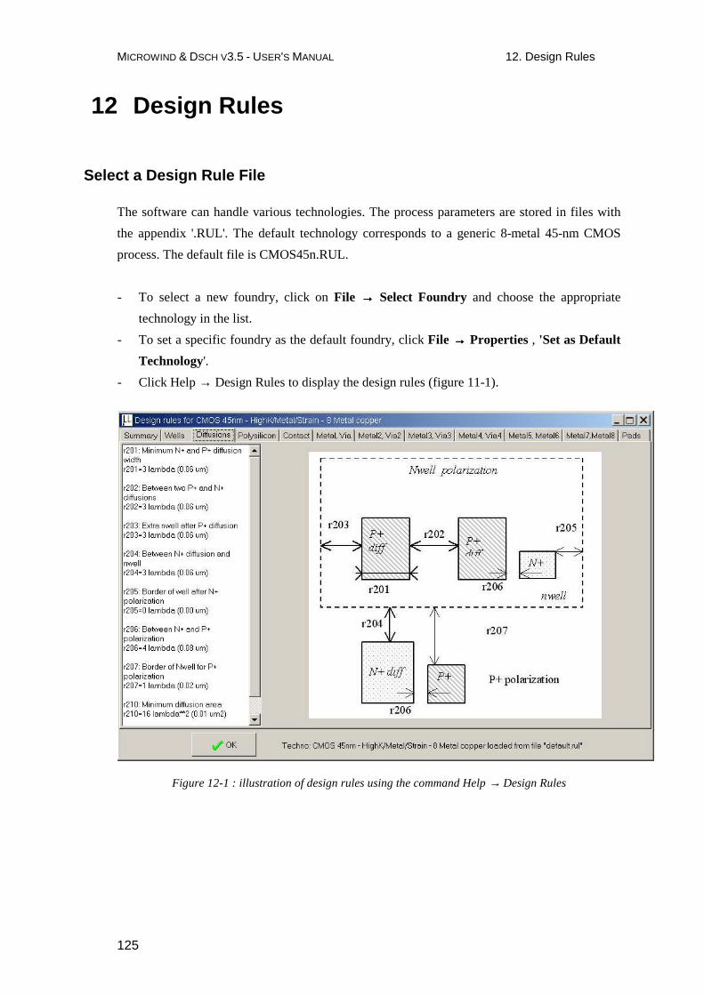
MICROWIND & DSCH V3.5 - USER'S MANUAL 12. Design Rules
125
Select a Design Rule File
The software can handle various technologies. The process parameters are stored in files with
the appendix '.RUL'. The default technology corresponds to a generic 8-metal 45-nm CMOS
process. The default file is CMOS45n.RUL.
- To select a new foundry, click on File →→→→ Select Foundry and choose the appropriate
technology in the list.
- To set a specific foundry as the default foundry, click File →→→→ Properties , 'Set as Default
Technology'.
- Click Help → Design Rules to display the design rules (figure 11-1).
Figure 12-1 : illustration of design rules using the command Help → Design Rules
12 Design Rules

MICROWIND & DSCH V3.5 - USER'S MANUAL 12. Design Rules
126
Lambda Units
The MICROWIND software works is based on a lambda grid, not on a micro grid. Consequently,
the same layout may be simulated in any CMOS technology. The value of lambda is half the
minimum polysilicon gate length. Table 11-1 gives the correspondence between lambda and
micron for all CMOS technologies available in version 3.5.
Technology file available in version 3.5
Minimum gate length
Value of lambda
Cmos12.rul 1.2 µm 0.60 µm Cmos08.rul 0.7 µm 0.35 µm Cmos06.rul 0.5 µm 0.25 µm Cmos035.rul 0.4 µm 0.20 µm Cmos025.rul 0.25 µm 0.125 µm Cmos018.rul 0.20 µm 0.100 µm Cmos012.rul 0.12 µm 0.060 µm soi012.rul (SOI version) 0.12 µm 0.060 µm Cmos90n.rul 0.10 µm 0.050 µm Cmos65n.rul 0.07 µm 0.035 µm Cmos45n.rul 0.05 µm 0.025 µm Cmos32n.rul 0.036 µm 0.018 µm
Table 11-1: correspondence between technology and the value of lambda in µm
N-Well
r101 r102 r110
Minimum well size Between wells Minimum well area
12 λ 12 λ 144 λ2 R101
R101
nwell
Diffusion
r201 r202 r203 r204: r205 r206 r207 r210
Minimum N+ and P+ diffusion width Between two P+ and N+ diffusions Extra nwell after P+ diffusion : Between N+ diffusion and nwell Border of well after N+ polarization Between N+ and P+ polarization Border of Nwell for P+ polarization Minimum diffusion area
4 λ 4 λ 6 λ 6 λ 2 λ 0 λ 6 λ 24 λ2 nwell
P+ diff P+ diff
N+ diff
r204
r202r203
r201
P+ P+ polarization
r207
N+
r205
Nwellpolarization
r206
r206
Polysilicon/Metal Gate

MICROWIND & DSCH V3.5 - USER'S MANUAL 12. Design Rules
127
Starting 45-nm, the polysilicon gate material has been replaced by metal such as NiSi. We keep
the name “polysilicon” for convenience.
r301 Polysilicon width 2λ
r302 Polysilicon gate on diffusion
2 λ
r303 Polysilicon gate on diffusion for high voltage MOS
4 λ
r304 Between two polysilicon boxes
3 λ
r305 Polysilicon vs. other diffusion
2 λ
r306 Diffusion after polysilicon
4 λ
r307 Extra gate after polysilicon
3 λ
r310 Minimum surface 8 λ2
P+diff
r305
r302r306
N+diff
r304r301
r306
r307
r303
High voltage MOS
2nd Polysilicon/Metal gate Design Rules
r311 Polysilicon2 width 2 λ
r312 Polysilicon2 gate on diffusion
2 λ
r320 Polysilicon2 minimum surface
8 λ2
Poly2r311
r312
MOS option
rOpt
Border of “option” layer over diff N+ and diff P+
7λ
N+difrOp

MICROWIND & DSCH V3.5 - USER'S MANUAL 12. Design Rules
128
Contact
r401 Contact width 2 λ
r402 Between two contacts 5 λ
r403
Extra diffusion over contact 2 λ
r404 Extra poly over contact 2 λ
r405 Extra metal over contact 2 λ
r406 Distance between contact and poly gate
3 λ
r407 Extra poly2 over contact 2 λ
r401
r402
contact polysilicium
r404
contact
gate
diffusion
r403
r406
metal
r405
Metal 1
r501 Metal width 4 λ
r502 Between two metals 4 λ
r510 Minimum surface 16 λ2
metal
r501
metalr502
Via
r601 Via width 2 λ
r602 Between two Via 5 λ
r603 Between Via and contact
0 λ
r604 Extra metal over via 2 λ
r605 Extra metal2 over via: 2 λ
r601
r602
viametal2
r604
contact
r603
Stacked via overcontactwhen r603 is 0
Metal 2
r701 Metal width:: 4 λ
r702 Between two metal2 4 λ
r710 Minimum surface 16 λ2 metal2
r701
metal2r702

MICROWIND & DSCH V3.5 - USER'S MANUAL 12. Design Rules
129
Via 2
r801 r802 r804 r805
Via2 width : 2 λ Between two Via2: 5 λ Extra metal2 over via2: 2 λ Extra metal3 over via2: 2 λ r801
r802
via2Metal3
r804
Metal 3
r901 r902 r910
Metal3 width: 4 λ Between two metal3 : 4 λ Minimum surface : 32 λ2 metal3
r901
metal3r902
Via 3
ra01 ra02 ra04 ra05
Via3 width : 2 λ Between two Via3: 5 λ Extra metal3 over via3: 2 λ Extra metal4 over via3: 2 λ
ra01
ra02
via3Metal3,4
ra04
Metal 4
rb01 rb02 rb10
Metal4 width: 4 λ Between two metal4 : 4 λ Minimum surface : 32 λ2 Metal4
rb01
Metal4rb02
Via 4
rc01 rc02 rc04 rc05
Via4 width : 2 λ Between two Via4: 5 λ Extra metal4 over via2: 3 λ Extra metal5 over via2: 3 λ
rc01
rc02
Via4
Metal4,5
rc04

MICROWIND & DSCH V3.5 - USER'S MANUAL 12. Design Rules
130
Metal 5
rd01 rd02 rd10
Metal5 width: 8 λ Between two metal5 : 8 λ Minimum surface : 100 λ2 Metal5
rd01
Metal5rd02
Via 5
re01 re02 re04 re05
Via5 width : 4 λ Between two Via5: 6 λ Extra metal5 over via5: 3 λ Extra metal6 over via5: 3 λ
re01
re02
Via5Metal5,6
re04
Metal 6
rf01 rf02 rf10
Metal6 width: 8 λ Between two metal6 : 15 λ Minimum surface : 300 λ2 Metal6
rf01
Metal6rf02
Via 6
rg01 rg02 rg04 rg05
Via6 width : 4 λ Between two Via6: 6 λ Extra metal6 over via6: 3 λ Extra metal7 over via6: 3 λ
rg01
rg02
Via6 Metal6,7
rg04
Metal 7
rh01 rh02 rh10
Metal7 width: 8 λ Between two metal7 : 15 λ Minimum surface : 300 λ2
Metal7
rh01
Metal7
rh02
Via 7
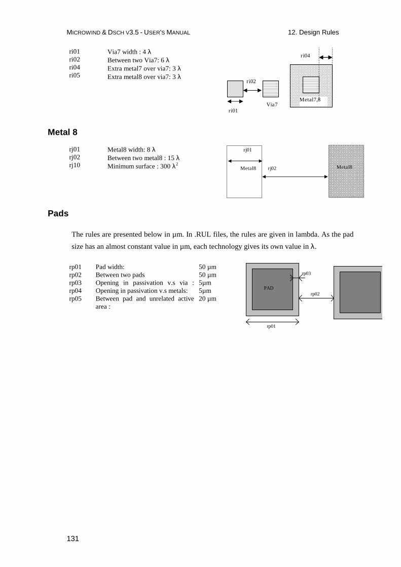
MICROWIND & DSCH V3.5 - USER'S MANUAL 12. Design Rules
131
ri01 ri02 ri04 ri05
Via7 width : 4 λ Between two Via7: 6 λ Extra metal7 over via7: 3 λ Extra metal8 over via7: 3 λ
ri01
ri02
Via7 Metal7,8
ri04
Metal 8
rj01 rj02 rj10
Metal8 width: 8 λ Between two metal8 : 15 λ Minimum surface : 300 λ2
Metal8
rj01
Metal8 rj02
Pads
The rules are presented below in µm. In .RUL files, the rules are given in lambda. As the pad
size has an almost constant value in µm, each technology gives its own value in λ.
rp01 rp02 rp03 rp04 rp05
Pad width: Between two pads Opening in passivation v.s via : Opening in passivation v.s metals: Between pad and unrelated active area :
50 µm 50 µm 5µm 5µm 20 µm
PAD
rp03
rp01
rp02
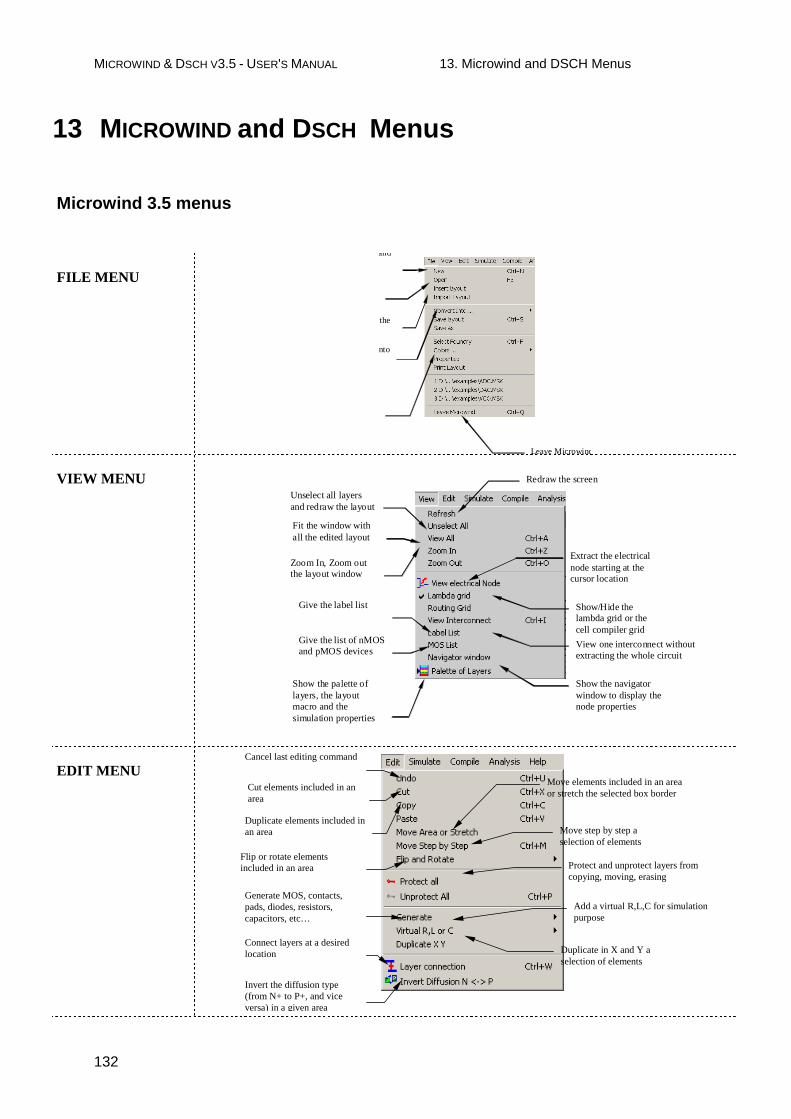
MICROWIND & DSCH V3.5 - USER'S MANUAL 13. Microwind and DSCH Menus
132
Microwind 3.5 menus
FILE MENU
Reset the program and
Insert a layout in the
Translates the layout into
Leave Microwind and
VIEW MENU
Unselect all layers and redraw the layout
Fit the window with all the edited layout
Zoom In, Zoom out the layout window
Give the list of nMOS and pMOS devices
Show/Hide the lambda grid or the cell compiler grid
Redraw the screen
Extract the electrical node starting at the cursor location
Show the navigator window to display the node properties
Show the palette of layers, the layout macro and the simulation properties
Give the label list
View one interconnect without extracting the whole circuit
EDIT MENU
Cancel last editing command
Cut elements included in an area
Duplicate elements included in an area
Generate MOS, contacts, pads, diodes, resistors, capacitors, etc…
Protect and unprotect layers from copying, moving, erasing
Move step by step a selection of elements
Move elements included in an area or stretch the selected box border
Flip or rotate elements included in an area
Duplicate in X and Y a selection of elements
Add a virtual R,L,C for simulation purpose
Connect layers at a desired location
Invert the diffusion type (from N+ to P+, and vice versa) in a given area
13 MICROWIND and DSCH Menus

MICROWIND & DSCH V3.5 - USER'S MANUAL 13. Microwind and DSCH Menus
133
SIMULATE MENU
Run the simulation and choose the appropriate mode V(t), I(t), V/V, F(t), etc…
Simulate directly on the layout, with a palette of colors representing voltage
Include crosstalk effects in simulation
Select model 1, model 3 or BSIM4
Access to the SPICE model sand some simulation options : VDD value, temperature, simulation step
2D view of the circuit at the desired location View the process steps of the
layout fabrication in static 3D
Access to static characteristics of the MOS devices
Discharge floating gates
Real-time view of the IC in full animated 3D
COMPILE MENU
Compile one single line (on-line)
Compile a Verilog file generated by DSCH2
ANALYSIS MENU
Verifies the layout and highlight the design rule violations
Computes the influence of one parameter such as VDD, t°, capacitance, on a set of parameters: delay, frequency, etc...
Evaluate the RC delay in all conductors using analytical formulations
Evaluate the crosstalk effect in all conductors using analytical formulations
Compute the resonant frequency of LC components
Measure the distance in the layout window, in µm and lambda
Compute the capacitance, resistance and inductance of one or two conductors above ground planes
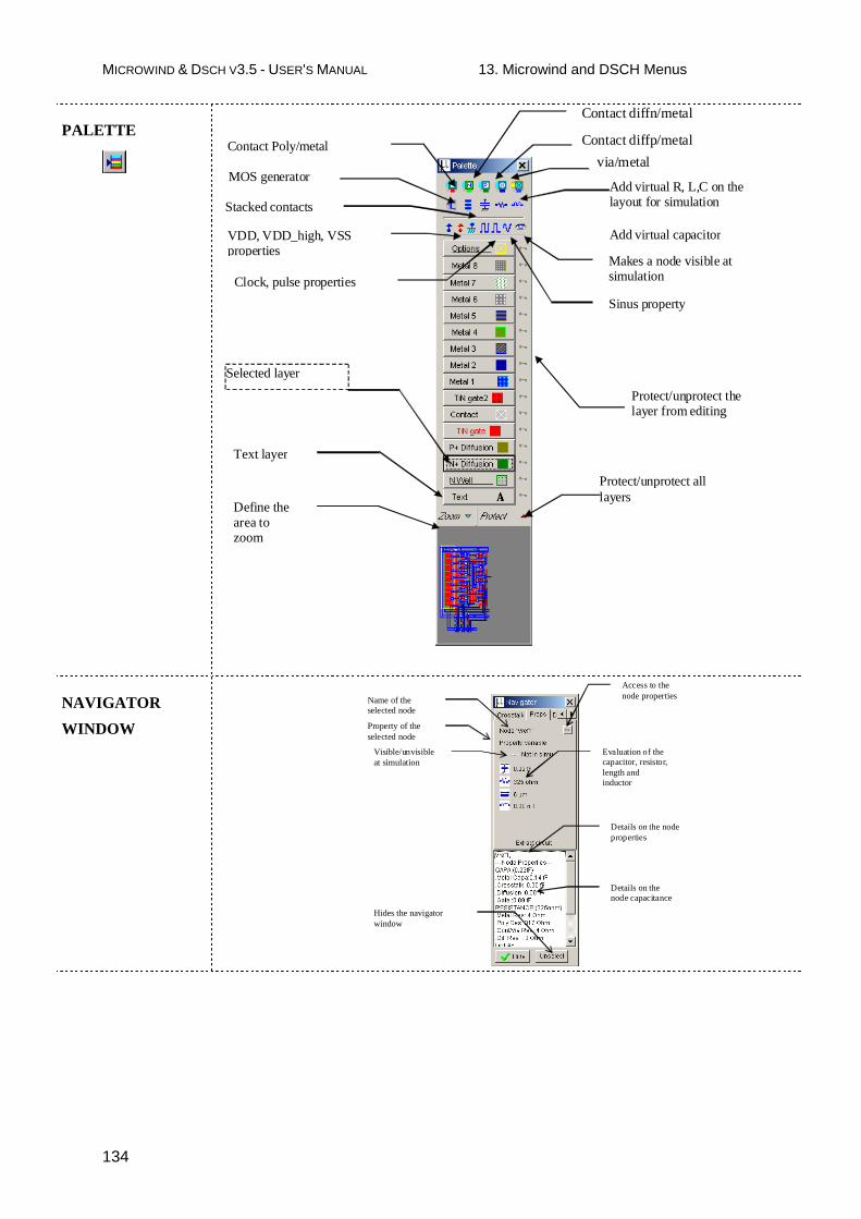
MICROWIND & DSCH V3.5 - USER'S MANUAL 13. Microwind and DSCH Menus
134
PALETTE
Contact diffn/metal
Contact diffp/metal
Stacked contacts
MOS generator
Add virtual capacitor
via/metal
Add virtual R, L,C on the layout for simulation
Selected layer
Protect/unprotect the layer from editing
Contact Poly/metal
VDD, VDD_high, VSS properties
Clock, pulse properties
Sinus property
Makes a node visible at simulation
Text layer
Protect/unprotect all layers
Define the area to zoom
NAVIGATOR
WINDOW
Name of the selected node
Property of the selected node
Visible/unvisible at simulation
Access to the node properties
Evaluation of the capacitor, resistor, length and inductor
Details on the node properties
Details on the node capacitance
Hides the navigator window

MICROWIND & DSCH V3.5 - USER'S MANUAL 13. Microwind and DSCH Menus
135
Select the node from which the delay counter is started at each crossing of VDD/2
The delay counter is stopped at each crossing of VDD/2 and the delay is drawn
Select the time scale within a list in the menu. Shift the time.
The minimum and maximum voltage of the selected node are displayed.
At each period of the selected node, the frequency is displayed
Computational simulation step
Restart simulation from time 0
More simulation
Stop simulation.
Node selected for calculations (FFT, min, max, freq..)
Show the FFT of the selected signal
Voltage versus time. Each visible node is displayed
Voltage and Currents versus time. All voltage on the bottom, all currents on the top.
Voltage versus voltage. Only a DC simulation, ideal for inverter, OpAmp static characteristics
Frequency vs. time. All voltage on the bottom, the switching frequency of the selected node on the top.
Eye diagram. A zoom at each visible node at the switching of a selected node
Evaluation of the power consumption
Access to MIN,TYP, MAX and MonteCarlo simulation
LIST OF ICONS
Open a layout file (MSK format)
Extract and simulate the circuit
Save the layout file in MSK format
Measure the distance in lambda and micron between two points
Draw a box using the selected layer of the palette
2D vertical aspect of the device
Delete boxes or text.
Animated 3D view of the layout using OpenGL
Copy boxes or text
Step by step fabrication of the layout in 3D
Stretch or move elements
Design rule checking of the circuit. Errors are notified in the layout
Zoom In
Add a text to the layout. The text may include simulation properties.
Zoom Out
Connect the lower to the upper layers at the desired
location using appropriate contacts.
View all the drawing
Static MOS characteristics
Extract and view the electrical node pointed by the cursor
View the palette
Move the layout up, left, right, down
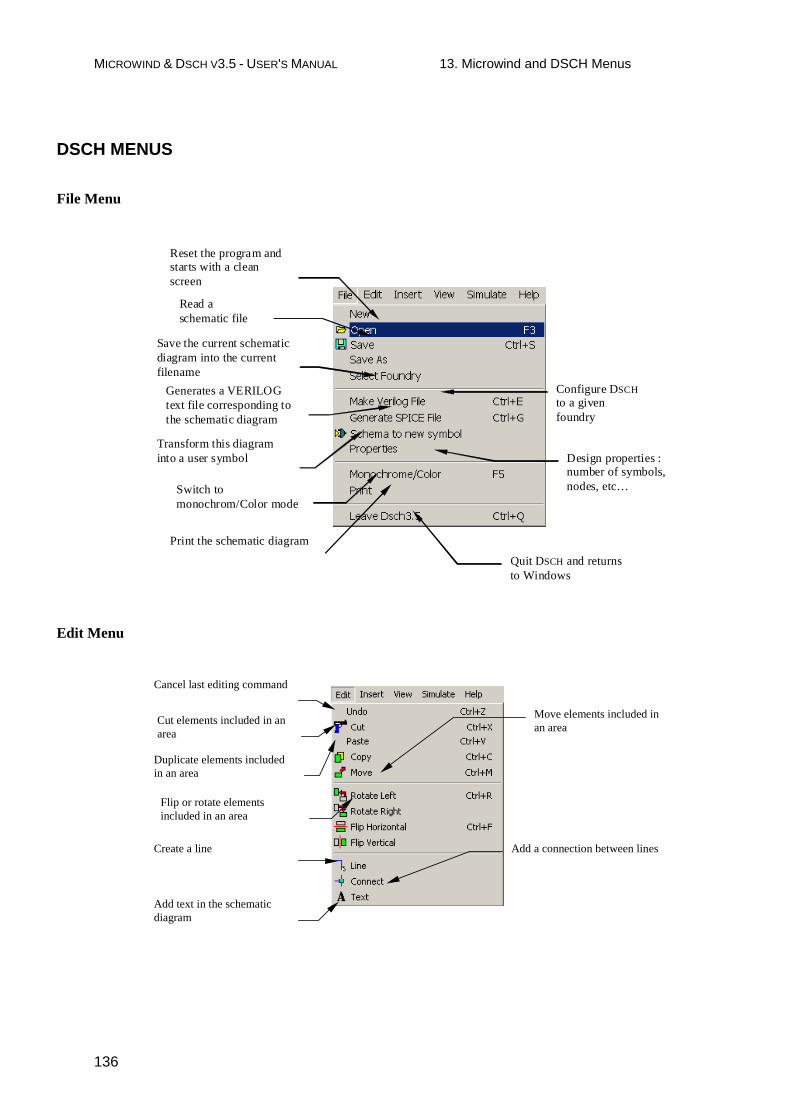
MICROWIND & DSCH V3.5 - USER'S MANUAL 13. Microwind and DSCH Menus
136
DSCH MENUS
File Menu
Reset the program and starts with a clean screen
Read a schematic file
Save the current schematic diagram into the current filename
Configure DSCH to a given foundry
Switch to monochrom/Color mode
Design properties : number of symbols, nodes, etc…
Print the schematic diagram
Quit DSCH and returns to Windows
Transform this diagram into a user symbol
Generates a VERILOG text file corresponding to the schematic diagram
Edit Menu
Cancel last editing command
Cut elements included in an area
Duplicate elements included in an area
Create a line
Move elements included in an area
Flip or rotate elements included in an area
Add a connection between lines
Add text in the schematic diagram
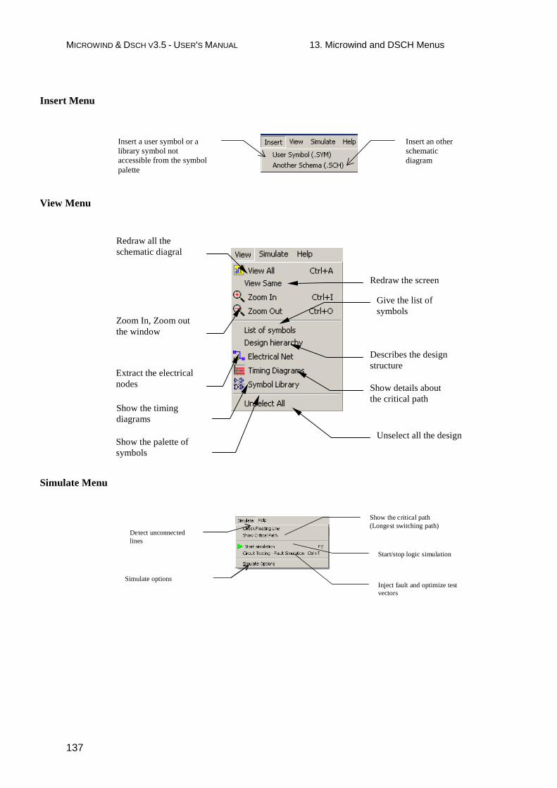
MICROWIND & DSCH V3.5 - USER'S MANUAL 13. Microwind and DSCH Menus
137
Insert Menu
Insert a user symbol or a library symbol not accessible from the symbol palette
Insert an other schematic diagram
View Menu
Redraw all the schematic diagral
Zoom In, Zoom out the window
Extract the electrical nodes
Describes the design structure
Redraw the screen
Give the list of symbols
Show details about the critical path
Show the timing diagrams
Show the palette of symbols
Unselect all the design
Simulate Menu
Detect unconnected lines
Show the critical path (Longest switching path)
Start/stop logic simulation
Simulate options Inject fault and optimize test vectors

MICROWIND & DSCH V3.5 - USER'S MANUAL 13. Microwind and DSCH Menus
138
Symbol Palette
Basic logic symbol library
Advanced logic symbol library
Button
VSS, VDD supply
Clock, led
Hexadecimal display
Inv, Inv 3state, buffer
AND gates
Hexadecimal keyboard
NAND gates
NOR gates
XOR gates
NMOS and PMOS
Complex gates
Memory
Latch
Edge-trigged D-latch
OR gates
Access to the complete symbol list
Basic logic symbol library
Advanced logic symbol library
Resistance (short circuit in logic simulation)
Capacitance (open circuit in logic simulation)
OpAm
Inductance (short circuit in logic simulation)
AND gates
Diode (ignored in logic simulation)
Random pattern generator (0, 1, x)
Complex display
XOR gates
Programmable switch
Dot box
Transmission gate
Multiplexor
Voltage source
Transmission line
Information probe
Current source
Electrical arrow
IO pads
Direct access to µC models

MICROWIND & DSCH V3.5 - USER'S MANUAL 13. Microwind and DSCH Menus
139
Silicon Menu
The software “silicon” is able to give a user’s controlled 3D view of silicon atoms such as SiO2 (figure 13-
1). The 3D view of the lattice shown in figure 12-3 shows the regular aspect of Si atoms and the very
specific properties of the material. One boron atom acts as a dopant in the structure.
Figure 13-1 : the « silicon » main menu

MICROWIND & DSCH V3.5 - USER'S MANUAL 13. Microwind and DSCH Menus
140
Figure 13-2 : the silicon lattice and a boron dopant
Researchers are actively exploring the use of molecular materials such as carbon nanotubes (CNTs)
in prototype molecular electronics devices. Atoms are bonded together into an array of hexagons
and rolled up to form molecular tubes or cylinders with 1 to 20 nm diameters and ranging from 100
nm to several microns in length. The CNT shown in Fig. 13-3 is formed of 12 carbon atoms.
Figure 13-3 : Carbon nano-tube

MICROWIND & DSCH V3.5 - USER'S MANUAL 13. Microwind and DSCH Menus
141
The fullerene C60 is based on 60 carbon atoms as shown in fig. 13-4. This structure has a diameter of around
1-nm. It is one of key candidates for emerging nanotechnology, thanks to its absorbing properties,
outstanding mechanical resistance, energy storage capabilities as well as potential interaction with
biological tissues for therapy.
Figure 13-4: Fullerene C60
Note: the CNT and fullerene have been implemented by INSA students Ryan FLOCH and Mathieu
OTHACEHE in 2010, as part of their 2nd year project in electronic design.

MICROWIND & DSCH V3.5 - USER'S MANUAL 15. References
142
www.microwind.org/students
The goal of this practical training is to illustrate the design of CMOS circuits with the help of Microwind.
The list of projects is illustrated in Fig. 14-1. For each project a report in PDF format is on-line.
Figure 14-1: student projects on-line, covering various aspects of circuit design
14 Student Projects on-line

MICROWIND & DSCH V3.5 - USER'S MANUAL 15. References
143
[Backer1998] R.J Backer, H. W. Li, D. E. Boyce "CMOS design, layout and simulation", IEEE Press, 1998, www.ieee.org
[Chau2004] R. Chau « Gate Dielectric Scaling for High-Performance CMOS : From SiO2 to High-K », IEDM Technical Digest, 2004
[Common2007] The Common Platform technology model is focused on 90-nm, 65-nm and 45-nm technology http://www.commonplatform.com/home
[Fujitsu2005] Okuno M. and al. « 45-nm Node CMOS Integration with a Novel STI Structure and Full-NCS/Cu Interlayers for Low-Operation-Power (LOP) Applications », Fujitsu Laboratories Ltd, proceedings of IEDM 2005
[Ghani2003] T. Ghani et. al. “A 90nm high volume manufacturing logic technology featuring novel 45nm gate length strained silicon CMOS transistors”, Digest of International Electron Devices Meeting 2003, IEDM ’03.
[Hastings2001] A. Hastings "The Art of Analog Layout", Prentice-Hall, 2001, ISBN 0-13-087061-7
[Lee1993] K. Lee, M. Shur, T.A Fjeldly, T. Ytterdal "Semiconductor Device Modeling for VLSI", Prentice Hall, 1993, ISBN 0-13-805656-0
[Lee2005] Lee, B.H, “Challenges in implementing high-k dielectrics in the 45nm technology node.”, 2005 International Conference on Integrated Circuit Design and Technology, ICICDT, May 2005 pp. 73 – 76
[Liu2001] W. Liu "Mosfet Models for SPICE simulation including Bsim3v3 and BSIM4", Wiley & Sons, 2001, ISBN 0-471-39697-4
[Moore1965] Moore, G. E., 1965, Cramming more components onto integrated circuits, Electronics, Volume 38, N°8.
[Nec2007] M. Tada “Feasibility Study of 45-nm-Node Scaled-Down Cu Interconnects With Molecular-Pore-Stacking (MPS) SiOCH Films, IEEE Trans. On Electron Devices, Vol. 54, No. 4, April 2007
[Osishi2005] Oishi, A “High performance CMOSFET technology for 45nm generation and scalability of stress-induced mobility enhancement technique”, IEEE International Electron Devices Meeting, 2005. IEDM Technical Digest. 2005 pp. 229 - 232
[Razavi2001] B. Razavi "Design of Analog CMOS integrated circuits", McGraw Hill, ISBN 0-07-238032-2, 2001, www.mhhe.com
[Sicard2005] E. Sicard, S. Ben Dhia “Basic CMOS cell design”, Tata McGraw Hill, 2005, ISBN 0-07-059933-5
[Sicard2005b] E. Sicard “Introducing 90-nm technology in Microwind3”, application note, July 2005, www.microwind.org
[Sicard2006] E. Sicard, M. Aziz “Introducing 65 nm technology in Microwind3”, application note available on www.microwind.org, August 2006.
[Sicard2007] E. Sicard, M. Aziz “Introducing 45-nm technology in Microwind3”, application note available on www.microwind.org, Oct. 2007.
[Sicard2010] E. Sicard, M. Aziz “Introducing 32-nm technology in Microwind 3.5”, application note available on www.microwind.org, May 2010.
[Song2006] S.C. Song “Highly Manufacturable Advanced Gate-Stack Technology for Sub 45-nm Self Aligned Gate-First CMOSFETs”, IEEE Trans. On Electron Devices, Vol. 53, pp 979-989, May 2006.....
[Sharma1996] A.K. Sharma "Semiconductor Memories", IEEE Press, 1996, ISBN 0-7803-1000-4
[Tsmc2004] Yang F. L and al. “45nm node planar-SOI technology with 0.296µm2 6T-SRAM cell”, Digest of Technical Papers, Symposium on VLSI Technology, 15-17 June 2004 pp 8-9.
[Tsai2003] W. Tsai, ‘‘Performance Comparison of Sub 1 nm Sputtered TiN/HfO2 nMOS and pMOSFETs,’’ IEDM Tech. Digest, p. 311 (2003).
15 References

144
ISBN 13 digit : 978-2-87649-057-4
First print : October 2009
Achevé d’imprimer : October 2009
Legal deposit : Décembre 2009
Dépôt legal : Décember 2009
Published by INSA Toulouse
University of Toulouse
135 Av de Rangueil
31077 Toulouse France