Embed Size (px)
Citation preview

Igor Lima de Paula
Wireless CommunicationMillimeter-Wave Active Opto-Electric Transmit Antenna for 5G
Academic year 2017-2018Faculty of Engineering and ArchitectureChair: Prof. dr. ir. Bart DhoedtDepartment of Information Technology
Master of Science in Electrical EngineeringMaster's dissertation submitted in order to obtain the academic degree of
CaytanCounsellors: ing. Quinten Van den Brande, Dr. ir. Sam Lemey, Joris Lambrecht, Ir. Olivier
Supervisors: Prof. dr. ir. Hendrik Rogier, Prof. dr. ir. Guy Torfs


Preface
This thesis is not my achievement alone, but rather the result of the collaboration with mysupervisors and counsellors to whom I express my enormous gratitude.
The supportive guidance and the insights offered by Prof. dr. ir. Hendrik Rogier and Prof.dr. ir. Guy Torfs, who tracked my progress with bi-weekly meetings, managed to bring thebest out of me. Along with the counsellors ing. Quinten Van den Brand, Dr. ir. Sam Lemey,Joris Lambrecht and ir. Olivier Caytan, who were always present to aid me with practical andtheoretical matters, they created a very structured environment. Actually, this is probably thebest environment in the world for a thesis student to take part. Quinten and Joris deservespecial acknowledgments for all the time invested and invaluable help in the manufacturing andmeasurements of the prototypes. All the measurement results related to antennas and to theactive opto-electric circuitry performed in the frame of this thesis are owed resp. to the co-workwith Quinten and Joris.
I would like to thank and to show my admiration to Dries Bosman who carried out a comple-mentary research to mine and who reciprocally shared his achievements in a very collaborativeway, without unnecessary competition.
I greatly appreciated the moments shared with the other thesis students, including Lars deBrabander, Laura Van Messem, Stijn Cuyvers and Stijn Poelman who contributed to a cozyand productive atmosphere in the thesis room and with whom I exchanged diverse insights.
I recognize the importance of my partner Saskia Wanner for being my Flemish/European(university-) culture personal advisor and for carefully listening to my theoretical explanationsat the end of days when my head was cluttered with the subject of my research – even thoughelectrical engineering is not her thing.
Last but not least, I could only be part of Ghent University as a Master student thanks tothe unconditional support and funding offered by my parents Maria das Graças Lima de Paulaand Luiz Rogerio de Paula. [Por último, mas não menos importante, eu só pude fazer parteda Universidade de Gante, como um estudante de mestrado, graças ao apoio incondicional eo financiamento oferecido por meus pais Maria das Graças Lima de Paula e Luiz Rogério dePaula.]
Igor Lima de Paula, May 2018

Admission to Loan
The author gives permission to make this master’s dissertation available for consultation andto copy parts of this master’s dissertation for personal use. In the case of any other use, thelimitations of the copyright have to be respected, in particular with regard to the obligation tostate expressly the source when quoting results from this master’s dissertation.
Igor Lima de Paula, May 2018
Millimeter-Wave Active Opto-ElectricTransmit Antenna for 5G Wireless
Communicationby
Igor LIMA DE PAULA
Master’s Dissertation submitted to obtain the academic degree ofMaster of Science in Electrical Engineering
Academic year 2017–2018
Supervisors: Prof. dr. ir. Hendrik ROGIER, Prof. dr. ir. Guy TORFS,Counsellors: ing. Quinten VAN DEN BRANDE, dr. ir. Sam LEMEY, ir. Joris LAMBRECHT,
ir. Olivier CAYTAN
Faculty of Engineering and ArchitectureGhent University
Department of Information TechnologyChairman: Prof. dr. ir. Bart DHOEDT
Summary
The present work introduces a highly-efficient active optically-enabled transmit antenna elementfor 5G phased-antenna arrays. The transmitter receives a Radio-over-Fiber optical signal in theC-band (1550 nm); converts it to the electrical domain by means of an in-house high-responsivityphotodiode; then a matching network of negligible insertion loss conveys the electrical signal(system band [27.5-29.5] GHz) to the commercial low noise amplifier HMC1040. Finally, thesignal, amplified by at least 24 dB, is transmitted to the air interface by an aperture-coupledpatch antenna which is backed by an air-filled substrate-integrated waveguide cavity. In thesystem band, the matching network achieves an insertion loss smaller than 0.3 dB; the antennatotal efficiency is greater than 97.5 %; the beamwidth in the principal planes is about 75° andthe front-to-back ratio is below 9.3 dB. The measured -10-dB-impedance band of the antennaitself is [24.19-32.33]GHz (28.4 %). Furthermore, its miniaturization along with the inherentself-shielding added by the cavity makes it suited for 5G phased-antenna arrays.
Keywords
millimeter wave, optoelectronics, active antenna, air-filled substrate-integrated waveguide (AF-SIW), Radio-over-Fiber (RoF), 5G wireless communication, phased-antenna array (PAA).
1
Millimeter-Wave Active Opto-Electric TransmitAntenna for 5G Wireless Communication
Igor Lima de PaulaSupervisors: Prof. dr. ir. Hendrik Rogier and prof. dr. ir. Guy Torfs
Counsellors: ing. Quinten Van den Brande, dr. ir. Sam Lemey, ir. Joris Lambrecht and ir. Olivier Caytan
Abstract—The present work introduces a highly-efficient ac-tive optically-enabled transmit antenna element for 5G phased-antenna arrays. The transmitter receives a Radio-over-Fiberoptical signal in the C-band (1550 nm); converts it to theelectrical domain by means of an in-house high-responsivityphotodiode; then a matching network of negligible insertionloss conveys the electrical signal (system band [27.5-29.5] GHz)to the commercial low noise amplifier HMC1040. Finally, thesignal, amplified by at least 24 dB, is transmitted to the airinterface by an aperture-coupled patch antenna which is backedby an air-filled substrate-integrated waveguide cavity. In thesystem band, the matching network achieves an insertion losssmaller than 0.3 dB; the antenna total efficiency is greater than97.5 %; the beamwidth in the principal planes is about 75°and the front-to-back ratio is above 9.3 dB. The measured -10-dB-impedance band of the antenna itself is [24.19-32.33] GHz(28.4 %). Furthermore, its miniaturization along with the in-herent self-shielding added by the cavity makes it suited for5G phased-antenna arrays.
Index Terms—millimeter wave, optoelectronics, active an-tenna, air-filled substrate-integrated waveguide (AFSIW),Radio-over-Fiber (RoF), 5G wireless communication, phased-antenna array (PAA).
I. Introduction
AS the new decade approaches, the transition to 5Gwireless networks starts to become reality [1]. The
upcoming applications and the change from a human-centered network to a paradigm dominated by human-to-machine and machine-to-machine connections [2] imposeunprecedented technical requirements in the coverage,data rate, latency, capacity to accommodate more con-nected devices, higher data traffic and energy and costefficiency. A key to achieve those goals is the massivedeployment of small cells [2]–[4].
As the global spectrum available below 6 GHz becomescongested and insufficient to provide for the near future[5], it is generally accepted by the academia and theindustry that at least a segment of 5G networks willoperate at bands above 20 GHz where there is plenty ofpotential spectrum to be explored [3]–[6]. At such highfrequencies, the electrical domain signal is subjected toincreased path loss. At the same time, the down scaling ofthe components, allows for phased-antenna arrays (PAAs)with large amount of elements to be built relativelycompactly. Therefore, such a technology is often cogitatedto counteract the increased path loss [7]–[9].
One way operators have been coping with such evolvingdemands is by deploying small cells through optically
connected remote antenna units (RAUs). This techniqueallows the implementation of very simple and cost-effectivebase stations whose complexity is centralized in a centraloffice (CO) [2], [10]. The optical domain is also verypromising when it comes to the realization of beamformingnetworks for PAAs which are arguably superior to theirelectrical-domain counterparts [11].
A handful of passive RAUs have been proposed in theliterature [12], [13]. However, either due to fiber or photo-diode (PD) nonlinearity, all-passive systems can typicallyhandle only a limited power [12] and are not suitable formillimeter wave (mmWave) 5G communications. Over thepast years, techniques have been proposed that implementpower transmission over fiber, allowing for an amplifier tobe integrated with a RAU without the need for externalpower supply [14], [15].
As reported by [4], [5], at mmWave, it is imperativeto bring the antenna as close as possible to the RadioFrequency (RF) circuitry such that it is directly printedon the same substrate as the RF circuitry thus avoidingthe high losses at cables, metal tracks and planar/non-planar transitions.
Recently, the air-filled substrate-integrated waveguide(AFSIW) technique was introduced [16] with whichhighly-efficient air-filled cavity-backed antennas could bedesigned [17]. Even though the efficiency of the antennaproposed in [17] is indeed high, its feeding scheme is non-planar and not appropriate for mmWave applications. In-stead, at mmWave, feeding a cavity-backed-configurationantenna by aperture coupling as reported in [18] is easierto fabricate and results in higher impedance bandwidth,which is characteristic of such feeding scheme.
The present work introduces an active optically-enabledtransmit antenna, which combines aperture coupling feed-ing with air-filled cavity backed configuration. It coversthe [27.5-29.5] GHz band and is highly attractive forapplications in 5G PAAs. The active opto-electric circuitryis compactly integrated in the back of the antenna anda careful full-wave/circuit co-optimization is carried outas in [19] in order to obtain a highly-efficient and reliabledesign.
The system architecture along with the specifications itis expected to comply with are described in section II. Thedesign aspects and results of the building blocks antennaand PD-to-LNA interconnect are presented respectivelyin section III and section IV. The conclusion and future
2
LNAMN
PD
DC bias
DC
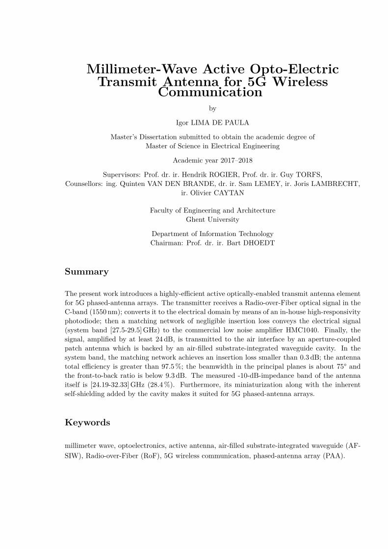
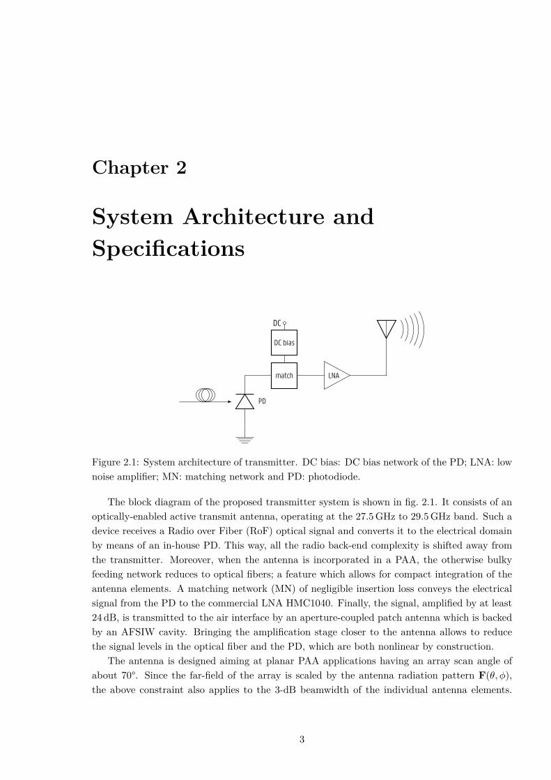
Fig. 1. System architecture of transmitter. DC bias: DC biasnetwork; LNA: low noise amplifier; MN: matching network and PD:photodiode.
research are exposed in section V.
II. System ArchitectureThe block diagram of the proposed transmitter system
is shown in fig. 1. It consists of an optically-enabled activetransmit antenna, operating at the band [27.5-29.5] GHz. Such a device receives a Radio over Fiber (RoF) opticalsignal and converts it to the electrical domain by means ofan in-house PD. This way, all the radio back-end complex-ity is shifted away from the transmitter. Moreover, whenthe antenna is incorporated in a PAA, the otherwise bulkyfeeding network reduces to optical fibers; a feature whichallows for compact integration of the antenna elements. Amatching network of negligible insertion loss conveys theelectrical signal from the PD to the commercial low noiseamplifier (LNA) HMC1040. Finally, the signal, amplifiedby at least 24 dB, is transmitted to the air interface byan aperture-coupled patch antenna which is backed byan AFSIW cavity. Bringing the amplification stage closerto the antenna allows to reduce the signal levels in theoptical fiber and the PD, which are both nonlinear byconstruction.
The antenna is designed aiming at planar PAA appli-cations having an array scan angle of about 70°. Since thefar-field of the array is scaled by the antenna radiation
yx
z
PCB3
PCB2
PCB1
1mm
0.254mm
0.254mm
Fig. 2. Exploded view of the AFCBPA featuring its 3 constituentPCBs. From top to bottom: PCB3, PCB2 and PCB1.
pattern F(θ, ϕ), the above constraint also applies to the3-dB beamwidth of the individual antenna elements. Anarray scan angle of 70° represents a compromise with themaximum gain of the antenna element. The importance ofthe latter in antenna arrays is evident when consideringthat a 3-dB increment in the elements’ maximum gainmeans that half the amount of antenna elements arenecessary to obtain the same antenna array gain. In orderfor the scan angle, 2|θ0max|, to be grating-lobe free, theinter-element spacing d is limited by [20],
d
λ0=
1
1 + sin |θ0max|(1)
which gives a maximum inter-element spacing comparedto the free-space wavelength of 0.64λ0 for 2|θ0max| = 70°.This imposes a harsh constraint on the the antennafunctional size taking into account that due to theirreduced ϵr, AFSIW components tend to be larger thantheir dielectric-filled SIW counterparts.
III. Air-Filled-Cavity-Backed Patch AntennaA. Antenna Specifications
The antenna is the building block that serves as anintegration platform for the transmitter. In this sense,its topology should be designed to conveniently andcompactly host the opto-active circuitry. A front-to-backratio FTBR ≥ 10 dB is aimed at so as to minimizethe susceptibility to such circuitry and to the eventualinstallation platform of the transmitter itself. It wasspecified in section II, that a 3-dB beamwidth ≈ 70°is required and the antenna must fit in a PAA withinter-element spacing of d = 6.45mm (considering λ0 atthe higher band edge f2 = 29.5GHz). A total efficiencyη ≥ 90% is imposed, which is realistic when it comes to
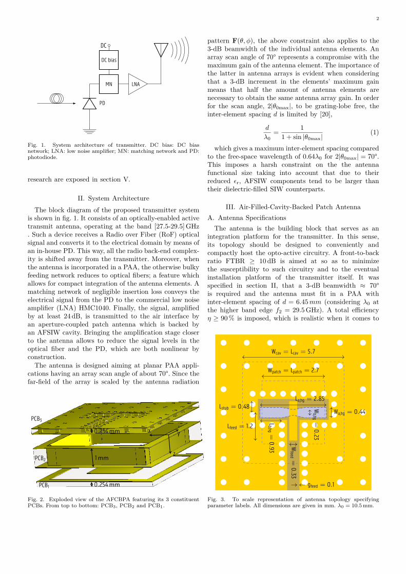
La,hg = 2.85
Wa,hg = 0.44
Wb,hg
=0.23
Lstub = 0.48
Lb,hg=0.93
Wpatch = Lpatch = 2.7
Wcav = Lcav = 5.7
Lfeed = 1.2
Wfeed
=0.33
gfeed = 0.1
Fig. 3. To scale representation of antenna topology specifyingparameter labels. All dimensions are given in mm. λ0 = 10.5mm.

3
20 22 24 26 28 30 32 34
−30
−20
−10
0
BW = 8.1GHz
frequency [GHz]
|S 11|[dB
]
meas.sim.
Fig. 4. Measured and simulated return loss of AFCBPA.
AFSIW antennas [17]. It is also implied that the antennashould be impedance matched over the system band withat least S11 < −10 dB.
B. Antenna Topology
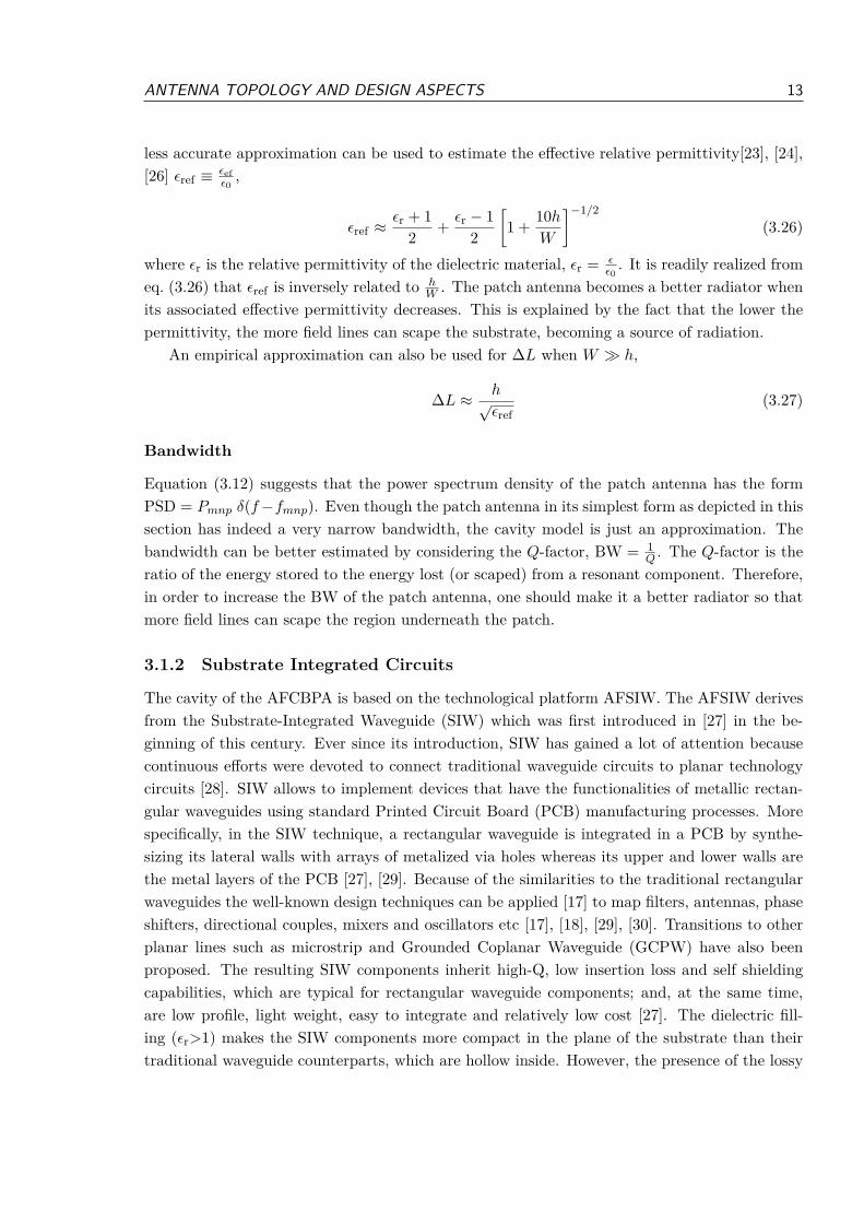
The exploded view of the AFCBPA is shown in fig. 2.It is an aperture coupled patch antenna whose patchlies over an air-filled cavity. Its feedline is realized inGrounded Coplanar Waveguide (GCPW) such that thereis a ground plane on the backside of the AFCBPA.This feeding scheme combines the enhanced impedancebandwidth and both broadside and cross-polarizationradiation purity offered by the aperture coupling withthe convenient platform for the RF circuity providedby the GCPW feedline. It is often desired to have suchcircuitry surrounded by a ground plane with interconnectsrealized as GCPW structures in order to prevent spuriousradiations. The GCPW ground is inherently compatiblewith it.
The air-filled cavity of the AFCBPA is based on theAFSIW technological platform [16], [17]. It consists of3 stacked PCBs, which are referred to as – from topto bottom of fig. 2 – PCB3, PCB2 and PCB1. A holecorresponding to the cavity size is milled away from PCB2
and the side walls are round-edge plated. The top andbottom walls of the cavity are represented by PCB3 andPCB1. The three PCBs are aligned and screwed together.Due to the air-filling, the dielectric losses are reduced to aminimum level, making the AFCBPA very energy efficient.The presence of the metalized cavity blocks surface wavesfrom propagating along the substrate. Avoiding surfacewaves is paramount for antenna array elements as theycan cause coupling with adjacent elements. A drawbackof AFSIW is that devices realized in this technique tendto be larger as a consequence of the reduced ϵr. However,the AFCBPA could be miniaturized due to the principleof mode splitting [17], [21] introduced by the couplingbetween the patch and the cavity. The dimensions of theantenna features are shown in fig. 3; note that indeed fora patch antenna in its simplest form, the length of thepatch is expected as λ0
2 whereas Lpatch ≈ λ0
4 .
030
60
90
120
150180
−150
−120
−90
−60
−30
−30
−20
−100
10 θ
directivity[dBi]
φ = 0meas.sim.
030
60
90
120
150180
−150
−120
−90
−60
−30
−30
−20
−100
10 θ
directivity[dBi]
φ = 90meas.sim.
Fig. 5. Measured and simulated H-plane and E-plane realized gaincuts of the AFCBPA at f0 = 28.5GHz.
The patch is etched on the metal layer of PCB1 as canbe seen in fig. 2; on the other of PCB1 there is no metallayer. The GCPW feedline is etched on the top metal layerof PCB3. The patch antenna ground plane is situatedon the other side of the PCB3substrate, containing anhourglass shaped aperture – best visualized from fig. 3– as part of the aperture coupling feeding arrangement.This ground plane and that of the GCPW are connectedthrough regularly spaced vias. Finally, to prevent that thetangential fields at the coupling aperture be attenuated,a rectangular slot is cut away from the GCPW groundsituated above the hourglass aperture.
Both substrates of PCB3 and PCB1 are fabricated in254 um RO4350B high frequency laminate (tan δ = 0.0037and ϵr = 3.66); whereas PCB2 is made of inexpensive1 mm FR-4 (tan δ = 0.024 and ϵr = 4.3). The antennaperformance is independent of the substrate of PCB2 asthe field strength in the remaining lossy FR-4 is ideallyzero. The manufacturer Eurocircuits is able to fabricateround-edge plated holes aside each other if a clearanceof 0.5 mm is respected. Due to the inherent self-shielding,minimal mutual coupling is expected even when cavitiesare very closely spaced. In this sense, keeping in mind thatthe cavity size is Wcav = 5.7mm, then the AFCBPA couldbe incorporated in a PAA with inter-element spacing of6.2 mm, which gives a margin of 250 um with respect tothe required value. This allows for a grating-lobe free scanangle of |2θ0max| = 80° at f2 = 29.5GHz.
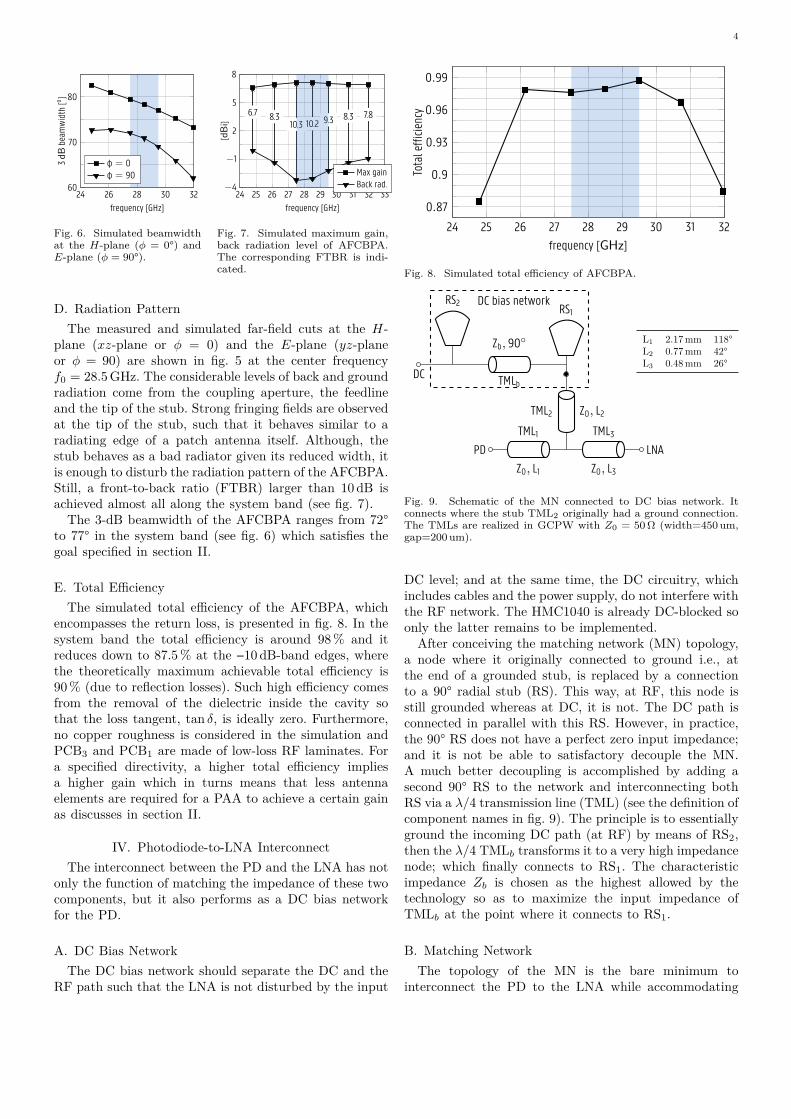
C. Return Loss
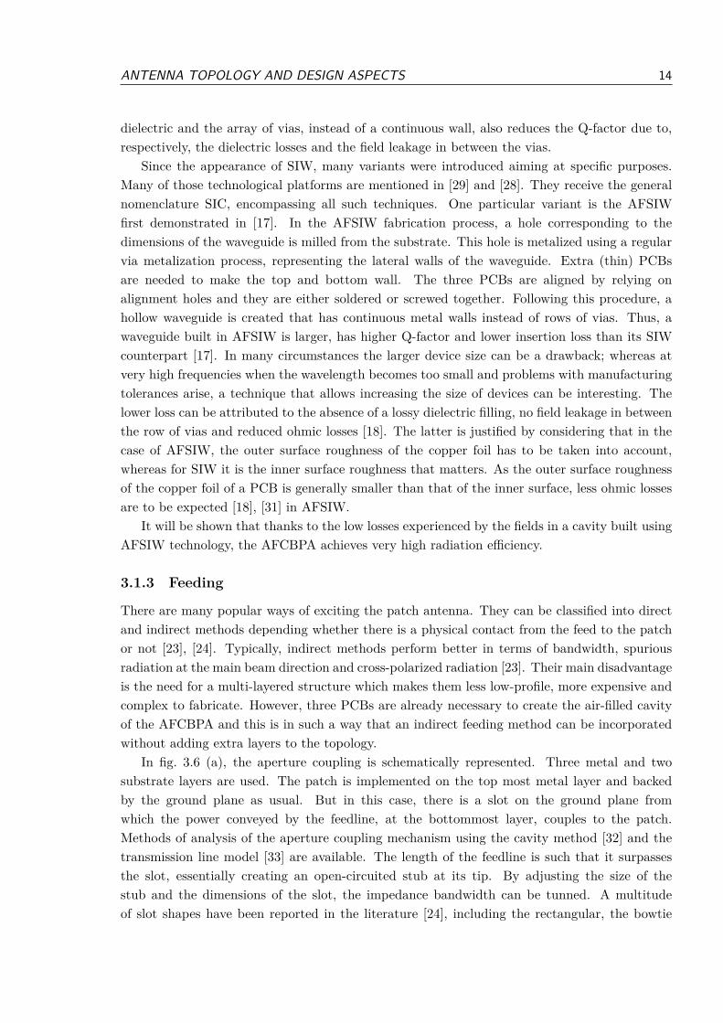
The AFCBPA achieves a -10-dB impedance bandwidthof [24.19-32.33] GHz (8.1 GHz or 28.4 %) as seen fromits return loss in fig. 4. This is owed to a resonanceloop occurring in its reflection coefficient in response tocoupling of the patch either with the cavity or with thefeeding aperture. By properly adjusting the dimensionsof the aperture in combination with the stub length, thesize of the loop can be enlarged and centered in the Smithchart. The hourglass shape of the coupling aperture waschosen so as to obtain more degrees of freedom whenadjusting it in the optimization phase. The increasedbandwidth can also be attributed to the low permittivityunderneath the patch, reducing the antenna Q-factor [17].
4
24 26 28 30 3260
70
80
frequency [GHz]
3dBbeamwidth[o]
φ = 0φ = 90
Fig. 6. Simulated beamwidthat the H-plane (ϕ = 0°) andE-plane (ϕ = 90°).
24 25 26 27 28 29 30 31 32 33−4
−1
2
5
8
6.7 8.310.3 10.2 9.3 8.3 7.8
frequency [GHz]
[dBi]
Max gainBack rad.
Fig. 7. Simulated maximum gain,back radiation level of AFCBPA.The corresponding FTBR is indi-cated.
D. Radiation PatternThe measured and simulated far-field cuts at the H-
plane (xz-plane or ϕ = 0) and the E-plane (yz-planeor ϕ = 90) are shown in fig. 5 at the center frequencyf0 = 28.5GHz. The considerable levels of back and groundradiation come from the coupling aperture, the feedlineand the tip of the stub. Strong fringing fields are observedat the tip of the stub, such that it behaves similar to aradiating edge of a patch antenna itself. Although, thestub behaves as a bad radiator given its reduced width, itis enough to disturb the radiation pattern of the AFCBPA.Still, a front-to-back ratio (FTBR) larger than 10 dB isachieved almost all along the system band (see fig. 7).
The 3-dB beamwidth of the AFCBPA ranges from 72°to 77° in the system band (see fig. 6) which satisfies thegoal specified in section II.
E. Total EfficiencyThe simulated total efficiency of the AFCBPA, which
encompasses the return loss, is presented in fig. 8. In thesystem band the total efficiency is around 98 % and itreduces down to 87.5 % at the −10 dB-band edges, wherethe theoretically maximum achievable total efficiency is90 % (due to reflection losses). Such high efficiency comesfrom the removal of the dielectric inside the cavity sothat the loss tangent, tan δ, is ideally zero. Furthermore,no copper roughness is considered in the simulation andPCB3 and PCB1 are made of low-loss RF laminates. Fora specified directivity, a higher total efficiency impliesa higher gain which in turns means that less antennaelements are required for a PAA to achieve a certain gainas discusses in section II.
IV. Photodiode-to-LNA InterconnectThe interconnect between the PD and the LNA has not
only the function of matching the impedance of these twocomponents, but it also performs as a DC bias networkfor the PD.
A. DC Bias NetworkThe DC bias network should separate the DC and the
RF path such that the LNA is not disturbed by the input
24 25 26 27 28 29 30 31 32
0.87
0.9
0.93
0.96
0.99
frequency [GHz]
Totalefficiency
Fig. 8. Simulated total efficiency of AFCBPA.
L1 2.17 mm 118°L2 0.77 mm 42°L3 0.48 mm 26°
PDTML1
Z0, L1
TML2 Z0, L2TML3
Z0, L3
LNA
RS1
TMLb
Zb, 90
RS2
DC
DC bias network
Fig. 9. Schematic of the MN connected to DC bias network. Itconnects where the stub TML2 originally had a ground connection.The TMLs are realized in GCPW with Z0 = 50Ω (width=450 um,gap=200 um).
DC level; and at the same time, the DC circuitry, whichincludes cables and the power supply, do not interfere withthe RF network. The HMC1040 is already DC-blocked soonly the latter remains to be implemented.
After conceiving the matching network (MN) topology,a node where it originally connected to ground i.e., atthe end of a grounded stub, is replaced by a connectionto a 90° radial stub (RS). This way, at RF, this node isstill grounded whereas at DC, it is not. The DC path isconnected in parallel with this RS. However, in practice,the 90° RS does not have a perfect zero input impedance;and it is not be able to satisfactory decouple the MN.A much better decoupling is accomplished by adding asecond 90° RS to the network and interconnecting bothRS via a λ/4 transmission line (TML) (see the definition ofcomponent names in fig. 9). The principle is to essentiallyground the incoming DC path (at RF) by means of RS2,then the λ/4 TMLb transforms it to a very high impedancenode; which finally connects to RS1. The characteristicimpedance Zb is chosen as the highest allowed by thetechnology so as to maximize the input impedance ofTMLb at the point where it connects to RS1.
B. Matching NetworkThe topology of the MN is the bare minimum to
interconnect the PD to the LNA while accommodating
5
26.5 27 27.5 28 28.5 29 29.5 30 30.5−30
−25
−20
−15
−10
frequency [GHz]
|S ii|[dB
]
|S22,MN2 ||S11,MN2 |
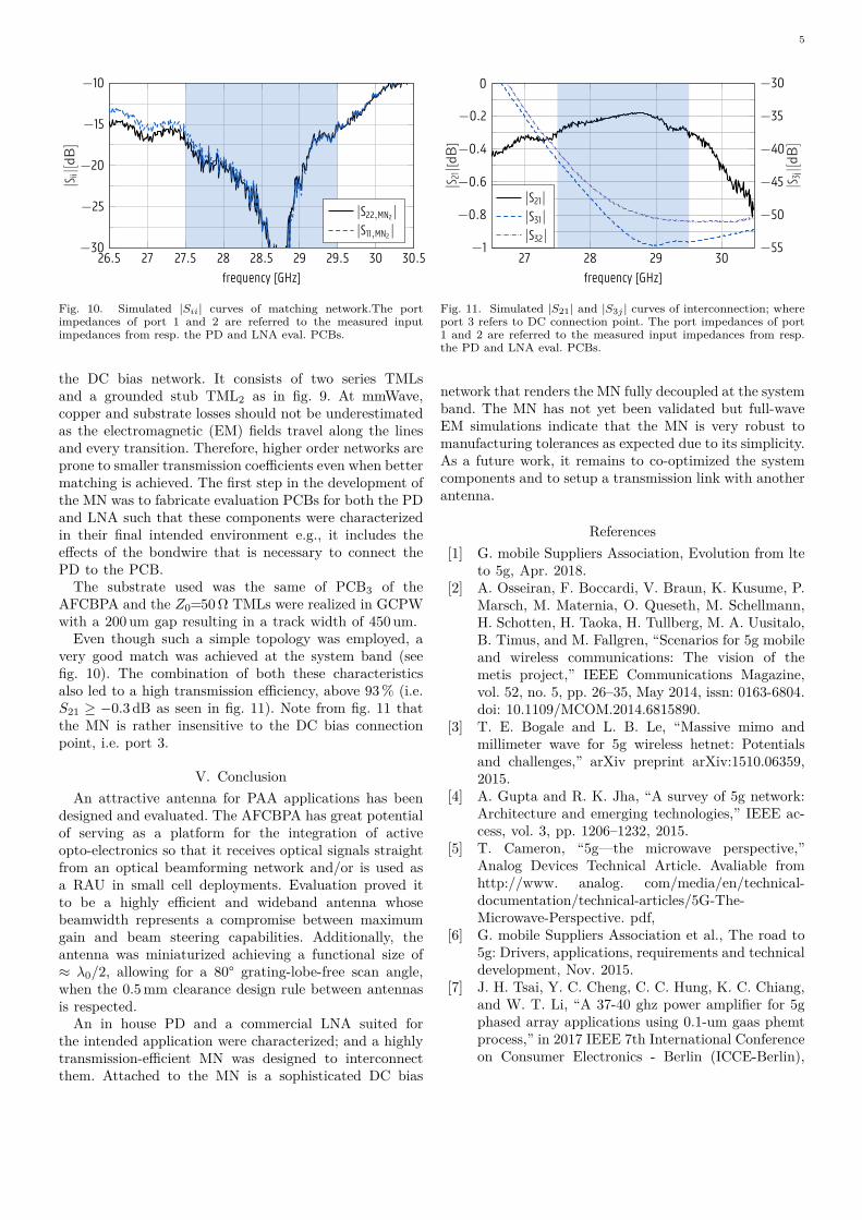
Fig. 10. Simulated |Sii| curves of matching network.The portimpedances of port 1 and 2 are referred to the measured inputimpedances from resp. the PD and LNA eval. PCBs.
the DC bias network. It consists of two series TMLsand a grounded stub TML2 as in fig. 9. At mmWave,copper and substrate losses should not be underestimatedas the electromagnetic (EM) fields travel along the linesand every transition. Therefore, higher order networks areprone to smaller transmission coefficients even when bettermatching is achieved. The first step in the development ofthe MN was to fabricate evaluation PCBs for both the PDand LNA such that these components were characterizedin their final intended environment e.g., it includes theeffects of the bondwire that is necessary to connect thePD to the PCB.
The substrate used was the same of PCB3 of theAFCBPA and the Z0=50Ω TMLs were realized in GCPWwith a 200 um gap resulting in a track width of 450 um.
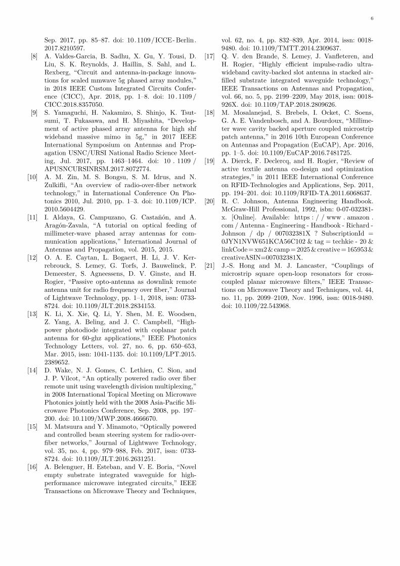
Even though such a simple topology was employed, avery good match was achieved at the system band (seefig. 10). The combination of both these characteristicsalso led to a high transmission efficiency, above 93 % (i.e.S21 ≥ −0.3 dB as seen in fig. 11). Note from fig. 11 thatthe MN is rather insensitive to the DC bias connectionpoint, i.e. port 3.
V. ConclusionAn attractive antenna for PAA applications has been
designed and evaluated. The AFCBPA has great potentialof serving as a platform for the integration of activeopto-electronics so that it receives optical signals straightfrom an optical beamforming network and/or is used asa RAU in small cell deployments. Evaluation proved itto be a highly efficient and wideband antenna whosebeamwidth represents a compromise between maximumgain and beam steering capabilities. Additionally, theantenna was miniaturized achieving a functional size of≈ λ0/2, allowing for a 80° grating-lobe-free scan angle,when the 0.5 mm clearance design rule between antennasis respected.
An in house PD and a commercial LNA suited forthe intended application were characterized; and a highlytransmission-efficient MN was designed to interconnectthem. Attached to the MN is a sophisticated DC bias
27 28 29 30−1
−0.8
−0.6
−0.4
−0.2
0
−55
−50
−45
−40
−35
−30
frequency [GHz]
|S 21|[dB]
|S 3j|[dB
]
|S21||S31||S32|
Fig. 11. Simulated |S21| and |S3j | curves of interconnection; whereport 3 refers to DC connection point. The port impedances of port1 and 2 are referred to the measured input impedances from resp.the PD and LNA eval. PCBs.
network that renders the MN fully decoupled at the systemband. The MN has not yet been validated but full-waveEM simulations indicate that the MN is very robust tomanufacturing tolerances as expected due to its simplicity.As a future work, it remains to co-optimized the systemcomponents and to setup a transmission link with anotherantenna.
References[1] G. mobile Suppliers Association, Evolution from lte
to 5g, Apr. 2018.[2] A. Osseiran, F. Boccardi, V. Braun, K. Kusume, P.
Marsch, M. Maternia, O. Queseth, M. Schellmann,H. Schotten, H. Taoka, H. Tullberg, M. A. Uusitalo,B. Timus, and M. Fallgren, “Scenarios for 5g mobileand wireless communications: The vision of themetis project,” IEEE Communications Magazine,vol. 52, no. 5, pp. 26–35, May 2014, issn: 0163-6804.doi: 10.1109/MCOM.2014.6815890.
[3] T. E. Bogale and L. B. Le, “Massive mimo andmillimeter wave for 5g wireless hetnet: Potentialsand challenges,” arXiv preprint arXiv:1510.06359,2015.
[4] A. Gupta and R. K. Jha, “A survey of 5g network:Architecture and emerging technologies,” IEEE ac-cess, vol. 3, pp. 1206–1232, 2015.
[5] T. Cameron, “5g—the microwave perspective,”Analog Devices Technical Article. Avaliable fromhttp://www. analog. com/media/en/technical-documentation/technical-articles/5G-The-Microwave-Perspective. pdf,
[6] G. mobile Suppliers Association et al., The road to5g: Drivers, applications, requirements and technicaldevelopment, Nov. 2015.
[7] J. H. Tsai, Y. C. Cheng, C. C. Hung, K. C. Chiang,and W. T. Li, “A 37-40 ghz power amplifier for 5gphased array applications using 0.1-um gaas phemtprocess,” in 2017 IEEE 7th International Conferenceon Consumer Electronics - Berlin (ICCE-Berlin),
6
Sep. 2017, pp. 85–87. doi: 10.1109/ICCE- Berlin.2017.8210597.
[8] A. Valdes-Garcia, B. Sadhu, X. Gu, Y. Tousi, D.Liu, S. K. Reynolds, J. Haillin, S. Sahl, and L.Rexberg, “Circuit and antenna-in-package innova-tions for scaled mmwave 5g phased array modules,”in 2018 IEEE Custom Integrated Circuits Confer-ence (CICC), Apr. 2018, pp. 1–8. doi: 10 . 1109 /CICC.2018.8357050.
[9] S. Yamaguchi, H. Nakamizo, S. Shinjo, K. Tsut-sumi, T. Fukasawa, and H. Miyashita, “Develop-ment of active phased array antenna for high shfwideband massive mimo in 5g,” in 2017 IEEEInternational Symposium on Antennas and Prop-agation USNC/URSI National Radio Science Meet-ing, Jul. 2017, pp. 1463–1464. doi: 10 . 1109 /APUSNCURSINRSM.2017.8072774.
[10] A. M. Zin, M. S. Bongsu, S. M. Idrus, and N.Zulkifli, “An overview of radio-over-fiber networktechnology,” in International Conference On Pho-tonics 2010, Jul. 2010, pp. 1–3. doi: 10.1109/ICP.2010.5604429.
[11] I. Aldaya, G. Campuzano, G. Castañón, and A.Aragón-Zavala, “A tutorial on optical feeding ofmillimeter-wave phased array antennas for com-munication applications,” International Journal ofAntennas and Propagation, vol. 2015, 2015.
[12] O. A. E. Caytan, L. Bogaert, H. Li, J. V. Ker-rebrouck, S. Lemey, G. Torfs, J. Bauwelinck, P.Demeester, S. Agneessens, D. V. Ginste, and H.Rogier, “Passive opto-antenna as downlink remoteantenna unit for radio frequency over fiber,” Journalof Lightwave Technology, pp. 1–1, 2018, issn: 0733-8724. doi: 10.1109/JLT.2018.2834153.
[13] K. Li, X. Xie, Q. Li, Y. Shen, M. E. Woodsen,Z. Yang, A. Beling, and J. C. Campbell, “High-power photodiode integrated with coplanar patchantenna for 60-ghz applications,” IEEE PhotonicsTechnology Letters, vol. 27, no. 6, pp. 650–653,Mar. 2015, issn: 1041-1135. doi: 10.1109/LPT.2015.2389652.
[14] D. Wake, N. J. Gomes, C. Lethien, C. Sion, andJ. P. Vilcot, “An optically powered radio over fiberremote unit using wavelength division multiplexing,”in 2008 International Topical Meeting on MicrowavePhotonics jointly held with the 2008 Asia-Pacific Mi-crowave Photonics Conference, Sep. 2008, pp. 197–200. doi: 10.1109/MWP.2008.4666670.
[15] M. Matsuura and Y. Minamoto, “Optically poweredand controlled beam steering system for radio-over-fiber networks,” Journal of Lightwave Technology,vol. 35, no. 4, pp. 979–988, Feb. 2017, issn: 0733-8724. doi: 10.1109/JLT.2016.2631251.
[16] A. Belenguer, H. Esteban, and V. E. Boria, “Novelempty substrate integrated waveguide for high-performance microwave integrated circuits,” IEEETransactions on Microwave Theory and Techniques,
vol. 62, no. 4, pp. 832–839, Apr. 2014, issn: 0018-9480. doi: 10.1109/TMTT.2014.2309637.
[17] Q. V. den Brande, S. Lemey, J. Vanfleteren, andH. Rogier, “Highly efficient impulse-radio ultra-wideband cavity-backed slot antenna in stacked air-filled substrate integrated waveguide technology,”IEEE Transactions on Antennas and Propagation,vol. 66, no. 5, pp. 2199–2209, May 2018, issn: 0018-926X. doi: 10.1109/TAP.2018.2809626.
[18] M. Mosalanejad, S. Brebels, I. Ocket, C. Soens,G. A. E. Vandenbosch, and A. Bourdoux, “Millime-ter wave cavity backed aperture coupled microstrippatch antenna,” in 2016 10th European Conferenceon Antennas and Propagation (EuCAP), Apr. 2016,pp. 1–5. doi: 10.1109/EuCAP.2016.7481725.
[19] A. Dierck, F. Declercq, and H. Rogier, “Review ofactive textile antenna co-design and optimizationstrategies,” in 2011 IEEE International Conferenceon RFID-Technologies and Applications, Sep. 2011,pp. 194–201. doi: 10.1109/RFID-TA.2011.6068637.
[20] R. C. Johnson, Antenna Engineering Handbook.McGraw-Hill Professional, 1992, isbn: 0-07-032381-x. [Online]. Available: https : / / www . amazon .com / Antenna - Engineering - Handbook - Richard -Johnson / dp / 007032381X ? SubscriptionId =0JYN1NVW651KCA56C102 & tag = techkie - 20 &linkCode=xm2&camp=2025&creative=165953&creativeASIN=007032381X.
[21] J.-S. Hong and M. J. Lancaster, “Couplings ofmicrostrip square open-loop resonators for cross-coupled planar microwave filters,” IEEE Transac-tions on Microwave Theory and Techniques, vol. 44,no. 11, pp. 2099–2109, Nov. 1996, issn: 0018-9480.doi: 10.1109/22.543968.

Contents
List of Figures xv
List of Tables xix
1 Introduction 11.1 Outline . . . . . . . . . . . . . . . . . . . . . . . . . . . . . . . . . . . . . . . . . 2
2 System Architecture and Specifications 3
3 Antenna Topology and Design Aspects 53.1 Basic Concepts . . . . . . . . . . . . . . . . . . . . . . . . . . . . . . . . . . . . . 5
3.1.1 Rectangular Patch Antenna . . . . . . . . . . . . . . . . . . . . . . . . . . 53.1.2 Substrate Integrated Circuits . . . . . . . . . . . . . . . . . . . . . . . . . 133.1.3 Feeding . . . . . . . . . . . . . . . . . . . . . . . . . . . . . . . . . . . . . 14
3.2 Air-Filled Cavity Backed Patch Antenna . . . . . . . . . . . . . . . . . . . . . . . 163.2.1 Parametric Analysis . . . . . . . . . . . . . . . . . . . . . . . . . . . . . . 23
3.3 Validation . . . . . . . . . . . . . . . . . . . . . . . . . . . . . . . . . . . . . . . . 33
4 Active Opto-Electronic Circuitry 364.1 Low Noise Amplifier . . . . . . . . . . . . . . . . . . . . . . . . . . . . . . . . . . 364.2 Photodiode . . . . . . . . . . . . . . . . . . . . . . . . . . . . . . . . . . . . . . . 394.3 Photodiode to LNA Interconnection . . . . . . . . . . . . . . . . . . . . . . . . . 42
4.3.1 DC Bias Network . . . . . . . . . . . . . . . . . . . . . . . . . . . . . . . . 424.3.2 Impedance Matching Network Version 1 . . . . . . . . . . . . . . . . . . . 444.3.3 Impedance Matching Network Version 2 . . . . . . . . . . . . . . . . . . . 55
5 Conclusion and Future Research 61
A Phase of S11 of an Ideal Transmission Line 67
B True, Reflect, Line Calibration 68
xiv

List of Figures
2.1 System architecture of transmitter. DC bias: DC bias network of the PD; LNA:low noise amplifier; MN: matching network and PD: photodiode. . . . . . . . . . 3
3.1 Patch antenna isometric view dimensions . . . . . . . . . . . . . . . . . . . . . . 63.2 Patch antenna fundamental TM10 mode profile. . . . . . . . . . . . . . . . . . . . 63.3 Patch antenna isometric view axis . . . . . . . . . . . . . . . . . . . . . . . . . . 73.4 Patch antenna cavity featuring electric field (E-field) . . . . . . . . . . . . . . . . 103.5 Patch antenna featuring principal planes . . . . . . . . . . . . . . . . . . . . . . . 113.6 Aperture coupling: schematic representation . . . . . . . . . . . . . . . . . . . . . 153.7 Aperture coupling slot shapes . . . . . . . . . . . . . . . . . . . . . . . . . . . . . 153.8 Exploded view of the proposed antenna . . . . . . . . . . . . . . . . . . . . . . . 173.9 Schematic representation of antenna topology specifying parameter labels. All
shapes are to scale. . . . . . . . . . . . . . . . . . . . . . . . . . . . . . . . . . . . 183.10 E-field components inside the antenna cavity . . . . . . . . . . . . . . . . . . . . 203.11 Return loss of the air-filled-cavity-backed patch antenna (AFCBPA). . . . . . . . 213.12 magnetic field plane (H-plane) and electric field plane (E-plane) directivity cuts
of the AFCBPA at f0 = 28.5GHz. . . . . . . . . . . . . . . . . . . . . . . . . . . 223.13 Beamwidth at the H-plane (ϕ = 0°) and E-plane (ϕ = 90°) directivity cuts of
the AFCBPA versus the frequency. . . . . . . . . . . . . . . . . . . . . . . . . . . 233.14 Max gain, back radiation level and front-to-back ratio (FTBR) of the AFCBPA
versus the frequency. . . . . . . . . . . . . . . . . . . . . . . . . . . . . . . . . . . 233.15 Total efficiency of the AFCBPA along the frequency f . . . . . . . . . . . . . . . . 233.16 Effect of varying the parameter Lstub on the return loss of the AFCBPA. . . . . . 263.17 Effect of varying the parameter Lstub on the directivity related figures of merit of
the AFCBPA. . . . . . . . . . . . . . . . . . . . . . . . . . . . . . . . . . . . . . . 263.18 Effect of varying the parameter La,hg on the return loss of the AFCBPA. . . . . . 273.19 Effect of varying the parameter La,hg on the directivity related figures of merit of
the AFCBPA. . . . . . . . . . . . . . . . . . . . . . . . . . . . . . . . . . . . . . . 273.20 Effect of varying the parameter Wa,hg on the return loss of the AFCBPA. . . . . 283.21 Effect of varying the parameter Wa,hg on the directivity related figures of merit
of the AFCBPA. . . . . . . . . . . . . . . . . . . . . . . . . . . . . . . . . . . . . 283.22 Effect of varying the parameter Wb,hg on the return loss of the AFCBPA. . . . . 29
xv

LIST OF FIGURES xvi
3.23 Effect of varying the parameter Wb,hg on the directivity related figures of meritof the AFCBPA. . . . . . . . . . . . . . . . . . . . . . . . . . . . . . . . . . . . . 29
3.24 Effect of varying the parameter Lb,hg on the return loss of the AFCBPA. . . . . . 303.25 Effect of varying the parameter Lb,hg on the directivity related figures of merit of
the AFCBPA. . . . . . . . . . . . . . . . . . . . . . . . . . . . . . . . . . . . . . . 303.26 Effect of varying the parameter Wcav on the return loss of the AFCBPA. . . . . . 313.27 Effect of varying the parameter Wcav on the directivity related figures of merit of
the AFCBPA. . . . . . . . . . . . . . . . . . . . . . . . . . . . . . . . . . . . . . . 313.28 Effect of varying the parameter Wpatch on the return loss of the AFCBPA. . . . . 323.29 Effect of varying the parameter Wpatch on the directivity related figures of merit
of the AFCBPA. . . . . . . . . . . . . . . . . . . . . . . . . . . . . . . . . . . . . 323.30 Layout of the PCB3 of the fabricated AFCBPA. . . . . . . . . . . . . . . . . . . 343.31 Measured and simulated return loss of the realized antenna. . . . . . . . . . . . . 343.32 Measured and simulated H-plane and E-plane directivity cuts of the AFCBPA
at f0 = 28.5GHz. . . . . . . . . . . . . . . . . . . . . . . . . . . . . . . . . . . . . 35
4.1 Functional diagram of HMC1040 [39]. . . . . . . . . . . . . . . . . . . . . . . . . 364.2 Manufacturer’s evaluation Printed Circuit Board (PCB) of the low noise amplifier
(LNA) HMC1040 [39]. . . . . . . . . . . . . . . . . . . . . . . . . . . . . . . . . . 374.3 S11 and S22 of the HMC1040 provided by the manufacturer. . . . . . . . . . . . . 374.4 Layout of LNA evaluation PCB. . . . . . . . . . . . . . . . . . . . . . . . . . . . 384.5 Measured reverse isolation and gain, |S12| and |S21|, of the HMC1040. . . . . . . 384.6 Measured return loss parameters, S11 and S22, of the HMC1040. . . . . . . . . . 394.7 Directly probed measurement of the reflection coefficient of the photodiode (PD)
at continuous wave (CW) light, λ = 1610 nm, applied to the input and DC reversebiasing voltage of Vrev = −2V. . . . . . . . . . . . . . . . . . . . . . . . . . . . . 40
4.8 Equivalent network of photodiode when light in CW regime is applied to theinput. The element values are: C1 = 53.1 fF, C2 = 59.2 fF, R1 = 41.66Ω andR2 = 1525Ω. . . . . . . . . . . . . . . . . . . . . . . . . . . . . . . . . . . . . . . 40
4.9 PD evaluation PCB. The PD lies in a well dig in the PCB and is wire bonded tothe PCB track. . . . . . . . . . . . . . . . . . . . . . . . . . . . . . . . . . . . . . 41
4.10 Measured reflection coefficient of the PD eval. board compared to estimationsfor the bondwires relying on direct probed PD measurement. The PD is reversebiased at -2V. . . . . . . . . . . . . . . . . . . . . . . . . . . . . . . . . . . . . . . 41
4.11 Equivalent network of photodiode in eval. board where bondwires are approx-imated by (a) inductor Lbw = 0.65 nH and (b) ideal transmission lines (TMLs)with Zc = 91.6Ω, L1 = 29.1° and L2 = 47.1°. . . . . . . . . . . . . . . . . . . . . 41
4.12 Diagram featuring impedance matching network (MN) which also acts as a DCbias network of photodiode. . . . . . . . . . . . . . . . . . . . . . . . . . . . . . . 42
4.13 Bias tee duplexer. . . . . . . . . . . . . . . . . . . . . . . . . . . . . . . . . . . . . 424.14 Ground connection replaced by 90° radial stub (RS). . . . . . . . . . . . . . . . . 434.15 The DC bias network when ZL is unknown. . . . . . . . . . . . . . . . . . . . . . 43
LIST OF FIGURES xvii
4.16 Input impedance Zb,in of the DC bias network when the DC path connectionpoint is either grounded or shorted. . . . . . . . . . . . . . . . . . . . . . . . . . . 44
4.17 A more sophisticated DC bias network. . . . . . . . . . . . . . . . . . . . . . . . 444.18 The schematic of the MN1. The DC bias network connects to MN1 where the stub
TML2 originally had a ground connection. The TMLs are realized in GroundedCoplanar Waveguide (GCPW) with Z0 = 50Ω (width=330 um, gap=100 um). . . 44
4.19 MN1 transformation step from source to stage 3. The featured curves are: S22 ofthe MN1 stage 3; S11 of the PD (source) and complex conjugated S11 of the LNA(load). . . . . . . . . . . . . . . . . . . . . . . . . . . . . . . . . . . . . . . . . . . 47
4.20 Stage 3 of MN1 featuring Γout,MN1:3 definition . . . . . . . . . . . . . . . . . . . . 474.21 MN1 transformation step from stage 3 to stage 4. The featured curves are: S22
of the MN1 stages 3 and 4; S11 of the PD (source) and complex conjugated S11
of the LNA (load). . . . . . . . . . . . . . . . . . . . . . . . . . . . . . . . . . . . 474.22 Stage 4 of MN1 featuring Γout,MN1:4 definition . . . . . . . . . . . . . . . . . . . . 474.23 MN1 transformation step from stage 4 to stage 5. The featured curves are: S22
of the MN1 stages 4 and 5; S11 of the PD (source) and complex conjugated S11
of the LNA (load). . . . . . . . . . . . . . . . . . . . . . . . . . . . . . . . . . . . 484.24 Stage 5 of MN1 featuring Γout,MN1:5 definition. . . . . . . . . . . . . . . . . . . . 484.25 The MN1 inserted between the PD and the LNA and the definition of the resulting
input and output S-parameters. . . . . . . . . . . . . . . . . . . . . . . . . . . . . 494.26 The magnitude |Sii| parameters of MN1 (left); and the reflection coefficients
Γout,MN1and Γin,MN1 of MN1 (right). . . . . . . . . . . . . . . . . . . . . . . . . . 49
4.27 The S21 of the MN1 broken down into the factors due to impedance mismatch,copper and dielectric losses and radiation losses. . . . . . . . . . . . . . . . . . . 50
4.28 The S31 and S32 of the MN1, where port 3 refers to the DC bias connection point. 504.29 The |S22,MN1 | and Γout,MN1
curves when the length L1 is incremented and decre-mented by 50 um. . . . . . . . . . . . . . . . . . . . . . . . . . . . . . . . . . . . . 51
4.30 The |S22,MN1 | and Γout,MN1curves when the length L2 is incremented and decre-
mented by 50 um. . . . . . . . . . . . . . . . . . . . . . . . . . . . . . . . . . . . . 514.31 The |S22,MN1 | and Γout,MN1
curves when the length L3 is incremented and decre-mented by 50 um. . . . . . . . . . . . . . . . . . . . . . . . . . . . . . . . . . . . . 52
4.32 The |S22,MN1 | and Γout,MN1curves when the length L4 is incremented and decre-
mented by 50 um. . . . . . . . . . . . . . . . . . . . . . . . . . . . . . . . . . . . . 524.33 The |S22,MN1 | and Γout,MN1
curves when the length L5 is incremented and decre-mented by 50 um. . . . . . . . . . . . . . . . . . . . . . . . . . . . . . . . . . . . . 53
4.34 The effect of manufacturing tolerance of GCPW track width (top) and gap (bot-tom) on the characteristic impedance of the TML. . . . . . . . . . . . . . . . . . 53
4.35 Layout of MN1. . . . . . . . . . . . . . . . . . . . . . . . . . . . . . . . . . . . . . 544.36 Measurement of S22,MN1 and Γout,MN1
compared to simulation results. Note thatonly the system band is represented in Smith chart for clarity reasons. . . . . . . 54
4.37 Measurement of S11,MN1 and Γin,MN1compared to simulation results. Note that
only the system band is represented in Smith chart for clarity reasons. . . . . . . 55

LIST OF FIGURES xviii
4.38 The schematic of the MN2. The DC bias network connects to MN2 where thestub TML2 originally had a ground connection. The TMLs are realized in GCPWwith Z0 = 50Ω (width=450 um, gap=200 um). . . . . . . . . . . . . . . . . . . . 55
4.39 Ground plane protrusion around RS that cannot accommodate a via. . . . . . . . 564.40 The magnitude |Sii| parameters of MN2 (left); and the reflection coefficients
Γout,MN2and Γin,MN2 of the MN2 (right). . . . . . . . . . . . . . . . . . . . . . . . 57
4.41 The S21 of the MN2 broken down into the factors due to impedance mismatch,copper and dielectric losses and radiation losses. . . . . . . . . . . . . . . . . . . 57
4.42 The S31 and S32 of the MN2, where port 3 refers to the DC bias connection point. 574.43 The |S22,MN2 | and Γout,MN2
curves when the length L1 is incremented and decre-mented by 50 um. . . . . . . . . . . . . . . . . . . . . . . . . . . . . . . . . . . . . 58
4.44 The |S22,MN2 | and Γout,MN2curves when the length L2 is incremented and decre-
mented by 50 um. . . . . . . . . . . . . . . . . . . . . . . . . . . . . . . . . . . . . 594.45 The |S22,MN2 | and Γout,MN2
curves when the length L3 is incremented and decre-mented by 50 um. . . . . . . . . . . . . . . . . . . . . . . . . . . . . . . . . . . . . 59
4.46 Layout of the MN2. . . . . . . . . . . . . . . . . . . . . . . . . . . . . . . . . . . . 60
B.1 |S21| curve of the calkit thru standard. . . . . . . . . . . . . . . . . . . . . . . . . 69B.2 PCB layout of the TRL calibration standards. . . . . . . . . . . . . . . . . . . . . 69

List of Tables
3.1 Parameter sizes . . . . . . . . . . . . . . . . . . . . . . . . . . . . . . . . . . . . . 18
4.1 Characteristics of the provided by the manufacturer within the system band(27.5GHz to 29.5 GHz) [39]. . . . . . . . . . . . . . . . . . . . . . . . . . . . . . . 36
4.2 Description of components used in the HMC1040 evaluation PCB [39]. . . . . . . 37
xix

List of Acronyms
E-field electric field. xv, 6–8, 10, 19, 20
E-plane electric field plane. xv, xvi, 10, 12, 22, 23, 25, 33, 35
H-field magnetic field. 7, 8, 10
H-plane magnetic field plane. xv, xvi, 10, 22, 23, 33, 35
ADS Advanced Design System. 50
AFCBPA air-filled-cavity-backed patch antenna. xv, xvi, 2, 5, 13–35, 45, 56, 61, 62
AFSIW air-filled substrate-integrated waveguide. vii, 2–4, 13, 14, 16, 61
BW bandwidth. 5, 13, 16, 19, 24, 39
CO central office. 1
CO2 carbon dioxide. 1
CW continuous wave. xvi, 39, 40
DC direct current. 4, 37, 38, 42, 43, 48, 55, 56
DUT Device Under Test. 33, 38
EM electromagnetic. 5, 19, 56, 61, 68
EMI electromagnetic interference. 58
FTBR front-to-back ratio. vii, xv, 4, 16, 22, 23, 25, 61
GCPW Grounded Coplanar Waveguide. xvii, xviii, 13, 15–19, 44, 45, 48, 50, 53–56, 60, 61
INTEC Department of Information Technology. 39
LNA low noise amplifier. vii, xvi, xvii, 2–4, 36–39, 42, 43, 45–49, 55, 56, 61
mmWave millimeter wave. 1, 2, 42, 61
xx

List of Acronyms xxi
MN matching network. vii, xvi–xviii, 3, 4, 39, 42–50, 54–58, 60, 61
NF noise figure. 36
PAA phased-antenna array. vii, 1–3, 61
PCB Printed Circuit Board. xvi, xviii, 13, 14, 16, 19, 33, 36–42, 48, 54, 60, 61, 68, 69
PD photodiode. vii, xv–xvii, 1–4, 36, 39–49, 55, 61
PEC perfect electric conductor. 6
PMC perfect magnetic conductor. 6
RAU remote antenna unit. 1, 2, 61
RF Radio Frequency. 2, 18, 22, 37, 38, 42, 43
RoF Radio over Fiber. 3, 61
RS radial stub. xvi, xviii, 43, 54, 56, 58
SIC Substrate-Integrated Circuit. 5, 14
SIW Substrate-Integrated Waveguide. 4, 13–15
TE Transverse Electric. 7
TM Transverse Magnetic. 7–9, 19
TML transmission line. xvi–xviii, 37, 38, 40, 41, 43–45, 48, 50, 53–56, 58, 68
TRL Thru, Reflect, Line. 33, 54, 68
ULA uniform linear array. 62
VNA vector network analyzer. 33, 39, 54
w.r.t. with respect to. 7, 10, 19, 45, 46, 58

List of Symbols
δ Dirac delta function. 13
δ The skin depth as a consequence of the phenomenon skin effect. 18
ϵef Effective permittivity. 12, 13
ϵr Relative permittivity. 4, 13, 16, 18, 45, 56
HMC1040 Low noise amplifier manufactured by Analog Devices and used in the present thesisproject.. vii, xvi, xix, 3, 36–39, 42
tan δ Loss tangent of a medium. 18, 22, 45, 56
ϵ0 Permittivity of the vacuum or (in approximation) of the air. 12, 13
Q The Quality factor or Q-factor i.e., the ratio of the energy stored to the energy lost (or scaped)from a resonant component. 13, 19, 21, 25
ϵref Relative effective permittivity. 13, 45, 56
v Speed of light in the considered material. 9, 38
F Vector electric potential. 7, 8
A Vector magnetic potential. 7, 8
λ0 Wavelength in the air. 18, 19
λ Wavelength in the medium considered in the problem. 16
xxii
Chapter 1
Introduction
As the new decade approaches, the transition to 5G wireless networks starts to become reality[1]. The upcoming applications and the change from a human-centered network to a paradigmdominated by human-to-machine and machine-to-machine connections [2], [3] impose unprece-dented technical requirements in the coverage, data rate, latency, capacity to accommodatemore connected devices, higher data traffic and energy and cost efficiency. A key to achievethose goals is the massive deployment of small cells [2]–[4].
Moreover, mobile operators have become top energy consumers (and, consequently, largecontributors to the global carbon dioxide (CO2) emissions) so that improving the energy effi-ciency of wireless networks is a major concern nowadays and a target of 5G networks [4], [5].Whereas, this is best addressed by rethinking the network architecture as a whole [5] (e.g. byemploying smaller cell sizes [3], [4]), obviously the hardware at the lowest hierarchic levels shouldalso be designed with focus on energy efficiency.
As the global spectrum available below 6 GHz becomes congested and insufficient to providefor the near future [6], it is generally accepted by the academia and the industry that at least asegment of 5G networks will operate at bands above 20 GHz where there is plenty of potentialspectrum to be explored [3], [4], [6], [7]. At such high frequencies, the electrical domain signalis subjected to increased path loss. At the same time, the down scaling of the components,allows for phased-antenna arrays (PAAs) with large amount of elements to be built relativelycompactly. Therefore, such a technology is often cogitated to counteract the increased path loss[8]–[10].
One way operators have been coping with such evolving demands is by deploying smallcells through optically connected remote antenna units (RAUs). This technique allows theimplementation of very simple and cost-effective base stations whose complexity is centralizedin a central office (CO) [2], [11]. The optical domain is also very promising when it comes to therealization of beamforming networks for PAAs which are arguably superior to their electrical-domain counterparts [12].
A handful of passive RAUs have been proposed in the literature [13], [14]. However, eitherdue to fiber or photodiode (PD) nonlinearity, all-passive systems can typically handle only alimited power [13] and are not suitable for millimeter wave (mmWave) 5G communications.Over the past years, techniques have been proposed that implement power transmission over
1
INTRODUCTION 2
fiber, allowing for an amplifier to be integrated with a RAU without the need for external powersupply [15], [16].
As reported by [3], [6], at mmWave, it is imperative to bring the antenna as close as possibleto the Radio Frequency (RF) circuitry such that it is directly printed on the same substrate asthe RF circuitry and thus avoid the high losses at cables, metal tracks and planar/non-planartransitions.
Recently, the air-filled substrate-integrated waveguide (AFSIW) technique was introduced[17] with which highly-efficient air-filled cavity-backed antennas could be designed [18]. Eventhough the efficiency of the antenna proposed in [18] is indeed high, its feeding scheme is non-planar and not appropriate for mmWave applications. Instead, at mmWave, feeding a cavity-backed-configuration antenna by aperture coupling as reported in [19] is easier to fabricate andresults in higher impedance bandwidth, which is characteristic of such feeding scheme.
The present work introduces an active optically-enabled transmit antenna, which combinesaperture coupling feeding with air-filled cavity backed configuration. It covers the 27.5 GHz to29.5GHz band and is highly attractive for applications in 5G PAAs. The active opto-electriccircuitry is compactly integrated in the back of the antenna and a careful full-wave/circuitco-optimization is carried out as in [20] in order to obtain a highly-efficient and reliable design.
1.1 Outline
The system architecture along with the specifications it is expected to comply with are describedin chapter 2. The design aspects and results of the air-filled-cavity-backed patch antenna arecovered in chapter 3. In-depth information about the building blocks low noise amplifier (LNA)and PD as well as the design aspects and results related to the fabricated interconnection betweenthese components are presented in chapter 4. Finally, the conclusion and future research areexposed in chapter 5.
Chapter 2
System Architecture andSpecifications
LNAmatch
PD
DC bias
DC
Figure 2.1: System architecture of transmitter. DC bias: DC bias network of the PD; LNA: lownoise amplifier; MN: matching network and PD: photodiode.
The block diagram of the proposed transmitter system is shown in fig. 2.1. It consists of anoptically-enabled active transmit antenna, operating at the 27.5 GHz to 29.5 GHz band. Such adevice receives a Radio over Fiber (RoF) optical signal and converts it to the electrical domainby means of an in-house PD. This way, all the radio back-end complexity is shifted away fromthe transmitter. Moreover, when the antenna is incorporated in a PAA, the otherwise bulkyfeeding network reduces to optical fibers; a feature which allows for compact integration of theantenna elements. A matching network (MN) of negligible insertion loss conveys the electricalsignal from the PD to the commercial LNA HMC1040. Finally, the signal, amplified by at least24 dB, is transmitted to the air interface by an aperture-coupled patch antenna which is backedby an AFSIW cavity. Bringing the amplification stage closer to the antenna allows to reducethe signal levels in the optical fiber and the PD, which are both nonlinear by construction.
The antenna is designed aiming at planar PAA applications having an array scan angle ofabout 70°. Since the far-field of the array is scaled by the antenna radiation pattern F(θ, ϕ),the above constraint also applies to the 3-dB beamwidth of the individual antenna elements.
3
SYSTEM ARCHITECTURE AND SPECIFICATIONS 4
An array scan angle of 70° represents a compromise with the maximum gain of the antennaelement. The importance of the latter in antenna arrays is evident when considering that a 3-dB increment in the elements’ maximum gain means that half the amount of antenna elementsare necessary to obtain the same gain. In order for the scan angle, 2|θ0max|, to be grating-lobefree, the inter-element spacing d is limited by [21],
d
λ0=
1
1 + sin |θ0max|(2.1)
which gives a maximum inter-element spacing compared to the free-space wavelength of0.64λ0 for 2|θ0max| = 70°. At the higher band edge f2 = 29.5GHz, this translates to d =
6.45mm This imposes a harsh constraint on the the antenna functional size taking into accountthat due to their reduced ϵr, AFSIW components tend to be larger than their dielectric-filledSIW counterparts. Furthermore, mutual coupling with adjacent elements must be avoided bysuppressing surface waves [19].
The antenna is the building block that serves as an integration platform for the transmitter.In this sense, its topology should be designed to conveniently and compactly host the opto-active circuitry. A front-to-back ratio (FTBR) of at least 10 dB is aimed at so as to minimizethe susceptibility to such circuitry and to the eventual installation platform of the transmitteritself. A total efficiency η ≥ 90% is imposed, which is realistic when it comes to AFSIW antennas[18]. Given that the figures of merit related to the radiation pattern have been specified, sucha high efficiency results in an antenna gain that is as high as it can be. It is also implied thatthe antenna should be impedance matched over the system band with at least S11 < −10 dB.Finally, the power should be transmitted as efficiently as possible from the PD to the LNA; andthe MN must be well decoupled from the power supply used to direct current (DC) bias the PD.
In summary the specifications for the transmitter are,
• Antenna
3-dB beamwidth ≈ 70° FTBR > 10 dB
Efficiency η > 90%
S11 < −10 dB in system band 27.5GHz to 29.5 GHz. Easy of mounting electronics on the backside Suited for array incorporation
suppress surface wavefit in an array with d = 0.64λ0 = 6.45mm
• Matching network
S21 as large as possible decoupled from the power supply
The end goal of this thesis is to build a fully functioning prototype which is able to establisha communication link with the receiver counterpart implemented by Bosman in [22].
Chapter 3
Antenna Topology and DesignAspects
This thesis introduces a modified patch antenna which is backed by an air-filled cavity andfed by aperture-coupling, the air-filled-cavity-backed patch antenna (AFCBPA) (see fig. 3.8).This topology has enhanced bandwidth (BW) due to the presence of the air-filled cavity andthe aperture-couple feeding. Furthermore, the dielectric losses are reduced to a minimum level,making the AFCBPA very energy efficient. This is because the electromagnetic (EM) fields, highin magnitude, which build up underneath the patch and in the cavity are confined to the air.
As the AFCBPA features a rectangular patch antenna, in the sequel, some concepts andrelevant mathematical formulations regarding rectangular patch antennas are elaborated. Thisincludes the mode profiles and radiation pattern of the patch antenna. Light is also shed onSubstrate-Integrated Circuit (SIC) technology and on the aperture coupling feeding mechanism.Those elements are considered separately and the influence of their individual parameters onthe AFCBPA are analyzed in a qualitative way. Accurate full wave simulations are used tocheck the assumptions made. A prototype of the AFCBPA is also fabricated and the results arepresented so as to validate the design.
3.1 Basic Concepts
3.1.1 Rectangular Patch Antenna
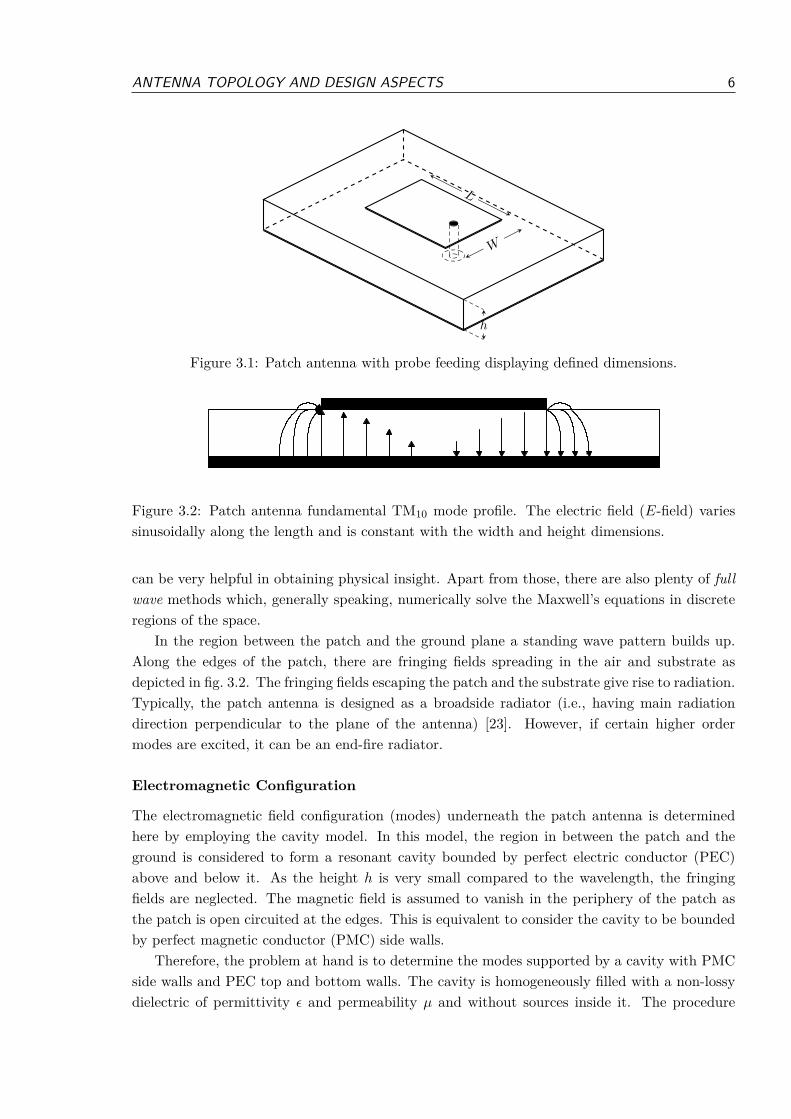
The patch antenna in its simplest form is shown in fig. 3.1, it consists of a rectangular metalstrip, i.e. the patch, of length L and width W (with L ≥ W ) located above a ground planeby a height h; which is typically much smaller than the wavelength. In between the patchand the ground plane, there is a dielectric substrate of permittivity ϵ. There are a couple ofpopular methods to feed the antenna (refer to section 3.1.3). On fig. 3.1 the coaxial or probefeed is represented; it is realized by soldering the center conductor of a coaxial cable to the patchwhereas the outer conductor is connected to the ground plane.
The most widespread methods used to analyze patch antennas are the transmission linemethod and the cavity model [23], [24]. These methods have limited accuracy and flexibility, but
5
ANTENNA TOPOLOGY AND DESIGN ASPECTS 6
W
L
h
Figure 3.1: Patch antenna with probe feeding displaying defined dimensions.
Figure 3.2: Patch antenna fundamental TM10 mode profile. The electric field (E-field) variessinusoidally along the length and is constant with the width and height dimensions.
can be very helpful in obtaining physical insight. Apart from those, there are also plenty of fullwave methods which, generally speaking, numerically solve the Maxwell’s equations in discreteregions of the space.
In the region between the patch and the ground plane a standing wave pattern builds up.Along the edges of the patch, there are fringing fields spreading in the air and substrate asdepicted in fig. 3.2. The fringing fields escaping the patch and the substrate give rise to radiation.Typically, the patch antenna is designed as a broadside radiator (i.e., having main radiationdirection perpendicular to the plane of the antenna) [23]. However, if certain higher ordermodes are excited, it can be an end-fire radiator.
Electromagnetic Configuration
The electromagnetic field configuration (modes) underneath the patch antenna is determinedhere by employing the cavity model. In this model, the region in between the patch and theground is considered to form a resonant cavity bounded by perfect electric conductor (PEC)above and below it. As the height h is very small compared to the wavelength, the fringingfields are neglected. The magnetic field is assumed to vanish in the periphery of the patch asthe patch is open circuited at the edges. This is equivalent to consider the cavity to be boundedby perfect magnetic conductor (PMC) side walls.
Therefore, the problem at hand is to determine the modes supported by a cavity with PMCside walls and PEC top and bottom walls. The cavity is homogeneously filled with a non-lossydielectric of permittivity ϵ and permeability µ and without sources inside it. The procedure
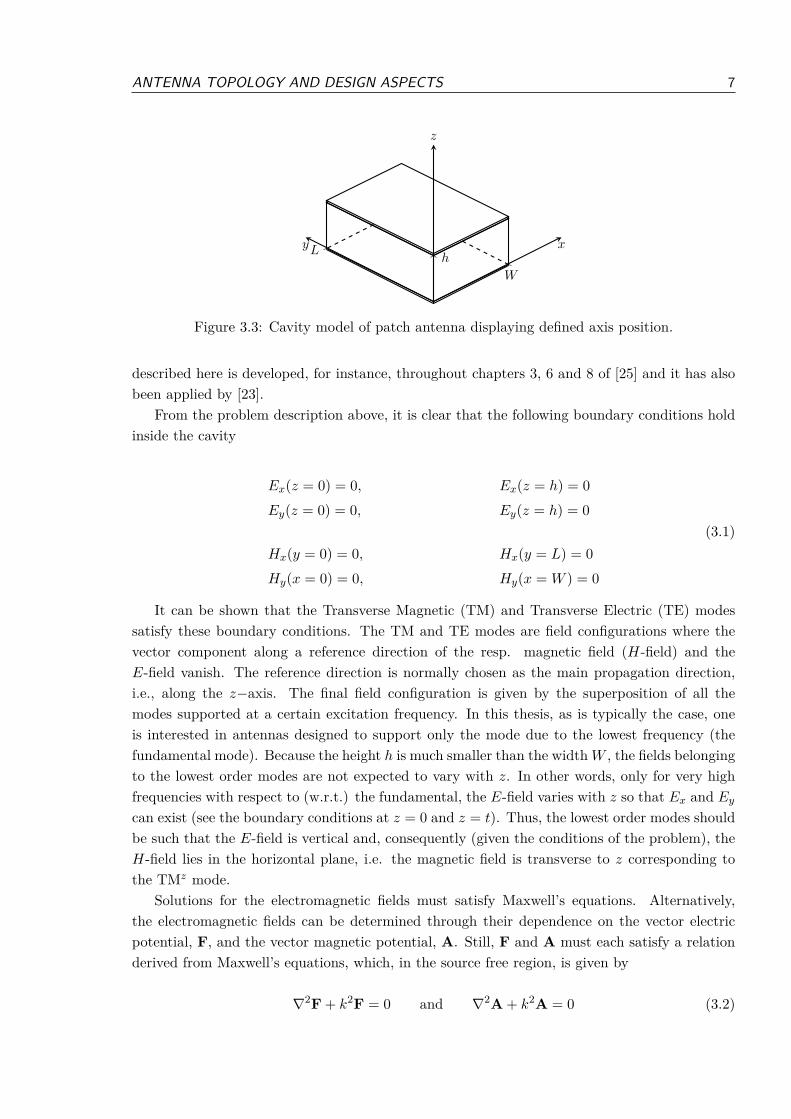
ANTENNA TOPOLOGY AND DESIGN ASPECTS 7
xy
z
L
W
h
Figure 3.3: Cavity model of patch antenna displaying defined axis position.
described here is developed, for instance, throughout chapters 3, 6 and 8 of [25] and it has alsobeen applied by [23].
From the problem description above, it is clear that the following boundary conditions holdinside the cavity
Ex(z = 0) = 0,
Ey(z = 0) = 0,
Hx(y = 0) = 0,
Hy(x = 0) = 0,
Ex(z = h) = 0
Ey(z = h) = 0
Hx(y = L) = 0
Hy(x = W ) = 0
(3.1)
It can be shown that the Transverse Magnetic (TM) and Transverse Electric (TE) modessatisfy these boundary conditions. The TM and TE modes are field configurations where thevector component along a reference direction of the resp. magnetic field (H-field) and theE-field vanish. The reference direction is normally chosen as the main propagation direction,i.e., along the z−axis. The final field configuration is given by the superposition of all themodes supported at a certain excitation frequency. In this thesis, as is typically the case, oneis interested in antennas designed to support only the mode due to the lowest frequency (thefundamental mode). Because the height h is much smaller than the width W , the fields belongingto the lowest order modes are not expected to vary with z. In other words, only for very highfrequencies with respect to (w.r.t.) the fundamental, the E-field varies with z so that Ex and Ey
can exist (see the boundary conditions at z = 0 and z = t). Thus, the lowest order modes shouldbe such that the E-field is vertical and, consequently (given the conditions of the problem), theH-field lies in the horizontal plane, i.e. the magnetic field is transverse to z corresponding tothe TMz mode.
Solutions for the electromagnetic fields must satisfy Maxwell’s equations. Alternatively,the electromagnetic fields can be determined through their dependence on the vector electricpotential, F, and the vector magnetic potential, A. Still, F and A must each satisfy a relationderived from Maxwell’s equations, which, in the source free region, is given by
∇2F+ k2F = 0 and ∇2A+ k2A = 0 (3.2)

ANTENNA TOPOLOGY AND DESIGN ASPECTS 8
where k is the phase constant and k2 = ω2µϵ. When computing the H-field from the vectorpotentials, one observes that when H is transverse to a certain direction, all components of Fand A must be zero, except for the component of A in that direction. So, for the TMz mode,it is enough to determine Az,
∇2Az + k2Az = 0 (3.3)
A general solution for Az can be found using the method of separation of variables. This iscarried out, for example, on chapter 3 of [25].
Az =f(x)g(y)h(z)
=[A1 cos(kxx) +B1 sin(kxx)][A2 cos(kyy) +B2 sin(kyy)]
.[A3 cos(kzz) +B3 sin(kzz)] (3.4)
The form of f(x), g(y) and h(z) is chosen to be sinusoidal because standing waves areexpected inside the cavity. The application of the separation of variables method also yields thefollowing relationship known as the constraint or dispersion equation.
k2x + k2y + k2z = k2 = ω2µϵ (3.5)
where kx, ky and kz are the components of k in the x, y and z directions. Now, the E-fieldand the H-field are related to the vector potentials by [25],
E = −jωA− j1
ωµϵ∇(∇ ·A)− 1
ϵ∇× F (3.6)
and
H =1
µ∇×A− jωF− j
1
ωµϵ∇(∇ · F) (3.7)
Substituting F = 0 and A = Azuz in eq. (3.6) and eq. (3.7), where uz is the unitary vectorin the z−direction,
Ex =− j1
ωµϵ
∂2Az
∂x∂z
Ey =− j1
ωµϵ
∂2Az
∂y∂z
Ez =− j1
ωµϵ
(∂2
∂z2+ k2
)Az
Hx =1
µ
∂Az
∂y
Hy = − 1
µ
∂Az
∂x
Hz = 0
(3.8)
By substituting eq. (3.4) in eqs. 3.8 and applying the boundary conditions (3.1), one findsthat B1, B2, B3 = 0. The product A0A1A2 is redefined as Amnn = A0A1A2. Then, Az
becomes,
Az = Amnp cos(kxx) cos(kyy) cos(kzz) (3.9)

ANTENNA TOPOLOGY AND DESIGN ASPECTS 9
with,
kx =mπ
W,
ky =nπ
L,
kz =pπ
h,
m = 0, 1, 2, ...
n = 0, 1, 2, ...
p = 0, 1, 2, ...
(3.10)
By introducing Az as given by eq. (3.9) in eqs. (3.8), the normalized electric and magneticfields are obtained as,
Ex = −jkxkzωµϵ
Amnp sin(kxx) cos(kyy) sin(kzz)
Ey = −jkykzωµϵ
Amnp cos(kxx) sin(kyy) sin(kzz)
Ez = −jk2 − k2zωµϵ
Amnp cos(kxx) cos(kyy) cos(kzz)
Hx =kyµAmnp cos(kxx) sin(kyy) cos(kzz)
Hy = −kxµAmnp sin(kxx) cos(kyy) cos(kzz)
Hz = 0
(3.11)
However, eqs. (3.11) are only valid when the constraint equation, (3.5), is satisfied. Thisgives rise to the modal resonant frequencies,
fmnp =1
2π√µϵ
√(mπ
W
)2+(nπL
)2+
(pπh
)2(3.12)
As L > W > h, the frequency of the fundamental mode (i.e., the lowest resonance frequency)is obtained from eq. (3.12) by setting m = 0, n = 1, p = 0,
f010 =1
2L√µϵ
=v
2L=⇒ L =
v
2f010=
λ010
2(3.13)
where v and λ010 are resp. the speed of light and the fundamental wavelength in the dielectricsubstrate. So L corresponds to half a wavelength of the fundamental resonating frequency inthe substrate medium. From eqs. 3.11, the fundamental TMz
010 mode is characterized by,
E010 = −E0 cos(πLy)uz and H010 = j
E0
Zcsin
(πLy)ux (3.14)
where E0 = jωA010 and Zc =
õ
ϵis the characteristic impedance in the dielectric substrate.
ANTENNA TOPOLOGY AND DESIGN ASPECTS 10
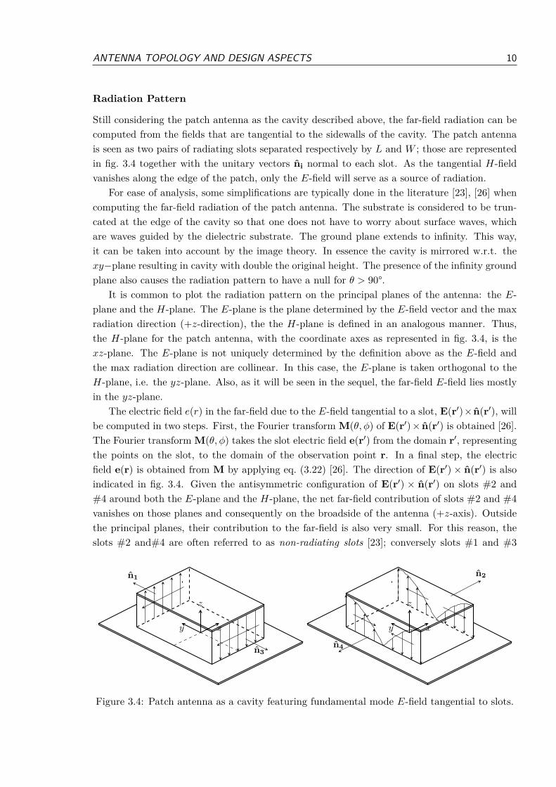
Radiation Pattern
Still considering the patch antenna as the cavity described above, the far-field radiation can becomputed from the fields that are tangential to the sidewalls of the cavity. The patch antennais seen as two pairs of radiating slots separated respectively by L and W ; those are representedin fig. 3.4 together with the unitary vectors ni normal to each slot. As the tangential H-fieldvanishes along the edge of the patch, only the E-field will serve as a source of radiation.
For ease of analysis, some simplifications are typically done in the literature [23], [26] whencomputing the far-field radiation of the patch antenna. The substrate is considered to be trun-cated at the edge of the cavity so that one does not have to worry about surface waves, whichare waves guided by the dielectric substrate. The ground plane extends to infinity. This way,it can be taken into account by the image theory. In essence the cavity is mirrored w.r.t. thexy−plane resulting in cavity with double the original height. The presence of the infinity groundplane also causes the radiation pattern to have a null for θ > 90°.
It is common to plot the radiation pattern on the principal planes of the antenna: the E-plane and the H-plane. The E-plane is the plane determined by the E-field vector and the maxradiation direction (+z-direction), the the H-plane is defined in an analogous manner. Thus,the H-plane for the patch antenna, with the coordinate axes as represented in fig. 3.4, is thexz-plane. The E-plane is not uniquely determined by the definition above as the E-field andthe max radiation direction are collinear. In this case, the E-plane is taken orthogonal to theH-plane, i.e. the yz-plane. Also, as it will be seen in the sequel, the far-field E-field lies mostlyin the yz-plane.
The electric field e(r) in the far-field due to the E-field tangential to a slot, E(r′)× n(r′), willbe computed in two steps. First, the Fourier transform M(θ, ϕ) of E(r′)× n(r′) is obtained [26].The Fourier transform M(θ, ϕ) takes the slot electric field e(r′) from the domain r′, representingthe points on the slot, to the domain of the observation point r. In a final step, the electricfield e(r) is obtained from M by applying eq. (3.22) [26]. The direction of E(r′)× n(r′) is alsoindicated in fig. 3.4. Given the antisymmetric configuration of E(r′) × n(r′) on slots #2 and#4 around both the E-plane and the H-plane, the net far-field contribution of slots #2 and #4vanishes on those planes and consequently on the broadside of the antenna (+z-axis). Outsidethe principal planes, their contribution to the far-field is also very small. For this reason, theslots #2 and#4 are often referred to as non-radiating slots [23]; conversely slots #1 and #3
xy
z
n1
n3
xy
z
n4
n2
Figure 3.4: Patch antenna as a cavity featuring fundamental mode E-field tangential to slots.

ANTENNA TOPOLOGY AND DESIGN ASPECTS 11
xy
z
H-planeE-plane
xy
z
ϕ
θ
Figure 3.5: Patch antenna showing its principal planes and coordinate system.
are mentioned as radiating slots. Here, the far-field generated by the non-radiating slots areneglected altogether.
In the coordinate position shown in fig. 3.4, the fundamental electric field in the cavity,eq. (3.14), becomes
E(r′) = E0 sin(πLy)uz (3.15)
Then the M -vector is calculated by the Fourier transform of E(r′)× n(r′) [26],
M(θ, ϕ) =ϵ
4π
∫Sa
E(r′)× n(r′)ejk.r′dS′ (3.16)
For slot #3
M1(θ, ϕ) = −uxϵ
4πE0e
−jkyL
2
∫ W2
−W2
ejkxx′dx′
∫ h
−hejkzz
′dz′
= −uxϵ
4π2E0Whe−j
kyL
2sin(X)
X
sin(Z)
Z(3.17)
(3.18)
Analogously,
M3(θ, ϕ) = −uxϵ
4π2E0Whe+j
kyL
2sin(X)
X
sin(Z)
Z(3.19)
So that,
M1(θ, ϕ) +M3(θ, ϕ) = −uxϵ
πE0Wh cos(Y )
sin(X)
X
sin(Z)
Z(3.20)
where,
X =kxW
2= k
W
2sin(θ) cos(ϕ)
Y =kyL
2= k
L
2sin(θ) sin(ϕ)
Z =kzh = kh cos(θ)
(3.21)
ANTENNA TOPOLOGY AND DESIGN ASPECTS 12
Note that the definition for kx, ky and kz implicit in eqs. (3.21) does not conflict either witheqs. (3.10) nor eq. (3.5).
e(r) ≈ e−jkr
rjωZcur × (M1(θ, ϕ) +M3(θ, ϕ)) (3.22)
In the E-plane (ϕ = 90°)
e(ϕ = 90°) = jE0Whk e−jkr
πrcos
(kL
2sin θ
)sin(kh cos θ)
kh cos θuθ (3.23)
In the H-plane (ϕ = 0°)
e(ϕ = 0°) = jE0Whk e−jkr
πr
sin(kW2 sin θ
)kW2 sin θ
sin(kh cos θ)
kh cos θcos θ uϕ (3.24)
where the last cos θ term in eq. (3.24) stems from the fact that ur in the E-plane iscos θ uz + sin θ ux
Equations (3.23) and (3.24) suggest that the antenna directivity increases with the dimen-sions L, W and h. This agrees with the property of Fourier transforms that states that givena transformation R′ 7→ R, the more limited the interval of the function defined in domain R′
is, the more expansive the transformation defined in domain R will be and vice-versa. Thetwo radiating slots of dimension L × h, can be seen as a linear antenna array of two elementsseparated by L. Thus, an increase in L, W or h represents a bigger support from the fields ofthe former domain, leading to a more contained (narrowbeam) far-field pattern.
Effective Length and Permittivity
In the previous derivation of the modes supported by the patch antenna using the cavity model,the fringing fields were neglected. The fields were considered to be confined to an homogeneousmedium of permittivity ϵ. For the fundamental mode, it was obtained that L = λ/2. In reality,the fringing fields cause the fundamental mode to extend outwards the patch [24]. So, L and W
should be replaced by the effective Lef and Wef , which are defined as
Lef = L+ 2∆L and Wef = W + 2∆W (3.25)
Since the fields are not only confined to the dielectric substrate but also spread trough theair, the configuration is inhomogeneous and it is not enough to assume the permittivity of themodes to be the one of the substrate material. One way to account for that while still using theequations derived with the cavity model, is to consider an effective permittivity, ϵef . The latter isessentially a weighted average permittivity of the air and the substrate material, which dependson the electromagnetic field configuration. As the frequency increases, the fields tend to get moreconfined to the substrate, whose permittivity is higher than the one of the air (ϵ0). An empiricalformula for calculating ϵef accounting for the frequency dependence is presented in Appendix Bof [24], but it is rather complex and gives little physical insight. Alternatively, a simpler but
ANTENNA TOPOLOGY AND DESIGN ASPECTS 13
less accurate approximation can be used to estimate the effective relative permittivity[23], [24],[26] ϵref ≡ ϵef
ϵ0,
ϵref ≈ϵr + 1
2+
ϵr − 1
2
[1 +
10h
W
]−1/2
(3.26)
where ϵr is the relative permittivity of the dielectric material, ϵr = ϵϵ0
. It is readily realized fromeq. (3.26) that ϵref is inversely related to h
W . The patch antenna becomes a better radiator whenits associated effective permittivity decreases. This is explained by the fact that the lower thepermittivity, the more field lines can scape the substrate, becoming a source of radiation.
An empirical approximation can also be used for ∆L when W ≫ h,
∆L ≈ h√ϵref
(3.27)
Bandwidth
Equation (3.12) suggests that the power spectrum density of the patch antenna has the formPSD = Pmnp δ(f−fmnp). Even though the patch antenna in its simplest form as depicted in thissection has indeed a very narrow bandwidth, the cavity model is just an approximation. Thebandwidth can be better estimated by considering the Q-factor, BW = 1
Q . The Q-factor is theratio of the energy stored to the energy lost (or scaped) from a resonant component. Therefore,in order to increase the BW of the patch antenna, one should make it a better radiator so thatmore field lines can scape the region underneath the patch.
3.1.2 Substrate Integrated Circuits
The cavity of the AFCBPA is based on the technological platform AFSIW. The AFSIW derivesfrom the Substrate-Integrated Waveguide (SIW) which was first introduced in [27] in the be-ginning of this century. Ever since its introduction, SIW has gained a lot of attention becausecontinuous efforts were devoted to connect traditional waveguide circuits to planar technologycircuits [28]. SIW allows to implement devices that have the functionalities of metallic rectan-gular waveguides using standard Printed Circuit Board (PCB) manufacturing processes. Morespecifically, in the SIW technique, a rectangular waveguide is integrated in a PCB by synthe-sizing its lateral walls with arrays of metalized via holes whereas its upper and lower walls arethe metal layers of the PCB [27], [29]. Because of the similarities to the traditional rectangularwaveguides the well-known design techniques can be applied [17] to map filters, antennas, phaseshifters, directional couples, mixers and oscillators etc [17], [18], [29], [30]. Transitions to otherplanar lines such as microstrip and Grounded Coplanar Waveguide (GCPW) have also beenproposed. The resulting SIW components inherit high-Q, low insertion loss and self shieldingcapabilities, which are typical for rectangular waveguide components; and, at the same time,are low profile, light weight, easy to integrate and relatively low cost [27]. The dielectric fill-ing (ϵr>1) makes the SIW components more compact in the plane of the substrate than theirtraditional waveguide counterparts, which are hollow inside. However, the presence of the lossy
ANTENNA TOPOLOGY AND DESIGN ASPECTS 14
dielectric and the array of vias, instead of a continuous wall, also reduces the Q-factor due to,respectively, the dielectric losses and the field leakage in between the vias.
Since the appearance of SIW, many variants were introduced aiming at specific purposes.Many of those technological platforms are mentioned in [29] and [28]. They receive the generalnomenclature SIC, encompassing all such techniques. One particular variant is the AFSIWfirst demonstrated in [17]. In the AFSIW fabrication process, a hole corresponding to thedimensions of the waveguide is milled from the substrate. This hole is metalized using a regularvia metalization process, representing the lateral walls of the waveguide. Extra (thin) PCBsare needed to make the top and bottom wall. The three PCBs are aligned by relying onalignment holes and they are either soldered or screwed together. Following this procedure, ahollow waveguide is created that has continuous metal walls instead of rows of vias. Thus, awaveguide built in AFSIW is larger, has higher Q-factor and lower insertion loss than its SIWcounterpart [17]. In many circumstances the larger device size can be a drawback; whereas atvery high frequencies when the wavelength becomes too small and problems with manufacturingtolerances arise, a technique that allows increasing the size of devices can be interesting. Thelower loss can be attributed to the absence of a lossy dielectric filling, no field leakage in betweenthe row of vias and reduced ohmic losses [18]. The latter is justified by considering that in thecase of AFSIW, the outer surface roughness of the copper foil has to be taken into account,whereas for SIW it is the inner surface roughness that matters. As the outer surface roughnessof the copper foil of a PCB is generally smaller than that of the inner surface, less ohmic lossesare to be expected [18], [31] in AFSIW.
It will be shown that thanks to the low losses experienced by the fields in a cavity built usingAFSIW technology, the AFCBPA achieves very high radiation efficiency.
3.1.3 Feeding
There are many popular ways of exciting the patch antenna. They can be classified into directand indirect methods depending whether there is a physical contact from the feed to the patchor not [23], [24]. Typically, indirect methods perform better in terms of bandwidth, spuriousradiation at the main beam direction and cross-polarized radiation [23]. Their main disadvantageis the need for a multi-layered structure which makes them less low-profile, more expensive andcomplex to fabricate. However, three PCBs are already necessary to create the air-filled cavityof the AFCBPA and this is in such a way that an indirect feeding method can be incorporatedwithout adding extra layers to the topology.
In fig. 3.6 (a), the aperture coupling is schematically represented. Three metal and twosubstrate layers are used. The patch is implemented on the top most metal layer and backedby the ground plane as usual. But in this case, there is a slot on the ground plane fromwhich the power conveyed by the feedline, at the bottommost layer, couples to the patch.Methods of analysis of the aperture coupling mechanism using the cavity method [32] and thetransmission line model [33] are available. The length of the feedline is such that it surpassesthe slot, essentially creating an open-circuited stub at its tip. By adjusting the size of thestub and the dimensions of the slot, the impedance bandwidth can be tunned. A multitudeof slot shapes have been reported in the literature [24], including the rectangular, the bowtie
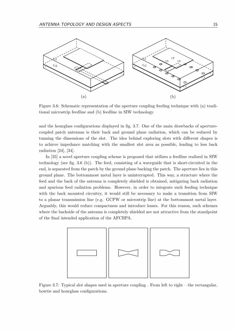
ANTENNA TOPOLOGY AND DESIGN ASPECTS 15
ϵr1ϵr2
(a)
ϵr1ϵr2
(b)
Figure 3.6: Schematic representation of the aperture coupling feeding technique with (a) tradi-tional microstrip feedline and (b) feedline in SIW technology.
and the hourglass configurations displayed in fig. 3.7. One of the main drawbacks of aperture-coupled patch antennas is their back and ground plane radiation, which can be reduced bytunning the dimensions of the slot. The idea behind exploring slots with different shapes isto achieve impedance matching with the smallest slot area as possible, leading to less backradiation [24], [34].
In [35] a novel aperture coupling scheme is proposed that utilizes a feedline realized in SIWtechnology (see fig. 3.6 (b)). The feed, consisting of a waveguide that is short-circuited in theend, is separated from the patch by the ground plane backing the patch. The aperture lies in thisground plane. The bottommost metal layer is uninterrupted. This way, a structure where thefeed and the back of the antenna is completely shielded is obtained, mitigating back radiationand spurious feed radiation problems. However, in order to integrate such feeding techniquewith the back mounted circuitry, it would still be necessary to make a transition from SIWto a planar transmission line (e.g. GCPW or microstrip line) at the bottommost metal layer.Arguably, this would reduce compactness and introduce losses. For this reason, such schemeswhere the backside of the antenna is completely shielded are not attractive from the standpointof the final intended application of the AFCBPA.
Figure 3.7: Typical slot shapes used in aperture coupling . From left to right – the rectangular,bowtie and hourglass configurations.
ANTENNA TOPOLOGY AND DESIGN ASPECTS 16
The substrate underneath the patch can be chosen independently of that of the feedline.This way, the former can be selected thicker and with ϵr1 lower than ϵr2 of the latter allowingfor separate optimization of, in one hand, the radiation from the patch and, on the other hand,the feedline spurious radiation suppression [23], [24], [34].
3.2 Air-Filled Cavity Backed Patch Antenna
In this section the proposed AFCBPA is presented. Its topology was put together in order toachieve certain goals; and it is based on notions expressed by the theory elucidated above andon previously reported prototypes [18], [36]. Those goals, as discussed in chapter 2, are:
• 3-dB beamwidth ≈ 70°
• FTBR > 10 dB
• Efficiency η > 90%
• S11 < −10 dB in system band 27.5GHz to 29.5 GHz.
• Easy of mounting electronics on the backside
• Suited for array incorporation
suppress surface wave
fit in an array with d = 0.64λ0 = 6.45mm
On top of covering the system band, achieving larger BW is desired. It would make theantenna attractive to be reused in future projects. The functional size of the AFCBPA isdetermined by the size of its cavity, which is its largest feature. According to the design rule ofthe PCB manufacturer Eurocircuits, two of those cavities can be placed aside when a clearanceof 0.5 mm is respected. In this case, the AFCBPA should be smaller than 5.95mm.
The exploded view of the antenna topology is shown in fig. 3.8. The AFCBPA is an aperturecoupled patch antenna whose patch lies over an air cavity. It consists of 3 stacked PCBs, whichare referred to as – from top to bottom of fig. 3.8 – PCB3, PCB2 and PCB1. A GCPW feedlineis etched on the metal layer of PCB3 displayed on top of fig. 3.8 (a). The opposite metal layer ofPCB3 – not evident from fig. 3.8 (a) – is the ground plane of the patch antenna. It contains thehourglass shaped slot which is part of the aperture coupling feeding arrangement (see fig. 3.9).This ground plane and that of the GCPW are connected through regularly spaced vias. Notefrom fig. 3.9 that opposite to the hourglass aperture, there is a rectangular slot on the GCPWground plane. If this slot was not there, keeping in mind that the height between the GCPWground plane and the coupling aperture is very small compared to λ, then the tangential fieldsat the coupling aperture would be fairly attenuated. The air-filled cavity in AFSIW technologyis milled away from PCB2 and the side walls are electro-plated as described in section 3.1.2 andshown in fig. 3.8 (b). Finally, the patch is etched on the metal layer of PCB1 shown on top offig. 3.8 (c); on the opposite side of PCB1 there is no metal layer.
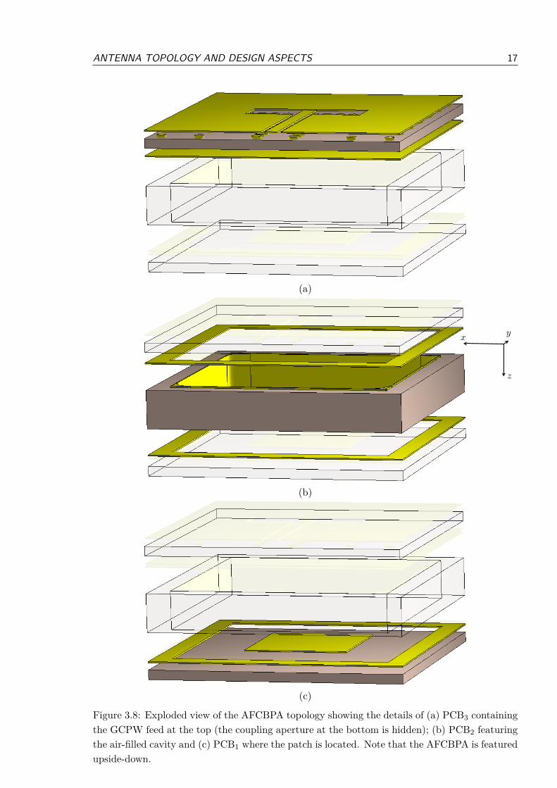
ANTENNA TOPOLOGY AND DESIGN ASPECTS 17
(a)
(b)
(c)
xy
z
Figure 3.8: Exploded view of the AFCBPA topology showing the details of (a) PCB3 containingthe GCPW feed at the top (the coupling aperture at the bottom is hidden); (b) PCB2 featuringthe air-filled cavity and (c) PCB1 where the patch is located. Note that the AFCBPA is featuredupside-down.
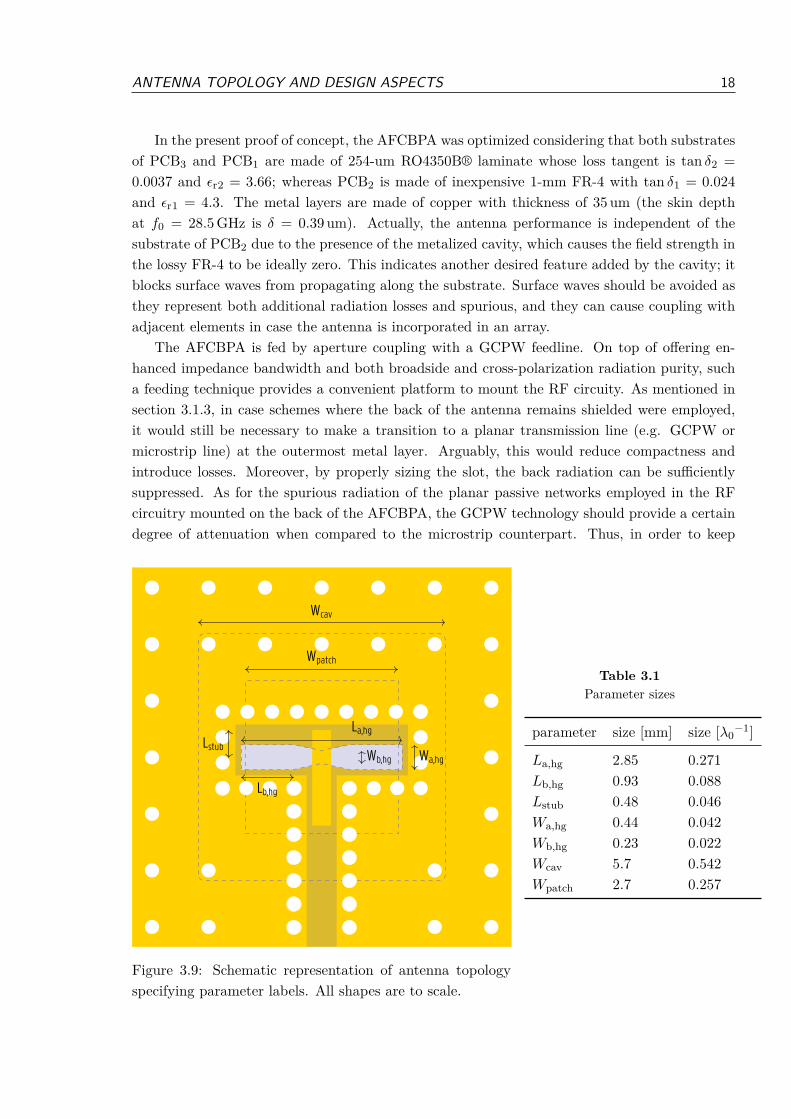
ANTENNA TOPOLOGY AND DESIGN ASPECTS 18
In the present proof of concept, the AFCBPA was optimized considering that both substratesof PCB3 and PCB1 are made of 254-um RO4350B® laminate whose loss tangent is tan δ2 =
0.0037 and ϵr2 = 3.66; whereas PCB2 is made of inexpensive 1-mm FR-4 with tan δ1 = 0.024
and ϵr1 = 4.3. The metal layers are made of copper with thickness of 35 um (the skin depthat f0 = 28.5GHz is δ = 0.39 um). Actually, the antenna performance is independent of thesubstrate of PCB2 due to the presence of the metalized cavity, which causes the field strength inthe lossy FR-4 to be ideally zero. This indicates another desired feature added by the cavity; itblocks surface waves from propagating along the substrate. Surface waves should be avoided asthey represent both additional radiation losses and spurious, and they can cause coupling withadjacent elements in case the antenna is incorporated in an array.
The AFCBPA is fed by aperture coupling with a GCPW feedline. On top of offering en-hanced impedance bandwidth and both broadside and cross-polarization radiation purity, sucha feeding technique provides a convenient platform to mount the RF circuity. As mentioned insection 3.1.3, in case schemes where the back of the antenna remains shielded were employed,it would still be necessary to make a transition to a planar transmission line (e.g. GCPW ormicrostrip line) at the outermost metal layer. Arguably, this would reduce compactness andintroduce losses. Moreover, by properly sizing the slot, the back radiation can be sufficientlysuppressed. As for the spurious radiation of the planar passive networks employed in the RFcircuitry mounted on the back of the AFCBPA, the GCPW technology should provide a certaindegree of attenuation when compared to the microstrip counterpart. Thus, in order to keep
La,hg
Wa,hgWb,hgLstub
Lb,hg
Wpatch
Wcav
Figure 3.9: Schematic representation of antenna topologyspecifying parameter labels. All shapes are to scale.
Table 3.1Parameter sizes
parameter size [mm] size [λ0−1]
La,hg 2.85 0.271Lb,hg 0.93 0.088Lstub 0.48 0.046Wa,hg 0.44 0.042Wb,hg 0.23 0.022Wcav 5.7 0.542Wpatch 2.7 0.257
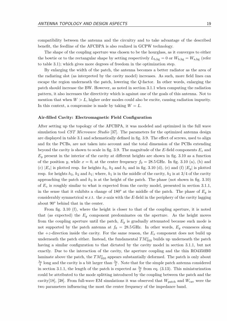
ANTENNA TOPOLOGY AND DESIGN ASPECTS 19
compatibility between the antenna and the circuitry and to take advantage of the describedbenefit, the feedline of the AFCBPA is also realized in GCPW technology.
The shape of the coupling aperture was chosen to be the hourglass, as it converges to eitherthe bowtie or to the rectangular shape by setting respectively Lb,hg = 0 or Wb,hg = Wa,hg (referto table 3.1); which gives more degrees of freedom in the optimization step.
By enlarging the width of the patch, the antenna becomes a better radiator as the area ofthe radiating slot (as interpreted by the cavity model) increases. As such, more field lines canescape the region underneath the patch, lowering the Q-factor. In other words, enlarging thepatch should increase the BW. However, as noted in section 3.1.1 when computing the radiationpattern, it also increases the directivity which is against one of the goals of this antenna. Not tomention that when W > L, higher order modes could also be excite, causing radiation impurity.In this context, a compromise is made by taking W = L.
Air-filled Cavity: Electromagnetic Field Configuration
After setting up the topology of the AFCBPA, it was modeled and optimized in the full wavesimulation tool CST Microwave Studio [37]. The parameters for the optimized antenna designare displayed in table 3.1 and schematically defined in fig. 3.9. The effect of screws, used to alignand fix the PCBs, are not taken into account and the total dimension of the PCBs extendingbeyond the cavity is shown to scale in fig. 3.9. The magnitude of the E-field components Ez andEy present in the interior of the cavity at different heights are shown in fig. 3.10 as a functionof the position y, while x = 0, at the center frequency f0 = 28.5GHz. In fig. 3.10 (a), (b) and(c) |Ez| is plotted resp. for heights h3, h2 and h1 and in fig. 3.10 (d), (e) and (f) |Ey| is plottedresp. for heights h3, h2 and h1; where, h1 is in the middle of the cavity, h2 is at 3/4 of the cavityapproaching the patch and h3 is at the height of the patch. The phase (not shown in fig. 3.10)of Ez is roughly similar to what is expected from the cavity model, presented in section 3.1.1,in the sense that it exhibits a change of 180° at the middle of the patch. The phase of Ey isconsiderably symmetrical w.r.t. the x-axis with the E-field in the periphery of the cavity laggingabout 90° behind that in the center.
From fig. 3.10 (f), where the height is closer to that of the coupling aperture, it is notedthat (as expected) the Ey component predominates on the aperture. As the height movesfrom the coupling aperture until the patch, Ey is gradually attenuated because such mode isnot supported by the patch antenna at f0 = 28.5GHz. In other words, Ey evanesces alongthe +z-direction inside the cavity. For the same reason, the Ex component does not build upunderneath the patch either. Instead, the fundamental TM z
010 builds up underneath the patchhaving a similar configuration to that dictated by the cavity model in section 3.1.1, but notexactly. Due to the interaction of the cavity, the aperture coupling and the thin RO4350B®laminate above the patch, the TM z
010 appears substantially deformed. The patch is only aboutλ04 long and the cavity is a bit larger than λ0
2 . Note that for the simple patch antenna consideredin section 3.1.1, the length of the patch is expected as λ0
2 from eq. (3.13). This miniaturizationcould be attributed to the mode splitting introduced by the coupling between the patch and thecavity[18], [38]. From full-wave EM simulations it was observed that Wpatch and Wcav were thetwo parameters influencing the most the center frequency of the impedance band.
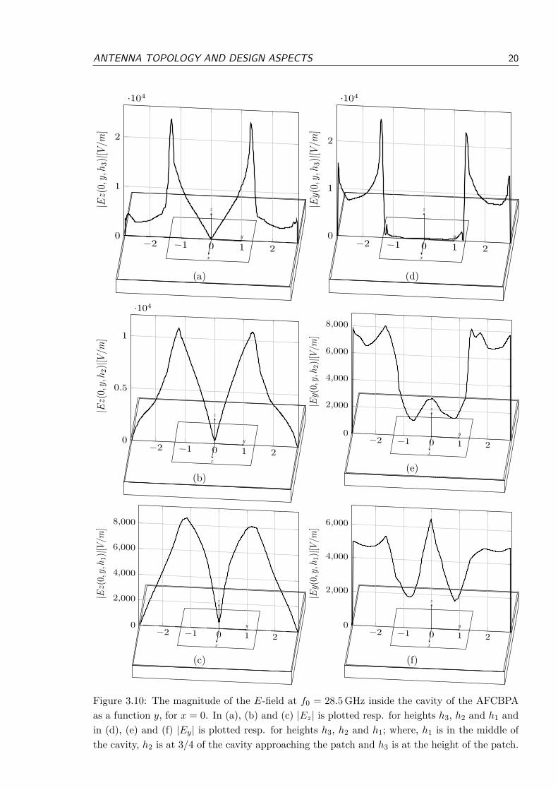
ANTENNA TOPOLOGY AND DESIGN ASPECTS 20
−2 −1 0 1 2
0
1
2
·104|E
z(0,y,h 3
)|[V/m
]
x
y
z
(a)
−2 −1 0 1 2
0
1
2
·104
|Ey(0,y,h 3
)|[V/m
]
x
y
z
(d)
−2 −1 0 1 2
0
0.5
1
·104
|Ez(0,y,h 2
)|[V/m
]
x
y
z
(b)
−2 −1 0 1 2
0
2,000
4,000
6,000
8,000
|Ey(0,y,h 2
)|[V/m
]
x
y
z
(e)
−2 −1 0 1 2
0
2,000
4,000
6,000
8,000
|Ez(0,y,h 1
)|[V/m
]
x
y
z
(c)
−2 −1 0 1 2
0
2,000
4,000
6,000
|Ey(0,y,h 1
)|[V/m
]
x
y
z
(f)
Figure 3.10: The magnitude of the E-field at f0 = 28.5GHz inside the cavity of the AFCBPAas a function y, for x = 0. In (a), (b) and (c) |Ez| is plotted resp. for heights h3, h2 and h1 andin (d), (e) and (f) |Ey| is plotted resp. for heights h3, h2 and h1; where, h1 is in the middle ofthe cavity, h2 is at 3/4 of the cavity approaching the patch and h3 is at the height of the patch.
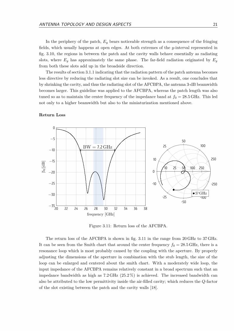
ANTENNA TOPOLOGY AND DESIGN ASPECTS 21
In the periphery of the patch, Ey bears noticeable strength as a consequence of the fringingfields, which usually happens at open edges. At both extremes of the y-interval represented infig. 3.10, the regions in between the patch and the cavity walls behave essentially as radiatingslots, where Ey has approximately the same phase. The far-field radiation originated by Ey
from both these slots add up in the broadside direction.The results of section 3.1.1 indicating that the radiation pattern of the patch antenna becomes
less directive by reducing the radiating slot size can be invoked. As a result, one concludes thatby shrinking the cavity, and thus the radiating slot of the AFCBPA, the antenna 3-dB beamwidthbecomes larger. This guideline was applied to the AFCBPA, whereas the patch length was alsotuned so as to maintain the center frequency of the impedance band at f0 = 28.5GHz. This lednot only to a higher beamwidth but also to the miniaturization mentioned above.
Return Loss
20 22 24 26 28 30 32 34 36 38−35
−30
−25
−20
−15
−10
−5
0
BW = 7.2GHz
frequency [GHz]
|S 11|[dB
]
10 25 50 100 2500
10
2550
100
250
-10
-25-50
-100
-250
37GHz
Figure 3.11: Return loss of the AFCBPA.
The return loss of the AFCBPA is shown in fig. 3.11 in the range from 20GHz to 37GHz.It can be seen from the Smith chart that around the center frequency f0 = 28.5GHz, there is aresonance loop which is most probably caused by the coupling with the aperture. By properlyadjusting the dimensions of the aperture in combination with the stub length, the size of theloop can be enlarged and centered about the smith chart. With a moderately wide loop, theinput impedance of the AFCBPA remains relatively constant in a broad spectrum such that animpedance bandwidth as high as 7.2 GHz (25.2 %) is achieved. The increased bandwidth canalso be attributed to the low permittivity inside the air-filled cavity; which reduces the Q-factorof the slot existing between the patch and the cavity walls [18].
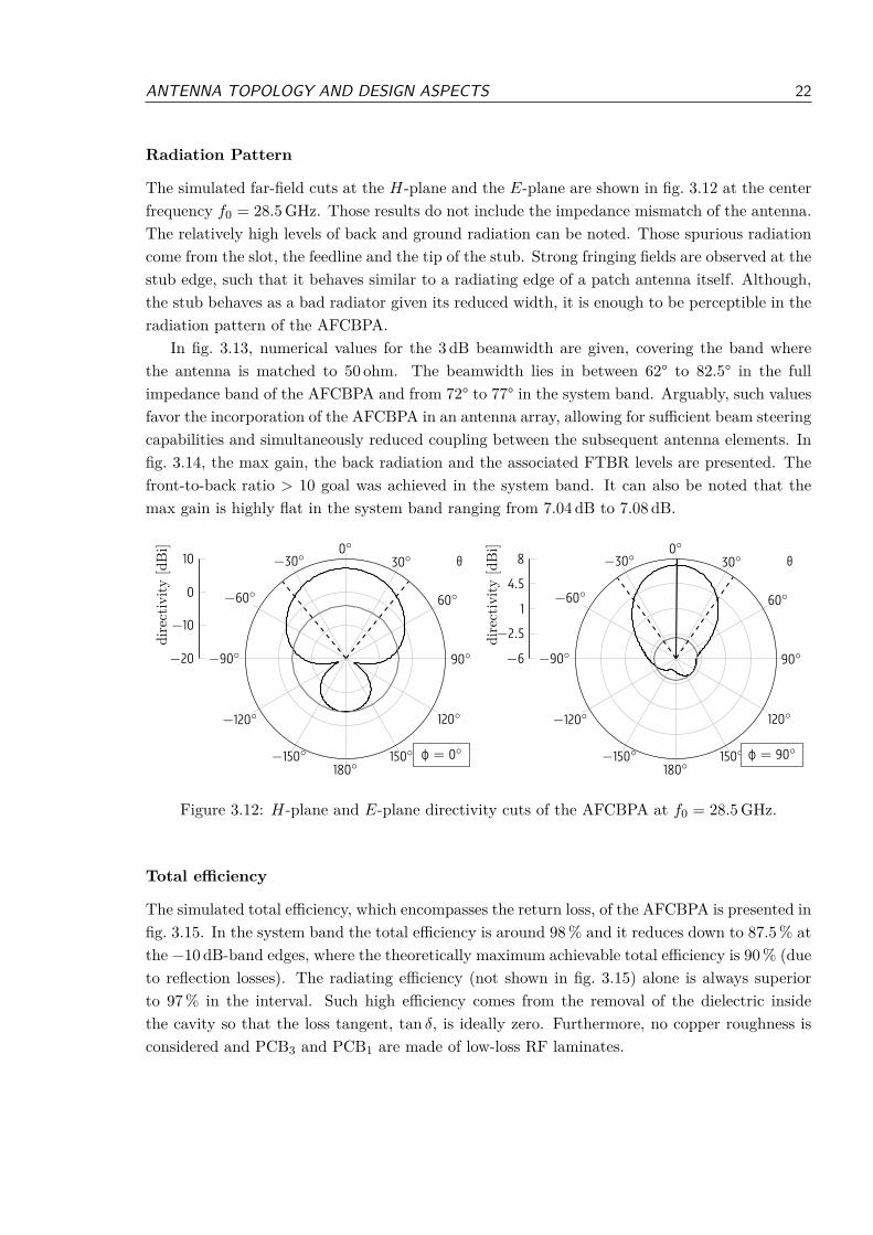
ANTENNA TOPOLOGY AND DESIGN ASPECTS 22
Radiation Pattern
The simulated far-field cuts at the H-plane and the E-plane are shown in fig. 3.12 at the centerfrequency f0 = 28.5GHz. Those results do not include the impedance mismatch of the antenna.The relatively high levels of back and ground radiation can be noted. Those spurious radiationcome from the slot, the feedline and the tip of the stub. Strong fringing fields are observed at thestub edge, such that it behaves similar to a radiating edge of a patch antenna itself. Although,the stub behaves as a bad radiator given its reduced width, it is enough to be perceptible in theradiation pattern of the AFCBPA.
In fig. 3.13, numerical values for the 3 dB beamwidth are given, covering the band wherethe antenna is matched to 50 ohm. The beamwidth lies in between 62° to 82.5° in the fullimpedance band of the AFCBPA and from 72° to 77° in the system band. Arguably, such valuesfavor the incorporation of the AFCBPA in an antenna array, allowing for sufficient beam steeringcapabilities and simultaneously reduced coupling between the subsequent antenna elements. Infig. 3.14, the max gain, the back radiation and the associated FTBR levels are presented. Thefront-to-back ratio > 10 goal was achieved in the system band. It can also be noted that themax gain is highly flat in the system band ranging from 7.04 dB to 7.08 dB.
030
60
90
120
150180
−150
−120
−90
−60
−30
−20
−10
0
10 θ
dire
ctiv
ity[dBi]
φ = 0
030
60
90
120
150180
−150
−120
−90
−60
−30
−6
−2.51
4.5
8 θ
dire
ctiv
ity[dBi]
φ = 90
Figure 3.12: H-plane and E-plane directivity cuts of the AFCBPA at f0 = 28.5GHz.
Total efficiency
The simulated total efficiency, which encompasses the return loss, of the AFCBPA is presented infig. 3.15. In the system band the total efficiency is around 98 % and it reduces down to 87.5 % atthe −10 dB-band edges, where the theoretically maximum achievable total efficiency is 90 % (dueto reflection losses). The radiating efficiency (not shown in fig. 3.15) alone is always superiorto 97 % in the interval. Such high efficiency comes from the removal of the dielectric insidethe cavity so that the loss tangent, tan δ, is ideally zero. Furthermore, no copper roughness isconsidered and PCB3 and PCB1 are made of low-loss RF laminates.
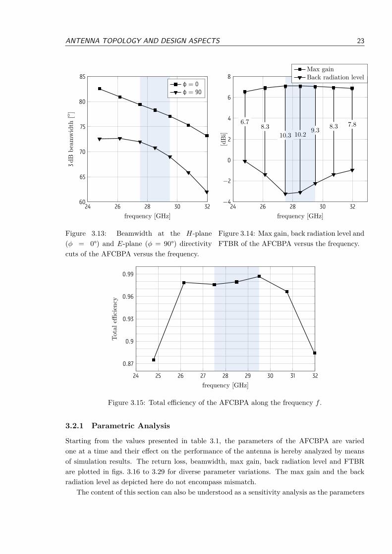
ANTENNA TOPOLOGY AND DESIGN ASPECTS 23
24 26 28 30 3260
65
70
75
80
85
frequency [GHz]
3dB
beam
wid
th[o ]
φ = 0φ = 90
Figure 3.13: Beamwidth at the H-plane(ϕ = 0°) and E-plane (ϕ = 90°) directivitycuts of the AFCBPA versus the frequency.
24 26 28 30 32−4
−2
0
2
4
6
8
6.78.3
10.3 10.2 9.3 8.3 7.8
frequency [GHz][dBi]
Max gainBack radiation level
Figure 3.14: Max gain, back radiation level andFTBR of the AFCBPA versus the frequency.
24 25 26 27 28 29 30 31 32
0.87
0.9
0.93
0.96
0.99
frequency [GHz]
Tota
leffi
cien
cy
Figure 3.15: Total efficiency of the AFCBPA along the frequency f .
3.2.1 Parametric Analysis
Starting from the values presented in table 3.1, the parameters of the AFCBPA are variedone at a time and their effect on the performance of the antenna is hereby analyzed by meansof simulation results. The return loss, beamwidth, max gain, back radiation level and FTBRare plotted in figs. 3.16 to 3.29 for diverse parameter variations. The max gain and the backradiation level as depicted here do not encompass mismatch.
The content of this section can also be understood as a sensitivity analysis as the parameters
ANTENNA TOPOLOGY AND DESIGN ASPECTS 24
are varied within a span that at least covers the manufacturing tolerances. However, the mainpurpose is to give an idea of the role of each parameter on the process of tunning the design. Inthis sense, the author aims to report his experiences in optimizing the AFCBPA so as to providea starting point for anyone willing to use it in an eventual future work.
Effect of Lstub
The Lstub is the most sensitive parameter of the antenna in terms of impedance matching.When it is varied just by ±50 um, which corresponds to the manufacturing tolerance providedby Eurocircuits, it already causes a substantial change on the locus of the S11 on the smith chart(fig. 3.16). From the smith chart, it is observed that by increasing Lstub, the lower frequencyend splits apart from the higher frequency end (marked with the symbol: ‘•’). In general,proper tunning of this parameter is paramount to bring the loop to the center of the smith chartbecause it is the main responsible for translating the loop in the radial direction. When, Lstub isconsiderably larger than the default chosen value (48 um), the other parameters analyzed mainlyrotate the loop without bringing it sufficiently close to the center.
Lstub does not play any center hole in the beamwidth nor in the max gain - because the stubis on the back of the antenna - but it can persistently be observed that it does affect the backradiation level (see fig. 3.17). Generally, by increasing Lstub in the vicinity of its default value,the back radiation level decreases.
Effect of Aperture Parameters
The parameters La,hg, Wa,hg, Wb,hg and Lb,hg generally cause the loop of the S11 curve (see theplot on the smith chart) to enlarge while moving towards the higher frequency end (markedwith the symbol: ‘•’). The former two parameters present a direct relation and the latter twoare inversely related to these effects. So, by collectively tunning these parameters, also witha proper choice for Lstub, the loop can be brought to the center with a sufficient loop area toachieve the desired BW.
It is interesting that when the length, La,hg, and the with, Wa,hg, of the aperture increases,the back radiation level decreases. This trend was persistently observed for La,hg and Wa,hg andthat is why the default values of these parameters were set relatively high (e.g. La,hg is greaterthan the patch width). It is also noted that when the hourglass tends to a rectangular shape,i.e. by increasing Wb,hg and Lb,hg, the back radiation worsens.
Effect of Wcav
The Wcav parameter dictates the cavity size and thus the size of the equivalent slot existing in theregion in between the patch and the walls of the cavity. It can be seen from fig. 3.26 that Wcavis inversely related to the loop area such that shrinking the slot of AFCBPA can potentiallyincrease its BW. When just a patch antenna in its simplest form is concerned, this relationhappens in the opposite way i.e., the slot size (width × height of the substrate) of the simplepatch antenna is directly related to the bandwidth because the greater the slot the more field

ANTENNA TOPOLOGY AND DESIGN ASPECTS 25
lines can scape, which reduces the Q-factor. However, for the AFCBPA, this is more complexand the interaction with the feeding scheme and the cavity has to be taken into account.
As the equivalent radiating slot of the AFCBPA shrinks, the beamwidth increases as expected(see fig. 3.27). This also means a smaller max gain. At the same time, the side lobe that canbe observed on the E-plane in fig. 3.12 at around θ = 120° enlarges. Consequently, the FTBRbecomes lower.
Effect of Wpatch
The parameter Wpatch, representing the patch width, is now altered in increments of 100 um.The effect on the return loss of the AFCBPA is plotted in fig. 3.28 where the frequency f0 =
28.5GHz is marked with the symbol ‘’ on the smith chart. A change in Wpatch makes the pointcorresponding to f0 in the Smith chart to move around the resonance loop. No other parameterproduces this effect at such a rate.
A frequency shift is also observed on the results related to the directivity in fig. 3.29.
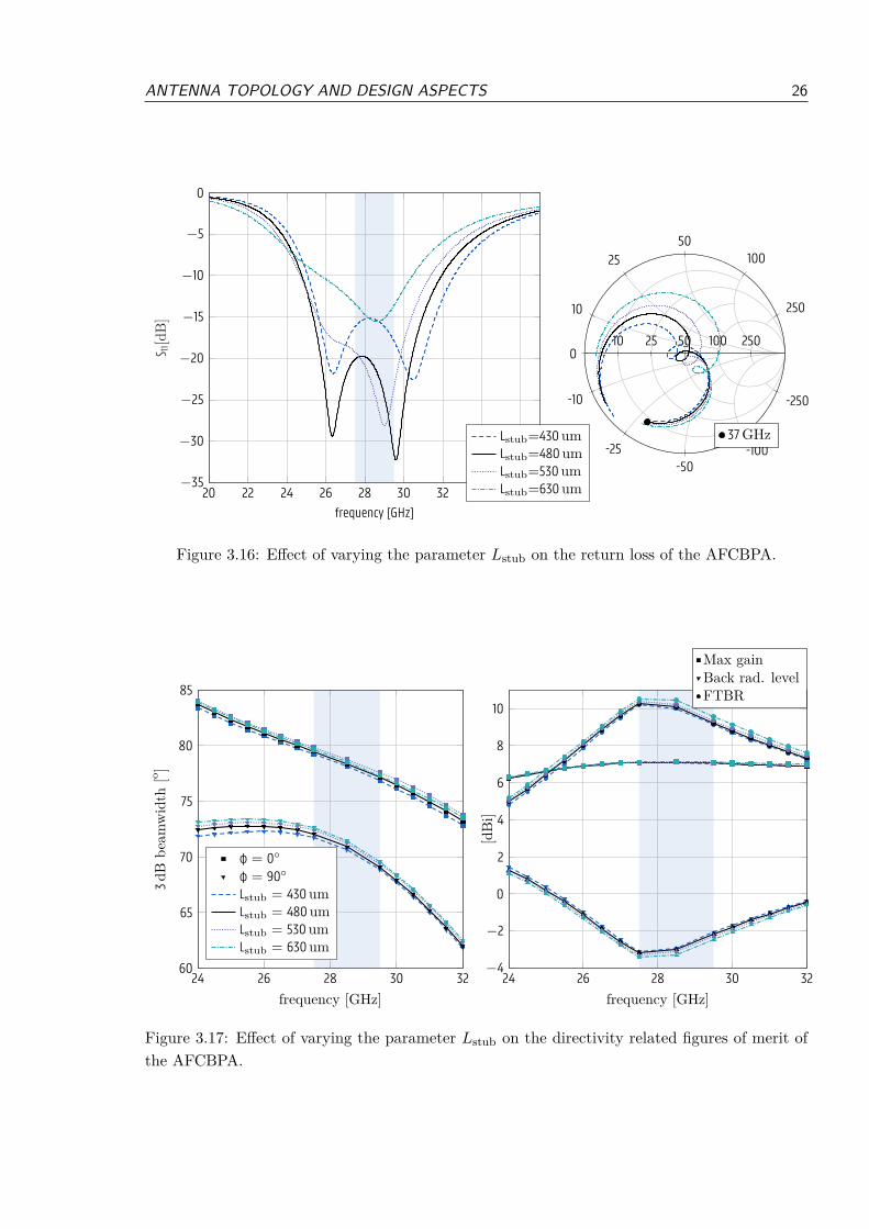
ANTENNA TOPOLOGY AND DESIGN ASPECTS 26
20 22 24 26 28 30 32 34 36−35
−30
−25
−20
−15
−10
−5
0
frequency [GHz]
S 11[dB
]
Lstub=430umLstub=480umLstub=530 umLstub=630um
10 25 50 100 2500
10
2550
100
250
-10
-25-50
-100
-250
37GHz
Figure 3.16: Effect of varying the parameter Lstub on the return loss of the AFCBPA.
24 26 28 30 3260
65
70
75
80
85
frequency [GHz]
3dB
beam
wid
th[o ]
φ = 0
φ = 90
Lstub = 430umLstub = 480umLstub = 530umLstub = 630um
24 26 28 30 32−4
−2
0
2
4
6
8
10
frequency [GHz]
[dBi]
Max gainBack rad. levelFTBR
Figure 3.17: Effect of varying the parameter Lstub on the directivity related figures of merit ofthe AFCBPA.
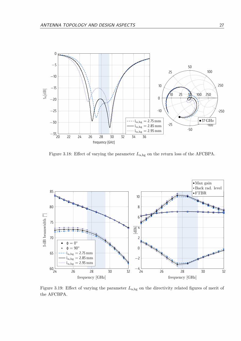
ANTENNA TOPOLOGY AND DESIGN ASPECTS 27
20 22 24 26 28 30 32 34 36−35
−30
−25
−20
−15
−10
−5
0
frequency [GHz]
S 11[dB
]
La,hg = 2.75mmLa,hg = 2.85mmLa,hg = 2.95mm
10 25 50 100 2500
10
2550
100
250
-10
-25-50
-100
-250
37GHz
Figure 3.18: Effect of varying the parameter La,hg on the return loss of the AFCBPA.
24 26 28 30 3260
65
70
75
80
85
frequency [GHz]
3dB
beam
wid
th[o ]
φ = 0
φ = 90
La,hg = 2.75mmLa,hg = 2.85mmLa,hg = 2.95mm
24 26 28 30 32−4
−2
0
2
4
6
8
10
frequency [GHz]
[dBi]
Max gainBack rad. levelFTBR
Figure 3.19: Effect of varying the parameter La,hg on the directivity related figures of merit ofthe AFCBPA.
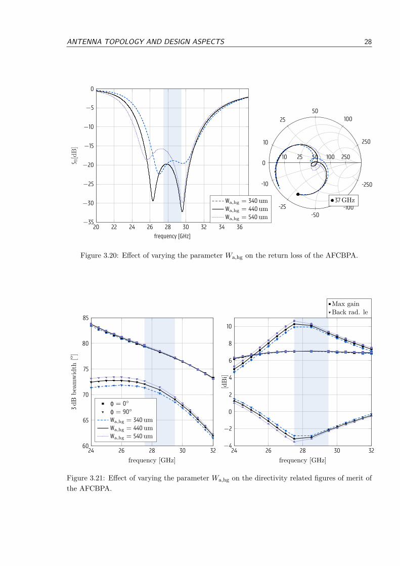
ANTENNA TOPOLOGY AND DESIGN ASPECTS 28
20 22 24 26 28 30 32 34 36−35
−30
−25
−20
−15
−10
−5
0
frequency [GHz]
S 11[dB
]
Wa,hg = 340umWa,hg = 440 umWa,hg = 540 um
10 25 50 100 2500
10
2550
100
250
-10
-25-50
-100
-250
37GHz
Figure 3.20: Effect of varying the parameter Wa,hg on the return loss of the AFCBPA.
24 26 28 30 3260
65
70
75
80
85
frequency [GHz]
3dB
beam
wid
th[o ]
φ = 0
φ = 90
Wa,hg = 340umWa,hg = 440umWa,hg = 540um
24 26 28 30 32−4
−2
0
2
4
6
8
10
frequency [GHz]
[dBi]
Max gainBack rad. le
Figure 3.21: Effect of varying the parameter Wa,hg on the directivity related figures of merit ofthe AFCBPA.

ANTENNA TOPOLOGY AND DESIGN ASPECTS 29
20 22 24 26 28 30 32 34 36−35
−30
−25
−20
−15
−10
−5
0
frequency [GHz]
S 11[dB
]
Wb,hg = 130umWb,hg = 230umWb,hg = 330um
10 25 50 100 2500
10
2550
100
250
-10
-25-50
-100
-250
37GHz
Figure 3.22: Effect of varying the parameter Wb,hg on the return loss of the AFCBPA.
24 26 28 30 3260
65
70
75
80
85
frequency [GHz]
3dB
beam
wid
th[o ]
φ = 0
φ = 90
Wb,hg = 130 umWb,hg = 230umWb,hg = 330 um
24 26 28 30 32−4
−2
0
2
4
6
8
10
frequency [GHz]
[dBi]
Max gainBack rad. levelFTBR
Figure 3.23: Effect of varying the parameter Wb,hg on the directivity related figures of merit ofthe AFCBPA.
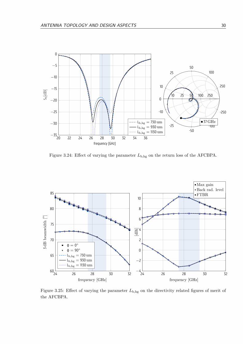
ANTENNA TOPOLOGY AND DESIGN ASPECTS 30
20 22 24 26 28 30 32 34 36−35
−30
−25
−20
−15
−10
−5
0
frequency [GHz]
S 11[dB
]
Lb,hg = 730 umLb,hg = 930 umLb,hg = 1130um
10 25 50 100 2500
10
2550
100
250
-10
-25-50
-100
-250
37GHz
Figure 3.24: Effect of varying the parameter Lb,hg on the return loss of the AFCBPA.
24 26 28 30 3260
65
70
75
80
85
frequency [GHz]
3dB
beam
wid
th[o ]
φ = 0
φ = 90
Lb,hg = 730 umLb,hg = 930umLb,hg = 1130um
24 26 28 30 32−4
−2
0
2
4
6
8
10
frequency [GHz]
[dBi]
Max gainBack rad. levelFTBR
Figure 3.25: Effect of varying the parameter Lb,hg on the directivity related figures of merit ofthe AFCBPA.
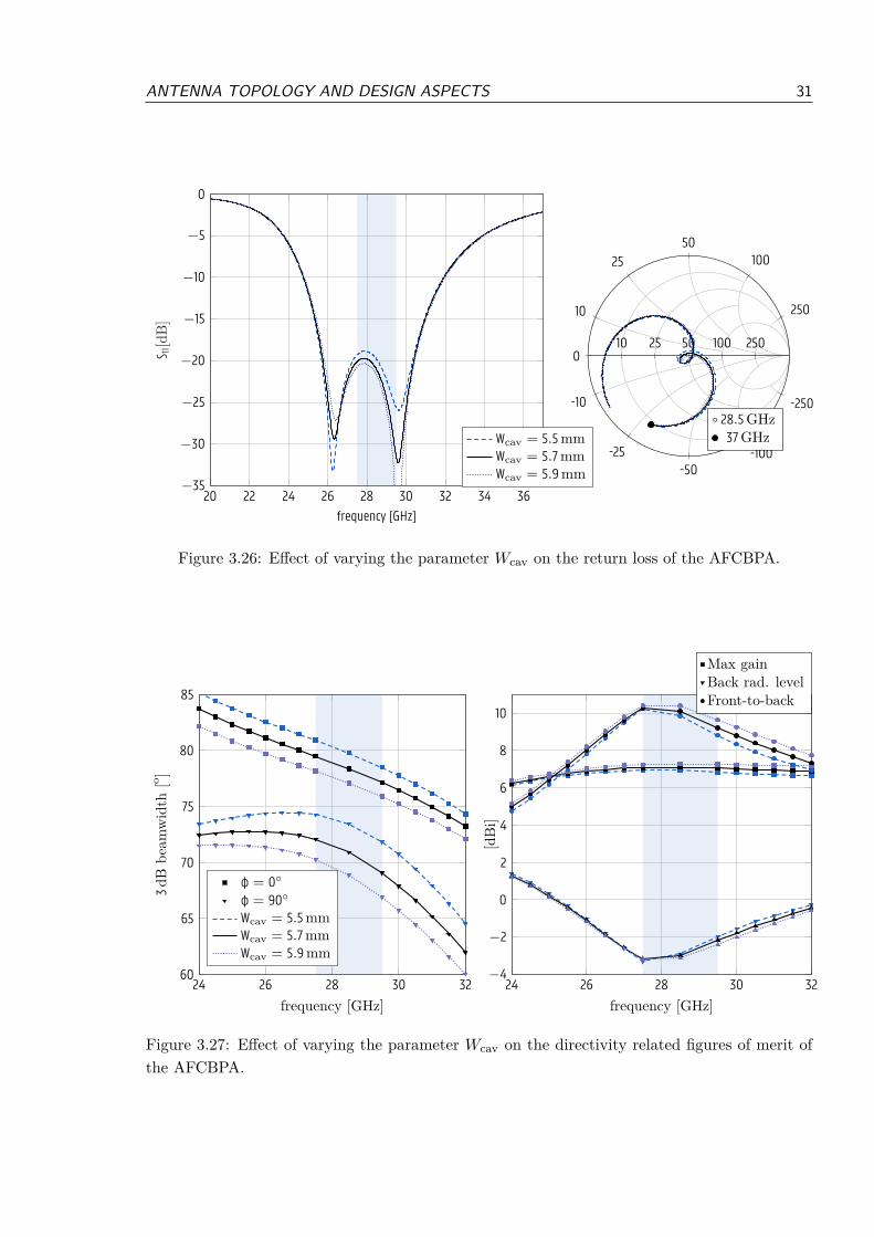
ANTENNA TOPOLOGY AND DESIGN ASPECTS 31
20 22 24 26 28 30 32 34 36−35
−30
−25
−20
−15
−10
−5
0
frequency [GHz]
S 11[dB
]
Wcav = 5.5mmWcav = 5.7mmWcav = 5.9mm
10 25 50 100 2500
10
2550
100
250
-10
-25-50
-100
-25028.5GHz37GHz
Figure 3.26: Effect of varying the parameter Wcav on the return loss of the AFCBPA.
24 26 28 30 3260
65
70
75
80
85
frequency [GHz]
3dB
beam
wid
th[o ]
φ = 0
φ = 90
Wcav = 5.5mmWcav = 5.7mmWcav = 5.9mm
24 26 28 30 32−4
−2
0
2
4
6
8
10
frequency [GHz]
[dBi]
Max gainBack rad. levelFront-to-back
Figure 3.27: Effect of varying the parameter Wcav on the directivity related figures of merit ofthe AFCBPA.
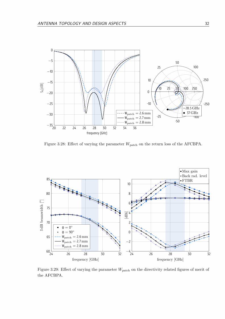
ANTENNA TOPOLOGY AND DESIGN ASPECTS 32
20 22 24 26 28 30 32 34 36−35
−30
−25
−20
−15
−10
−5
0
frequency [GHz]
S 11[dB
]
Wpatch = 2.6mmWpatch = 2.7mmWpatch = 2.8mm
10 25 50 100 2500
10
2550
100
250
-10
-25-50
-100
-25028.5GHz37GHz
Figure 3.28: Effect of varying the parameter Wpatch on the return loss of the AFCBPA.
24 26 28 30 3260
65
70
75
80
85
frequency [GHz]
3dB
beam
wid
th[o ]
φ = 0
φ = 90
Wpatch = 2.6mmWpatch = 2.7mmWpatch = 2.8mm
24 26 28 30 32−4
−2
0
2
4
6
8
10
frequency [GHz]
[dBi]
Max gainBack rad. levelFTBR
Figure 3.29: Effect of varying the parameter Wpatch on the directivity related figures of merit ofthe AFCBPA.
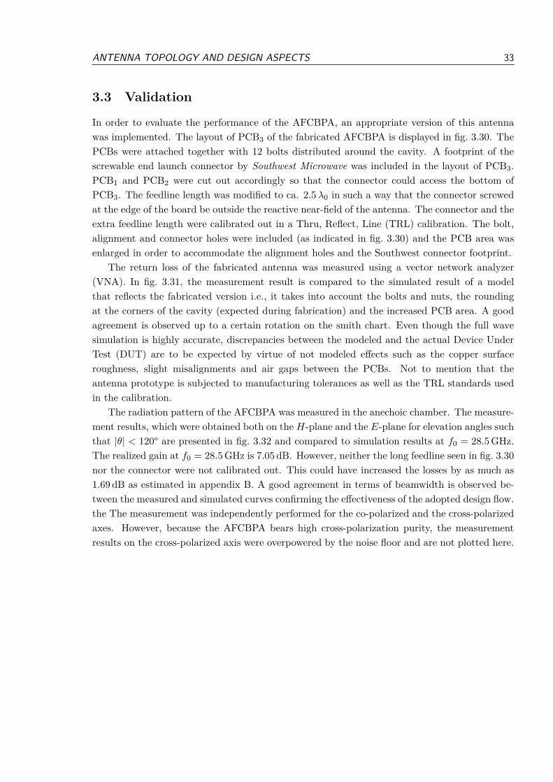
ANTENNA TOPOLOGY AND DESIGN ASPECTS 33
3.3 Validation
In order to evaluate the performance of the AFCBPA, an appropriate version of this antennawas implemented. The layout of PCB3 of the fabricated AFCBPA is displayed in fig. 3.30. ThePCBs were attached together with 12 bolts distributed around the cavity. A footprint of thescrewable end launch connector by Southwest Microwave was included in the layout of PCB3.PCB1 and PCB2 were cut out accordingly so that the connector could access the bottom ofPCB3. The feedline length was modified to ca. 2.5λ0 in such a way that the connector screwedat the edge of the board be outside the reactive near-field of the antenna. The connector and theextra feedline length were calibrated out in a Thru, Reflect, Line (TRL) calibration. The bolt,alignment and connector holes were included (as indicated in fig. 3.30) and the PCB area wasenlarged in order to accommodate the alignment holes and the Southwest connector footprint.
The return loss of the fabricated antenna was measured using a vector network analyzer(VNA). In fig. 3.31, the measurement result is compared to the simulated result of a modelthat reflects the fabricated version i.e., it takes into account the bolts and nuts, the roundingat the corners of the cavity (expected during fabrication) and the increased PCB area. A goodagreement is observed up to a certain rotation on the smith chart. Even though the full wavesimulation is highly accurate, discrepancies between the modeled and the actual Device UnderTest (DUT) are to be expected by virtue of not modeled effects such as the copper surfaceroughness, slight misalignments and air gaps between the PCBs. Not to mention that theantenna prototype is subjected to manufacturing tolerances as well as the TRL standards usedin the calibration.
The radiation pattern of the AFCBPA was measured in the anechoic chamber. The measure-ment results, which were obtained both on the H-plane and the E-plane for elevation angles suchthat |θ| < 120° are presented in fig. 3.32 and compared to simulation results at f0 = 28.5GHz.The realized gain at f0 = 28.5GHz is 7.05 dB. However, neither the long feedline seen in fig. 3.30nor the connector were not calibrated out. This could have increased the losses by as much as1.69 dB as estimated in appendix B. A good agreement in terms of beamwidth is observed be-tween the measured and simulated curves confirming the effectiveness of the adopted design flow.the The measurement was independently performed for the co-polarized and the cross-polarizedaxes. However, because the AFCBPA bears high cross-polarization purity, the measurementresults on the cross-polarized axis were overpowered by the noise floor and are not plotted here.
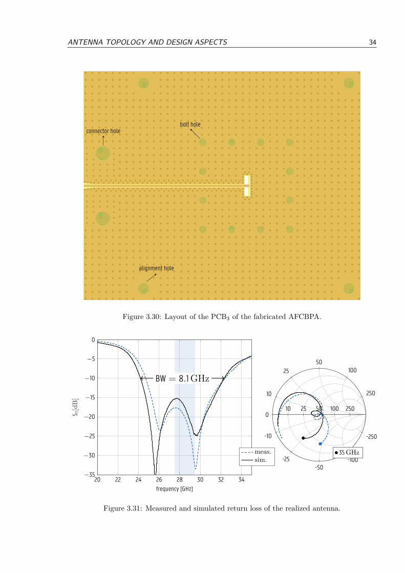
ANTENNA TOPOLOGY AND DESIGN ASPECTS 34
bolt holeconnector hole
alignment hole
Figure 3.30: Layout of the PCB3 of the fabricated AFCBPA.
20 22 24 26 28 30 32 34−35
−30
−25
−20
−15
−10
−5
0
BW = 8.1GHz
frequency [GHz]
S 11[dB
]
meas.sim.
10 25 50 100 2500
10
2550
100
250
-10
-25-50
-100
-250
35GHz
Figure 3.31: Measured and simulated return loss of the realized antenna.
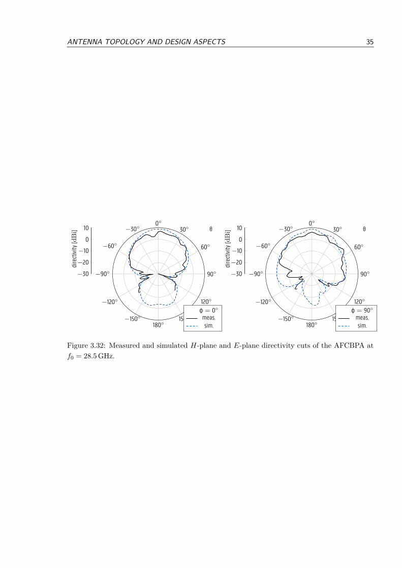
ANTENNA TOPOLOGY AND DESIGN ASPECTS 35
030
60
90
120
150180
−150
−120
−90
−60
−30
−30
−20
−100
10 θ
directivity[dBi]
φ = 0meas.sim.
030
60
90
120
150180
−150
−120
−90
−60
−30
−30
−20
−100
10 θdirectivity[dBi]
φ = 90meas.sim.
Figure 3.32: Measured and simulated H-plane and E-plane directivity cuts of the AFCBPA atf0 = 28.5GHz.
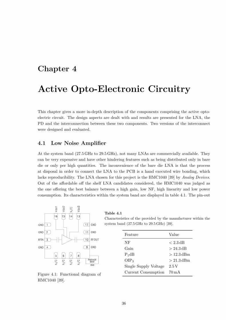
Chapter 4
Active Opto-Electronic Circuitry
This chapter gives a more in-depth description of the components comprising the active opto-electric circuit. The design aspects are dealt with and results are presented for the LNA, thePD and the interconnection between these two components. Two versions of the interconnectwere designed and evaluated.
4.1 Low Noise Amplifier
At the system band (27.5 GHz to 29.5 GHz), not many LNAs are commercially available. Theycan be very expensive and have other hindering features such as being distributed only in baredie or only per high quantities. The inconvenience of the bare die LNA is that the processat disposal in order to connect the LNA to the PCB is a hand executed wire bonding, whichlacks reproducibility. The LNA chosen for this project is the HMC1040 [39] by Analog Devices.Out of the affordable off the shelf LNA candidates considered, the HMC1040 was judged asthe one offering the best balance between a high gain, low NF, high linearity and low powerconsumption. Its characteristics within the system band are displayed in table 4.1. The pin-out
For price, delivery and to place orders: Hittite Microwave Corporation, 2 Elizabeth Drive, Chelmsford, MA 01824Phone: 978-250-3343 Fax: 978-250-3373 Order On-line at www.hittite.com
Application Support: Phone: 978-250-3343 or [email protected]
Am
pli
fie
rs
- l
ow
No
ise
- s
mT
1
HMC1040LP3CEv00.0112
GaAs pHEMT MMIC LOW NOISEAMPLIFIER, 24 - 43.5 GHz
General Description
Features
Functional Diagram
low Noise figure: 2.2 dB
High Gain: 23 dB
p1dB output power: +12 dBm
single supply: +2.5V @ 70 mA
output ip3: +22 dBm
50 ohm matched input/output
16 lead 3x3 mm smT package: 16mm²
Electrical Specifications, TA = +25° C, Vdd1 = Vdd2 = Vdd3 = +2.5V, Idd = 70 mA
Typical ApplicationsThis HmC1040lp3Be is ideal for:
• Point-to-Point Radios
• Test Instrumentation
• SatCom Transponders & VSAT
• Industrial Sensors
• EW & ECM Subsystems
The HMC1040LP3CE is a self-biased GaAs MMIC low Noise Amplifier housed in a leadless 3x3 mm plastic surface mount package. The amplifier operates between 24 and 43.5 GHz, delivering 23 dB of small signal gain, 2.2 dB noise figure, and output IP3 of +22 dBm, while requiring only 70 mA from a +2.5 V supply. The P1dB output power of +12 dBm enables the LNA to function as a LO driver for many of Hittite’s balanced, I/Q and image reject mixers. The HmC1040lp3Ce fe- atures I/Os that are DC blocked and internally mat-ched to 50 Ohms, and is ideal for high capacity microwave radios and VsAT applications.
parameter min. Typ. max. min. Typ. max. min. Typ. max. Units
Frequency Range 24 - 27.5 27.5 - 33.5 33.5 - 43.5 GHz
Gain [1] 22 25 20 23 17 20 dB
Gain Variation over Temperature 0.022 0.021 0.021 dB /°C
Noise figure [1] 2.7 3.2 2.2 2.7 2.7 3.2 dB
input return loss 11 12 10 dB
output return loss 16 13 10 dB
output power for 1 dB Compression 12 12 12 dBm
saturated output power (psat) 14 14 14 dBm
output Third order intercept (ip3) 22 22 24 dBm
supply Current (idd) (Vdd = 2.5V)
70 85 70 85 70 85 mA
[1] Board loss subtracted out.
Information furnished by Analog Devices is believed to be accurate and reliable. However, no responsibility is assumed by Analog Devices for its use, nor for any infringements of patents or other rights of third parties that may result from its use. Specifications subject to change without notice. No license is granted by implication or otherwise under any patent or patent rights of Analog Devices. Trademarks and registered trademarks are the property of their respective owners.
For price, delivery, and to place orders: Analog Devices, Inc., One Technology Way, P.O. Box 9106, Norwood, MA 02062-9106 Phone: 781-329-4700 • Order online at www.analog.com Application Support: Phone: 1-800-ANALOG-D
Figure 4.1: Functional diagram ofHMC1040 [39].
Table 4.1Characteristics of the provided by the manufacturer within thesystem band (27.5GHz to 29.5 GHz) [39].
Feature Value
NF < 2.3 dB
Gain > 24.3 dB
P1dB > 12.3 dBm
OIP3 > 21.3 dBm
Single Supply Voltage 2.5 VCurrent Consumption 70 mA
36
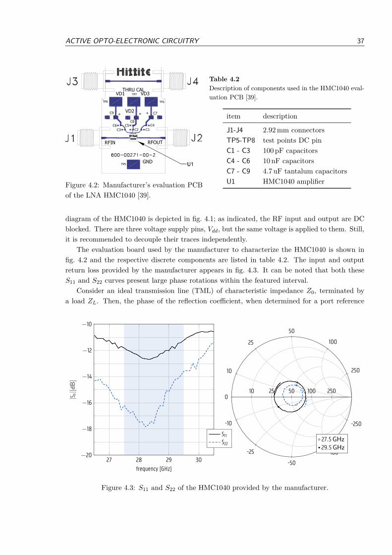
ACTIVE OPTO-ELECTRONIC CIRCUITRY 37
For price, delivery and to place orders: Hittite Microwave Corporation, 2 Elizabeth Drive, Chelmsford, MA 01824Phone: 978-250-3343 Fax: 978-250-3373 Order On-line at www.hittite.com
Application Support: Phone: 978-250-3343 or [email protected]
Am
pli
fie
rs
- l
ow
No
ise
- s
mT
6
HMC1040LP3CEv00.0112
GaAs pHEMT MMIC LOW NOISEAMPLIFIER, 24 - 43.5 GHz
item Description
J1-J4 2.92 mm Connectors
Tp5-Tp8 Test points DC pin
C1 - C3 100 pF Capacitor, 0402 Pkg.
C4 - C6 10 nF Capacitor, 0402 Pkg.
C7 - C9 4.7 µF Capacitor, Tantalum
U1 HmC1040lp3Ce Amplifier
pCB [2] 600-00271-00-2 evaluation pCB
[1] Reference this number when ordering complete evaluation PCB
[2] Circuit Board material: rogers 4350 or Arlon 25fr
The circuit board used in this application should use RF circuit design techniques. Signal lines should have 50 ohm impedance while the pack-age ground leads and exposed paddle should be connected directly to the ground plane similar to that shown. A sufficient number of via holes should be used to connect the top and bottom ground planes. The evaluation board should be mounted to an appropriate heat sink. The evaluation circuit board shown is available from Hittite upon request.
List of Material for Evaluation PCB EVAL01-HMC1040LP3CE [1]
Evaluation PCB
Information furnished by Analog Devices is believed to be accurate and reliable. However, no responsibility is assumed by Analog Devices for its use, nor for any infringements of patents or other rights of third parties that may result from its use. Specifications subject to change without notice. No license is granted by implication or otherwise under any patent or patent rights of Analog Devices. Trademarks and registered trademarks are the property of their respective owners.
For price, delivery, and to place orders: Analog Devices, Inc., One Technology Way, P.O. Box 9106, Norwood, MA 02062-9106 Phone: 781-329-4700 • Order online at www.analog.com Application Support: Phone: 1-800-ANALOG-D
Figure 4.2: Manufacturer’s evaluation PCBof the LNA HMC1040 [39].
Table 4.2Description of components used in the HMC1040 eval-uation PCB [39].
item description
J1-J4 2.92mm connectorsTP5-TP8 test points DC pinC1 - C3 100 pF capacitorsC4 - C6 10 nF capacitorsC7 - C9 4.7 uF tantalum capacitorsU1 HMC1040 amplifier
diagram of the HMC1040 is depicted in fig. 4.1; as indicated, the RF input and output are DCblocked. There are three voltage supply pins, Vdd, but the same voltage is applied to them. Still,it is recommended to decouple their traces independently.
The evaluation board used by the manufacturer to characterize the HMC1040 is shown infig. 4.2 and the respective discrete components are listed in table 4.2. The input and outputreturn loss provided by the manufacturer appears in fig. 4.3. It can be noted that both theseS11 and S22 curves present large phase rotations within the featured interval.
Consider an ideal transmission line (TML) of characteristic impedance Z0, terminated bya load ZL. Then, the phase of the reflection coefficient, when determined for a port reference
27 28 29 30−20
−18
−16
−14
−12
−10
frequency [GHz]
|S ii|[dB
]
S11S22
10 25 50 100 2500
10
25
50
100
250
-10
-25
-50
-100
-250
27.5GHz29.5GHz
Figure 4.3: S11 and S22 of the HMC1040 provided by the manufacturer.
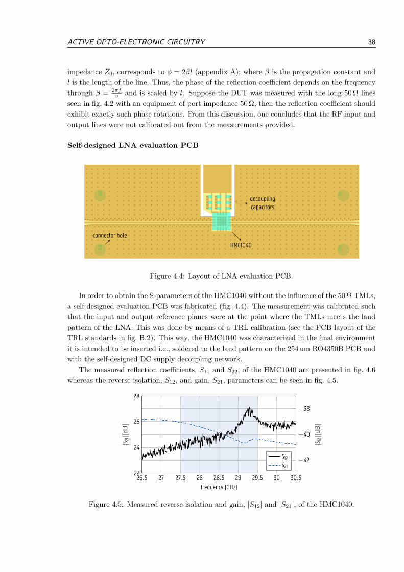
ACTIVE OPTO-ELECTRONIC CIRCUITRY 38
impedance Z0, corresponds to ϕ = 2βl (appendix A); where β is the propagation constant andl is the length of the line. Thus, the phase of the reflection coefficient depends on the frequencythrough β = 2πf
v and is scaled by l. Suppose the DUT was measured with the long 50Ω linesseen in fig. 4.2 with an equipment of port impedance 50 Ω, then the reflection coefficient shouldexhibit exactly such phase rotations. From this discussion, one concludes that the RF input andoutput lines were not calibrated out from the measurements provided.
Self-designed LNA evaluation PCB
connector hole
HMC1040
decouplingcapacitors
Figure 4.4: Layout of LNA evaluation PCB.
In order to obtain the S-parameters of the HMC1040 without the influence of the 50 Ω TMLs,a self-designed evaluation PCB was fabricated (fig. 4.4). The measurement was calibrated suchthat the input and output reference planes were at the point where the TMLs meets the landpattern of the LNA. This was done by means of a TRL calibration (see the PCB layout of theTRL standards in fig. B.2). This way, the HMC1040 was characterized in the final environmentit is intended to be inserted i.e., soldered to the land pattern on the 254 um RO4350B PCB andwith the self-designed DC supply decoupling network.
The measured reflection coefficients, S11 and S22, of the HMC1040 are presented in fig. 4.6whereas the reverse isolation, S12, and gain, S21, parameters can be seen in fig. 4.5.
26.5 27 27.5 28 28.5 29 29.5 30 30.522
24
26
28
−42
−40
−38
frequency [GHz]
|S 21|[dB
]
|S 12|[dB
]
S12S21
Figure 4.5: Measured reverse isolation and gain, |S12| and |S21|, of the HMC1040.
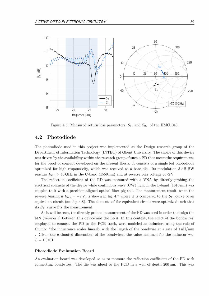
ACTIVE OPTO-ELECTRONIC CIRCUITRY 39
27 28 29 30−15
−14
−13
−12
−11
−10
frequency [GHz]
|S ii|[dB
]
S11S22
10 25 50 100 2500
10
25
50
100
250
-10
-25
-50
-100
-250S11
S22
30.5GHz
Figure 4.6: Measured return loss parameters, S11 and S22, of the HMC1040.
4.2 Photodiode
The photodiode used in this project was implemented at the Design research group of theDepartment of Information Technology (INTEC) of Ghent University. The choice of this devicewas driven by the availability within the research group of such a PD that meets the requirementsfor the proof of concept developed on the present thesis. It consists of a single fed photodiodeoptimized for high responsivity, which was received as a bare die. Its modulation 3-dB-BWreaches f3dB > 40GHz in the C-band (1550 nm) and at reverse bias voltage of -2 V
The reflection coefficient of the PD was measured with a VNA by directly probing theelectrical contacts of the device while continuous wave (CW) light in the L-band (1610 nm) wascoupled to it with a precision aligned optical fiber pig tail. The measurement result, when thereverse biasing is Vrev = −2V, is shown in fig. 4.7 where it is compared to the S11 curve of anequivalent circuit (see fig. 4.8). The elements of the equivalent circuit were optimized such thatits S11 curve fits the measurement.
As it will be seen, the directly probed measurement of the PD was used in order to design theMN (version 1) between this device and the LNA. In this context, the effect of the bondwires,employed to connect the PD to the PCB track, were modeled as inductors using the rule ofthumb: “the inductance scales linearly with the length of the bondwire at a rate of 1 nH/mm
. Given the estimated dimensions of the bondwires, the value assumed for the inductor wasL = 1.3 nH.
Photodiode Evalutation Board
An evaluation board was developed so as to measure the reflection coefficient of the PD withconnecting bondwires. The die was glued to the PCB in a well of depth 200 um. This was
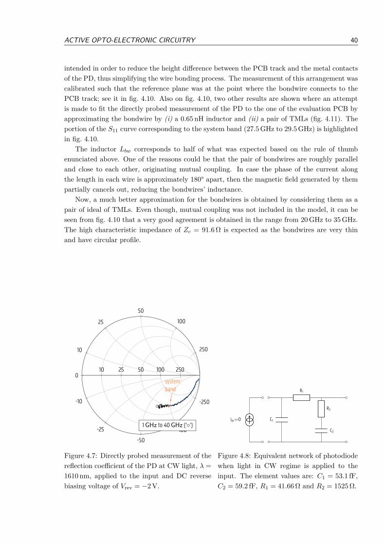
ACTIVE OPTO-ELECTRONIC CIRCUITRY 40
intended in order to reduce the height difference between the PCB track and the metal contactsof the PD, thus simplifying the wire bonding process. The measurement of this arrangement wascalibrated such that the reference plane was at the point where the bondwire connects to thePCB track; see it in fig. 4.10. Also on fig. 4.10, two other results are shown where an attemptis made to fit the directly probed measurement of the PD to the one of the evaluation PCB byapproximating the bondwire by (i) a 0.65 nH inductor and (ii) a pair of TMLs (fig. 4.11). Theportion of the S11 curve corresponding to the system band (27.5GHz to 29.5 GHz) is highlightedin fig. 4.10.
The inductor Lbw corresponds to half of what was expected based on the rule of thumbenunciated above. One of the reasons could be that the pair of bondwires are roughly paralleland close to each other, originating mutual coupling. In case the phase of the current alongthe length in each wire is approximately 180° apart, then the magnetic field generated by thempartially cancels out, reducing the bondwires’ inductance.
Now, a much better approximation for the bondwires is obtained by considering them as apair of ideal of TMLs. Even though, mutual coupling was not included in the model, it can beseen from fig. 4.10 that a very good agreement is obtained in the range from 20 GHz to 35 GHz.The high characteristic impedance of Zc = 91.6Ω is expected as the bondwires are very thinand have circular profile.
10 25 50 100 2500
10
25
50
100
250
-10
-25
-50
-100
-250
systemband
1GHz to 40GHz (‘’)
Figure 4.7: Directly probed measurement of thereflection coefficient of the PD at CW light, λ =
1610 nm, applied to the input and DC reversebiasing voltage of Vrev = −2V.
iac=0 C1
R1
R2
C2
Figure 4.8: Equivalent network of photodiodewhen light in CW regime is applied to theinput. The element values are: C1 = 53.1 fF,C2 = 59.2 fF, R1 = 41.66Ω and R2 = 1525Ω.
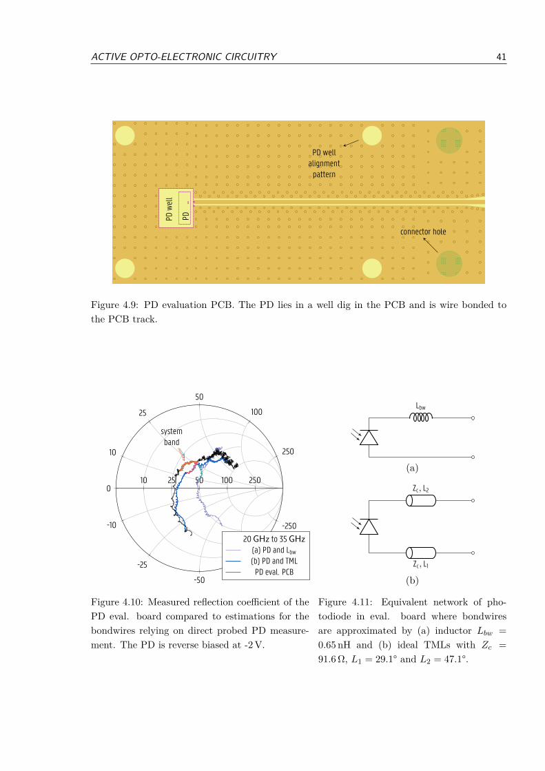
ACTIVE OPTO-ELECTRONIC CIRCUITRY 41
connector hole
PD wellalignmentpattern
PDPDwell
Figure 4.9: PD evaluation PCB. The PD lies in a well dig in the PCB and is wire bonded tothe PCB track.
10 25 50 100 2500
10
25
50
100
250
-10
-25
-50
-100
-25020GHz to 35GHz(a) PD and Lbw(b) PD and TMLPD eval. PCB
systemband
Figure 4.10: Measured reflection coefficient of thePD eval. board compared to estimations for thebondwires relying on direct probed PD measure-ment. The PD is reverse biased at -2V.
Lbw
(a)
Zc, L1
Zc, L2
(b)
Figure 4.11: Equivalent network of pho-todiode in eval. board where bondwiresare approximated by (a) inductor Lbw =
0.65 nH and (b) ideal TMLs with Zc =
91.6Ω, L1 = 29.1° and L2 = 47.1°.
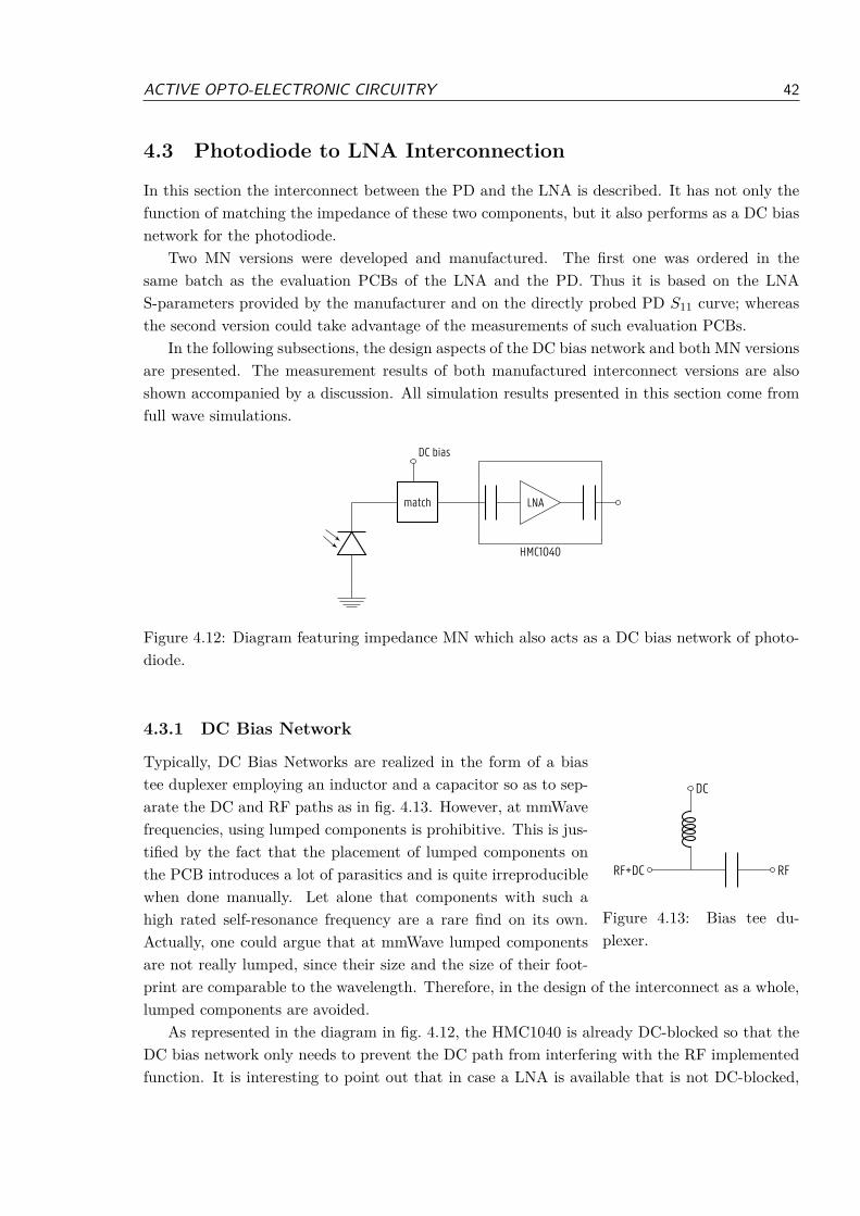
ACTIVE OPTO-ELECTRONIC CIRCUITRY 42
4.3 Photodiode to LNA Interconnection
In this section the interconnect between the PD and the LNA is described. It has not only thefunction of matching the impedance of these two components, but it also performs as a DC biasnetwork for the photodiode.
Two MN versions were developed and manufactured. The first one was ordered in thesame batch as the evaluation PCBs of the LNA and the PD. Thus it is based on the LNAS-parameters provided by the manufacturer and on the directly probed PD S11 curve; whereasthe second version could take advantage of the measurements of such evaluation PCBs.
In the following subsections, the design aspects of the DC bias network and both MN versionsare presented. The measurement results of both manufactured interconnect versions are alsoshown accompanied by a discussion. All simulation results presented in this section come fromfull wave simulations.
match LNA
HMC1040
DC bias
Figure 4.12: Diagram featuring impedance MN which also acts as a DC bias network of photo-diode.
4.3.1 DC Bias Network
RF+DC
DC
RF
Figure 4.13: Bias tee du-plexer.
Typically, DC Bias Networks are realized in the form of a biastee duplexer employing an inductor and a capacitor so as to sep-arate the DC and RF paths as in fig. 4.13. However, at mmWavefrequencies, using lumped components is prohibitive. This is jus-tified by the fact that the placement of lumped components onthe PCB introduces a lot of parasitics and is quite irreproduciblewhen done manually. Let alone that components with such ahigh rated self-resonance frequency are a rare find on its own.Actually, one could argue that at mmWave lumped componentsare not really lumped, since their size and the size of their foot-print are comparable to the wavelength. Therefore, in the design of the interconnect as a whole,lumped components are avoided.
As represented in the diagram in fig. 4.12, the HMC1040 is already DC-blocked so that theDC bias network only needs to prevent the DC path from interfering with the RF implementedfunction. It is interesting to point out that in case a LNA is available that is not DC-blocked,
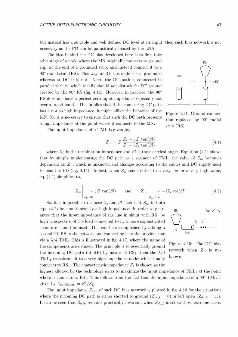
ACTIVE OPTO-ELECTRONIC CIRCUITRY 43
but instead has a suitable and well defined DC level at its input, then such bias network is notnecessary as the PD can be parasitically biased by the LNA.
DC
RS1
=⇒
Figure 4.14: Ground connec-tion replaced by 90° radialstub (RS).
The idea behind the DC bias developed here is to first takeadvantage of a node where the MN originally connects to grounde.g., at the end of a grounded stub, and instead connect it to a90° radial stub (RS). This way, at RF this node is still groundedwhereas at DC it is not. Next, the DC path is connected inparallel with it, which ideally should not disturb the RF groundcreated by the 90° RS (fig. 4.14). However, in practice, the 90°RS does not have a perfect zero input impedance (specially notover a broad band). This implies that if the connecting DC pathhas a not so high impedance, it might affect the behavior of theMN. So, it is necessary to ensure that such the DC path presentsa high impedance at the point where it connects to the MN.
The input impedance of a TML is given by,
Zin = ZcZL + jZc tan(βl)
Zc + jZL tan(βl)(4.1)
where ZL is the termination impedance and βl is the electrical angle. Equation (4.1) showsthat by simply implementing the DC path as a segment of TML, the value of Zin becomesdependent on ZL, which is unknown and changes according to the cables and DC supply usedto bias the PD (fig. 4.15). Indeed, when ZL tends either to a very low or a very high value,eq. (4.1) simplifies to,
Zin
∣∣∣∣∣ZL→0
= jZc tan(βl) and Zin
∣∣∣∣∣ZL→∞
= −jZc cot(βl) (4.2)
RS1
TML
Vdc
ZL =?
Figure 4.15: The DC biasnetwork when ZL is un-known.
So, it is impossible to choose Zc and βl such that Zin in botheqs. (4.2) be simultaneously a high impedance. In order to guar-antee that the input impedance of the line in shunt with RS1 behigh irrespective of the load connected to it, a more sophisticatedstructure should be used. This can be accomplished by adding asecond 90° RS to the network and connecting it to the previous onevia a λ/4 TML. This is illustrated in fig. 4.17, where the name ofthe components are defined. The principle is to essentially groundthe incoming DC path (at RF) by means of RS2, then the λ/4
TML1 transforms it to a very high impedance node; which finallyconnects to RS1. The characteristic impedance Z1 is chosen as thehighest allowed by the technology so as to maximize the input impedance of TML1 at the pointwhere it connects to RS1. This follows from the fact that the input impedance of a 90° TML isgiven by Zin|βl=90 = Z2
c /ZL.The input impedance Zb,in of such DC bias network is plotted in fig. 4.16 for the situations
where the incoming DC path is either shorted to ground (Zdc,L = 0) or left open (Zdc,L = ∞).It can be seen that Zb,in remains practically invariant when Zdc,L is set to those extreme cases.
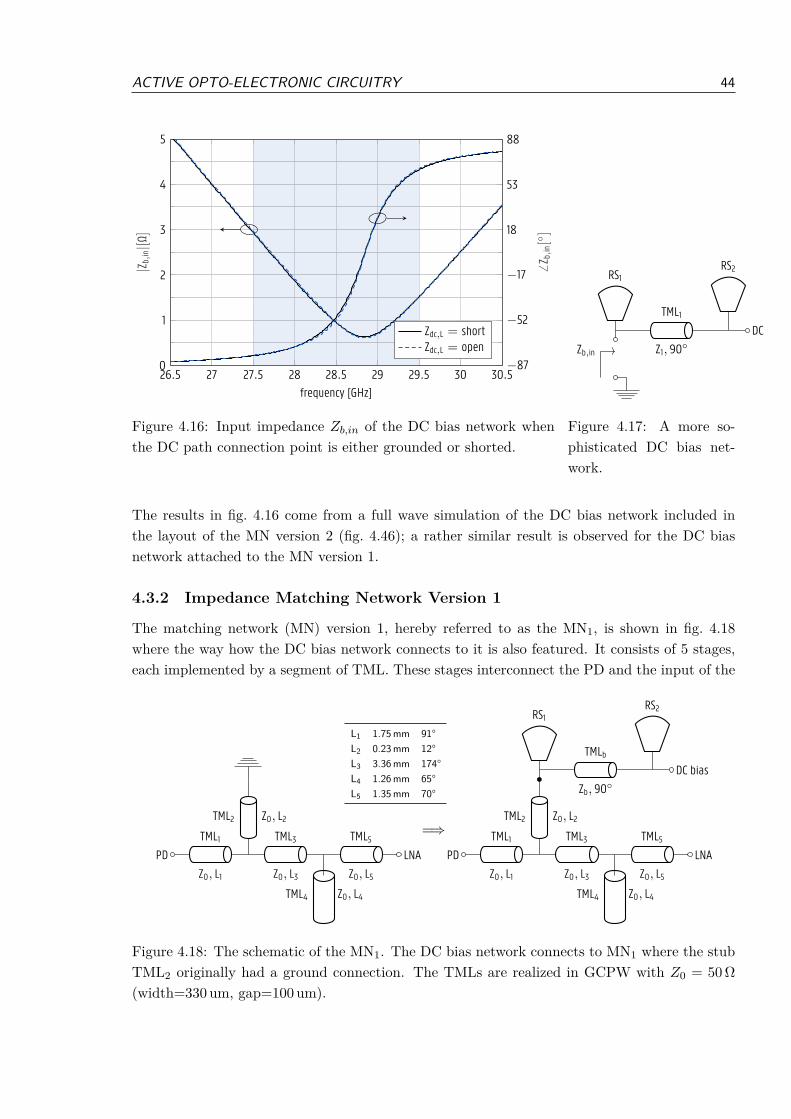
ACTIVE OPTO-ELECTRONIC CIRCUITRY 44
26.5 27 27.5 28 28.5 29 29.5 30 30.50
1
2
3
4
5
−87
−52
−17
18
53
88
frequency [GHz]
|Z b,in|[Ω
]
Z b,in
[]
Zdc,L = shortZdc,L = open
Figure 4.16: Input impedance Zb,in of the DC bias network whenthe DC path connection point is either grounded or shorted.
RS1
Zb,in
TML1
Z1, 90
RS2
DC
Figure 4.17: A more so-phisticated DC bias net-work.
The results in fig. 4.16 come from a full wave simulation of the DC bias network included inthe layout of the MN version 2 (fig. 4.46); a rather similar result is observed for the DC biasnetwork attached to the MN version 1.
4.3.2 Impedance Matching Network Version 1
The matching network (MN) version 1, hereby referred to as the MN1, is shown in fig. 4.18where the way how the DC bias network connects to it is also featured. It consists of 5 stages,each implemented by a segment of TML. These stages interconnect the PD and the input of the
L1 1.75 mm 91°L2 0.23 mm 12°L3 3.36 mm 174°L4 1.26 mm 65°L5 1.35 mm 70°
PDTML1
Z0, L1
TML2 Z0, L2TML3
Z0, L3
TML5
Z0, L5
LNA
Z0, L4TML4
=⇒
PDTML1
Z0, L1
TML2 Z0, L2TML3
Z0, L3
TML5
Z0, L5
LNA
Z0, L4TML4
RS1
TMLb
Zb, 90
RS2
DC bias
Figure 4.18: The schematic of the MN1. The DC bias network connects to MN1 where the stubTML2 originally had a ground connection. The TMLs are realized in GCPW with Z0 = 50Ω
(width=330 um, gap=100 um).
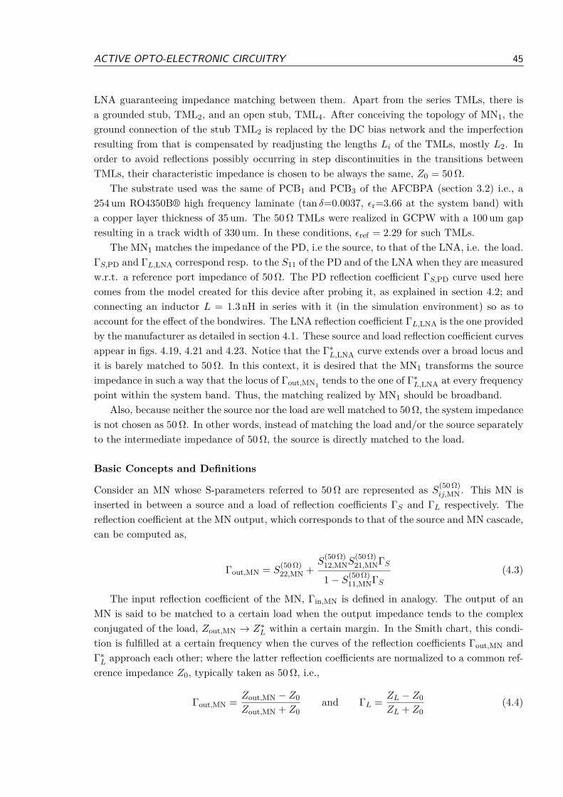
ACTIVE OPTO-ELECTRONIC CIRCUITRY 45
LNA guaranteeing impedance matching between them. Apart from the series TMLs, there isa grounded stub, TML2, and an open stub, TML4. After conceiving the topology of MN1, theground connection of the stub TML2 is replaced by the DC bias network and the imperfectionresulting from that is compensated by readjusting the lengths Li of the TMLs, mostly L2. Inorder to avoid reflections possibly occurring in step discontinuities in the transitions betweenTMLs, their characteristic impedance is chosen to be always the same, Z0 = 50Ω.
The substrate used was the same of PCB1 and PCB3 of the AFCBPA (section 3.2) i.e., a254 um RO4350B® high frequency laminate (tan δ=0.0037, ϵr=3.66 at the system band) witha copper layer thickness of 35 um. The 50 Ω TMLs were realized in GCPW with a 100 um gapresulting in a track width of 330 um. In these conditions, ϵref = 2.29 for such TMLs.
The MN1 matches the impedance of the PD, i.e the source, to that of the LNA, i.e. the load.ΓS,PD and ΓL,LNA correspond resp. to the S11 of the PD and of the LNA when they are measuredw.r.t. a reference port impedance of 50 Ω. The PD reflection coefficient ΓS,PD curve used herecomes from the model created for this device after probing it, as explained in section 4.2; andconnecting an inductor L = 1.3 nH in series with it (in the simulation environment) so as toaccount for the effect of the bondwires. The LNA reflection coefficient ΓL,LNA is the one providedby the manufacturer as detailed in section 4.1. These source and load reflection coefficient curvesappear in figs. 4.19, 4.21 and 4.23. Notice that the Γ∗
L,LNA curve extends over a broad locus andit is barely matched to 50 Ω. In this context, it is desired that the MN1 transforms the sourceimpedance in such a way that the locus of Γout,MN1
tends to the one of Γ∗L,LNA at every frequency
point within the system band. Thus, the matching realized by MN1 should be broadband.Also, because neither the source nor the load are well matched to 50 Ω, the system impedance
is not chosen as 50 Ω. In other words, instead of matching the load and/or the source separatelyto the intermediate impedance of 50 Ω, the source is directly matched to the load.
Basic Concepts and Definitions
Consider an MN whose S-parameters referred to 50 Ω are represented as S(50Ω)ij,MN . This MN is
inserted in between a source and a load of reflection coefficients ΓS and ΓL respectively. Thereflection coefficient at the MN output, which corresponds to that of the source and MN cascade,can be computed as,
Γout,MN = S(50Ω)22,MN +
S(50Ω)12,MNS
(50Ω)21,MNΓS
1− S(50Ω)11,MNΓS
(4.3)
The input reflection coefficient of the MN, Γin,MN is defined in analogy. The output of anMN is said to be matched to a certain load when the output impedance tends to the complexconjugated of the load, Zout,MN → Z∗
L within a certain margin. In the Smith chart, this condi-tion is fulfilled at a certain frequency when the curves of the reflection coefficients Γout,MN andΓ∗L approach each other; where the latter reflection coefficients are normalized to a common ref-
erence impedance Z0, typically taken as 50Ω, i.e.,
Γout,MN =Zout,MN − Z0
Zout,MN + Z0and ΓL =
ZL − Z0
ZL + Z0(4.4)
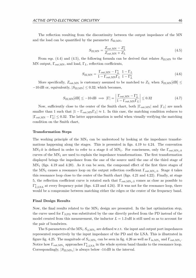
ACTIVE OPTO-ELECTRONIC CIRCUITRY 46
The reflection resulting from the discontinuity between the output impedance of the MNand the load can be quantified by the parameter S22,MN,
S22,MN =Zout,MN − Z∗
L
Zout,MN + ZL(4.5)
From eqs. (4.4) and (4.5), the following formula can be derived that relates S22,MN to theMN output, Γout,MN, and load, ΓL, reflection coefficients,
S22,MN =Γout,MN − Γ∗
L
1− Γout,MNΓL
1− ΓL
1− Γ∗L
(4.6)
More specifically, Zout,MN is customary assumed to be matched to ZL when S22,MN[dB] ≤−10 dB or, equivalently, |S22,MN| ≤ 0.32; which becomes,
S22,MN[dB] ≤ −10 dB =⇒ |Γ| =∣∣∣∣ Γout,MN − Γ∗
L
1− Γout,MNΓL
∣∣∣∣ ≤ 0.32 (4.7)
Now, sufficiently close to the center of the Smith chart, both |Γout,MN| and |ΓL| are muchsmaller than 1 such that |1 − Γout,MNΓL| ≈ 1. In this case, the matching condition reduces to|Γout,MN − Γ∗
L| ≤ 0.32. The latter approximation is useful when visually verifying the matchingcondition on the Smith chart,
Transformation Steps
The working principle of the MN1 can be understood by looking at the impedance transfor-mations happening along the stages. This is presented in figs. 4.19 to 4.24. The conventionMN1:k is defined in order to refer to a stage k of MN1. For conciseness, only the Γout,MN1:k
curves of the MN1 are used to explain the impedance transformations. The first transformationdisplayed brings the impedance from the one of the source until the one of the third stage ofMN1 (figs. 4.19 and 4.20). As it can be seen, the compound effect of the first three stages ofthe MN1 causes a resonance loop on the output reflection coefficient Γout,MN1:3. Stage 4 takesthis resonance loop close to the center of the Smith chart (figs. 4.21 and 4.22). Finally, at stage5, the reflection coefficient curve is rotated such that Γout,MN1:3 comes as close as possible toΓ∗L,LNA at every frequency point (figs. 4.23 and 4.24). If it was not for the resonance loop, there
would be a compromise between matching either the edges or the center of the frequency band.
Final Design Results
Now, the final results related to the MN1 design are presented. In the last optimization step,the curve used for ΓS,PD was substituted by the one directly probed from the PD instead of themodel created from this measurement, the inductor L = 1.3 uH is still used so as to account forthe pair of bondwires.
The S-parameters of the MN1 Sij,MN1 are defined w.r.t. the input and output port impedancesrepresented respectively by the input impedance of the PD and the LNA. This is illustrated infigure fig. 4.25. The magnitude of Sii,MN1 can be seen in fig. 4.26 as well as Γin,MN1
and Γout,MN1.
Notice how Γout,MN1approaches Γ∗
L,LNA in the whole system band thanks to the resonance loop.Correspondingly, |S22,MN1 | is always below -14 dB in the interval.

ACTIVE OPTO-ELECTRONIC CIRCUITRY 47
10 25 50 100 2500
10
25
50
100
250
-10
-25
-50
-100
-250
27.5GHz to 29.5GHz (‘’)
Γ∗L,LNA
ΓS,PDΓout,MN1:3
Figure 4.19: MN1 transformation step fromsource to stage 3. The featured curves are: S22
of the MN1 stage 3; S11 of the PD (source) andcomplex conjugated S11 of the LNA (load).
TML1
Z0, L1
TML2 Z0, L2TML3
Z0, L350 Ω
DC bias
Γout,MN1:3
Figure 4.20: Stage 3 of MN1 featuringΓout,MN1:3 definition
10 25 50 100 2500
10
25
50
100
250
-10
-25
-50
-100
-250
27.5GHz to 29.5GHz (‘’)
Γ∗L,LNA
ΓS,PDΓout,MN1:3
Γout,MN1:4
Figure 4.21: MN1 transformation step fromstage 3 to stage 4. The featured curves are:S22 of the MN1 stages 3 and 4; S11 of the PD(source) and complex conjugated S11 of the LNA(load).
TML1
Z0, L1
TML2 Z0, L2TML3
Z0, L3Z0, L4TML4 50 Ω
DC bias
Γout,MN1:4
Figure 4.22: Stage 4 of MN1 featuringΓout,MN1:4 definition
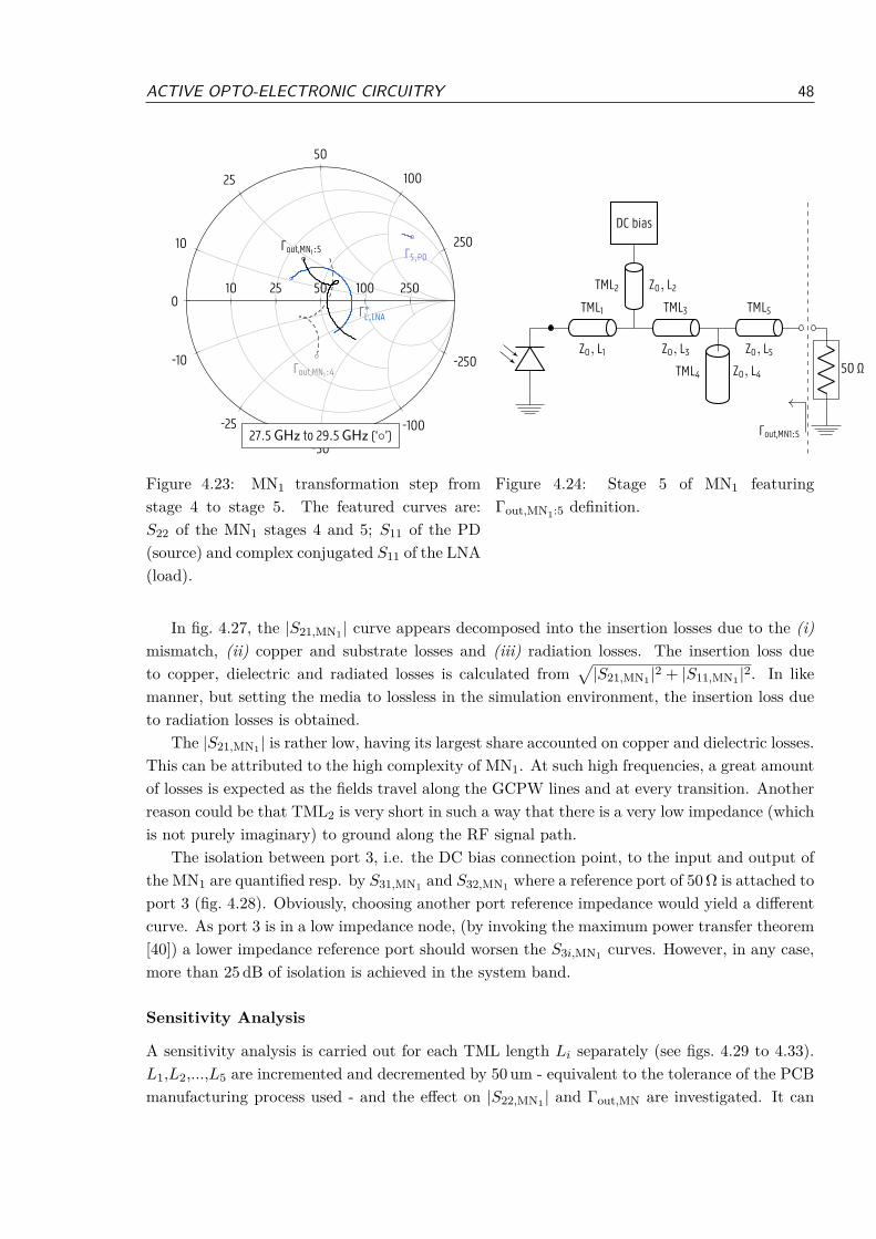
ACTIVE OPTO-ELECTRONIC CIRCUITRY 48
10 25 50 100 2500
10
25
50
100
250
-10
-25
-50
-100
-250
27.5GHz to 29.5GHz (‘’)
Γ∗L,LNA
ΓS,PD
Γout,MN1:4
Γout,MN1:5
Figure 4.23: MN1 transformation step fromstage 4 to stage 5. The featured curves are:S22 of the MN1 stages 4 and 5; S11 of the PD(source) and complex conjugated S11 of the LNA(load).
TML1
Z0, L1
TML2 Z0, L2TML3
Z0, L3
TML5
Z0, L5Z0, L4TML4 50 Ω
DC bias
Γout,MN1:5
Figure 4.24: Stage 5 of MN1 featuringΓout,MN1:5 definition.
In fig. 4.27, the |S21,MN1 | curve appears decomposed into the insertion losses due to the (i)mismatch, (ii) copper and substrate losses and (iii) radiation losses. The insertion loss dueto copper, dielectric and radiated losses is calculated from
√|S21,MN1 |2 + |S11,MN1 |2. In like
manner, but setting the media to lossless in the simulation environment, the insertion loss dueto radiation losses is obtained.
The |S21,MN1 | is rather low, having its largest share accounted on copper and dielectric losses.This can be attributed to the high complexity of MN1. At such high frequencies, a great amountof losses is expected as the fields travel along the GCPW lines and at every transition. Anotherreason could be that TML2 is very short in such a way that there is a very low impedance (whichis not purely imaginary) to ground along the RF signal path.
The isolation between port 3, i.e. the DC bias connection point, to the input and output ofthe MN1 are quantified resp. by S31,MN1 and S32,MN1 where a reference port of 50Ω is attached toport 3 (fig. 4.28). Obviously, choosing another port reference impedance would yield a differentcurve. As port 3 is in a low impedance node, (by invoking the maximum power transfer theorem[40]) a lower impedance reference port should worsen the S3i,MN1 curves. However, in any case,more than 25 dB of isolation is achieved in the system band.
Sensitivity Analysis
A sensitivity analysis is carried out for each TML length Li separately (see figs. 4.29 to 4.33).L1,L2,...,L5 are incremented and decremented by 50 um - equivalent to the tolerance of the PCBmanufacturing process used - and the effect on |S22,MN1 | and Γout,MN are investigated. It can
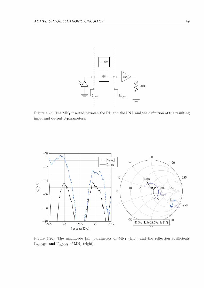
ACTIVE OPTO-ELECTRONIC CIRCUITRY 49
MN1 LNA
50 Ω
DC bias
S11,MN1 S22,MN1
Figure 4.25: The MN1 inserted between the PD and the LNA and the definition of the resultinginput and output S-parameters.
27.5 28 28.5 29 29.5−20
−18
−16
−14
−12
−10
frequency [GHz]
|S ii|[dB
]
|S11,MN1 ||S22,MN1 |
10 25 50 100 2500
10
25
50
100
250
-10
-25
-50
-100
-250
27.5GHz to 29.5GHz (‘’)
Γ∗L,LNA
Γin,MN1
Γ∗S,PD
Γout,MN1
Figure 4.26: The magnitude |Sii| parameters of MN1 (left); and the reflection coefficientsΓout,MN1
and Γin,MN1 of MN1 (right).
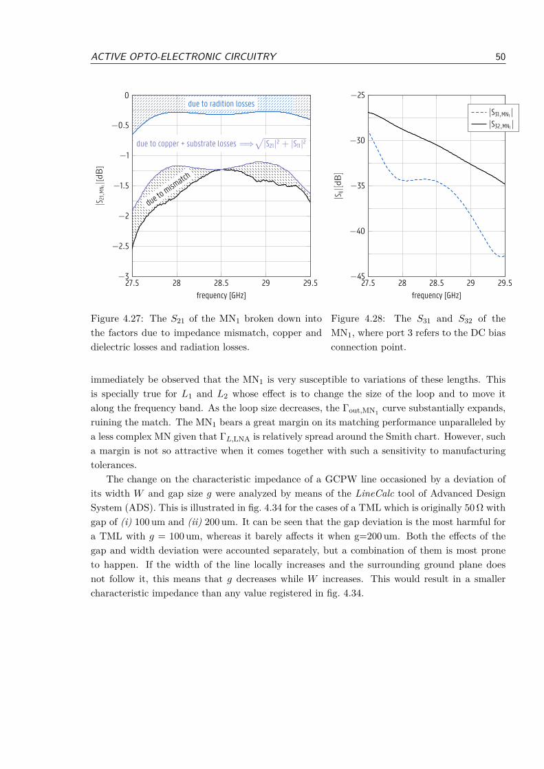
ACTIVE OPTO-ELECTRONIC CIRCUITRY 50
27.5 28 28.5 29 29.5−3
−2.5
−2
−1.5
−1
−0.5
0
dueto m
ismatch
due to copper + substrate losses =⇒√
|S21|2 + |S11|2
due to radition losses
frequency [GHz]
|S 21,MN 1|[d
B]
Figure 4.27: The S21 of the MN1 broken down intothe factors due to impedance mismatch, copper anddielectric losses and radiation losses.
27.5 28 28.5 29 29.5−45
−40
−35
−30
−25
frequency [GHz]
|S ij|[dB
]
|S31,MN1 ||S32,MN1 |
Figure 4.28: The S31 and S32 of theMN1, where port 3 refers to the DC biasconnection point.
immediately be observed that the MN1 is very susceptible to variations of these lengths. Thisis specially true for L1 and L2 whose effect is to change the size of the loop and to move italong the frequency band. As the loop size decreases, the Γout,MN1
curve substantially expands,ruining the match. The MN1 bears a great margin on its matching performance unparalleled bya less complex MN given that ΓL,LNA is relatively spread around the Smith chart. However, sucha margin is not so attractive when it comes together with such a sensitivity to manufacturingtolerances.
The change on the characteristic impedance of a GCPW line occasioned by a deviation ofits width W and gap size g were analyzed by means of the LineCalc tool of Advanced DesignSystem (ADS). This is illustrated in fig. 4.34 for the cases of a TML which is originally 50 Ω withgap of (i) 100 um and (ii) 200 um. It can be seen that the gap deviation is the most harmful fora TML with g = 100 um, whereas it barely affects it when g=200 um. Both the effects of thegap and width deviation were accounted separately, but a combination of them is most proneto happen. If the width of the line locally increases and the surrounding ground plane doesnot follow it, this means that g decreases while W increases. This would result in a smallercharacteristic impedance than any value registered in fig. 4.34.
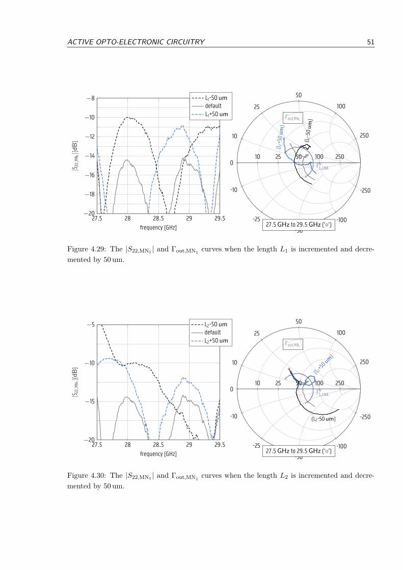
ACTIVE OPTO-ELECTRONIC CIRCUITRY 51
27.5 28 28.5 29 29.5−20
−18
−16
−14
−12
−10
−8
frequency [GHz]
|S 22,MN 1|[d
B]
L1-50 umdefaultL1+50 um
10 25 50 100 2500
10
25
50
100
250
-10
-25
-50
-100
-250
27.5GHz to 29.5GHz (‘’)
Γ∗L,LNA
Γout,MN1
(L1+50
um)
(L1-50um)
Figure 4.29: The |S22,MN1 | and Γout,MN1curves when the length L1 is incremented and decre-
mented by 50 um.
27.5 28 28.5 29 29.5−20
−15
−10
−5
frequency [GHz]
|S 22,MN 1|[d
B]
L2-50 umdefaultL2+50 um
10 25 50 100 2500
10
25
50
100
250
-10
-25
-50
-100
-250
27.5GHz to 29.5GHz (‘’)
Γ∗L,LNA
Γout,MN1
(L2-50 um)
(L 2+50 um)
Figure 4.30: The |S22,MN1 | and Γout,MN1curves when the length L2 is incremented and decre-
mented by 50 um.
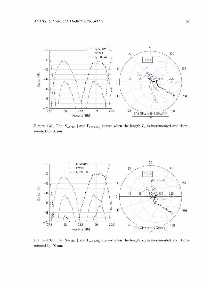
ACTIVE OPTO-ELECTRONIC CIRCUITRY 52
27.5 28 28.5 29 29.5−20
−18
−16
−14
−12
−10
−8
frequency [GHz]
|S 22,MN 1|[d
B]
L3-50 umdefaultL3+50 um
10 25 50 100 2500
10
25
50
100
250
-10
-25
-50
-100
-250
27.5GHz to 29.5GHz (‘’)
Γ ∗L,LNA
Γout,MN1
(L3 -50 um)
(L3 +50um
)
Figure 4.31: The |S22,MN1 | and Γout,MN1curves when the length L3 is incremented and decre-
mented by 50 um.
27.5 28 28.5 29 29.5−20
−18
−16
−14
−12
−10
−8
frequency [GHz]
|S 22,MN 1|[d
B]
L4-50 umdefaultL4+50 um
10 25 50 100 2500
10
25
50
100
250
-10
-25
-50
-100
-250
27.5GHz to 29.5GHz (‘’)
Γ∗L,LNA
Γout,MN1
(L4 -50 um)
(L4+50 um)
Figure 4.32: The |S22,MN1 | and Γout,MN1curves when the length L4 is incremented and decre-
mented by 50 um.
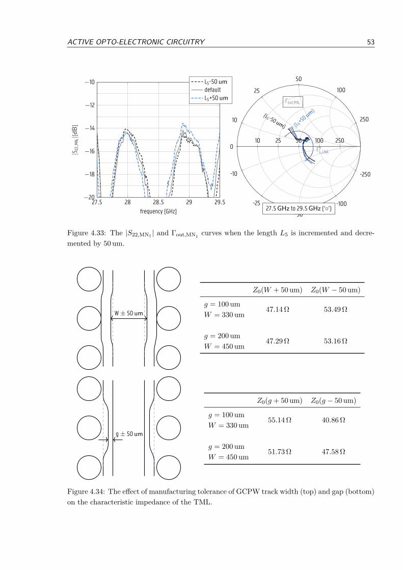
ACTIVE OPTO-ELECTRONIC CIRCUITRY 53
27.5 28 28.5 29 29.5−20
−18
−16
−14
−12
−10
frequency [GHz]
|S 22,MN 1|[d
B]
L5-50 umdefaultL5+50 um
10 25 50 100 2500
10
25
50
100
250
-10
-25
-50
-100
-250
27.5GHz to 29.5GHz (‘’)
Γ∗L,LNA
Γout,MN1
(L5 -50 um) (L 5+50
um)
Figure 4.33: The |S22,MN1 | and Γout,MN1curves when the length L5 is incremented and decre-
mented by 50 um.
W± 50 um
g± 50 um
Z0(W + 50um) Z0(W − 50 um)
g = 100 um47.14Ω 53.49Ω
W = 330 um
g = 200 um47.29Ω 53.16Ω
W = 450 um
Z0(g + 50um) Z0(g − 50 um)
g = 100 um55.14Ω 40.86Ω
W = 330 um
g = 200 um51.73Ω 47.58Ω
W = 450 um
Figure 4.34: The effect of manufacturing tolerance of GCPW track width (top) and gap (bottom)on the characteristic impedance of the TML.
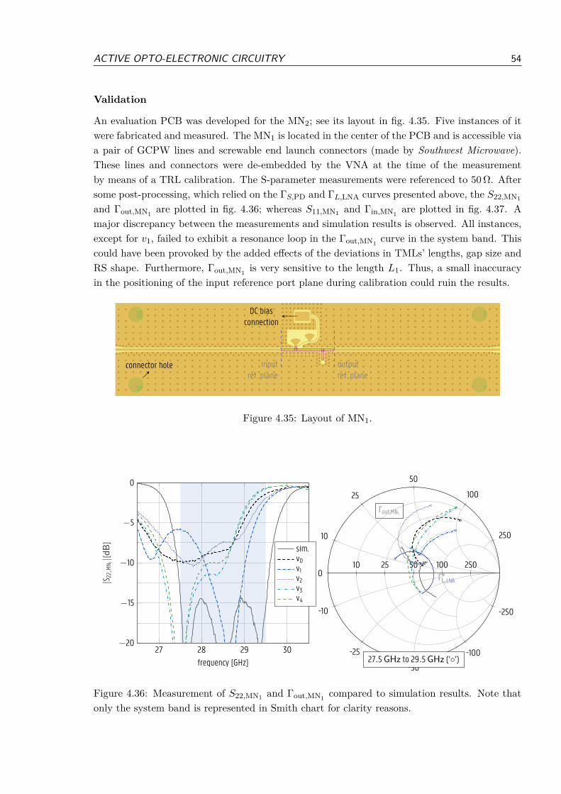
ACTIVE OPTO-ELECTRONIC CIRCUITRY 54
Validation
An evaluation PCB was developed for the MN2; see its layout in fig. 4.35. Five instances of itwere fabricated and measured. The MN1 is located in the center of the PCB and is accessible viaa pair of GCPW lines and screwable end launch connectors (made by Southwest Microwave).These lines and connectors were de-embedded by the VNA at the time of the measurementby means of a TRL calibration. The S-parameter measurements were referenced to 50 Ω. Aftersome post-processing, which relied on the ΓS,PD and ΓL,LNA curves presented above, the S22,MN1
and Γout,MN1are plotted in fig. 4.36; whereas S11,MN1 and Γin,MN1
are plotted in fig. 4.37. Amajor discrepancy between the measurements and simulation results is observed. All instances,except for v1, failed to exhibit a resonance loop in the Γout,MN1
curve in the system band. Thiscould have been provoked by the added effects of the deviations in TMLs’ lengths, gap size andRS shape. Furthermore, Γout,MN1
is very sensitive to the length L1. Thus, a small inaccuracyin the positioning of the input reference port plane during calibration could ruin the results.
connector hole
DC biasconnection
outputref. plane
inputref. plane
Figure 4.35: Layout of MN1.
27 28 29 30−20
−15
−10
−5
0
frequency [GHz]
|S 22,MN 1|[d
B]
sim.v0v1v2v3v4
10 25 50 100 2500
10
25
50
100
250
-10
-25
-50
-100
-250
27.5GHz to 29.5GHz (‘’)
Γ∗L,LNA
Γout,MN1
Figure 4.36: Measurement of S22,MN1 and Γout,MN1compared to simulation results. Note that
only the system band is represented in Smith chart for clarity reasons.
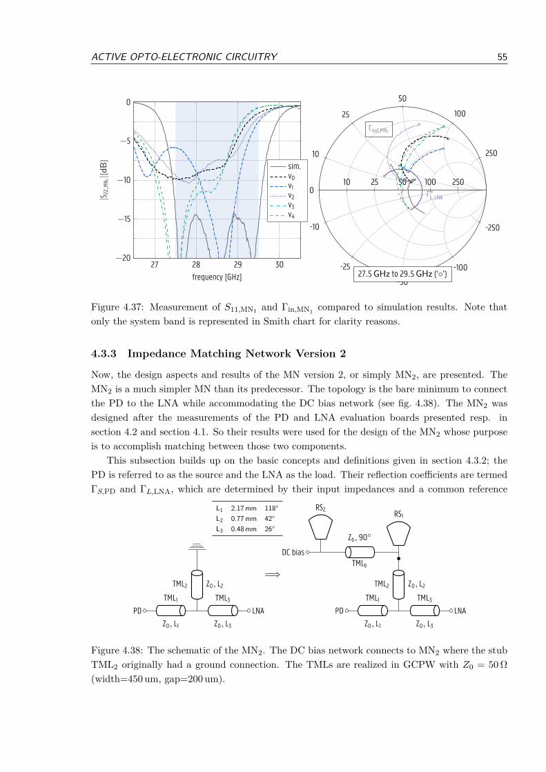
ACTIVE OPTO-ELECTRONIC CIRCUITRY 55
27 28 29 30−20
−15
−10
−5
0
frequency [GHz]
|S 22,MN 1|[d
B]
sim.v0v1v2v3v4
10 25 50 100 2500
10
25
50
100
250
-10
-25
-50
-100
-250
27.5GHz to 29.5GHz (‘’)
Γ∗L,LNA
Γout,MN1
Figure 4.37: Measurement of S11,MN1 and Γin,MN1compared to simulation results. Note that
only the system band is represented in Smith chart for clarity reasons.
4.3.3 Impedance Matching Network Version 2
Now, the design aspects and results of the MN version 2, or simply MN2, are presented. TheMN2 is a much simpler MN than its predecessor. The topology is the bare minimum to connectthe PD to the LNA while accommodating the DC bias network (see fig. 4.38). The MN2 wasdesigned after the measurements of the PD and LNA evaluation boards presented resp. insection 4.2 and section 4.1. So their results were used for the design of the MN2 whose purposeis to accomplish matching between those two components.
This subsection builds up on the basic concepts and definitions given in section 4.3.2; thePD is referred to as the source and the LNA as the load. Their reflection coefficients are termedΓS,PD and ΓL,LNA, which are determined by their input impedances and a common reference
L1 2.17 mm 118°L2 0.77 mm 42°L3 0.48 mm 26°
PDTML1
Z0, L1
TML2 Z0, L2TML3
Z0, L3
LNA
=⇒
PDTML1
Z0, L1
TML2 Z0, L2TML3
Z0, L3
LNA
RS1
TMLb
Zb, 90
RS2
DC bias
Figure 4.38: The schematic of the MN2. The DC bias network connects to MN2 where the stubTML2 originally had a ground connection. The TMLs are realized in GCPW with Z0 = 50Ω
(width=450 um, gap=200 um).
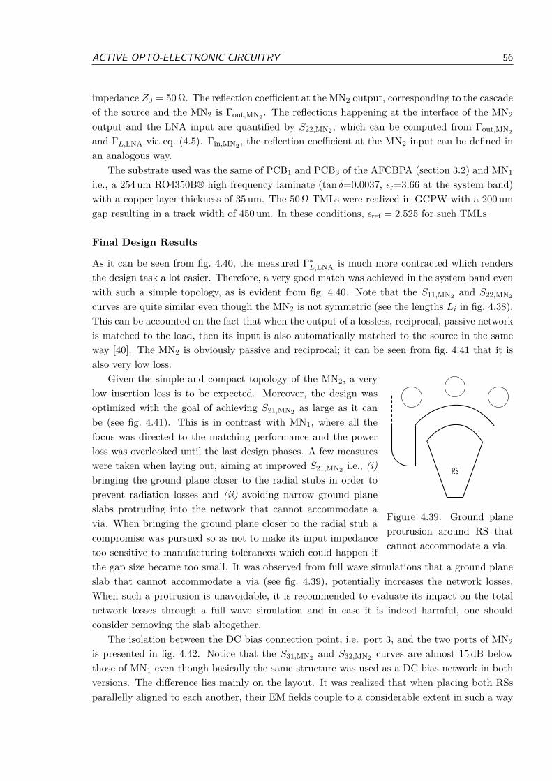
ACTIVE OPTO-ELECTRONIC CIRCUITRY 56
impedance Z0 = 50Ω. The reflection coefficient at the MN2 output, corresponding to the cascadeof the source and the MN2 is Γout,MN2
. The reflections happening at the interface of the MN2
output and the LNA input are quantified by S22,MN2 , which can be computed from Γout,MN2
and ΓL,LNA via eq. (4.5). Γin,MN2, the reflection coefficient at the MN2 input can be defined in
an analogous way.The substrate used was the same of PCB1 and PCB3 of the AFCBPA (section 3.2) and MN1
i.e., a 254 um RO4350B® high frequency laminate (tan δ=0.0037, ϵr=3.66 at the system band)with a copper layer thickness of 35 um. The 50 Ω TMLs were realized in GCPW with a 200 umgap resulting in a track width of 450 um. In these conditions, ϵref = 2.525 for such TMLs.
Final Design Results
As it can be seen from fig. 4.40, the measured Γ∗L,LNA is much more contracted which renders
the design task a lot easier. Therefore, a very good match was achieved in the system band evenwith such a simple topology, as is evident from fig. 4.40. Note that the S11,MN2 and S22,MN2
curves are quite similar even though the MN2 is not symmetric (see the lengths Li in fig. 4.38).This can be accounted on the fact that when the output of a lossless, reciprocal, passive networkis matched to the load, then its input is also automatically matched to the source in the sameway [40]. The MN2 is obviously passive and reciprocal; it can be seen from fig. 4.41 that it isalso very low loss.
RS
Figure 4.39: Ground planeprotrusion around RS thatcannot accommodate a via.
Given the simple and compact topology of the MN2, a verylow insertion loss is to be expected. Moreover, the design wasoptimized with the goal of achieving S21,MN2 as large as it canbe (see fig. 4.41). This is in contrast with MN1, where all thefocus was directed to the matching performance and the powerloss was overlooked until the last design phases. A few measureswere taken when laying out, aiming at improved S21,MN2 i.e., (i)bringing the ground plane closer to the radial stubs in order toprevent radiation losses and (ii) avoiding narrow ground planeslabs protruding into the network that cannot accommodate avia. When bringing the ground plane closer to the radial stub acompromise was pursued so as not to make its input impedancetoo sensitive to manufacturing tolerances which could happen ifthe gap size became too small. It was observed from full wave simulations that a ground planeslab that cannot accommodate a via (see fig. 4.39), potentially increases the network losses.When such a protrusion is unavoidable, it is recommended to evaluate its impact on the totalnetwork losses through a full wave simulation and in case it is indeed harmful, one shouldconsider removing the slab altogether.
The isolation between the DC bias connection point, i.e. port 3, and the two ports of MN2
is presented in fig. 4.42. Notice that the S31,MN2 and S32,MN2 curves are almost 15 dB belowthose of MN1 even though basically the same structure was used as a DC bias network in bothversions. The difference lies mainly on the layout. It was realized that when placing both RSsparallelly aligned to each another, their EM fields couple to a considerable extent in such a way

ACTIVE OPTO-ELECTRONIC CIRCUITRY 57
27.5 28 28.5 29 29.5−30
−28
−26
−24
−22
−20
−18
−16
frequency [GHz]
|S ii|[dB
]
|S22,MN2 ||S11,MN2 |
10 25 50 100 2500
10
25
50
100
250
-10
-25
-50
-100
-250
27.5GHz to 29.5GHz (‘’)
Γ∗L,LNA
Γ in,MN 1
Γ∗S,PD
Γout,MN1
Figure 4.40: The magnitude |Sii| parameters of MN2 (left); and the reflection coefficientsΓout,MN2
and Γin,MN2 of the MN2 (right).
27.5 28 28.5 29 29.5−0.4
−0.3
−0.2
−0.1
0
due to mismatch
due to copper + substrate losses =⇒√|S21|2 + |S11|2
due to radition losses
frequency [GHz]
|S 21,MN 2|[d
B]
Figure 4.41: The S21 of the MN2 broken down intothe factors due to impedance mismatch, copper anddielectric losses and radiation losses.
27.5 28 28.5 29 29.5
−54
−52
−50
−48
−46
−44
−42
−40
frequency [GHz]
|S ij|[dB
]
|S31,MN2 ||S32,MN2 |
Figure 4.42: The S31 and S32 of theMN2, where port 3 refers to the DC biasconnection point.

ACTIVE OPTO-ELECTRONIC CIRCUITRY 58
that a transmission higher than -30 dB is observed even when there is no physical connectionbetween the RSs. In order to improve the isolation, the RS2 was tilted w.r.t. the RS1 and theywere spaced as much as possible from each other.
Sensitivity Analysis
A sensitivity analysis was carried out for the MN2. The simulation results are presented infigs. 4.43 to 4.45 where the effect of the variation of the lengths L1, L2 and L3 is analyzedseparately. Due to the simplicity of such MN, the manufacturing tolerances that the lengths aresubjected to barely affect the MN2 performance.
In section 4.3.2 it was concluded that the gap size g = 100 um compromised the TMLs’ char-acteristic impedance sensitivity to manufacturing tolerances (which amounts to ±50 um) to acertain extent. Opting for g = 200 um can render the design a lot more robust to manufacturingimperfections involving the gap. The main argument for choosing a small gap is to reduce para-sitic radiation from the network (which can cause not only power loss, but also electromagneticinterference (EMI) issues). Now, the power radiated from the MN2 (as can be computed usingthe formula Prad = 10 log
(1− 10(pr/10)
)from the S21,MN2 radiation insertion loss pr shown in
fig. 4.41) is always below -18 dB. In this context, it is understood that the best decision is toconsiderably improve the robustness of MN2 to manufacturing tolerances instead of marginallyreducing the radiated power, which can be assumed to be low enough.
27.5 28 28.5 29 29.5−30
−25
−20
−15
frequency [GHz]
|S 22,MN 2|[d
B]
L1-50 umdefaultL1+50 um
10 25 50 100 2500
10
25
50
100
250
-10
-25
-50
-100
-250
27.5GHz to 29.5GHz (‘’)
Γout,MN1
Figure 4.43: The |S22,MN2 | and Γout,MN2curves when the length L1 is incremented and decre-
mented by 50 um.
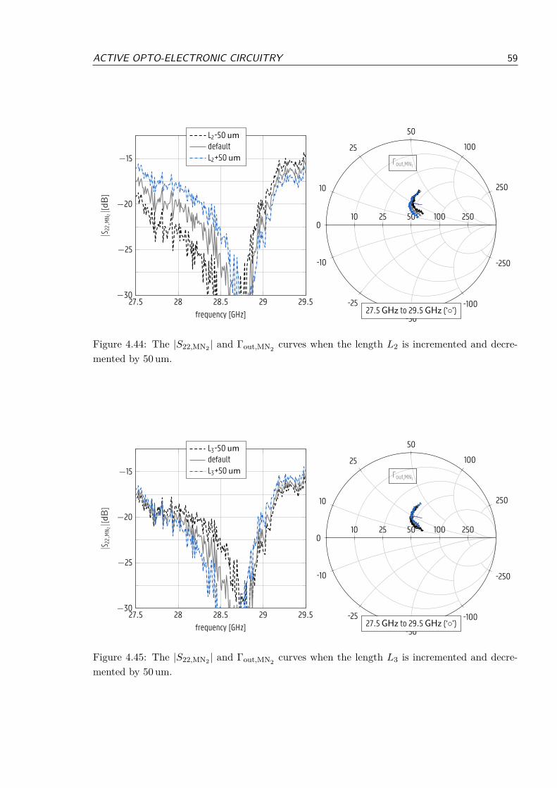
ACTIVE OPTO-ELECTRONIC CIRCUITRY 59
27.5 28 28.5 29 29.5−30
−25
−20
−15
frequency [GHz]
|S 22,MN 2|[d
B]
L2-50 umdefaultL2+50 um
10 25 50 100 2500
10
25
50
100
250
-10
-25
-50
-100
-250
27.5GHz to 29.5GHz (‘’)
Γout,MN1
Figure 4.44: The |S22,MN2 | and Γout,MN2curves when the length L2 is incremented and decre-
mented by 50 um.
27.5 28 28.5 29 29.5−30
−25
−20
−15
frequency [GHz]
|S 22,MN 2|[d
B]
L3-50 umdefaultL3+50 um
10 25 50 100 2500
10
25
50
100
250
-10
-25
-50
-100
-250
27.5GHz to 29.5GHz (‘’)
Γout,MN1
Figure 4.45: The |S22,MN2 | and Γout,MN2curves when the length L3 is incremented and decre-
mented by 50 um.
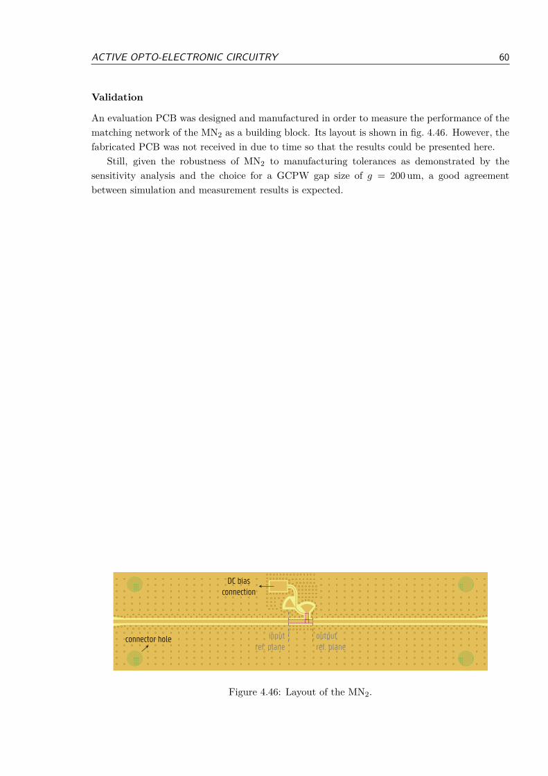
ACTIVE OPTO-ELECTRONIC CIRCUITRY 60
Validation
An evaluation PCB was designed and manufactured in order to measure the performance of thematching network of the MN2 as a building block. Its layout is shown in fig. 4.46. However, thefabricated PCB was not received in due to time so that the results could be presented here.
Still, given the robustness of MN2 to manufacturing tolerances as demonstrated by thesensitivity analysis and the choice for a GCPW gap size of g = 200 um, a good agreementbetween simulation and measurement results is expected.
connector hole
DC biasconnection
outputref. plane
inputref. plane
Figure 4.46: Layout of the MN2.
Chapter 5
Conclusion and Future Research
In this thesis, an attractive antenna for PAA applications in 5G communications has beendesigned, thoroughly analyzed and evaluated. The AFCBPA has great potential of serving asa platform for the integration of active opto-electronics so that it receives RoF optical signalsstraight from an optical beamforming network and/or is used as a RAU in small cell deployments.Evaluation proved it to be a very efficient and wideband antenna whose beamwidth of about75 degree represents a middle ground between maximum gain and beam steering capabilities.Additionally, the antenna was miniaturized achieving a functional size of ≈ λ0/2, allowing fora 80° grating-lobe-free scan angle, when the 0.5 mm clearance design rule between round-edge-plated cavities is respected. Even when the antenna elements are so closely spaced, the mutualcoupling between them is minimal thanks to the inherent self-shielding added by the cavity-backed configuration. This is specially remarkable for an AFSIW component, which is typicallylarger than its dielectric-filled counterpart. At the same time, the AFSIW cavity was responsiblefor the high (simulated) total efficiency, η >= 97.5% in the system band. Furthermore, a FTBRabove 9.3 dB was attained in the system band. The measured -10-dB-impedance band of theantenna itself ranged from 24.19 GHz to 32.33 GHz (28.4 %).
A cost effective and high performance commercial LNA operating at lower mmWave frequen-cies was selected and its S-parameters were measured by means of an evaluation board. Theresults obtained can be useful for any future work employing an LNA at such frequencies.
An in-house PD that exhibits large 3-dB bandwidth, among other features that makes itsuited for the intended application, was characterized via an evaluation PCB. This way, thereflection coefficient of the PD was obtained, which included the effect of mounting it on a PCBand wirebonding it to a GCPW track.
Two MN were investigated, i.e. MN1 and MN2 to interconnect the PD and the LNA. Inthe system band, the insertion loss of the MN2 was below 0.3 dB. Attached to the MN2 is asophisticated DC bias network that renders the MN fully decoupled at the system band. TheMN2 has not yet been validated but full-wave EM simulations indicate that the MN2 mustbe very robust to manufacturing tolerances so that a good agreement between simulation andmeasurements is expected.
It remains to co-optimize the interconnection between the active optoelectronic circuitryand the antenna, by tuning the input impedance of the latter. Then, a communication link
61

CONCLUSION AND FUTURE RESEARCH 62
will be set with the receiver antenna implemented by Bosman in [22]. The next milestone inthis research project would be to integrate both the transmit and receive circuitry on the sameantenna element.
It has been argued that the AFCBPA is suited for antenna arrays thanks, among others, toits miniaturization (Wcav ≈ λ0/2). However, the dimension of the transmitter in the y-directionis increased due to the presence of the opto-electronic circuitry. An uniform linear array (ULA)with the antennas disposed laterally could be realized with the present version. Now, in orderto employ it in planar arrays, the active electronic components needs to be integrated in a morecompact way.

Bibliography
[1] G. mobile Suppliers Association, Evolution from lte to 5g, Apr. 2018.
[2] A. Osseiran, F. Boccardi, V. Braun, K. Kusume, P. Marsch, M. Maternia, O. Queseth, M. Schell-mann, H. Schotten, H. Taoka, H. Tullberg, M. A. Uusitalo, B. Timus, and M. Fallgren, “Scenariosfor 5g mobile and wireless communications: The vision of the metis project”, IEEE CommunicationsMagazine, vol. 52, no. 5, pp. 26–35, May 2014, issn: 0163-6804. doi: 10.1109/MCOM.2014.6815890.
[3] A. Gupta and R. K. Jha, “A survey of 5g network: Architecture and emerging technologies”, IEEEaccess, vol. 3, pp. 1206–1232, 2015.
[4] T. E. Bogale and L. B. Le, “Massive mimo and millimeter wave for 5g wireless hetnet: Potentialsand challenges”, arXiv preprint arXiv:1510.06359, 2015.
[5] Y. Chen, S. Zhang, S. Xu, and G. Y. Li, “Fundamental trade-offs on green wireless networks”,IEEE Communications Magazine, vol. 49, no. 6, pp. 30–37, Jun. 2011, issn: 0163-6804. doi: 10.1109/MCOM.2011.5783982.
[6] T. Cameron, “5g—the microwave perspective”, Analog Devices Technical Article. Avaliable fromhttp://www. analog. com/media/en/technical-documentation/technical-articles/5G-The-Microwave-Perspective. pdf,
[7] G. mobile Suppliers Association et al., The road to 5g: Drivers, applications, requirements andtechnical development, Nov. 2015.
[8] J. H. Tsai, Y. C. Cheng, C. C. Hung, K. C. Chiang, and W. T. Li, “A 37-40 ghz power amplifier for5g phased array applications using 0.1-um gaas phemt process”, in 2017 IEEE 7th InternationalConference on Consumer Electronics - Berlin (ICCE-Berlin), Sep. 2017, pp. 85–87. doi: 10.1109/ICCE-Berlin.2017.8210597.
[9] A. Valdes-Garcia, B. Sadhu, X. Gu, Y. Tousi, D. Liu, S. K. Reynolds, J. Haillin, S. Sahl, and L.Rexberg, “Circuit and antenna-in-package innovations for scaled mmwave 5g phased array mod-ules”, in 2018 IEEE Custom Integrated Circuits Conference (CICC), Apr. 2018, pp. 1–8. doi:10.1109/CICC.2018.8357050.
[10] S. Yamaguchi, H. Nakamizo, S. Shinjo, K. Tsutsumi, T. Fukasawa, and H. Miyashita, “Developmentof active phased array antenna for high shf wideband massive mimo in 5g”, in 2017 IEEE Inter-national Symposium on Antennas and Propagation USNC/URSI National Radio Science Meeting,Jul. 2017, pp. 1463–1464. doi: 10.1109/APUSNCURSINRSM.2017.8072774.
[11] A. M. Zin, M. S. Bongsu, S. M. Idrus, and N. Zulkifli, “An overview of radio-over-fiber networktechnology”, in International Conference On Photonics 2010, Jul. 2010, pp. 1–3. doi: 10.1109/ICP.2010.5604429.
[12] I. Aldaya, G. Campuzano, G. Castañón, and A. Aragón-Zavala, “A tutorial on optical feeding ofmillimeter-wave phased array antennas for communication applications”, International Journal ofAntennas and Propagation, vol. 2015, 2015.
63

BIBLIOGRAPHY 64
[13] O. A. E. Caytan, L. Bogaert, H. Li, J. V. Kerrebrouck, S. Lemey, G. Torfs, J. Bauwelinck, P.Demeester, S. Agneessens, D. V. Ginste, and H. Rogier, “Passive opto-antenna as downlink remoteantenna unit for radio frequency over fiber”, Journal of Lightwave Technology, pp. 1–1, 2018, issn:0733-8724. doi: 10.1109/JLT.2018.2834153.
[14] K. Li, X. Xie, Q. Li, Y. Shen, M. E. Woodsen, Z. Yang, A. Beling, and J. C. Campbell, “High-power photodiode integrated with coplanar patch antenna for 60-ghz applications”, IEEE PhotonicsTechnology Letters, vol. 27, no. 6, pp. 650–653, Mar. 2015, issn: 1041-1135. doi: 10.1109/LPT.2015.2389652.
[15] D. Wake, N. J. Gomes, C. Lethien, C. Sion, and J. P. Vilcot, “An optically powered radio overfiber remote unit using wavelength division multiplexing”, in 2008 International Topical Meetingon Microwave Photonics jointly held with the 2008 Asia-Pacific Microwave Photonics Conference,Sep. 2008, pp. 197–200. doi: 10.1109/MWP.2008.4666670.
[16] M. Matsuura and Y. Minamoto, “Optically powered and controlled beam steering system for radio-over-fiber networks”, Journal of Lightwave Technology, vol. 35, no. 4, pp. 979–988, Feb. 2017, issn:0733-8724. doi: 10.1109/JLT.2016.2631251.
[17] A. Belenguer, H. Esteban, and V. E. Boria, “Novel empty substrate integrated waveguide forhigh-performance microwave integrated circuits”, IEEE Transactions on Microwave Theory andTechniques, vol. 62, no. 4, pp. 832–839, Apr. 2014, issn: 0018-9480. doi: 10.1109/TMTT.2014.2309637.
[18] Q. V. den Brande, S. Lemey, J. Vanfleteren, and H. Rogier, “Highly efficient impulse-radio ultra-wideband cavity-backed slot antenna in stacked air-filled substrate integrated waveguide technol-ogy”, IEEE Transactions on Antennas and Propagation, vol. 66, no. 5, pp. 2199–2209, May 2018,issn: 0018-926X. doi: 10.1109/TAP.2018.2809626.
[19] M. Mosalanejad, S. Brebels, I. Ocket, C. Soens, G. A. E. Vandenbosch, and A. Bourdoux, “Mil-limeter wave cavity backed aperture coupled microstrip patch antenna”, in 2016 10th EuropeanConference on Antennas and Propagation (EuCAP), Apr. 2016, pp. 1–5. doi: 10.1109/EuCAP.2016.7481725.
[20] A. Dierck, F. Declercq, and H. Rogier, “Review of active textile antenna co-design and optimizationstrategies”, in 2011 IEEE International Conference on RFID-Technologies and Applications, Sep.2011, pp. 194–201. doi: 10.1109/RFID-TA.2011.6068637.
[21] R. C. Johnson, Antenna Engineering Handbook. McGraw-Hill Professional, 1992, isbn: 0-07-032381-x. [Online]. Available: https://www.amazon.com/Antenna-Engineering-Handbook-Richard-Johnson/dp/007032381X?SubscriptionId=0JYN1NVW651KCA56C102&tag=techkie-20&linkCode=xm2&camp=2025&creative=165953&creativeASIN=007032381X.
[22] D. Bosman, “A 28.5 GHz active electro-optical remote antenna head for 5G reception”, Masterthesis, Universiteit Gent, 2018.
[23] C. A. Balanis, Antenna Theory: Analysis and Design, 3rd ed. Wiley-Interscience, 2005, isbn:047166782X.
[24] G. Kumar and K. Ray, Broadband microstrip antennas. Artech House, 2003.
[25] C. A. Balanis, Advanced Engineering Electromagnetics. Wiley, 2012, isbn: 978-0-470-58948-9. [On-line]. Available: https://www.amazon.com/Advanced-Engineering-Electromagnetics-Constantine-Balanis/dp/0470589485?SubscriptionId=0JYN1NVW651KCA56C102&tag=techkie-20&linkCode=xm2&camp=2025&creative=165953&creativeASIN=0470589485.

BIBLIOGRAPHY 65
[26] H. Rogier, “E022230: Antennas and propagation”, Ghent University, Gent, Belgium, course syl-labus, 2016.
[27] D. Deslandes and K. Wu, “Integrated microstrip and rectangular waveguide in planar form”, IEEEMicrowave and Wireless Components Letters, vol. 11, no. 2, pp. 68–70, Feb. 2001, issn: 1531-1309.doi: 10.1109/7260.914305.
[28] K. Wu, “Towards the development of terahertz substrate integrated circuit technology”, in 2010Topical Meeting on Silicon Monolithic Integrated Circuits in RF Systems (SiRF), Jan. 2010, pp. 116–119. doi: 10.1109/SMIC.2010.5422993.
[29] A. Belenguer, J. L. Cano, H. Esteban, E. Artal, and V. E. Boria, “Empty substrate integratedwaveguide technology for e plane high-frequency and high-performance circuits”, Radio Science,vol. 52, no. 1, pp. 49–69, 2017. doi: 10.1002/2016RS006181.
[30] K. Y. Kapusuz, S. Lemey, and H. Rogier, “Substrate independent microwave components in sub-strate integrated waveguide technology for high-performance smart surfaces”, IEEE Transactionson Microwave Theory and Techniques, 2017.
[31] F. Parment, A. Ghiotto, T. P. Vuong, J. M. Duchamp, and K. Wu, “Air-filled substrate integratedwaveguide for low-loss and high power-handling millimeter-wave substrate integrated circuits”,IEEE Transactions on Microwave Theory and Techniques, vol. 63, no. 4, pp. 1228–1238, Apr. 2015,issn: 0018-9480. doi: 10.1109/TMTT.2015.2408593.
[32] M. Himdi, J. P. Daniel, and C. Terret, “Analysis of aperture-coupled microstrip antenna usingcavity method”, Electronics Letters, vol. 25, no. 6, pp. 391–392, Mar. 1989, issn: 0013-5194. doi:10.1049/el:19890269.
[33] ——, “Transmission line analysis of aperture-coupled microstrip antenna”, Electronics Letters,vol. 25, no. 18, pp. 1229–1230, Aug. 1989, issn: 0013-5194. doi: 10.1049/el:19890824.
[34] D. M. Pozar and S. D. Targonski, “Improved coupling for aperture coupled microstrip antennas”,Electronics Letters, vol. 27, no. 13, pp. 1129–1131, Jun. 1991, issn: 0013-5194. doi: 10.1049/el:19910705.
[35] W. M. A. Wahab, S. Safavi-Naeini, and D. Busuioc, “Low cost microstrip patch antenna arrayusing planar waveguide technology for emerging millimeter-wave wireless communication”, in 201014th International Symposium on Antenna Technology and Applied Electromagnetics the AmericanElectromagnetics Conference, Jul. 2010, pp. 1–4. doi: 10.1109/ANTEM.2010.5552477.
[36] W. Abdel-Wahab, H. Al-Saedi, S. Safavi-Naeini, and Y. Wang, “Siw-integrated patch antennabacked air-filled cavity for 5g mmw appilcations”, in 2016 IEEE International Symposium onAntennas and Propagation (APSURSI), Jun. 2016, pp. 1233–1234. doi: 10 . 1109 / APS . 2016 .7696324.
[37] (2018). Cst microwave studio, CST - Computer Simulation Technology, [Online]. Available: https://www.cst.com/products/cstmws (visited on Feb. 5, 2018).
[38] J.-S. Hong and M. J. Lancaster, “Couplings of microstrip square open-loop resonators for cross-coupled planar microwave filters”, IEEE Transactions on Microwave Theory and Techniques, vol. 44,no. 11, pp. 2099–2109, Nov. 1996, issn: 0018-9480. doi: 10.1109/22.543968.
[39] HMC1040LP3CE GaAs pHEMT MMIC Low Noise amplifier, 24 - 43.5 GHz, Revision v00.0112,Analog Devices.
[40] K.-W. Yeom, Microwave Circuit Design: A Practical Approach Using ADS. Prentice Hall, 2015,isbn: 0134086783.

BIBLIOGRAPHY 66
[41] TRL calibration, 2018. [Online]. Available: http : / / na . support . keysight . com / pna / help /latest/S3_Cals/TRL_Calibration.htm.

Appendix A
Phase of S11 of an Ideal TransmissionLine
Consider an ideal transmission line of characteristic impedance Z0, terminated by a load ZL.When the port reference impedance is also Z0, the S11 can be obtained as follows,
S11 =Zin − Z0
Zin + Z0(A.1)
where Zin is the input impedance of the considered transmission line. It is given by,
Zin = Z0ZL + jZ0 tan(βl)
Z0 + jZL tan(βl)(A.2)
By introducing eq. (A.2) in eq. (A.1),
S11 = K1− j tan(βl)
1 + j tan(βl)= K
1− tan2(βl)− 2j tan(βl)
1 + tan2(βl)(A.3)
where,
K =Z0 ZL − Z2
0
Z0 ZL + Z20
Then,
ϕ = tan−1
(2 tanβl
1− tan2 βl
)= tan−1 (tan(2βl)) = 2βl (A.4)
67
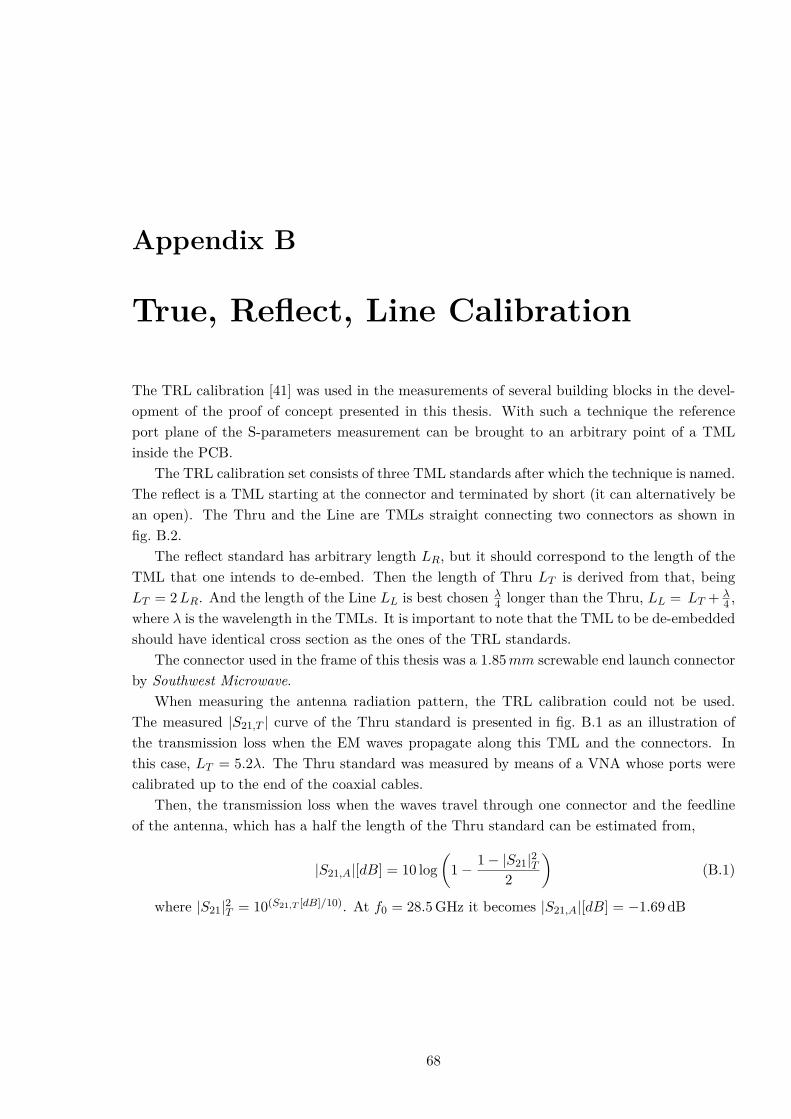
Appendix B
True, Reflect, Line Calibration
The TRL calibration [41] was used in the measurements of several building blocks in the devel-opment of the proof of concept presented in this thesis. With such a technique the referenceport plane of the S-parameters measurement can be brought to an arbitrary point of a TMLinside the PCB.
The TRL calibration set consists of three TML standards after which the technique is named.The reflect is a TML starting at the connector and terminated by short (it can alternatively bean open). The Thru and the Line are TMLs straight connecting two connectors as shown infig. B.2.
The reflect standard has arbitrary length LR, but it should correspond to the length of theTML that one intends to de-embed. Then the length of Thru LT is derived from that, beingLT = 2LR. And the length of the Line LL is best chosen λ
4 longer than the Thru, LL = LT + λ4 ,
where λ is the wavelength in the TMLs. It is important to note that the TML to be de-embeddedshould have identical cross section as the ones of the TRL standards.
The connector used in the frame of this thesis was a 1.85mm screwable end launch connectorby Southwest Microwave.
When measuring the antenna radiation pattern, the TRL calibration could not be used.The measured |S21,T | curve of the Thru standard is presented in fig. B.1 as an illustration ofthe transmission loss when the EM waves propagate along this TML and the connectors. Inthis case, LT = 5.2λ. The Thru standard was measured by means of a VNA whose ports werecalibrated up to the end of the coaxial cables.
Then, the transmission loss when the waves travel through one connector and the feedlineof the antenna, which has a half the length of the Thru standard can be estimated from,
|S21,A|[dB] = 10 log
(1−
1− |S21|2T2
)(B.1)
where |S21|2T = 10(S21,T [dB]/10). At f0 = 28.5GHz it becomes |S21,A|[dB] = −1.69 dB
68
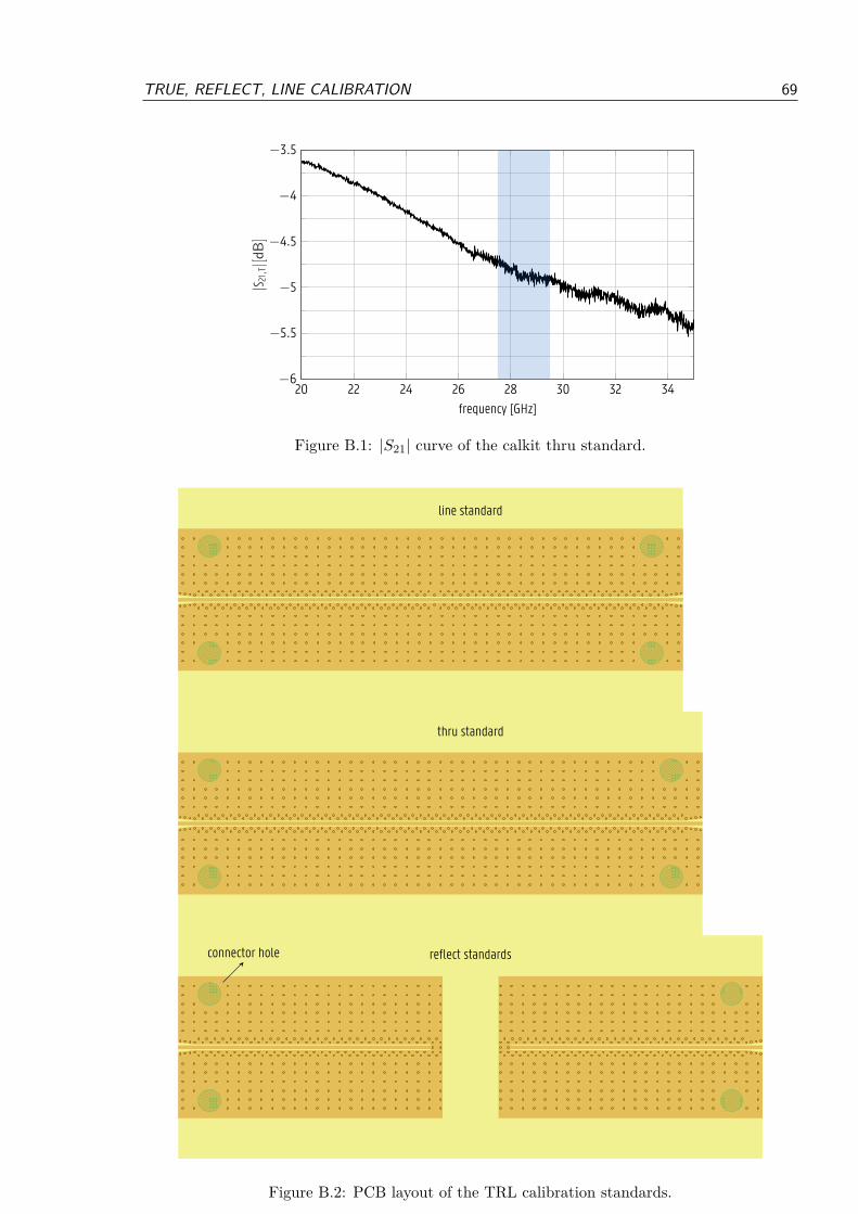
TRUE, REFLECT, LINE CALIBRATION 69
20 22 24 26 28 30 32 34−6
−5.5
−5
−4.5
−4
−3.5
frequency [GHz]
|S 21,T|[dB
]
Figure B.1: |S21| curve of the calkit thru standard.
connector hole reflect standards
thru standard
line standard
Figure B.2: PCB layout of the TRL calibration standards.


![Fundamental Limits of Correlated Fading MIMO Broadcast ...of JSDM for millimeter wave (mm-Wave) channels [23]. Assuming the ideal condition, the number of degrees of transmit correlation](https://img.pdfslide.net/doc/110x75/60d7a439e6cd8d5c964c4252/fundamental-limits-of-correlated-fading-mimo-broadcast-of-jsdm-for-millimeter.jpg)