Embed Size (px)
Citation preview
185
Analysis of Control-Loop Parameters for Effective Jamming in
Missile Borne Monopulse Receivers
Harikrishna paik
1, N.N.sastry
2, I.SantiPrabha
3
1
Dept. of E&IE, V.R.Siddhartha Engineering College, Vijayawada, Andhra Pradesh
2R&D Wing, V.R.Siddhartha Engineering College Vijayawada, Andhra Pradesh
3
E W
& G, J N T University, Kakinada, Andhra Pradesh
Abstract.
In this paper, the monopulse receiver with third order PLL (Phase Locked Loop) is designed and
the performance of the receiver is analyzed when sinusoidal CW (Continuous Wave) radar echo signal along
with CW jammer signal is applied to the receiver. In addition, when CW
FM (Frequency Modulation) signal
along with the radar echo signal is injected into the receiver, the value of modulation index for which break-
lock occurs for different values of modulating signal voltage is estimated and an empirical relation is also
obtained. The mathematical model for FM CW radar receiver is developed and implemented using Visual
System Simulator. The effectiveness
of noise jamming is also studied by injecting Phase noise and White
Gaussian noise signal into the receiver and break-lock condition of the receiver is also reported. It is shown
that break-lock in the receiver occurs when the FM modulation index (kf) exceeds 4x10⁶
without exception
with the carrier signal operating at 40 MHz and the modulating signal at 200 KHz.
Keywords: Monopulse, Radar echo, Repeat jamming.
1.
Introduction
Most of the modern missiles invariably employ monopulse receivers with PLL (Phase Locked Loop) in
frequency tracking subsystems [1]. The ability of the missile to keep the target on track depends upon its
ability to track its echo in the frequency and angle domains. Jamming of such receivers is extremely difficult
as the frequency lock and the angle servo lock requires least deviations in the repeater waveform of the
jammer and its frequency. In our earlier paper, an analysis on repeat jamming and noise jamming of the
monopulse receiver with second order PLL has been reported [2]. Spot frequency repeat jamming and Noise
jamming are analyzed in this paper for effective deception of the monopulse receiver with third order PLL
when sinusoidal CW (Continuous Wave) jammer signal and FM (Frequency Modulation) CW jammer signal
is applied to the receiver in two different cases.[3].
2.
Radar receiver with third order PLL
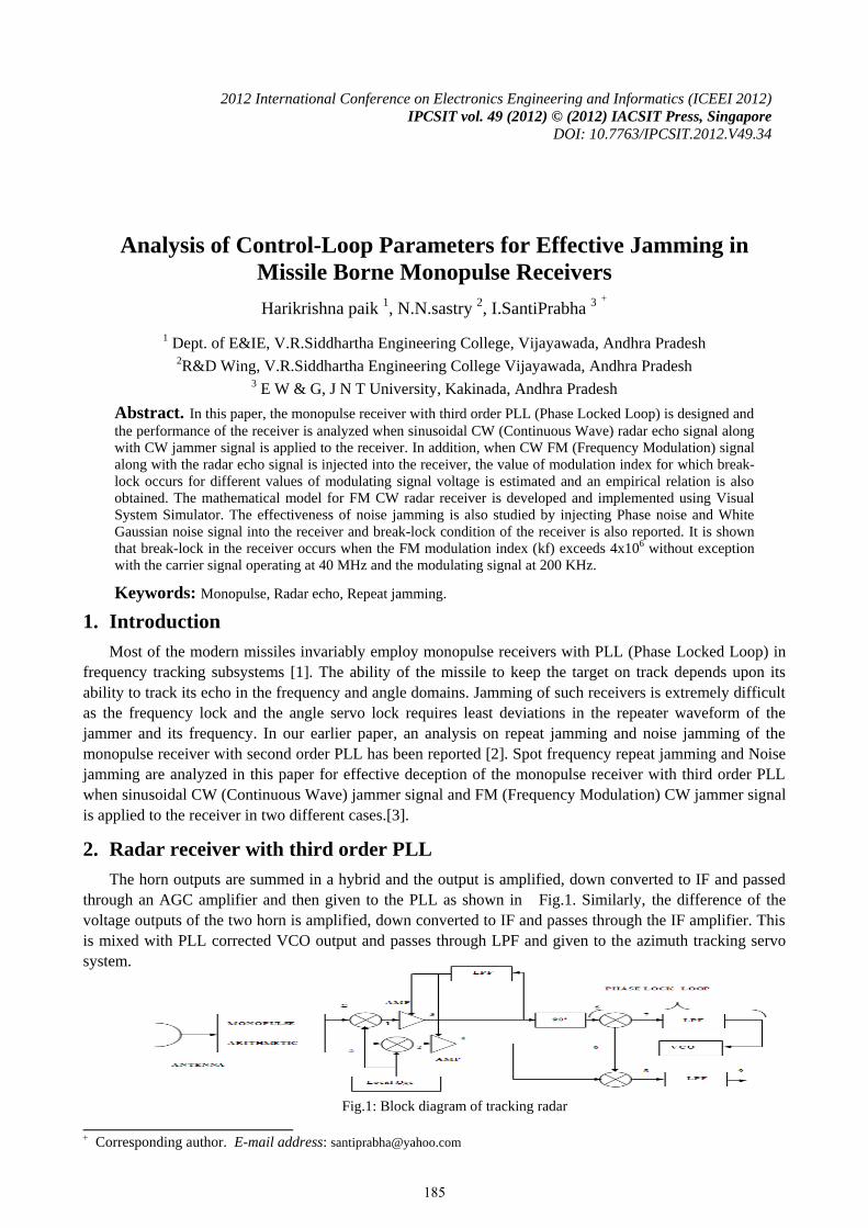
The horn outputs are summed in a hybrid and the output is amplified, down converted to IF and passed
through an AGC amplifier and then given to the PLL as shown in Fig.1. Similarly, the difference of the
voltage outputs of the two horn is amplified, down converted to IF and passes through the IF amplifier. This
is mixed with PLL corrected VCO output and passes through LPF and given to the azimuth tracking servo
system.
Corresponding author.
E-mail address:
Fig.1: Block diagram of tracking radar
2012 International Conference on Electronics Engineering and Informatics (ICEEI 2012)
IPCSIT vol. 49 (2012) © (2012) IACSIT Press, Singapore
DOI: 10.7763/IPCSIT.2012.V49 34.
186
DLY_SMPID=A1DLY=1IVAL=0
TPID=Current
TPID=Vcont
TPID=PLL_out
R
V
PFD
1
2
3
PFDCPID=C1IUP=5 mAIDN=5 mAILEAK=0 mADELAY=0 ns
TPID=radar echo
N1
2
3
DIVIDERID=C2N=2VP=1
SRC_RID=A6VAL=2COL=1TCOL= SMPFRQ=
1
2
3
VCO_BID=VCO1FRQ=60 MHzPWR=10 dBmV0=0 VKV=20e6F= V= FVTYP=Linear
SINEID=A2FRQ=30 MHzAMPL=1PHS=0 DegCTRFRQ= SMPFRQ=
C1
R2
C2
C3
R31 2
3RD_PASSID=LP1C1=0.02711 uFC2=0.3267 uFC3=0.00542 uFR2=1.319 OhmR3=4.822 Ohm
SINEID=A3FRQ=32 MHzAMPL=1.01PHS=60 DegCTRFRQ= SMPFRQ=
TPID=jammer
1
2
3
COMBINERID=S1LOSS= SIGTYP=VoltageNIN=2CTRFRQ= PRIMINP= ISOL=30 dBNOISE=RF Budget + Time Domain
Loop filter
Radar Echo
sample delay
VCO
Third order PLL with bandwidth=1 MHz
charge pump
Divider
Jammer source
Phase DetectorCombiner
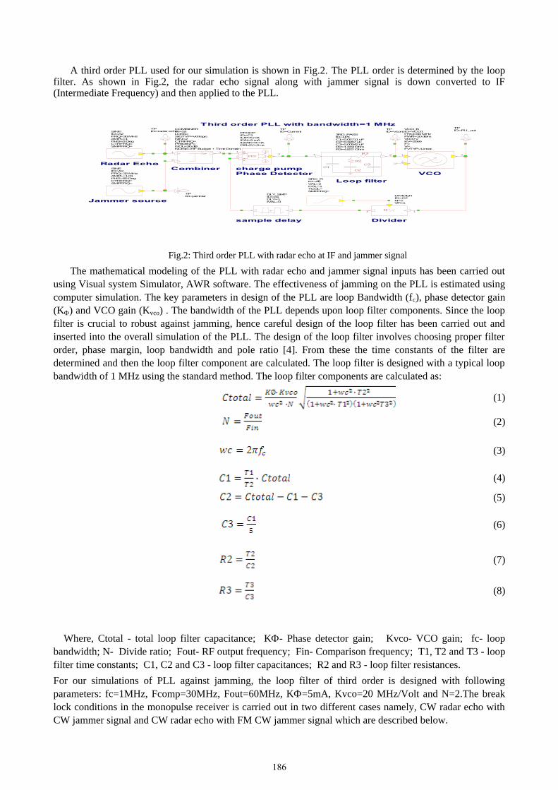
A third order PLL used for our simulation is shown in Fig.2. The PLL order is determined by the loop filter. As shown in Fig.2, the radar echo signal along with jammer signal is down converted to IF (Intermediate Frequency) and then applied to the PLL.
Fig.2: Third order PLL with radar echo at IF and jammer signal
The mathematical modeling of the PLL with radar echo and jammer signal inputs has been carried out
using Visual system Simulator, AWR software. The effectiveness of jamming on the PLL is estimated using
computer simulation. The key parameters in design of the PLL are loop Bandwidth (fc), phase detector gain
(K) and VCO gain (Kvco) . The bandwidth of the PLL depends upon loop filter components. Since the loop
filter is crucial to robust against jamming, hence careful design of the loop filter has been carried out and
inserted into the overall simulation of the PLL. The design of the loop filter involves choosing proper filter
order, phase margin, loop bandwidth and pole ratio [4]. From these the time constants of the filter are
determined and then the loop filter component are calculated. The loop filter is designed with a typical loop
bandwidth of 1 MHz using the standard method. The loop filter components are calculated as:
(1)
(2)
(3)
(4)
(5)
(6)
(7)
(8)
Where, Ctotal - total loop filter capacitance; K-
Phase detector gain;
Kvco-
VCO gain; fc-
loop
bandwidth; N- Divide ratio; Fout- RF output frequency; Fin-
Comparison frequency; T1, T2 and T3 -
loop
filter time constants; C1, C2 and C3 - loop filter capacitances; R2 and R3 -
loop filter resistances.
For our simulations of PLL against jamming, the loop filter of third order is designed with following
parameters: fc=1MHz, Fcomp=30MHz, Fout=60MHz, K=5mA, Kvco=20 MHz/Volt and N=2.The break
lock conditions in the monopulse receiver is carried out in two different cases namely, CW radar echo with
CW jammer signal and CW radar echo with FM CW jammer signal which are described below.
187
0 200 400 600 800 1000 1200 1400 1600Frequency (MHz)
input_output spectrum of PLL
-400-300-200-100
0100
Rad
ar E
cho
-400-300-200-100
0100
Jam
mer
-80-60-40-20
020
PLL
Out
put
60 MHz9.32 dBm
32 MHz8.062 dBm
30 MHz10 dBm
DB(PWR_SPEC(TP.radar echo,0.5,4,1,1,-1,0,-1,1,0,0,0,1,0)) (dBm)Real PLL System_with PFDCPDB(PWR_SPEC(TP.jammer,0.5,4,1,1,-1,0,-1,1,0,4,0,1,0)) (dBm)Real PLL System_with PFDCPDB(PWR_SPEC(TP.PLL_out,0.5,4,1,1,-1,0,-1,1,0,4,0,1,0)) (dBm)Real PLL System_with PFDCP
For J/S ratio=0.8
0 200 400 600 800 1000 1200 1400 1600Frequency (MHz)
input_output spectrum of PLL
-400-300-200-100
0100
Rad
ar E
cho
-400-300-200-100
0100
Jam
mer
-150
-100
-50
020
PLL
Out
put
64 MHz9.921 dBm
32 MHz10.09 dBm
30 MHz10 dBm
DB(PWR_SPEC(TP.radar echo,0.5,4,1,1,-1,0,-1,1,0,0,0,1,0)) (dBm)Real PLL System_with PFDCPDB(PWR_SPEC(TP.jammer,0.5,4,1,1,-1,0,-1,1,0,4,0,1,0)) (dBm)Real PLL System_with PFDCPDB(PWR_SPEC(TP.PLL_out,0.5,4,1,1,-1,0,-1,1,0,4,0,1,0)) (dBm)Real PLL System_with PFDCP
For J/S ratio=1.01
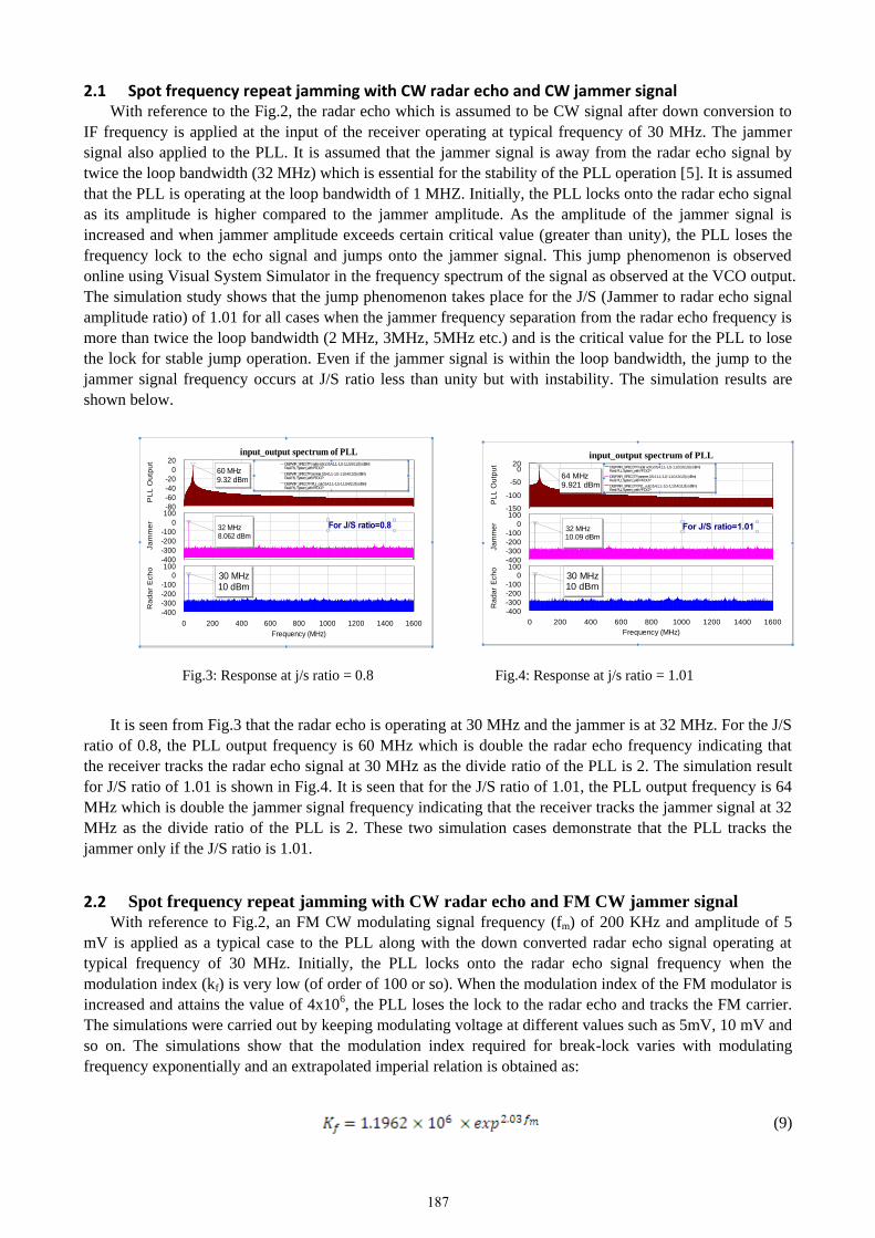
2.1 Spot frequency repeat jamming with CW radar echo and CW jammer signal With reference to the Fig.2, the radar echo which is assumed to be CW signal after down conversion to
IF frequency is applied at the input of the receiver operating at typical frequency of 30 MHz. The jammer
signal also applied to the PLL. It is assumed that the jammer signal is away from the radar echo signal by
twice the loop bandwidth (32 MHz) which is essential for the stability of the PLL operation [5]. It is assumed
that the PLL is operating at the loop bandwidth of 1 MHZ. Initially, the PLL locks onto the radar echo signal
as its amplitude is higher compared to the jammer amplitude. As the amplitude of the jammer signal is
increased and when jammer amplitude exceeds certain critical value (greater than unity), the PLL loses the
frequency lock to the echo signal and jumps onto the jammer signal. This jump phenomenon is observed
online using Visual System Simulator in the frequency spectrum of the signal as observed at the VCO output.
The simulation study shows that the jump phenomenon takes place for the J/S (Jammer to radar echo signal
amplitude ratio) of 1.01 for all cases when the jammer frequency separation from the radar echo frequency is
more than twice the loop bandwidth (2 MHz, 3MHz, 5MHz etc.) and is the critical value for the PLL to lose
the lock for stable jump operation. Even if the jammer signal is within the loop bandwidth, the jump to the
jammer signal frequency occurs at J/S ratio less than unity but with instability. The simulation results are
shown below.
Fig.3: Response at j/s ratio = 0.8 Fig.4: Response at j/s ratio = 1.01
It is seen from Fig.3 that the radar echo is operating at 30 MHz and the jammer is at 32 MHz. For the J/S
ratio of 0.8, the PLL output frequency is 60 MHz which is double the radar echo frequency indicating that
the receiver tracks the radar echo signal at 30 MHz as the divide ratio of the PLL is 2. The simulation result
for J/S ratio of 1.01 is shown in Fig.4. It is seen that for the J/S ratio of 1.01, the PLL output frequency is 64
MHz which is double the jammer signal frequency indicating that the receiver tracks the jammer signal at 32
MHz as the divide ratio of the PLL is 2. These two simulation cases demonstrate that the PLL tracks the
jammer only if the J/S ratio is 1.01.
2.2
Spot frequency repeat jamming with CW radar echo and FM CW jammer signal
With reference to Fig.2, an FM CW modulating signal frequency (fm) of 200 KHz and amplitude of 5
mV is applied as a typical case to the PLL along with the down converted radar echo signal operating at
typical frequency of 30 MHz. Initially, the PLL locks onto the radar echo signal frequency when the
modulation index (kf) is very low (of order of 100 or so). When the modulation index of the FM modulator is
increased and attains the value of 4x10⁶, the PLL loses the lock to the radar echo and tracks the FM carrier.
The simulations were carried out by keeping modulating voltage at different values such as 5mV, 10 mV and
so on. The simulations show that the modulation index required for break-lock varies with modulating
frequency exponentially and an extrapolated imperial relation is obtained as:
(9)
188
0 100 200 300 400 500 600 700 800 900 1000 1100 1200Frequency (MHz)
fm_spectrum
-400-300-200-100
0100
Rad
ar E
cho
-150-100-50
050
FM
Car
rier
-150
-100
-50
020
PLL
Out
put
60 MHz10 dBm
40 MHz9.999 dBm
30 MHz10 dBm
DB(PWR_SPEC(TP.fm input,1,4,1,1,-1,0,-1,1,0,0,0,1,0)) (dBm)3rd order PLL_ FM input
DB(PWR_SPEC(TP.Radar Echo,1,4,1,1,-1,0,-1,1,0,4,0,1,0)) (dBm)3rd order PLL_ FM inputDB(PWR_SPEC(TP.PLL_out,10,4,1,1,-1,0,-1,1,0,4,0,1,0)) (dBm)3rd order PLL_ FM input
fm=200KHzVm=5mVKf=1e6
0 100 200 300 400 500 600 700 800 900 1000 1100 1200Frequency (MHz)
fm_spectrum
-400-300-200-100
0100
Rad
ar E
cho
-150-100
-500
50
FM
Car
rier
-150
-100
-50
020
PLL
Out
put
80 MHz9.881 dBm
40 MHz9.994 dBm
30 MHz10 dBm
DB(PWR_SPEC(TP.fm input,1,4,1,1,-1,0,-1,1,0,0,0,1,0)) (dBm)3rd order PLL_ FM inputDB(PWR_SPEC(TP.Radar Echo,1,4,1,1,-1,0,-1,1,0,4,0,1,0)) (dBm)3rd order PLL_ FM inputDB(PWR_SPEC(TP.PLL_out,10,4,1,1,-1,0,-1,1,0,4,0,1,0)) (dBm)3rd order PLL_ FM input
fm=200KHzVm=5mVKf=4e6
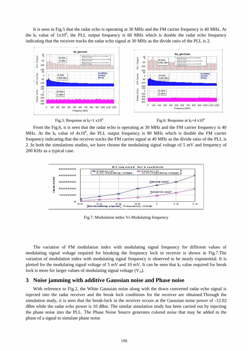
It is seen in Fig.5 that the radar echo is operating at 30 MHz and the FM carrier frequency is 40 MHz. At
the kf value of 1x10⁶, the PLL output frequency is 60 MHz which is double the radar echo frequency
indicating that the receiver tracks the radar echo signal at 30 MHz as the divide ratio of the PLL is 2.
Fig.5: Response at kf=1 x10⁶ Fig.6: Response at kf=4 x10⁶
From the Fig.6, it is seen that the radar echo is operating at 30 MHz and the FM carrier frequency is 40
MHz. At the kf value of 4x10⁶, the PLL output frequency is 80 MHz which is double the FM carrier
frequency indicating that the receiver tracks the FM carrier signal at 40 MHz as the divide ratio of the PLL is
2. In both the simulations studies, we have chosen the modulating signal voltage of 5 mV and frequency of
200 KHz as a typical case.
Fig.7: Modulation index Vs Modulating frequency
The variation of FM modulation index with modulating signal frequency for different values of
modulating signal voltage required for breaking the frequency lock in receiver is shown in Fig.7.The
variation of modulation index with modulating signal frequency is observed to be nearly exponential. It is
plotted for the modulating signal voltage of 5 mV and 10 mV. It can be seen that kf value required for break
lock is more for larger values of modulating signal voltage (Vm).
3 Noise jamming with additive Gaussian noise and Phase noise
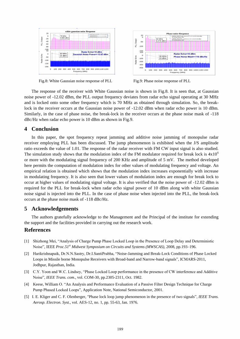
With reference to Fig.2, the White Gaussian noise along with the down converted radar echo signal is
injected into the radar receiver and the break lock conditions for the receiver are obtained.Through the
simulation study, it is seen that the break-lock in the receiver occurs at the Gaussian noise power of -12.02
dBm while the radar echo power is 10 dBm. The similar simulation study has been carried out by injecting
the phase noise into the PLL. The Phase Noise Source generates colored noise that may be added to the
phase of a signal to simulate phase noise
189
0 100 200 300 400 500 600 700 800 900 1000 1100 1200Frequency (MHz)
Phase noise Response
-400
-300
-200
-100
0
100
Rada
r Ech
o
-150
-100
-50
020
PLL
Outp
ut 40 MHz9.276 dBm
30 MHz10 dBm
DB(PWR_SPEC(TP.radar echo,2,4,1,1,-1,0,-1,1,0,4,0,1,0)) (dBm)PLL System_phase noise
DB(PWR_SPEC(TP.PLL_out,10,4,1,1,-1,0,-1,1,0,4,0,1,0)) (dBm)PLL System_phase noise
Phase Noise Mask=-118 dBc/Hz
Radar Echo=10 dBm
0 100 200 300 400 500 600 700 800 900 1000 1100 1200Frequency (MHz)
white gaussian noise Response
-200
-150
-100
-50
0
50
Rad
ar E
cho
-100-80-60-40-20
020
PLL
Out
put 70 MHz
9.865 dBm
30 MHz10 dBm
DB(PWR_SPEC(TP.radar echo,1,4,1,1,-1,0,-1,1,0,4,0,1,0)) (dBm)PLL System_Gaussian noiseDB(PWR_SPEC(TP.PLL_out,10,4,1,1,-1,0,-1,1,0,4,0,1,0)) (dBm)PLL System_Gaussian noise
Gaussian Noise Power=-12.02 dBm
Radar Echo=10 dBm
Fig.8: White Gaussian noise response of PLL Fig.9: Phase noise response of PLL
The response of the receiver with White Gaussian noise is shown in Fig.8. It is seen that, at Gaussian
noise power of -12.02 dBm, the PLL output frequency deviates from radar echo signal operating at 30 MHz
and is locked onto some other frequency which is 70 MHz as obtained through simulation. So, the break-
lock in the receiver occurs at the Gaussian noise power of -12.02 dBm when radar echo power is 10 dBm.
Similarly, in the case of phase noise, the break-lock in the receiver occurs at the phase noise mask of -118
dBc/Hz when radar echo power is 10 dBm as shown in Fig.9.
4 Conclusion
In this paper, the spot frequency repeat jamming and additive noise jamming of monopulse radar
receiver employing PLL has been discussed. The jump phenomenon is exhibited when the J/S amplitude
ratio exceeds the value of 1.01. The response of the radar receiver with FM CW input signal is also studied.
The simulation study shows that the modulation index of the FM modulator required for break lock is 4x10⁶
or more with the modulating signal frequency of 200 KHz and amplitude of 5 mV. The method developed
here permits the computation of modulation index for other values of modulating frequency and voltage. An
empirical relation is obtained which shows that the modulation index increases exponentially with increase
in modulating frequency. It is also seen that lower values of modulation index are enough for break lock to
occur at higher values of modulating signal voltage. It is also verified that the noise power of -12.02 dBm is
required for the PLL for break-lock when radar echo signal power of 10 dBm along with white Gaussian
noise signal is injected into the PLL. In the case of phase noise when injected into the PLL, the break-lock
occurs at the phase noise mask of -118 dBc/Hz.
5 Acknowledgements
The authors gratefully acknowledge to the Management and the Principal of the institute for extending
the support and the facilities provided in carrying out the research work.
References
[1] Shizhong Mei, “Analysis of Charge Pump Phase Locked Loop in the Presence of Loop Delay and Deterministic
Noise”, IEEE Proc.51st Midwest Symposium on Circuits and Systems (MWSCAS), 2008, pp.193–196.
[2] Harikrishnapaik, Dr.N.N.Sastry, Dr.I.SantiPrabha, “Noise-Jamming and Break-Lock Conditions of Phase Locked
Loops in Missile borne Monopulse Receivers with Broad-band and Narrow-band signals”, ICMARS-2011,
Jodhpur, Rajasthan, India.
[3] C.Y. Yoon and W.C. Lindsey, “Phase Locked Loop performance in the presence of CW interference and Additive
Noise”, IEEE Trans. com., vol. COM-30, pp.2305-2311, Oct. 1982.
[4] Keese, William O. “An Analysis and Performance Evaluation of a Passive Filter Design Technique for Charge
Pump Phased Locked Loops”, Application Note, National Semiconductor, 2001.
[5] I. E. Kliger and C. F. Olenberger, "Phase lock loop jump phenomenon in the presence of two signals”, IEEE Trans.
Aerosp. Electron. Syst., vol. AES-12, no. 1, pp. 55-63, Jan. 1976.