Embed Size (px)
Citation preview

Mitigating Voltage Drop in Resistive Memories by Dynamic RESETVoltage Regulation and Partition RESET
Farzaneh Zokaee Lei Jiang
Indiana University [email protected] [email protected]
Abstract—The emerging resistive random access memory(ReRAM) technology has been deemed as one of the mostpromising alternatives to DRAM in main memories, due to itsbetter scalability, zero cell leakage and short read latency. Thecross-point (CP) array enables ReRAM to obtain the theoreticalminimum 4F2 cell size by placing a cell at the cross-point ofa word-line and a bit-line. However, ReRAM CP arrays sufferfrom large sneak current resulting in significant voltage drop thatgreatly prolongs the array RESET latency. Although prior worksreduce the voltage drop in CP arrays, they either substantiallyincrease the array peripheral overhead or cannot work well withwear leveling schemes.
In this paper, we propose two array micro-architecture leveltechniques, dynamic RESET voltage regulation (DRVR) andpartition RESET (PR), to mitigate voltage drop on both bit-lines and word-lines in ReRAM CP arrays. DRVR dynamicallyprovides higher RESET voltage to the cells far from the writedriver and thus encountering larger voltage drop on a bit-line, sothat all cells on a bit-line share approximately the same latencyduring RESETs. PR decides how many and which cells to resetonline to partition the CP array into multiple equivalent circuitswith smaller word-line resistance and voltage drop. BecauseDRVR and PR greatly reduce the array RESET latency, theReRAM-based main memory lifetime under the worst case non-stop write traffic significantly decreases. To increase the CParray endurance, we further upgrade DRVR by providing lowerRESET voltage to the cells suffering from less voltage drop ona word-line. Our experimental results show that, compared tothe combination of prior voltage drop reduction techniques, ourDRVR and PR improve the system performance by 11.7% anddecrease the energy consumption by 46% averagely, while stillmaintaining > 10-year main memory system lifetime.
I. INTRODUCTION
Resistive random access memory (ReRAM), a promising non-
volatile memory technology, is projected to replace a substantial
portion of traditional DRAM in future scalable main memory
systems [1]–[3]. Through the cross-point (CP) array architecture
and vertical access device [1], ReRAM achieves the theoretical
minimum 4F2 cell size beyond 10nm. Moreover, ReRAM
obtains small write power and better-than-PCM endurance [1],
[3] by bipolar switching writes. Due to sneak current and
voltage (IR) drop, however, the ReRAM RESET latency is
orders of magnitude longer than DRAM write latency. The long
RESET latency has become a major obstacle to the construction
of ReRAM-based memory systems.
The CP array architecture [1], [4], [5] enables the 4F2 cell
on ReRAMs by placing a cell at the cross-point of a word-line
(WL) and a bit-line (BL), but it also inevitably introduces
large sneak current. In a CP array, the selected cells are not
isolated from the unselected cells. Activating a WL and a
BL in a CP array generates sneak current flow across all the
unselected cells on the selected WL and BL. To diminish sneak
current, each ReRAM cell integrates a vertical access device [4],
[6] under the memory element. Only the access devices of
selected cells are turned ON during each access. To implement
low power bipolar ReRAM switching that alternates SET and
RESET voltage polarities, an ideal access device must have
super high nonlinear selectivity at both polarities. Although
most realistic bipolar access devices keep sneak current in
check under small read voltage [1], [4], a CP array built with
these access devices still suffers from significant sneak current
during RESETs, because of the high RESET voltage. Large
sneak current produces non-trivial voltage drop on the selected
cell under a RESET. Because the ReRAM RESET latency is
inversely exponentially proportional to the voltage drop [1],
[7] on the cell, the cell voltage drop substantially prolongs
the CP array RESET latency, and thus degrades the system
performance.
It is very challenging to effectively mitigate voltage drop
and accelerate RESETs in ReRAM CP arrays. Prior work relies
on both hardware- and system-based techniques to reduce the
voltage drop. However, hardware-based schemes significantly
increase the peripheral overhead and lower the density of
CP arrays. By adding an extra copy of row decoders, one
WL in a CP array can have two grounds during RESETs, so
the WL voltage drop decreases [1]. Integrating another copy
of column multiplexers and write drivers (WDs) into a CP
array also makes RESETs can happen from two ends of a
BL [8], thereby decreasing the BL voltage drop. Redundant
dummy BLs [4] are added into a CP array, and reset to divide
the array into multiple equivalent circuits with smaller WL
resistance when there is no RESET required in their column
multiplexers. This dummy-BL scheme greatly increases the
peak RESET power and the charge pump overhead in a ReRAM
chip. Furthermore, system-based techniques are not compatible
with the wear leveling schemes and thus degrade the main
memory system lifetime. Although the ideal ReRAM cell
endurance is 1012-write [9], the over-RESET ReRAM cells
can tolerate only 106-write [10]. To maintain long enough
main memory lifetime, both inter-line [11] and intra-line [12]
wear leveling schemes are indispensable in ReRAM CP arrays.
Different WLs and BLs in a CP array suffer from distinctive
amounts of voltage drop, so recent works [13], [14] re-map and
schedule write-intensive memory lines to array regions with
less voltage drop and shorter RESET latency. These scheduling-
based techniques cannot work with the inter-line wear leveling
Authorized licensed use limited to: Indiana University. Downloaded on July 03,2020 at 14:28:08 UTC from IEEE Xplore. Restrictions apply.

(a) A ReRAM cell. (b) Bipolar switching. (c) Access device J-V.
(d) A CP array.
Ω
(e) Rwire per junction.
Fig. 1: The ReRAM technology and its CP array.
that evenly distributes hot memory lines in the entire ReRAM
CP array. Low resistance state (LRS) ReRAM cells worsen
voltage drop by creating larger sneak current. The row-biased
data layout [15] is proposed to evenly distribute LRS cells
to all BLs, but the intra-line wear leveling destroys the data
layout by randomly shifting heavily written words on a WL.In this paper, we propose array micro-architecture techniques
to mitigate voltage drop in ReRAM CP arrays.• We propose dynamic RESET voltage regulation (DRVR)
to provide higher RESET voltage to the cells far from
the write driver on a BL to compensate their voltage
drop, so that all cells on a BL can have approximately
the same effective RESET voltage and RESET latency.
Instead of a static voltage, according to the cell position
on a BL, DRVR adjusts the RESET voltage to avoid the
over-RESET reducing the cell endurance and mitigate the
voltage drop prolonging RESET latency.
• We present partition RESET (PR) to accelerate RESETs
by dynamically deciding how many and which cells to
reset on a WL to partition the CP array into multiple
equivalent circuits with smaller WL resistance and voltage
drop. PR keeps the total RESET current on a WL in check
and prevents large voltage drop on the WL by avoiding
resetting too many cells concurrently.
• Due to DRVR and PR shortening the array RESET latency,
the memory system lifetime under the worst case non-stop
write traffic significantly decreases. We upgrade DRVR
to enhance the array endurance by supplying smaller
RESET voltage to the over-RESET cells on a WL without
increasing the array RESET latency. The upgraded DRVR
guarantees >10-year lifetime for the ReRAM-based main
memory system.
• We evaluated our proposed techniques and compared them
to state-of-the-art voltage drop reduction schemes for
ReRAM CP arrays. Our results show DRVR and PR
are orthogonal designs that together mitigate the voltage
drop issue on both BLs and WLs of ReRAM CP arrays.
Averagely, DRVR and PR improve the system performance
by 11.7% and decrease the energy consumption by 46%
with small hardware overhead.
II. BACKGROUND
A. ReRAM TechnologyCell. A ReRAM cell illustrated in Figure 1a records data
by a thin metal-oxide (e.g., TaOx) layer sandwiched by a top
electrode (TE) and a bottom electrode (BE). In the metal-
oxide layer, a SET (storing “1”) produces conductive filaments
(CFs) resulting in a low resistance state (LRS) cell, while a
RESET (writing “0”) yields a high resistance state (HRS) cell
by rupturing CFs [1]. A SET generates CFs by drifting oxygen
ions to the anode layer and leaving oxygen vacancies in the
metal-oxide layer. Oxygen ions are pushed to the metal-oxide
layer by the electric field, and then recombined with oxygen
vacancies during a RESET, so the CFs are destroyed by a
RESET and the cell changes to HRS.
ReRAM switching. ReRAM relies on two methods of
resistance switching [16] that differ in the polarities of SET
and RESET. In unipolar switching, both SET and RESET
occur under positive voltage, while the polarities of SET and
RESET must be alternated in bipolar switching shown in
Figure 1b. Unipolar switching is explained by the Joule heating
acceleration of redox transitions at the basis of CF formation
and rupture in the gap region. In contrast, bipolar switching is
caused by the electric field assisted ionic migration. A bipolar
switching ReRAM cell generally requires smaller write current
and voltage, thereby consuming less write energy. A cell also
exhibits longer endurance [17] owing to less material loss
during bipolar writes. A bipolar switching cell can tolerate
106 ∼ 1012 writes [4], [9], [18], while a unipolar switching
one stands for only 105 writes [19]. Bipolar switching [20]
also completes faster than unipolar switching on a cell. So we
focus on bipolar switching ReRAM in this paper. Unlike the
power supply voltage (Vdd), the ReRAM write voltage does
not reduce, as the process technology scales. Recent ReRAM
chips [4], [5], [21] adopt on-chip charge pumps to bridge the
gap between Vdd and their SET/RESET voltage.
Fig. 2: Accessing a ReRAM CP array.
Bipolar access device. Unlike unipolar switching ReRAM
using a simple unidirectional diode [5], bipolar switching
ReRAM requires a more sophisticated bipolar access device [6]
with nonlinear selectivity at both polarities, e.g., a metal-
amorphous Si-metal (MASiM) selector or a mixed ionic elec-
tronic conduction (MIEC) access device. Figure 1c highlights
the relationship between the current density (J) and voltage
Authorized licensed use limited to: Indiana University. Downloaded on July 03,2020 at 14:28:08 UTC from IEEE Xplore. Restrictions apply.

Metric Description Value
Ion cell current of a LRS ReRAM during RESET 90uAKr nonlinear selectivity of the selector 1000A mat size: A WLs × A BLs 512n number of bits to read/write 8
Rwire wire resistance between adjacent cells 11.5ΩVrst /Vset full selected voltage during RESETs/SETs 3V
Vrd read voltage 1.8VTABLE I: The ReRAM cell, CP array and bank models.
(V ) of a bipolar selector. It supports the symmetrical current
(I) & V . A bipolar access device with larger J is critical to
the ReRAM scalability, since it still can delivery large enough
write current as the process technology scales.
Fig. 3: The ReRAM CP array architecture.
B. Cross-Point Array Architecture
Cross-point array. To implement the theoretical minimum
4F2 cell size, ReRAM adopts a cross-point (CP) array archi-
tecture [1], [5], [6] shown in Figure 1d that consists of bit-
lines (BLs) and word-lines (WLs) at upper and lower planes
perpendicular to each other. A cell stacked upon a vertical
bipolar access device is implemented at a crossing point of
these wires. Although it is possible to stack multiple CP layers
into a 3D XPoint structure to further enhance the array density,
the 3D XPoint arrays [4], [5], [22] greatly prolong the ReRAM
read/write latency to ∼ 10μs. Therefore, typically they are
used to implement SSD disks [5], [22]. In this paper, we focus
on a ReRAM-based main memory system [1]–[3] built by 2D
CP arrays.
Read and write. Figure 2 describes our ReRAM CP array
access scheme. For smaller write power and longer memory
endurance, we adopted Flip-N-Write [23] to write only changed
cells during each write. Because of the different polarities
of SET and RESET, the bipolar ReRAM write [1], [4] is
divided into a SET phase and a RESET phase. Only after all
SETs finish, RESETs can start. Besides that the operation (i.e.,
read, SET, and RESET) voltage is fully applied across the
fully-selected cells, the half-selected cells also confront partial
voltage causing the sneak current in the array. A read in a CP
array drives the selected WL to Va =Vdd and senses the current
change on the selected BL (Vb =Vbl) [24]. All unselected WLs
and BLs during a read are set to the ground (Vc = 0). The read
sneak current is not significant in a moderate size array [1], [8],
[13] typically used in a main memory system. To reset (set) a
cell in a bipolar switching CP array, the selected WL and BL
are set to Va = 0 (Va =Vset ) and Vb =Vrst (Vb = 0) respectively,
while all unselected WLs and BLs are charged to Vc =Vrst
2
(Vc =Vset
2 ) [6]. The other end of the unselected WLs are left
floating. Particularly, the half-selected cells during RESETs
generate large sneak current in a CP array.
Voltage drop, RESET latency and cell endurance. As
the process technology scales, the BL and WL resistance
in a CP array exponentially increases [25] as shown in
Figure 1e. Considering the large sneak current, it is inevitable
for CP arrays to suffer from significant voltage drop during
RESETs. Moreover, the ReRAM RESET latency is inversely
exponentially proportional to the voltage drop [1], [7], e.g., a
0.4V voltage drop can increase the ReRAM RESET latency
by 10× [7]. The RESET latency can be computed as follows:
Trst =β
ekVd(1)
, where Trst means the RESET latency, β and k are fitting
constants, and Vd denotes the voltage drop [1]. As Figure 1b
shows, if a voltage drop reduces the RESET/SET voltage to <1.7V [26], a write failure happens. There is also a trade-off [3]
between the ReRAM RESET latency and its cell endurance,
i.e., the cell endurance decreases when its RESET latency
shortens. The ReRAM cell endurance is calculated as:
Endurance = (Trst
T0)C (2)
, where T0 and C are fitting constants. Typically, C = 3 [3]. In
short, the voltage drop increases the ReRAM RESET latency
and prolongs its cell endurance in a CP array.
Over-RESET. Based on Equation 1 and 2, a large RESET
voltage greatly shortens the cell RESET latency but reduces the
cell endurance exponentially. This is so-called “over-RESET”.
Over-RESET is the dominant factor deciding the endurance of
a cell [3], [27].
C. Main Memory Baseline Modeling
Array and bank modeling. The key parameters of our
ReRAM cell, CP array and bank models are shown in Table I.
We derived the ReRAM cell Verilog-A model and its bipolar
access device MASiM parameters from a recent ReRAM
chip prototype [4]. Among state-of-the-art access devices,
MASiM [4], [6], [28] can achieve both high current density
and high bipolar nonlinear selectivity. A ReRAM cell with no
voltage drop can tolerate 5×10⁶ [3] writes and need 15ns [9]
for a RESET. We built our array and bank models mainly based
on [1]. The ReRAM CP array is built by the 20nm technology,
and its wire resistance is adopted from [25]. To balance the
trade-off between array area efficiency, read latency, and write
power, a recent array design exploration [1] sets the MAT size
to 512×512, and makes each MAT support an 8-bit data path.
To study the worst case voltage drop, we pessimistically assume
all cells in an array are in LRS. We set the read/SET/RESET
voltage as 1.8V /3V /3V . The ReRAM bank architecture can be
viewed in Figure 3, where hierarchical (i.e., global and local)
BLs and WLs are used to avoid long wires in an array. We
reported a comprehensive design space exploration on the key
parameters of our ReRAM-based main memory in §VI.
Charge pump modeling in a chip. Due to the voltage
difference between Vdd and write voltages, the state-of-the-art
Authorized licensed use limited to: Indiana University. Downloaded on July 03,2020 at 14:28:08 UTC from IEEE Xplore. Restrictions apply.
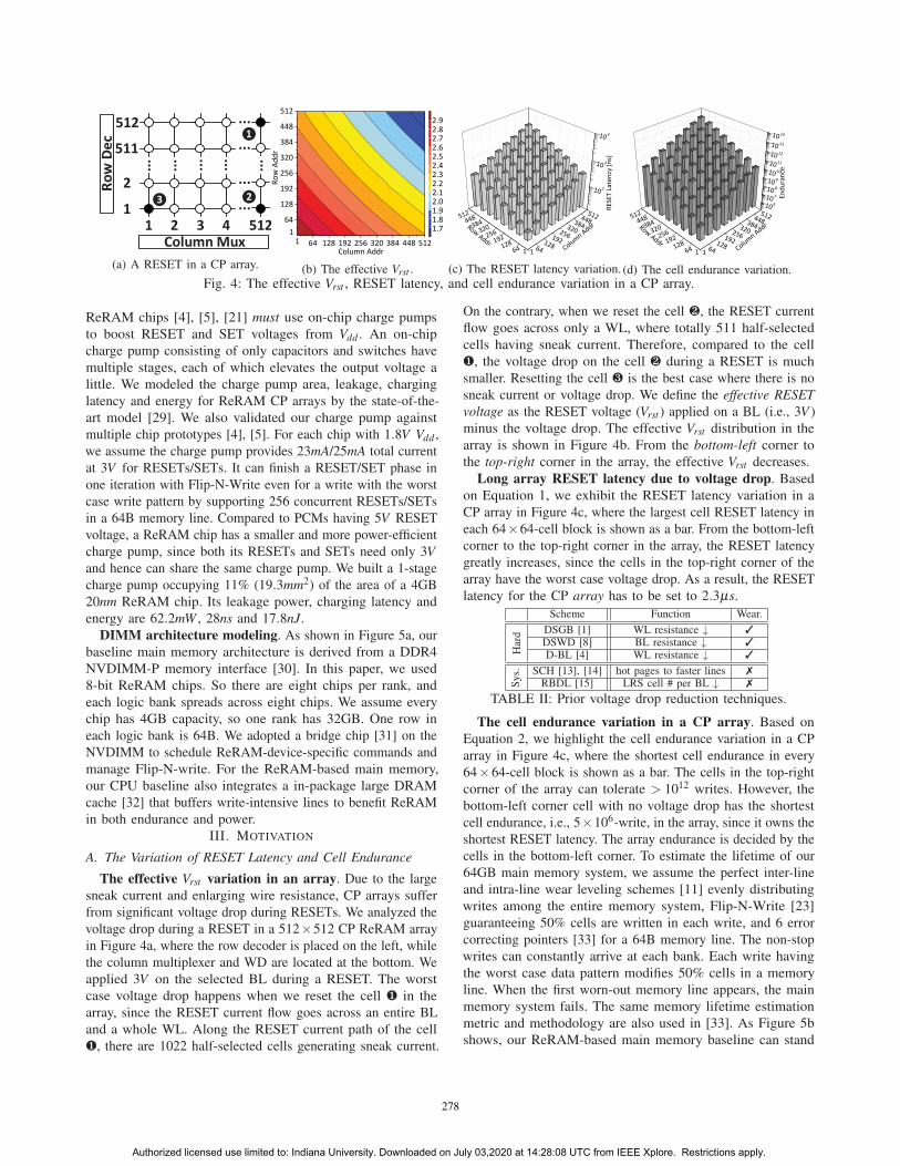
(a) A RESET in a CP array. (b) The effective Vrst . (c) The RESET latency variation. (d) The cell endurance variation.Fig. 4: The effective Vrst , RESET latency, and cell endurance variation in a CP array.
ReRAM chips [4], [5], [21] must use on-chip charge pumps
to boost RESET and SET voltages from Vdd . An on-chip
charge pump consisting of only capacitors and switches have
multiple stages, each of which elevates the output voltage a
little. We modeled the charge pump area, leakage, charging
latency and energy for ReRAM CP arrays by the state-of-the-
art model [29]. We also validated our charge pump against
multiple chip prototypes [4], [5]. For each chip with 1.8V Vdd ,
we assume the charge pump provides 23mA/25mA total current
at 3V for RESETs/SETs. It can finish a RESET/SET phase in
one iteration with Flip-N-Write even for a write with the worst
case write pattern by supporting 256 concurrent RESETs/SETs
in a 64B memory line. Compared to PCMs having 5V RESET
voltage, a ReRAM chip has a smaller and more power-efficient
charge pump, since both its RESETs and SETs need only 3Vand hence can share the same charge pump. We built a 1-stage
charge pump occupying 11% (19.3mm2) of the area of a 4GB
20nm ReRAM chip. Its leakage power, charging latency and
energy are 62.2mW , 28ns and 17.8nJ.
DIMM architecture modeling. As shown in Figure 5a, our
baseline main memory architecture is derived from a DDR4
NVDIMM-P memory interface [30]. In this paper, we used
8-bit ReRAM chips. So there are eight chips per rank, and
each logic bank spreads across eight chips. We assume every
chip has 4GB capacity, so one rank has 32GB. One row in
each logic bank is 64B. We adopted a bridge chip [31] on the
NVDIMM to schedule ReRAM-device-specific commands and
manage Flip-N-write. For the ReRAM-based main memory,
our CPU baseline also integrates a in-package large DRAM
cache [32] that buffers write-intensive lines to benefit ReRAM
in both endurance and power.
III. MOTIVATION
A. The Variation of RESET Latency and Cell Endurance
The effective Vrst variation in an array. Due to the large
sneak current and enlarging wire resistance, CP arrays suffer
from significant voltage drop during RESETs. We analyzed the
voltage drop during a RESET in a 512×512 CP ReRAM array
in Figure 4a, where the row decoder is placed on the left, while
the column multiplexer and WD are located at the bottom. We
applied 3V on the selected BL during a RESET. The worst
case voltage drop happens when we reset the cell � in the
array, since the RESET current flow goes across an entire BL
and a whole WL. Along the RESET current path of the cell
�, there are 1022 half-selected cells generating sneak current.
On the contrary, when we reset the cell �, the RESET current
flow goes across only a WL, where totally 511 half-selected
cells having sneak current. Therefore, compared to the cell
�, the voltage drop on the cell � during a RESET is much
smaller. Resetting the cell � is the best case where there is no
sneak current or voltage drop. We define the effective RESETvoltage as the RESET voltage (Vrst ) applied on a BL (i.e., 3V )
minus the voltage drop. The effective Vrst distribution in the
array is shown in Figure 4b. From the bottom-left corner to
the top-right corner in the array, the effective Vrst decreases.
Long array RESET latency due to voltage drop. Based
on Equation 1, we exhibit the RESET latency variation in a
CP array in Figure 4c, where the largest cell RESET latency in
each 64×64-cell block is shown as a bar. From the bottom-left
corner to the top-right corner in the array, the RESET latency
greatly increases, since the cells in the top-right corner of the
array have the worst case voltage drop. As a result, the RESET
latency for the CP array has to be set to 2.3μs.
Scheme Function Wear.
Har
d DSGB [1] WL resistance ↓ �DSWD [8] BL resistance ↓ �D-BL [4] WL resistance ↓ �
Sys. SCH [13], [14] hot pages to faster lines �
RBDL [15] LRS cell # per BL ↓ �
TABLE II: Prior voltage drop reduction techniques.
The cell endurance variation in a CP array. Based on
Equation 2, we highlight the cell endurance variation in a CP
array in Figure 4c, where the shortest cell endurance in every
64×64-cell block is shown as a bar. The cells in the top-right
corner of the array can tolerate > 1012 writes. However, the
bottom-left corner cell with no voltage drop has the shortest
cell endurance, i.e., 5×10⁶-write, in the array, since it owns the
shortest RESET latency. The array endurance is decided by the
cells in the bottom-left corner. To estimate the lifetime of our
64GB main memory system, we assume the perfect inter-line
and intra-line wear leveling schemes [11] evenly distributing
writes among the entire memory system, Flip-N-Write [23]
guaranteeing 50% cells are written in each write, and 6 error
correcting pointers [33] for a 64B memory line. The non-stop
writes can constantly arrive at each bank. Each write having
the worst case data pattern modifies 50% cells in a memory
line. When the first worn-out memory line appears, the main
memory system fails. The same memory lifetime estimation
metric and methodology are also used in [33]. As Figure 5b
shows, our ReRAM-based main memory baseline can stand
Authorized licensed use limited to: Indiana University. Downloaded on July 03,2020 at 14:28:08 UTC from IEEE Xplore. Restrictions apply.

(a) The DIMM architecture. (b) The lifetime comparison.(c) The performance of priordesigns (norm. to ora-64×64).
(d) The hardware overhead(norm. to the baseline chip).
Fig. 5: The performance, area and power comparison of hardware and system-based designs.
for 65 years, because of its long array RESET latency (2.3μs).
B. Ineffectiveness of Prior Solutions
To mitigate voltage drop and accelerate RESETs in CP
arrays, prior work presents both hardware-based techniques
and system-based schemes. Table II summarizes the state-of-
the-art voltage drop reduction techniques.
The hardware-based techniques include double-sided gro-
und biasing (DSGB) [1], double-sided write driver (DSWD)
[8] and dummy BLs (D-BL) [4].
• DSGB allows both WL ends to connect to the ground, so the
WL resistance is halved thereby reducing the voltage drop
along a WL. But each CP array with DSGB requires another
copy of row decoder and WL drivers to select the other end
of WLs and connect it to the ground. So it increases the
chip area by 29% and leakage power by 31%.
• DSWD can reset a BL from two ends by adding an extra
copy of WDs and column multiplexers. It decreases the BL
resistance to half and hence the BL voltage drop through the
WD placed closer to the cell. But it enlarges the ReRAM
chip area by 19% and the chip leakage power by 22%.
• D-BL adds a BL as the “dummy BL” to each column
multiplexer in a CP array, and resets the dummy BL if
there is no RESET in the column multiplexer during the
RESET phase of each write. It enforces a multi-bit RESETs
in an array to partition the array into multiple equivalent
circuits with smaller WL resistance and voltage drop. To
support extra RESETs on dummy BLs, in the worst case,
D-BL requires a charge pump twice as large as our baseline
charge pump. So it increases the ReRAM chip area by 11%,
and the chip leakage power by 27%. Moreover, after some
dummy BLs are worn-out, D-BL will no longer work. At last,
based on our observation (elaborated in §IV-B), resetting a
BL in each column multiplexer cannot obtain the minimal
WL voltage drop, since the large total current on the WL
coalesced by RESET currents from multiple BLs actually
worsens the WL voltage drop.
Although the hardware-based techniques improve the ReRAM
array RESET performance, they offset the high density advan-
tage of the CP array and dissipate more leakage.
In contrast, system-based schemes comprise scheduling
(SCH) [13], [14] and row-biased data layout (RBDL) [15].
• As Figure 4c shows, different rows in a CP array havedifferent RESET latencies. SCH schedules write-intensive
memory lines to the rows having shorter RESET latency.
However, it does not work well with the inter-line wear
leveling [11], because wear leveling aims to evenly distribute
write traffic among the entire CP array.
• RBDL uses row shifting to evenly distribute LRS cells to all
BLs and hence decrease voltage drop on each BL. Because
the voltage drop in a CP array is also related to data patterns,
i.e., more LRS cells introduce larger voltage drop. However,
it is likely for the intra-line wear leveling [12] to destroy
the data layout of RBDL by randomly shifting the write-
intensive parts of a memory line among all cells of a WL.
In this case, the row RESET latency is decided by the BL
having the largest number of LRS cells.
The system-based techniques are not compatible with wear
leveling that is indispensable to our ReRAM-based main
memory. Without wear leveling, as Figure 5b exhibits, the
main memory system (Hard+Sys) can fail within few days.
C. The Performance Impact of Voltage Drop
In Figure 5c, to evaluate the performance impact of voltage
drop, we deployed prior voltage drop reduction techniques to
our main memory baseline built with 512× 512 arrays, and
compared them against an oracle configuration (ora-64×64)
that makes a 512× 512 array have the same voltage drop
as a 64× 64 array. ora-64× 64 can set 3V on the 1st cell
in each 64-cell section on a BL, and assign 0V on the 1st
cell in each 64-cell section on a WL in a 512× 512 array
during RESETs. The results are normalized to ora-64×64. Our
experimental methodology is shown in §V. When we applied
only hardware-based techniques including DSGB, DSWD and
D-BL, they achieve only < 45% of the ora-64×64 performance
when running mcf and xalanchmk. When we applied both
hardware- and system-based techniques concurrently, they
obtains only < 75% of the ora-64× 64 performance. Thereis a huge performance gap between our baseline even withall prior voltage drop reduction techniques and ora-64×64.
But as Figure 5d shows, the hardware- and system-based
techniques increase the baseline chip area by 53% and power
consumption by 75%. Particularly, compared to the hardware-
based techniques, further adding SCH and RBDL enlarges the
write power, since they introduce more writes.
IV. PROPOSED TECHNIQUES
In this section, we focus on mitigating the voltage drop
in ReRAM CP arrays via two techniques. We first propose
dynamic RESET voltage regulation to provide higher voltage
to the cells far from the WD on a BL to compensate their
voltage drop. And then, we present partition RESET to divide
Authorized licensed use limited to: Indiana University. Downloaded on July 03,2020 at 14:28:08 UTC from IEEE Xplore. Restrictions apply.

(a) Over-RESET. (b) The effective Vrst . (c) The RESET latency. (d) The cell endurance.
Fig. 6: The distribution of effective Vrst , RESET latency, and cell endurance achieved by DRVR.
a CP array into several equivalent circuits with smaller WL
resistance by dynamically determining how many and which
cells to reset. Because our two proposed techniques greatly
shorten the array RESET latency, the main memory lifetime
under the non-stop write traffic is greatly reduced. We further
upgrade dynamic RESET voltage regulation to enhance the
array endurance by supplying smaller Vrst to the over-RESET
cells on a WL without increasing the array RESET latency.
(a) DRVR.(b) The effective Vrst of the left-most BL.
Fig. 7: Dynamic RESET voltage regulation.
A. Dynamic RESET Voltage Regulation
Static RESET voltage provision. Although using a small
voltage to reset the bottom-left cell with no voltage drop in
a CP array may increase its endurance to 1012-write, such a
small Vrst delivers tiny effective Vrst and thus generates write
failures [26] on most cells in the same array due to voltage
drop. In contrast, naı̈vely applying a large Vrst compensates
the voltage drop and significantly reduces the RESET latency
(Equation 1) of the top-right worst case cell in a CP array, but
the high Vrst may introduce the over-RESET issue [27] and
hence exponentially decrease the endurance (Equation 2) of
most cells. The 3V Vrst applied on the BL produces only 1.7Veffective Vrst and > 1012-write endurance on the top-right cell
in the array. However, if we apply 3.7V voltage to reset the
whole array, the effective Vrst on the top-right cell can reach
2.4V still yielding > 1010-write cell endurance. As Figure 6a
illustrates, the endurance of all the other cells of the array
substantially decreases. Particularly the cells in the bottom-left
corner of the array can tolerate only 1.5K ∼ 5K writes. As a
result, the lifetime of our 64GB ReRAM-based main memory
system is reduced to < 1 day as shown in Figure 5b.
Dynamic RESET voltage regulation. To avoid over-
RESET and reduce voltage drop, we propose dynamic RESETvoltage regulation (DRVR) offering higher Vrst to the cells
far from the WD on a BL, so that all cells on the same BL
share approximately the same effective Vrst . The DRVR scheme
is shown in Figure 7a. Through the most significant 3 bits
(RA0 ∼ RA2) of the row address of a memory line, the 512 cells
connected to the selected BL are separated into eight sections,
depending on their distances from the WD. The charge pump
supplies different Vrst levels to each line section in eight steps
from the nearest to the furthest. We used the left-most BL in
a 512× 512 CP array as one example to show the effect of
DRVR. As Figure 7b shows, without DRVR, the effective Vrstdifference on between the nearest and farthest cells on the BL
is ∼ 0.66V , 22% of 3V Vrst . DRVR reduces the effective Vrstdifference among the cells within a section to only < 0.1V ,
i.e., < 3.3% of 3V Vrst . By 8 Vrst levels, DRVR makes all
cells on each BL have approximately the same effective Vrstshown in Figure 6b, almost the same RESET latency exhibited
in Figure 6c, and roughly the same endurance illustrated in
Figure 6d. As a result, DRVR greatly reduces the voltage drop
on the cells far from the WDs, and thus decreases the RESET
latency and endurance on these cells. However, compared to our
ReRAM-based baseline, DRVR maintains the same effective
Vrst , RESET latency and endurance on the cells with no voltage
drop in the bottom-left corner of the array. In short, DRVR
shortens the array RESET latency, while maintains the same
worst case array endurance. Therefore, the lifetime of our
64GB ReRAM-based main memory system approaches 6.75-
year as shown in Figure 5b. All arrays in a ReRAM chipshare the same charge pump whose area is proportional to
the concurrently written cell number [29].
RESET latency and endurance variations on each WL.
Although DRVR with 8 Vrst levels reduces the latency difference
among cells on a BL, there is still a large RESET latencyvariation existing among cells on a WL shown in Figure 6c.
The closer a cell is placed to the row decoder, the shorter
RESET latency it has. The array RESET latency is still decided
by the RESET latency of the right-most BL in the array. To
further reduce the array RESET latency, it is possible to extend
the idea of DRVR on WLs by providing higher Vrst levels to
the cells far from the row decoder on a WL. However, unlike
the BL, a WL is shared by all cells reset concurrently in a
write. The RESET currents from different cells accumulate on
the WL. Without considering the other cells reset concurrentlyin the array, naı̈vely applying a higher Vrst level on a cell farfrom the row decoder may increase the total current coalescing
Authorized licensed use limited to: Indiana University. Downloaded on July 03,2020 at 14:28:08 UTC from IEEE Xplore. Restrictions apply.

(a) 1-bit RESET. (b) Multi-bit RESET.Fig. 8: The equivalent circuits of 1- & multi-bit RESETs.
on the WL and thus exacerbate the voltage drop on the WL.
Instead, we present partition RESET to further reduce the array
RESET latency.
Fig. 9: The RESET bit # of 64B writes in an 8-bit width array.
B. Partition RESET
DRVR considers only 1-bit RESET, but concurrently re-
setting multiple cells on one WL can potentially reduce the
voltage drop of the right-most BL farthest from the row decoder
by partitioning the CP array into multiple equivalent circuits,
each of which has smaller WL resistance. But resetting too
many cells also greatly increases the total current on a WL
resulting in large voltage drop. Therefore, we present partitionRESET (PR) to dynamically decide how many and which cells
on a WL to reset and minimize the WL voltage drop for the
right-most BL.
Modeling multi-bit RESETs. As Figure 8a shows, the
slowest RESET deciding the array RESET latency happens on
the top-right corner cell of the array, since its sneak currents
have to go across the whole array. The equivalent circuit of the
worst case RESET can be viewed in the same figure, where
there are two current paths. One is the cell RESET current
path, along which there is only one selected cell. The other
is the sneak current path, along which the sneak currents go
through A− 1 half-selected cells on the selected BL, A− 1
half-selected cells on the selected WL, and (A−1)2 unselected
cells in the rest of the array. Here, A = 512. On the contrary,
in a N-bit RESET on the top WL, N selected cells are reset
through N selected BLs concurrently, as shown in Figure 8b.
N 1-bit RESETs partition the CP array into N array pieces,
each of which has less half-selected cells and unselected cells.
Each array piece includes a selected BL and two current paths.
The cell RESET current travels across the selected BL and
the selected WL, while the sneak current goes through A−1
half-selected cells on the selected BL, (A−1)/N half-selected
cells on the selected WL, and (A− 1)2/N unselected cells
in the rest of the array piece. Therefore, a multi-bit RESET
reduces the WL resistance and the voltage drop on each WL.
Particularly, the voltage drop on the right-most BL decreases
more, while that in left array part closer to the row decoder
diminishes less. However, eventually the sneak currents from
all selected BLs coalesce on the selected WL. When too many
concurrent RESETs occur, the total current on the selected WL
significantly increases, and thus large voltage drop also appears
on the WL. As a result, the effective Vrst of the worst case cell
in the top-right corner under a multi-bit RESET is summarized
in Figure 11a. Compared to a 1-bit RESET, resetting more bits
greatly decreases the voltage drop on the WL for the worst
case cell. But if we reset > 4 cells simultaneously on a WL, the
WL voltage drop starts to exacerbate. A similar phenomenon
during a multi-bit RESET is also observed by [4].
1 ∼ 3-bit RESETs determine the array RESET latency.
To balance the trade-off between area, latency, and power, a
64B memory line is stored in 64 8-bit ReRAM CP arrays [1].
We show the RESET bit number distribution of 64B writes
in each 8-bit array in Figure 9. By Flip-N-Write, most arrays
have no RESET during a write. Except xalanchmk, 7- or 8-bit
RESETs are extremely rare in a write. But in almost every
write, there is at least one array resetting only 1 ∼ 3 bits in the
RESET phase. These 1 ∼ 3-bit RESETs have relatively longer
RESET latency, so they decide the array RESET latency.
Fig. 10: A PR example.
Algorithm 1 Partition RESET. A: Addr; D: Data; L: the index of the lastRESET bit in each 8-bit.1: FlipNWrite(A, D)2: for i = 0; i ¡ 512; i += 8 do3: if there is ≥ 1 RESET happens in D[i+3:i+7] then4: L = (L % 2 == 0 ? L : L-1)5: for j = L; j ¿= i; j -= 2 do6: if no RESET occurs in D[L:L-1] then7: add D[L-1] into the RESET vector8: add D[L-1] into the SET vector
9: do RESET phase and then SET phase by two vectors
Partition RESET. To minimize the voltage drop on WLs,
we present PR to dynamically decide how many and which
cells to reset on the selected WL. The working flow of PR can
be viewed in Algorithm 1. We elaborate the PR details by an
example shown in Figure 10. Before each write, we perform
Flip-N-Write [23] to write only the changed cells to reduce the
write power and prolong the array lifetime. Unlike our baseline
ReRAM write scheme shown in Figure 2, PR performs the
RESET phase first and then the SET phase. Before the RESET
phase, PR makes a RESET bit vector and a SET bit vector
recording which bits to reset and set respectively to guide the
Authorized licensed use limited to: Indiana University. Downloaded on July 03,2020 at 14:28:08 UTC from IEEE Xplore. Restrictions apply.

(a) The effective Vrst of the worstcase cell under multi-bit RESETs. (b) The effective Vrst . (c) The RESET latency. (d) The cell endurance.
Fig. 11: The distribution of effective Vrst , RESET latency, and cell endurance achieved by DRVR and PR.
RESET and SET phases. For each 8-bit in an array, if there is
no RESET occurring among the last 5 bits, PR does nothing
for this 8-bit. Because the first 3 BLs suffer from less voltage
drop and have shorter RESET latency. In Figure 10, write0
resets only its first bit. Since the RESET latency on the first 3
BLs is short, PR can reset it fast. When there is at least one
RESET in the last 5 bits, PR has to do more RESETs in this
8-bit to accelerate the RESETs in the array. write1 in Figure 10
resets its last bit. PR divides the 8-bits into four groups, each
of which includes two bits. PR makes the RESET vector by
starting from the index of the last bit requiring a RESET, i.e.,
7 in this example. If there is no RESET in a 2-bit group, PR
intentionally adds a RESET on the second bit of this group
in the RESET bit vector. To offset this extra RESET, PR also
adds a SET on the same bit in the SET bit vector. And then,
PR iterates to the first bit. In write1, PR adds RESETs and
SETs on bit 1, 3 and 5. Finally, PR does the RESET phase by
following the RESET bit vector and the SET phase by using
the SET bit vector. Although PR increases the number of the
changed cells in each write, the intra-line wear leveling [12]
can evenly distribute the writes among all cells on a WL.
(a) UDRVR. (b) The pump for UDRVR.Fig. 12: The upgraded DRVR.
The short lifetime of our ReRAM-based main memory.
With DRVR and PR, the voltage drop on BLs and WLs
is greatly reduced. Therefore, compared to DRVR only, as
Figure 11b shows, the effective Vrst of the right part of the CP
array far from the row decoder is boosted by PR. PR shortens
the RESET latency of the right-most BL to only 71ns shown
in Figure 11c. Again, as Figure 11d exhibits, PR does not
reduce the worst case endurance in the bottom-left part of the
array, but decreases the endurance only in the right part of
the same array. However, DRVR and PR lower the lifetime
of our 64GB ReRAM-based main memory system to merely
1-year under the worst case non-stop write traffic shown in
Figure 5b for two reasons. First, DRVR and PR substantially
reduce the array RESET latency. Second, PR introduces extra
RESETs and SETs to accelerate the RESETs in the array and
maintain the data correctness. Because the array endurance is
determined by the left-most BLs in the array that have much
shorter RESET latency than the array, it is possible to upgradeDRVR to provide smaller Vrst levels to these BLs to enhancethe array lifetime.
(a) The RESET latency. (b) The cell endurance.Fig. 13: The RESET latency and cell endurance achieved by
UDRVR and PR.
C. Upgraded DRVR
Upgraded DRVR. To alleviate the over-RESET in the left
part of the array, we present upgraded DRVR (UDRVR) to
provide lower Vrst levels to the cells closer to the row decoder
on each WL in a CP array. As Figure 12a shows, we need to
select one BL among 64 BLs and connect it to a WD by a
64 : 1 column multiplexer, because a 512×512 array has an
8-bit data path. The ENx signals are used to control a 1-bit
write among 64 BLs during Flip-N-Write, where x can be
from 0 to 7. According to R[m], instead of only one Vrst level,
UDRVR generates eight different Vrst levels for 8 WDs, where
0 ≤ m ≤ 7. UDRVR aims to make all cells in the array have the
same effective Vrst as that of the right-most BL in Figure 11b.
In this way, all cells in the array can own approximately the
same RESET latency and endurance. UDRVR uses lower Vrstlevels to reset the cells closer to the row decoder and suffering
from less voltage drop, so it does not increase the WL total
current that may trigger large voltage drop.
The implementation of UDRVR. As Figure 12b shows, to
support UDRVR requiring 3.66V maximum output voltage,
we added another stage into our baseline charge pump whose
output voltage is only 3V . To support 8 banks in a chip, the
charge pump has eight Variable Resistor Arrays (VRAs), each
of which serves one bank. Based on R[0 : 7], a VRA generates
a Vrst level Vout0 for the 64 BLs controlled by the right-most
column multiplexer. And then, a resistor chain consisting of 7
Authorized licensed use limited to: Indiana University. Downloaded on July 03,2020 at 14:28:08 UTC from IEEE Xplore. Restrictions apply.

CPU eight 3.2GHz, x86 out-of-order cores, 4-wide, 8MSHRs/core, 128-entry instruction windowL1 I/D private, I/D 32KB each/core, 4-way, LRU, 64B line, 1-cycle hitL2 private, 2MB/core, 8-way, LRU, 64B line, write back, 1-cycle tag, 5-cycle data hit, 15-cycle CPU to L2DRAM L3 private, in-package 3D, 32MB/core, 16-way, LRU, write back, 64B line, 96-cycle hit, 64-cycle CPU to L3
Memory on-chip, 24-entry R/W queues, MC to bank 64-cycle, scheduling reads first, issuing writes when there is no read,Controller when W queue is full, issuing write burst (sending only writes and delaying read until W queue is empty)Main 64GB, 1 channel per NVDIMM-P, 1066MHz, 2 ranks per channel, 8 banks interleaved on 8 8-bit wide 4GB chips
Memory in a rank, 64-bit channel width, 64B line, 20nm, 4F2 cell, 512×512 arrays with 8 SAs/WDs, array power-gatingCharge on-chip, single stage, 1.8V Vdd , 133MHz, 3V output voltage, 23mA/25mA current for 256 RESETs/SETs,Pump 33% power efficiency, 28ns/21ns charging/discharging latency, 17.8nJ/13.1nJ charging/discharging energyRead 1.8V , 8.2μA, 5.6nJ per line, tRCD = 18ns, tCL = 10ns, tFAW = 30ns, tCWD = 13ns, tWTR = 7.5nsWrite RESET: 3V , 90μA per bit, RESET energy/latency varies based on voltage drop. SET: 3V , 98.6μA, 29.8pJ per bit.
TABLE III: Baseline configuration.
resistors in the VRA produces the other 7 Vrst levels for the
other column multiplexers.
The array RESET latency and endurance. UDRVR
alleviates the over-RESET issue on most cells in a CP array
by providing smaller Vrst levels. As Figure 13b shows, it
substantially increases the endurance of the 64 left-most BLs
that are the bottleneck of the array endurance to 6.7× 10⁷-
write. Meanwhile, in Figure 13b, it still maintains the same
array RESET latency (e.g., 71ns) as that achieved by DRVR
and PR. As a result, in Figure 5b, the lifetime of our 64GB
ReRAM-based main memory is enhanced to 10.7-year.
D. Design Overhead
UDRVR. UDRVR adds 8 3:8 decoders (the “rst dec” in
Figure 7a and 12a) to choose the Vrst level for each chip, since
there are at most 8 concurrent writes in a chip. It needs 8 VRAs
to generate Vrst for a chip, each of which includes 8 transistors
and small resistors. We synthesized the decoders and VRAs of
UDRVR by Synopsys design compiler and IC compiler. The
total area overhead at 45nm is 66.2μm2, which is similar to the
area of 1KB ReRAM cells. With the output voltage of charge
pump, it takes 2.7ns and 1.82pJ for each UDRVR VRA to
generate 8 Vrst levels. The UDRVR increases the charge pump
area by 33%, leakage power by 30.2%, charging latency by
4.8% and charging energy by 6.3% by adding an extra stage.
Fig. 14: The extra writes caused by PR.
PR. PR accelerates RESETs in a CP array by performing
extra RESETs and SETs. As Figure 14, Flip-N-Write (Base)
writes only 10% cells in a 64B memory line averagely.
Compared to Base, on average, PR increases the RESET
number by 54%, the SET number by 48% and totally the write
number by 50.7%. 14.3% cells in a 64B line are written by PR.
Since the charge pump designed for the worst case write traffic
supports 256 concurrent RESETs or SETs, it can accommodate
PR easily. In an 8-bit array, if n RESETs happen, D-BL [4]
resets 8− n dummy BLs. As a result, in each write, D-BL
averagely increases the RESET number by 235% and totally
the write number by 108% over Base. Although averagely
Name Description RPKI WPKI
ast m SPEC-CPU2006 (C), 8 C.astar 2.76 1.34gem m SPEC-CPU2006 (C), 8 C.gemsFDTD 1.23 1.13lbm m SPEC-CPU2006 (C), 8 C.lbm 3.64 1.88mcf m SPEC-CPU2006 (C), 8 C.mcf 4.29 3.89mil m SPEC-CPU2006 (C), 8 C.milc 1.69 0.71xal m SPEC-CPU2006 (C), 8 C.xalancbmk 1.36 1.22zeu m SPEC-CPU2006 (C), 8 C.zeusmp 0.64 0.47
mum m BioBench (B), 8 B.mummer 3.48 1.13tig m BioBench (B), 8 B.tigr 5.07 0.42
mix 1 2 C.ast-2 C.mil-2 C.xal-2 B.mum 1.57 1.02mix 2 2 C.gem-2 C.lbm-2 C.mcf-2 C.zeu 2.31 1.21
TABLE IV: Simulated benchmarks.
20% cells in a 64 line are written by D-BL, it requires larger
RESET current than that the charge pump can provide when
running zeusmp. PR decreases the RESET number by 54%
over D-BL.
V. EXPERIMENTAL METHODOLOGY
Simulator. We evaluated our proposed techniques using a
PIN-based simulator Sniper [34]. We modified the simulator to
model the CPU processor, memory hierarchies, charge pump
constraints and main memory system details.
Baseline configuration. The detailed baseline parameters
can be found in Table III. There are eight 3.2GHz OoO cores in
our CMP system. Each core has a 32MB private in-package 3D
DRAM cache to alleviate the pressure on our ReRAM-based
main memory bandwidth.
Main memory configuration. We considered a main mem-
ory with a 64GB ReRAM NVDIMM [30]. The details of
the DIMM architecture can be viewed in §II-C. Our memory
controller prioritizes reads. Writes are only issued when there
is no read. When the write queue is full, the memory controller
schedules a write burst, where all pending reads are blocked
until the write queue becomes empty [35]. Write scheduling
must obey the charge pump constraints.
ReRAM chip modeling. The details on modeling ReRAM
cell, CP array and bank are introduced in §II-C. We used
NVsim [36] to calculate the bank level parameters of our
20nm ReRAM chips. We calculated the bank access latency
and energy by feeding the CP array results from our HSPICE
simulations to NVsim. We modeled charge pumps by using the
state-of-the-art model [29]. The detailed parameters of ReRAM
CP array, chip, charge pump, read and write can be also found
in Table III. During a row activation, the charge pump can be
charged to its output voltage. Idling arrays are power-gated [12]
to save leakage power.
Authorized licensed use limited to: Indiana University. Downloaded on July 03,2020 at 14:28:08 UTC from IEEE Xplore. Restrictions apply.

Fig. 15: The performance comparison between various voltage drop reduction techniques (normalized to ora-64×64).
Simulated benchmarks. As Table IV shows, we chose a
subset of applications from SPEC-CPU2006 and BioBench
suites to construct multi-programmed workloads covering
different memory access characteristics. The mixed workload
mix 1 consists of astar, milc, xalancbmk and mummer, and
mix 2 comprises of gemsFDTD, lbm, mcf and zeusmp.
Simulation and evaluation. We selected representative
phases of benchmark through PinPlay. We simulated 5 billion
instructions to obtain performance and energy results. For our
results, we define speedup as Speedup = IPCtechIPCbase
where IPCtechand IPCbase are the instruction number per cycle of the setting
with scheme tech and our baseline setting, respectively. This
metric is also used in related research [3], [37].
VI. RESULTS AND ANALYSIS
Besides the prior techniques listed in Table II, we imple-
mented and compared the following schemes.
• Hard: A scheme applies prior hardware-based techniques
including DSGB, DSWD, and D-BL.
• Hard+Sys: A scheme applies Hard and prior system-based
techniques including SCH and RBDL.
• DRVR: DRVR with 3.66V charge pump output voltage.
• UDRVR+PR: Upgraded DRVR and PR with 3.66V charge
pump output voltage.
• ora-m×m: An oracle scheme makes a 512×512 array have
the same voltage drop as an m×m array. It can set 3V on
the 1st cell in each m-cell section on a BL, and assign 0V on
the 1st cell in each m-cell section on a WL in a 512×512
array during RESETs.
The overall performance. The overall performance com-
parison of our proposed techniques and prior voltage drop
reduction schemes is shown in Figure 15. All results are
normalized to ora-64× 64. Hard combining DSGB, DSWDand D-BL reduces the resistance of BLs or WLs by adding
significant hardware overhead. Compared to ora-256×256, it
improves the performance by 18.5% averagely. This is because
DSGB and DSWD can make the voltage drop of a 512×512
array similar to that of a 256×256 array. D-BL further divides
a 256×256 array into four pieces with smaller WL resistance,
but each piece cannot be equivalent to a 64×256 array, since
D-BL accumulates too large total RESET current introducing
large voltage drop on the WL. Based on our estimation, the
hardware-based techniques, DSGB, DSWD and D-BL, make
the voltage drop in a 512× 512 array roughly the same as
that of a 100×256 array. With the help from SCH and RBDL,
Hard+Sys increases the performance improvement over ora-
256×256 to 78.9%. But compared to ora-128×128, Hard+Sysstill degrades the performance by 7.3%. On the contrary,
DRV R enables our baseline main memory to attain 52.3%
of the performance of ora-128×128. UDRV R+PR improves
the performance of our baseline built with 512×512 arrays
by 3.5% over ora-128× 128 averagely, since it makes the
voltage drop in a 512× 512 array approximately the same
as that of a 128 × 64 array. Compared to Hard+Sys, on
average, UDRV R+PR improves our main memory performance
by 11.7%. Among all simulated benchmarks, UDRV R+PRproduces less performance improvement over Hard+Sys on
mil m, zeu m and tig m, since their main memory write
traffics are relatively light. With the help of UDRV R+PR, our
main memory baseline built with 512× 512 arrays achieves
90% of the performance of ora-64×64 averagely. However,
if we build our baseline main memory by 64×64 arrays, its
chip area increases at least by 76%.
Fig. 16: The main memory energy consumption comparison
(normalized to Hard+Sys).
The energy consumption. The energy consumption com-
parison of our proposed techniques and Hard+Sys is shown
in Figure 16. All results are normalized to Hard+Sys. The
leakage power of the array peripherals during reads and
writes still dominates the ReRAM chip power consumption.
Although, compared to Hard+Sys, UDRV R+PR improves our
main memory performance by 11.7%, it reduces the main
memory energy consumption by 46.6% on average. This is
because the hardware-based voltage drop reduction techniques,
DSGB, DSWD and D-BL, greatly increase the leakage power of
Hard+Sys by adding more array peripherals, e.g., row decoders,
column multiplexers and dummy BLs. For most benchmarks,
the write energy is larger than the read energy, due to the low
charge pump conversion efficiency. Although zeu m has very
light write traffic, each of its writes averagely modifies around
30% cells in a 64B line, so its write energy is still significant.
Fig. 17: The performance of UDRV R with 3.94V charge pump
output voltage (normalized to Hard+Sys).
UDRV R with higher Vrst . Only UDRV R even with higher
Vrst cannot be as effective as UDRV R+PR. When considering
Authorized licensed use limited to: Indiana University. Downloaded on July 03,2020 at 14:28:08 UTC from IEEE Xplore. Restrictions apply.

only 1-bit RESET, to achieve the RESET latency in Figure 13,
we estimated UDRV R (UDRV R-3.94) requires a charge pump
that can provide 3.94V . UDRV R-3.94 increases the charge
pump area by 23%, leakage power by 15.5%, charging latency
by 3.4% and charging energy by 4.1% over UDRV R+PR. Its
performance is shown in Figure 17. On average, UDRV R+PRimproves the performance by 7.2% over UDRV R-3.94. Al-
though UDRV R-3.94 uses higher Vrst to improve the latency of
1 ∼ 2-bit RESETs in each array, 3 ∼ 6-bit RESETs accumulate
too large current on a WL thereby triggering large WL voltage
drop. So the array RESET latency of UDRV R-3.94 is longer
than that of UDRV R+PR.
Fig. 18: The performance of UDRV R+PR on various array
sizes (normalized to Hard+Sys).
Array size. We studied the effectiveness of UDRV R+PRon various array sizes in Figure 18. A larger CP array has
longer BLs and WLs suffering from more significant voltage
drop. Compared to Hard+Sys, UDRV R+PR improves the
performance by 6.7%, 11.7% and 18.2% in main memories built
with 256×256, 512×512 and 1K×1K CP arrays, respectively.
Compared to small arrays, UDRV R+PR reduces the array
RESET latency for large arrays more significantly.
Fig. 19: The performance of UDRV R+PR with various wire
resistance values (normalized to Hard+Sys).
Wire resistance. We studied the performance of UDRV R+PR in arrays built by different wire resistance values in
Figure 19. At 32nm, the wire resistance is small, so the
voltage drop in a 32nm array is not significant. Our proposed
techniques improve the performance by only 1.4% averagely
over ALL. However, as the process technology scales, the wire
resistance at 20nm or 10nm exponentially increases. Compared
to Hard+Sys, UDRV R+PR boosts the performance by 11.7%
and 18.3% in 20nm and 10nm arrays, respectively. At smaller
process technology nodes, UDRV R+PR becomes more effective
in mitigating voltage drop in ReRAM CP arrays.
Access device. We investigated the effectiveness of UDRV R+PR on arrays with various access device ON/OFF ratios in
Figure 20. The larger ON/OFF ratio an access device has,
the smaller sneak current it generates. So the array built by
access devices with higher ON/OFF ratio suffers from less
voltage drop. However, the access devices with higher ON/OFF
ratio often require more fabrication steps and thus increase
Fig. 20: The performance of UDRV R+PR with various access
device ON/OFF ratios (normalized to Hard+Sys).
fabrication costs [28]. UDRV R+PR improves the performance
by 18.9%, 11.7% and 5.8% over Hard+Sys in arrays built
by access devices with 0.5K, 1K and 2K ON/OFF ratios,
respectively. Our techniques are more important to the arrays
built by access devices with lower ON/OFF ratio.
VII. RELATED WORK
Though the CP array architecture emerges as an effective
solution for ReRAM to implementing high density main
memory system, it inevitably introduces significant voltage
drop through half-selected cells producing sneak current. Large
voltage drop decelerates ReRAM RESETs a lot. A series of
hardware-based techniques including DSGB [1], DSWD [8] and
D-BL [4] are proposed to reduce voltage drop by decreasing
wire resistance on BLs or WLs. However, they introduce
substantial hardware overhead and offset the high density
advantage of ReRAM CP arrays. To accelerate RESETs in
CP arrays, recent works present system-based scheduling
techniques [13], [14] to move write-intensive pages to array
regions with shorter RESET latency, and the row-bias data
layout [15] to evenly distribute LRS cells among all BLs.
But they cannot work well with inter-line and intra-line wear
leveling techniques. Without the protection of wear leveling, a
ReRAM-based main memory may fail within minutes [11].
VIII. CONCLUSION
The ReRAM CP array exhibits excellent scalability and
density potentials. However, half-selected cells in an array
during RESETs inevitably generate sneak current causing
large voltage drop that significantly prolongs the RESET
latency. The long RESET latency imposes great performance
degradation. While prior works propose both hardware- and
system-based techniques to reduce the voltage drop, their huge
hardware overhead and incompatibility with wear leveling
schemes become major obstacles for ReRAM chips to employ.
Our proposed solutions improve the system performance by
11.7% and decrease the energy consumption by 46% averagely
over the combination of state-of-the-art voltage drop reduction
techniques, while still maintaining > 10-year memory lifetime.
ACKNOWLEDGMENT
We thank the anonymous reviewers and Dr. Lunkai Zhang
for their feedback. This work was supported in part by NSF
CCF-1908992 and CCF-1909509.
REFERENCES
[1] C. Xu, D. Niu, N. Muralimanohar, R. Balasubramonian, T. Zhang,S. Yu, and Y. Xie, “Overcoming the challenges of crossbar resistivememory architectures,” in IEEE/ACM International Symposium on HighPerformance Computer Architecture, 2015.
Authorized licensed use limited to: Indiana University. Downloaded on July 03,2020 at 14:28:08 UTC from IEEE Xplore. Restrictions apply.

[2] M. A. Lastras-Montano, A. Ghofrani, and K. T. Cheng, “A low-powerhybrid reconfigurable architecture for resistive random-access memories,”in IEEE/ACM International Symposium on High Performance ComputerArchitecture, 2016.
[3] L. Zhang, B. Neely, D. Franklin, D. B. Strukov, Y. Xie, and F. T. Chong,“Mellow writes: Extending lifetime in resistive memories through selectiveslow write backs,” in IEEE/ACM International Symposium on ComputerArchitecture, 2016.
[4] A. Kawahara, R. Azuma, Y. Ikeda, K. Kawai, Y. Katoh, Y. Hayakawa,K. Tsuji, S. Yoneda, A. Himeno, K. Shimakawa, T. Takagi, T. Mikawa,and K. Aono, “An 8 mb multi-layered cross-point reram macro with 443mb/s write throughput,” IEEE Journal of Solid-State Circuits, 2013.
[5] T. y. Liu, T. H. Yan, R. Scheuerlein, Y. Chen, J. K. Lee, G. Balakrishnan,G. Yee, H. Zhang, A. Yap, J. Ouyang, T. Sasaki, A. Al-Shamma, C. Chen,M. Gupta, G. Hilton, A. Kathuria, V. Lai, M. Matsumoto, A. Nigam,A. Pai, J. Pakhale, C. H. Siau, and X. Wu, “A 130.7-mm2 2-layer 32-gbreram memory device in 24-nm technology,” IEEE Journal of Solid-StateCircuits, 2014.
[6] P. Narayanan, G. W. Burr, K. Virwani, and B. Kurdi, “Circuit-levelbenchmarking of access devices for resistive nonvolatile memory arrays,”IEEE Journal on Emerging and Selected Topics in Circuits and Systems,2016.
[7] B. Govoreanu, G. S. Kar, Y. Y. Chen, V. Paraschiv, S. Kubicek, A. Fantini,I. P. Radu, L. Goux, S. Clima, R. Degraeve, N. Jossart, O. Richard, et al.,“10×10nm2 hf/hfox crossbar resistive ram with excellent performance,reliability and low-energy operation,” in IEEE International ElectronDevices Meeting, 2011.
[8] Y. Zhang, D. Feng, J. Liu, W. Tong, B. Wu, and C. Fang, “A novelreram-based main memory structure for optimizing access latency andreliability,” in IEEE/ACM Design Automation Conference, 2017.
[9] C.-W. Hsu, I.-T. Wang, C.-L. Lo, M.-C. Chiang, W.-Y. Jang, C.-H. Lin,and T.-H. Hou, “Self-rectifying bipolar taox rram with superior enduranceover 1012 cycles for 3d high-density storage-class memory,” in IEEESymposium on VLSI Technology, 2013.
[10] Y. Y. Chen, R. Degraeve, B. Govoreanu, S. Clima, L. Goux, A. Fantini,G. S. Kar, D. J. Wouters, G. Groeseneken, and M. Jurczak, “Postcyclinglrs retention analysis in hfo2/hf rram 1t1r device,” IEEE Electron DeviceLetters, 2013.
[11] N. H. Seong, D. H. Woo, and H.-H. S. Lee, “Security refresh: Preventmalicious wear-out and increase durability for phase-change memory withdynamically randomized address mapping,” in IEEE/ACM InternationalSymposium on Computer Architecture, 2010.
[12] P. Zhou, B. Zhao, J. Yang, and Y. Zhang, “A durable and energy efficientmain memory using phase change memory technology,” in IEEE/ACMInternational Symposium on Computer Architecture, 2009.
[13] H. Zhang, N. Xiao, F. Liu, and Z. Chen, “Leader: Accelerating reram-based main memory by leveraging access latency discrepancy in crossbararrays,” in IEEE Design, Automation & Test in Europe Conference &Exhibition, 2016.
[14] C. Wang, D. Feng, J. Liu, W. Tong, B. Wu, and Y. Zhang, “Daws:Exploiting crossbar characteristics for improving write performance ofhigh density resistive memory,” in IEEE International Conference onComputer Design, 2017.
[15] W. Wen, L. Zhao, Y. Zhang, and J. Yang, “Speeding up crossbarresistive memory by exploiting in-memory data patterns,” in IEEE/ACMInternational Conference on Computer-Aided Design, 2017.
[16] U. Russo, D. Ielmini, C. Cagli, and A. L. Lacaita, “Filament conductionand reset mechanism in nio-based resistive-switching memory (rram)devices,” IEEE Transactions on Electron Devices, 2009.
[17] F. Nardi, S. Balatti, S. Larentis, and D. Ielmini, “Complementaryswitching in metal oxides: Toward diode-less crossbar rrams,” in IEEEInternational Electron Devices Meeting, 2011.
[19] X. Tran, H. Yu, Y. Yeo, L. Wu, W. Liu, Z. Wang, Z. Fang, K. Pey,X. Sun, A. Du, et al., “A high-yield h f ox-based unipolar resistive ramemploying ni electrode compatible with si-diode selector for crossbarintegration,” IEEE Electron Device Letters, 2011.
[18] B. Chen, Y. Lu, B. Gao, Y. H. Fu, F. F. Zhang, et al., “Physicalmechanisms of endurance degradation in tmo-rram,” in InternationalElectron Devices Meeting, pp. 12.3.1–12.3.4, Dec 2011.
[20] D. Ielmini, “Resistive switching memories based on metal oxides: mech-anisms, reliability and scaling,” Semiconductor Science and Technology,vol. 31, no. 6, 2016.
[21] R. Fackenthal, M. Kitagawa, W. Otsuka, K. Prall, D. Mills, K. Tsutsui,J. Javanifard, K. Tedrow, T. Tsushima, Y. Shibahara, and G. Hush, “A16gb reram with 200mb/s write and 1gb/s read in 27nm technology,” inIEEE International Solid-State Circuits Conference, 2014.
[22] Q. Luo, X. Xu, T. Gong, H. Lv, D. Dong, H. Ma, P. Yuan, J. Gao, J. Liu,Z. Yu, J. Li, S. Long, Q. Liu, and M. Liu, “8-layers 3d vertical rramwith excellent scalability towards storage class memory applications,” inIEEE International Electron Devices Meeting, 2017.
[23] S. Cho and H. Lee, “Flip-n-write: A simple deterministic technique toimprove pram write performance, energy and endurance,” in IEEE/ACMInternational Symposium on Microarchitecture, 2009.
[24] J. Zhou, K. H. Kim, and W. Lu, “Crossbar rram arrays: Selector devicerequirements during read operation,” IEEE Transactions on ElectronDevices, 2014.
[25] J. Liang, S. Yeh, S. S. Wong, and H.-S. P. Wong, “Effect of word-line/bitline scaling on the performance, energy consumption, andreliability of cross-point memory array,” ACM Journal on EmergingTechnologies in Computing, vol. 9, no. 1, p. 9, 2013.
[26] S. Ning, T. O. Iwasaki, and K. Takeuchi, “Write stress reduction in 50nmalxoy reram improves endurance 1.4× and write time, energy by 17%,”in 2013 5th IEEE International Memory Workshop, pp. 56–59, IEEE,2013.
[27] H. Y. Lee, Y. S. Chen, P. S. Chen, P. Y. Gu, Y. Y. Hsu, S. M. Wang,W. H. Liu, C. H. Tsai, S. S. Sheu, P. C. Chiang, W. P. Lin, C. H. Lin,W. S. Chen, F. T. Chen, C. H. Lien, and M. J. Tsai, “Evidence andsolution of over-reset problem for hfox based resistive memory with sub-ns switching speed and high endurance,” in IEEE International ElectronDevices Meeting, 2010.
[28] R. Aluguri and T. Y. Tseng, “Overview of selector devices for 3-dstackable cross point rram arrays,” IEEE Journal of the Electron DevicesSociety, 2016.
[29] L. Jiang, B. Zhao, J. Yang, and Y. Zhang, “A low power and reliablecharge pump design for phase change memories,” in IEEE/ACMInternational Symposium on Computer Architecture, 2014.
[30] J. Carlson, “DDR4 NVDIMM Design Specification,” Tech. Rep.JESD245B.01, JEDEC Solid State Technology Association, sep 2017.
[31] K. Fang, L. Chen, Z. Zhang, and Z. Zhu, “Memory architecture forintegrating emerging memory technologies,” in IEEE InternationalConference on Parallel Architectures and Compilation Techniques, 2011.
[32] X. Yu, C. J. Hughes, N. Satish, O. Mutlu, and S. Devadas, “Banshee:Bandwidth-efficient dram caching via software/hardware cooperation,”in IEEE/ACM International Symposium on Microarchitecture, 2017.
[33] S. Schechter, G. H. Loh, K. Strauss, and D. Burger, “Use ecp, not ecc,for hard failures in resistive memories,” in IEEE/ACM InternationalSymposium on Computer Architecture, 2010.
[34] T. E. Carlson, W. Heirman, S. Eyerman, I. Hur, and L. Eeckhout, “Anevaluation of high-level mechanistic core models,” ACM Transactionson Architecture and Code Optimization, 2014.
[35] A. Hay, K. Strauss, T. Sherwood, G. H. Loh, and D. Burger, “Preventingpcm banks from seizing too much power,” in IEEE/ACM InternationalSymposium on Microarchitecture, 2011.
[36] X. Dong, C. Xu, Y. Xie, and N. P. Jouppi, “Nvsim: A circuit-levelperformance, energy, and area model for emerging non-volatile memory,”IEEE Transactions on Computer-Aided Design of Integrated Circuitsand Systems, vol. 31, no. 7, pp. 994–1007, 2012.
[37] X. Zhang, Y. Zhang, B. R. Childers, and J. Yang, “Restore truncationfor performance improvement in future dram systems,” in IEEE/ACMInternational Symposium on High Performance Computer Architecture,2016.
Authorized licensed use limited to: Indiana University. Downloaded on July 03,2020 at 14:28:08 UTC from IEEE Xplore. Restrictions apply.


![Graphene and Related Materials for Resistive Random Access ... · PDF fileGraphene and Related Materials for Resistive Random Access Memories ... magnetoresistive RAM (MRAM),[17,18]](https://img.pdfslide.net/doc/110x75/5aa8d81e7f8b9a90188c1063/graphene-and-related-materials-for-resistive-random-access-and-related-materials.jpg)