Embed Size (px)
Citation preview
Yue & Rodwell, IEEE CSIC Short Course, Nov. 2006
IEEE CSIC Short Course, RF and High Speed CMOS, Nov. 12, 2006, San Antonio, Texas
mm-Wave IC Design: The Transition from III V to CMOS Circuit The Transition from III-V to CMOS Circuit Techniques
Patrick Yue, Mark Rodwell, UCSB

Yue & Rodwell, IEEE CSIC Short Course, Nov. 2006
Outline
• Background– Emerging mm-wave applications– Open design issues for mm-Wave CMOSOpen design issues for mm Wave CMOS
• CMOS for mm-wave design– Optimizing CMOS device performance – layout & bias
On chip inductors in CMOS– On-chip inductors in CMOS– Cell-based device modeling and design methodology– State of the art CMOS mm-Wave design examples
• mm-Wave design techniques– Device characterization issues – Unconditionally stable, gain-matched amplifier design procedurey , g p g p– Tuned amplifier, power amplifier design examples– On-chip transmission line design
• Summary• Summary• References

Yue & Rodwell, IEEE CSIC Short Course, Nov. 2006
Emerging mm-Wave Wireless Applications
(~10 dB/km at sea level)(~10 dB/km at sea level)
• Unlicensed 60-GHz band for Gbit wireless link: – Outdoor, point-to-point wireless link Questions:
C l l d – Wireless High-Definition Multimedia Interface (HDMI)• Licensed point-to-point wireless link in E-band
(71-76, 81-86 GHz, and 92-95 GHz)
Can we leverage scaled CMOS to produce more cost-effective products and enable new markets?
• Vehicular radar at 76-77 GHz• 94-GHz band for high-resolution imaging

Yue & Rodwell, IEEE CSIC Short Course, Nov. 2006
Recent Evolution for CMOS RF
RFLower power, cost and size
RFFront-end
Baseband DSP
(S. Mehta, et al. ISSCC 2005.)(D. Su, et al. ISSCC 2002.)
• 0.18-μm CMOS • RF + baseband DSP
0.25-μm CMOS5-GHz RF transceiver
But difficult to migrate below 0.18μm even for RF SoC...

Yue & Rodwell, IEEE CSIC Short Course, Nov. 2006
State of the Art mm-Wave IC: 330 GHz 16-Finger Power Amp
designs in progress Mi h l Jdesigns in progress: Michael Jones
device: 5 V, 650 GHz fmax InP DHBTwiring: thin film microstrip with 2 um BCB
Challenges:
line losses are very high
lines > 60 Ω are not feasible → increases Q of output tuninglines > 60 Ω are not feasible → increases Q of output tuning
lines of required impedance are narrow → limits on DC current
small unmodeled parasitics will de-tune design....must maintain microstrip environment to device viaswith negligible lengths of unmodeled random interconnects

Yue & Rodwell, IEEE CSIC Short Course, Nov. 2006
Open Design Issues
• RF CMOS design are by and large lumped circuits• mm Wave design are traditionally distributed circuits• mm-Wave design are traditionally distributed circuits• How will mm-Wave CMOS be designed?
Assuming that we will integrate an entire transceiver – Assuming that we will integrate an entire transceiver, should each block be impedance-matched?
– Do we need new design flow / methodology?– Should all interconnect be modeled as T-line and be
impedance-controlled?D d ll t ll d l b l d ( l )?– Do we need a well-controlled global ground (plane)?
• How to optimize CMOS device performance?

Yue & Rodwell, IEEE CSIC Short Course, Nov. 2006
CMOS Device Parameter Scaling Trend

Yue & Rodwell, IEEE CSIC Short Course, Nov. 2006
Challenges for RF/mm-Wave in 0.13-μm CMOS and Beyond
• High mask cost ($0.5M – $1M)– only makes sense if integration level increases,
e g RF + large DSP or mm wave transceivere.g. RF + large DSP, or mm-wave transceiver• Lack of a streamline RF/mm-wave design flow• Negative impact of technology scalingNegative impact of technology scaling
– Device• Process variations• Model uncertainty
Strongly depend l t• Model uncertainty
• Interconnect parasitic variations– Circuit
• Low voltage headroom due to reduced Vdd
on layout
• Low voltage headroom due to reduced Vdd
Develop a parasitic-aware design methodologyExplore low-voltage circuit techniques

Yue & Rodwell, IEEE CSIC Short Course, Nov. 2006
High Frequency Figures of Merit
• Minimize Rg, Rs, and Rsub for better performance• Layout and biasing are both critical
• Minimize Rg, Rs, and Rsub for better performance• Layout and biasing are both critical Layout and biasing are both critical

Yue & Rodwell, IEEE CSIC Short Course, Nov. 2006
Complete Macro Model
• Core model (baseline BSIM model)• Core model (baseline BSIM model)• Interconnect RC (3D EM field solver)
Gate and s bstrate resistances (ph sical model)• Gate and substrate resistances (physical model)
CoreDrain
RdModelRsub1
Rd
CBulkGate Rds
Rg
Cgd_ext
Cds ext
Rsub2
g
Cgd_ext
SourceRs

Yue & Rodwell, IEEE CSIC Short Course, Nov. 2006
Gate Resistance Components
Ref. 16

Yue & Rodwell, IEEE CSIC Short Course, Nov. 2006
Gate Electrode Resistance
Ref. 16 & 18

Yue & Rodwell, IEEE CSIC Short Course, Nov. 2006
Channel Conductance
edstch GGG +=
WL
∝
(ac effect – channel charge distribution modulated by gate voltage, derived based on diffusion current)Ref. 16
Yue & Rodwell, IEEE CSIC Short Course, Nov. 2006
Layout Guideline for Gate Resistance
M lti fi l t i RF MOSFET i t i i i R t• Multi-finger layout in RF MOSFET is common to minimize Rgate(at the expense of more parasitic capacitance)
• Typical finger width for 0.25um device is about 5 um whereas in 0.13um CMOS i 1 5 is 1.5 um
• Total gate width ranges from a few 10’s of micron for LNA, mixer & VCO to a few millimeters for PA
• Reltd (poly resistance) scales with 1/n2
• External portion of Rgeltd (contact resistance) scale with 1/nR i i d d t f t th fi t d• Rch is independent of n to the first order

Yue & Rodwell, IEEE CSIC Short Course, Nov. 2006
Substrate Resistance Model
Active Region STI Region
(R. Chang, et al. TED 2004.)
• Active and STI regions have different sheet resistances• Resistances in x and y directions modeled as parallel resistors

Yue & Rodwell, IEEE CSIC Short Course, Nov. 2006
Analytical Model of Substrate Resistance
Ref. 17
Yue & Rodwell, IEEE CSIC Short Course, Nov. 2006
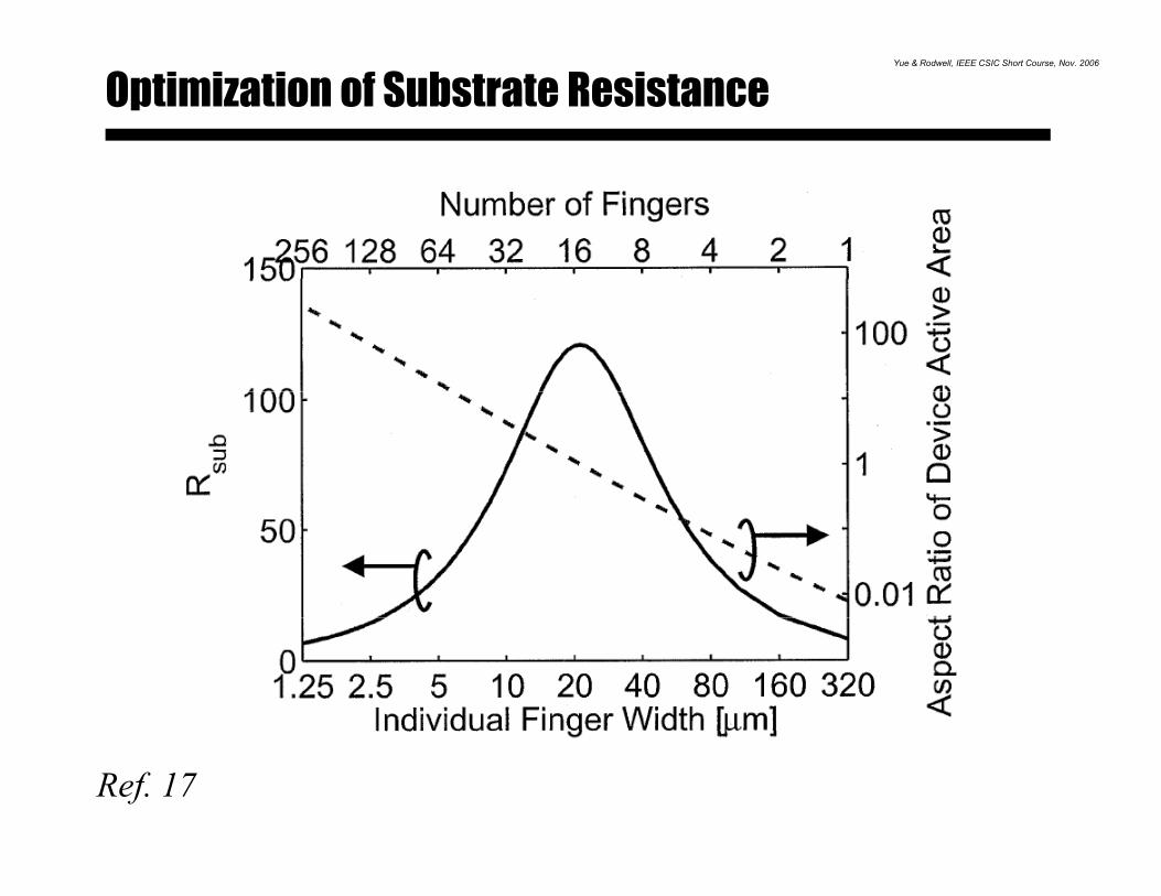
Optimization of Substrate Resistance
Ref. 17

Yue & Rodwell, IEEE CSIC Short Course, Nov. 2006
Interconnect RC Modeling Using 3D Field Solver
SourceGate
Drain
Bottom view showingsubstrate tapsTop view substrate taps
Width (μm) nf Cgs_wire (fF) Cgd_wire (fF) Cds_wire (fF)
2.0 4 2.42 1.61 1.41
• Wire capacitance per finger is extractedp p g

Yue & Rodwell, IEEE CSIC Short Course, Nov. 2006
RF Macro Model vs. Measurement (16 x 2μm/0.12 μm)
15
m]
Core ModelMacro ModelMeasurement
550
575
hm]
18
19
S]
Core ModelMacro ModelMeasurement
5
10
Rin
[Ohm
500
525
550
Rou
t [O
h
Core ModelMacro ModelMeasurement
16
17
18
Gm
[mS
50Core ModelMacro Model 40
Core ModelMacro Model
5 6 7 8 9 100
Frequency [GHz]0 2 4 6 8 10
475
Frequency [GHz]
Measurement
0 2 4 6 8 1015
Frequency [GHz]
15
35
40
45
50
Cin
[fF]
ac o odeMeasurement
30
35
40
Cou
t [fF
]
ac o odeMeasurement
5
10
15
Cfb
[fF]
Core Model
0 2 4 6 8 1030
35
Frequency [GHz]0 2 4 6 8 10
25
Frequency [GHz]0 2 4 6 8 10
0
5
Frequency [GHz]
Macro ModelMeasurement
Rg = 9.8 Ω, Rsub = 475 Ω, Cgs_ext= 4 fF, Cgd_ext= 2.9 fF, Cds_ext= 5.2 fF

Yue & Rodwell, IEEE CSIC Short Course, Nov. 2006
Optimized Layout for fT, fmax and NF
• Parallel Rg improves fmax and NFmin
• Gate connected at both ends• Source drain metals do not overlap• Bulk contacts surround device
Yue & Rodwell, IEEE CSIC Short Course, Nov. 2006
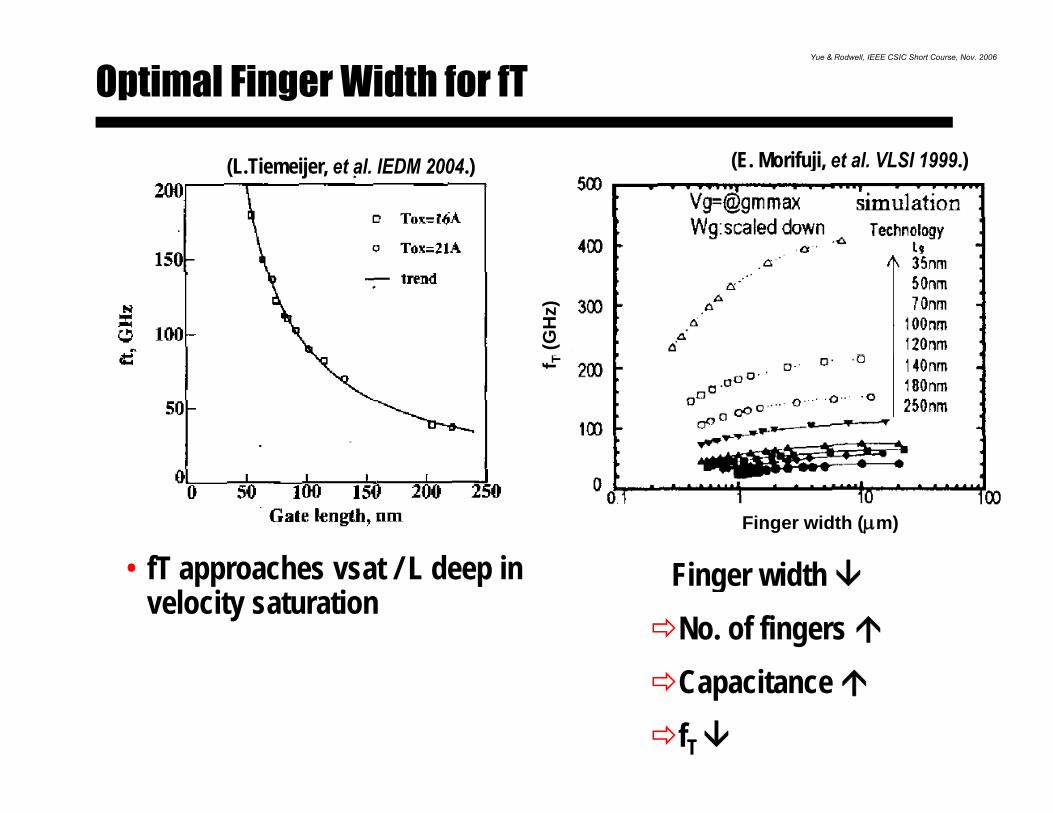
Optimal Finger Width for fT
(E. Morifuji, et al. VLSI 1999.)(L.Tiemeijer, et al. IEDM 2004.)
T(G
Hz)
f TFinger width (μm)
fT h t / L d i Finger width No. of fingers
• fT approaches vsat / L deep in velocity saturation
Capacitance fT

Yue & Rodwell, IEEE CSIC Short Course, Nov. 2006
(E M if ji l VLSI 1999 )
Optimal Finger Width for fmax
(L Ti ij t l IEDM 2004 )(E. Morifuji, et al. VLSI 1999.) (L.Tiemeijer, et al. IEDM 2004.)
f max
(GH
z)
ax(G
Hz)
f
f ma
Finger width (μm) Finger width (μm)
• Reducing Rg vs. increasing Cgg
• For 0.13-μm, optimal finger width is ~2 μm• Optimal finger width decreases with device scaling

Yue & Rodwell, IEEE CSIC Short Course, Nov. 2006
Optimal Finger Width for NF
Finger width (um) Finger width (um)
Noise due to Rg and Rsub can be minimized through layout optimization
Ref. 11

Yue & Rodwell, IEEE CSIC Short Course, Nov. 2006
Optimal Biasing for fT, fMAX and NFMIN
• Peak fT, fMAX and NFMIN characteristic current densities largely unchanged across technology nodes and foundries
• NFMIN (0 15mA/µm) and peak fMAX (0 2mA/µm) are close• NFMIN (0.15mA/µm) and peak fMAX (0.2mA/µm) are closeLNAs simultaneously optimized for noise and high gain
• In CMOS PAs optimum current swing when biased at 0.3mA/µm0.3mA/µm
10% degradation in f
Optimum Current Swing Bias
in fMAX
Bias
Source: Yao, RFIC 2006. - U. of Toronto

Yue & Rodwell, IEEE CSIC Short Course, Nov. 2006
Frequency Response of On-Chip Inductor Q

Yue & Rodwell, IEEE CSIC Short Course, Nov. 2006
First Patterned Ground Shield (PGS)
• Inserted between the inductor and substrate
• PGS fingers connected in ga “star” shape
• Terminates the E fielde ates t e e d• No effect on the H field
I i l ti• Improves isolation

Yue & Rodwell, IEEE CSIC Short Course, Nov. 2006
Self-Shielded Stacked Inductors for high SRF
• Self-shielded layout can effectively boost-strap the overlap capacitance *
• 1-nH inductor can be achieved in 25x25 μm2
using M5 through M8 in a 0 13 μm CMOS 8 metal 25 μm
using M5 through M8 in a 0.13-μm CMOS 8-metal process
* C.-C. Tang, JSSC, April 2002.
Top view
2 l (M7 M8)3 layer (M6-M8)4 layer (M5-M8)
2 layer (M7-M8)
Bottom view

Yue & Rodwell, IEEE CSIC Short Course, Nov. 2006
Systematic mm-wave Design with P-Cells
• Stand-alone single device model is insufficient• Interconnect model accuracy limited by digital RC extraction
• Test structure layout ≠ actual circuit layout
Model Scalability Model Accuracy
Design Flexibility Design Automation
ScalableScalableSubSub--Circuit PCircuit P--CellsCells
Leverage the insight to device layout optimizationLeverage the insight to device layout optimizationExploit the modularity at the sub-circuit level

Yue & Rodwell, IEEE CSIC Short Course, Nov. 2006
Sample P-Cell Layouts and Circuit Models
Diff Pair Cross-Coupled Pair
Cascode
D1 D2
SS
D1 D2G2
D
SS
D1&G2
SS
G1 G2 SG1
D2&G1BB

Yue & Rodwell, IEEE CSIC Short Course, Nov. 2006
Sub-Circuit Cell Library for mm-wave Design
D
G2
D
G2G2D
G2D
Inductor and transformer PCell
G1
S
B
G1
S
B
G2
SG1
G2
SG1
Two transistor sub circuit PCell
5 μm
7 μm 7 μm7 μm
2.71 μm 5 μm
7 μm 7 μm7 μm
2.71 μm
Routing interconnect PCell
Two transistor sub-circuit PCell
Tuned IF Amplifier
Routing interconnect PCell
A unified design and modeling frameworkEach sub circuit P Cell has its scalable circuit modelEach sub-circuit P-Cell has its scalable circuit model

Yue & Rodwell, IEEE CSIC Short Course, Nov. 2006
mm-wave P-Cell Characterization Test Structures
• Measured S-parameters to validate macro models
• UMC 0.13-μm CMOS with 8 copper layers

Yue & Rodwell, IEEE CSIC Short Course, Nov. 2006
Outline
• Background– Emerging mm-wave applications– Open design issues for mm-Wave CMOSOpen design issues for mm Wave CMOS
• CMOS for mm-wave design– Optimizing CMOS device performance – layout & bias
On chip inductors in CMOS– On-chip inductors in CMOS– Cell-based device modeling and design methodology– State of the art CMOS mm-Wave design examples
• mm-Wave design techniques– Device characterization issues – Unconditionally stable, gain-matched amplifier design procedurey , g p g p– Tuned amplifier, power amplifier design examples– On-chip transmission line design
• Summary• Summary• References

Yue & Rodwell, IEEE CSIC Short Course, Nov. 2006
140-220 & 220-330 GHz On-Wafer Network Analysis
• HP8510C VNA, Oleson Microwave Lab mm-wave Extenders
• coplanar wafer probes made by:GGB Industries, Cascade Microtech
•connection via short length of waveguide
GGB W f P b
• Internal bias Tee’s in probes for biasing active devices
GGB Wafer Probes330 GHz available with bias Tees
•measurements to 100 GHz can be in coax.

Yue & Rodwell, IEEE CSIC Short Course, Nov. 2006
Measuring wideband transistors is very hard ! Much harder than measuring amplifiers
High Frequency Device Gain Measurements : Standard Pads
Measuring wideband transistors is very hard ! Much harder than measuring amplifiers. Determining fmax in particular is extremely difficult on high-fmax or small devices
Standard "short pads"must strip pad capacitancemust strip pad inductance--or ft will be too high !cal can be bad due to substrate coupling
make pads small and shield them from substrate
35 35
make pads small, and shield them from substratecal can be bad due to probe coupling
use small probe pitch, use well-shielded probes
20
25
30
35
dB)
h21
20
25
30
35
(dB)
U
MAG/MSG
5
10
15
20
Gai
ns (d
Ajbe
= 0.6 x 4.3 um2
Ic = 20.6 mA, V
ce = 1.53 V
Je = 8.0 mA/um2, V
cb= 0.6 V
f 450 GH f 490 GH5
10
15
Gai
ns
f = 450 GHz f = 490 GHz
Ajbe
= 0.6 x 4.3 um2
Ic = 20.6 mA, V
ce = 1.53 V
Je = 8.0 mA/um2, V
cb= 0.6 V
k0
109 1010 1011 1012
Frequency (Hz)
ft = 450 GHz, f
max = 490 GHz
0109 1010 1011 1012
Frequency (Hz)
ft
450 GHz, fmax
490 GHz k

Yue & Rodwell, IEEE CSIC Short Course, Nov. 2006
High Frequency Measurements : On-Wafer LRL
Extended Reference planes CPWExtended Reference planestransistors placed at center of long on-wafer lineLRL standards placed on waferlarge probe separation → probe coupling reducedstill should use the best-shielded probes available
CPW
Problem: substrate mode couplingmethod will FAIL if lines couple to substrate modes→ method works very poorly with CPW linesneed on wafer thin-film microstrip linesneed on wafer thin film microstrip lines

Yue & Rodwell, IEEE CSIC Short Course, Nov. 2006
Unilateral Power Gain
1212
GainlUnilaterasMason'isgainpowerResultingoutput andinput Match2)0
feedback lossless external ithfeedback w device Cancel 1)SY ==→
( )12212211
21221
4
GainlUnilateras Masonis gainpower Resulting
GGGGYY
U−−
=
design IC torelevance historical ofmostly U unilateral madeeasily not are amplifiers Monolithic
→ 30U
find toionextrapolatfor useful U dB/decade 20-at off rolls Umodel, BJTsimpleFor
maxf→
15
20
25
AG
, dB
Common emitter
ionextrapolat for use tohard U ninteractio -- frompeak shows U FETs,V-III In
maxfRRC dsds
→5
10
15M
SG
/MA
Common base
Common Collector
Common emitter
ionextrapolat for OK be should U substrateby sheilded is CMOS,bulk For
maxfCds
→0
10 100 1000Frequency, GHz
Yue & Rodwell, IEEE CSIC Short Course, Nov. 2006
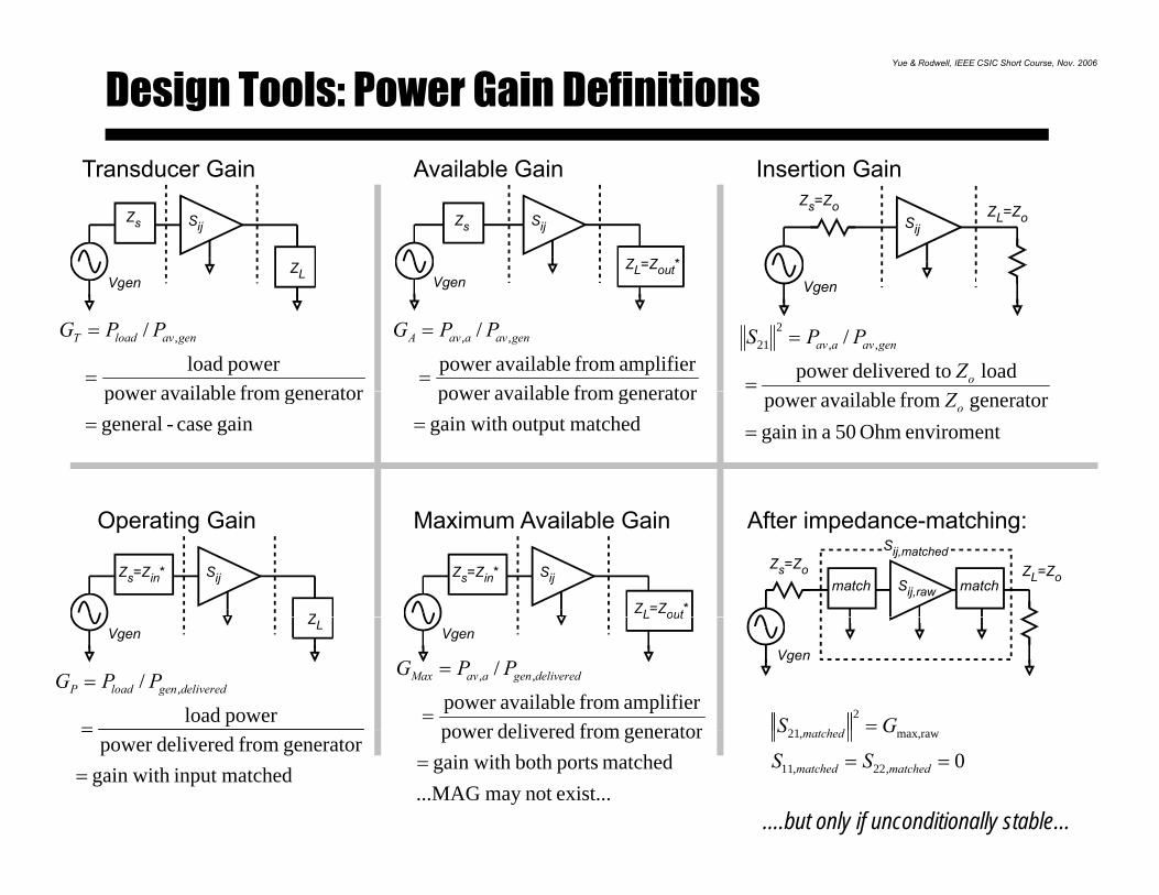
Design Tools: Power Gain Definitions
Transducer Gain Available Gain Insertion GainTransducer Gain
ZL
Zs
V
Sij
Available Gain
Zs
V
Sij
ZL=Zout*
Sij
Zs=Zo ZL=Zo
Insertion Gain
Vgen
generatorfromavailablepowerpower load
/ ,
=
= genavloadT PPG
generatorfromavailablepoweramplifier from availablepower
/ ,,
=
= genavaavA PPG
Vgen Vgen
load todeliveredpower / ,,
221
=
=
o
genavaav
ZPPS
gain case-general generator from availablepower
= matchedoutput withgain generatorfromavailablepower
= enviroment Ohm 50a in gain generatorfromavailablepower
=oZ
Sij,raw
Zs=Zo ZL=Zomatch match
Sij,matched
Zs=Zin* Sij
ZL=Zout*
Operating Gain
Z
Zs=Zin* Sij
Maximum Available Gain After impedance-matching:
VgenVgen
L outZLVgen
power load/ ,
=
= deliveredgenloadP PPG
generatorfromdeliveredpoweramplifier from availablepower
/ ,,
=
= deliveredgenaavMax PPG
221 =h d GS
matchedinput withgain generator from deliveredpower
=
=
exist...not may ...MAG matched ports both withgain
generatorfromdeliveredpower = 0,22,11
rawmax,,21
== matchedmatched
matched
SS
GS
....but only if unconditionally stable...

Yue & Rodwell, IEEE CSIC Short Course, Nov. 2006
Design Tools: Stability Factors, Stability CirclesSSS Γ+Γ 2112 SSS Γ+Γ 2112
S21
S22S11 ΓL
LLin S
SΓ−
Γ+=Γ22
211211 1 S
Sout SS
Γ−Γ+=Γ
11
211222 1
S21
SS22S11
ΓS( )
factorstabilityRolletK:if , all with(stable
stablenally Unconditio
=ΓΓ SL
S122211 L S12
2211
Load Stability Circle Source Stability Circle
[ ]
measurestabilityBand
12
det1
factorstability Rollet K
1221
2222
211
=
>+−−
=
=
SSSSS
[ ] 0det1
measurestability Band22
222
11 >−−−=
=
SSS
inR negative lies beyond 1make which of Values
in
L
→=Γ
Γ
outR negative lies beyond 1make which of Values
out
S
→=Γ
Γ
Negative port impedance→ negative-R oscillatorTuning for highest gain→ infinite gain (oscillation)

Yue & Rodwell, IEEE CSIC Short Course, Nov. 2006
Design Tools: Maximum Stable Gain
SGibli
12
21
12
21
12
21
MSGgain stable Maximum
ZZ
YY
SS
===
= circles at 50 GHz
17 Ω circle
t bili tistabilization methods Sij Sij
Sij Sij
17 Ω
~50 Ω
75 Ω
MSGresults
~5-10 Ω
~75 Ω
MAG 50 GHz
Adding series/shunt resistance excludes source or load from unstable regions → stabilizes

Yue & Rodwell, IEEE CSIC Short Course, Nov. 2006
Design Procedure: Simple Gain-Matched Amplifier
First: stabilize at the design frequency
---device is potentially unstableat 100 GHz design frequencyat 100 GHz design frequency
source stability circle: ~5 Ohm on input willoverstabilize the device
S_S
tabC
ircle
1
After stabilizing(slightly over-stabilizing)

Yue & Rodwell, IEEE CSIC Short Course, Nov. 2006
Design Procedure: Simple Gain-Matched Amplifieravailable gain operating gain
Second: Determine required interface impedances
The Ga & Gp circles define the source & load impedances
g p g g
source & load impedances which the transistor must see
...it is necessary to OVERSTABILIZEth d i t th G & G i l
ΖS,opt ΖL,opt
the device to move the Ga & Gp circles towards the Smith chart center
Thi d dd d t d i th lifi i t tThird: Design Input & Output Tuning Networks ...to provide these impedances...
...added to device, the amplifier is not yet complete...

Yue & Rodwell, IEEE CSIC Short Course, Nov. 2006
Design Procedure: Simple Gain-Matched Amplifiersource & load stability circles & 10,20,...,100 GHzsource & load stability circles & 10,20,...,100 GHz
Forth: Add out-of-band stabilizationpotentially unstable below 75 GHz
with frequency-selectiveseries stabilization
...caused only slight mistuning& slight gain drop @ 100 GHz& slight gain drop @ 100 GHz
...and is unconditionallyt bl b 10 GHstable above 10 GHz

Yue & Rodwell, IEEE CSIC Short Course, Nov. 2006
Design Procedure: Effect of Line Losses
Finally: adjusting for line losses
high line skin effect losses → reduced gain
but line losses also increase stability factor
loss in gain are partly recoveredb d i t bili ti i t &by reducing stabilization resistance &re-tuning the design
--no analytical procedure; just component tweaking
line losses
line losses have severe impacti VLSI i i i t...in VLSI wiring environment
...particularly at 50 + GHz
...particularly with high-power amplifiers

Yue & Rodwell, IEEE CSIC Short Course, Nov. 2006
20
Tuned Amplifier Examples
-10-505
10153-stage cascode in 180 nm CMOS
-20-15
30 35 40 45 50
8
-2
0
2
4
6
S21
, dB
III-V HBT small-signal amplifiers
-4
2
140 150 160 170 180 190 200 210 220Frequency, GHz
0
10
B
-30
-20
-10
140 150 160 170 180 190 200 210 220
gain
, dB
Frequency (GHz)
Note: simple gain-tuned amplifiers → limited applicationsTransmitters need power amplifiers: need output loadline-match, not gain-matchReceivers need low-noise amplifiers: need input noise-match, not gain-match

Yue & Rodwell, IEEE CSIC Short Course, Nov. 2006
Power Amplifier Design (Cripps method)100
40
60
80
100
rren
t, m
A
breakdown
200 mW
( )( ) maxminmaxmax 81 IVVP −=For maximum saturated output power, & maximum efficiencydevice intrinsic output must see optimum loadline set by:
breakdown maximum current maximum power density
0
20
40
0 1 2 3 4 5 6 7 8
Cu
100 mW
breakdown, maximum current, maximum power density.
parasitic C's and R's representedby external elements...
Vce
or Vds
(V)
ammeter monitors intrinsic junction currentwithout includingcapacitive currents
...(Vcollector-Vemitter )...(Vcollector Vemitter )measures voltageinternal to series parasitic resistances...

Yue & Rodwell, IEEE CSIC Short Course, Nov. 2006
Power Amplifier Design (Cripps Method)
Design steps are 1) input stabilization (in-band)2) output tuning for correct load-line3) input tuning (match)4) out-of-band stabilization
Example: 60 GHz, 30 mW PA, 130 nm BiCMOS

Yue & Rodwell, IEEE CSIC Short Course, Nov. 2006
Design: Multi-Finger Power Amplifiers: Even-mode method
Even-mode equivalent circuit
M l i fi lifi d Wilki bi li l-- Most multi-finger amplifiers do not use Wilkinson combiners: lines are too longEven-mode equivalent circuit maps combined design into single-device designFinal design tuning (E&M simulation) with full circuit model
This method explicitly models all feed parasitics in a large multi-finger transistorMUCH more reliable than using single lumped model for multi-finger device
Yue & Rodwell, IEEE CSIC Short Course, Nov. 2006
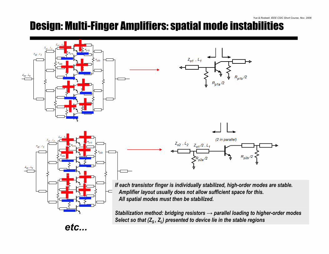
Design: Multi-Finger Amplifiers: spatial mode instabilities
If each transistor finger is individually stabilized, high-order modes are stable.Amplifier layout usually does not allow sufficient space for this.All spatial modes must then be stabilized.
Stabilization method: bridging resistors → parallel loading to higher-order modesSelect so that (ZS , ZL) presented to device lie in the stable regions
etc...

Yue & Rodwell, IEEE CSIC Short Course, Nov. 2006
Design: Multi-Finger Amplifiers: Layout Examples
W-band InP HBT power amplifier - UCSB
mm-wave InP HBT power amplifier - Rockwell
mm-wave InP HBT power amplifier - Rockwell

Yue & Rodwell, IEEE CSIC Short Course, Nov. 2006
Low-Noise Amplifier Design-- device model
Zi ldVd lB i S
)/( 4
)/( 4Zielder Van :model Basic
2,
2,
=
=
HzVkTRS
HzVkTRS
iRVV
gRVV
i
g
CgdRg
Ri
gmVg’s’ GdsG
D
SVV,Rg
SVV,Ri
Sii,channel
mobilityconstantchannellong:2/3
)/( 4
)/( 42
,
2,
⎧
Γ=
=
HzAgkTS
HzVkTRS
mchannelII
sRVV s
i
Cgs Vg’s’
Rs
Cdb
MTT)TransIEEEHughes(B neglected be can densities-spectral Cross
field highunder 2/3
mobilityconstant channel, long :2/3
⎩⎨⎧>
=Γ
S
Csb
SVV,Rs
MTT)Trans IEEE Hughes,(B.
CgdRin gmxVg’s’ Gdsx
G
D
SVV,RinSii,channel
HVkTRS )/(4model noise Simplified
2
Cgsx Vg’s’
D
Cdb
→Γ→Γ
=
=
sm
mchannelII
inRVV
RggkTΓS
HzVkTRSin
0 as ' '4
)/( 4
,
2,
S
Csb∞→→Γ smRg as 1'

Yue & Rodwell, IEEE CSIC Short Course, Nov. 2006
Low-Noise Amplifier Design-- sketch of steps in Fmin calculation
:densitiesspectalcurrent & voltagenoiseinput Total
( )( )
( ) )/( 24)(
)/( 2144)(
pgp
22
222
HzAfCgkTfS
HzVRfCgkTkTRfS
gsm
I
ingsm
inE
n
n
Γ=
+Γ
+=
π
π
( )( ) )/( 2214)( * HzAVfCjRfCjgkTfS gsings
mIE nn
×+Γ
= ππ
Zs( )SZSZS R2
:impedance source particulara withfigure Noise*2
Vgen( )
( )s
IEsIsE
ZkTSZSZS
F nnnn
Re4Re2
1⋅++
+=
Z =ZZopt
[ ]( ) [ ]
[ ] [ ]nnnnnn
IEIEE
IEIEIE
SSS
SSSSkT
F
ImIm
Re2Im24
11
figure noise Minimum
2
2min
⎟⎞
⎜⎛
⎥⎦⎤
⎢⎣⎡ +−+=
Vgen
Zs Zonoisematch
[ ] [ ]n
nn
n
nn
n
n
I
IE
I
IE
I
Eoptoptopt S
jSS
jXRZ −⎟⎟⎠
⎜⎜⎝
−=+=
lf(rough) n ExpressioFukui
⎟⎞
⎜⎛
→
gssignalsignalmx
igsopt
signalmigs
Cfjff
gRRR
Z
ff
gRRRF
πτ
τ
21~
)(21~min
+⎟⎟⎠
⎞⎜⎜⎝
⎛⋅
Γ++
⎟⎟⎠
⎞⎜⎜⎝
⎛⋅++Γ+

Yue & Rodwell, IEEE CSIC Short Course, Nov. 2006
Low-Noise Amplifier Design
Zs=Zonoisematch
ZsDesign steps are 1) output stabilization (in-band)2) input tuning for Fmin3) output tuning (match)
Vgen4) out-of-band stabilization
Discrepancy in input noise-match & gain-matchcan be reduced by adding source inductance (R. Van Tuyl)
Example: 60 GHz, LNA, 130 nm BiCMOS
gain & noise circles after input matchingnote compromise between gain & noise tune

Yue & Rodwell, IEEE CSIC Short Course, Nov. 2006
III-V MIMIC Interconnects -- Classic Substrate MicrostripW Zero ground Brass carrier and IC with backside
H
Thick Substrate→ low skin loss
1
Zero ground inductance in package
Brass carrier andassembly ground
interconnectsubstrate
IC with backsideground plane & vias
No ground planebreaks in IC
kz
H Hr
skin 2/11
εα ∝
near-zeroground-groundinductance
IC viaseliminateon-wafergroundloops
High via TM substrate
breaks in IC
High via inductance mode coupling
Strong coupling when substrate approaches ~λd / 4 thickness12 pH for 100 μm substrate -- 7.5 Ω @ 100 GHz
lines must be widely spaced
ground vias must be widely spaced
Line spacings must be ~3*(substrate thickness) all factors require very thin substrates for >100 GHz ICs→ lapping to ~50 μm substrate thickness typical for 100+ GHz
Yue & Rodwell, IEEE CSIC Short Course, Nov. 2006
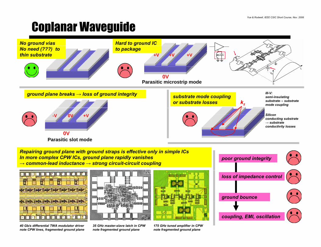
Coplanar WaveguideNo ground vias Hard to ground IC gNo need (???) to thin substrate +V +V +V
0V
gto package
kz
Parasitic microstrip mode0V
substrate mode coupling or substrate losses
ground plane breaks → loss of ground integrity III-V:semi-insulating substrate→ substrate mode coupling
Parasitic slot mode
-V 0V +V
0V
Siliconconducting substrate→ substrate conductivity losses
Parasitic slot mode
Repairing ground plane with ground straps is effective only in simple ICsIn more complex CPW ICs, ground plane rapidly vanishes → common-lead inductance → strong circuit-circuit coupling
poor ground integrity
loss of impedance control
ground bounce
40 Gb/s differential TWA modulator drivernote CPW lines, fragmented ground plane
35 GHz master-slave latch in CPWnote fragmented ground plane
175 GHz tuned amplifier in CPWnote fragmented ground plane
coupling, EMI, oscillation
Yue & Rodwell, IEEE CSIC Short Course, Nov. 2006
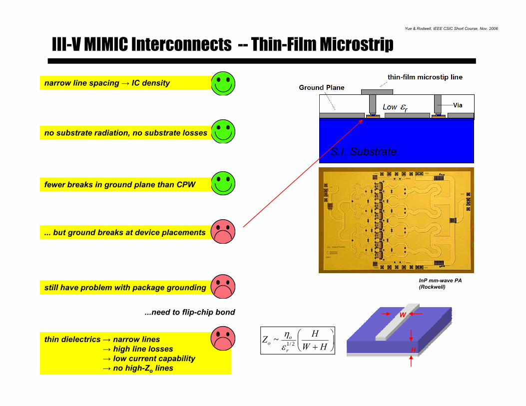
III-V MIMIC Interconnects -- Thin-Film Microstrip
narrow line spacing → IC density
no substrate radiation, no substrate losses
fewer breaks in ground plane than CPW
... but ground breaks at device placements
InP mm wave PAstill have problem with package grounding
W
⎞⎛ H
...need to flip-chip bond
InP mm-wave PA (Rockwell)
thin dielectrics → narrow lines→ high line losses→ low current capability→ no high-Zo lines
H ⎟⎠⎞
⎜⎝⎛
+ HWHZ
r
oo 2/1~
εη
Yue & Rodwell, IEEE CSIC Short Course, Nov. 2006
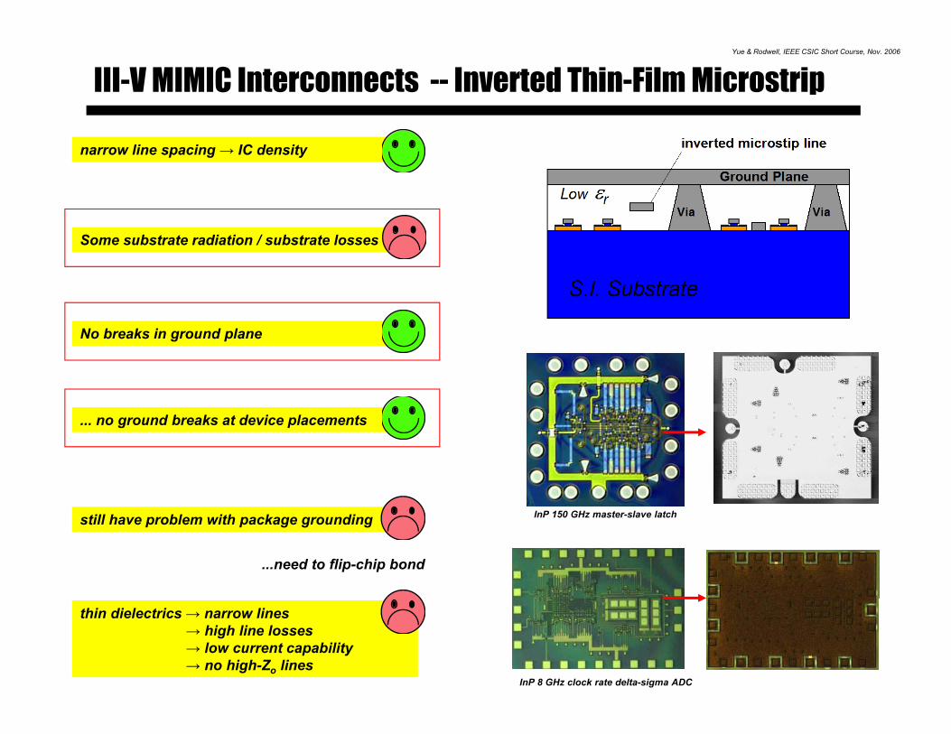
III-V MIMIC Interconnects -- Inverted Thin-Film Microstrip
narrow line spacing → IC density
Some substrate radiation / substrate losses
No breaks in ground plane
... no ground breaks at device placements
still have problem with package grounding
...need to flip-chip bond
InP 150 GHz master-slave latch
thin dielectrics → narrow lines→ high line losses→ low current capability→ no high-Zo lines
InP 8 GHz clock rate delta-sigma ADC

Yue & Rodwell, IEEE CSIC Short Course, Nov. 2006
If It Has Breaks, It Is Not A Ground Plane !
signal line
signal line
line 1
“ground”“ground”
signal line
ground plane
line 2
common-lead inductance
coupling / EMI due to poor ground system integrity is common in high-frequency systemswhether on PC boards...or on ICs.

Yue & Rodwell, IEEE CSIC Short Course, Nov. 2006
No clean ground return ? → interconnects can't be modeled !
35 GHz static dividerinterconnects have no clear local ground returninterconnect inductance is non-localinterconnect inductance has no compact modelinterconnect inductance has no compact model
8 GH l k t d lt i ADC8 GHz clock-rate delta-sigma ADCthin-film microstrip wiringevery interconnect can be modeled as microstripsome interconnects are terminated in their Zosome interconnects are not terminated...but ALL are precisely modeled...but ALL are precisely modeled
InP 8 GHz clock rate delta-sigma ADC

Yue & Rodwell, IEEE CSIC Short Course, Nov. 2006
VLSI mm-Wave Interconnects with Ground Integrity
narrow line spacing → IC density
no substrate radiation, no substrate losses
negligible breaks in ground plane
negligible ground breaks @ device placements
still have problem with package grounding
...need to flip-chip bond
thin dielectrics → narrow lines→ high line losses→ low current capability→ no high-Zo lines

Yue & Rodwell, IEEE CSIC Short Course, Nov. 2006
Example: 150 GHz Master-Slave LatchD i T h lDevice Technology:500 nm InP HBT
Interconnects : inverted thin-film microstrip
Design:All lines modeled as microstrip linesAll lines modeled as microstrip linesrepresentative lines simulated in Agilent / Momentumfit to simple lossy line model (loss, Zo, velocity)
0
10
20
er (d
Bm
)
-20
-10
0
mum
inpu
t pow
e
-40
-30
0 20 40 60 80 100 120 140 160
Min
i
frequency (GHz)

Yue & Rodwell, IEEE CSIC Short Course, Nov. 2006
Example: 20 GHz DDFS Design (Rockwell)designs in progress: MJ Choedesigns in progress: MJ Choe
design target:20 GHz clock rate
circuit topology:ECLECL
device technology:350 GHz (500 nm) InP HBT (Rockwell)
Interconnect technology:gyinverted thin-film microstrip throughout→ all lines are controlled-impedance
shorter lines:unterminated, but modeled,
longer lines:modeled and terminated

Yue & Rodwell, IEEE CSIC Short Course, Nov. 2006
Summary
• At 90-nm or below, CMOS can be a cost-effective choice for highly integrated mm-wave circuits
• Consideration for optimizing device layout and biasing are • Consideration for optimizing device layout and biasing are very similar for mm-wave and RF
• Pre-characterized cell-based mm-wave design flow will be a e c a acte ed ce based a e des g o be akey enabler

Yue & Rodwell, IEEE CSIC Short Course, Nov. 2006
References on other mm-Wave CMOS Efforts
P f B B d d P f A Nik j d “D i id ti f 60 GH • Prof. B. Brodersen and Prof. A. Niknejad – “Design considerations for 60 GHz CMOS radios,” IEEE Communications Magazine, Dec. 2004.
• Prof A Hajimiri – “A fully integrated 24-GHz phased-array transmitter in Prof. A. Hajimiri – A fully integrated 24-GHz phased-array transmitter in CMOS,” IEEE JSSC, Dec. 2005.
• Prof. B. Razavi – “A 60-GHz CMOS receiver front-end” IEEE JSSC, Jan. 2006.• Prof. F. Chang – “A 60GHz CMOS VCO using on-chip resonator with embedded
artificial dielectric for size, loss, and noise reduction,” 2006 ISSCC.• Prof. J. Laskar – “60-GHz direct-conversion gigabit modulator/demodulator on
li id t l l ” IEEE TMTT M 2006liquid-crystal polymer,” IEEE TMTT, Mar. 2006.

Yue & Rodwell, IEEE CSIC Short Course, Nov. 2006
In caseIn casef tiof questionsq