Embed Size (px)
Citation preview
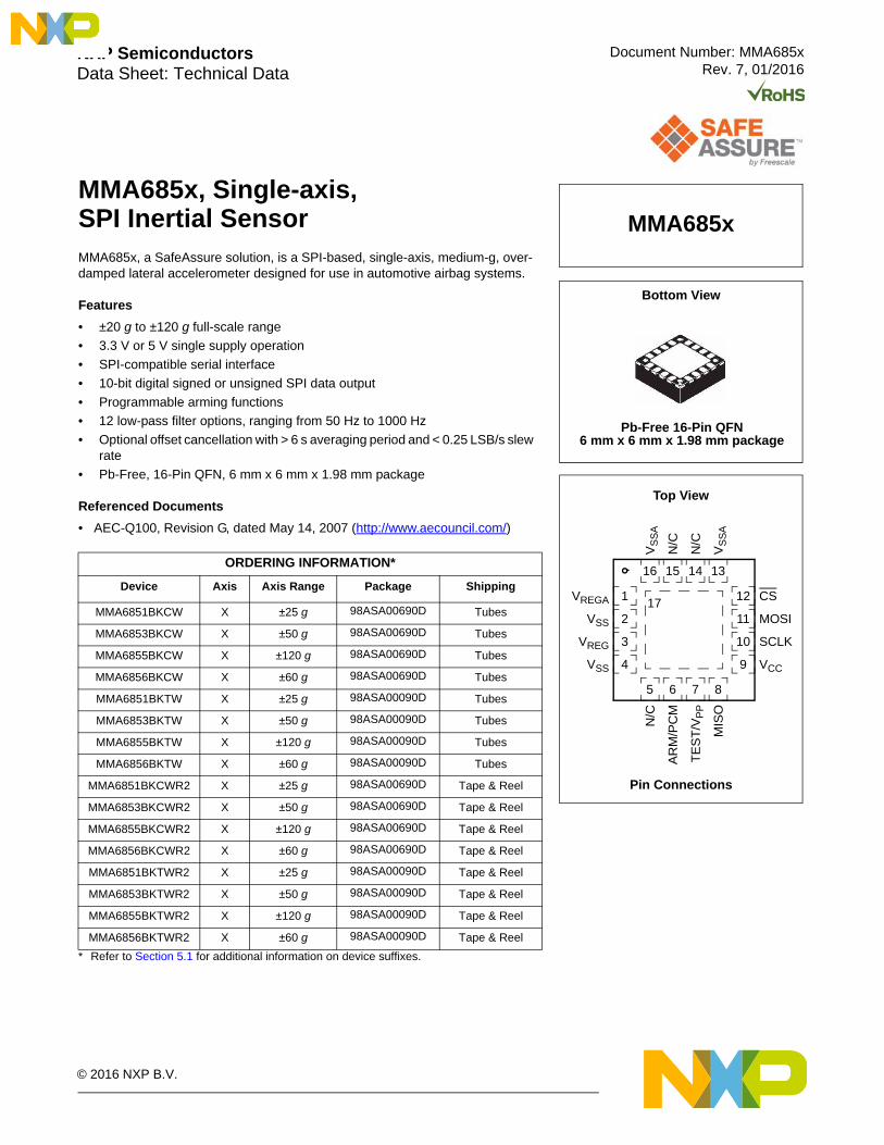
Document Number: MMA685xRev. 7, 01/2016
NXP SemiconductorsData Sheet: Technical Data
MMA685x, Single-axis,SPI Inertial SensorMMA685x, a SafeAssure solution, is a SPI-based, single-axis, medium-g, over-damped lateral accelerometer designed for use in automotive airbag systems.
Features
• ±20 g to ±120 g full-scale range
• 3.3 V or 5 V single supply operation
• SPI-compatible serial interface
• 10-bit digital signed or unsigned SPI data output
• Programmable arming functions
• 12 low-pass filter options, ranging from 50 Hz to 1000 Hz
• Optional offset cancellation with > 6 s averaging period and < 0.25 LSB/s slew rate
• Pb-Free, 16-Pin QFN, 6 mm x 6 mm x 1.98 mm package
Referenced Documents
• AEC-Q100, Revision G, dated May 14, 2007 (http://www.aecouncil.com/)
* Refer to Section 5.1 for additional information on device suffixes.
ORDERING INFORMATION*
Device Axis Axis Range Package Shipping
MMA6851BKCW X ±25 g 98ASA00690D Tubes
MMA6853BKCW X ±50 g 98ASA00690D Tubes
MMA6855BKCW X ±120 g 98ASA00690D Tubes
MMA6856BKCW X ±60 g 98ASA00690D Tubes
MMA6851BKTW X ±25 g 98ASA00090D Tubes
MMA6853BKTW X ±50 g 98ASA00090D Tubes
MMA6855BKTW X ±120 g 98ASA00090D Tubes
MMA6856BKTW X ±60 g 98ASA00090D Tubes
MMA6851BKCWR2 X ±25 g 98ASA00690D Tape & Reel
MMA6853BKCWR2 X ±50 g 98ASA00690D Tape & Reel
MMA6855BKCWR2 X ±120 g 98ASA00690D Tape & Reel
MMA6856BKCWR2 X ±60 g 98ASA00690D Tape & Reel
MMA6851BKTWR2 X ±25 g 98ASA00090D Tape & Reel
MMA6853BKTWR2 X ±50 g 98ASA00090D Tape & Reel
MMA6855BKTWR2 X ±120 g 98ASA00090D Tape & Reel
MMA6856BKTWR2 X ±60 g 98ASA00090D Tape & Reel
Pin Connections
Bottom View
Top View
VREGA
VSSN
/C
VS
SA
N/C
VS
SA
TE
ST
/VP
P
MIS
O
MOSI
SCLK
VCC
VSS
VREG
AR
M/P
CM
1
2
3
4
5 6 7 8
12
11
10
9
16 15 14 13
CS
N/C
17
MMA685x
Pb-Free 16-Pin QFN6 mm x 6 mm x 1.98 mm package
© 2016 NXP B.V.
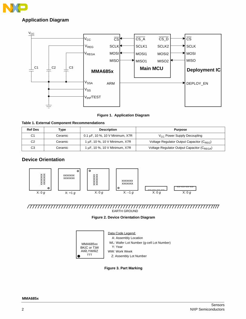
Application Diagram
Figure 1. Application Diagram
Device Orientation
Figure 2. Device Orientation Diagram
Figure 3. Part Marking
Table 1. External Component Recommendations
Ref Des Type Description Purpose
C1 Ceramic 0.1 μF, 10 %, 10 V Minimum, X7R VCC Power Supply Decoupling
C2 Ceramic 1 μF, 10 %, 10 V Minimum, X7R Voltage Regulator Output Capacitor (CREG)
C3 Ceramic 1 μF, 10 %, 10 V Minimum, X7R Voltage Regulator Output Capacitor (CREGA)
C3C1 C2
VCC
MMA685x
VCC
VREG
VREGA
VSS
VPP/TEST
CS
SCLK
ARM
CS_A
SCLK1
MOSI1
Main MCU
MISO1
CS_D
SCLK2
MOSI2
MISO2
CS
SCLK
MOSI
MISO
Deployment IC
DEPLOY_ENVSSA
MOSI
MISO
X: 0 g
EARTH GROUND
X: +1 g X: 0 g X: –1 g X: 0 g X: 0 g
xxxxxxxxxxxxxx
xxxxxxxxxxxxxx
xxxxxxxxxxxxxx
xxxx
xxx
xxxx
xxx
MMA685xx
AWLYWWZ
Data Code Legend:
A: Assembly Location
WL: Wafer Lot Number (g-cell Lot Number)Y: Year
WW: Work Week
Z: Assembly Lot Number
BK(C or T)W
TTT
Sensors2 NXP Semiconductors
MMA685x
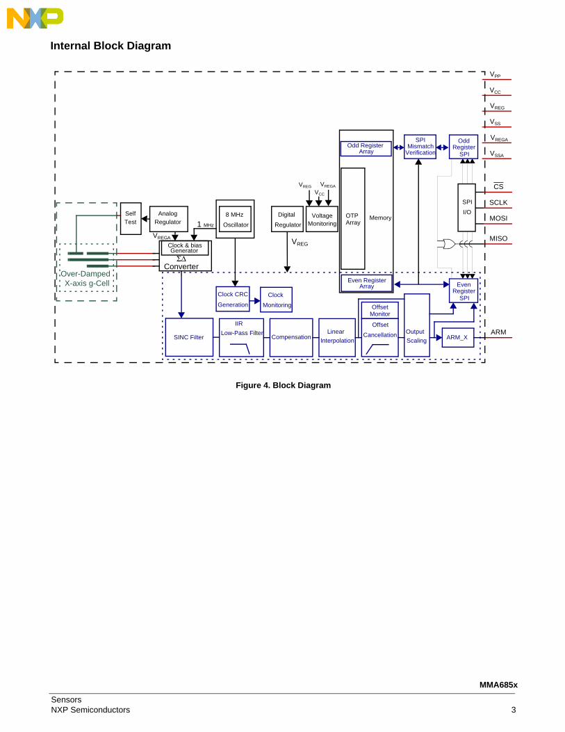
Internal Block Diagram
Figure 4. Block Diagram
ΣΔConverter
Oscillator
8 MHz
1 MHz Regulator
Digital
X-axis g-CellOver-Damped
SINC Filter CompensationLow-Pass Filter Cancellation
Offset
ARM_X
VREGAVREG
Monitoring
Clock
VREGAVREG
VCC
IIR
VPP
VCC
VREG
VSS
VREGA
VSSA
ARM
CS
SCLK
MOSI
MISO
Odd RegisterArray
Generation
Clock CRC
I/O
SPI
MismatchSPI
Even RegisterArray
Verification
Clock & biasGenerator
SPI
OddRegister
SPI
EvenRegister
OTPArray
MemoryAnalog
RegulatorSelfTest
VoltageMonitoring
Linear
Interpolation
Output
Scaling
OffsetMonitor
SensorsNXP Semiconductors 3
MMA685x
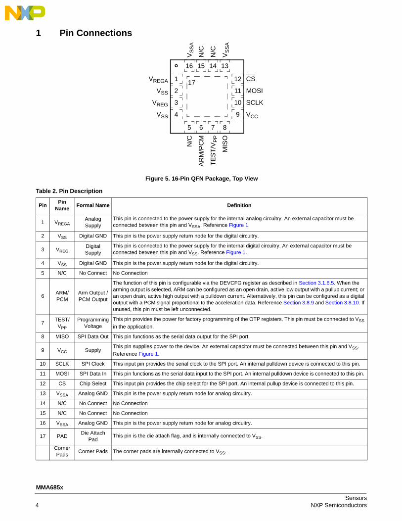
1 Pin Connections
Figure 5. 16-Pin QFN Package, Top View
Table 2. Pin Description
PinPin
NameFormal Name Definition
1 VREGAAnalogSupply
This pin is connected to the power supply for the internal analog circuitry. An external capacitor must be connected between this pin and VSSA. Reference Figure 1.
2 VSS Digital GND This pin is the power supply return node for the digital circuitry.
3 VREGDigitalSupply
This pin is connected to the power supply for the internal digital circuitry. An external capacitor must be connected between this pin and VSS. Reference Figure 1.
4 VSS Digital GND This pin is the power supply return node for the digital circuitry.
5 N/C No Connect No Connection
6ARM/PCM
Arm Output / PCM Output
The function of this pin is configurable via the DEVCFG register as described in Section 3.1.6.5. When the arming output is selected, ARM can be configured as an open drain, active low output with a pullup current; or an open drain, active high output with a pulldown current. Alternatively, this pin can be configured as a digital output with a PCM signal proportional to the acceleration data. Reference Section 3.8.9 and Section 3.8.10. If unused, this pin must be left unconnected.
7TEST/ VPP
Programming Voltage
This pin provides the power for factory programming of the OTP registers. This pin must be connected to VSS
in the application.
8 MISO SPI Data Out This pin functions as the serial data output for the SPI port.
9 VCC SupplyThis pin supplies power to the device. An external capacitor must be connected between this pin and VSS.
Reference Figure 1.
10 SCLK SPI Clock This input pin provides the serial clock to the SPI port. An internal pulldown device is connected to this pin.
11 MOSI SPI Data In This pin functions as the serial data input to the SPI port. An internal pulldown device is connected to this pin.
12 CS Chip Select This input pin provides the chip select for the SPI port. An internal pullup device is connected to this pin.
13 VSSA Analog GND This pin is the power supply return node for analog circuitry.
14 N/C No Connect No Connection
15 N/C No Connect No Connection
16 VSSA Analog GND This pin is the power supply return node for analog circuitry.
17 PADDie Attach
PadThis pin is the die attach flag, and is internally connected to VSS.
Corner Pads
Corner Pads The corner pads are internally connected to VSS.
VREGA
VSS
N/C
VS
SA
N/C
VS
SA
TE
ST
/VP
P
MIS
O
MOSI
SCLK
VCC
VSS
VREG
AR
M/P
CM
1
2
3
4
5 6 7 8
12
11
10
9
16 15 14 13
CS
N/C
17
Sensors4 NXP Semiconductors
MMA685x
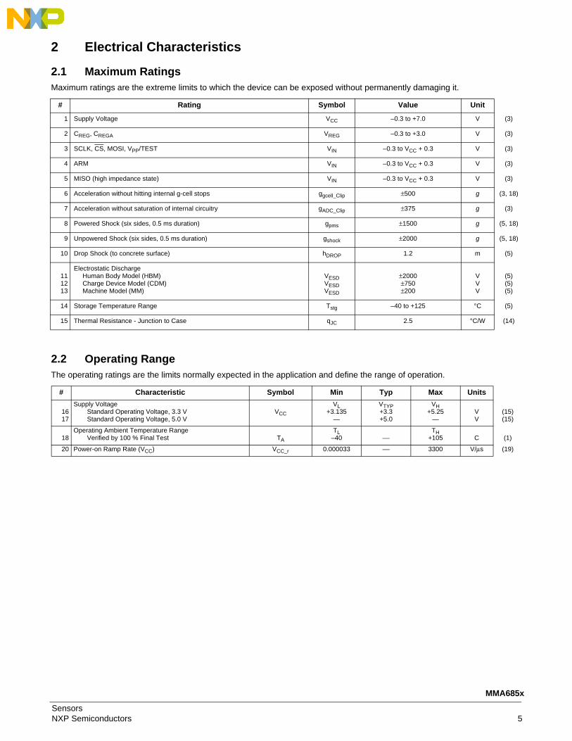
2 Electrical Characteristics
2.1 Maximum RatingsMaximum ratings are the extreme limits to which the device can be exposed without permanently damaging it.
2.2 Operating RangeThe operating ratings are the limits normally expected in the application and define the range of operation.
# Rating Symbol Value Unit
1 Supply Voltage VCC –0.3 to +7.0 V (3)
2 CREG, CREGA VREG –0.3 to +3.0 V (3)
3 SCLK, CS, MOSI, VPP/TEST VIN –0.3 to VCC + 0.3 V (3)
4 ARM VIN –0.3 to VCC + 0.3 V (3)
5 MISO (high impedance state) VIN –0.3 to VCC + 0.3 V (3)
6 Acceleration without hitting internal g-cell stops ggcell_Clip ±500 g (3, 18)
7 Acceleration without saturation of internal circuitry gADC_Clip ±375 g (3)
8 Powered Shock (six sides, 0.5 ms duration) gpms ±1500 g (5, 18)
9 Unpowered Shock (six sides, 0.5 ms duration) gshock ±2000 g (5, 18)
10 Drop Shock (to concrete surface) hDROP 1.2 m (5)
111213
Electrostatic DischargeHuman Body Model (HBM)Charge Device Model (CDM)Machine Model (MM)
VESDVESDVESD
±2000±750±200
VVV
(5)(5)(5)
14 Storage Temperature Range Tstg –40 to +125 °C (5)
15 Thermal Resistance - Junction to Case qJC 2.5 °C/W (14)
# Characteristic Symbol Min Typ Max Units
1617
Supply VoltageStandard Operating Voltage, 3.3 V Standard Operating Voltage, 5.0 V
VCC
VL+3.135
—
VTYP+3.3+5.0
VH+5.25
—VV
(15)(15)
18Operating Ambient Temperature Range
Verified by 100 % Final Test TA
TL–40 ⎯
TH+105 C (1)
20 Power-on Ramp Rate (VCC) VCC_r 0.000033 ⎯ 3300 V/μs (19)
SensorsNXP Semiconductors 5
MMA685x
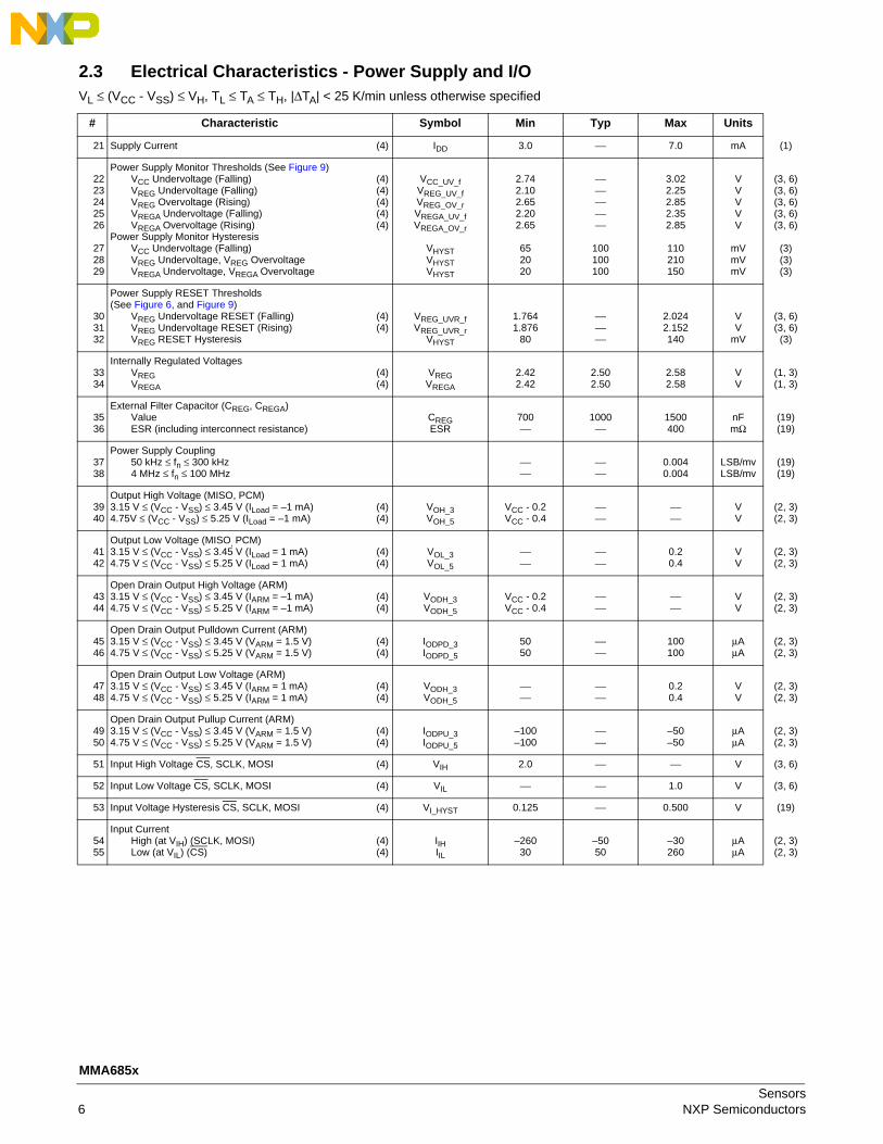
2.3 Electrical Characteristics - Power Supply and I/OVL ≤ (VCC - VSS) ≤ VH, TL ≤ TA ≤ TH, |ΔTA| < 25 K/min unless otherwise specified
# Characteristic Symbol Min Typ Max Units
21 Supply Current (4) IDD 3.0 ⎯ 7.0 mA (1)
2223242526
272829
Power Supply Monitor Thresholds (See Figure 9)VCC Undervoltage (Falling)VREG Undervoltage (Falling)VREG Overvoltage (Rising)VREGA Undervoltage (Falling)VREGA Overvoltage (Rising)
Power Supply Monitor HysteresisVCC Undervoltage (Falling)VREG Undervoltage, VREG OvervoltageVREGA Undervoltage, VREGA Overvoltage
(4)(4)(4)(4)(4)
VCC_UV_fVREG_UV_fVREG_OV_rVREGA_UV_fVREGA_OV_r
VHYSTVHYSTVHYST
2.742.102.652.202.65
652020
⎯⎯⎯⎯⎯
100100100
3.022.252.852.352.85
110210150
VVVVV
mVmVmV
(3, 6)(3, 6)(3, 6)(3, 6)(3, 6)
(3)(3)(3)
303132
Power Supply RESET Thresholds(See Figure 6, and Figure 9)
VREG Undervoltage RESET (Falling)VREG Undervoltage RESET (Rising)VREG RESET Hysteresis
(4)(4)
VREG_UVR_fVREG_UVR_r
VHYST
1.7641.876
80
⎯⎯⎯
2.0242.152140
VV
mV
(3, 6)(3, 6)
(3)
3334
Internally Regulated VoltagesVREGVREGA
(4)(4)
VREGVREGA
2.422.42
2.502.50
2.582.58
VV
(1, 3)(1, 3)
3536
External Filter Capacitor (CREG, CREGA)ValueESR (including interconnect resistance)
CREGESR
700⎯
1000⎯
1500400
nFmΩ
(19)(19)
3738
Power Supply Coupling50 kHz ≤ fn ≤ 300 kHz4 MHz ≤ fn ≤ 100 MHz
⎯⎯
⎯⎯
0.0040.004
LSB/mvLSB/mv
(19)(19)
3940
Output High Voltage (MISO, PCM)3.15 V ≤ (VCC - VSS) ≤ 3.45 V (ILoad = –1 mA)4.75V ≤ (VCC - VSS) ≤ 5.25 V (ILoad = –1 mA)
(4)(4)
VOH_3VOH_5
VCC - 0.2VCC - 0.4
⎯⎯
⎯⎯
VV
(2, 3)(2, 3)
4142
Output Low Voltage (MISO, PCM)3.15 V ≤ (VCC - VSS) ≤ 3.45 V (ILoad = 1 mA)4.75 V ≤ (VCC - VSS) ≤ 5.25 V (ILoad = 1 mA)
(4)(4)
VOL_3VOL_5
⎯⎯
⎯⎯
0.20.4
VV
(2, 3)(2, 3)
4344
Open Drain Output High Voltage (ARM)3.15 V ≤ (VCC - VSS) ≤ 3.45 V (IARM = –1 mA)4.75 V ≤ (VCC - VSS) ≤ 5.25 V (IARM = –1 mA)
(4)(4)
VODH_3VODH_5
VCC - 0.2VCC - 0.4
⎯⎯
⎯⎯
VV
(2, 3)(2, 3)
4546
Open Drain Output Pulldown Current (ARM)3.15 V ≤ (VCC - VSS) ≤ 3.45 V (VARM = 1.5 V)4.75 V ≤ (VCC - VSS) ≤ 5.25 V (VARM = 1.5 V)
(4)(4)
IODPD_3IODPD_5
5050
⎯⎯
100100
μAμA
(2, 3)(2, 3)
4748
Open Drain Output Low Voltage (ARM)3.15 V ≤ (VCC - VSS) ≤ 3.45 V (IARM = 1 mA)4.75 V ≤ (VCC - VSS) ≤ 5.25 V (IARM = 1 mA)
(4)(4)
VODH_3VODH_5
⎯⎯
⎯⎯
0.20.4
VV
(2, 3)(2, 3)
4950
Open Drain Output Pullup Current (ARM)3.15 V ≤ (VCC - VSS) ≤ 3.45 V (VARM = 1.5 V)4.75 V ≤ (VCC - VSS) ≤ 5.25 V (VARM = 1.5 V)
(4)(4)
IODPU_3IODPU_5
–100–100
⎯⎯
–50–50
μAμA
(2, 3)(2, 3)
51 Input High Voltage CS, SCLK, MOSI (4) VIH 2.0 ⎯ ⎯ V (3, 6)
52 Input Low Voltage CS, SCLK, MOSI (4) VIL ⎯ ⎯ 1.0 V (3, 6)
53 Input Voltage Hysteresis CS, SCLK, MOSI (4) VI_HYST 0.125 ⎯ 0.500 V (19)
5455
Input CurrentHigh (at VIH) (SCLK, MOSI)Low (at VIL) (CS)
(4)(4)
IIHIIL
–26030
–5050
–30260
μAμA
(2, 3)(2, 3)
Sensors6 NXP Semiconductors
MMA685x
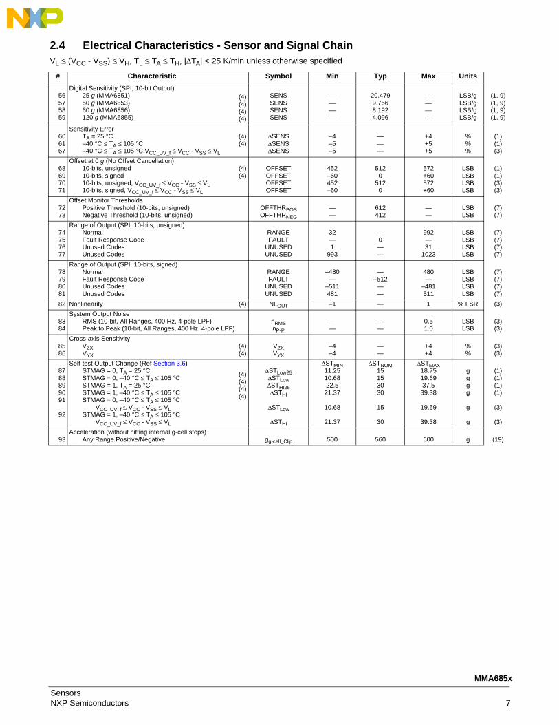
2.4 Electrical Characteristics - Sensor and Signal ChainVL ≤ (VCC - VSS) ≤ VH, TL ≤ TA ≤ TH, |ΔTA| < 25 K/min unless otherwise specified
# Characteristic Symbol Min Typ Max Units
56575859
Digital Sensitivity (SPI, 10-bit Output)25 g (MMA6851)50 g (MMA6853)60 g (MMA6856)120 g (MMA6855)
(4)(4)(4)(4)
SENSSENSSENSSENS
⎯⎯⎯⎯
20.4799.7668.1924.096
⎯⎯⎯⎯
LSB/gLSB/gLSB/gLSB/g
(1, 9)(1, 9)(1, 9)(1, 9)
606167
Sensitivity ErrorTA = 25 °C–40 °C ≤ TA ≤ 105 °C–40 °C ≤ TA ≤ 105 °C,VCC_UV_f ≤ VCC - VSS ≤ VL
(4)(4)
ΔSENSΔSENSΔSENS
–4–5–5
⎯⎯⎯
+4+5+5
%%%
(1)(1)(3)
68697071
Offset at 0 g (No Offset Cancellation)10-bits, unsigned10-bits, signed10-bits, unsigned, VCC_UV_f ≤ VCC - VSS ≤ VL10-bits, signed, VCC_UV_f ≤ VCC - VSS ≤ VL
(4)(4)
OFFSETOFFSETOFFSETOFFSET
452–60452–60
5120
5120
572+60572+60
LSBLSBLSBLSB
(1)(1)(3)(3)
7273
Offset Monitor ThresholdsPositive Threshold (10-bits, unsigned)Negative Threshold (10-bits, unsigned)
OFFTHRPOSOFFTHRNEG
——
612412
——
LSBLSB
(7)(7)
74757677
Range of Output (SPI, 10-bits, unsigned)NormalFault Response CodeUnused CodesUnused Codes
RANGEFAULT
UNUSEDUNUSED
32—1
993
—0——
992—31
1023
LSBLSBLSBLSB
(7)(7)(7)(7)
78798081
Range of Output (SPI, 10-bits, signed)NormalFault Response CodeUnused CodesUnused Codes
RANGEFAULT
UNUSEDUNUSED
–480—
–511481
—–512
——
480—
–481511
LSBLSBLSBLSB
(7)(7)(7)(7)
82 Nonlinearity (4) NLOUT –1 — 1 % FSR (3)
8384
System Output NoiseRMS (10-bit, All Ranges, 400 Hz, 4-pole LPF)Peak to Peak (10-bit, All Ranges, 400 Hz, 4-pole LPF)
nRMSnP-P
——
——
0.51.0
LSBLSB
(3)(3)
8586
Cross-axis SensitivityVZXVYX
(4)(4)
VZXVYX
–4–4
——
+4+4
%%
(3)(3)
8788899091
92
Self-test Output Change (Ref Section 3.6) STMAG = 0, TA = 25 °CSTMAG = 0, –40 °C ≤ TA ≤ 105 °CSTMAG = 1, TA = 25 °CSTMAG = 1, –40 °C ≤ TA ≤ 105 °CSTMAG = 0, –40 °C ≤ TA ≤ 105 °C
VCC_UV_f ≤ VCC - VSS ≤ VLSTMAG = 1, –40 °C ≤ TA ≤ 105 °C
VCC_UV_f ≤ VCC - VSS ≤ VL
(4)(4)(4)(4)
ΔSTLow25ΔSTLowΔSTHI25ΔSTHI
ΔSTLow
ΔSTHI
ΔSTMIN11.2510.6822.521.37
10.68
21.37
ΔSTNOM15153030
15
30
ΔSTMAX18.7519.6937.5
39.38
19.69
39.38
gggg
g
g
(1)(1)(1)(1)
(3)
(3)
93Acceleration (without hitting internal g-cell stops)
Any Range Positive/Negative gg-cell_Clip 500 560 600 g (19)
SensorsNXP Semiconductors 7
MMA685x
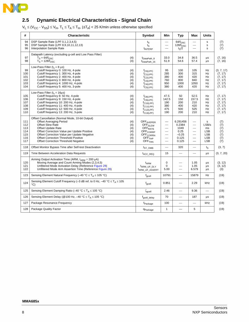
2.5 Dynamic Electrical Characteristics - Signal ChainVL ≤ (VCC - VSS) ≤ VH, TL ≤ TA ≤ TH, |ΔTA| < 25 K/min unless otherwise specified
# Characteristic Symbol Min Typ Max Units
949596
DSP Sample Rate (LPF 0,1,2,3,4,5)DSP Sample Rate (LPF 8,9,10,11,12,13)Interpolation Sample Rate
tStS
tINTERP
⎯⎯⎯
64/fOSC128/fOSC
tS/2
⎯⎯⎯
sss
(7)(7)(7)
9798
Datapath Latency (excluding g-cell and Low Pass Filter)TS = 64/fOSCTS = 128/fOSC
(4)(4)
tDataPath_8tDataPath_16
33.051.9
34.854.6
36.557.4
μsμs
(7, 16)(7, 16)
99100101102103104
Low-Pass Filter (ts = 8 μs)Cutoff frequency 0: 100 Hz, 4-poleCutoff frequency 1: 300 Hz, 4-poleCutoff frequency 2: 400 Hz, 4-poleCutoff frequency 3: 800 Hz, 4-poleCutoff frequency 4: 1000 Hz, 4-poleCutoff frequency 5: 400 Hz, 3-pole
(4)(4)(4)(4)(4)(4)
fC0(LPF)fC1(LPF)fC2(LPF)fC3(LPF)fC4(LPF)fC5(LPF)
95285380760950380
100300400800
1000400
1053154208401050420
HzHzHzHzHzHz
(3, 7, 17)(7, 17)(7, 17)(7, 17)(7, 17)(7, 17)
105106107108109110
Low-Pass Filter (ts = 16μs)Cutoff frequency 8: 50 Hz, 4-poleCutoff frequency 9: 150 Hz, 4-poleCutoff frequency 10: 200 Hz, 4-poleCutoff frequency 11: 400 Hz, 4-poleCutoff frequency 12: 500 Hz, 4-poleCutoff frequency 13: 200 Hz, 3-pole
(4)(4)(4)(4)(4)(4)
fC8(LPF)fC9(LPF)fC10(LPF)fC11(LPF)fC12(LPF)fC13(LPF)
47.5142.5190380475190
50150200400500200
52.5157.5210420525210
HzHzHzHzHzHz
(7, 17)(7, 17)(7, 17)(7, 17)(7, 17)(7, 17)
111112113114115116117
Offset Cancellation (Normal Mode, 10-bit Output)Offset Averaging PeriodOffset Slew RateOffset Update RateOffset Correction Value per Update PositiveOffset Correction Value per Update NegativeOffset Correction Threshold PositiveOffset Correction Threshold Negative
(4)(4)(4)(4)(4)(4)(4)
OFFAVEPEROFFSLEWOFFRATE
OFFCORRPOFFCORRN
OFFTHPOFFTHN
⎯⎯⎯⎯⎯⎯⎯
6.2914560.238410490.25–0.250.1250.125
⎯⎯⎯⎯⎯⎯⎯
sLSB/s
msLSBLSBLSBLSB
(7)(7)(7)(7)(7)(7)(7)
118 Offset Monitor Bypass Time after Self-test Deactivation tST_OMB ⎯ 320 ⎯ tS (3, 7)
119 Time Between Acceleration Data Requests tACC_REQ 15 ⎯ ⎯ μs (3, 7, 20)
120121122
Arming Output Activation Time (ARM, IARM = 200 μA)Moving Average and Count Arming Modes (2,3,4,5)Unfiltered Mode Activation Delay (Reference Figure 29)Unfiltered Mode Arm Assertion Time (Reference Figure 29)
tARMtARM_UF_DLY
tARM_UF_ASSERT
00
5.00
⎯⎯⎯
1.051.056.579
μsμsμs
(3, 12)(3, 12)
(3)
123 Sensing Element Natural Frequency (–40 °C ≤ TA ≤ 105 °C) fgcell 10791 ⎯ 15879 Hz (19)
124Sensing Element Cutoff Frequency (–3 dB ref. to 0 Hz, –40 °C ≤ TA ≤ 105 °C)
fgcell 0.851 ⎯ 2.29 kHz (19)
125 Sensing Element Damping Ratio (–40 °C ≤ TA ≤ 105 °C) ζgcell 2.46 ⎯ 9.36 ⎯ (19)
126 Sensing Element Delay (@100 Hz, –40 °C ≤ TA ≤ 105 °C) fgcell_delay 70 ⎯ 187 μs (19)
127 Package Resonance Frequency fPackage 100 ⎯ ⎯ kHz (19)
128 Package Quality Factor qPackage 1 ⎯ 5 (19)
Sensors8 NXP Semiconductors
MMA685x
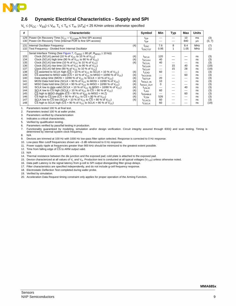
2.6 Dynamic Electrical Characteristics - Supply and SPIVL ≤ (VCC - VSS) ≤ VH, TL ≤ TA ≤ TH, |ΔTA| < 25 K/min unless otherwise specified
1. Parameters tested 100 % at final test.2. Parameters tested 100 % at wafer probe.3. Parameters verified by characterization4. Indicates a critical characteristic.5. Verified by qualification testing.6. Parameters verified by pass/fail testing in production.7. Functionality guaranteed by modeling, simulation and/or design verification. Circuit integrity assured through IDDQ and scan testing. Timing is
determined by internal system clock frequency.8. N/A9. Devices are trimmed at 100 Hz with 1000 Hz low-pass filter option selected. Response is corrected to 0 Hz response.10. Low-pass filter cutoff frequencies shown are –3 dB referenced to 0 Hz response.11. Power supply ripple at frequencies greater than 900 kHz should be minimized to the greatest extent possible.12. Time from falling edge of CS to ARM output valid.13. N/A14. Thermal resistance between the die junction and the exposed pad; cold plate is attached to the exposed pad.15. Device characterized at all values of VL and VH. Production test is conducted at all typical voltages (VTYP) unless otherwise noted.16. Data path Latency is the signal latency from g-cell to SPI output disregarding filter group delays.17. Filter characteristics are specified independently, and do not include g-cell frequency response.18. Electrostatic Deflection Test completed during wafer probe.19. Verified by simulation.20. Acceleration Data Request timing constraint only applies for proper operation of the Arming Function.
# Characteristic Symbol Min Typ Max Units
129130
Power-On Recovery Time (VCC = VCCMIN to first SPI access)Power-On Recovery Time (Internal POR to first SPI access)
tOPtOP
⎯⎯
⎯⎯
10840
msμs
(3)(3, 7)
131132
Internal Oscillator FrequencyTest Frequency - Divided from Internal Oscillator
(4) fOSCfOSCTST
7.60.95
81
8.41.05
MHzMHz
(7)(1)
133134135136137138139140141142143144145146147148
Serial Interface Timing (See Figure 7, CMISO ≤ 80 pF, RMISO ≥ 10 kΩ)Clock (SCLK) period (10 % of VCC to 10 % of VCC)Clock (SCLK) high time (90 % of VCC to 90 % of VCC)Clock (SCLK) low time (10 % of VCC to 10 % of VCC)Clock (SCLK) rise time (10 % of VCC to 90 % of VCC)Clock (SCLK) fall time (90 % of VCC to 10 % of VCC)CS asserted to SCLK high (CS = 10 % of VCC to SCLK = 10 % of VCC)CS asserted to MISO valid (CS = 10 % of VCC to MISO = 10/90 % of VCC)Data setup time (MOSI = 10/90 % of VCC to SCLK = 10 % of VCC)MOSI Data hold time (SCLK = 90 % of VCC to MOSI = 10/90 % of VCC)MISO Data hold time (SCLK = 90 % of VCC to MISO = 10/90 % of VCC)SCLK low to data valid (SCLK = 10 % of VCC to MISO = 10/90 % of VCC)SCLK low to CS high (SCLK = 10 % of VCC to CS = 90 % of VCC)CS high to MISO disable (CS = 90 % of VCC to MISO = Hi Z)CS high to CS low (CS = 90 % of VCC to CS = 90 % of VCC)SCLK low to CS low (SCLK = 10 % of VCC to CS = 90 % of VCC)CS high to SCLK high (CS = 90 % of VCC to SCLK = 90 % of VCC)
(4)(4)(4)
(4)(4)(4)(4)(4)(4)(4)(4)(4)(4)
tSCLKtSCLKHtSCLKLtSCLKRtSCLKFtLEAD
tACCESStSETUP
tHOLD_INtHOLD_OUT
tVALIDtLAG
tDISABLEtCSN
tCLKCStCSCLK
1204040⎯⎯60⎯20100⎯60⎯
5266060
⎯⎯⎯1515⎯⎯⎯⎯⎯⎯⎯⎯⎯⎯⎯
⎯⎯⎯4028⎯60⎯⎯⎯40⎯60⎯⎯⎯
nsnsnsnsnsnsnsnsnsnsnsnsnsnsnsns
(3)(3)(3)(19)(19)(3)(3)(3)(3)(3)(3)(3)(3)(3)(3)(19)
SensorsNXP Semiconductors 9
MMA685x
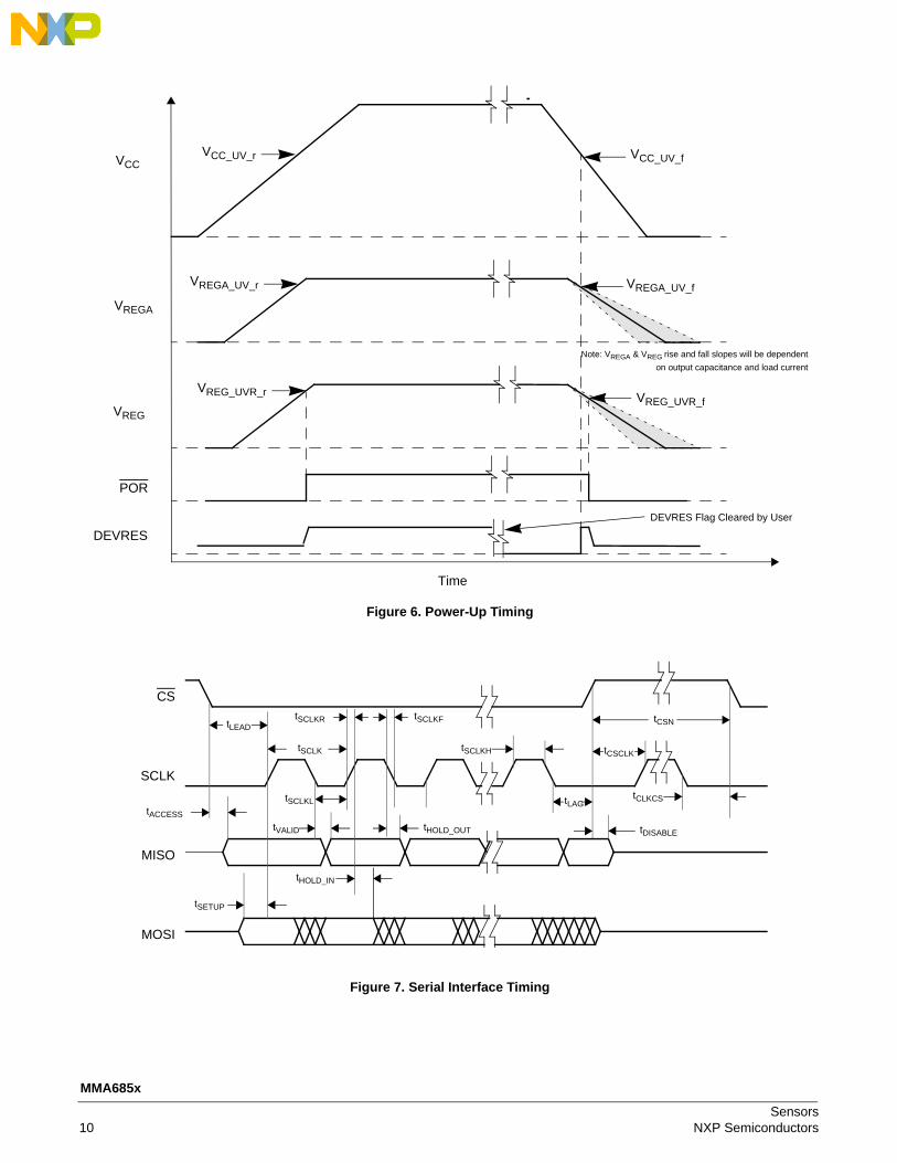
Figure 6. Power-Up Timing
Figure 7. Serial Interface Timing
VCC
POR
VREGA
VREG
DEVRES
VCC_UV_f
VREGA_UV_f
DEVRES Flag Cleared by User
VCC_UV_r
VREGA_UV_r
VREG_UVR_r VREG_UVR_f
Time
Note: VREGA & VREG rise and fall slopes will be dependent
on output capacitance and load current
tSCLK
SCLK
MOSI
CS
MISO
tSCLKH
tSCLKLtACCESS
tSCLKR tSCLKFtLEADtCSN
tSETUP
tHOLD_IN
tVALID tDISABLEtHOLD_OUT
tLAGtCLKCS
tCSCLK
Sensors10 NXP Semiconductors
MMA685x
3 Functional Description
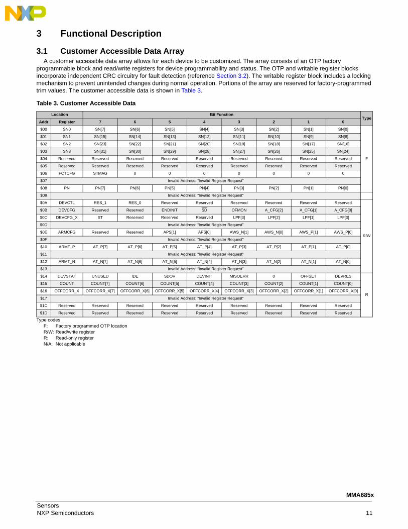
3.1 Customer Accessible Data ArrayA customer accessible data array allows for each device to be customized. The array consists of an OTP factory
programmable block and read/write registers for device programmability and status. The OTP and writable register blocks incorporate independent CRC circuitry for fault detection (reference Section 3.2). The writable register block includes a locking mechanism to prevent unintended changes during normal operation. Portions of the array are reserved for factory-programmed trim values. The customer accessible data is shown in Table 3.
Type codes F: Factory programmed OTP locationR/W: Read/write registerR: Read-only registerN/A: Not applicable
Table 3. Customer Accessible Data
Location Bit FunctionType
Addr Register 7 6 5 4 3 2 1 0
$00 SN0 SN[7] SN[6] SN[5] SN[4] SN[3] SN[2] SN[1] SN[0]
F
$01 SN1 SN[15] SN[14] SN[13] SN[12] SN[11] SN[10] SN[9] SN[8]
$02 SN2 SN[23] SN[22] SN[21] SN[20] SN[19] SN[18] SN[17] SN[16]
$03 SN3 SN[31] SN[30] SN[29] SN[28] SN[27] SN[26] SN[25] SN[24]
$04 Reserved Reserved Reserved Reserved Reserved Reserved Reserved Reserved Reserved
$05 Reserved Reserved Reserved Reserved Reserved Reserved Reserved Reserved Reserved
$06 FCTCFG STMAG 0 0 0 0 0 0 0
$07 Invalid Address: “Invalid Register Request”
$08 PN PN[7] PN[6] PN[5] PN[4] PN[3] PN[2] PN[1] PN[0]
$09 Invalid Address: “Invalid Register Request”
$0A DEVCTL RES_1 RES_0 Reserved Reserved Reserved Reserved Reserved Reserved
R/W
$0B DEVCFG Reserved Reserved ENDINIT SD OFMON A_CFG[2] A_CFG[1] A_CFG[0]
$0C DEVCFG_X ST Reserved Reserved Reserved LPF[3] LPF[2] LPF[1] LPF[0]
$0D Invalid Address: “Invalid Register Request”
$0E ARMCFG Reserved Reserved APS[1] APS[0] AWS_N[1] AWS_N[0] AWS_P[1] AWS_P[0]
$0F Invalid Address: “Invalid Register Request”
$10 ARMT_P AT_P[7] AT_P[6] AT_P[5] AT_P[4] AT_P[3] AT_P[2] AT_P[1] AT_P[0]
$11 Invalid Address: “Invalid Register Request”
$12 ARMT_N AT_N[7] AT_N[6] AT_N[5] AT_N[4] AT_N[3] AT_N[2] AT_N[1] AT_N[0]
$13 Invalid Address: “Invalid Register Request”
$14 DEVSTAT UNUSED IDE SDOV DEVINIT MISOERR 0 OFFSET DEVRES
R
$15 COUNT COUNT[7] COUNT[6] COUNT[5] COUNT[4] COUNT[3] COUNT[2] COUNT[1] COUNT[0]
$16 OFFCORR_X OFFCORR_X[7] OFFCORR_X[6] OFFCORR_X[5] OFFCORR_X[4] OFFCORR_X[3] OFFCORR_X[2] OFFCORR_X[1] OFFCORR_X[0]
$17 Invalid Address: “Invalid Register Request”
$1C Reserved Reserved Reserved Reserved Reserved Reserved Reserved Reserved Reserved
$1D Reserved Reserved Reserved Reserved Reserved Reserved Reserved Reserved Reserved
SensorsNXP Semiconductors 11
MMA685x
3.1.1 Device Serial Number RegistersA unique serial number is programmed into the serial number registers of each MMA685x device during manufacturing. The
serial number is composed of the following information:
Serial numbers begin at 1 for all produced devices in each lot, and are sequentially assigned. Lot numbers begin at 1 and are sequentially assigned. No lot will contain more devices than can be uniquely identified by the 13-bit serial number. Depending on lot size and quantities, all possible lot numbers and serial numbers may not be assigned.
The serial number registers are included in the OTP shadow register array CRC verification. Reference Section 3.2.1 for details regarding the CRC verification. Beyond this, the contents of the serial number registers have no impact on device operation or performance, and are only used for traceability purposes.
3.1.2 Reserved Registers These reserved registers are read-only and have no impact on device operation or performance.
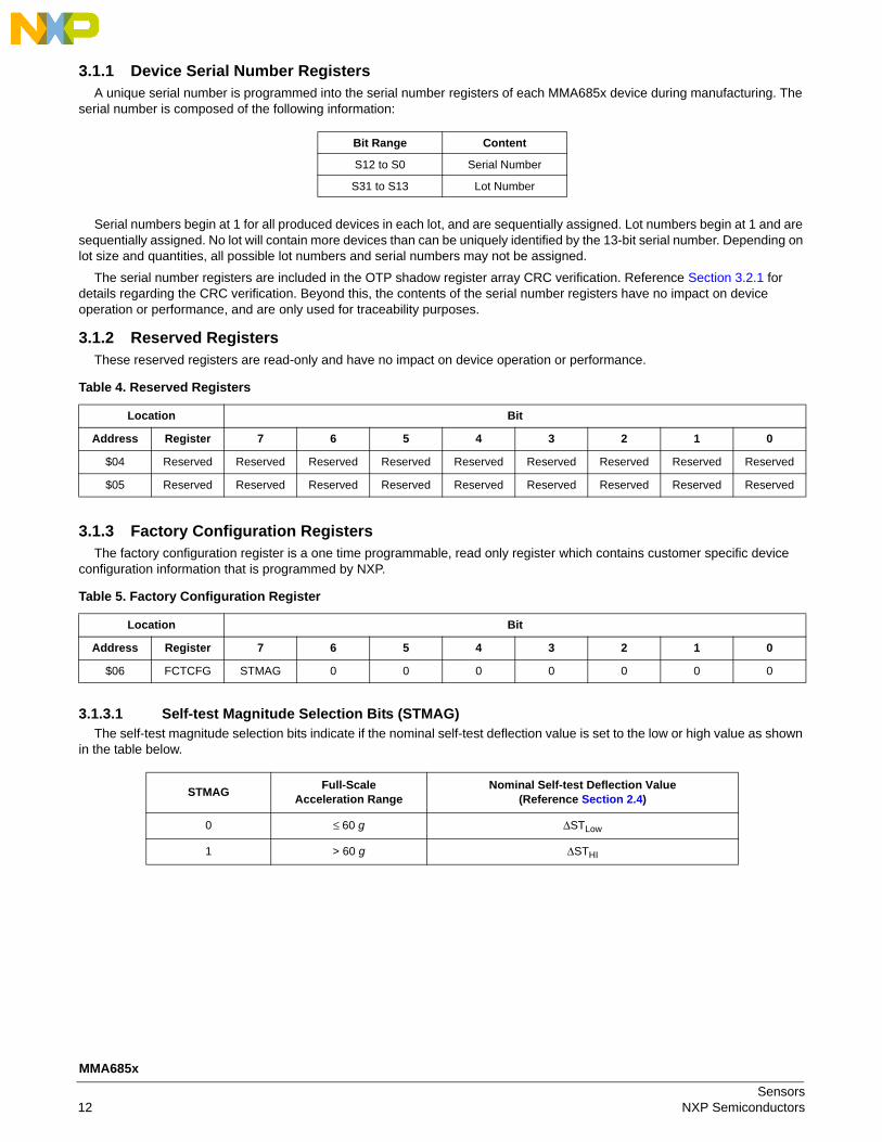
3.1.3 Factory Configuration RegistersThe factory configuration register is a one time programmable, read only register which contains customer specific device
configuration information that is programmed by NXP.
3.1.3.1 Self-test Magnitude Selection Bits (STMAG)The self-test magnitude selection bits indicate if the nominal self-test deflection value is set to the low or high value as shown
in the table below.
Bit Range Content
S12 to S0 Serial Number
S31 to S13 Lot Number
Table 4. Reserved Registers
Location Bit
Address Register 7 6 5 4 3 2 1 0
$04 Reserved Reserved Reserved Reserved Reserved Reserved Reserved Reserved Reserved
$05 Reserved Reserved Reserved Reserved Reserved Reserved Reserved Reserved Reserved
Table 5. Factory Configuration Register
Location Bit
Address Register 7 6 5 4 3 2 1 0
$06 FCTCFG STMAG 0 0 0 0 0 0 0
STMAGFull-Scale
Acceleration RangeNominal Self-test Deflection Value
(Reference Section 2.4)
0 ≤ 60 g ΔSTLow
1 > 60 g ΔSTHI
Sensors12 NXP Semiconductors
MMA685x
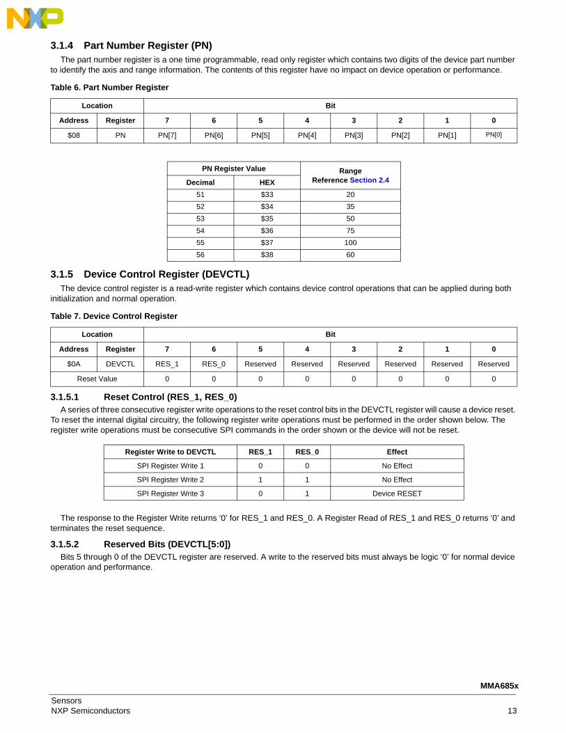
3.1.4 Part Number Register (PN)The part number register is a one time programmable, read only register which contains two digits of the device part number
to identify the axis and range information. The contents of this register have no impact on device operation or performance.
3.1.5 Device Control Register (DEVCTL)The device control register is a read-write register which contains device control operations that can be applied during both
initialization and normal operation.
3.1.5.1 Reset Control (RES_1, RES_0)A series of three consecutive register write operations to the reset control bits in the DEVCTL register will cause a device reset.
To reset the internal digital circuitry, the following register write operations must be performed in the order shown below. The register write operations must be consecutive SPI commands in the order shown or the device will not be reset.
The response to the Register Write returns ‘0’ for RES_1 and RES_0. A Register Read of RES_1 and RES_0 returns ‘0’ and terminates the reset sequence.
3.1.5.2 Reserved Bits (DEVCTL[5:0])Bits 5 through 0 of the DEVCTL register are reserved. A write to the reserved bits must always be logic ‘0’ for normal device
operation and performance.
Table 6. Part Number Register
Location Bit
Address Register 7 6 5 4 3 2 1 0
$08 PN PN[7] PN[6] PN[5] PN[4] PN[3] PN[2] PN[1] PN[0]
PN Register Value RangeReference Section 2.4Decimal HEX
51 $33 20
52 $34 35
53 $35 50
54 $36 75
55 $37 100
56 $38 60
Table 7. Device Control Register
Location Bit
Address Register 7 6 5 4 3 2 1 0
$0A DEVCTL RES_1 RES_0 Reserved Reserved Reserved Reserved Reserved Reserved
Reset Value 0 0 0 0 0 0 0 0
Register Write to DEVCTL RES_1 RES_0 Effect
SPI Register Write 1 0 0 No Effect
SPI Register Write 2 1 1 No Effect
SPI Register Write 3 0 1 Device RESET
SensorsNXP Semiconductors 13
MMA685x
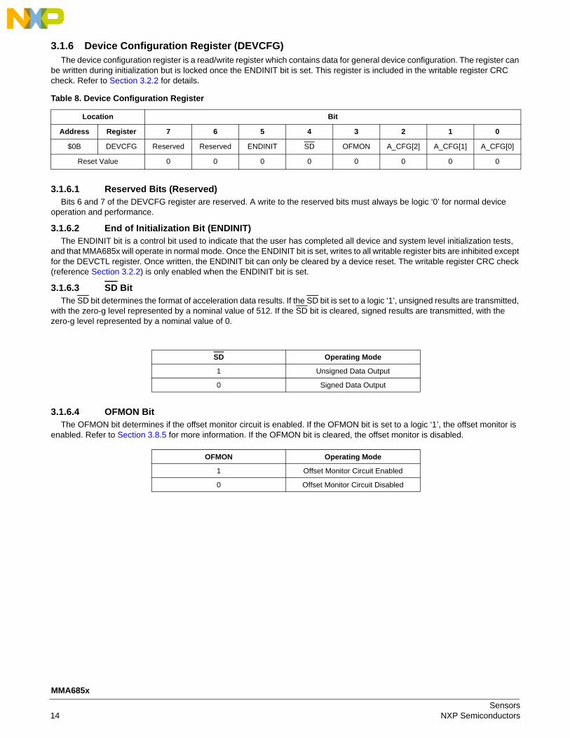
3.1.6 Device Configuration Register (DEVCFG)The device configuration register is a read/write register which contains data for general device configuration. The register can
be written during initialization but is locked once the ENDINIT bit is set. This register is included in the writable register CRC check. Refer to Section 3.2.2 for details.
3.1.6.1 Reserved Bits (Reserved)Bits 6 and 7 of the DEVCFG register are reserved. A write to the reserved bits must always be logic ‘0’ for normal device
operation and performance.
3.1.6.2 End of Initialization Bit (ENDINIT)The ENDINIT bit is a control bit used to indicate that the user has completed all device and system level initialization tests,
and that MMA685x will operate in normal mode. Once the ENDINIT bit is set, writes to all writable register bits are inhibited except for the DEVCTL register. Once written, the ENDINIT bit can only be cleared by a device reset. The writable register CRC check (reference Section 3.2.2) is only enabled when the ENDINIT bit is set.
3.1.6.3 SD BitThe SD bit determines the format of acceleration data results. If the SD bit is set to a logic ‘1’, unsigned results are transmitted,
with the zero-g level represented by a nominal value of 512. If the SD bit is cleared, signed results are transmitted, with the zero-g level represented by a nominal value of 0.
3.1.6.4 OFMON Bit The OFMON bit determines if the offset monitor circuit is enabled. If the OFMON bit is set to a logic ‘1’, the offset monitor is
enabled. Refer to Section 3.8.5 for more information. If the OFMON bit is cleared, the offset monitor is disabled.
Table 8. Device Configuration Register
Location Bit
Address Register 7 6 5 4 3 2 1 0
$0B DEVCFG Reserved Reserved ENDINIT SD OFMON A_CFG[2] A_CFG[1] A_CFG[0]
Reset Value 0 0 0 0 0 0 0 0
SD Operating Mode
1 Unsigned Data Output
0 Signed Data Output
OFMON Operating Mode
1 Offset Monitor Circuit Enabled
0 Offset Monitor Circuit Disabled
Sensors14 NXP Semiconductors
MMA685x
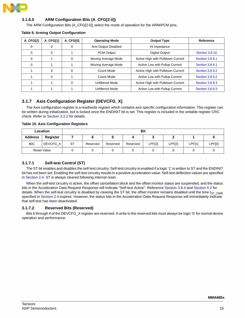
3.1.6.5 ARM Configuration Bits (A_CFG[2:0])The ARM Configuration Bits (A_CFG[2:0]) select the mode of operation for the ARM/PCM pins.
3.1.7 Axis Configuration Register (DEVCFG_X)The Axis configuration register is a read/write register which contains axis specific configuration information. This register can
be written during initialization, but is locked once the ENDINIT bit is set. This register is included in the writable register CRC check. Refer to Section 3.2.2 for details.
3.1.7.1 Self-test Control (ST)The ST bit enables and disables the self-test circuitry. Self-test circuitry is enabled if a logic ‘1’ is written to ST and the ENDINIT
bit has not been set. Enabling the self-test circuitry results in a positive acceleration value. Self-test deflection values are specified in Section 2.4. ST is always cleared following internal reset.
When the self-test circuitry is active, the offset cancellation block and the offset monitor status are suspended, and the status bits in the Acceleration Data Request Response will indicate “Self-test Active”. Reference Section 3.8.4 and Section 4.2 for details. When the self-test circuitry is disabled by clearing the ST bit, the offset monitor remains disabled until the time tST_OMB specified in Section 2.4 expires. However, the status bits in the Acceleration Data Request Response will immediately indicate that self-test has been deactivated.
3.1.7.2 Reserved Bits (Reserved)Bits 6 through 4 of the DEVCFG_X register are reserved. A write to the reserved bits must always be logic ‘0’ for normal device
operation and performance.
Table 9. Arming Output Configuration
A_CFG[2] A_CFG[1] A_CFG[0] Operating Mode Output Type Reference
0 0 0 Arm Output Disabled Hi Impedance
0 0 1 PCM Output Digital Output Section 3.8.10
0 1 0 Moving Average Mode Active High with Pulldown Current Section 3.8.9.1
0 1 1 Moving Average Mode Active Low with Pullup Current Section 3.8.9.1
1 0 0 Count Mode Active High with Pulldown Current Section 3.8.9.2
1 0 1 Count Mode Active Low with Pullup Current Section 3.8.9.2
1 1 0 Unfiltered Mode Active High with Pulldown Current Section 3.8.9.3
1 1 1 Unfiltered Mode Active Low with Pullup Current Section 3.8.9.3
Table 10. Axis Configuration Registers
Location Bit
Address Register 7 6 5 4 3 2 1 0
$0C DEVCFG_X ST Reserved Reserved Reserved LPF[3] LPF[2] LPF[1] LPF[0]
Reset Value 0 0 0 0 0 0 0 0
SensorsNXP Semiconductors 15
MMA685x
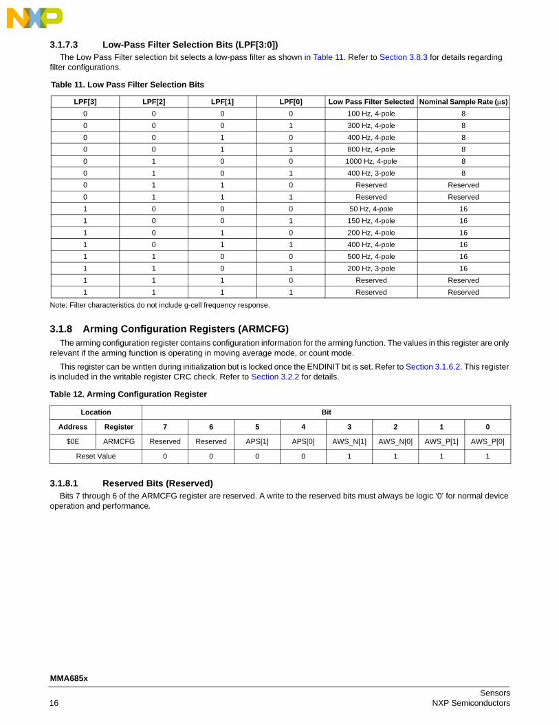
3.1.7.3 Low-Pass Filter Selection Bits (LPF[3:0])The Low Pass Filter selection bit selects a low-pass filter as shown in Table 11. Refer to Section 3.8.3 for details regarding
filter configurations.
Note: Filter characteristics do not include g-cell frequency response.
3.1.8 Arming Configuration Registers (ARMCFG)The arming configuration register contains configuration information for the arming function. The values in this register are only
relevant if the arming function is operating in moving average mode, or count mode.
This register can be written during initialization but is locked once the ENDINIT bit is set. Refer to Section 3.1.6.2. This register is included in the writable register CRC check. Refer to Section 3.2.2 for details.
3.1.8.1 Reserved Bits (Reserved)Bits 7 through 6 of the ARMCFG register are reserved. A write to the reserved bits must always be logic ‘0’ for normal device
operation and performance.
Table 11. Low Pass Filter Selection Bits
LPF[3] LPF[2] LPF[1] LPF[0] Low Pass Filter Selected Nominal Sample Rate (μs)
0 0 0 0 100 Hz, 4-pole 8
0 0 0 1 300 Hz, 4-pole 8
0 0 1 0 400 Hz, 4-pole 8
0 0 1 1 800 Hz, 4-pole 8
0 1 0 0 1000 Hz, 4-pole 8
0 1 0 1 400 Hz, 3-pole 8
0 1 1 0 Reserved Reserved
0 1 1 1 Reserved Reserved
1 0 0 0 50 Hz, 4-pole 16
1 0 0 1 150 Hz, 4-pole 16
1 0 1 0 200 Hz, 4-pole 16
1 0 1 1 400 Hz, 4-pole 16
1 1 0 0 500 Hz, 4-pole 16
1 1 0 1 200 Hz, 3-pole 16
1 1 1 0 Reserved Reserved
1 1 1 1 Reserved Reserved
Table 12. Arming Configuration Register
Location Bit
Address Register 7 6 5 4 3 2 1 0
$0E ARMCFG Reserved Reserved APS[1] APS[0] AWS_N[1] AWS_N[0] AWS_P[1] AWS_P[0]
Reset Value 0 0 0 0 1 1 1 1
Sensors16 NXP Semiconductors
MMA685x
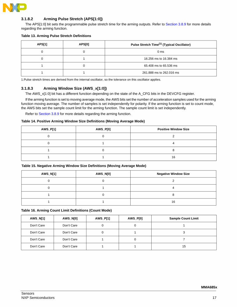
3.1.8.2 Arming Pulse Stretch (APS[1:0])The APS[1:0] bit sets the programmable pulse stretch time for the arming outputs. Refer to Section 3.8.9 for more details
regarding the arming function.
3.1.8.3 Arming Window Size (AWS_x[1:0])The AWS_x[1:0] bit has a different function depending on the state of the A_CFG bits in the DEVCFG register.
If the arming function is set to moving average mode, the AWS bits set the number of acceleration samples used for the arming function moving average. The number of samples is set independently for polarity. If the arming function is set to count mode, the AWS bits set the sample count limit for the arming function. The sample count limit is set independently.
Refer to Section 3.8.9 for more details regarding the arming function.
Table 13. Arming Pulse Stretch Definitions
APS[1] APS[0] Pulse Stretch Time(1) (Typical Oscillator)
1.Pulse stretch times are derived from the internal oscillator, so the tolerance on this oscillator applies.
0 0 0 ms
0 1 16.256 ms to 16.384 ms
1 0 65.408 ms to 65.536 ms
1 1 261.888 ms to 262.016 ms
Table 14. Positive Arming Window Size Definitions (Moving Average Mode)
AWS_P[1] AWS_P[0] Positive Window Size
0 0 2
0 1 4
1 0 8
1 1 16
Table 15. Negative Arming Window Size Definitions (Moving Average Mode)
AWS_N[1] AWS_N[0] Negative Window Size
0 0 2
0 1 4
1 0 8
1 1 16
Table 16. Arming Count Limit Definitions (Count Mode)
AWS_N[1] AWS_N[0] AWS_P[1] AWS_P[0] Sample Count Limit
Don’t Care Don’t Care 0 0 1
Don’t Care Don’t Care 0 1 3
Don’t Care Don’t Care 1 0 7
Don’t Care Don’t Care 1 1 15
SensorsNXP Semiconductors 17
MMA685x
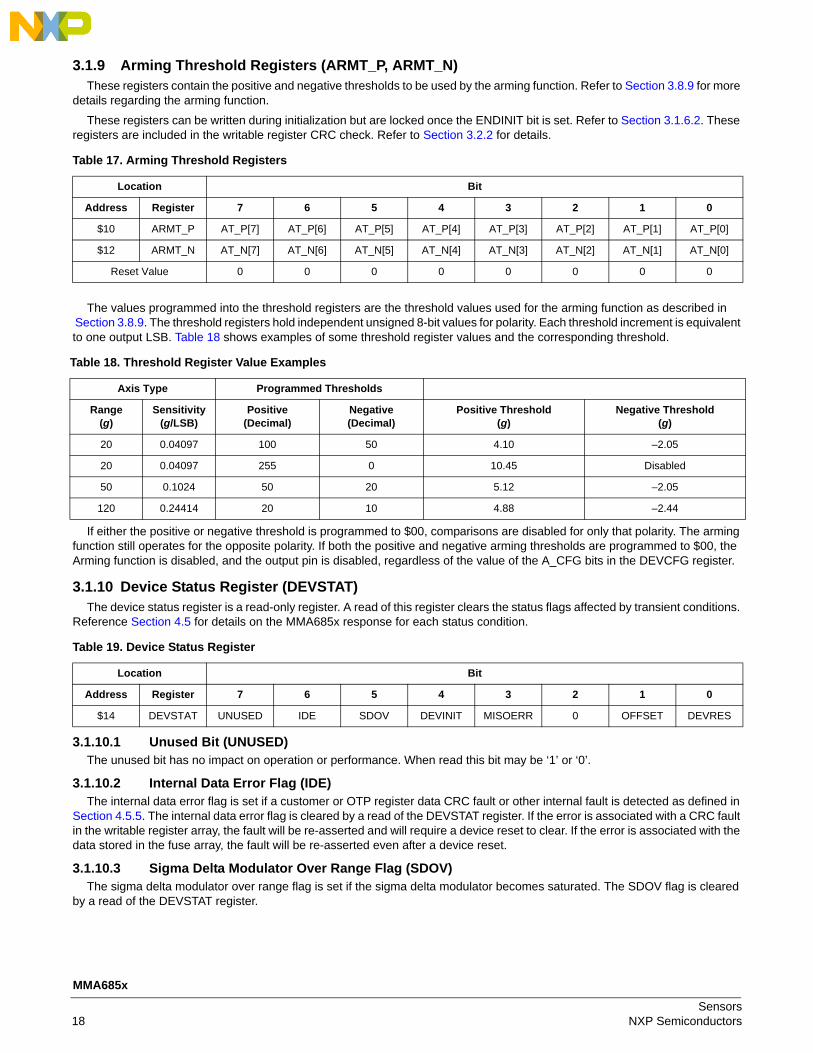
3.1.9 Arming Threshold Registers (ARMT_P, ARMT_N)These registers contain the positive and negative thresholds to be used by the arming function. Refer to Section 3.8.9 for more
details regarding the arming function.
These registers can be written during initialization but are locked once the ENDINIT bit is set. Refer to Section 3.1.6.2. These registers are included in the writable register CRC check. Refer to Section 3.2.2 for details.
The values programmed into the threshold registers are the threshold values used for the arming function as described in Section 3.8.9. The threshold registers hold independent unsigned 8-bit values for polarity. Each threshold increment is equivalent to one output LSB. Table 18 shows examples of some threshold register values and the corresponding threshold.
If either the positive or negative threshold is programmed to $00, comparisons are disabled for only that polarity. The arming function still operates for the opposite polarity. If both the positive and negative arming thresholds are programmed to $00, the Arming function is disabled, and the output pin is disabled, regardless of the value of the A_CFG bits in the DEVCFG register.
3.1.10 Device Status Register (DEVSTAT)The device status register is a read-only register. A read of this register clears the status flags affected by transient conditions.
Reference Section 4.5 for details on the MMA685x response for each status condition.
3.1.10.1 Unused Bit (UNUSED)The unused bit has no impact on operation or performance. When read this bit may be ‘1’ or ‘0’.
3.1.10.2 Internal Data Error Flag (IDE)The internal data error flag is set if a customer or OTP register data CRC fault or other internal fault is detected as defined in
Section 4.5.5. The internal data error flag is cleared by a read of the DEVSTAT register. If the error is associated with a CRC fault in the writable register array, the fault will be re-asserted and will require a device reset to clear. If the error is associated with the data stored in the fuse array, the fault will be re-asserted even after a device reset.
3.1.10.3 Sigma Delta Modulator Over Range Flag (SDOV)The sigma delta modulator over range flag is set if the sigma delta modulator becomes saturated. The SDOV flag is cleared
by a read of the DEVSTAT register.
Table 17. Arming Threshold Registers
Location Bit
Address Register 7 6 5 4 3 2 1 0
$10 ARMT_P AT_P[7] AT_P[6] AT_P[5] AT_P[4] AT_P[3] AT_P[2] AT_P[1] AT_P[0]
$12 ARMT_N AT_N[7] AT_N[6] AT_N[5] AT_N[4] AT_N[3] AT_N[2] AT_N[1] AT_N[0]
Reset Value 0 0 0 0 0 0 0 0
Table 18. Threshold Register Value Examples
Axis Type Programmed Thresholds
Range(g)
Sensitivity(g/LSB)
Positive(Decimal)
Negative(Decimal)
Positive Threshold(g)
Negative Threshold(g)
20 0.04097 100 50 4.10 –2.05
20 0.04097 255 0 10.45 Disabled
50 0.1024 50 20 5.12 –2.05
120 0.24414 20 10 4.88 –2.44
Table 19. Device Status Register
Location Bit
Address Register 7 6 5 4 3 2 1 0
$14 DEVSTAT UNUSED IDE SDOV DEVINIT MISOERR 0 OFFSET DEVRES
Sensors18 NXP Semiconductors
MMA685x
3.1.10.4 Device Initialization Flag (DEVINIT)The device initialization flag is set during the interval between negation of internal reset and completion of internal device
initialization. DEVINIT is cleared automatically. The device initialization flag is not affected by a read of the DEVSTAT register.
3.1.10.5 SPI MISO Data Mismatch Error Flag (MISOERR)The MISO data mismatch flag is set when a MISO Data mismatch fault occurs as specified in Section 4.5.2. The MISOERR
flag is cleared by a read of the DEVSTAT register.
3.1.10.6 Offset Monitor Over Range Flags (OFFSET)The offset monitor over range flag is set if the acceleration signal reaches the specified offset limit. The offset monitor over
range flags are cleared by a read of the DEVSTAT register.
3.1.10.7 Device Reset Flag (DEVRES)The device reset flag is set during device initialization following a device reset. The device reset flag is cleared by a read of
the DEVSTAT register.
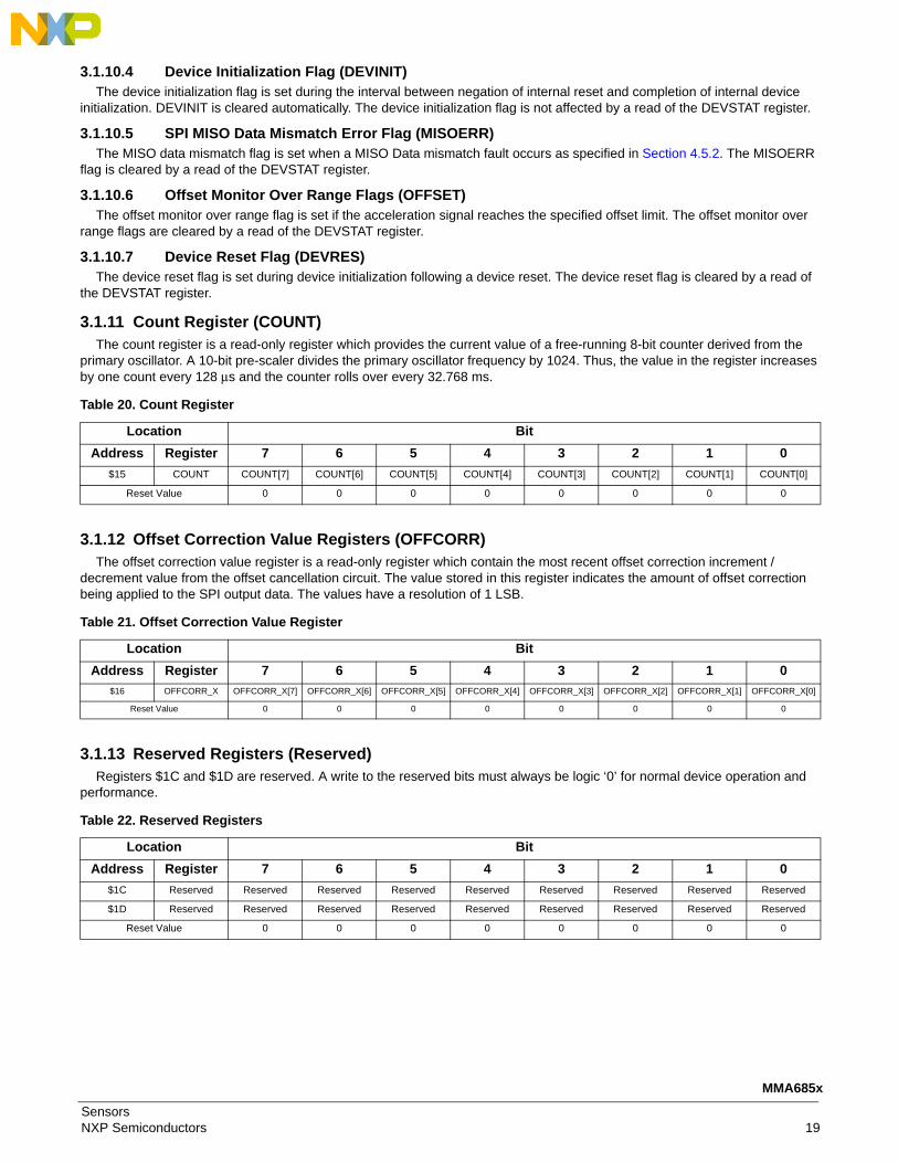
3.1.11 Count Register (COUNT)The count register is a read-only register which provides the current value of a free-running 8-bit counter derived from the
primary oscillator. A 10-bit pre-scaler divides the primary oscillator frequency by 1024. Thus, the value in the register increases by one count every 128 μs and the counter rolls over every 32.768 ms.
3.1.12 Offset Correction Value Registers (OFFCORR)The offset correction value register is a read-only register which contain the most recent offset correction increment /
decrement value from the offset cancellation circuit. The value stored in this register indicates the amount of offset correction being applied to the SPI output data. The values have a resolution of 1 LSB.
3.1.13 Reserved Registers (Reserved)Registers $1C and $1D are reserved. A write to the reserved bits must always be logic ‘0’ for normal device operation and
performance.
Table 20. Count Register
Location Bit
Address Register 7 6 5 4 3 2 1 0
$15 COUNT COUNT[7] COUNT[6] COUNT[5] COUNT[4] COUNT[3] COUNT[2] COUNT[1] COUNT[0]
Reset Value 0 0 0 0 0 0 0 0
Table 21. Offset Correction Value Register
Location Bit
Address Register 7 6 5 4 3 2 1 0
$16 OFFCORR_X OFFCORR_X[7] OFFCORR_X[6] OFFCORR_X[5] OFFCORR_X[4] OFFCORR_X[3] OFFCORR_X[2] OFFCORR_X[1] OFFCORR_X[0]
Reset Value 0 0 0 0 0 0 0 0
Table 22. Reserved Registers
Location Bit
Address Register 7 6 5 4 3 2 1 0
$1C Reserved Reserved Reserved Reserved Reserved Reserved Reserved Reserved Reserved
$1D Reserved Reserved Reserved Reserved Reserved Reserved Reserved Reserved Reserved
Reset Value 0 0 0 0 0 0 0 0
SensorsNXP Semiconductors 19
MMA685x
3.2 Customer Accessible Data Array CRC Verification
3.2.1 OTP Shadow Register Array CRC VerificationThe OTP shadow register array is verified for errors using a 3-bit CRC. The CRC verification uses a generator polynomial of
g(x) = X 3+ X + 1, with a seed value = ‘111’. If a CRC error is detected in the OTP array, the IDE bit is set in the DEVSTAT register.
3.2.2 Writable Register CRC VerificationThe writable registers in the data array are verified for errors using a 3-bit CRC. The CRC verification is enabled only when
the ENDINIT bit is set in the DEVCFG register. The CRC verification uses a generator polynomial of g(x) = X3 + X + 1, with a seed value = ‘111’. If a CRC error is detected in the writable register array, the IDE bit is set in the DEVSTAT register.
Sensors20 NXP Semiconductors
MMA685x
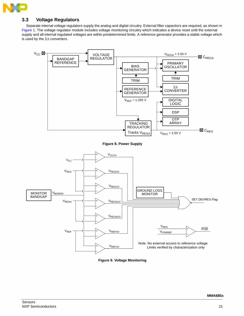
3.3 Voltage RegulatorsSeparate internal voltage regulators supply the analog and digital circuitry. External filter capacitors are required, as shown in
Figure 1. The voltage regulator module includes voltage monitoring circuitry which indicates a device reset until the external supply and all internal regulated voltages are within predetermined limits. A reference generator provides a stable voltage which is used by the ΣΔ converters.
Figure 8. Power Supply
Figure 9. Voltage Monitoring
CREGA
CREG
VCC
TRACKINGREGULATOR
VOLTAGEREGULATOR
REFERENCEGENERATOR
VREGA = 2.50 V
DIGITALLOGIC
DSP
OTPARRAY
PRIMARYOSCILLATOR
ΣΔCONVERTER
BIASGENERATOR
TRIMTRIM
VREF = 1.250 V
VREG = 2.50 V
BANDGAPREFERENCE
Tracks VREGA
SET DEVRES Flag
VCC
VREGA
VREG
VREF
MONITORBANDGAP
VCCUV
VREGOV
VREGUV
VREGAUV
VREGAOV
VREFOV
VREFUV
GROUND LOSSMONITOR
VREGPOR
VBGMON
VPORREF
Note: No external access to reference voltageLimits verified by characterization only
SensorsNXP Semiconductors 21
MMA685x

3.3.1 CREG Failure DetectionThe digital supply voltage regulator is designed to be unstable with low capacitance. If the connection to the VREG capacitor
becomes open, the digital supply voltage will oscillate and cause either an undervoltage, or overvoltage failure within one internal sample time. This failure will result in one of the following:
1. The DEVRES flag in the DEVSTAT register will be set. MMA685x will respond to SPI acceleration requests as defined in Table 27.
2. MMA685x will be held in RESET and be non-responsive to SPI requests.
3.3.2 CREGA Failure DetectionThe analog supply voltage regulator is designed to be unstable with low capacitance. If the connection to the VREGA capacitor
becomes open, the analog supply voltage will oscillate and cause either an undervoltage, or overvoltage failure within one internal sample time. The DEVRES flag in the DEVSTAT register will be set. MMA685x will respond to SPI acceleration requests as defined in Table 27.Note: This feature is only supported with a VCC supply voltage in the range of 4.75 V to 5.25 V.
3.3.3 VSS and VSSA Ground Loss MonitorMMA685x detects the loss of ground connection to either VSS or VSSA. A loss of ground connection to VSS will result in a VREG
overvoltage failure. A loss of ground connection to VSSA will result in a VREG undervoltage failure. Both failures result in a device reset.
3.3.4 SPI Initiated ResetIn addition to voltage monitoring, a device reset can be initiated by a specific series of three write operations involving the
RES_1 and RES_0 bits in the DEVCTL register. Reference Section 3.1.5.1. for details regarding the SPI initiated reset.
3.4 Internal OscillatorMMA685x includes a factory trimmed oscillator as specified in Section 2.6.
3.4.1 Oscillator MonitorThe COUNT register in the customer accessible array is a read-only register which provides the current value of a free-running
8-bit counter derived from the primary oscillator. A 10-bit pre-scaler divides the primary oscillator by 1024. Thus, the value in the COUNT register increases by one count every 128 μs, and the register rolls over every 32.768 ms. The SPI master can periodically read the COUNT register, and verify the difference between subsequent register reads against the system time base.
1. The SPI access rates and deviations must be taken into account for this oscillator verification.
Sensors22 NXP Semiconductors
MMA685x
3.5 TransducerThe MMA685x transducer is an overdamped mass-spring-damper system described by the following transfer function:
where:
ζ = Damping Ratioωn = Natural Frequency = 2∗Π∗fn
Reference Section 2.4 for transducer parameters.
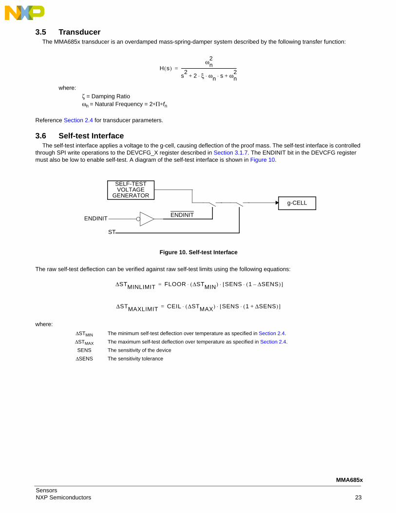
3.6 Self-test InterfaceThe self-test interface applies a voltage to the g-cell, causing deflection of the proof mass. The self-test interface is controlled
through SPI write operations to the DEVCFG_X register described in Section 3.1.7. The ENDINIT bit in the DEVCFG register must also be low to enable self-test. A diagram of the self-test interface is shown in Figure 10.
Figure 10. Self-test Interface
The raw self-test deflection can be verified against raw self-test limits using the following equations:
where:
ΔSTMIN The minimum self-test deflection over temperature as specified in Section 2.4.
ΔSTMAX The maximum self-test deflection over temperature as specified in Section 2.4.
SENS The sensitivity of the device
ΔSENS The sensitivity tolerance
H s( )ωn
2
s2
2 ξ ωn s⋅ ⋅ ⋅ ωn2
+ +---------------------------------------------------------=
SELF-TESTVOLTAGE
GENERATOR
ENDINIT
ST
g-CELL
ENDINIT
ΔSTMINLIMIT FLOOR ΔSTMIN( ) SENS 1 ΔSENS–( )⋅[ ]⋅⋅=
ΔSTMAXLIMIT CEIL ΔSTMAX( ) SENS 1 ΔSENS+( )⋅[ ]⋅ ⋅=
SensorsNXP Semiconductors 23
MMA685x
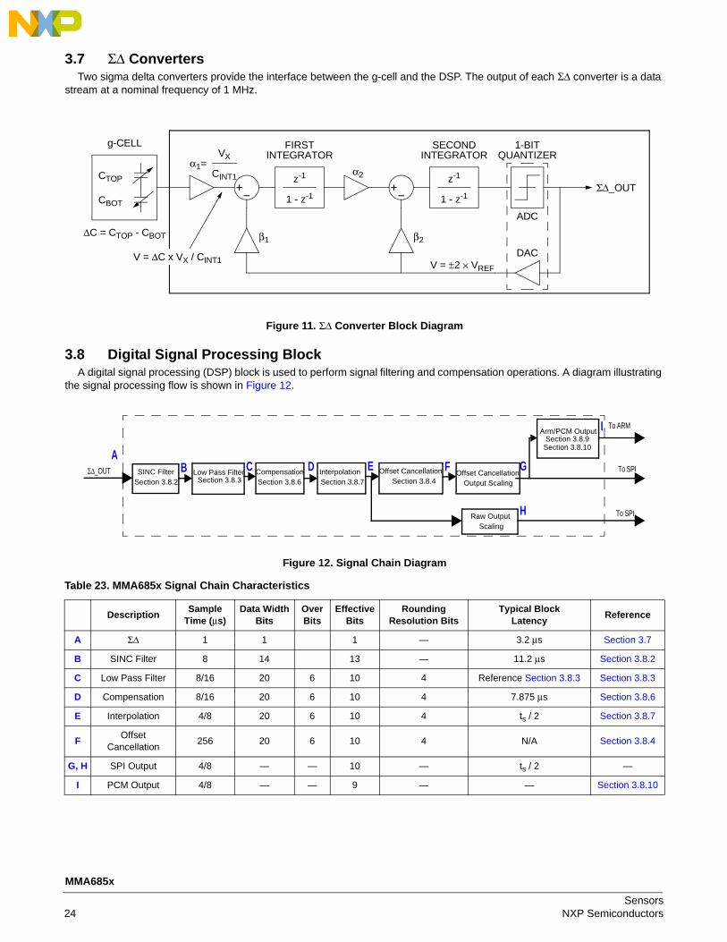
3.7 ΣΔ ConvertersTwo sigma delta converters provide the interface between the g-cell and the DSP. The output of each ΣΔ converter is a data
stream at a nominal frequency of 1 MHz.
Figure 11. ΣΔ Converter Block Diagram
3.8 Digital Signal Processing BlockA digital signal processing (DSP) block is used to perform signal filtering and compensation operations. A diagram illustrating
the signal processing flow is shown in Figure 12.
Figure 12. Signal Chain Diagram
1-BITQUANTIZER
z-1
1 - z-1
z-1
1 - z-1
FIRSTINTEGRATOR
SECONDINTEGRATOR
α1=
β1
α2
β2
VX
CINT1
g-CELL
CBOT
CTOP
ΔC = CTOP - CBOT
ΣΔ_OUT
V = ±2 × VREF
ADC
DACV = ΔC x VX / CINT1
ΣΔ_OUT
To SPI
To ARM
AB C E G To SPI
H
I
D FSINC FilterSection 3.8.2
Low Pass FilterSection 3.8.3
CompensationSection 3.8.6
InterpolationSection 3.8.7
Offset CancellationSection 3.8.4
Offset CancellationOutput Scaling
Raw OutputScaling
Arm/PCM OutputSection 3.8.9
Section 3.8.10
Table 23. MMA685x Signal Chain Characteristics
DescriptionSample
Time (μs)Data Width
BitsOver Bits
EffectiveBits
RoundingResolution Bits
Typical BlockLatency
Reference
A ΣΔ 1 1 1 — 3.2 μs Section 3.7
B SINC Filter 8 14 13 — 11.2 μs Section 3.8.2
C Low Pass Filter 8/16 20 6 10 4 Reference Section 3.8.3 Section 3.8.3
D Compensation 8/16 20 6 10 4 7.875 μs Section 3.8.6
E Interpolation 4/8 20 6 10 4 ts / 2 Section 3.8.7
FOffset
Cancellation256 20 6 10 4 N/A Section 3.8.4
G, H SPI Output 4/8 — — 10 — ts / 2 —
I PCM Output 4/8 — — 9 — — Section 3.8.10
Sensors24 NXP Semiconductors
MMA685x
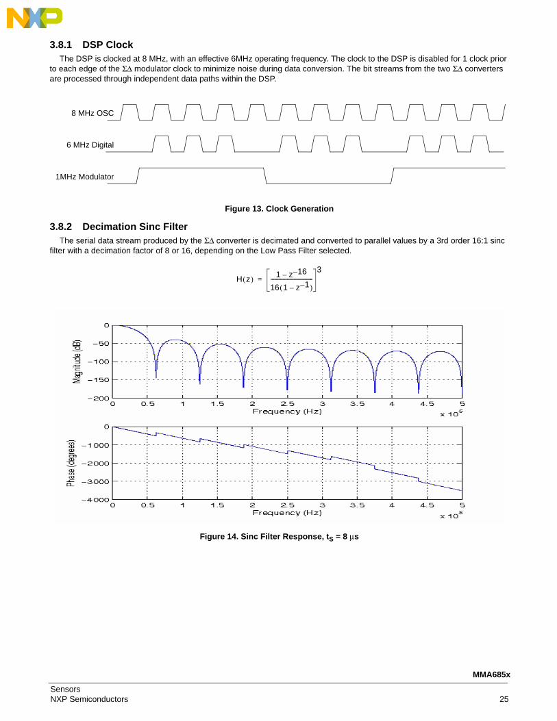
3.8.1 DSP ClockThe DSP is clocked at 8 MHz, with an effective 6MHz operating frequency. The clock to the DSP is disabled for 1 clock prior
to each edge of the ΣΔ modulator clock to minimize noise during data conversion. The bit streams from the two ΣΔ converters are processed through independent data paths within the DSP.
Figure 13. Clock Generation
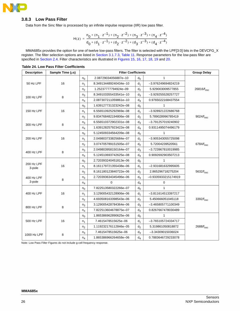
3.8.2 Decimation Sinc FilterThe serial data stream produced by the ΣΔ converter is decimated and converted to parallel values by a 3rd order 16:1 sinc
filter with a decimation factor of 8 or 16, depending on the Low Pass Filter selected.
Figure 14. Sinc Filter Response, tS = 8 μs
8 MHz OSC
6 MHz Digital
1MHz Modulator
H z( ) 1 z 16––
16 1 z 1––( )-------------------------------
3=
SensorsNXP Semiconductors 25
MMA685x
3.8.3 Low Pass FilterData from the Sinc filter is processed by an infinite impulse response (IIR) low pass filter.
MMA685x provides the option for one of twelve low-pass filters. The filter is selected with the LPF[3:0] bits in the DEVCFG_X register. The filter selection options are listed in Section 3.1.7.3, Table 11. Response parameters for the low-pass filter are specified in Section 2.4. Filter characteristics are illustrated in Figures 15, 16, 17, 18, 19 and 20.
Note: Low Pass Filter Figures do not include g-cell frequency response.
Table 24. Low Pass Filter Coefficients
Description Sample Time (μs) Filter Coefficients Group Delay
50 Hz LPF 16
n0 2.08729034056887e–10 d0 1
26816/fosc
n1 8.349134489240434e–10 d1 –3.976249694824219
n2 1.25237777794924e–09 d2 5.929003009577855
100 Hz LPF 8n3 8.349103355433541e–10 d3 –3.929255528257727
n4 2.087307211059861e–10 d4 0.9765022168437554
150 Hz LPF 16
n0 1.639127731323242e–08 d0 1
9024/fosc
n1 6.556510925292969e–08 d1 –3.928921222686768
n2 9.834768482194806e–08 d2 5.789028996785419
300 Hz LPF 8n3 6.556510372902331e–08 d3 –3.791257019240902
n4 1.639128257923422e–08 d4 0.9311495074496179
200 Hz LPF 16
n0 5.124509334564209e–08 d0 1
6784/fosc
n1 2.049803733825684e–07 d1 –3.905343055725098
n2 3.074705789151505e–07 d2 5.72004239520561
400 Hz LPF 8n3 2.049803958150164e–07 d3 –3.723967810019985
n4 5.124510693742625e–08 d4 0.9092692903507213
200 Hz LPF3-pole
16
n0 2.720393240451813e–06 d0 1
5632/fosc
n1 8.161179721355438e–06 d1 –2.931681632995605
n2 8.161180123840722e–06 d2 2.865296718275204
400 Hz LPF3-pole
8n3 2.720393634345496e–06 d3 –0.9335933215174919
n4 0 d4 0
400 Hz LPF 16
n0 7.822513580322266e–07 d0 1
3392/fosc
n1 3.129005432128906e–06 d1 –3.811614513397217
n2 4.693508163398543e–06 d2 5.450666051045118
800 Hz LPF 8n3 3.129005428784364e–06 d3 –3.465805771100349
n4 7.822513604678875e–07 d4 0.8267667478030489
500 Hz LPF 16
n0 1.865386962890625e–06 d0 1
2688/fosc
n1 7.4615478515625e–06 d1 –3.765105724334717
n2 1.119232176112846e–05 d2 5.319861050818872
1000 Hz LPF 8n3 7.4615478515625e–06 d3 –3.34309015036024
n4 1.865386966264658e–06 d4 0.7883646729233078
H z( )n0 n1 z 1–⋅( ) n2 z 2–⋅( ) n3 z 3–⋅( ) n4 z 4–⋅( )+ + + +
d0 d1 z 1–⋅( ) d2 z 2–⋅( ) d3 z 3–⋅( ) d4 z 4–⋅( )+ + + +-----------------------------------------------------------------------------------------------------------------------------------------=
Sensors26 NXP Semiconductors
MMA685x
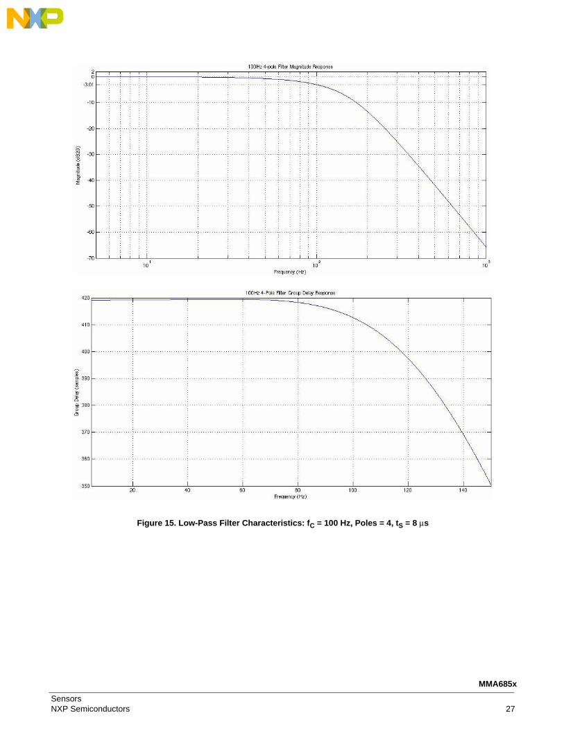
Figure 15. Low-Pass Filter Characteristics: fC = 100 Hz, Poles = 4, tS = 8 μs
SensorsNXP Semiconductors 27
MMA685x
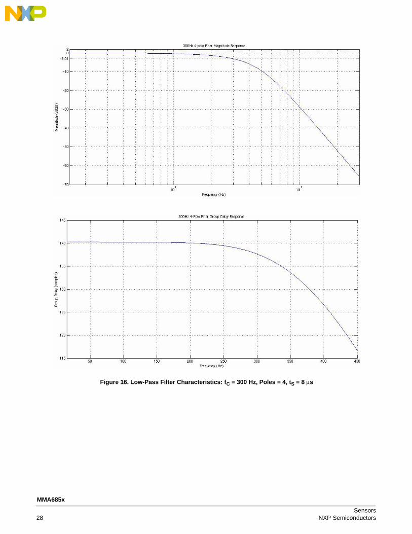
Figure 16. Low-Pass Filter Characteristics: fC = 300 Hz, Poles = 4, tS = 8 μs
Sensors28 NXP Semiconductors
MMA685x
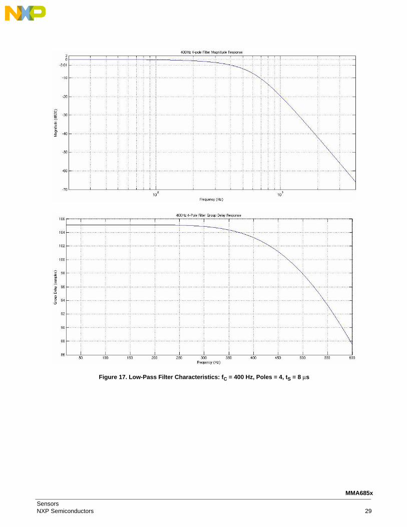
Figure 17. Low-Pass Filter Characteristics: fC = 400 Hz, Poles = 4, tS = 8 μs
SensorsNXP Semiconductors 29
MMA685x
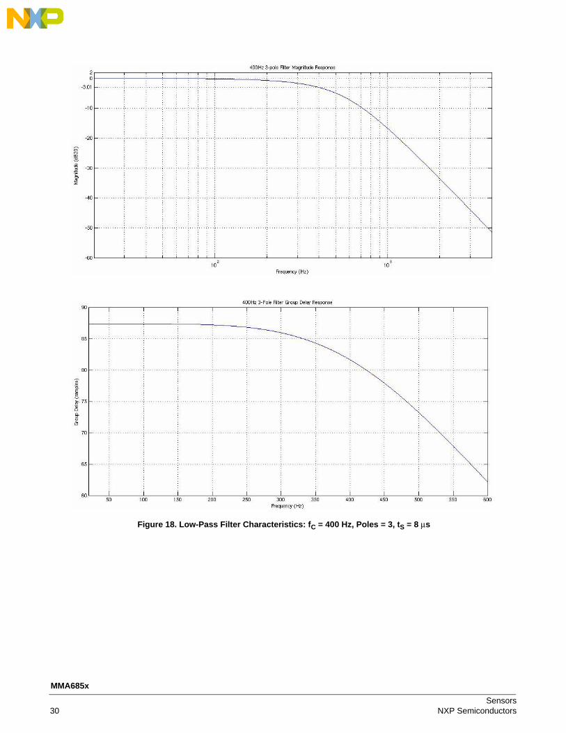
Figure 18. Low-Pass Filter Characteristics: fC = 400 Hz, Poles = 3, tS = 8 μs
Sensors30 NXP Semiconductors
MMA685x
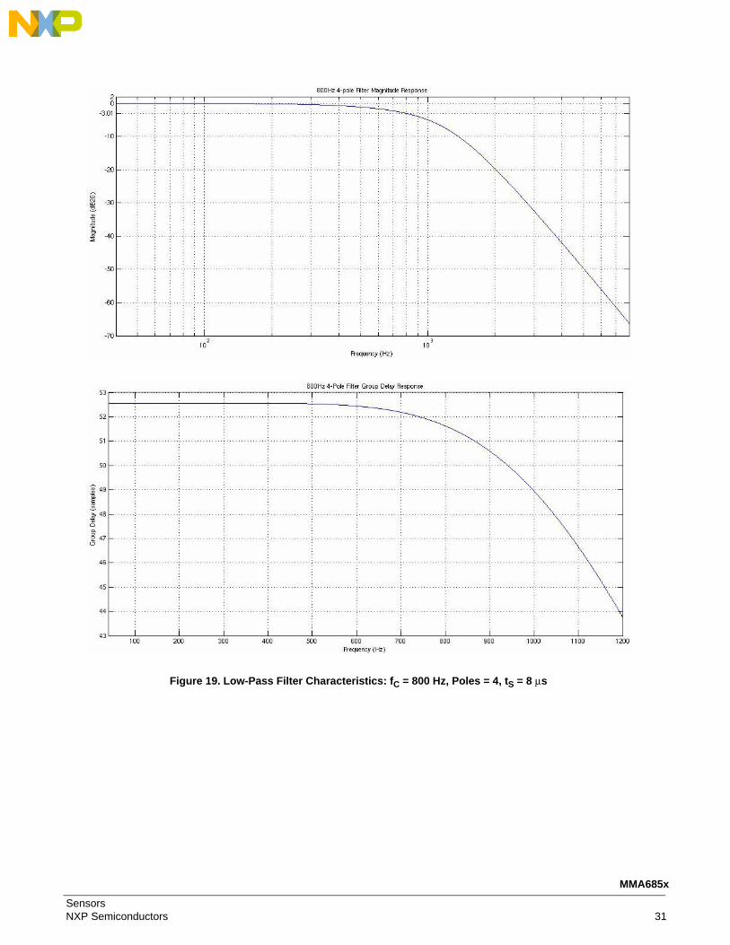
Figure 19. Low-Pass Filter Characteristics: fC = 800 Hz, Poles = 4, tS = 8 μs
SensorsNXP Semiconductors 31
MMA685x
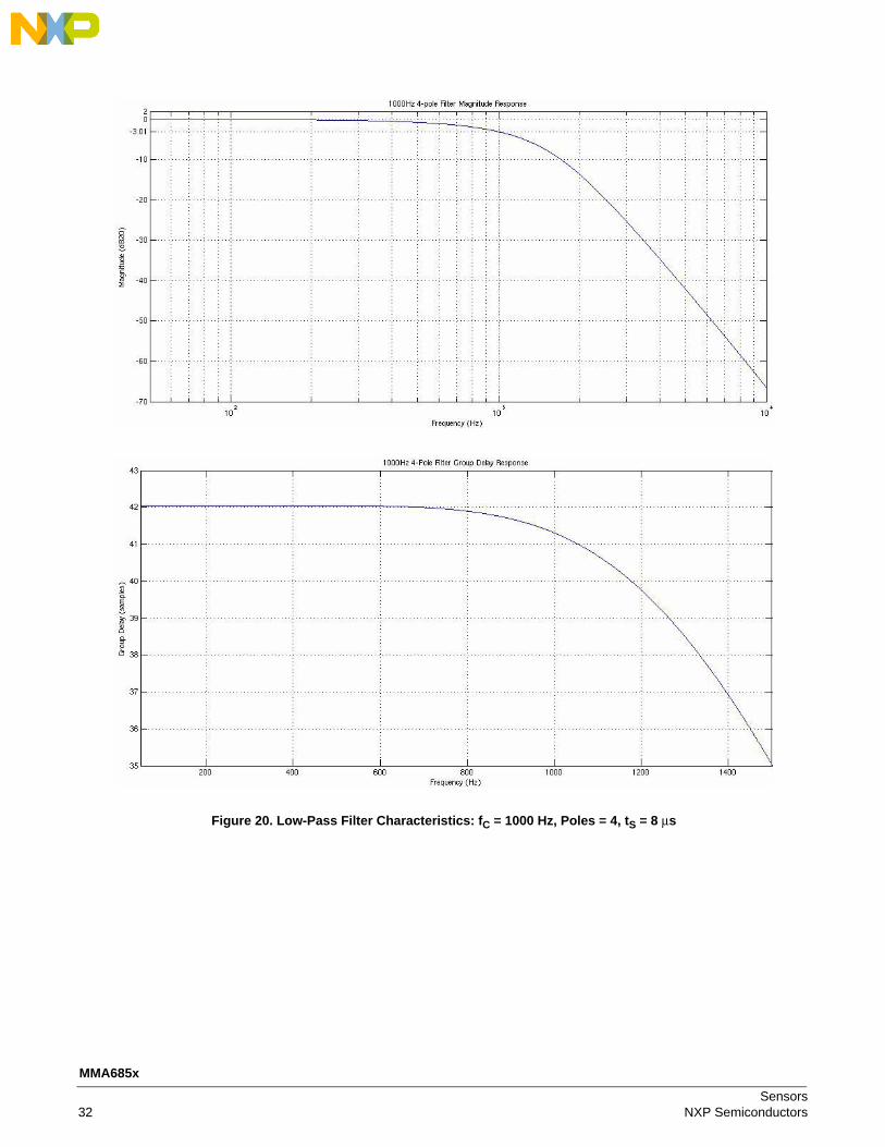
Figure 20. Low-Pass Filter Characteristics: fC = 1000 Hz, Poles = 4, tS = 8 μs
Sensors32 NXP Semiconductors
MMA685x

3.8.4 Offset CancellationMMA685x provides the option to read offset cancelled acceleration data via the SPI by clearing the OC bit in the SPI command
(reference Section 4.1). A block diagram of the offset cancellation is shown in Figure 21, and response parameters are specified in Section 2.4 and in Table 25.
Figure 21. Offset Cancellation Block Diagram
In normal operation, the offset cancellation circuit computes a 24,576 sample running average of the acceleration data downsampled to 256 μs. The running average is compared against positive and negative thresholds to determine the offset correction value that will be applied to the acceleration data.
During start up, three phases of moving average sizes are used to allow for faster convergence of misuse input signals. Refer to Table 25 for offset cancellation timing information during startup and normal operation.
When the self-test circuitry is active, the offset cancellation block and the offset monitor block are suspended, and the offset correction value is constant. Once the self-test circuitry is disabled, the offset cancellation block remains suspended for the time tST_OMB to allow the acceleration output to return to its nominal offset.
3.8.5 Offset MonitorMMA685x provides the option for an offset monitor circuit. The offset monitor circuit is enabled when the OFMON bit in the
DEVCFG register is programmed to a logic ‘1’. The output of the offset cancellation circuit is compared against a high and low threshold. If the offset correction value exceeds either the OFFTHRPOS, or OFFTHRNEG threshold, an Offset Over Range condition is indicated.
The offset correction value update rate is listed in Table 25. Because the offset monitor uses this value, the offset monitor will also update at this rate. The time to indicate an Offset Over Range is dependent upon the input signal.
The offset monitor status remains frozen during self-test, because the offset monitor is based on the offset cancellation circuit, which is also suspended during self-test. The offset monitor is disabled for 2.1 seconds following reset regardless of the state of the OFMON bit.
3.8.6 Signal CompensationMMA685x includes internal OTP and signal processing to compensate for sensitivity error and offset error. This compensation
is necessary to achieve the specified parameters in Section 2.4.
Table 25. Offset Cancellation Timing Specifications
PhaseStart Time of
Phase(from POR)
TypicalTime in Phase
(ms)
# of Samples in Phase
SamplesAveraged
OFF_CORR_VALUEUpdate Rate
(ms)
Averaging Period(ms)
Maximum Slew Rate
(LSB/s)
Averaging Filter–3 dB Frequency
(Hz)
Start 1 tOP 524.288 2048 48 2.048 12.288 122.1 36.05
Start 2 tOP + 524.288 524.288 2048 384 16.38 98.304 15.26 4.506
Start 3 tOP + 1048.576 524.288 2048 3072 131.1 786.432 1.907 0.5632
Normal tOP + 1572.864 — — 24576 1049 6291.456 0.2384 0.07040
AccumulatorT1
up to 4096 samplesShift
LPFOUT T2 T5T4T3 T6
Offset Inc/DecOFFCORRP
OFFCORRN
OFFTHN
OFFTHP
INC
DEC
Downsampled to 256μs
OFF_CORR_VALUE
OFFTHRNEG
OFFTHRPOS
OFF_ERR
OFF_ERR
Correctionfor Start Phase
OCOUT
SensorsNXP Semiconductors 33
MMA685x
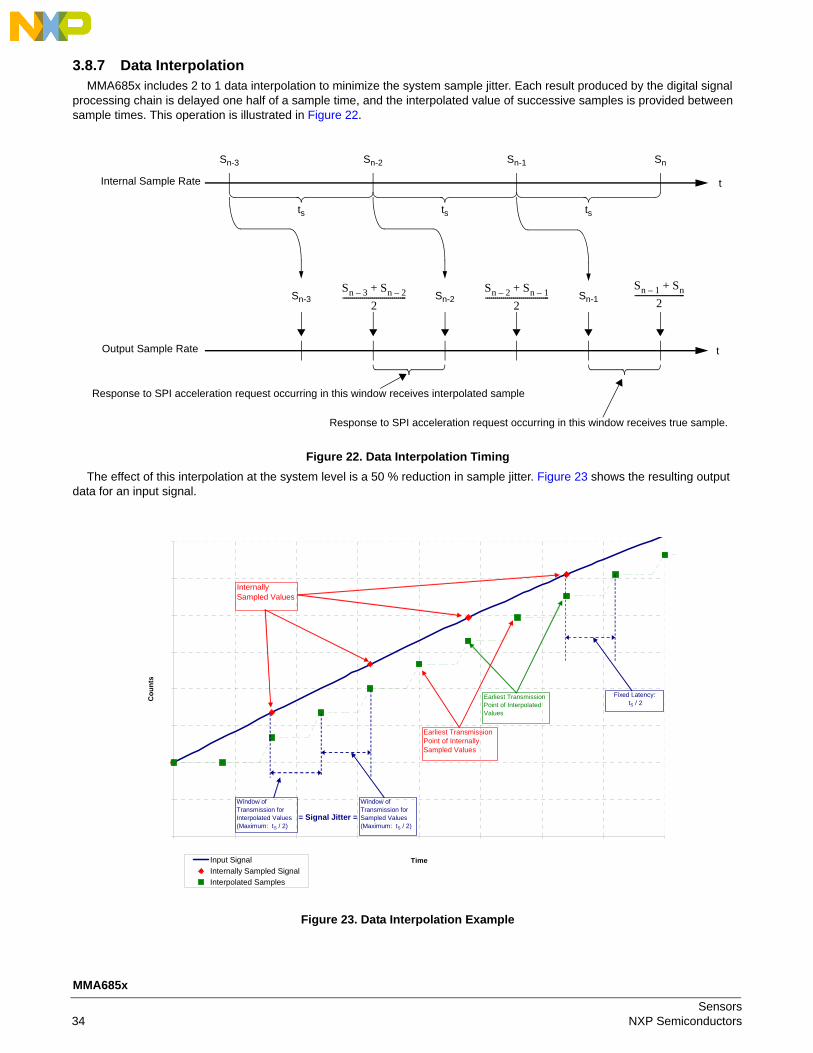
3.8.7 Data InterpolationMMA685x includes 2 to 1 data interpolation to minimize the system sample jitter. Each result produced by the digital signal
processing chain is delayed one half of a sample time, and the interpolated value of successive samples is provided between sample times. This operation is illustrated in Figure 22.
Figure 22. Data Interpolation Timing
The effect of this interpolation at the system level is a 50 % reduction in sample jitter. Figure 23 shows the resulting output data for an input signal.
Figure 23. Data Interpolation Example
Sn-3 Sn-2
t
t
Sn-1
ts ts
Sn-1
ts
Sn
Sn-2Sn 3– Sn 2–+
2--------------------------------
Sn 2– Sn 1–+
2--------------------------------
Sn 1– Sn+
2-------------------------Sn-3
Response to SPI acceleration request occurring in this window receives interpolated sample
Response to SPI acceleration request occurring in this window receives true sample.
Internal Sample Rate
Output Sample Rate
40
45
50
55
60
65
70
75
80
0 5 10 15 20 25 30 35 40
Time
Co
un
ts
Input Signal
Internally Sampled Signal
Interpolated Samples
Internally Sampled Values
Earliest Transmission Point of Interpolated Values
Earliest Transmission Point of Internally Sampled Values
Window of Transmission for Sampled Values (Maximum: tS / 2)
Window of Transmission for Interpolated Values (Maximum: tS / 2)
Fixed Latency: tS / 2
= Signal Jitter =
Sensors34 NXP Semiconductors
MMA685x
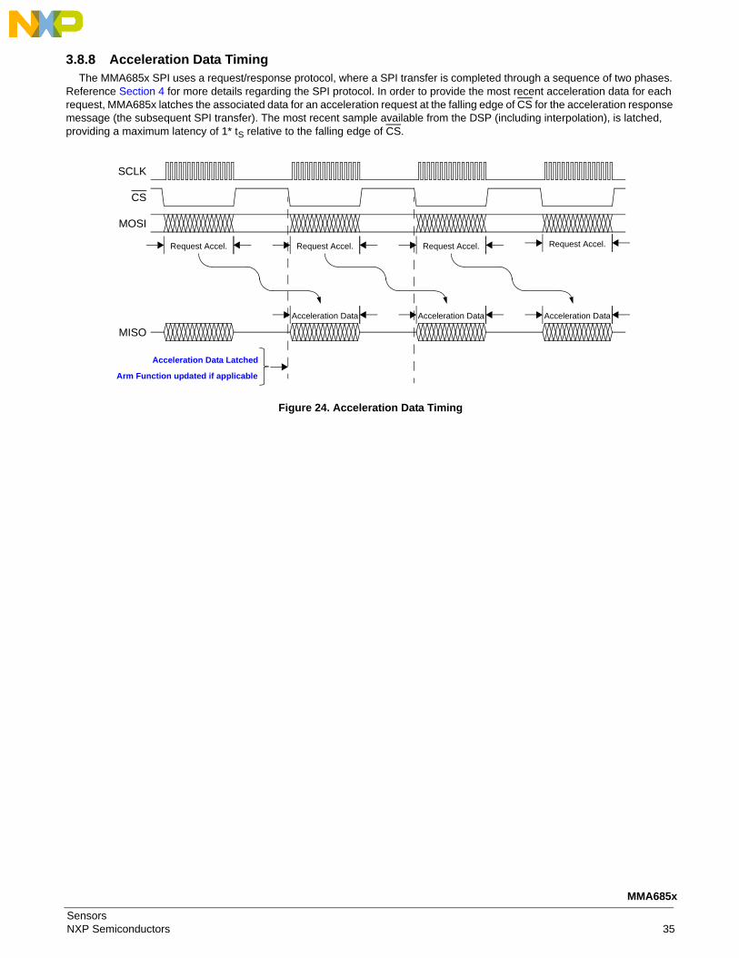
3.8.8 Acceleration Data TimingThe MMA685x SPI uses a request/response protocol, where a SPI transfer is completed through a sequence of two phases.
Reference Section 4 for more details regarding the SPI protocol. In order to provide the most recent acceleration data for each request, MMA685x latches the associated data for an acceleration request at the falling edge of CS for the acceleration response message (the subsequent SPI transfer). The most recent sample available from the DSP (including interpolation), is latched, providing a maximum latency of 1* tS relative to the falling edge of CS.
Figure 24. Acceleration Data Timing
SCLK
MOSI
MISO
CS
Request Accel. Request Accel.
Acceleration Data Acceleration Data
Request Accel. Request Accel.
Acceleration Data
Acceleration Data Latched
Arm Function updated if applicable
SensorsNXP Semiconductors 35
MMA685x
3.8.9 Arming FunctionMMA685x provides the option for an arming function with three modes of operation. The operation of the arming function is
selected by the state of the A_CFG bits in the DEVCFG register.
Reference Section 4.5 for the operation of the Arming function with exception conditions. Error conditions do not impact prior arming function responses. If an error occurs after an arming activation, the corresponding pulse stretch for the existing arming condition will continue. However, new acceleration reads will not update the arming function regardless of the acceleration value.
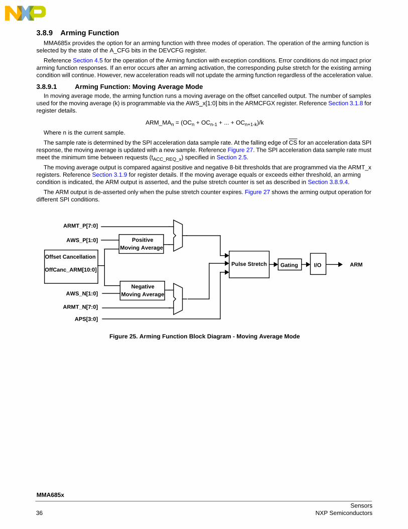
3.8.9.1 Arming Function: Moving Average ModeIn moving average mode, the arming function runs a moving average on the offset cancelled output. The number of samples
used for the moving average (k) is programmable via the AWS_x[1:0] bits in the ARMCFGX register. Reference Section 3.1.8 for register details.
ARM_MAn = (OCn + OCn-1 + ... + OCn+1-k)/k
Where n is the current sample.
The sample rate is determined by the SPI acceleration data sample rate. At the falling edge of CS for an acceleration data SPI response, the moving average is updated with a new sample. Reference Figure 27. The SPI acceleration data sample rate must meet the minimum time between requests (tACC_REQ_x) specified in Section 2.5.
The moving average output is compared against positive and negative 8-bit thresholds that are programmed via the ARMT_x registers. Reference Section 3.1.9 for register details. If the moving average equals or exceeds either threshold, an arming condition is indicated, the ARM output is asserted, and the pulse stretch counter is set as described in Section 3.8.9.4.
The ARM output is de-asserted only when the pulse stretch counter expires. Figure 27 shows the arming output operation for different SPI conditions.
Figure 25. Arming Function Block Diagram - Moving Average Mode
Offset Cancellation
AWS_P[1:0]
APS[3:0]
Pulse Stretch ARMGating I/O
ARMT_N[7:0]
ARMT_P[7:0]
Moving Average
Positive
Moving Average
NegativeAWS_N[1:0]
OffCanc_ARM[10:0]
Sensors36 NXP Semiconductors
MMA685x
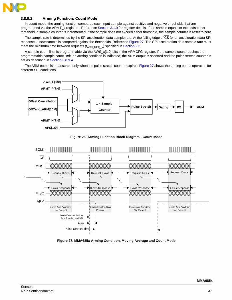
3.8.9.2 Arming Function: Count ModeIn count mode, the arming function compares each input sample against positive and negative thresholds that are
programmed via the ARMT_x registers. Reference Section 3.1.9 for register details. If the sample equals or exceeds either threshold, a sample counter is incremented. If the sample does not exceed either threshold, the sample counter is reset to zero.
The sample rate is determined by the SPI acceleration data sample rate. At the falling edge of CS for an acceleration data SPI response, a new sample is compared against the thresholds. Reference Figure 27. The SPI acceleration data sample rate must meet the minimum time between requests (tACC_REQ_x) specified in Section 2.5.
A sample count limit is programmable via the AWS_x[1:0] bits in the ARMCFG register. If the sample count reaches the programmable sample count limit, an arming condition is indicated, the ARM output is asserted and the pulse stretch counter is set as described in Section 3.8.9.4.
The ARM output is de-asserted only when the pulse stretch counter expires. Figure 27 shows the arming output operation for different SPI conditions.
Figure 26. Arming Function Block Diagram - Count Mode
Figure 27. MMA685x Arming Condition, Moving Average and Count Mode
ARMT_N[7:0]
Offset Cancellation
AWS_P[1:0]
APS[1:0]
Pulse Stretch ARM
ARMT_P[7:0]
Gating I/O1-4 Sample
CounterOffCanc_ARM[10:0]
X-axis Arm ConditionNot Present
X-axis Data Latched for Arm Function and SPI
SCLK
MOSI
MISO
CS
Request X-axis Request X-axis
X-axis Response X-axis Response
Request X-axis Request X-axis
X-axis Response
ARM
X-axis Response
X-axis Arm ConditionNot Present
X-axis Arm ConditionNot Present
X-axis Arm ConditionPresent
tARM
Pulse Stretch Time
SensorsNXP Semiconductors 37
MMA685x
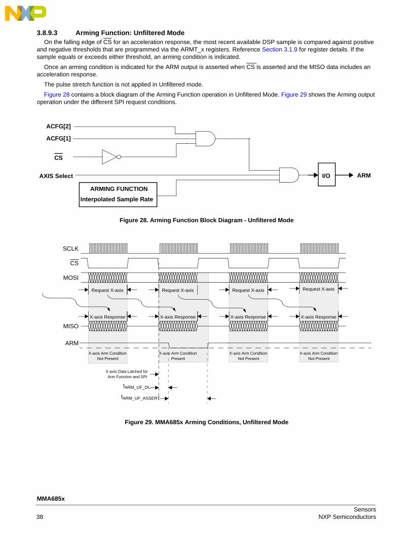
3.8.9.3 Arming Function: Unfiltered ModeOn the falling edge of CS for an acceleration response, the most recent available DSP sample is compared against positive
and negative thresholds that are programmed via the ARMT_x registers. Reference Section 3.1.9 for register details. If the sample equals or exceeds either threshold, an arming condition is indicated.
Once an arming condition is indicated for the ARM output is asserted when CS is asserted and the MISO data includes an acceleration response.
The pulse stretch function is not applied in Unfiltered mode.
Figure 28 contains a block diagram of the Arming Function operation in Unfiltered Mode. Figure 29 shows the Arming output operation under the different SPI request conditions.
Figure 28. Arming Function Block Diagram - Unfiltered Mode
Figure 29. MMA685x Arming Conditions, Unfiltered Mode
ACFG[2]
CS
AXIS Select ARMI/O
ACFG[1]
ARMING FUNCTION
Interpolated Sample Rate
X-axis Arm ConditionNot Present
X-axis Data Latched for Arm Function and SPI
SCLK
MOSI
MISO
CS
Request X-axis Request X-axis
X-axis Response X-axis Response
Request X-axis Request X-axis
X-axis Response
ARM
X-axis Response
X-axis Arm ConditionNot Present
X-axis Arm ConditionNot Present
X-axis Arm ConditionPresent
tARM_UF_DL
tARM_UF_ASSERT
Sensors38 NXP Semiconductors
MMA685x
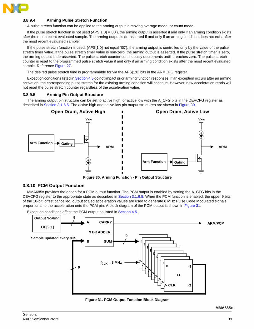
3.8.9.4 Arming Pulse Stretch FunctionA pulse stretch function can be applied to the arming output in moving average mode, or count mode.
If the pulse stretch function is not used (APS[1:0] = ‘00’), the arming output is asserted if and only if an arming condition exists after the most recent evaluated sample. The arming output is de-asserted if and only if an arming condition does not exist after the most recent evaluated sample.
If the pulse stretch function is used, (APS[1:0] not equal ‘00’), the arming output is controlled only by the value of the pulse stretch timer value. If the pulse stretch timer value is non-zero, the arming output is asserted. If the pulse stretch timer is zero, the arming output is de-asserted. The pulse stretch counter continuously decrements until it reaches zero. The pulse stretch counter is reset to the programmed pulse stretch value if and only if an arming condition exists after the most recent evaluated sample. Reference Figure 27.
The desired pulse stretch time is programmable for via the APS[1:0] bits in the ARMCFG register.
Exception conditions listed in Section 4.5 do not impact prior arming function responses. If an exception occurs after an arming activation, the corresponding pulse stretch for the existing arming condition will continue. However, new acceleration reads will not reset the pulse stretch counter regardless of the acceleration value.
3.8.9.5 Arming Pin Output StructureThe arming output pin structure can be set to active high, or active low with the A_CFG bits in the DEVCFG register as
described in Section 3.1.6.5. The active high and active low pin output structures are shown in Figure 30.
Figure 30. Arming Function - Pin Output Structure
3.8.10 PCM Output FunctionMMA685x provides the option for a PCM output function. The PCM output is enabled by setting the A_CFG bits in the
DEVCFG register to the appropriate state as described in Section 3.1.6.5. When the PCM function is enabled, the upper 9 bits of the 10-bit, offset cancelled, output scaled acceleration values are used to generate 8 MHz Pulse Code Modulated signals proportional to the acceleration onto the PCM pin. A block diagram of the PCM output is shown in Figure 31.
Exception conditions affect the PCM output as listed in Section 4.5.
Figure 31. PCM Output Function Block Diagram
Arm Function
ARM
Gating
VCC
Arm FunctionARM
Gating
VCC
Open Drain, Active High Open Drain, Active Low
Output Scaling
OC[9:1]A
9 Bit ADDER
ARM/PCM
B
CARRY
SUM
fCLK = 8 MHz
Sample updated every 8μS9
9
D
FF
CLK
Q
Q
D
FF
CLK
Q
Q
D
FF
CLK
Q
Q
D
FF
CLK
Q
Q
D
FF
CLK
Q
Q
D
FF
CLK
Q
Q
D
FF
CLK
Q
Q
D
FF
CLK
Q
Q
D
FF
CLK
Q
Q
9
SensorsNXP Semiconductors 39
MMA685x
3.9 Serial Peripheral InterfaceMMA685x includes a Serial Peripheral Interface (SPI) to provide access to the configuration registers and digital data.
Reference Section 4 for details regarding the SPI protocol and available commands.
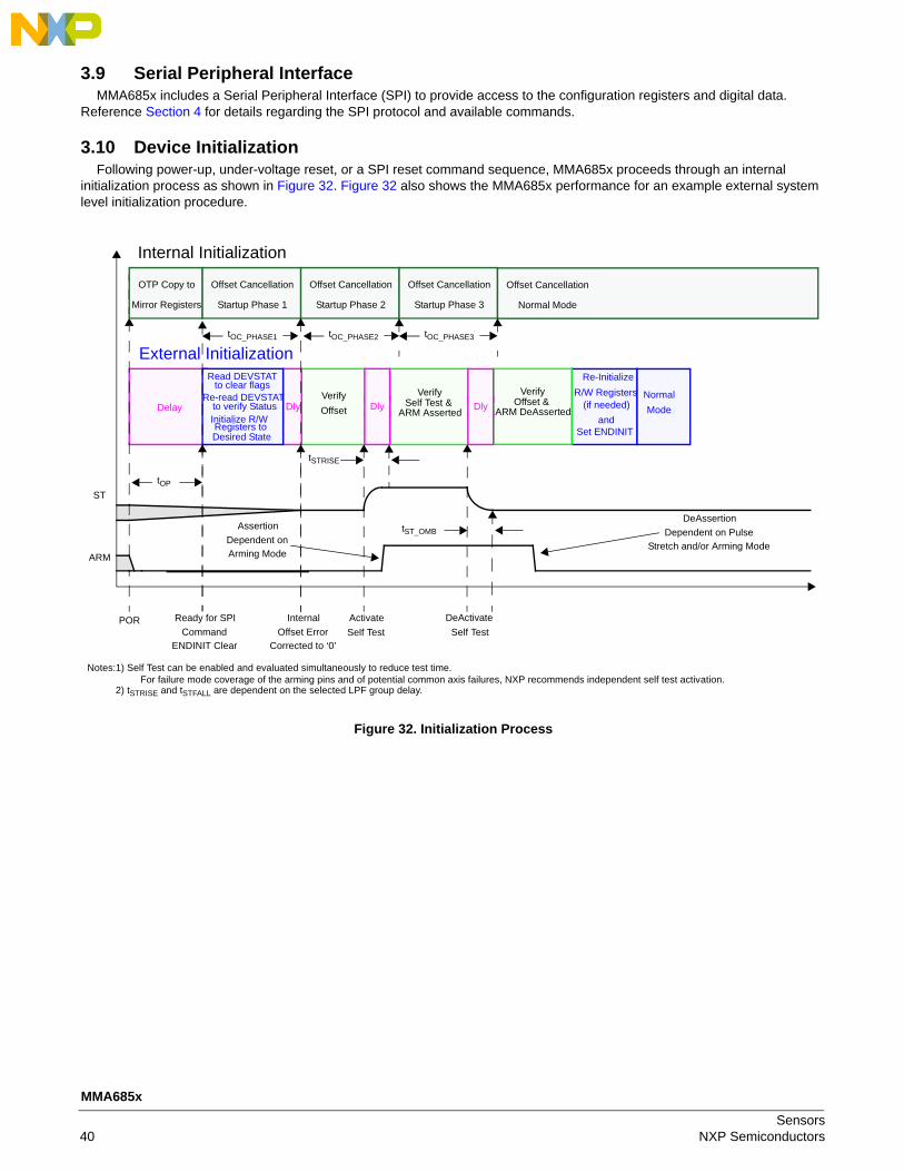
3.10 Device InitializationFollowing power-up, under-voltage reset, or a SPI reset command sequence, MMA685x proceeds through an internal
initialization process as shown in Figure 32. Figure 32 also shows the MMA685x performance for an example external system level initialization procedure.
Figure 32. Initialization Process
Dly
POR
OTP Copy to
Mirror Registers
Offset Cancellation
Startup Phase 2
Initialize R/W Registers to Desired State
Verify
Offset
VerifySelf Test &
ARM Asserted
Offset Cancellation
Startup Phase 1
Offset Cancellation
Startup Phase 3
Offset Cancellation
Normal Mode
Ready for SPI
Command
ENDINIT Clear
Dly
Re-Initialize
R/W Registers (if needed)
Activate
Self Test
Internal
Offset Error
Corrected to ‘0’
DeActivate
Self Test
Normal
Mode
Internal Initialization
External Initialization
Delay
DeAssertion
Dependent on Pulse
Stretch and/or Arming Mode
Assertion
Dependent on
Arming Mode
Set ENDINIT
Read DEVSTATto clear flags
Re-read DEVSTATto verify Status
tST_OMB
tOC_PHASE1 tOC_PHASE2 tOC_PHASE3
tOP
and
ST
ARM
Notes:1) Self Test can be enabled and evaluated simultaneously to reduce test time. For failure mode coverage of the arming pins and of potential common axis failures, NXP recommends independent self test activation.
tSTRISE
2) tSTRISE and tSTFALL are dependent on the selected LPF group delay.
VerifyOffset &
ARM DeAssertedDly
Sensors40 NXP Semiconductors
MMA685x
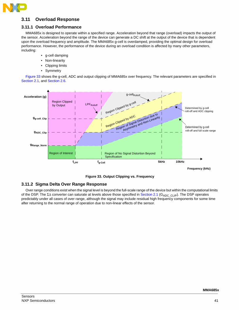
3.11 Overload Response
3.11.1 Overload PerformanceMMA685x is designed to operate within a specified range. Acceleration beyond that range (overload) impacts the output of
the sensor. Acceleration beyond the range of the device can generate a DC shift at the output of the device that is dependent upon the overload frequency and amplitude. The MMA685x g-cell is overdamped, providing the optimal design for overload performance. However, the performance of the device during an overload condition is affected by many other parameters, including:
• g-cell damping
• Non-linearity
• Clipping limits
• Symmetry
Figure 33 shows the g-cell, ADC and output clipping of MMA685x over frequency. The relevant parameters are specified in Section 2.1, and Section 2.6.
Figure 33. Output Clipping vs. Frequency
3.11.2 Sigma Delta Over Range ResponseOver range conditions exist when the signal level is beyond the full-scale range of the device but within the computational limits
of the DSP. The ΣΔ converter can saturate at levels above those specified in Section 2.1 (GADC_CLIP). The DSP operates predictably under all cases of over range, although the signal may include residual high frequency components for some time after returning to the normal range of operation due to non-linear effects of the sensor.
5kHz fg-Cell fLPF
gADC_Clip
gg-cell_Clip
Determined by g-cell
10kHz
g-cellRolloffAcceleration (g)
Frequency (kHz)
LPFRolloff
Region Clipped by g-cell
Region Clipped by ADC
Region of Signal Distortion due to
Asymmetry and Non-Linearity
Region of No Signal Distortion BeyondSpecification
Region of Interest
roll-off and ADC clipping
gRange_Norm
Determined by g-cell roll-off and full scale range
Region Clippedby Output
SensorsNXP Semiconductors 41
MMA685x
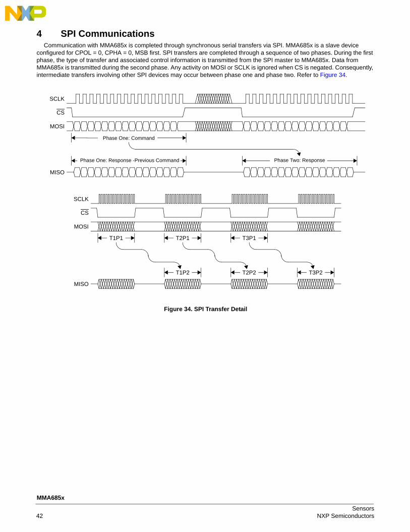
4 SPI CommunicationsCommunication with MMA685x is completed through synchronous serial transfers via SPI. MMA685x is a slave device
configured for CPOL = 0, CPHA = 0, MSB first. SPI transfers are completed through a sequence of two phases. During the first phase, the type of transfer and associated control information is transmitted from the SPI master to MMA685x. Data from MMA685x is transmitted during the second phase. Any activity on MOSI or SCLK is ignored when CS is negated. Consequently, intermediate transfers involving other SPI devices may occur between phase one and phase two. Refer to Figure 34.
Figure 34. SPI Transfer Detail
T3P1
SCLK
MOSI
MISO
CS
T1P1 T2P1
T1P2 T2P2 T3P2
SCLK
MOSI
MISO
CS
Phase One: Command
Phase Two: ResponsePhase One: Response -Previous Command
Sensors42 NXP Semiconductors
MMA685x
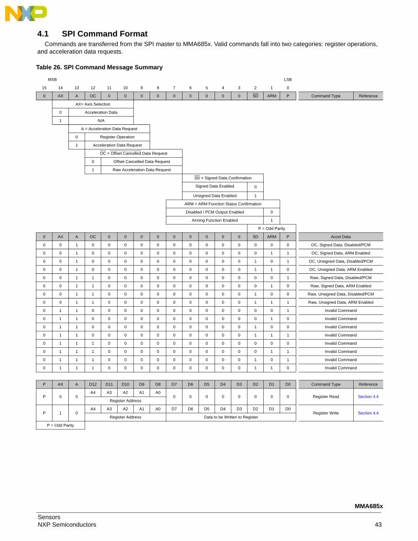
4.1 SPI Command FormatCommands are transferred from the SPI master to MMA685x. Valid commands fall into two categories: register operations,
and acceleration data requests.
Table 26. SPI Command Message Summary
MSB LSB
15 14 13 12 11 10 9 8 7 6 5 4 3 2 1 0
0 AX A OC 0 0 0 0 0 0 0 0 0 SD ARM P Command Type Reference
AX= Axis Selection
0 Acceleration Data
1 N/A
A = Acceleration Data Request
0 Register Operation
1 Acceleration Data Request
OC = Offset Cancelled Data Request
0 Offset Cancelled Data Request
1 Raw Acceleration Data Request
SD = Signed Data Confirmation
Signed Data Enabled 0
Unsigned Data Enabled 1
ARM = ARM Function Status Confirmation
Disabled / PCM Output Enabled 0
Arming Function Enabled 1
P = Odd Parity
0 AX A OC 0 0 0 0 0 0 0 0 0 SD ARM P Accel Data
0 0 1 0 0 0 0 0 0 0 0 0 0 0 0 0 OC, Signed Data, Disabled/PCM
0 0 1 0 0 0 0 0 0 0 0 0 0 0 1 1 OC, Signed Data, ARM Enabled
0 0 1 0 0 0 0 0 0 0 0 0 0 1 0 1 OC, Unsigned Data, Disabled/PCM
0 0 1 0 0 0 0 0 0 0 0 0 0 1 1 0 OC, Unsigned Data, ARM Enabled
0 0 1 1 0 0 0 0 0 0 0 0 0 0 0 1 Raw, Signed Data, Disabled/PCM
0 0 1 1 0 0 0 0 0 0 0 0 0 0 1 0 Raw, Signed Data, ARM Enabled
0 0 1 1 0 0 0 0 0 0 0 0 0 1 0 0 Raw, Unsigned Data, Disabled/PCM
0 0 1 1 0 0 0 0 0 0 0 0 0 1 1 1 Raw, Unsigned Data, ARM Enabled
0 1 1 0 0 0 0 0 0 0 0 0 0 0 0 1 Invalid Command
0 1 1 0 0 0 0 0 0 0 0 0 0 0 1 0 Invalid Command
0 1 1 0 0 0 0 0 0 0 0 0 0 1 0 0 Invalid Command
0 1 1 0 0 0 0 0 0 0 0 0 0 1 1 1 Invalid Command
0 1 1 1 0 0 0 0 0 0 0 0 0 0 0 0 Invalid Command
0 1 1 1 0 0 0 0 0 0 0 0 0 0 1 1 Invalid Command
0 1 1 1 0 0 0 0 0 0 0 0 0 1 0 1 Invalid Command
0 1 1 1 0 0 0 0 0 0 0 0 0 1 1 0 Invalid Command
P AX A D12 D11 D10 D9 D8 D7 D6 D5 D4 D3 D2 D1 D0 Command Type Reference
P 0 0A4 A3 A2 A1 A0
0 0 0 0 0 0 0 0 Register Read Section 4.4Register Address
P 1 0A4 A3 A2 A1 A0 D7 D6 D5 D4 D3 D2 D1 D0
Register Write Section 4.4Register Address Data to be Written to Register
P = Odd Parity
SensorsNXP Semiconductors 43
MMA685x
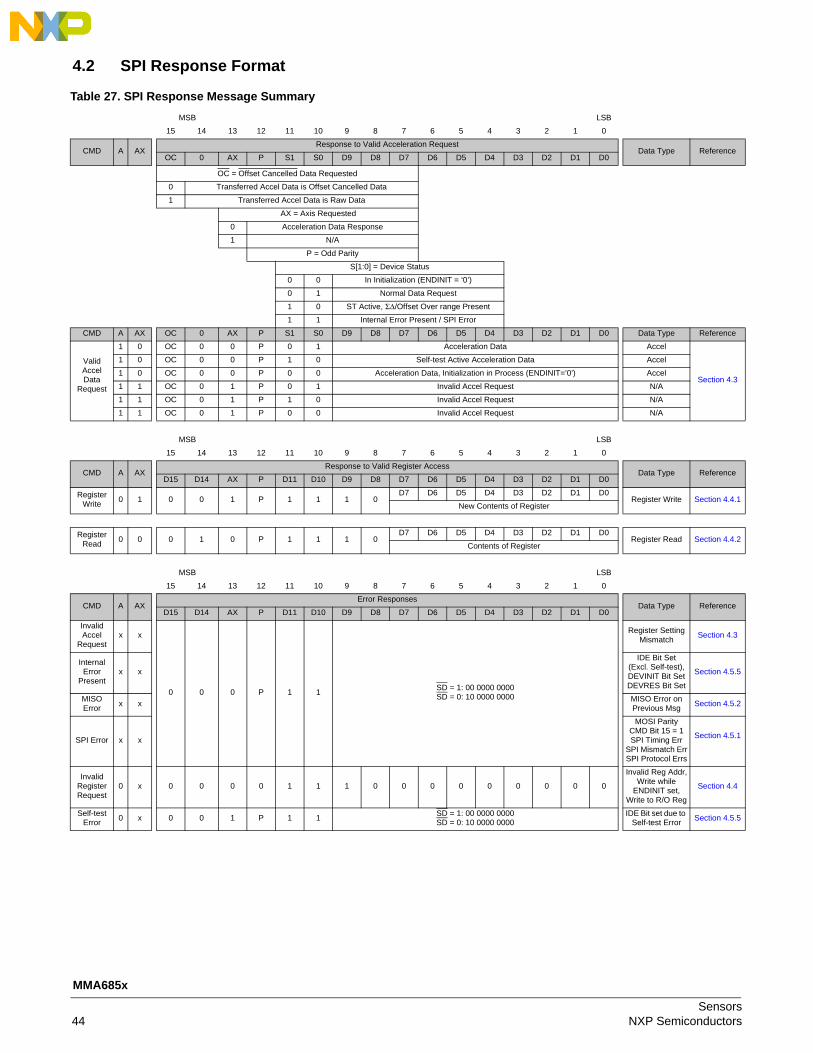
4.2 SPI Response Format
Table 27. SPI Response Message Summary
MSB LSB
15 14 13 12 11 10 9 8 7 6 5 4 3 2 1 0
CMD A AXResponse to Valid Acceleration Request
Data Type ReferenceOC 0 AX P S1 S0 D9 D8 D7 D6 D5 D4 D3 D2 D1 D0
OC = Offset Cancelled Data Requested
0 Transferred Accel Data is Offset Cancelled Data
1 Transferred Accel Data is Raw Data
AX = Axis Requested
0 Acceleration Data Response
1 N/A
P = Odd Parity
S[1:0] = Device Status
0 0 In Initialization (ENDINIT = ‘0’)
0 1 Normal Data Request
1 0 ST Active, ΣΔ/Offset Over range Present
1 1 Internal Error Present / SPI Error
CMD A AX OC 0 AX P S1 S0 D9 D8 D7 D6 D5 D4 D3 D2 D1 D0 Data Type Reference
Valid Accel Data
Request
1 0 OC 0 0 P 0 1 Acceleration Data Accel
Section 4.3
1 0 OC 0 0 P 1 0 Self-test Active Acceleration Data Accel
1 0 OC 0 0 P 0 0 Acceleration Data, Initialization in Process (ENDINIT=’0’) Accel
1 1 OC 0 1 P 0 1 Invalid Accel Request N/A
1 1 OC 0 1 P 1 0 Invalid Accel Request N/A
1 1 OC 0 1 P 0 0 Invalid Accel Request N/A
MSB LSB
15 14 13 12 11 10 9 8 7 6 5 4 3 2 1 0
CMD A AXResponse to Valid Register Access
Data Type ReferenceD15 D14 AX P D11 D10 D9 D8 D7 D6 D5 D4 D3 D2 D1 D0
Register Write
0 1 0 0 1 P 1 1 1 0D7 D6 D5 D4 D3 D2 D1 D0
Register Write Section 4.4.1New Contents of Register
Register Read
0 0 0 1 0 P 1 1 1 0D7 D6 D5 D4 D3 D2 D1 D0
Register Read Section 4.4.2Contents of Register
MSB LSB
15 14 13 12 11 10 9 8 7 6 5 4 3 2 1 0
CMD A AXError Responses
Data Type ReferenceD15 D14 AX P D11 D10 D9 D8 D7 D6 D5 D4 D3 D2 D1 D0
Invalid Accel
Requestx x
0 0 0 P 1 1SD = 1: 00 0000 0000SD = 0: 10 0000 0000
Register SettingMismatch
Section 4.3
Internal Error
Presentx x
IDE Bit Set(Excl. Self-test),DEVINIT Bit SetDEVRES Bit Set
Section 4.5.5
MISO Error
x xMISO Error on Previous Msg
Section 4.5.2
SPI Error x x
MOSI Parity CMD Bit 15 = 1SPI Timing Err
SPI Mismatch ErrSPI Protocol Errs
Section 4.5.1
InvalidRegister Request
0 x 0 0 0 0 1 1 1 0 0 0 0 0 0 0 0 0
Invalid Reg Addr,Write while
ENDINIT set,Write to R/O Reg
Section 4.4
Self-test Error
0 x 0 0 1 P 1 1SD = 1: 00 0000 0000SD = 0: 10 0000 0000
IDE Bit set due to Self-test Error
Section 4.5.5
Sensors44 NXP Semiconductors
MMA685x
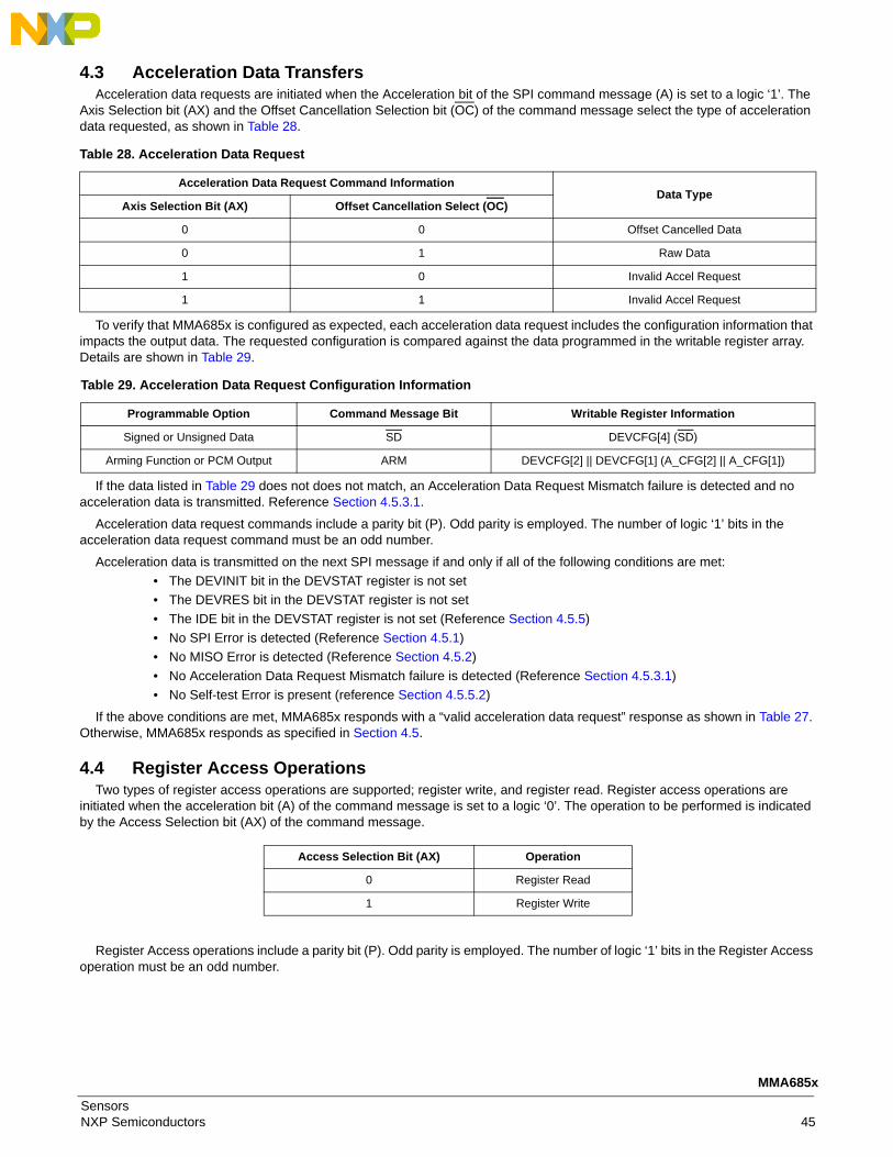
4.3 Acceleration Data TransfersAcceleration data requests are initiated when the Acceleration bit of the SPI command message (A) is set to a logic ‘1’. The
Axis Selection bit (AX) and the Offset Cancellation Selection bit (OC) of the command message select the type of acceleration data requested, as shown in Table 28.
To verify that MMA685x is configured as expected, each acceleration data request includes the configuration information that impacts the output data. The requested configuration is compared against the data programmed in the writable register array. Details are shown in Table 29.
If the data listed in Table 29 does not does not match, an Acceleration Data Request Mismatch failure is detected and no acceleration data is transmitted. Reference Section 4.5.3.1.
Acceleration data request commands include a parity bit (P). Odd parity is employed. The number of logic ‘1’ bits in the acceleration data request command must be an odd number.
Acceleration data is transmitted on the next SPI message if and only if all of the following conditions are met:
• The DEVINIT bit in the DEVSTAT register is not set
• The DEVRES bit in the DEVSTAT register is not set
• The IDE bit in the DEVSTAT register is not set (Reference Section 4.5.5)
• No SPI Error is detected (Reference Section 4.5.1)
• No MISO Error is detected (Reference Section 4.5.2)
• No Acceleration Data Request Mismatch failure is detected (Reference Section 4.5.3.1)
• No Self-test Error is present (reference Section 4.5.5.2)
If the above conditions are met, MMA685x responds with a “valid acceleration data request” response as shown in Table 27. Otherwise, MMA685x responds as specified in Section 4.5.
4.4 Register Access OperationsTwo types of register access operations are supported; register write, and register read. Register access operations are
initiated when the acceleration bit (A) of the command message is set to a logic ‘0’. The operation to be performed is indicated by the Access Selection bit (AX) of the command message.
Register Access operations include a parity bit (P). Odd parity is employed. The number of logic ‘1’ bits in the Register Access operation must be an odd number.
Table 28. Acceleration Data Request
Acceleration Data Request Command InformationData Type
Axis Selection Bit (AX) Offset Cancellation Select (OC)
0 0 Offset Cancelled Data
0 1 Raw Data
1 0 Invalid Accel Request
1 1 Invalid Accel Request
Table 29. Acceleration Data Request Configuration Information
Programmable Option Command Message Bit Writable Register Information
Signed or Unsigned Data SD DEVCFG[4] (SD)
Arming Function or PCM Output ARM DEVCFG[2] || DEVCFG[1] (A_CFG[2] || A_CFG[1])
Access Selection Bit (AX) Operation
0 Register Read
1 Register Write
SensorsNXP Semiconductors 45
MMA685x

4.4.1 Register Write RequestDuring a register write request, bits 12 through 8 contain a 5-bit address, and bits 7 through 0 contain the data value to be
written. Writable registers are defined in Table 3.
The response to a register write operation is shown in Table 27. The response is transmitted on the next SPI message if and only if all of the following conditions are met:
• No SPI Error is detected (Reference Section 4.5.1)
• No MISO Error is detected (Reference Section 4.5.2)
• The ENDINIT bit is cleared (Reference Section 3.1.6.2)
– This applies to all registers with the exception of the DEVCTL register
• No Invalid Register Request is detected (Reference Section 4.5.3.2)
If the above conditions are met, MMA685x responds to the register write request as shown in Table 27. Otherwise, MMA685x responds as specified in Section 4.5.
Register write operations do not occur internally until the transfer during which they are requested has been completed. In the event that a SPI Error is detected during a register write transfer, the write operation is not completed.
4.4.2 Register Read RequestDuring a register read request, bits 12 through 8 contain the 5-bit address for the register to be read. Bits 7 through 0 must be
logic ‘0’. Readable registers are defined in Table 3.
The response to a register read operation is shown in Table 27. The response is transmitted on the next SPI message if and only if all of the following conditions are met:
• No SPI Error is detected (Reference Section 4.5.1)
• No MISO Error is detected (Reference Section 4.5.2)
• No Invalid Register Request is detected (Reference Section 4.5.3.2)
If the above conditions are met, MMA685x responds to the register read request as shown in Table 27. Otherwise, MMA685x responds as specified in Section 4.5.
4.5 Exception HandlingThe following sections describe the conditions for each detectable exception, and the MMA685x response for each exception.
In the event that multiple exceptions exist, the exception response is determined by the priority listed in Table 30.
Table 30. SPI Error Response Priority
Error Priority ExceptionEffect on Data
SPI Data Arming Output PCM Output
1 SPI Error Error Response No Update No Effect
2 SPI MISO Error Error Response No Update No Effect
3 Invalid Request Error Response No Update No Effect
4 DEVINIT Bit Set Error Response No Update Disabled
5 DEVRES Error Error Response No Update Disabled
6 CRC Error Error Response No Update No Effect
7 Self-test Error Error Response No Update No Effect
8 Offset Monitor Over Range No Effect No Effect No Effect
9 ΣΔ Over Range No Effect No Effect No Effect
Sensors46 NXP Semiconductors
MMA685x
4.5.1 SPI ErrorThe following SPI conditions result in a SPI error:
• SCLK is high when CS is asserted
• the number of SCLK rising edges detected while CS is asserted is not equal to 16
• SCLK is high when CS is negated
• Command message parity error (MOSI)
• Bit 15 of Acceleration Data Request is not equal to ‘0’
• Bits 3 through 11 of an Acceleration Request are not equal to ‘0’
• Bits 0 through 7 of a Register Read Request are not equal to ‘0’
MMA685x responds to a SPI error with a “SPI Error” response as shown in Table 27. This applies to both acceleration data request SPI errors, and Register Access SPI errors.
The arming function will not be updated if a SPI Error is detected. The PCM output is not affected by a SPI Error.
4.5.2 SPI Data Output Verification ErrorMMA685x includes a function to verify the integrity of the data output to the MISO pin. The function reads the data transmitted
on the MISO pin and compares it against the data intended to be transmitted. If any one bit doesn’t match, a SPI MISO Mismatch Fault is detected and the MISOERR flag in the DEVSTAT register is set.
If a valid SPI acceleration request message is received during the SPI transfer with the MISO mismatch failure, the SPI acceleration request message is ignored and MMA685x responds with a “MISO Error” response during the subsequent SPI message (reference Table 27). The Arming function is not updated if a MISO mismatch failure occurs. The PCM function is not affected by the MISO mismatch failure.
If a valid SPI register write request message is received during the SPI transfer with the MISO mismatch failure, the register write is completed as requested, but MMA685x responds with a “MISO Error” response as shown in Table 27, during the subsequent SPI message.
If a valid SPI register read request message is received during the SPI transfer with the MISO mismatch failure, the register read is ignored and MMA685x responds with a “MISO Error” response as shown in Table 27, during the subsequent SPI message. If the register read request is for the DEVSTAT register, the DEVSTAT register will not be cleared.
In all cases, the MISOERR flag in the DEVSTAT register will remain set until a successful SPI Register Read Request of the DEVSTAT register is completed.
Figure 35. SPI Data Output Verification
4.5.3 Invalid Requests
4.5.3.1 Invalid Acceleration RequestThe following conditions result in an “Invalid Acceleration Request” error:
• The Axis Selection bit (AX) in the Command message is set
• The SPI “Acceleration Data Request” Command data listed in Section 4.3, Table 29 does not match the internal register settings
MMA685x responds to an “Invalid Acceleration Request” error with an “Invalid Accel Request” response as specified in Table 27 on the subsequent SPI message only. No internal fault is recorded. The arming function will not be updated if an “Acceleration Data Request Mismatch” Error is detected. The PCM output is not affected by the “Acceleration Data Request Mismatch” error.
Register operations will be executed as specified in Section 4.4.
D Q
R
D Q
R
D Q
SCLK
SPI DATA OUT SHIFT REGISTER DATA OUT BUFFER
MISO
MISO ERR
SensorsNXP Semiconductors 47
MMA685x

4.5.3.2 Invalid Register RequestThe following conditions result in an “Invalid Register Request” error:
• An attempt is made to write to an un-writable register (Writable registers are defined in Section 3.1, Table 3). Attempts to write to registers $0D, $0F, $11, and $13 will also result in an error.
• An attempt is made to write to a register while the ENDINIT bit in the DEVCFG register is set
– This applies to all registers with the exception of the DEVCTL register
• An attempt is made to read an un-readable register (Readable registers are defined in Section 3.1, Table 3). Attempts to read registers $07, $0D, $0F, $11, and $13 will also result in an error.
MMA685x responds to an Invalid Register Request” error with an “Invalid Register Request” response as shown in Table 27.
4.5.4 Device Reset IndicationsIf the DEVINIT, or DEVRES bit is set in the DEVSTAT register as described in Section 3.1.10, MMA685x will respond to
acceleration data requests with an “Internal Error Present” response until the bits are cleared in the DEVSTAT register. The DEVINIT bit is cleared automatically when device initialization is complete (Reference tOP in Section 2.6). The DEVRES bit is cleared on a read of the DEVSTAT register. The arming function will not be updated on Acceleration Data Request commands if the DEVINIT or DEVRES bit is set in the DEVSTAT register. The PCM output is disabled if the DEVINIT or DEVRES bit is set.
4.5.5 Internal ErrorThe following errors will result in an internal error, and set the IDE bit in the DEVSTAT register:
• OTP CRC Failure
• Writable Register CRC Failure
• Self-test Error
• Invalid internal logic states
4.5.5.1 CRC ErrorIf the IDE bit is set in the DEVSTAT register due to an OTP Shadow Register or Writable Register CRC failure as described in
Section 3.2, MMA685x will respond to acceleration data requests with an “Internal Error Present” response until the IDE bit is cleared in the DEVSTAT register. The arming function will not be updated on Acceleration Data Request commands if a CRC Error is detected. The PCM output is not affected by the CRC error.
If the CRC error is in the writable register array, and the ENDINIT bit in the DEVCFG register has been set, the error can only be cleared by a device reset. The IDE bit will not be cleared on a read of the DEVSTAT register.
If the CRC error is in the OTP shadow register array, the error cannot be cleared.
Register operations will be executed as specified in Section 4.4.
4.5.5.2 Self-test ErrorIf the IDE bit is set in the DEVSTAT register due to a Self-test activation failure, MMA685x will respond to acceleration data
requests with a “Self-test Error” response until the IDE bit is cleared in the DEVSTAT register. The arming function will not be updated on Acceleration Data Request commands if a Self-test Error is detected. The PCM output is not affected by the Self-test Error. The IDE bit in the DEVSTAT register will remain set until a read of the DEVSTAT register occurs, even if the internal failure is removed. If the internal error is still present when the DEVSTAT register is read, the IDE bit will remain set.
Register operations will be executed as specified in Section 4.4.
4.5.6 Offset Monitor Over Range If an offset monitor over range is present as described in Section 3.8.5, MMA685x will respond to an acceleration request with
a “Valid Acceleration Data Request” response, but the Status bits (S[1:0]) will be set to ‘10’. The arming function will be updated on Acceleration Data Request commands even if an Offset Monitor Over Range is detected. Once the over range condition is removed, MMA685x will respond to acceleration requests with a “Valid Acceleration Data Request” response with the Status bits (S[1:0]) set to ‘10’ on the next SPI transfer, and a “Valid Acceleration Data Request” response with normal status on subsequent SPI transfers. The OFF bit in the DEVSTAT register will remain set until a read of the DEVSTAT register occurs.
The PCM output is not affected by the offset monitor over range condition.
Register operations will be executed as specified in Section 4.4.
Sensors48 NXP Semiconductors
MMA685x
4.5.7 ΣΔ Over RangeIf a ΣΔ Over Range failure is present as described in Section 3.11.2, MMA685x will respond to acceleration data requests with
a “Valid Acceleration Data Request” response, but the Status bits (S[1:0]) will be set to ‘10’. The arming function will be updated on Acceleration Data Request commands even if a ΣΔ Over Range is detected. Once the over range condition is removed, MMA685x will respond to acceleration requests with a “Valid Acceleration Data Request” response with the Status bits (S[1:0]) set to ‘10’ on the next SPI transfer, and a “Valid Acceleration Data Request” response with normal status on subsequent SPI transfers. The SDOV bit in the DEVSTAT register will remain set until a read of the DEVSTAT register occurs.
The PCM output is not affected by the ΣΔ over range condition.
Register operations will be executed as specified in Section 4.4.
4.6 Initialization SPI ResponseThe first data transmitted by MMA685x following reset is the SPI Error response shown in Table 27. This ensures that an
unexpected reset will always be detectable. MMA685x will respond to all acceleration data requests with the “Invalid Acceleration Data Request” response until the DEVRES bit in the DEVSTAT register is cleared via a read of the DEVSTAT register. The arming function will not be updated on Acceleration Data Request commands until the DEVRES bit in the DEVSTAT register is cleared.
4.7 Acceleration Data RepresentationAcceleration values are determined from the 10-bit digital output (DV) using the following equations:
The linear range of digital values for signed data is –480 to +480, and for unsigned data is 32 to 992. Resulting ranges and some nominal acceleration values are shown in Table 31.
Figure 36 shows the how the possible output data codes are determined from the input data and the error sources. The relevant parameters are specified in Section 2.4.
Acceleration SensitivityLSB DV 512–( )×=
Acceleration SensitivityLSB DV×= For Signed Data
For Unsigned Data
Table 31. Nominal Acceleration Data Values
UnsignedDigital Value
SignedDigital Value
Nominal Acceleration
Trimmed forMaximum Sensitivity
(g)
Trimmed forMaximum Range
(g)
993 to 1023 481 to 511 Unused
992 480 19.666 117.19
991 479 19.625 116.94
•••
•••
•••
•••
514 2 +0.082 +0.488
513 1 +0.041 +0.244
512 0 0 0
511 –1 –0.041 –0.244
510 –2 –0.082 –0.488
•••
•••
•••
•••
33 –479 –19.625 –116.94
32 –480 –19.666 –117.19
1 to 31 –481 to –511 Unused
0 –512 Fault
SensorsNXP Semiconductors 49
MMA685x
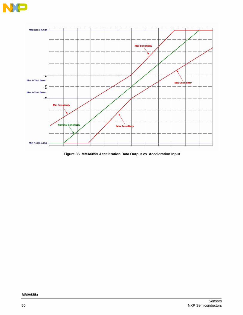
Figure 36. MMA685x Acceleration Data Output vs. Acceleration Input
Sensors50 NXP Semiconductors
MMA685x
5 Package
5.1 Case Outline DrawingReference NXP Case Outline Drawing # 98ASA00690D for the MMA685xBKC part numbers.
http://www.NXP.com/files/shared/doc/package_info/98ASA00690D.pdf
Reference NXP Case Outline Drawing # 98ASA00090D for the MMA685xBKT part numbers.
http://www.NXP.com/files/shared/doc/package_info/98ASA00090D.pdf
5.2 Recommended FootprintReference NXP Application Note AN1902, latest revision:
http://cache.NXP.com/files/analog/doc/app_note/AN1902.pdf
6 Revision History
Table 32. Revision History
Revision number
Revision date
Description of changes
4 12/2011 • Updated ordering table to include Tube options; deleted MMA6852 and MMA6854. • Deleted MMA6852 and MMA6854 devices from Electrical Characteristics table, lines 57 and 60.
Removed “QR2” from device names, lines 56–59. • Updated equation in section 3.6, Self-test Interface.
5 03/2012 • Added SafeAssure logo, changed first paragraph and disclaimer to include trademark information.
6 11/2014 • Changed device numbers in ordering table for location code changes. • Updated Part Marking Diagram. • Changed application note reference from AN3111 to AN1902. • Added additional package for C suffix device options.
7 01/2016 • Changed format to new corporate style.
SensorsNXP Semiconductors 51
MMA685x

Document Number: MMA685xRev. 701/2016
Information in this document is provided solely to enable system and software
implementers to use NXP products. There are no express or implied copyright licenses
granted hereunder to design or fabricate any integrated circuits based on the
information in this document.
NXP reserves the right to make changes without further notice to any products herein.
NXP makes no warranty, representation, or guarantee regarding the suitability of its
products for any particular purpose, nor does NXP assume any liability arising out of
the application or use of any product or circuit, and specifically disclaims any and all
liability, including without limitation consequential or incidental damages. “Typical”
parameters that may be provided in NXP data sheets and/or specifications can and do
vary in different applications, and actual performance may vary over time. All operating
parameters, including “typicals,” must be validated for each customer application by
customer’s technical experts. NXP does not convey any license under its patent rights
nor the rights of others. NXP sells products pursuant to standard terms and conditions
of sale, which can be found at the following address: NXP.com/
salestermsandconditions.
How to Reach Us:
Home Page: NXP.com
Web Support: NXP.com/support
NXP, the NXP logo, Freescale, the Freescale logo, and SafeAssure are trademarks of
NXP B.V. All other product or service names are the property of their respective
owners.
© 2016 NXP B.V.