Embed Size (px)
Citation preview
International Journal of Scientific & Engineering Research, Volume 4, Issue 12, December-2013 119 ISSN 2229-5518
IJSER © 2013 http://www.ijser.org
Modeling and Analysis of Three Phase Varia-ble Load Connected Photo-voltaic System
Sankalp Verma, Shweta Dave and R. N. Patel
Abstract: This paper presents the mathematical modeling of three phase Photovoltaic system con-nected with variable load using MATLAB/Simulink environment. The system consists of a PV Array, Boost converter, three phase inverter and its control to maintain three phase variable load. The 40 kW PV system is studied with a variable inductive load of 30 kW. The paper gives analysis of each component of system. The constant and boosted DC voltage is obtained with the help of boost converter from PV Array. The three phase IGBT inverter PWM control scheme is proposed here to normalize the voltage imbalance during variable load. The PI controller is used to attain maximum active power from inverter and to maintain the reactive power requirements. Keywords: Active Power, Boost Converter, PV Array, PI Controller and Variable Load.
—————————— ——————————
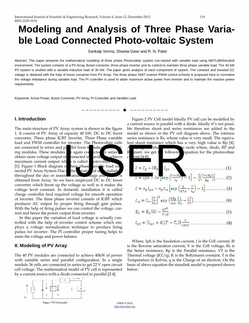
I. Introduction The main structure of PV Array system is shown in the figure 1. It consist of PV Array of capacity 40 kW, DC to DC boost converter, Three phase IGBT Inverter, Three Phase variable load and PWM controller for inverter. The Photovoltaic cells are connected in series and parallel form to make desired rat-ing modules. These modules are again connected in series to obtain more voltage output or connected in parallel to achieve maximum current output which is called Photovoltaic Array [1]. Figure 1 Block diagram of three phase variable load con-nected PV Array System Due to the variation of solar radiation throughout the day or season, variable voltage and power is obtained from Array. So we have employed DC to DC boost converter which boost up the voltage as well as it makes the voltage level constant. In domestic installation it is called charge controller feed required voltage for smooth operation of inverter. The three phase inverter consists of IGBT which produces AC output by proper firing through gate pulses. With the help of firing pulses we can control the voltage, cur-rent and hence the power output from inverter.
In this paper the variation of load voltage is actually con-trolled with the help of inverter control scheme which em-ploys a voltage normalization technique to produce firing pulses for inverter. The PI controller proper tuning helps to main the voltage and power balance
II. Modeling of PV Array
The 40 PV modules are connected to achieve 40kW of power with suitable series and parallel configuration. In a single module 36 cells are connected in series to get 22 V open circuit cell voltage. The mathematical model of PV cell is represented by a current source with a diode connected in parallel [2-4].
Figure 2 PV Cell model Ideally PV cell can be modelled by a current source in parallel with a diode. Ideally it‟s not possi-ble therefore shunt and series resistances are added to the model as shown in the PV cell diagram above. The intrinsic series resistance is Rs, whose value is very small. The equiva-lent shunt resistance which has a very high value is Rp [4]. Applying Kirchhoff‟s law to the node where, diode, RP and RS meet, we get the following equation for the photovoltaic current [4-8]:
Where, Iph is the Insolation current, I is the Cell current, I0
is the Reverse saturation current, V is the Cell voltage, Rs is the Series resistance, Rp is the Parallel resistance, VT is the Thermal voltage (KT/q), K is the Boltzmann constant, T is the Temperature in Kelvin, q is the Charge of an electron. On the basis of above equation the simulink model is prepared shown below:
IJSER
International Journal of Scientific & Engineering Research, Volume 4, Issue 12, December-2013 120 ISSN 2229-5518
IJSER © 2013 http://www.ijser.org
III. Boost Converter
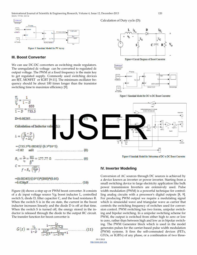
We can use DC-DC converters as switching mode regulators. The unregulated dc voltage can be converted to regulated dc output voltage. The PWM at a fixed frequency is the main key to get regulated supply. Commonly used switching devices are BJT, MOSFET or IGBT [9-11]. The minimum oscillator fre-quency should be about 100 times longer than the transistor switching time to maximize efficiency [9].
Calculation of Duty cycle (D):
Figure (4) shows a step up or PWM boost converter. It consists of a dc input voltage source Vg; boost inductor L, controlled switch S, diode D, filter capacitor C, and the load resistance R. When the switch S is in the on state, the current in the boost inductor increases linearly and the diode D is off at that time. When the switch S is turned off, the energy stored in the in-ductor is released through the diode to the output RC circuit. The transfer function for boost converter is
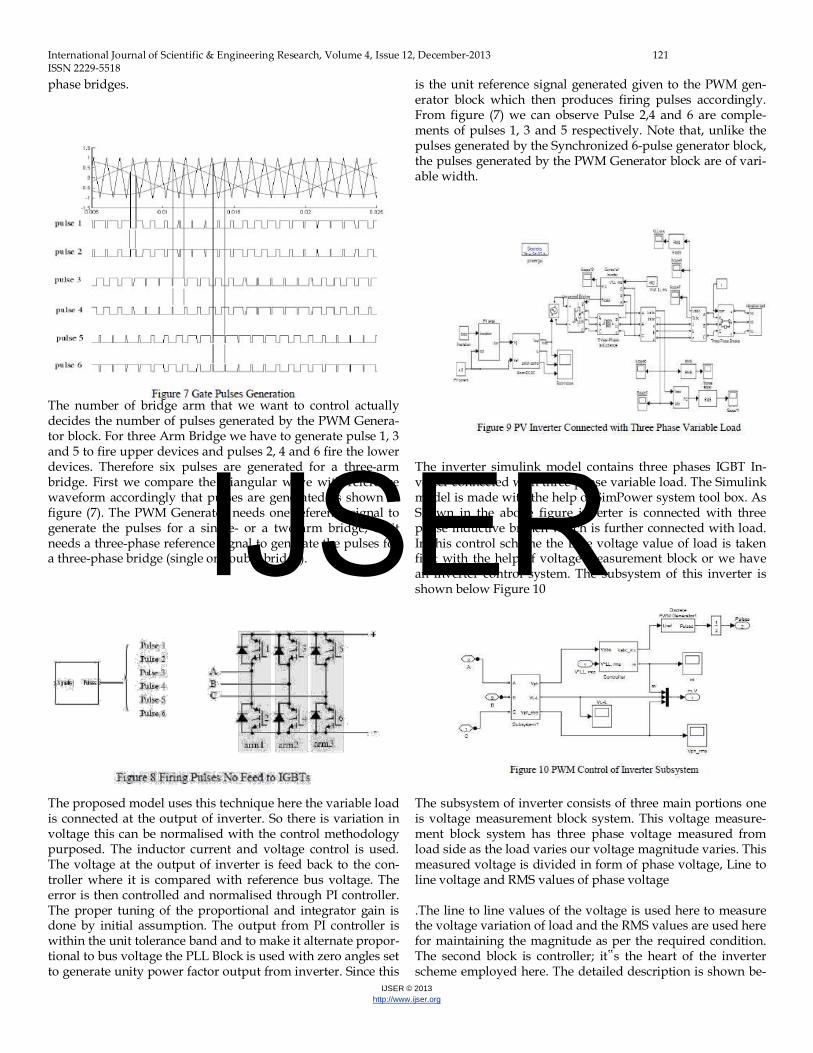
IV. Inverter Modeling Conversion of AC sources through DC sources is achieved by a device known as inverter or power inverter. Starting from a small switching device to large electricity application like bulk power transmission Inverters are extensively used. Pulse width modulation (PWM) is a powerful technique for control-ling analog circuits with a processor's digital outputs [8, 9]. For producing PWM output we require a modulating signal which is sinusoidal wave and triangular wave as carrier that controls the switching frequency of switches used for conver-sion control. PWM switching has two forms, unipolar switch-ing and bipolar switching. In a unipolar switching scheme for PWM, the output is switched from either high to zero or low to zero, rather than between high and low as in bipolar switch-ing. The PWM Generator block which is used in the model generates pulses for the carrier-based pulse width modulation (PWM) systems. It fires the self-commuted devices (FETs, GTOs, or IGBTs) of any phase, or a combination of two three-
IJSER
International Journal of Scientific & Engineering Research, Volume 4, Issue 12, December-2013 121 ISSN 2229-5518
IJSER © 2013 http://www.ijser.org
phase bridges. The number of bridge arm that we want to control actually decides the number of pulses generated by the PWM Genera-tor block. For three Arm Bridge we have to generate pulse 1, 3 and 5 to fire upper devices and pulses 2, 4 and 6 fire the lower devices. Therefore six pulses are generated for a three-arm bridge. First we compare the triangular wave with reference waveform accordingly that pulses are generated as shown in figure (7). The PWM Generator needs one reference signal to generate the pulses for a single- or a two-arm bridge, or it needs a three-phase reference signal to generate the pulses for a three-phase bridge (single or double bridge). The proposed model uses this technique here the variable load is connected at the output of inverter. So there is variation in voltage this can be normalised with the control methodology purposed. The inductor current and voltage control is used. The voltage at the output of inverter is feed back to the con-troller where it is compared with reference bus voltage. The error is then controlled and normalised through PI controller. The proper tuning of the proportional and integrator gain is done by initial assumption. The output from PI controller is within the unit tolerance band and to make it alternate propor-tional to bus voltage the PLL Block is used with zero angles set to generate unity power factor output from inverter. Since this
is the unit reference signal generated given to the PWM gen-erator block which then produces firing pulses accordingly. From figure (7) we can observe Pulse 2,4 and 6 are comple-ments of pulses 1, 3 and 5 respectively. Note that, unlike the pulses generated by the Synchronized 6-pulse generator block, the pulses generated by the PWM Generator block are of vari-able width. The inverter simulink model contains three phases IGBT In-verter connected with three phase variable load. The Simulink model is made with the help of SimPower system tool box. As Shown in the above figure inverter is connected with three phase inductive branch which is further connected with load. In this control scheme the Line voltage value of load is taken first with the help of voltage measurement block or we have an inverter control system. The subsystem of this inverter is shown below Figure 10 The subsystem of inverter consists of three main portions one is voltage measurement block system. This voltage measure-ment block system has three phase voltage measured from load side as the load varies our voltage magnitude varies. This measured voltage is divided in form of phase voltage, Line to line voltage and RMS values of phase voltage .The line to line values of the voltage is used here to measure the voltage variation of load and the RMS values are used here for maintaining the magnitude as per the required condition. The second block is controller; it‟s the heart of the inverter scheme employed here. The detailed description is shown be-
IJSER
International Journal of Scientific & Engineering Research, Volume 4, Issue 12, December-2013 122 ISSN 2229-5518
IJSER © 2013 http://www.ijser.org
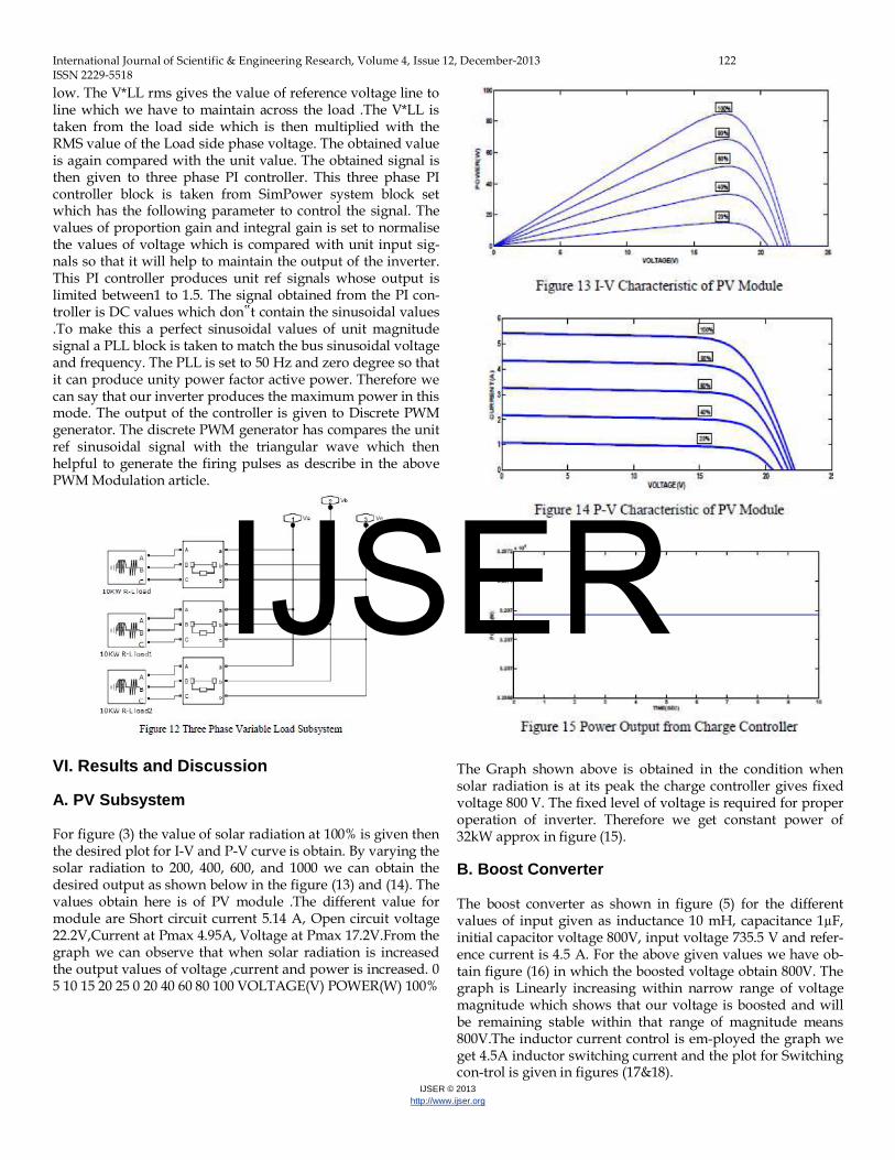
low. The V*LL rms gives the value of reference voltage line to line which we have to maintain across the load .The V*LL is taken from the load side which is then multiplied with the RMS value of the Load side phase voltage. The obtained value is again compared with the unit value. The obtained signal is then given to three phase PI controller. This three phase PI controller block is taken from SimPower system block set which has the following parameter to control the signal. The values of proportion gain and integral gain is set to normalise the values of voltage which is compared with unit input sig-nals so that it will help to maintain the output of the inverter. This PI controller produces unit ref signals whose output is limited between1 to 1.5. The signal obtained from the PI con-troller is DC values which don‟t contain the sinusoidal values .To make this a perfect sinusoidal values of unit magnitude signal a PLL block is taken to match the bus sinusoidal voltage and frequency. The PLL is set to 50 Hz and zero degree so that it can produce unity power factor active power. Therefore we can say that our inverter produces the maximum power in this mode. The output of the controller is given to Discrete PWM generator. The discrete PWM generator has compares the unit ref sinusoidal signal with the triangular wave which then helpful to generate the firing pulses as describe in the above PWM Modulation article. VI. Results and Discussion A. PV Subsystem For figure (3) the value of solar radiation at 100% is given then the desired plot for I-V and P-V curve is obtain. By varying the solar radiation to 200, 400, 600, and 1000 we can obtain the desired output as shown below in the figure (13) and (14). The values obtain here is of PV module .The different value for module are Short circuit current 5.14 A, Open circuit voltage 22.2V,Current at Pmax 4.95A, Voltage at Pmax 17.2V.From the graph we can observe that when solar radiation is increased the output values of voltage ,current and power is increased. 0 5 10 15 20 25 0 20 40 60 80 100 VOLTAGE(V) POWER(W) 100%
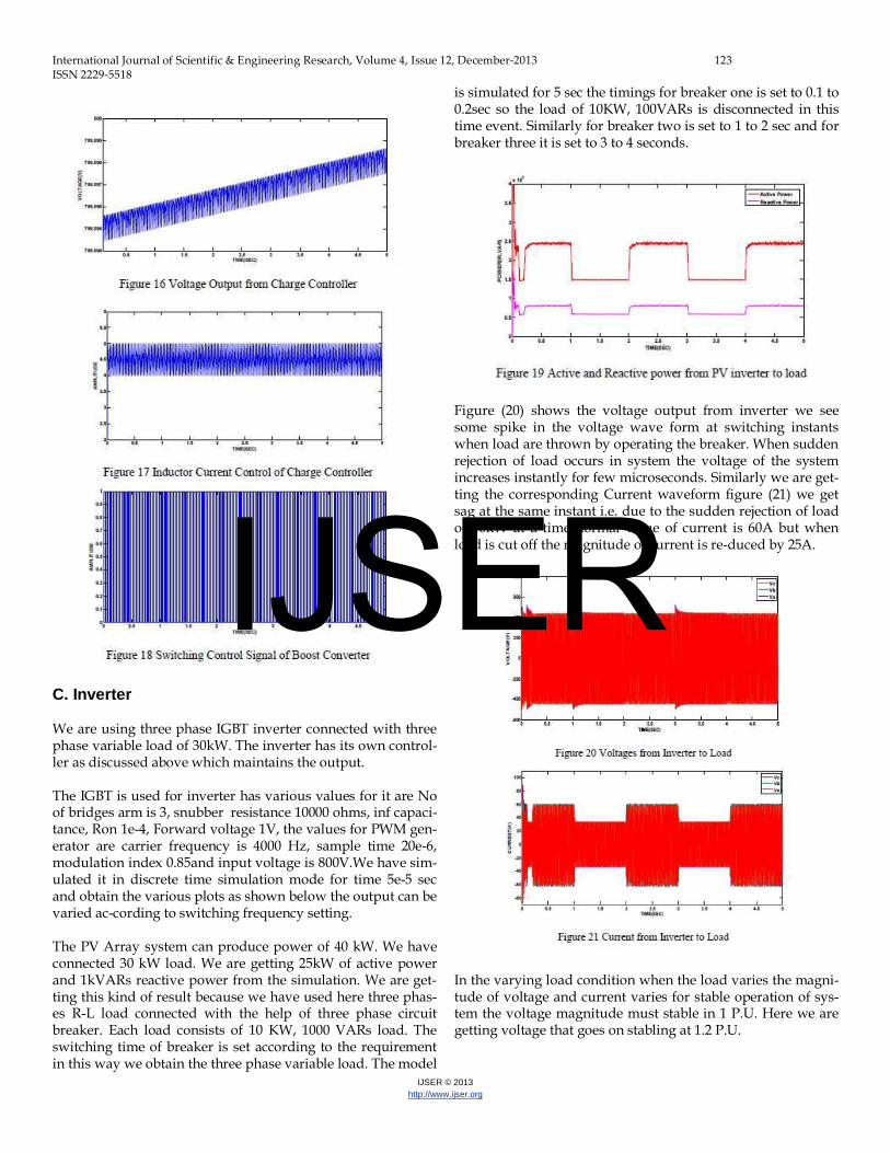
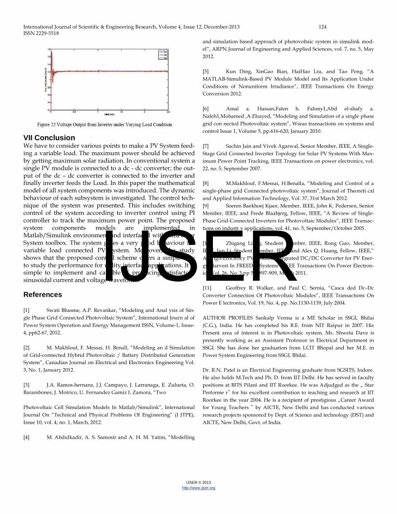
The Graph shown above is obtained in the condition when solar radiation is at its peak the charge controller gives fixed voltage 800 V. The fixed level of voltage is required for proper operation of inverter. Therefore we get constant power of 32kW approx in figure (15). B. Boost Converter The boost converter as shown in figure (5) for the different values of input given as inductance 10 mH, capacitance 1µF, initial capacitor voltage 800V, input voltage 735.5 V and refer-ence current is 4.5 A. For the above given values we have ob-tain figure (16) in which the boosted voltage obtain 800V. The graph is Linearly increasing within narrow range of voltage magnitude which shows that our voltage is boosted and will be remaining stable within that range of magnitude means 800V.The inductor current control is em-ployed the graph we get 4.5A inductor switching current and the plot for Switching con-trol is given in figures (17&18).
IJSER
International Journal of Scientific & Engineering Research, Volume 4, Issue 12, December-2013 123 ISSN 2229-5518
IJSER © 2013 http://www.ijser.org
C. Inverter We are using three phase IGBT inverter connected with three phase variable load of 30kW. The inverter has its own control-ler as discussed above which maintains the output. The IGBT is used for inverter has various values for it are No of bridges arm is 3, snubber resistance 10000 ohms, inf capaci-tance, Ron 1e-4, Forward voltage 1V, the values for PWM gen-erator are carrier frequency is 4000 Hz, sample time 20e-6, modulation index 0.85and input voltage is 800V.We have sim-ulated it in discrete time simulation mode for time 5e-5 sec and obtain the various plots as shown below the output can be varied ac-cording to switching frequency setting. The PV Array system can produce power of 40 kW. We have connected 30 kW load. We are getting 25kW of active power and 1kVARs reactive power from the simulation. We are get-ting this kind of result because we have used here three phas-es R-L load connected with the help of three phase circuit breaker. Each load consists of 10 KW, 1000 VARs load. The switching time of breaker is set according to the requirement in this way we obtain the three phase variable load. The model
is simulated for 5 sec the timings for breaker one is set to 0.1 to 0.2sec so the load of 10KW, 100VARs is disconnected in this time event. Similarly for breaker two is set to 1 to 2 sec and for breaker three it is set to 3 to 4 seconds. Figure (20) shows the voltage output from inverter we see some spike in the voltage wave form at switching instants when load are thrown by operating the breaker. When sudden rejection of load occurs in system the voltage of the system increases instantly for few microseconds. Similarly we are get-ting the corresponding Current waveform figure (21) we get sag at the same instant i.e. due to the sudden rejection of load of 10kW at a time normal value of current is 60A but when load is cut off the magnitude of current is re-duced by 25A. In the varying load condition when the load varies the magni-tude of voltage and current varies for stable operation of sys-tem the voltage magnitude must stable in 1 P.U. Here we are getting voltage that goes on stabling at 1.2 P.U.
IJSER
International Journal of Scientific & Engineering Research, Volume 4, Issue 12, December-2013 124 ISSN 2229-5518
IJSER © 2013 http://www.ijser.org
VII Conclusion We have to consider various points to make a PV System feed-ing a variable load. The maximum power should be achieved by getting maximum solar radiation. In conventional system a single PV module is connected to a dc - dc converter; the out-put of the dc – dc converter is connected to the inverter and finally inverter feeds the Load. In this paper the mathematical model of all system components was introduced. The dynamic behaviour of each subsystem is investigated. The control tech-nique of the system was presented. This includes switching control of the system according to inverter control using PI controller to track the maximum power point. The proposed system components models are implemented in Matlab/Simulink environment and interfaced with SimPower System toolbox. The system gives a very good behaviour for variable load connected PV system. Moreover, the study shows that the proposed control scheme offers a simple way to study the performance for utility interface applications. It is simple to implement and capable of producing satisfactory sinusoidal current and voltage waveforms. References [1] Swati Bhasme, A.P. Revankar, “Modeling and Anal ysis of Sin-gle Phase Grid Connected Photovoltaic System”, International Journ al of Power System Operation and Energy Management ISSN, Volume-1, Issue-4, pp62-67, 2012. [2] M. Makhlouf, F. Messai, H. Benall, “Modeling an d Simulation of Grid-connected Hybrid Photovoltaic / Battery Distributed Generation System”, Canadian Journal on Electrical and Electronics Engineering Vol. 3, No. 1, January 2012. [3] J.A. Ramos-hernanz, J.J. Campayo, J. Larranaga, E. Zulueta, O. Barambones, J. Motrico, U. Fernandez Gamiz I. Zamora, “Two Photovoltaic Cell Simulation Models In Matlab/Simulink”, International Journal On “Technical and Physical Problems Of Engineering” (I JTPE), Issue 10, vol. 4, no. 1, March, 2012. [4] M. Abdulkadir, A. S. Samosir and A. H. M. Yatim, “Modelling
and simulation based approach of photovoltaic system in simulink mod-el”, ARPN Journal of Engineering and Applied Sciences, vol. 7, no. 5, May 2012. [5] Kun Ding, XinGao Bian, HaiHao Liu, and Tao Peng, “A MATLAB-Simulink-Based PV Module Model and Its Application Under Conditions of Nonuniform Irradiance”, IEEE Transactions On Energy Conversion 2012. [6] Amal a. Hassan,Faten h. Fahmy1,Abd el-shafy a. Nafeh1,Mohamed ,A.Elsayed, “Modeling and Simulation of a single phase grid con nected Photovoltaic system”, Wseas transactions on systems and control Issue 1, Volume 5, pp.616-620, January 2010. [7] Sachin Jain and Vivek Agarwal, Senior Member, IEEE, A Single- Stage Grid Connected Inverter Topology for Solar PV Systems With Max-imum Power Point Tracking, IEEE Transactions on power electronics, vol. 22, no. 5, September 2007. [8] M.Makhlouf, F.Messai, H.Benalla, “Modeling and Control of a single-phase grid Connected photovoltaic system”, Journal of Theoreti cal and Applied Information Technology, Vol. 37, 31st March 2012. [9] Soeren Baekhoej Kjaer, Member, IEEE, John K. Pedersen, Senior Member, IEEE, and Frede Blaabjerg, Fellow, IEEE, “A Review of Single- Phase Grid-Connected Inverters for Photovoltaic Modules”, IEEE Transac-tions on industr y applications, vol. 41, no. 5, September/October 2005. [10] Zhigang Liang, Student Member, IEEE, Rong Guo, Member, IEEE, Jun Li, Student Member, IEEE, and Alex Q. Huang, Fellow, IEEE,” A H igh-Efficiency PV Module-Integrated DC/DC Converter for PV Ener-gy Harvest In FREEDM Systems”, IEEE Transactions On Power Electron-ics, Vol. 26, No. 3,pp No.897-909, March 2011. [11] Geoffrey R. Walker, and Paul C. Sernia, “Casca ded Dc–Dc Converter Connection Of Photovoltaic Modules”, IEEE Transactions On Power E lectronics, Vol. 19, No. 4, pp. No.1130-1139, July 2004. AUTHOR PROFILES Sankalp Verma is a ME Scholar in SSGI, Bhilai (C.G.), India. He has completed his B.E. from NIT Raipur in 2007. His Present area of interest is in Photovoltaic system. Ms. Shweta Dave is presently working as an Assistant Professor in Electrical Department in SSGI. She has done her graduation from LCIT Bhopal and her M.E. in Power System Engineering from SSGI, Bhilai. Dr. R.N. Patel is an Electrical Engineering graduate from SGSITS, Indore. He also holds M.Tech and Ph. D. from IIT Delhi. He has served in faculty positions at BITS Pilani and IIT Roorkee. He was Adjudged as the „ Star Performe r‟ for his excellent contribution to teaching and research at IIT Roorkee in the year 2004. He is a recipient of prestigious „Career Award for Young Teachers ‟ by AICTE, New Delhi and has conducted various research projects sponsored by Dept. of Science and technology (DST) and AICTE, New Delhi, Govt. of India.
IJSER


![CS Amplifier With Diode Connected Load 020303[1]](https://img.pdfslide.net/doc/110x75/54776811b4af9f96108b47bf/cs-amplifier-with-diode-connected-load-0203031.jpg)