Embed Size (px)
Citation preview
DEGREE PROJECT, IN ,MICROELECTRONICS AND APPLIED PHYSICS IT161XFIRST LEVEL
STOCKHOLM, SWEDEN 2014
Modeling of KTH UTBSOI MOSFET
MAX CHUAN CHEN
KTH ROYAL INSTITUTE OF TECHNOLOGY
KTH SCHOOL OF INFOMATION AND COMMUNICATION TECHNOLOGY

Modeling of
KTH UTBSOI MOSFET
by
Max Chuan Chen
A bachelor thesis submitted in fulfillment of the requirements for the degree of Bachelor of Science in
Engineering - Microelectronics
written at
Department of Integrated Devices and Circuits, School of Information and Communication Technology,
Royal Institute of Technology, Stockholm
Thesis Supervisor: Doc. Per-Erik Hellström
KTH Department of Integrated Devices and Circuits
Thesis Examiner: Prof. B Gunnar Malm
KTH Department of Integrated Devices and Circuits
November 2014 Stockholm

i
Abstract Semiconductor devices such as transistors and integrated circuits are everywhere in our daily lives, it's one of the most important foundations of today's information society. Nanotechnology enables the production of lighter, faster and more efficient components and systems. Manufacturing technology has improved considerably over the past 40 years, but in recent years, the bulk transistors have reaching the limits of Moore’s law as the size shrinking too few tens of nanometers. The main difficulties are to reduce the power consumption, improve the speed meanwhile maintain the low manufacturing cost. This has given an opportunity for some emerging semiconductor technologies. One of the most promising approaches is implementation of new device architectures, such as FinFET and UTBSOI. This bachelor thesis covers the basics of compact modeling of UTBSOI MOSFET, by using the BSIMSOI compact model and SPICE software Cadence to model the KTH Ultra-Thin-Body Silicon-on-Insulator (UTB-SOI) transistor. The result of this paper shows the accuracy of BSIMSOI and can be used for future extraction work.
Sammanfattning Halvledarkomponenter såsom transistorer och integrerade kretsar finns överallt i vår vardag, det är en av de viktigaste grunderna för dagens informationssamhälle. Nanoteknik möjliggör produktion av lättare, snabbare och effektivare komponenter och system. Tillverkningstekniken har förbättrats avsevärt under de senaste 40 åren, men på de senaste åren har de bulktillverkade transistorerna nått gränserna för Moores lag, när storleken krymper till några tiotal nanometer. De största svårigheterna är att minska energiförbrukningen, förbättra hastigheten samt bevara den låga tillverkningskostnaden. Detta har gett möjlighet för att utvecklar ny halvledarteknik. En av de mest lovande metoderna är implementering av nya transitor arkitekturer, till exempel FinFET och UTBSOI. Detta examensarbete omfattar grunderna i modellering av SOIMOSFET, med hjälp av BSIMSOI och SPICE programvara Cadence kan man modellera KTH transistor. Resultatet av denna studie visar noggrannheten hos BSIMSOI och kan användas för framtida arbete inom ämnet.

ii
Acknowledgements First and foremost, I would like to express my deepest gratitude to my thesis supervisor, Docent Per-Erik Hellström, who is a great mentor and provided this thesis opportunity for me. During our meetings, he showed great patience and helped me developed a better understanding of new device structures and compact models. I am grateful to Professor B Gunnar Malm for his teaching at the semiconductor course IH1611 where I learned the basic knowledge of semiconductor devices and also for serving as the thesis examiner where I got helpful comments on my paper. I would like to thank KTH Researcher Saul Rodriguez Duenas and PhD student Tingsu Chen for providing assistance of the SPICE tool Cadence Virtuoso. Furthermore, I would also like to thank my thesis opponents Hassan Shafai and Wei Zhao for their valuable comments. Most importantly, I would like to thank my family for their love, encouragement and support.

iii
Table of Contents ABSTRACT ................................................................................................................................................................. I
SAMMANFATTNING ................................................................................................................................................ I
ACKNOWLEDGEMENTS .......................................................................................................................................II
TABLE OF CONTENTS ......................................................................................................................................... III
LIST OF SYMBOLS AND ACRONYMS ................................................................................................................ V
CHAPTER 1 INTRODUCTION ............................................................................................................................. 1 1.1 Scaling Limits of Planar Bulk-Si Technology ......................................................................................... 1 1.2 Advanced MOSFET Structures ............................................................................................................... 2
1.2.1 Planar Silicon-on-Insulator MOSFETs ........................................................................................... 3 1.2.2 Multiple-Gate MOSFETs ................................................................................................................ 4 1.2.3 Industry Implementations ............................................................................................................... 5
1.3 Compact Models for SPICE Simulation .................................................................................................. 6 1.4 Thesis goal and Outline ........................................................................................................................... 7
CHAPTER 2 KTH UTBSOI MOSFET .................................................................................................................. 8 2.1 Basic MOSFET theory............................................................................................................................. 8
2.1.1 MOSFET operation ......................................................................................................................... 8 2.1.2 Significant Short-Channel Effects ................................................................................................... 9
2.2 KTH UTB SB-MOSFETs ...................................................................................................................... 11 2.2.1 Sidewall transfer lithography ........................................................................................................ 11 2.2.2 Fabrication process of UTB SB MOSFET .................................................................................... 13
CHAPTER 3 BSIM-SOI: A COMPACT MODEL FOR SOI MOSFETS ......................................................... 14 3.1 Threshold Voltage Model ...................................................................................................................... 14 3.2 Unified I-V Model ................................................................................................................................. 17
3.2.1 Channel Charge Model ................................................................................................................. 17 3.2.2 Mobility Model ............................................................................................................................. 17 3.2.3 Carrier Drift Velocity .................................................................................................................... 19 3.2.4 Bulk Charge Effect........................................................................................................................ 19 3.2.5 The 𝒏 Parameter for Subthreshold Swing ..................................................................................... 20 3.2.6 Unified Drain Equation of BSIMSOI............................................................................................ 21
3.3 Model Selector SOIMOD ...................................................................................................................... 22 3.4 Real Device effects ................................................................................................................................ 23
CHAPTER 4 PARAMETER EXTRACTION AND MODELING OF KTH MOSFET .................................. 24 4.1 Overview ............................................................................................................................................... 24
4.1.1 Optimization method..................................................................................................................... 24 4.1.2 Process parameters and I-V Measurements .................................................................................. 26
4.2 Extraction of the threshold voltage ........................................................................................................ 27 4.3 Extraction of the mobility parameters .................................................................................................... 28 4.4 Cadence verification .............................................................................................................................. 29
4.4.1 Result for NMOS .......................................................................................................................... 29 4.4.2 Result for PMOS ........................................................................................................................... 32 4.4.3 Error analysis ................................................................................................................................ 33
CHAPTER 5 CONCLUSION AND FUTURE WORK ....................................................................................... 34

iv
5.1 Conclusion ............................................................................................................................................. 34 5.2 Future work ............................................................................................................................................ 34
REFERENCES .......................................................................................................................................................... 35
APPENDIX A MATLAB CODE........................................................................................................................ 37 A.1 ExtractVth ................................................................................................................................................ 37 A.2 NMOS ...................................................................................................................................................... 39 A.3 PrintPNG .................................................................................................................................................. 42
APPENDIX B CADENCE SIMULATION PARAMETER LIST .................................................................. 47

v
List of symbols and acronyms Abbrev. Full names BOX Buried oxide BSIM Berkley short-channel igfet model CMOS Complementary metal-oxide-semiconductor DG Double gate DIBL Drain induced barrier lowering DS Dopant segregation EOT Equivalent oxide thickness FD Fully depleted
ITRS International Technology Roadmap for Semiconductors
IV Current Voltage MOSFET Metal-oxide-semiconductor field-effect-transistor S/D Source/Drain SB Schottky barrier SCE Short channel effect SOI Silicon on insulator STL Sidewall transfer lithography
SPICE Simulation program with integrated circuit emphasis
UTB Ultra-thin-body PD Partial-Depleted gm Transconductance SOI Silicon on Insulator Rds Drain to Source Resistance Vdd Power Supply Voltage Vth Threshold voltage of Transistor

1
Chapter 1 Introduction
The development rate of modern electronics has been astonishing ever since the invention of the solid-state transistor in 1947 [1]; Countless applications are made available to the general public. The driving forces behind this rapid progress are the continuous size reduction of the transistor, reduced manufacturing costs and several historical engineering feats: the development of the silicon metal-oxide-semiconductor field-effect-transistor (MOSFET), integrated circuits (IC) and complementary MOSFET (CMOS) circuits. However, the contributions from semiconductor fabrication technologies were equally important and cannot be simply ignored. Without crystal growth, lithography, thin-film deposition, dry reactive ion etching (RIE), ion implantation and so on, the development of modern electronic devices could not have been achievable [2]. The improvement rate of transistor was highlighted by Gordon Moore in 1965, where he observed that the number of transistors on an IC chip doubled every two years [3]. This observation is named “Moore's law” and it has been held true till today; but this law may halt in the future as device scaling become more and more challenging. Fig. 1.1 below illustrates the microprocessor transistor counts from 1970 to 2012 and the continuation of Moore's law.
Figure 1. 1. The transistor counts of microprocessor from 1970 to 2012, from few thousand to billions of transistors. [4]
1.1 Scaling Limits of Planar Bulk-Si Technology
The planar bulk-Si MOSFET has been the workhorse of the semiconductor industry over the last four decades. Higher circuit speed and better power efficiency were achieved by continuously reducing the physical size of Si MOSFETs. In recent years, the scaling of bulk-Si MOSFETs becomes more and more difficult due to a numbers of fundamental physical and manufacturing limits for gate lengths below 20nm [5]. As the gate length (Lg) is reduced, the channel potential control from the gate degrades. the potential penetration from drain increase the difficulty for the gate to maintain the electrostatic control over the device, this results in degradation of short-channel effects (SCEs): such as threshold voltage decreases (Vth roll-off), subthreshold swing

2
degradation, drain-induced barrier lowering (DIBL), etc. These problems cause higher OFF-state leakage current which makes the device cannot be turned off easily by lowering the gate voltage (Vg). In order to maintain strong gate control of the channel potential, various methods were developed and used, such as thinner gate oxide thickness (𝑡𝑂𝑂), shallower source/drain (S/D) junction depth (𝑥𝑗), strained channel, high-κ/metal-gate (HK/MG), etc. Figure 1.2. below shows different improvements introduced at different technological node.
Figure 1. 2. Different improvements of PMOS. [6]
High-κ gate dielectric is introduced 45nm node; it’s often used to scale down the effective oxide thickness (EOT) without increasing the gate tunneling current. Metal gate electrodes are also used to eliminate the unwanted poly-silicon gate depletion effect. However, these methods are also limited by scaling. Thus, to further maintain the performance improvements by scaling the device dimension, alternative device architectures and new materials has been the subjects of intensive researches around the world.
1.2 Advanced MOSFET Structures
Generally, the scale length for conventional bulk device λBULK, is indication of the minimum feasible Lg before SCEs becoming excessive. It can be expressed in the following equation [7]:
𝜆𝐵𝐵𝐵𝐵 = 0.1�𝑡𝑜𝑜𝑥𝑗𝑥𝑑𝑑𝑑2 �13
( 1.2.1 )
where 𝑡𝑜𝑜, 𝑋𝑗, and 𝑋𝑑𝑑𝑑 are the gate dielectric thickness, source/drain junction depth and channel depletion depth. As transistor dimension shrinking, scaling of 𝑡𝑜𝑜 , 𝑥𝑗 , and 𝑥𝑑𝑑𝑑 are becoming unfeasible with the conventional fabrication technologies. To circumvent the scaling limits of planar bulk-Si technology, various new MOSFET structures were proposed. The most promising architectures are Ultra-Thin-Body (UTB) Silicon-on-Insulator (SOI) MOSTFET and Multiple-Gate (MG) MOSTFET.

3
1.2.1 Planar Silicon-on-Insulator MOSFETs
Silicon-on-insulator (SOI) is a planar process technology. The essential feature of SOI MOSFETs is that they build on a three layers wafers. Firstly, an insulator layer of silicon dioxide (SiO2) is placed on top of the silicon substrate; the insulator layer is called the buried oxide (BOx). Generally, it’s made by oxygen implantation into Si or oxidation of the Si. On top of the buried oxide is a thin surface layer of silicon, this thin film of silicon is often refers as "Si body" or "SOI body". By construction, the buried oxide give SOI MOSFETs various advantages over the conventional bulk-Si counterparts, such as reduced short channel effects, negligible drain-to-substrate capacitance, etc. [8]
Figure 1. 3. SOI wafer [9].
1.2.1.1 Partially-depleted SOI (PD-SOI) and Fully-depleted SOI (FD-SOI) MOSFET
The partially-depleted SOI was the first SOI technology introduced for high performance application because they exhibit significantly reduced source/drain junction capacitance due to layer of the buried oxide (BOX) [10]. This result in increased circuit operating speed compared to conventional bulk-Si MOSFETs. PD-SOI MOSFETs also suffer from "floating-body" effect due to a portion of body is un-depleted and neutral: if the neutral body is not voltage biased when the transistor is in ON-state, then the neutral body will store charge generated by impact ionization. This result in lowering of the threshold voltage, consequently increase on-state current which is dependent on the transistors operating history. For analog devices, the floating body effect known as the kink effect. Moreover, a PD-SOI MOSFET still requires a heavily doped channel region and halo doping for reduction of DIBL and threshold voltage roll-off. Figure 1.4. below illustrate the difference between bulk and SOI structures.
Figure 1. 4. Comparison between Bulk structure and SOI structures. [11]
The main feature of an FD-SOI MOSFET is that the depletion region in SOI layer is fully

4
depleted and reaches all the way down to BOX layer. Therefore, there is no quasi-neutral body and the floating-body effects are negligible. Ultra-thin body (UTB) silicon-on-insulator (SOI) MOSFETs is a variant of FD-SOI where the SOI layer is extremely thin, unusually several nanometers. The thinner SOI layer eliminates the sub-surface leakage paths, thus SCEs can be significantly suppressed. Moreover, the need for channel doping is lowered, this result in minimization of random dopant fluctuation effect and thus reduced manufacturing variation. Figure 1.5 a) shows a UTB MOSFET with body-bias capability. 1.2.2 Multiple-Gate MOSFETs
Multi-gate device architecture is another solution to the scaling problem, the fundamental concept behind multiple-gate MOSFETs is to increase the electrostatic gate control of channel with help of multiple gates. The main advantage of multi-gate is the improved SCEs. The multiple-gate MOSFETs can be divided into two categories; Independent Multi-Gate (IMG) and Common Multi-Gate (CMG) MOSFETs. The independent gate has separate gates biases, gate work function, dielectric thicknesses, etc. Common multi-gate MOSFET is the opposite of IMG. For CMG MOSFETs, the gate share same properties and biases. One of the best known examples of CMG is the FinFET. It's one of the manufacturable versions of new MOSFET structures, where the fin can be constructed neither on SOI or bulk substrates. Figure 1.5 b) and c) below illustrate double-gate MOSFET (IMG) and FinFET (CMG) structure.
Figure 1. 5. a) UTB MOSFET, b) double-gate MOSFET and c) Tri-Gate FinFET. [12]

5
1.2.3 Industry Implementations
In 2012, World's leading integrated circuit (IC) manufacturer Intel started implement FinFET (Tri-Gate) at 22nm node and for their future commercial devices. This event was considered as one of the most dramatic change that has occurred in the IC industry over the past 40 years. The 22nm "Ivy Bridge" processors demonstrated 20-60 percent performance improvement and a reduction of four orders of magnitude in the leakage current compared with the 32-nm planar process [12]. Figure 1.6 below illustrates the structure difference Intel's 32nm planar transistor compared with 22nm FinFET transistors. Nevertheless, FinFET is not the only path ahead; UTB-SOI is also being the subject of intensive research, where monolayer semiconductor such as graphene can be implemented on top of UTB-SOI technology since they naturally form UTB transistors. At present, UTB-SOI transistors are being implemented by ST Microelectronics at 28nm, 20nm and future nodes.
Figure 1. 6. Intel 32nm planar transistors compared with 22nm Tri-Gate transistors. [11]
ITRS (International Technology Roadmap for Semiconductors) is the roadmap for semiconductors. It’s a platform where the industry researchers/companies setting out goals and points out the challenging problems ahead. The ITRS prediction on MPU gate length and compact modeling are shown below in table 1.1
Table 1. 1. ITRS prediction on MPU (Micro Processing Unit) gate length and Compact modeling of active devices. [13]
ITRS prediction on MPU Year of production 2013 2014 2015 2016 2017 2018 2019 2020 Logic Industry "Node Name" Label "16/14" "10" "7" "5" MPU Physical Gate Length (nm) 20 18 17 15 14 13 12 11
Compact Modeling and Simulation Technology Requirements: Capabilities Near-term Year Year of availability of simulation feature 2013 2014 2015 2016 2017 2018 2019 2020
Active devices Multi-gate CMOS:
Standardize SOI and multi-gate circuit models
Inclusion of
influences of
variability, reliability and aging
Circuit models for non-Si channels,
tunneling, nanowire and compound heterogenous
devices

6
1.3 Compact Models for SPICE Simulation
Compact models for a semiconductor device are based on the device physics to describe the device characteristics accurately for all the operation regions, the model equations are long and complex. Furthermore, the accuracy of the models is important thus fitting parameters are introduced. The models are implemented in a computer programming language, such as C or Verilog-A. Some examples of compact models for MOSFET are BSIM, PSP and HiSIM for bulk-Si MOSFETs, HiSIM-HV for high-voltage MOSFETs, BSIM-CMG and BSIM-IMG for common and independent multi-gate MOSFETs, BSIM-SOI and HiSIM-SOI for Silicon-on-Insulator MOSFETs, HICUM and MEXTRAM for Bipolar Transistor [14]. In order to describe the electrostatics and the transport of the channel carriers for an ideal long channel transistor, these compact models consist of a physical core model. They fall under two categories:
• Threshold voltage based model like that in the BSIM3, in this model the 𝑉𝑡ℎ is unknown for the specific MOSFET. The channel charge is expressed as a function of the terminal voltages and threshold voltage 𝑉𝑡ℎ . Another requirement of threshold voltage based models is the need to bring together the drift and diffusion currents with suitable smoothing functions.
• The MOS11, EKV, PSP and HiSIM models are based on Charge/Surface Potential in the channel. In these models Poisson equation needs to be solved analytically under boundary condition set by the device architecture. Which leads to a implicit equation of the channel charge/surface potential as a function of terminal voltage and other physical device parameters. This implicit equation can be solved by obtain the channel charge/surface potential.
Fig. 1.6 below illustrates the development frame for the BSIM models. Notice the BSIM group support has been discontinued for these the gray named models (BSIM3 and BSIM5). In March 2012, The Compact Model Council (CMC) selected BSIM-CMG as the first and only industry-standard model for the FinFET. BSIM-IMG is now under consideration by CMC as a standard model for UTB-SOI technology.
Figure 1. 7. Timeline of BSIM models. [14]

7
1.4 Thesis goal and Outline
Department of Integrated Devices and Circuits (EKT) at Royal Institute of Technology (KTH) Kista are developing different advanced CMOS technologies for the future integrated circuits. SOI CMOS baseline process is used to fabricate silicon transistors at the KTH Elektrum laboratory. The manufactured transistors have no calibrated computer model for circuit simulation. The goal of this paper is to present a calibrated SPICE model of the KTH transistors, start with a basic I-V model and work onward. Parameter extraction algorithms are designed from BSIMSOI compact model equations. The algorithms are written in MATLAB and it’s designed to extract the basic I-V parameters from the device characteristics data. Subsequently, SPICE simulations are performed in Cadence Virtuoso to verify with the real measurement data. Chapter 1 explains the motive and purpose of this thesis, presents the background of the problem and the future device architecture and compact models. Chapter 2 describes The Basic MOSFET fundamentals; introduction of the KTH developed UTB MOSFET in detail and the fabrication process. Chapter 3 presents the Models of BSIMSOI (Berkley Short-Channel IGFET Model Silicon-On-Insulator) specific for this paper, the understanding of these models is crucial for both extraction and simulation. Chapter 4 focuses on the extraction and simulation of the UTB-MOSFET, extraction methods will be discussed and modeling result of KTH MOSFET will be presented. Chapter 5 summarizes the overall work that has been done in this thesis and suggests for future work.

8
Chapter 2 KTH UTBSOI MOSFET
KTH Department of Integrated Devices and Circuits (EKT) conduct different research within the European NANOSIL/SINANO Network of Excellence [15]. The network consist of European research laboratories and the main propose of NANOSIL is to strengthen the development of nanoelectronic materials and devices. Within the NANOSIL, KTH EKT conducts research focusing the topics of: New device architectures, High-k/metal gate stacks, High mobility channel materials, Metallic source/drain contacts, etc. The fabricated UTB MOSFET of this thesis is the result of the KTH EKT research. In order to understand the KTH device, the MOSFET fundamentals are presented in the next section. Furthermore, the KTH UTB MOSFET is discussed in section 2.2.
2.1 Basic MOSFET theory
The basic MOSFET theory are described in several reference books, the description in this section will focus on the related aspects of this work. For the simplicity, all the equations and calculations in this paper are considered for a NMOS device. 2.1.1 MOSFET operation
Some of the new MOSFET structures are discussed in Chapter 1, in this section focusing the basic MOSFET I-V characteristics. For CMOS technology, the transistor should act as a switch. It should have property like large ON-state current (𝐼𝑜𝑜 ) and low OFF-state current (𝐼𝑜𝑜𝑜 ). Depending on the different bias voltages applied to the drain (𝑉𝑑𝑑) for fixed gate, source and body biases. The output of a MOSFET device (𝐼𝑑𝑑 − 𝑉𝑑𝑑) can be divided into various operating regimes: Linear region (0 < 𝑉𝑑𝑑 < 𝑉𝑑𝑑𝑑𝑡), Saturation region (𝑉𝑑𝑑𝑑𝑡 ≤ 𝑉𝑑𝑑 < 𝑉𝑏𝑏) and Breakdown region (𝑉𝑑𝑑 > 𝑉𝑏𝑏). Figure 2.1 below divide the operation regimes in detail. The drain current in linear region can be expressed as the following:
𝐼𝑑𝑑 =𝑊𝐿𝜇𝐶𝑜𝑜 ��𝑉𝑔𝑑 − 𝑉𝑡ℎ�𝑉𝑑𝑑 −
𝑚2𝑉𝑑𝑑2�
( 2.1.1 )
where 𝑊 is the channel width, 𝐿 is the channel length, 𝜇 is the mobility, 𝐶𝑜𝑜 is the oxide capacitance and 𝑚 is the body-effect coefficient, it's defined as 𝑚 = 1 + 𝐶𝑑𝑑𝑑 𝐶𝑜𝑜⁄ . when the device reaches saturation which occur when Vds = Vdsat:
Vdsat =Vgs − Vth
m
( 2.1.2 )
then the saturation drain current is given by:
𝐼𝑑𝑑𝑑𝑡 =𝑊
2𝑚𝐿𝜇𝐶𝑜𝑜�𝑉𝑔𝑑 − 𝑉𝑡ℎ�
2
( 2.1.3 )

9
Figure 2. 1. Device characterizes, Id vs Vds and Log(Ids) vs Vgs.
Likewise, If the MOSFET drain bias of is fixed and bias voltage is applied to the gate. The 𝐼𝑑𝑑 − 𝑉𝑔𝑑 characteristic can be divided into three regimes: weak, moderate and strong inversion region (𝑉𝑡ℎ < 𝑉𝑔𝑑 ).where moderate inversion is transition region between weak and strong inversion regions and weak and moderate together is also known as subthreshold (0 < 𝑉𝑔𝑑 <𝑉𝑡ℎ). The subthreshold current is given by:
𝐼𝑑𝑑 = 𝐼0𝑒𝑞(𝑉𝑔𝑔−𝑣𝑡ℎ) 𝑚𝑏𝑚⁄
( 2.1.4 )
where 𝐼0 is the current when 𝑉𝑔𝑑 = 𝑉𝑡ℎ . Another important parameter for MOSFETs characteristics is the subthreshold slope (SS), it's defined as the following:
𝑆𝑆 = �𝑑(log10𝐼𝑑𝑑)
𝑑𝑉𝑔𝑑�−1
≈ 2.3𝑚𝑚𝑚𝑞
= 2.3𝑚𝑚𝑞�1 +
𝐶𝑑𝑑𝑑𝐶𝑜𝑜
�
( 2.1.5 )
where 𝐶𝑑𝑑𝑑 is the depletion layer capacitance. A steep subthreshold slop or small SS value is desired for low OFF-state transistor current. 2.1.2 Significant Short-Channel Effects In General, all the undesirable effects induced by short channel length can be categorized as "Short-Channel Effects". Typically, the short-channel effects consists of Vth roll-off, drain induced barrier lowering and channel length modulation. Drain Induced barrier lowering The drain induced barrier lowering is an undesirable phenomenon in small field effect transistor, it occur when the channel length L decreases and the voltage Vds increases. Which cause lower barrier height between source and drain, lesser gate voltage is needed to bring the surface potential to 2Φs, thus the threshold voltage is lowered. The shorter the channel length is the bigger is the DIBL effect. Fig. 2.3a and 2.3b below illustrates the lowering of the barrier height between source and drain and the DIBL effect in IV plot. The lowering of barrier height cause a

10
shift in the IV plot, which leads to higher offset current and decrease of threshold voltage Vth.
Figure 2. 2. left) lowering of potential barrier height by drain and right) DIBL effect in Log Id vs Vgs plot.
Channel Length Modulation When some device operates in the saturation region and the drain current can increase with increasing drain bias. This phenomenon is known as channel length modulation (CLM). This effect is present for both short and long channel devices; however it’s more distinct for short channel devices. This physical effect is due to the velocity saturation region grows when the drain bias increases, the device behaves as if the effective channel length has been reduced so the drain current increases.
Figure 2. 3. Ids vs. Vds with channel length modulation and without.
0
1
2
3
4
5
6
0 10 20 30Dra
in c
urre
nt (m
A)
Drain voltage (V)

11
2.2 KTH UTB SB-MOSFETs
In this work, UTB-MOSFET measurements from KTH Electrum laboratory are used for modeling. The Batch ID 308 consist of UTB-MOSFETs fabricated on SOI substrate where PtSi (Platinum silicide) is used as the Source/Drain metal with dopant segregation of B (Boron) and As (Arsenic). On top of SOI layer there is a 5 nm gate oxide, 20 nm TiN metal gate and doped poly-Silicon. A Schottky barrier junction is formed when metallic Source/Drain is used at channel edges, the MOSFET therefore commonly called Schottky barrier (SB) MOSFET. The main advantage of SB MOSFET is the parasitic source/drain resistance decreases by using metallic source/drain instead of doped silicon S/D. The Metal silicides are the most promising approach for implementing SB-MOSFET due to their low formation temperature and self-aligned processing. Figure 2.2. Below illustrate the KTH UTB SB-MOSFET.
Figure 2. 4. Illustration of the SB-MOSFET on UTB-SOI substrate with Metal S/D.
KTH developed spacer patterning technique (STL, also known as Sidewall transfer lithography) are used for the fabrication, It’s an important patterning technique to enable the fabrication of future nanoscale structures such as UTB and tri-gate MOSFETs [16]. 2.2.1 Sidewall transfer lithography
Many pattern reduction technique or immersion lithography is used in the industry, such as EBL, or sidewall transfer lithography (STL). The STL technology consists of many unique features compared to other technologies in fabricating nanowires. For instance, STL automatically yields twin-nanowires if desire and better uniformity in comparison with those fabricated by EBL. An improved Sidewall transfer lithography (also known as spacer patterning) is developed by KTH [17], its important nanoscale patterning technique for the fabrication of nanoscaled KTH UTB and Tri-Gate MOSFETs. Figure 2.3 shows an optimized sidewall transfer lithography process flowchart.

12
Starting with layer stack with Si substrate, SiO2 gate oxide, poly-Si, TEOS SiO2 hard mask, 𝛼-Si support layer and 1st layer of SiN hard mask, Pattern and etch SiN hard mask, strip resist and etch 𝛼-Si down to TEOS to form sidewall support. Remove the 1st layer of SiN hard mask and deposit new layer of SiN. The new SiN layer thickness determines the line width. Anisotropic etch of SiN to form spacers, supported by 𝛼 -Si sidewalls. Selective removal of 𝛼-Si layer by wet etch, leaving free standing SiN spacer Define contracting lead and pads with an additional resist mask followed by oxide dry etch and poly-Si etch with 2nd TEOS hard mask.
Figure 2. 5. Schematic flow chart of the KTH improved STL technology, which is used in the fabrication of the SB-MOSFET.

13
2.2.2 Fabrication process of UTB SB MOSFET
The major process steps of the fabrication process flow are summarized as below:
• Thinning SOI to 20-nm thickness
• Formation of MESA structure
• 5-nm thick gate oxide growth
• 20-nm TiN (Titanium Nitride) and 150-nm poly-Si (Polycrystalline silicon) gate formed
by STL process
• Formation 10-nm SiN spacers
• PtSi formation at ≤600 Celsius
• Dopant segregation of Boron (B) and Arsenic (As) implanted
• Rapid thermal anneal at 700 Celsius for 30 second
• TiW/Al contact pad metallization
• Forming gas anneal at 400 Celsius for 30 min
Figure 2. 6. A cross-sectional transmission electron microscopy (XTEM) micrograph of UTB SB-MOSFET with PtSi S/D and As DS from KTH. [17]

14
Chapter 3 BSIM-SOI: A Compact Model for SOI MOSFETs
Circuit simulation is the bridge that links design and manufacturing worlds of the semiconductor industry. Today, there are numerous commercial SPICE simulators such as Spectre (Cadence) and TCAD (Synopsys). The need for new compact models is increasing as device technology advances. Many compact models for circuit simulation have been proposed in the past. The BSIM series compact models have served the industry for 20 years and The BSIM3v3 was the first selected MOSFET model for standardization by the Compact Model Council (Today know as Compact Model Coalition) [18], the BSIMSOI compact model used in this paper is based on BSIM3, therefore they share various model equations to ensure the compatibility. Compact model parameter extraction for SOI MOSFET is more complex than conventional bulk silicon MOSFET since more physical phenomena are involved; for example, floating body effect. The model parameters are usually extracted by commercial software such as ICCAP (Agilent tech) or BSIMProPlus (PROPLUS). These software products using global optimization to extract all hundreds of parameters at once, but the extracted value may not have any resemblance to the actual physical value. This chapter presents a brief review of all the BSIMSOI sub-Models, focusing on the essential models for the extraction and simulation of KTH UTBSOI MOSFET.
3.1 Threshold Voltage Model
The threshold voltage is one of the key factors when modeling a device's electrical characteristics. it divide the transistor operation into three operational regions, strong inversion, moderate inversion and subthreshold region. In BSIMSOI, a continuous 𝑉𝑡ℎ model for all operation regions is used and is given by [19]:
𝑉𝑡ℎ = 𝑉𝑡ℎ0 + �𝐾1𝑜𝑜𝑠𝑞𝑠𝑡𝑠ℎ𝑖𝑠𝑖𝑥𝑡 − 𝐾1𝑑𝑜𝑜�Φ𝑑��1 +𝐿𝑠𝑖𝐿𝐿𝑑𝑜𝑜
− 𝐾2𝑜𝑜𝑉𝑏𝑑𝑑𝑜𝑜
+𝐾1𝑜𝑜 ��1 +𝐿𝑠𝑖𝐿𝐿𝑑𝑜𝑜
− 1��Φ𝑑 + �𝐾3 + 𝐾3𝑏𝑉𝑏𝑑𝑑𝑜𝑜�𝑚𝑜𝑜
𝑊′𝑑𝑜𝑜 + 𝑊𝑜
Φ𝑑
−𝐷𝑉𝑚0𝑤 �𝑒𝑥𝑒 �−𝐷𝑉𝑚1𝑤𝑊′
𝑑𝑜𝑜𝐿𝑑𝑜𝑜2𝑙𝑡𝑤
�+ 2𝑒𝑥𝑒 �−𝐷𝑉𝑚1𝑤𝑊′
𝑑𝑜𝑜𝐿𝑑𝑜𝑜𝑙𝑡𝑤
�� (V𝑏𝑖
− Φ𝑑)
−𝐷𝑉𝑚0 �𝑒𝑥𝑒 �−𝐷𝑉𝑚1𝐿𝑑𝑜𝑜2𝑙𝑡
� + 2𝑒𝑥𝑒 �−𝐷𝑉𝑚1𝑤𝐿𝑑𝑜𝑜𝑙𝑡
�� (V𝑏𝑖 − Φ𝑑)
−�𝑒𝑥𝑒 �−𝐷𝑑𝑠𝑏𝐿𝑑𝑜𝑜2𝑙𝑡𝑜
�+ 2𝑒𝑥𝑒 �−𝐷𝑑𝑠𝑏𝐿𝑑𝑜𝑜𝑙𝑡𝑜
�� �E𝑡𝑑𝑜 − E𝑡𝑑𝑏V𝑏𝑑𝑑𝑜𝑜�V𝑑𝑑
−𝑛𝑣𝑡 ∙ ln�𝐿𝑑𝑜𝑜
𝐿𝑑𝑜𝑜 + 𝐷𝑉𝑚𝑠0 ∙ (1 + 𝑒−𝐷𝑉𝑚𝐷1∙𝑉𝐷𝐷)�
−𝐷𝑉𝑚𝑠2𝐿𝑑𝑜𝑜𝐷𝑉𝑚𝐷3
∙ tanh(𝐷𝑉𝑚𝑠4 ∙ 𝑉𝐷𝐷)
( 3.1.1 )
15
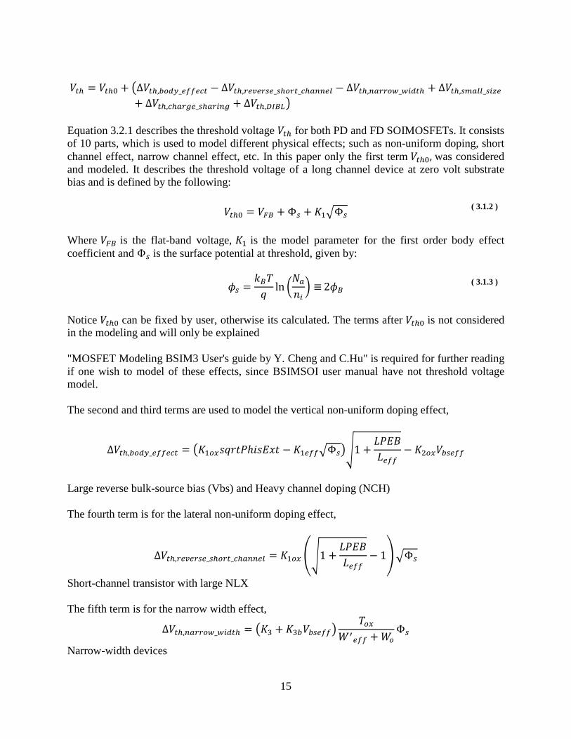
𝑉𝑡ℎ = 𝑉𝑡ℎ0 + �∆𝑉𝑡ℎ,𝑏𝑜𝑑𝑏_𝑑𝑜𝑜𝑑𝑓𝑡 − ∆𝑉𝑡ℎ,𝑟𝑑𝑣𝑑𝑟𝑑𝑑_𝑑ℎ𝑜𝑟𝑡_𝑓ℎ𝑑𝑜𝑜𝑑𝑎 − ∆𝑉𝑡ℎ,𝑜𝑑𝑟𝑟𝑜𝑤_𝑤𝑖𝑑𝑡ℎ + ∆𝑉𝑡ℎ,𝑑𝑚𝑑𝑎𝑎_𝑑𝑖𝑠𝑑
+ ∆𝑉𝑡ℎ,𝑓ℎ𝑑𝑟𝑔𝑑_𝑑ℎ𝑑𝑟𝑖𝑜𝑔 + ∆𝑉𝑡ℎ,𝐷𝐷𝐵𝐵� Equation 3.2.1 describes the threshold voltage 𝑉𝑡ℎ for both PD and FD SOIMOSFETs. It consists of 10 parts, which is used to model different physical effects; such as non-uniform doping, short channel effect, narrow channel effect, etc. In this paper only the first term 𝑉𝑡ℎ0, was considered and modeled. It describes the threshold voltage of a long channel device at zero volt substrate bias and is defined by the following: 𝑉𝑡ℎ0 = 𝑉𝐹𝐵 + Φ𝑑 + 𝐾1�Φ𝑑
( 3.1.2 )
Where 𝑉𝐹𝐵 is the flat-band voltage, 𝐾1 is the model parameter for the first order body effect coefficient and Φ𝑑 is the surface potential at threshold, given by:
𝜙𝑑 =𝑚𝐵𝑚𝑞
ln �𝑁𝑑𝑛𝑖� ≡ 2𝜙𝐵 ( 3.1.3 )
Notice 𝑉𝑡ℎ0 can be fixed by user, otherwise its calculated. The terms after 𝑉𝑡ℎ0 is not considered in the modeling and will only be explained "MOSFET Modeling BSIM3 User's guide by Y. Cheng and C.Hu" is required for further reading if one wish to model of these effects, since BSIMSOI user manual have not threshold voltage model. The second and third terms are used to model the vertical non-uniform doping effect,
∆𝑉𝑡ℎ,𝑏𝑜𝑑𝑏_𝑑𝑜𝑜𝑑𝑓𝑡 = �𝐾1𝑜𝑜𝑠𝑞𝑠𝑡𝑠ℎ𝑖𝑠𝑖𝑥𝑡 − 𝐾1𝑑𝑜𝑜�Φ𝑑��1 +𝐿𝑠𝑖𝐿𝐿𝑑𝑜𝑜
− 𝐾2𝑜𝑜𝑉𝑏𝑑𝑑𝑜𝑜
Large reverse bulk-source bias (Vbs) and Heavy channel doping (NCH) The fourth term is for the lateral non-uniform doping effect,
∆𝑉𝑡ℎ,𝑟𝑑𝑣𝑑𝑟𝑑𝑑_𝑑ℎ𝑜𝑟𝑡_𝑓ℎ𝑑𝑜𝑜𝑑𝑎 = 𝐾1𝑜𝑜 ��1 +𝐿𝑠𝑖𝐿𝐿𝑑𝑜𝑜
− 1��Φ𝑑
Short-channel transistor with large NLX The fifth term is for the narrow width effect,
∆𝑉𝑡ℎ,𝑜𝑑𝑟𝑟𝑜𝑤_𝑤𝑖𝑑𝑡ℎ = �𝐾3 + 𝐾3𝑏𝑉𝑏𝑑𝑑𝑜𝑜�𝑚𝑜𝑜
𝑊′𝑑𝑜𝑜 + 𝑊𝑜
Φ𝑑
Narrow-width devices

16
The sixth term is to small size effect in devices with both small channel length and small width.
∆𝑉𝑡ℎ,𝑑𝑚𝑑𝑎𝑎_𝑑𝑖𝑠𝑑 = 𝐷𝑉𝑚0𝑤 �𝑒𝑥𝑒 �−𝐷𝑉𝑚1𝑤𝑊′
𝑑𝑜𝑜𝐿𝑑𝑜𝑜2𝑙𝑡𝑤
� + 2𝑒𝑥𝑒 �−𝐷𝑉𝑚1𝑤𝑊′
𝑑𝑜𝑜𝐿𝑑𝑜𝑜𝑙𝑡𝑤
�� (V𝑏𝑖 − Φ𝑑)
Narrow-width and short-channel transistors The seventh and eighth terms are related to the short channel effect due to DIBL.
∆𝑉𝑡ℎ,𝑓ℎ𝑑𝑟𝑔𝑑_𝑑ℎ𝑑𝑟𝑖𝑜𝑔 = 𝐷𝑉𝑚0 �𝑒𝑥𝑒 �−𝐷𝑉𝑚1𝐿𝑑𝑜𝑜2𝑙𝑡
� + 2𝑒𝑥𝑒 �−𝐷𝑉𝑚1𝑤𝐿𝑑𝑜𝑜𝑙𝑡
�� (V𝑏𝑖 − Φ𝑑)
short-channel transistors
∆𝑉𝑡ℎ,𝐷𝐷𝐵𝐵 = �𝑒𝑥𝑒 �−𝐷𝑑𝑠𝑏𝐿𝑑𝑜𝑜2𝑙𝑡𝑜
� + 2𝑒𝑥𝑒 �−𝐷𝑑𝑠𝑏𝐿𝑑𝑜𝑜𝑙𝑡𝑜
�� �E𝑡𝑑𝑜 − E𝑡𝑑𝑏V𝑏𝑑𝑑𝑜𝑜�V𝑑𝑑
Short-channel devices under large Vds the last two is introduces to capture the DIBL variation in longer channel.
∆𝑉𝑡ℎ,𝐷𝐷𝐵𝐵 = 𝑛𝑣𝑡 ∙ ln�𝐿𝑑𝑜𝑜
𝐿𝑑𝑜𝑜 + 𝐷𝑉𝑚𝑠0 ∙ (1 + 𝑒−𝐷𝑉𝑚𝐷1∙𝑉𝐷𝐷)� −𝐷𝑉𝑚𝑠2𝐿𝑑𝑜𝑜𝐷𝑉𝑚𝐷3
∙ tanh(𝐷𝑉𝑚𝑠4 ∙ 𝑉𝐷𝐷)

17
3.2 Unified I-V Model
A accurate I-V characteristics is also required for a good compact model. The I-V characteristics are mainly influenced by two key factors, channel charge and mobility. The single drain current equation of BSIMSOI will be introduced after all the sub-models are discussed. 3.2.1 Channel Charge Model
BSIMSOI uses the same channel charge model as BSIM3, the unified expression for the channel charge 𝑄𝑓ℎ from strong inversion and subthreshold regions, the channel change density at source end for both subthreshold and inversion region is defined by: 𝑄𝑓ℎ𝑑0 = 𝐶𝑜𝑜𝑉𝑔𝑑𝑡𝑑𝑜𝑜 ( 3.2.1 )
where 𝑉𝑔𝑑𝑡𝑑𝑜𝑜 is the Effective 𝑉𝑔𝑑 − 𝑉𝑡 function introduced to describe the channel charge characteristics from subthreshold to strong inversion. Effective 𝑉𝑔𝑑𝑡 for all regions (with Polysilicon Depletion Effect) is defined as following:
𝑉𝑔𝑑𝑡𝑑𝑜𝑜 =𝑛𝑣𝑡 ln �1 + exp (𝑚
∗�𝑉𝑔𝑔_𝑒𝑒𝑒−𝑉𝑡ℎ�𝑜𝑣𝑡
)�
𝑚∗ + 𝑛𝐶𝑜𝑜�2ϕs
qεsiNdepexp �−
(1−𝑚∗)�𝑉𝑔𝑔_𝑒𝑒𝑒−𝑉𝑡ℎ�−𝑉𝑜𝑒𝑒𝑜𝑣𝑡
� ( 3.2.2 )
where 𝑚∗ = 0.5 +tan−1(𝑀𝐼𝑁𝑉)
𝜋 𝑀𝐷𝑀𝑉=0������ 𝑚∗ = 0.5
MINV is 𝑉𝑔𝑑𝑡𝑑𝑜𝑜 fitting parameter for moderate inversion, the default value is 0. Equation 3.3.11 without Polysilicon depletion becomes:
𝑉𝑔𝑑𝑡𝑑𝑜𝑜 =2𝑛𝑣𝑡 ln �1 + exp (�𝑉𝑔𝑔−𝑉𝑡ℎ�
2𝑜𝑣𝑡)�
1 + 2𝑛𝐶𝑜𝑜�2ϕs
qεsiNdepexp �− 𝑉𝑔𝑔−𝑉𝑡ℎ−2𝑉𝑜𝑒𝑒
2𝑜𝑣𝑡� ( 3.2.3 )
where 𝑉𝑜𝑜𝑜 is the offset voltage in the subthreshold region for large W and L and was added to describe the threshold voltage difference between strong inversion and subthreshold region. 3.2.2 Mobility Model
Mobility is one of the key parameters in a MOSFET model. It describes the relation between drift velocity of electrons or holes and an applied electric field in the semiconductor materials. 𝑣 = µ𝑬 ( 3.2.4 )
where 𝑣 is the drift velocity, 𝑬 is the electric field and µ is the mobility. This topic has been well studied since the 1970's [20], there are three scattering mechanisms proposed to explain the

18
surface mobility of the model: Phonon, coulomb and surface roughness scattering. The figure 3.1 below illustrate that each mechanism is dominant under different conditions, such as varying temperature. Other conditions are bias and doping concentration.
Figure 3. 1. The three dominant scattering mechanisms affecting the mobility in the inversion layer under different
temperature. [20]
Furthermore, the different process parameters and bias condition also affect the mobility. Such as the gate oxide thickness, doping concentration, threshold voltage etc. In order to simplify the model, an empirical unified formulation based on the concept of an effective field is proposed by [21] to compile all the parameters and biases.
𝑖𝑑𝑜𝑜 =𝑄𝐵 + (𝑄𝑜/2)
𝜀𝑑𝑖 ( 3.2.5 )
The unified equation of mobility is given below:
µeff =µ0
1 + (Eeff/E0)v ( 3.2.6 )
For a continuous I-V model, a continuous mobility model is required. BSIMSOI use a unified mobility expression based on the Vgsteff expression of Eq 3.3.7
𝜇𝑑𝑜𝑜 =𝜇0
1 + �𝑈𝐴 + 𝑈𝐶𝑉𝑏𝑑𝑑𝑜𝑜� �𝑉𝑔𝑔𝑡𝑒𝑒𝑒+2𝑉𝑡ℎ
𝑚𝑜𝑜� + 𝑈𝐵 �
𝑉𝑔𝑔𝑡𝑒𝑒𝑒+2𝑉𝑡ℎ𝑚𝑜𝑜
�2 ( 3.2.7 )
Where 𝜇0 is the zero-field mobility parameter in the universal mobility formulation when temp = tnom, 𝑈𝐴 is model parameter for the first-order mobility degradation, 𝑈𝐵 is model parameter for the second-order mobility degradation and 𝑈𝐶 is model parameter for the body-effect of mobility degradation. The body effect is not considered in this work; therefore 3.2.7 can be rewritten into 3.2.8.

19
𝜇𝑑𝑜𝑜 =𝜇0
1 + 𝑈𝐴 �𝑉𝑔𝑔𝑡𝑒𝑒𝑒+2𝑉𝑡ℎ
𝑚𝑜𝑜� + 𝑈𝐵 �
𝑉𝑔𝑔𝑡𝑒𝑒𝑒+2𝑉𝑡ℎ𝑚𝑜𝑜
�2 ( 3.2.8 )
Equation 3.2.8 will be the mobility equation used in parameter extraction and modeling. 3.2.3 Carrier Drift Velocity
Another important parameter in transistor modeling is the carrier drift velocity. Defined in 3.3.9
𝑣 = �𝜇eff𝑖
1 + (𝑖/𝑖sat), E < Esat
𝑣sat, E > Esat ( 3.2.9 )
𝑖sat corresponds to the critical electrical field at which the carrier velocity becomes saturated.
𝑖sat =2𝑣𝑑𝑑𝑡𝜇𝑑𝑜𝑜
( 3.2.10 )
The saturation velocity, 𝑣sat , is given by 𝑖satis the critical field for saturation velocity. 3.2.4 Bulk Charge Effect
In bulk device, the depletion region thickness will not be uniform along the channel when a non-zero 𝑉𝑑𝑑 is applied. As result threshold voltage varies along the channel; this effect is called bulk charge effect. BSIMSOI uses parameter 𝐴𝑏𝑠𝑎𝑏 to model the bulk charge effect and is defined as the following equation:
𝐴𝑏𝑠𝑎𝑏 = 1 + �𝐾1𝑜𝑜 ∙ �1 + 𝐿𝑠𝑖𝐿 𝐿𝑑𝑜𝑜⁄
2�(𝜙𝑑 + 𝐾𝑒𝑡𝐾𝑠) − 𝑉𝑏𝑔ℎ1+𝐵𝑑𝑡𝑑∙𝑉𝑏𝑔ℎ
�𝐴0𝐿𝑑𝑜𝑜
𝐿𝑑𝑜𝑜 + 2�𝑚𝑑𝑖𝑋𝑑𝑑𝑑�1
− 𝐴𝑔𝑑𝑉𝑔𝑑𝑡𝑑𝑜𝑜 �𝐿𝑑𝑜𝑜
𝐿𝑑𝑜𝑜 + 2�𝑚𝑑𝑖𝑋𝑑𝑑𝑑�2
�+𝐿0
𝑊′𝑑𝑜𝑜 + 𝐿1��
( 3.2.11 )
Because the architecture difference between UTB-SOI and Bulk devices, this effect can neglected/simplified for UTB-SOI MOSFET modeling. Generally, for Bulk devices the 𝐴𝑏𝑠𝑎𝑏 is close to 1 if the channel length is small and grows as the channel length increases. Which means the bulk charge effect is small when the channel length is small and grows with the channel length. For the modeling of UTB-SOI, 𝐴𝑏𝑠𝑎𝑏 is assumed to be 1, so few parameters need to set to corresponding value. The parameters 𝐴0 is Bulk charge effect coefficient for channel length and 𝐿0 is Bulk charge effect coefficient for channel width, both will be set to zero so 𝐴𝑏𝑠𝑎𝑏 is equal with 1.

20
3.2.5 The 𝒏 Parameter for Subthreshold Swing The subthreshold swing is determined by the swing factor or slope factor 𝑛, it can be defined as the following:
SS =dVgs
d log Ids≈ 2.3nvt
( 3.2.12 )
The 𝑛 parameter is the key parameter for the devices subthreshold swing
n = 1 +CdepCox
+CitCox
( 3.2.13 )
in BSIMSOI 𝑛 is defined by
𝑛 = 1 + NFACTOR
εsi / XdepCox
+CitCox
+(CDSC + CDSCDVds + CDSCBVbseff) �exp �−DVT1
Leff2lt� + 2exp �−DVT1
Leff2lt��
Cox
( 3.2.14 )
where Xdep is the width of the channel depletion. Parameter NFACTOR Introduced to cover for any uncertainty in the calculation of the depletion capacitance and is determined experimentally. Citis called the interface depletion capacitance and accounts for the influence of the interface charge density.CDSC, CDSCD, CDSCBare parameters to describe the coupling effects between the drain and the channel due to the DIBL effect.In this thesis, the short channel effect parameters are assumed to be equal zero, Eq 2.1.14 can be written as the following expression:
𝑛 = 1 + NFACTORεsi / Xdep
Cox+
CitCox
+(CDSC)
Cox
( 3.2.15 )
Figure 3. 2. gate oxide capacitance, channel depletion capacitance and coupling capacitances.

21
3.2.6 Unified Drain Equation of BSIMSOI
The drain equations in semiconductor courses are often defined as eq. 2.1.1. In BSIMSOI, one single drain current equation is designed to link all the operating regions [23]:
𝐼𝑑𝑑 =𝐼𝑑𝑑0
1 + 𝑅𝑑𝑔𝐷𝑑𝑔0𝑉𝑑𝑔𝑒𝑒𝑒
�1 +𝑉𝑑𝑑 − 𝑉𝑑𝑑𝑑𝑜𝑜
𝑉𝐴� ( 3.2.16 )
where 𝛽 is given by:
𝛽 = 𝜇𝑑𝑜𝑜𝐶𝑜𝑜𝑊𝑑𝑜𝑜
𝐿𝑑𝑜𝑜 ( 3.2.17 )
𝐼𝑑𝑑0 is defined as:
𝐼𝑑𝑑0 =𝛽𝑉𝑔𝑑𝑡𝑑𝑜𝑜 �1 − 𝐴𝑏𝑠𝑎𝑏
𝑉𝑑𝑔𝑒𝑒𝑒2�𝑉𝑔𝑔𝑡𝑒𝑒𝑒+2𝑉𝑡�
� 𝑉𝑑𝑑𝑑𝑜𝑜
1 + 𝑉𝑑𝑔𝑒𝑒𝑒𝐸𝑔𝑠𝑡𝐵𝑒𝑒𝑒
( 3.2.18 )
and 𝑉𝑑𝑑𝑑𝑜𝑜 is the effective source-drain bias (Eq. 3.3.20), 𝑅𝑑𝑑 is the source/drain series resistance, 𝜇𝑑𝑜𝑜 is the effective mobility calculated in Equation: 3.3.8. 𝑉𝐴 account for channel length modulation (CLM) and drain-induced barrier lowering (DIBL) and is expressed as the following equation:
𝑉𝐴 = 𝑉𝐴𝑑𝑑𝑡 + �1 +𝑠𝑣𝑑𝑔𝑉𝑔𝑑𝑡𝑑𝑜𝑜𝑖𝑑𝑑𝑡𝐿𝑑𝑜𝑜
� �1
𝑉𝐴𝐶𝐵𝑀+
1𝑉𝐴𝐷𝐷𝐵𝐵𝐶
�−1
( 3.2.19 )
where VACLM account the effect of channel length modulation and VADIBLC for drain-induced barrier lowering. 𝑉𝐴𝑑𝑑𝑡 is 𝑉𝐴 at saturation point where (Vds=Vdsat). For intrinsic case (Rds = 0), Vdsat is define by
Vdsat =EsatLeff�Vgsteff + 2Vt�
AbulkEsatLeff + �Vgsteff + 2Vt� ( 3.2.20 )
where 𝑖𝑑𝑑𝑡 is the critical electrical field at which the carrier velocity becomes saturated.
𝑖𝑑𝑑𝑡 =2𝑣𝑑𝑑𝑡𝜇𝑑𝑜𝑜
( 3.2.21 )
Since CLM and DIBL is not modeled and 𝑖𝑑𝑑𝑡 is assumed to be infinite. As a result parameter 𝑉𝐴 will in addition be infinite due to 𝑉𝐴𝑑𝑑𝑡 = ∞. The single drain current equation can be simplified to the following:

22
𝐼𝑑𝑑 ≈ 𝜇𝑑𝑜𝑜𝐶𝑜𝑜𝑊𝑑𝑜𝑜
𝐿𝑑𝑜𝑜𝑉𝑔𝑑𝑡𝑑𝑜𝑜 �1 −
𝑉𝑑𝑑𝑑𝑜𝑜2�𝑉𝑔𝑑𝑡𝑑𝑜𝑜 + 2𝑣𝑡�
�𝑉𝑑𝑑𝑑𝑜𝑜 ( 3.2.22 )
and Vdseff function is introduced to guarantee continuities of Id and its derivatives at Vdsat
Vdseff = Vdsat −12�Vdsat − Vds − δ + �(Vdsat − Vds − δ)2 + 4δVdsat� ( 3.2.23 )
where δ is a user specified parameter with a default value of 0.01.
3.3 Model Selector SOIMOD BSIMSOI is developed with BSIM3 and BSIMPD as foundations, it's a unified model for both PD and FD SOI MOSFET based on the concept of body-source build-in potential lowering [22]. It's a concept that unify both PD and FD SOI modeling, where the difference between the PD and FD is modeled by build-in potential lowering ∆𝑉𝑏𝑖 , as an indication for the degree of depletion. There are four modes in BSIMSOI: BSIMPD (soiMod = 0) is for PD-SOI MOSFETs modeling, unified SOI model (soiMod = 1), ideal FD model (soiMod = 2) is used to model FD device. There is no body node and the body current/charge calculation is skipped. Furthermore, the body voltage Vbs is pinned at ∆Vbi = Vbs0.
∆Vbi = Vbs0 =
CsiCSi + CBOX
∙ �𝜙 −qNch
2εSi∙ Tsi2 + Vnonideal + ∆VDIBL�
+ ηeCBOX
CSi + CBOX(Ves − VFBb)
( 3.3.1 )
where
𝐶𝑑𝑖 =𝜀𝑑𝑖𝑚𝑑𝑖
,𝐶𝐵𝑂𝑂 =𝜀𝑂𝑂𝑚𝐵𝑂𝑂
,𝐶𝑂𝑂 =𝜀𝑂𝑂𝑚𝑂𝑂
Vnonideal is the offset voltage due to non-idealities, ∆𝑉𝐷𝐷𝐵𝐵accounts the short channel effect on ∆𝑉𝑏𝑖 and 𝜂𝑑 for the short channel effect on the backgate coupling. These three values is assumed to be zero when modeling, the new ∆Vbi
∆𝑉𝑏𝑖 = 𝑉𝑏𝑑0 =𝐶𝑑𝑖
𝐶𝐷𝑖 + 𝐶𝐵𝑂𝑂∙ �𝜙 −
𝑞𝑁𝑓ℎ2𝜀𝐷𝑖
�
( 3.3.2 )
where

23
𝜙 = Φ𝑂𝑀 −𝐶𝑂𝑂
𝐶𝑂𝑂 + �𝐶𝐷𝑖−1 + 𝐶𝐵𝑂𝑂−1�−1 ∙ 𝑁𝑂𝐹𝐹,𝐹𝐷𝑣𝑡
∙ ln�1 + 𝑒𝑥𝑒 �𝑉𝑡ℎ,𝐹𝐷 − 𝑉𝑔𝑑_𝑑𝑜𝑜 − 𝑉𝑂𝐹𝐹,𝐹𝐷
𝑁𝑂𝐹𝐹,𝐹𝐷𝑣𝑡��
( 3.3.3 )
𝑁𝑂𝐹𝐹,𝐹𝐷 and 𝑉𝑂𝐹𝐹,𝐹𝐷are model parameters to improve the transition between subthreshold and strong inversion regions, 𝑣𝑡 is the thermal voltage and the surface band bending at strong inversion, Φ𝑂𝑀 is given by:
Φ𝑂𝑀 = 2Φ𝐵
( 3.3.4 )
3.4 Real Device effects Real physical device effects are important for representing the output characteristics of SOI MOSFETs. The real device effects considered in BSIM-SOI are listed in table below [23]; some of them are modeled in this paper, for further reading about these real device effects, references are listed in Appendix B.
Table 2. 1. Real device effect modules in BSIMSOI
Real device effect module 1 Short Channel Effects 2 Vth roll-off 3 Subthreshold Swing Degradation 4 Drain Induced Barrier Lowering 5 Channel Length Modulation 6 Source/Drain Series Resistance 7 Parasitic Capacitance 8 Mobility Degradation 9 Poly Depletion Effect 10 Velocity Saturation 11 Velocity Overshoot 12 Gate Induced Drain Leakage 13 Source/Drain Junction Leakage 14 Impact Ionization 15 Temperature effects and self-heating

24
Chapter 4 Parameter Extraction and Modeling of KTH MOSFET
Parameter extraction is an important part of device modeling. Depending on the model, there is different methodology used for the extraction. In this section, the BSIMSOI suggested extraction method will be reviewed. Furthermore, the parameter extraction result will be presented.
4.1 Overview
There are several extraction and optimization methods when it comes to extraction of model parameters. The commercial extraction software often use global optimization to extract all the model parameters at once, the one set of parameters will fit all the experimental data but the globally optimized parameters often doesn't have any resemblance to its actual physical value. Opposite of global optimization there is local optimization. Local optimization is performed for different operation regions where different device behaviors are dominant. The locally optimized parameters don’t fit well with the experimental data in all device operating regions. However they show close resemblance to the physical value. Furthermore, there are also device geometry related methods for the parameter extraction: Single device extraction and group device extraction. The first method use only one type of device geometry to extract all of the model parameters, the extracted values fit only to the same type of device very well and don’t fit with other device geometries. This method is often used in the early days, when the device geometry had little effect on the device models. It is no longer practical since extraction with only one channel length and width cannot determine parameters with channel length and channel width dependencies, such as short channel effects and narrow width effects. Nowadays, group extraction method is often used in model parameter extraction where experimental data from multiple devices with different length and width are used. The advantage of this method is it can fit many devices with different geometries. BSIMSOI is based on the BSIM3 core models [24]; therefore the extraction routines are almost identical. One start with a combination of local optimization and group device extraction strategy to obtain the preliminary parameters, then a global optimization can be used to improve the overall accuracy between the model and the measurement. In this paper, due to lack of group device measurements, a local optimized and single device extraction is performed to illustrate the basic models in BSIMSOI and modeling of KTH MOSFET. 4.1.1 Optimization method The optimization process used in this paper is a combination of Newton-Raphson iteration and a linear least-square fit routine. The model equation with one, two, or three variables need to be first arranged in a form suitable for the iteration equation 4.2.1 given by [25]:
𝑓𝑑𝑜𝑑(𝑠10,𝑠20,𝑠30) − 𝑓𝑑𝑖𝑚�𝑠1(𝑚),𝑠2
(𝑚),𝑠3(𝑚)�
=𝜕𝑓𝑑𝑖𝑚𝜕𝑠1
∆𝑠1𝑚 +𝜕𝑓𝑑𝑖𝑚𝜕𝑠2
∆𝑠2𝑚 +𝜕𝑓𝑑𝑖𝑚𝜕𝑠3
∆𝑠3𝑚
( 4.1.1 )
where f() is the function to be optimized, parameters 𝑠1,𝑠2 and 𝑠3 are to be extracted,

25
𝑠10,𝑠20and 𝑠30are the true physical values. 𝑠1(𝑚), 𝑠2
(𝑚)and 𝑠3(𝑚) are the parameter values after
the m-th iteration. Figure 4.1 below describe the procedures of the optimization.
Figure 4. 1. Flowchart of the optimization process [25]

26
4.1.2 Process parameters and I-V Measurements The Table 4.1 below is the process parameters for the KTH UTBSOI MOSFET.
Table 4. 1. KTH transistor parameters
Parameter Physical meaning Value Unit 𝑻𝒐𝒐 Thickness of gate oxide 5x10^-9 m 𝑻𝒔𝒔 Thickness of silicon film 2x10^-8 m 𝑻𝒃𝒐𝒐 Thickness of buried oxide 1.45x10^-7 m 𝑵𝒄𝒄 Doping concentration in channel 1x10^+15 1/cm3
𝑵𝒔𝒔𝒃 Doping concentration in substrate 6x10^+16 1/cm3 𝑳 Channel length 1x10^-6 m 𝑾 Channel width 1x10^-5 m 𝑿𝒋 Junction depth 𝑻𝒔𝒔 m
The BSIMSOI manual suggested I-V measurement for basic MOS I-V parameters:
• 𝐼𝑑𝑑 vs. 𝑉𝑔𝑑 @ Small 𝑉𝑑𝑑 and 𝑉𝑑𝑑 = 0V. • 𝐼𝑑𝑑 vs. 𝑉𝑔𝑑 @ 𝑉𝑑𝑑 = 𝑉𝑑𝑑 and 𝑉𝑑𝑑 = 0V. • 𝐼𝑑𝑑 vs. 𝑉𝑑𝑑 @ with different 𝑉𝑔𝑑 and 𝑉𝑑𝑑 = 0V.
Drain was biased to Vds, Gate was biased to Vgs, Source was biased to zero and Substrate is biased to zero. Figure 4.2 illustrate the transistor schematic simulated in cadence. Where G is gate, D is drain, S is source and E is the body bias.
Figure 4. 2. Schematic of Cadence simulation

27
4.2 Extraction of the threshold voltage The extrapolation in linear region method is the most popular threshold-voltage extraction method, it consist of finding the gate-voltage intercept at Id=0 of the extrapolated maximum first derivative slope. The numbers of steps are described below:
1. Measure Ids − Vgs characteristics at low Vds(<0.1V) 2. Determine the maximum slope of Ids − Vgs curve, at the maximum gm point. 3. Extrapolate Ids − Vgs from the maximum gm point to Ids = 0. 4. Find the corresponding extrapolated Vgs value (Vgs0) for Ids = 0. 5. Calculate Vth according to Vth = Vgs0 − 0.5 Vds.
The Matlab script function ExtractVth (see appendix A) follows the extraction steps, extract the threshold voltage value for specific drain current and print out a figure with maximum slope. Figure 4.3 below illustrate the Ids-Vgs curve, transconductance curve and the maximum slope.
Figure 4. 3. linear region drain current Id, transconductance gm vs Vgs and maximum slope curve. Symbols: KTH
measurements, Lines: Matlab fit
The Extracted threshold voltage values are shown below in Table 4.1.
Table 4. 2. Extracted threshold voltages
𝑉𝑡ℎ NMOS 𝑉𝑡ℎ PMOS Extracted value 0.443 V -0.426 V Reference data 0.51±0.023 V -0.49±0.036 V

28
Figure 4. 4. NMOS 308 Batch
The same batch of transistors has the average threshold voltage value as 0.51+/-0.023.
4.3 Extraction of the mobility parameters The fitting target data for the mobility parameters is the strong inversion region. The body effect is assumed to be negligible, thus the body-effect of mobility degradation coefficient Uc is equal zero. The new effective mobility equation shows below:
𝜇𝑑𝑜𝑜 =𝜇0
1 + 𝑈𝐴 �𝑉𝑔𝑔𝑡𝑒𝑒𝑒+2𝑉𝑡ℎ
𝑚𝑜𝑜� + 𝑈𝐵 �
𝑉𝑔𝑔𝑡𝑒𝑒𝑒+2𝑉𝑡ℎ𝑚𝑜𝑜
�2
Equation 2.5.10 can rewrite as the following relations:
𝜇𝑑𝑜𝑜𝑉𝑔𝑑𝑡𝑑𝑜𝑜 + 2𝑉𝑡ℎ
𝑚𝑜𝑜= 𝐴, �
𝑉𝑔𝑑𝑡𝑑𝑜𝑜 + 2𝑉𝑡ℎ𝑚𝑜𝑜
�2
= 𝐴2 = 𝐿 ( 4.3.1 )
𝜇𝑑𝑜𝑜 =
𝜇01 + 𝑈𝐴𝐴+𝑈𝐵𝐿
( 4.3.2 )
𝜇𝑑𝑜𝑜 = 𝜇0 − 𝜇𝑑𝑜𝑜𝑈𝐴𝐴 − 𝜇𝑑𝑜𝑜𝑈𝐵𝐿 ( 4.3.3 )
Rewrite the equations 4.3.3 to fit inside the optimizing equation 4.1.1:
𝑓𝑑𝑖𝑚 = 𝜇0 − 𝜇𝑑𝑜𝑜𝑈𝐴𝐴 − 𝜇𝑑𝑜𝑜𝑈𝐵𝐿 − 𝜇𝑑𝑜𝑜 = 0
𝜕𝑓𝑑𝑖𝑚𝜕𝜇0
= 1,𝜕𝑓𝑑𝑖𝑚𝜕𝑈𝐴
= −𝜇𝑑𝑜𝑜𝐴,𝜕𝑓𝑑𝑖𝑚𝜕𝑈𝐵
= −𝜇𝑑𝑜𝑜𝐿
𝑓𝑑𝑜𝑑(𝜇00,𝑈𝐴0,𝑈𝐵0) − 𝑓𝑑𝑖𝑚�𝜇0(𝑚),𝑈𝐴(𝑚),𝑈𝐵
(𝑚)�= ∆𝜇0𝑚 + −𝜇𝑑𝑜𝑜𝐴∆𝑈𝐴𝑚 − 𝜇𝑑𝑜𝑜𝐿∆𝑈𝐵𝑚
( 4.3.4 )
29
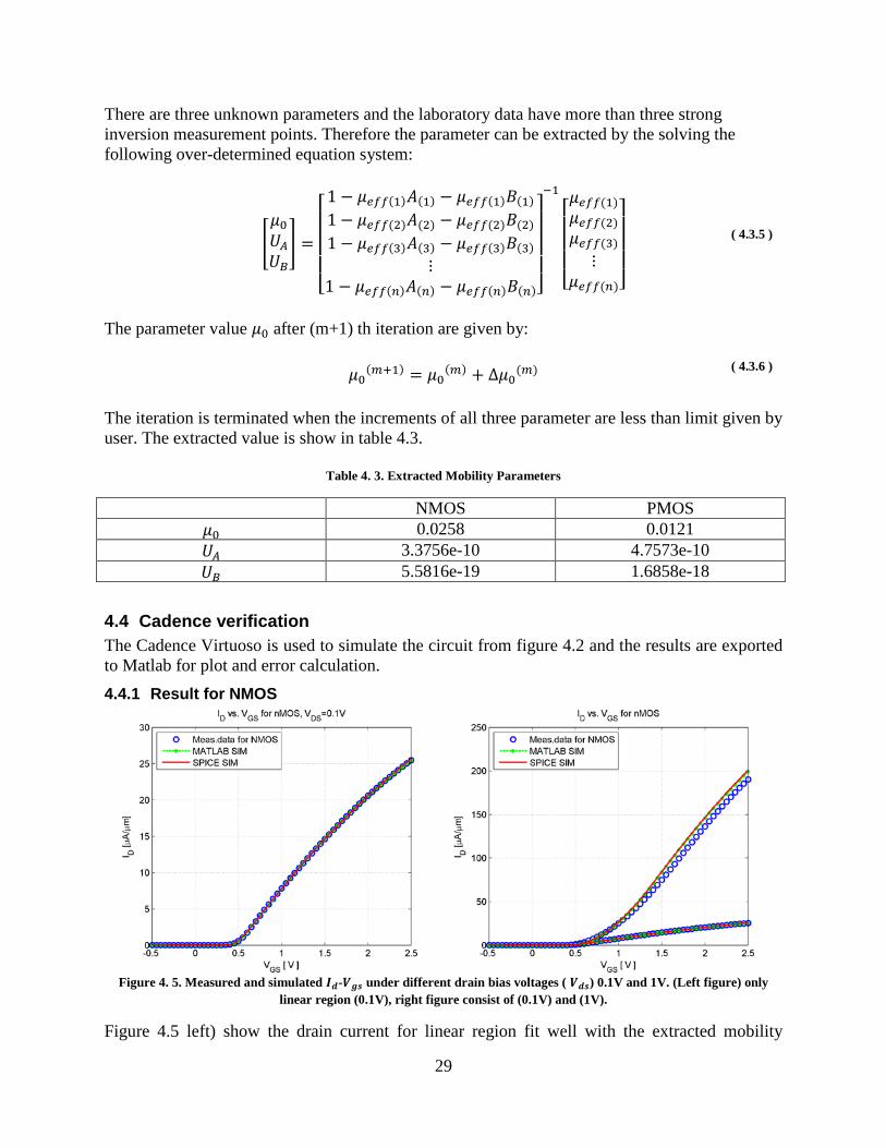
There are three unknown parameters and the laboratory data have more than three strong inversion measurement points. Therefore the parameter can be extracted by the solving the following over-determined equation system:
�𝜇0𝑈𝐴𝑈𝐵� =
⎣⎢⎢⎢⎢⎡
1 − 𝜇𝑑𝑜𝑜(1)𝐴(1) − 𝜇𝑑𝑜𝑜(1)𝐿(1)1 − 𝜇𝑑𝑜𝑜(2)𝐴(2) − 𝜇𝑑𝑜𝑜(2)𝐿(2)1 − 𝜇𝑑𝑜𝑜(3)𝐴(3) − 𝜇𝑑𝑜𝑜(3)𝐿(3)
⋮1 − 𝜇𝑑𝑜𝑜(𝑜)𝐴(𝑜) − 𝜇𝑑𝑜𝑜(𝑜)𝐿(𝑜)⎦
⎥⎥⎥⎥⎤−1
⎣⎢⎢⎢⎡𝜇𝑑𝑜𝑜(1)𝜇𝑑𝑜𝑜(2)𝜇𝑑𝑜𝑜(3)
⋮𝜇𝑑𝑜𝑜(𝑜)⎦
⎥⎥⎥⎤
( 4.3.5 )
The parameter value 𝜇0 after (m+1) th iteration are given by: 𝜇0(𝑚+1) = 𝜇0(𝑚) + ∆𝜇0(𝑚) ( 4.3.6 )
The iteration is terminated when the increments of all three parameter are less than limit given by user. The extracted value is show in table 4.3.
Table 4. 3. Extracted Mobility Parameters
NMOS PMOS 𝜇0 0.0258 0.0121 𝑈𝐴 3.3756e-10 4.7573e-10 𝑈𝐵 5.5816e-19 1.6858e-18
4.4 Cadence verification The Cadence Virtuoso is used to simulate the circuit from figure 4.2 and the results are exported to Matlab for plot and error calculation. 4.4.1 Result for NMOS
Figure 4. 5. Measured and simulated 𝑰𝒅-𝑽𝒈𝒔 under different drain bias voltages ( 𝑽𝒅𝒔) 0.1V and 1V. (Left figure) only
linear region (0.1V), right figure consist of (0.1V) and (1V).
Figure 4.5 left) show the drain current for linear region fit well with the extracted mobility
30
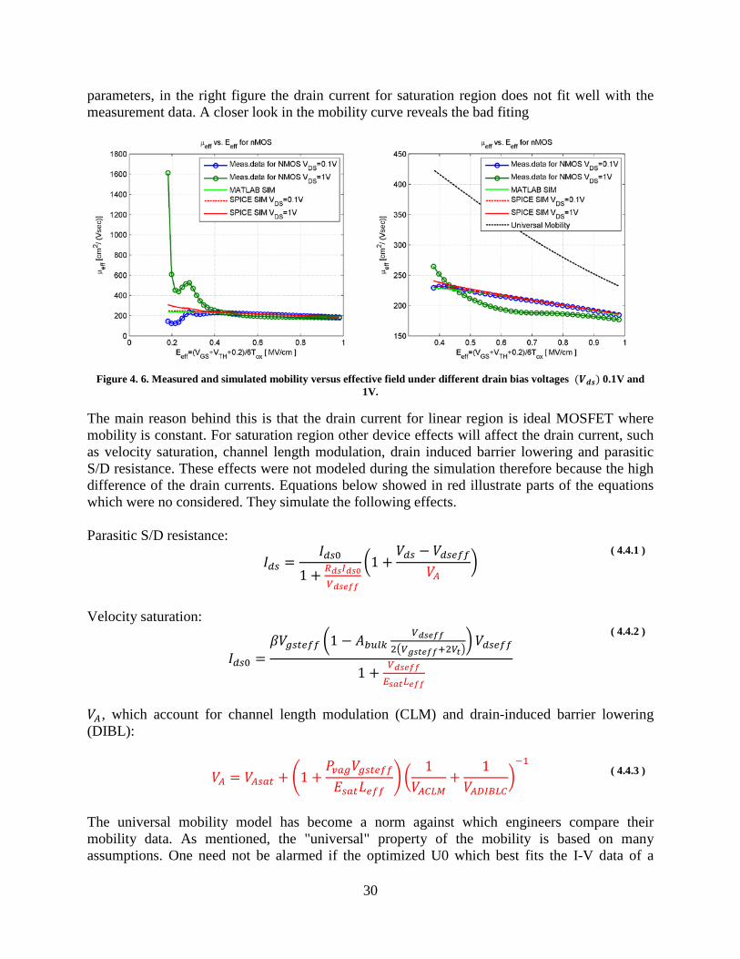
parameters, in the right figure the drain current for saturation region does not fit well with the measurement data. A closer look in the mobility curve reveals the bad fiting
Figure 4. 6. Measured and simulated mobility versus effective field under different drain bias voltages (𝑽𝒅𝒔) 0.1V and 1V.
The main reason behind this is that the drain current for linear region is ideal MOSFET where mobility is constant. For saturation region other device effects will affect the drain current, such as velocity saturation, channel length modulation, drain induced barrier lowering and parasitic S/D resistance. These effects were not modeled during the simulation therefore because the high difference of the drain currents. Equations below showed in red illustrate parts of the equations which were no considered. They simulate the following effects. Parasitic S/D resistance:
𝐼𝑑𝑑 =𝐼𝑑𝑑0
1 + 𝑅𝑑𝑔𝐷𝑑𝑔0𝑉𝑑𝑔𝑒𝑒𝑒
�1 +𝑉𝑑𝑑 − 𝑉𝑑𝑑𝑑𝑜𝑜
𝑉𝐴�
( 4.4.1 )
Velocity saturation:
𝐼𝑑𝑑0 =𝛽𝑉𝑔𝑑𝑡𝑑𝑜𝑜 �1 − 𝐴𝑏𝑠𝑎𝑏
𝑉𝑑𝑔𝑒𝑒𝑒2�𝑉𝑔𝑔𝑡𝑒𝑒𝑒+2𝑉𝑡�
� 𝑉𝑑𝑑𝑑𝑜𝑜
1 + 𝑉𝑑𝑔𝑒𝑒𝑒𝐸𝑔𝑠𝑡𝐵𝑒𝑒𝑒
( 4.4.2 )
𝑉𝐴 , which account for channel length modulation (CLM) and drain-induced barrier lowering (DIBL):
𝑉𝐴 = 𝑉𝐴𝑑𝑑𝑡 + �1 +𝑠𝑣𝑑𝑔𝑉𝑔𝑑𝑡𝑑𝑜𝑜𝑖𝑑𝑑𝑡𝐿𝑑𝑜𝑜
� �1
𝑉𝐴𝐶𝐵𝑀+
1𝑉𝐴𝐷𝐷𝐵𝐵𝐶
�−1
( 4.4.3 )
The universal mobility model has become a norm against which engineers compare their mobility data. As mentioned, the "universal" property of the mobility is based on many assumptions. One need not be alarmed if the optimized U0 which best fits the I-V data of a

31
device is not close to 670 cm2/V-s (for NMOS). It is not uncommon to see values between 350 and 700 cm2/V-s. In fact, the U0 in a sample NMOS model card provided in the official BSIM3 website has a value of 388cm2/V-s. For the subthreshold region, the initial fitting is illustrate by figure 4.7 left), its shifted due to threshold voltage or short channel effects. The theoretical threshold voltages 𝑉𝑡ℎ,𝑑𝑠𝑏 for subthreshold current is different from the threshold voltage that is used to fit strong inversion I-V characteristics. Therefore BSIMSOI account this with Voff parameter, and the threshold voltage for subthreshold current is given by: 𝑉𝑡ℎ,𝑑𝑠𝑏 = 𝑉𝑡ℎ + 𝑉𝑜𝑜𝑜 ( 4.4.4 )
𝑉𝑜𝑜𝑜 is determined experimentally from measured I-V characteristics and is expected to be negative. the recommended range for 𝑉𝑜𝑜𝑜 is between -0.06 and -0.12 V. For the KTH MOSFET the Voff is determined around -0.22 V. Figure 4.7 right) show the logarithmic plot of Ids versus Vgs with the consideration of Voff.
Figure 4. 7. Drain current versus gate voltage at 0.1V and 1V drain voltage. (Symbols: Measurements; Dot Lines: Matlab
simulation; Lines: Model simulated with Cadence)
Figure 4. 8: Drain current versus drain voltage for different front-gate bias.

32
4.4.2 Result for PMOS The results of PMOS are illustrated below in Matlab simulation.
Figure 4. 9. Measured and simulated 𝑰𝒅-𝑽𝒈𝒔 under different drain bias voltages ( 𝑽𝒅𝒔) -0.1V and -1V. (Left figure) normal
plot (Right figure) logarithmic plot
Figure 4. 10. Mobility versus gate voltage for -0.1V and -1V drain bias

33
4.4.3 Error analysis The error between measurement data and simulation is calculated with the RMS Error equation below Mean absolute error and root mean square error:
𝑅.𝐴 𝑖𝑠𝑠𝐸𝑠 =1𝑛��𝑦𝑑𝑖𝑚_𝑖 − 𝑦𝑚𝑑𝑑𝑑_𝑖�
2𝑜
𝑖=1
( 4.4.5 )
𝑅.𝑀. 𝑆 𝑖𝑠𝑠𝐸𝑠 = �1𝑛��𝑦𝑑𝑖𝑚_𝑖 − 𝑦𝑚𝑑𝑑𝑑_𝑖�
2𝑜
𝑖=1
( 4.4.6 )
Table 4. 4. Error analysis of the simulated drain current
NMOS Matlab simulation data Cadence simulation data Drain Current MA Error RMS Error MAE Error RMS Error
Linear Vds=0.1V 0.022 0.035 0.027 0.049 Saturation Vds=1V 4.050 5.855 4.469 6.468
The error in linear region and small 𝑉𝑔𝑑 value of saturation is in good levels the square root of the mean/average of the square of all of the error. Another way to verify the simulation is to take the first derivate of ids vs Vgs curve, which gives the transconductance. Figure 4.11 compare the transconductance between the simulations and laboratory measurements.
Figure 4. 11. NMOS transconductance versus gate voltage at 0.1V and 1.0V drain voltage.
Table 4. 5. Error analysis of the simulated Transconductance
NMOS Matlab simulation data Cadence simulation data Transconductance MA Error RMS Error MAE Error RMS Error Linear Vds=0.1V 0.206 0.329 0.227 0.350
Saturation Vds=1V 4.374 7.153 4.457 7.389 The higher error in Cadence is expected due to other default parameters are considered and
cannot simply shut off in BSIMSOI.

34
Chapter 5 Conclusion and Future work
In this section, the work of this paper is summarized and future work directions are suggested.
5.1 Conclusion
The semiconductor industry has made great progress since the creation of solid state transistor in 1947; great innovations are needed to ensure the continuity of Moore's law. As the transistor scaling becomes more difficult new technology arises, thin-body transistor structures such as FDSOI MOSFET and FinFET. Compact modeling is the bridge between the world of design and manufacturing, compact modeling of FDSOI and multi-gate FET is essential for future device fabrication. This thesis focused on the modeling of KTH FDSOI transistor, with help of BSIMSOI compact model, a basic simulation result of I-V characteristic have been obtained. Nevertheless, the simulation fit only with some portion of KTH measurement. Therefore, more model parameters are needed to ensure the perfect fitting of the transistor.
5.2 Future work
UTBSOI MOSFET is an excellent candidate for advanced technology nodes, where superior control of short-channel effects. Furthermore there is a possibility where back-gate bias is introduced into UTBSOI, where double-gate is formed. This thesis work covered the basic I-V characteristic of BSIMSOI compact model. The future work includes:
• Extraction of more models parameters
• C-V characteristics. Although this work only discusses the BSIMSOI compact model for UTB MOSFETs, there is newer models such as BSIM-IMG. It's a production ready UTBSOI Model under standardization at Compact Model Council which may be more suitable for future modeling of UTBSOI.

35
References
[1] “1947 – Invention of the Point-Contact Transistor” [Online]. Available: http://www.computerhistory.org/semiconductor/timeline/1947-invention.html. Accessed 2014.
[2] C. Hu, “Modern Semiconductor Devices for Integrated Circuits”. Pearson/Prentice Hall, Chapter 3, 2010.
[3] G. E. Moore, “Cramming more components onto integrated circuits”. Electronics,vol. 38, pp. 114 - 117,
1965.
[4] (Figure 1.1.) Moore’s law [Online] Available: http://betanews.com/2013/10/15/breaking-moores-law/. Accessed 2014.
[5] D. J. Frank, R. H. Dennard, E. Nowak, P. M. Solomon, Y. Taur, and H.S. Wong,“Device Scaling
Limits of Si MOSFETs and Their Application Dependencies”. IEEE, vol. 89, March 2001, pp. 259 - 288.
[6] (Figure 1.2. ) K.J Kuhn, “22nm Device Architecture and Performance Elements”[Online] Available: http://download.intel.com/pressroom/pdf/kkuhn/Kuhn_22nm_Device.pdf Accessed 2014.
[7] B. Ho, “Evolutionary MOSFET Structure and Channel Design for Nanoscale CMOS Technology”. PhD
Thesis. Department of EECS, UC Berkeley.
[8] T. Sakurai, A. Matsuzawa and T. Douseki, “Fully-depleted SOI CMOS Circuits and Technology for Ultralow-power Applications”, Springer-Verlag, 2006
[9] (Figure 1.3. ) Soitec wafer [Online] Available: http://c767204.r4.cf2.rackcdn.com/2a79e34b-bc22-4781-9fcf-86a8b88a51a3.jpg Accessed 2014.
[10] J-P. Colinge, “Silicon-on-Insulator Technology: Materials to VLSI”, Kluwer Academic Pub, 1997.
[11] (Figure 1.6.) Bohr. M and Mistry. K. “Intel’s Revolutionary 22nm Transistor Technology” [Online] Available: http://download.intel.com/newsroom/kits/22nm/pdfs/22nm-details_presentation.pdf Accessed 2014
[12] (Figure 1.5.) N. Paydavosi, S. Venugopalan, Y.S. Chauhan, J.P. Duarte, S. Jandhyala, A.M. Niknejad, C.C Hu, “BSIM - SPICE Models Enabl FinFET and UTB IC Designs”, IEEE Access, 2013
[13] (Table 1.1.) “International Technology Roadmap of Semiconductors (ITRS)”, Austin, TX:SEMATECH, 2013. [Online]. Availabe: www.itrs.net. Accessed 2014.
[14] (Figure 1.7.) S. Venugopalan, “From Poisson to Silicon - Advancing Compact SPICE Models for IC Design”. PhD Thesis.Department of EECS,UC Berkeley. 2013.
[15] “KTH Integrated Devices & Circuits Annuel Report 2009” [Online] Available: http://media.ict.kth.se/ab_2009/ekt.pdf. Accessed 2014.
[16] V. Gudmundsson, P.-E. Hellström, J. Luo, J. Lu, S-L. Zhang, and M. Östling, “Fully Depleted UTB and Trigate N-Channel MOSFETs Featuring Low Temperature PtSi Schottky-Barrier Contacts With Dopant Segregation”.IEEE Electron Device Letters, vol. 30, May. 2009

36
[17] (Figure 2.6.) V. Gudmundsson, “Fabrication, characterization, and modeling of metallic source/drain MOSFET”. PhD Thesis. Department of Integrated Devices and Circuits. KTH Royal Institute of Technology. 2011
[18] Compact Model Coalition http://www.si2.org/?page=1650
[19] Y. Cheng and C. Hu, “MOSFET Modeling & BSIM3 User's Guide". Kluwer Academic Pub, 1999
[20] (Figure 3.1.) S. Takagi, “Onthe Universality of Inversion Layer Mobility in Si MOSFET's”. [Online] Available:http://inst.cs.berkeley.edu/~ee230/sp08/takagi%20universal%20mobility%20I%201994.pdf Accessed 2014
[21] A.G. Sabnis and J.T. Clemens, “Characterization of Electron Velocity in the Inversion (100) Si Surface”. Tech. Digital Int. Electron Devices Meet. 18-21. 1979
[22] P. Su et al., “On the body-source built-in potential lowering of SOI MOSFETs”. IEEE Electron Device Letters, February 2003
[23] UC Berkeley BSIM Group. “BSIMSOIv4.5.0 MOSFET Model Users' Manual”. [Online] Available: http://www-device.eecs.berkeley.edu/bsim/?page=BSIMSOI Accessed 2014
[24] UC Berkeley BSIM Group. “BSIM3v3.3 MOSFET Model Users' Manual”. [Online] Available: http://www-device.eecs.berkeley.edu/bsim/?page=BSIM3_Arc Accessed 2014
[25] M.C. Jeng, “Design and Modeling of Deep-Submicrometer MOSFETs”, PhD thesis, University of California. 1990

37
Appendix A Matlab Code This appendix contains the code written in MATLAB, which was used for parameter extraction.
A.1 ExtractVth This script of function is used to extract the threshold voltage for given type of mosfet, ids, vgs, and vds. function [ Vth ] = ExtractVth( Type,Ids,Vgs,Vds ) clf width = 5; % Width in inches height = 4; % Height in inches alw = 0.75; % AxesLineWidth fsz = 15; % Fontsize lw = 1.5; % LineWidth msz = 6; % MarkerSize if Type == 1; Gm=diff(Ids); [num idx] = max(Gm(:)); i = ind2sub(size(Gm),idx+1); figure [hAx,hLine1,hLine2] = plotyy(Vgs,Ids,Vgs(2:61),abs(Gm)); set(hLine1,'LineStyle','O','LineWidth',lw,'MarkerSize',msz) set(hLine2,'LineStyle','O','LineWidth',lw,'MarkerSize',msz) hold on Slope = fit( Vgs(i-1:1:i+1), Ids(i-1:1:i+1), 'poly1'); hold on c=coeffvalues(Slope); plot(Slope); grid on VGs0=(-c(2)/c(1)); Vth=VGs0-0.5*Vds; xlabel('V_{GS} [ V ]'); ylabel('I_D [ \muA/\mum ]'); y2label= get(hAx(2),'ylabel'); % name the second axis y-label set(y2label,'String','g_m [ \muS/\mum ]')% the important part is 'String' to recognize the text that follows title('I_D vs. V_{GS} for nMOS'); % Move the legend to the top left corner. h = legend( 'I_{ds} vs V_{gs}','Slope','g_{m} vs V_{gs}','Location',

38
'NorthWest' ); % Here we preserve the size of the image when we save it. set(gcf,'InvertHardcopy','on'); set(gcf,'PaperUnits', 'inches'); papersize = get(gcf, 'PaperSize'); left = (papersize(1)- width)/2; bottom = (papersize(2)- height)/2; myfiguresize = [left, bottom, width, height]; set(gcf,'PaperPosition', myfiguresize); % Save the file as PNG print('NMOSVth','-dpng','-r300'); else Gm=diff(Ids); [num idx] = max(Gm(:)); i = ind2sub(size(Gm),idx+1); figure [hAx,hLine1,hLine2] = plotyy(Vgs,Ids,Vgs(2:61),abs(Gm)); set(hLine1,'LineStyle','O','LineWidth',lw,'MarkerSize',msz) set(hLine2,'LineStyle','O','LineWidth',lw,'MarkerSize',msz) hold on Slope = fit( Vgs(i-1:1:i+1), Ids(i-1:1:i+1), 'poly1'); hold on c=coeffvalues(Slope); plot(Slope); grid on VGs0=(-c(2)/c(1)); Vth=VGs0-0.5*Vds; xlabel('V_{GS} [ V ]'); ylabel('I_D [ \muA/\mum ]'); y2label= get(hAx(2),'ylabel'); % name the second axis y-label set(y2label,'String','g_m [ \muS/\mum ]')% the important part is 'String' to recognize the text that follows title('I_D vs. V_{GS} for pMOS'); % Move the legend to the top left corner. h = legend( 'I_{ds} vs V_{gs}','Slope','g_{m} vs V_{gs}','Location', 'NorthEast' ); % Here we preserve the size of the image when we save it. set(gcf,'InvertHardcopy','on'); set(gcf,'PaperUnits', 'inches'); papersize = get(gcf, 'PaperSize'); left = (papersize(1)- width)/2; bottom = (papersize(2)- height)/2;

39
myfiguresize = [left, bottom, width, height]; set(gcf,'PaperPosition', myfiguresize); % Save the file as PNG print('PMOSVth','-dpng','-r300'); return end
A.2 NMOS This script fits the I-V measurement to the BSIMSOI model equations and extract the mobility parameters. clear all, load Data.mat,load measurement.mat, format long % Vgs for NMOS: -0.5V to 2.5V % Ids for NMOS @ Vds=0.1V global NMOS_Idlin global NMOS_Idsat Vth=ExtractVth(1,NMOS_Idlin,VGn,0.1); for i=25 i2=(61-i)+1; for n1=10 for n2=20 for n3=30 Voff=-0.24; Vds=0.1; Idlin=NMOS_Idlin(i:61)*1e-6; VGs=VGn(i:61); % Constants % Tox = 5e-9; % Oxide Thickness [M] T = 300; % Temperture [K] q = 1.602176565e-19; % [C] kB = 1.3806488e-23; % Boltzmanns Constant [eV/K] vt = (kB*T)/q; % Thermal Voltage [mV] epsilon0 = 8.854e-12; % [F/m] epsilonox = 3.9 * epsilon0; % [F/m] epsilonsi = 11.68 * epsilon0; % [F/m] Cox = epsilonox/Tox; W=1e-6; %[m] L=1e-6; %[m] delta = 0.01; % ni=1e16; %[cm^-3] Nch=1e21; %[cm^-3] phis=2*vt*log(Nch/ni); sqrtphi = sqrt(phis)

40
Xdep=sqrt((2*epsilonsi)/(q*Nch))*sqrtphi; Cdep=epsilonsi/Xdep; Nfactor=1; Cdsc=0; Cit=0; n=1+Nfactor*(Cdep/Cox)+(3*Cdsc)/Cox+Cit/Cox; Esat=8e99; Abulk=1; % effective Vgs Vgsteff= (2.*n.*vt.*log(1+exp((VGs-Vth)/(2.*n.*vt))))./(1+2.*n.*Cox.*sqrt((2*phis)./(q.*epsilonsi.*Nch)).*exp(-(VGs-Vth-2*Voff)./(2.*n.*vt))); % saturation current Vdsat = (Esat*L*(Vgsteff + 2*vt))./(Abulk*Esat*L+(Vgsteff + 2*vt)); % Vdseff = Vdsat-0.5.*(Vdsat-Vds-delta+sqrt((Vdsat-Vds-delta).^2+4*delta*Vdsat)); % mobility ueff = Idlin./(Cox *(W/L) .* Vgsteff .* (1-(Vdseff./(2.*Vdsat))).* Vdseff); % linear least square n1= n1; n2= n2; n3= n3; u1 = ((Vgsteff(n1) + 2*Vth)/Tox); u2 = ((Vgsteff(n2) + 2*Vth)/Tox); u3 = ((Vgsteff(n3) + 2*Vth)/Tox); a=ueff(n1); b=ueff(n2); c=ueff(n3); A=[1 -a*u1 -a*u1^2; 1 -b*u2 -b*u2^2; 1 -c*u3 -c*u3^2]; B=[ueff(n1);ueff(n2);ueff(n3)]; C=mldivide(A,B); u0=C(1); ua=C(2); ub=C(3); %x=[u0 ua ub]'; i2=(61-i)+1; % u0=0.067; ua=1e-9; ub=1e-19; x=[u0 ua ub]' % Newton Raphson iteration + for iter=1:5 % 5 iteration steps A=((Vgsteff+2*Vth)./Tox); f=u0-ueff-(ueff.*ua.*A)-(ueff.*ub.*A.^2);

41
disp(norm(f)); % check that the norm(f) degrad to a minimum J=[ones(i2,1) -ueff.*A -ueff.*A.^2]; dx=-J\f; x=x+dx; u0=x(1); ua=x(2); ub=x(3); end Vth x, iter % calculate the Id Vgsteff= (2.*n.*vt.*log(1+exp((VGn-Vth)/(2.*n.*vt))))./(1+2.*n.*Cox.*sqrt((2*phis)./(q.*epsilonsi.*Nch)).*exp(-(VGn-Vth-2*Voff)./(2.*n.*vt))); Vdsat = Vgsteff + 2*vt; Vdseff = Vdsat-0.5.*(Vdsat-Vds-delta+sqrt((Vdsat-Vds-delta).^2+4*delta*Vdsat)); ueff1=u0./(1+ua.*((Vgsteff+2*Vth)./Tox)+ub.*(((Vgsteff+2*Vth)./Tox).^2)); Id1 = ueff1.*(Cox *(W/L) .* Vgsteff.* (1-(Vdseff./(2.*Vdsat))).* Vdseff)./1e-6; Vds1=1; Vdseff = Vdsat-0.5.*(Vdsat-Vds1-delta+sqrt((Vdsat-Vds1-delta).^2+4*delta*Vdsat)); Id2 = ueff1.*(Cox *(W/L) .* Vgsteff.* (1-(Vdseff./(2.*Vdsat))).* Vdseff)./1e-6; % calculate errors difflin=NMOS_Idlin-(Id1); diffsimlin=NMOS_Idlin-(lin35./1e-6); diffsat=NMOS_Idsat-(Id2); diffsimsat=NMOS_Idsat-(sat35./1e-6); MAElin=mean(abs(difflin)) MAEsimlin=mean(abs(diffsimlin)) MAEsat=mean(abs(diffsat)) MAEsimsat=mean(abs(diffsimsat)) rmslin=sqrt(mean((difflin).^2)) rmssimlin=sqrt(mean((diffsimlin).^2)) rmssat=sqrt(mean((diffsat).^2)) rmssimsat=sqrt(mean((diffsimsat).^2)) output=[u01' ua1' ub1']; u01(n1)=x(1); ua1(n1)=x(2); ub1(n1)=x(3);

42
PrintPNG(1,VGn,lin35./1e-6,sat35./1e-6,Id1,Id2) end end end end
A.3 PrintPNG this script of function is used to plot and export PNG file of the figures used in this paper. function [ Y ] = PrintPNG(Type,VGn,Idlin,Idsat,Matlin,Matsat) %UNTITLED3 Summary of this function goes here % Detailed explanation goes here global NMOS_Idlin global NMOS_Idsat global PMOS_Idlin global PMOS_Idsat width = 5; % Width in inches height = 4; % Height in inches alw = 0.75; % AxesLineWidth fsz = 11; % Fontsize lw = 1.5; % LineWidth msz = 6; % MarkerSize % PMOS or NMOS, 1 = NMOS else is PMOS if Type == 1; % Semiplot clf measlin=semilogy(VGn,NMOS_Idlin,'bo','LineWidth',lw,'MarkerSize',msz); hold on; semilogy(VGn,NMOS_Idsat,'bo','LineWidth',lw,'MarkerSize',msz); hold on; matsim=semilogy(VGn,Matlin,'g--*','LineWidth',lw,'MarkerSize',4); hold on; semilogy(VGn,Matsat,'g--*','LineWidth',lw,'MarkerSize',4); hold on; spicesim=semilogy(VGn,Idlin,'r-','LineWidth',lw,'MarkerSize',msz); hold on; semilogy(VGn,Idsat,'r-','LineWidth',lw,'MarkerSize',msz); hold on; grid; xlabel('V_{GS} [ V ]'); ylabel('log(I_D) [\muA/\mum]'); title('log(I_D) vs. V_{GS} for nMOS'); legend([measlin,matsim,spicesim],'Meas.data for NMOS','MATLAB SIM','SPICE SIM',4,'Location','SouthEast'); % Here we preserve the size of the image when we save it. set(gcf,'InvertHardcopy','on');

43
set(gcf,'PaperUnits', 'inches'); papersize = get(gcf, 'PaperSize'); left = (papersize(1)- width)/2; bottom = (papersize(2)- height)/2; myfiguresize = [left, bottom, width, height]; set(gcf,'PaperPosition', myfiguresize); % Save the file as PNG print('NMOSsemiplot','-dpng','-r300'); % Normal Plot clf measlin=plot(VGn,NMOS_Idlin,'bo','LineWidth',lw,'MarkerSize',msz); hold on; plot(VGn,NMOS_Idsat,'bo','LineWidth',lw,'MarkerSize',msz); hold on; matsim=plot(VGn,Matlin,'g--*','LineWidth',lw,'MarkerSize',4); hold on; plot(VGn,Matsat,'g--*','LineWidth',lw,'MarkerSize',4); hold on; spicesim=plot(VGn,Idlin,'r-','LineWidth',lw,'MarkerSize',msz); hold on; plot(VGn,Idsat,'r-','LineWidth',lw,'MarkerSize',msz); hold on; grid; xlabel('V_{GS} [ V ]'); ylabel('I_D [\muA/\mum]'); title('I_D vs. V_{GS} for nMOS'); legend([measlin,matsim,spicesim],'Meas.data for NMOS','MATLAB SIM','SPICE SIM',4,'Location','NorthWest'); % Here we preserve the size of the image when we save it. set(gcf,'InvertHardcopy','on'); set(gcf,'PaperUnits', 'inches'); papersize = get(gcf, 'PaperSize'); left = (papersize(1)- width)/2; bottom = (papersize(2)- height)/2; myfiguresize = [left, bottom, width, height]; set(gcf,'PaperPosition', myfiguresize); % Save the file as PNG print('NMOSplot','-dpng','-r300'); % linear ids plot clf measlin=plot(VGn,NMOS_Idlin,'bo','LineWidth',lw,'MarkerSize',msz); hold on; matsim=plot(VGn,Matlin,'g--*','LineWidth',lw,'MarkerSize',4); hold on; spicesim=plot(VGn,Idlin,'r-','LineWidth',lw,'MarkerSize',msz); hold on; grid; xlabel('V_{GS} [ V ]'); ylabel('I_D [\muA/\mum]'); title('I_D vs. V_{GS} for nMOS, V_{DS}=0.1V'); legend([measlin,matsim,spicesim],'Meas.data for NMOS','MATLAB SIM','SPICE SIM',4,'Location','NorthWest');
44
% Here we preserve the size of the image when we save it. set(gcf,'InvertHardcopy','on'); set(gcf,'PaperUnits', 'inches'); papersize = get(gcf, 'PaperSize'); left = (papersize(1)- width)/2; bottom = (papersize(2)- height)/2; myfiguresize = [left, bottom, width, height]; set(gcf,'PaperPosition', myfiguresize); % Save the file as PNG print('NMOSlin','-dpng','-r300'); % plot of gm clf measlin=plot(VGn(1:60),diff(NMOS_Idlin),'bo','LineWidth',lw,'MarkerSize',msz); hold on; plot(VGn(1:60),diff(NMOS_Idsat),'bo','LineWidth',lw,'MarkerSize',msz); hold on; matsim=plot(VGn(1:60),diff(Matlin),'g--*','LineWidth',lw,'MarkerSize',4); hold on; plot(VGn(1:60),diff(Matsat),'g--*','LineWidth',lw,'MarkerSize',4); hold on; spicesim=plot(VGn(1:60),diff(Idlin),'r-','LineWidth',lw,'MarkerSize',msz); hold on; plot(VGn(1:60),diff(Idsat),'r-','LineWidth',lw,'MarkerSize',msz); hold on; grid; xlabel('V_{GS} [ V ]'); ylabel('I_D [\muS/\mum]'); title('I_D vs. V_{GS} for nMOS'); legend([measlin,matsim,spicesim],'Meas.data for NMOS','MATLAB SIM','SPICE SIM',4,'Location','NorthWest'); % Here we preserve the size of the image when we save it. set(gcf,'InvertHardcopy','on'); set(gcf,'PaperUnits', 'inches'); papersize = get(gcf, 'PaperSize'); left = (papersize(1)- width)/2; bottom = (papersize(2)- height)/2; myfiguresize = [left, bottom, width, height]; set(gcf,'PaperPosition', myfiguresize); % Save the file as PNG print('NMOSgm','-dpng','-r300'); % PMOS else semilogy(VGn,PMOS_Idlin,'bo',VGn,PMOS_Idsat,'bo',VGn,Matlin,'r-',VGn,Matsat,'g-','LineWidth',lw,'MarkerSize',msz); grid; xlabel('V_{GS} [ V ]'); ylabel('Log(I_D) [\muA/\mum]'); title('I_D vs. V_{GS} for pMOS'); h = legend('Meas.data for NMOS','MATLAB SIM','SPICE SIM',4,'Location','SouthWest');
45
% Here we preserve the size of the image when we save it. set(gcf,'InvertHardcopy','on'); set(gcf,'PaperUnits', 'inches'); papersize = get(gcf, 'PaperSize'); left = (papersize(1)- width)/2; bottom = (papersize(2)- height)/2; myfiguresize = [left, bottom, width, height]; set(gcf,'PaperPosition', myfiguresize); % Save the file as PNG print('PMOSsemiplot','-dpng','-r300'); clf plot(VGn,PMOS_Idlin,'bo',VGn,PMOS_Idsat,'bo',VGn,Matlin,'r-',VGn,Matsat,'r-','LineWidth',lw,'MarkerSize',msz); grid; xlabel('V_{GS} [ V ]'); ylabel('I_D [\muA/\mum]'); title('I_D vs. V_{GS} for pMOS'); h = legend('Meas.data for NMOS','MATLAB SIM','SPICE SIM',4,'Location','NorthEast'); % Here we preserve the size of the image when we save it. set(gcf,'InvertHardcopy','on'); set(gcf,'PaperUnits', 'inches'); papersize = get(gcf, 'PaperSize'); left = (papersize(1)- width)/2; bottom = (papersize(2)- height)/2; myfiguresize = [left, bottom, width, height]; set(gcf,'PaperPosition', myfiguresize); % Save the file as PNG print('PMOSplot','-dpng','-r300'); clf plot(VGn,PMOS_Idlin,'bo',VGn,Matlin,'r-','LineWidth',lw,'MarkerSize',msz); grid; xlabel('V_{GS} [ V ]'); ylabel('I_D [\muA/\mum]'); title('I_D vs. V_{GS} for nMOS, V_{DS}=0.1V'); h = legend('Meas.data for NMOS','MATLAB SIM','SPICE SIM',4,'Location','NorthEast'); % Here we preserve the size of the image when we save it. set(gcf,'InvertHardcopy','on'); set(gcf,'PaperUnits', 'inches'); papersize = get(gcf, 'PaperSize'); left = (papersize(1)- width)/2; bottom = (papersize(2)- height)/2; myfiguresize = [left, bottom, width, height]; set(gcf,'PaperPosition', myfiguresize);

46
% Save the file as PNG print('PMOSlin','-dpng','-r300'); clf plot(VGn(1:60),diff(Matlin),'r-',VGn(1:60),diff(Matsat),'r-',VGn(1:60),diff(PMOS_Idlin),'bo',VGn(1:60),diff(PMOS_Idsat),'bo','LineWidth',lw,'MarkerSize',msz); grid; xlabel('V_{GS} [ V ]'); ylabel('I_D [\muA/\mum]'); title('I_D vs. V_{GS} for pMOS'); h = legend('Meas.data for NMOS','MATLAB SIM','SPICE SIM',4,'Location','NorthEast'); % Here we preserve the size of the image when we save it. set(gcf,'InvertHardcopy','on'); set(gcf,'PaperUnits', 'inches'); papersize = get(gcf, 'PaperSize'); left = (papersize(1)- width)/2; bottom = (papersize(2)- height)/2; myfiguresize = [left, bottom, width, height]; set(gcf,'PaperPosition', myfiguresize); % Save the file as PNG print('PMOSgm','-dpng','-r300'); end end

47
Appendix B Cadence Simulation Parameter List The parameter list below contains the essential ones which are used in this work, for full parameter list of BSIMSOI; please check the BSIMSOI user manual. Other parameters which is not included in this list is in default value.
Symbol used in SPICE
Description
Unit
Default
Used in this work
soiMod
SOI model selector
(instance) SoiMod=0: BSIMPD
SoiMod=1: unified model for PD&FD. SoiMod=2: ideal FD.
SoiMod=3: auto selection by BSIMSOI
0 1
mobmod Mobility model selector 1 1
Tsi Silicon film thickness m 1e-7 2e-8
Tbox Buried oxide thickness m 3e-7 1.45e-7
tox Gate oxide thickness m 1e-8 5e-9
vth0
Threshold voltage
@Vbs=0 for long and wide
device
0.7 Vth extrated
k1 First order body effect coefficient
0.6 0
Dvt0
first coefficient of short-channel effect on Vth
2.2 0
dvt1
Second coefficient of short-channel effect on Vth
2.2 0

48
u0
Mobility at Temp = Tnom
NMOSFET PMOSFET
cm2/(Vsec) 670 250
258 121
ua
First-order mobility
degradation coefficient
m/V 2.25e-9 3.3756e-10
ub
Second-order mobility
degradation coefficient
(m/V)2 5.9e-19 5.5816e-19
uc
Body-effect of mobility
degradation coefficient
1/V -.0465 0
vsat Saturation velocity at
Temp=Tnom m/sec 8e4 8e8
voff
Offset voltage in the
subthreshold region for
large W and L
V -0.08 -0.22
A0
Bulk charge effect
coefficient for channel length
1 0

TRITA -ICT-EX-2014:174
www.kth.se