Embed Size (px)
Citation preview
Models for interpreting scanning capacitance microscope measurements
205
Scanning Microscopy Vol. 12, No. 1, 1998 (Pages 205-224) 0891-7035/98$5.00+.25Scanning Microscopy International, Chicago (AMF O’Hare), IL 60666 USA
MODELS FOR INTERPRETING SCANNING CAPACITANCEMICROSCOPE MEASUREMENTS
J.F. Marchiando*, J.R. Lowney and J.J. Kopanski
Semiconductor Electronics Division, National Institute of Standards and Technology, Gaithersburg, MD 20899
(Received for publication May 12, 1996 and in revised form January 21, 1997)
Abstract
Theoretical high-frequency capacitance-versus-voltage curves have been calculated for silicon in order tocorrelate scanning capacitance microscope (SCM)measurements with semiconductor dopant profiles. For two-dimensional cases, the linear finite-element method is used tosolve Poisson’s equation in the semiconductor region andLaplace’s equation in the oxide and the ambient regions. Forthree-dimensional cases, the collocation method is used inthe semiconductor region, and the linear finite-element methodis used outside this region. For a given oxide thickness, probeshape, and probe-tip size, the capacitance is calculated for aseries of cases of uniform doping, and a few example solutionsare found for a model graded doping profile. For the case ofuniform doping, the theory can be used to form a database forrapid interpretation of SCM measurement data.
Key Words: Scanning capacitance microscopy, differentialcapacitance, dopant profiling, semiconductor.
*Address for correspondence:J.F. MarchiandoSemiconductor Electronics DivisionElectronics and Electrical Engineering LaboratoryNational Institute of Standards and TechnologyBuilding 225, Room A305Route 270 and Quince Orchard RoadGaithersburg, MD 20899
Telephone number: (301) 975-2088FAX number: (301) 948-4081
E.mail: [email protected]
Introduction
Profiling the dopant concentration along the surfaceof a processed semiconductor wafer with 20 nm spatialresolution and 10% accuracy is identified in the 1994 NationalTechnology Roadmap for Semiconductors as a criticalmeasurement need for the development of next generationintegrated circuits [38]. This need is well documented and isthe subject of a recent review [11]. One scanning probemethod that holds great promise for two-dimensional (2D)and three-dimensional (3D) dopant profiling is scanningcapacitance microscopy [7, 11, 14, 18, 19, 20, 21, 23, 24, 25, 29,30, 40, 41, 42]. A scanning capacitance microscope (SCM) isbased on an atomic force microscope (AFM) with a modifiedconducting tip and appropriate circuitry to measure the probe-to-sample capacitance variation as a function of both biasand probe position. A thin insulating oxide layer atop thesample separates the semiconductor from the conductingprobe-tip, thus forming a metal-oxide-semiconductor (MOS)capacitor. The measured data are proportional to the changein the high-frequency capacitance caused by a modulationvoltage and provide a measure of the field-induced changesin the semiconductor volume depleted of majority carriers.From these measurements, the dopant concentration isdetermined. Extracting dopant profiles from SCM data requiresa model, and this ultimately establishes the accuracy of themethod. While accuracy is important, there is also a need fora quick interpretation of the data. The first models [18, 21, 23]to quickly interpret SCM data used a number of simplifyingassumptions, such as using the one-dimensional (1D) MOScapacitor model [16], but this tends to compromise theaccuracy. These models are discussed further in the Appendix.To help correlate SCM data with dopant concentration, wehave calculated theoretical high-frequency capacitance curvesas a function of applied bias for a range of dopant densities insilicon for a given oxide thickness and probe-tip size. A set ofcalibration or conversion curves relating dopant density andderivative of the high-frequency capacitance is presented herethat will provide the basis for a quick and accurate means toextract dopant densities from SCM data.
For 2D cases, the model samples are uniformly doped,and the probe is conically shaped and oriented normal to thesurface of the sample, so that the system exhibits cylindrical
206
J.F. Marchiando, J.R. Lowney and J.J. Kopanski
symmetry. The linear finite-element method is used to solvePoisson’s equation in the semi-conductor region and Laplace’sequation in the oxide and the ambient regions.
Because there is need to understand SCM data nearjunctions, example solutions are also found for a model high/low like-dopant (p+/p) graded profile junction. The net chargedensity distribution is found near the model junction for caseswhen a probe is absent, a V shaped probe is centered abovethe junction, and a conical-shaped probe is centered abovethe junction. The conical probe is tilted away from normal bya small angle as in a commercial SCM, and for this fully 3Dcase, the collocation method is used in the semiconductorregion, while the linear finite-element method is used outsidethis region. These cases are intended to high-light some ofthe characteristics that need to be considered in the nextgeneration of models that will be applied to more realistic butcomplicated 3D configurations.
Formulism
In modeling SCM data of a doped semiconductor wafer,it is useful to review some aspects of the measurement process,the MOS structure, and the approximations that are used tomodel them [6, 15, 16, 17, 18, 22, 28, 31, 36, 37, 39]. While thereare a few different modes of operating an SCM, in each case,the measurement process involves placing a small highlyconducting probe-tip near or on the surface of the thin (≈ 10nm) insulating layer that covers the surface of the dopedsemiconductor substrate. A bias that contains both a steady-state and a small high-frequency alternating cur-rentcomponent is applied between the probe and thesemiconductor. The component, ∆V, displaces the electronand hole distributions in the semiconductor slightly awayfrom their biased steady-state values. The resultingcapacitance variation ∆Q/∆V is inversely proportional to theprobe-to-sample circuit impedance. One mode of operatingan SCM is based on the derivative of the high-frequency (HF)capacitance, where the measurement is proportional to dC
HF/
dVm, and V
m is the amplitude of a low-frequency modulation
voltage. (The low-frequency component has a frequencybetween 1 kHz and 10 kHz with an amplitude between 0.1 Vand 5 V, depending on the oxide thickness and the dopingconcentration. The high-frequency component has afre-quency of 915 MHz with an amplitude of 0.1 V). Here, thebias includes both a low- and a high-frequency component,and the SCM measures the derivative of the HF depletioncapacitance. The goal here is to model the derivative of theHF depletion capacitance [16].
In order to correlate SCM data with dopant profiles,∆Q/∆V must be known as a function of both bias and dopantdensity [16, 31, 36]. This is a complicated problem, because anumber of things may exist or occur in the sample or themeasurement procedure that can affect the measurement, and
thus, the modeling. This includes the doping profile, the oxidethickness, interface states in the silicon band gap, light,vibration, etc., [31, 37]. Some of the interface states may bereduced by careful processing. To reduce the effects of anyexternally applied light and vibration, the SCM measurementsare made in the dark in a closed and isolated chamber, andspecial care is given to the laser monitoring of the probe toprevent any illumination on the semiconductor. In order tomake the problem more tractable, some simplification is needed.The model here uses idealized materials and conditions, noexternally applied illumination on the semiconductor sample,a continuum model of band bending, no interface states, auniform oxide thickness, and a uniform doping profile. Themodel is a first step toward interpreting SCM measurements.The electron and hole distributions in the semiconductor aredetermined by solving Poisson’s equation,
∇ ⋅ (εr∇ψ ) = (q/ε
o)(N
d - N
a + p - n),
where q refers to the elementary charge (1.602 x 10⁻¹⁹ C), ε0
refers to the relative permittivity of free space (8.854 x 10⁻¹⁸ F/µm), ε
r refers to the relative dielectric constant of the material
(11.9 for Si, 3.9 for SiO2, and 1.0 for air), N
d refers to the number
density of the ionized donor impurity distribution (µm-3), Na
refers to the number density of the ionized acceptor impuritydistribution (µm-3), p refers to the number density of the mobilehole distribution (µm-3), n refers to the number density of themobile electron distribution (µm-3), and ψ refers to the electricpotential distribution (V). For the calculations, the zero of thepotential is set by the conduction band minimum in thesemiconductor substrate far away from the probed surface,qψ = E
F E
C, where E
F refers to the Fermi level that is constant
for a system at equilibrium, and EC refers to the bottom edge
of the conduction band. The carrier number densities n and pare related to the potential ψ through the use of Fermi statisticsand the band-bending approximation [6, 17, 31, 36]. (Theenergetic relations are comparable to that of Grove et al. [16],except that: (1) the electrostatic potential is measured from theconduction band minimum in the bulk, whereas Grove et al.[16] measured it from the intrinsic Fermi level in the bulk; (2)the surface state charge density is set to zero; and (3) Fermistatistics are used, whereas Grove used Boltzmann statistics.)At room temperature (300K) and concentrations used here,the dopants are fully ionized. Since the doping used here is ptype and the capacitance measures displaced majority carriers,the minority carriers can be and are ignored, i.e., N
d = 0 ≈ n <<<
p. The high frequencies used in the measurements precludethe formation of an inversion layer. Since inversion is notallowed, n is negligible.
The electric potential in the insulator and the air isdetermined by solving Laplace’s equation. The problem isthen specified by the boundary conditions. Here, it is importantto note that the equations must be solved on a domain region
(1)
Models for interpreting scanning capacitance microscope measurements
207
that is sufficiently large so that further changes in the domainsize will have little or no effect on the calculated derivative ofthe HF capacitance. Here, the domain region must contain theprobe-tip and the neighborhood around the probe-tip, suchas the probe shaft near the probe-tip, the air surrounding theprobe, the oxide, and the doped semiconductor.
At the insulator-semiconductor boundary, the potentialis continuous, and the discontinuity of the normal componentof the electric-displacement vector depends on the trappedinterfacial charge. For this work, the interfacial charge densityis set to zero. Two Dirichlet boundary conditions are used;one grounds the backplane of the semiconductor, and theother one sets the bias along the probe boundary. Theremaining outer boundaries of the domain satisfy Neumannboundary conditions where the normal derivative of thepotential is set to zero. (This is the simplest approximation toimpose on a supposedly sufficiently distant boundary. It isin-dependent of bias and domain size, and its effect on thesolution near the probe-tip ought to be within the “error” ofthe calculation). To remove the thermal equilibrium work-function difference between the probe and the sub-strate inthe figure presentations, the Fermi levels of the probe and thesample are shifted with respect to each other at steady-stateby the flat-band voltage, so that zero bias in the figures refersto the flat-band condition in the doped semiconductor samplebeneath the probe-tip. This convention follows that of Groveet al. [16].
The net charge, Q, in the semiconductor is found byvolume integration, i.e.,
Q = q ∫ d3x (Nd - N
a + p - n).
The HF capacitance is determined by subtracting theresults from two steady-state solutions with biases that differby ∆V, and calculating ∆Q/∆V. The HF capacitance iscalculated for a range of biases and spline fitted. Thederivative of the HF capacitance is found by differentiatingthe spline curve. These considerations guided the modelcalculations that are reported here.
Uniform Doping
Geometry
When the configuration of the SCM measurement issuch that the conical-shaped probe exhibits cylindricalsymmetry, the central axis of the probe is oriented in a directionnormal to the surface of the sample, and the sample is uniformlydoped, the geometry of the combined system exhibitscylindrical symmetry, and the system can be modeled as a 2Dproblem. Here, the probe shape is modeled after a commerciallyavailable probe. The probe is conically shaped with a roundedtip; the probe-tip radius of curvature is 0.01 µm, and the coneapex half-angle is 10°. {For sake of easy modeling of the
contact region between the probe-tip and the oxide boundaries,the probe-tip is blunted slightly by truncation (planeintersection), so that the angle between the two intersectingsurfaces is 10°}. The probe length is set by the radial cutoffdistance, as explained later.
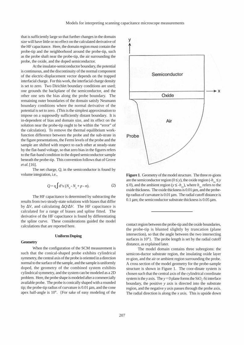
The model domain contains three subregions: thesemicon-ductor substrate region, the insulating oxide layerre-gion, and the air or ambient region surrounding the probe.A cross section of the model geometry for the probe-samplestructure is shown in Figure 1. The coor-dinate system ischosen such that the central axis of the cylindrical coordinatesystem is the y axis. The y = 0 plane forms the SiO
2-Si interface
boundary, the positive y axis is directed into the substrateregion, and the negative y axis passes through the probe axis.The radial direction is along the x axis. This is upside down
(2)
Figure 1. Geometry of the model structure. The three re-gionsare the semiconductor region (0 ≤ y), the oxide region (-h
ox ≤ y
≤ 0), and the ambient region (y ≤ -hox
), where hox
refers to theoxide thickness. The oxide thickness is 0.01 µm, and the probe-tip radius of curvature is 0.01 µm. The radial cutoff distance is0.1 µm; the semiconductor substrate thickness is 0.05 µm.
208
J.F. Marchiando, J.R. Lowney and J.J. Kopanski
from the usual SCM configuration. The semiconductor regionis where y ≥ 0, the oxide region is where -h
ox ≤ y ≤ 0, and the
ambient region is where y ≤ -hox
, where hox
is the oxide layerthickness. The unit of length is expressed in µm, and here, h
ox
= 0.01 µm.The size of the substrate region is set in part by the
radial cutoff distance or length of the x axis. Since the interesthere is to maintain the spatial resolution of the measurementnear that of the probe-tip radius of curvature, the radial cutoffdistance was set to usually 10 times the probe-tip radius ofcurvature. Here, the radial cutoff distance was set to 0.2 µmwhen 1 x 104 µm-3≤ N
a≤ 9 x 104 µm-3; 0.1 µm when 1 x 105 µm-3
≤ Na ≤ 3 x 107 µm-3; and 0.05 µm when 4 x 107 µm-3 ≤ N
a ≤ 1 x 10⁸
µm-3.
The substrate depth (y) cutoff was determined so thatthe substrate region could contain the depletion region, andthe charge neutrality condition could be maintained deepinside the substrate for the given max-imum bias. The maximumbias was roughly set by de-ter-mining when the contour valueof N
a/10 reached the radial cutoff distance.
The length of the probe is determined by using a circulararc to form the outer boundary of the ambient region andrequiring the arc to intersect perpendicularly with theboundaries of the probe and the oxide. Therefore, the probelength is set by the radial cutoff distance. Changing the radialcutoff distance changes the probe length, and for a nonzerobias, this changes the charge on the probe, the net charge inthe semiconductor, and the capacitance. However, when the
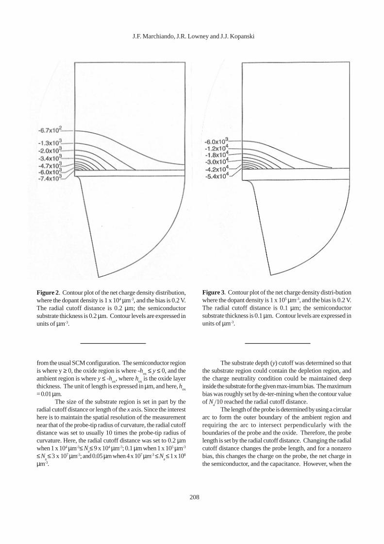
Figure 2. Contour plot of the net charge density distribution,where the dopant density is 1 x 104 µm-3, and the bias is 0.2 V.The radial cutoff distance is 0.2 µm; the semiconductorsubstrate thickness is 0.2 µm. Contour levels are expressed inunits of µm-3.
Figure 3. Contour plot of the net charge density distri-butionwhere the dopant density is 1 x 105 µm-3, and the bias is 0.2 V.The radial cutoff distance is 0.1 µm; the semiconductorsubstrate thickness is 0.1 µm. Contour levels are expressed inunits of µm-3.
Models for interpreting scanning capacitance microscope measurements
209
radial cutoff distance is sufficiently large, the change in thederivative of the high-frequency capacitance is found to besmall and is within the estimated error of the calculation.
This condition, where the calculated derivative of thehigh -frequency capacitance becomes insensitive to changesin the size of the domain, is both important and necessary formodeling an SCM measurement where the objective is todetermine a meaningful absolute measurement and not just arelative measurement. Conversely, for an SCM measurementto be practical, the derivative of the high-frequencycapacitance must be insensitive to and separable from thestray capacitances in the system.
Method of solution
To solve both the nonlinear Poisson equation in thesemiconductor region and the Laplace equation in the ox-ideand the ambient regions, we used PLTMG (Piece-wise LinearTriangular finite-element MultiGrid) [5], a software packagefor solving elliptic partial differential equations for scalar
problems in two dimensions. The package provides supportfor adaptively refining the mesh and for plotting the contoursor the surface profile of the solution or a function of thesolution.
To calculate the capacitance as a function of appliedbias V
B, the depletion region must be suitably meshed to have
an accurate volume integration to find the net charge in thesemiconductor. To help reduce the grid dependence in thecharge calculations, the procedure used here was to find onegrid that would suitably mesh the depletion region at the largestallowed bias setting and then use that mesh for solutions atother smaller biases, starting from deep depletion (V
B > 0) and
mov-ing to accumulation (VB < 0). This is done for each dopant
density considered in the work.Finding a suitable mesh over the maximal depletion
region was difficult. The default adaptive meshing al-gorithmused in PLTMG was found to mesh the region around theprobe-tip in the ambient region quite well, but only at theexpense of the oxide and the substrate regions; they weremeshed too coarsely. Because PLTMG provides little directcontrol of the mesh step size, and the user options for theadaptive meshing al-gorithm are limited, the only way to causePLTMG with-out modification to form a different mesh is toper-turb the equation that PLTMG is trying to solve. Onemethod for improving the mesh was found by: (1) equalizingthe media by setting the relative dielectric constants to one;(2) perturbing the doping profile near the oxide-semi-conductorsurface to force the meshing algorithm to sense thenonuniformity; and (3) solving this perturbed problem at abias of 5 V or 10 V beyond that for the max-imal depletionregion used in the capacitance calcu-lations. Here, theperturbed dopant density is allowed to vary quadratically inthe x direction and decay normally (Gaussian) in the ydirection; the perturbation is localized near the SiO
2-Si
boundary. The perturbation is used only during the meshrefinement procedure; after finding a suitable or muchimproved mesh, the correct equations are solved to find thecapacitance.
The mesh is undoubtedly one source of error in thecalculation. Some error may be expected at larger biases whenthe depletion region penetrates into regions that are lessdensely meshed. Estimating this kind of error with PLTMG isdifficult. One method would involve halving the stepsize ofthe finest mesh, but this is not possible, because PLTMGprovides no option for uniformly refining the finest mesh,unlike for the initial coarse mesh. The only option availablethen is to add points to the mesh. For meshes containing 1 x10⁴ and 2 x 10⁴ points, the derivative high-frequencycapacitance curves were compared and were found to differby less than 0.5% and 3% for low and high dopant densitiesof 1 x 105 µm-3 and 1 x 108 µm-3, respectively. While the numberof mesh points is important, this approach is somewhat opento question, because there is little user control over the
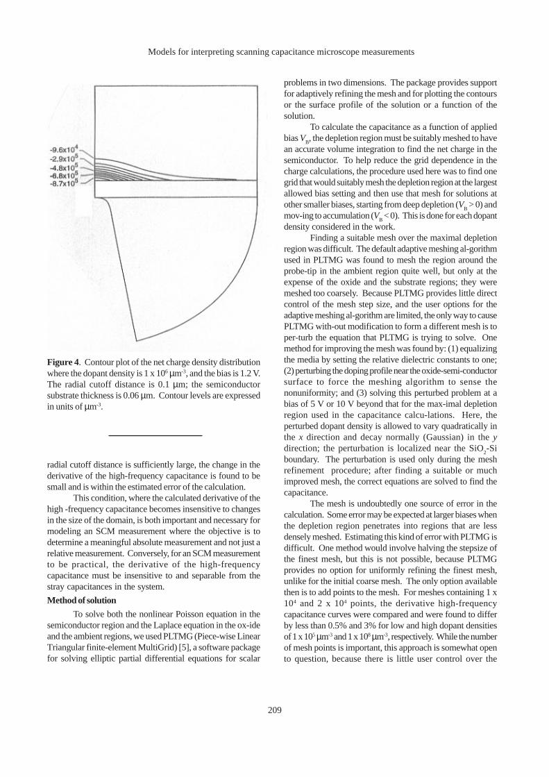
Figure 4. Contour plot of the net charge density distributionwhere the dopant density is 1 x 106 µm-3, and the bias is 1.2 V.The radial cutoff distance is 0.1 µm; the semiconductorsubstrate thickness is 0.06 µm. Contour levels are expressedin units of µm-3.
210
J.F. Marchiando, J.R. Lowney and J.J. Kopanski
placement of the points. However, the results are encouraging.For this work, the meshes used 2 x 10⁴ points.
Another contribution to the error of the calculationinvolves satisfying the boundary conditions. As the bias isincreased above zero, the depletion region forms and expandsalong the SiO
2-Si boundary with a finite skin-depth. At large
biases, the depletion region can expand beyond the radialcutoff distance and move beyond the boundaries of thedomain, and of course, any net charge outside the domain isneglected in the capacitance calculations. The maximum biasused in a capacitance calculation was determined by observingthe depletion region expand along the oxide boundary as afunction of bias until the net number density at the radialcutoff distance became nearly 10% of the dopant density.The HF capacitance and the derivative of the HF capacitancemay be expected to exhibit a larger percentage of this kind oferror at the larger biases. It follows then that the greatestaccuracy and resolution occur when the depletion region issmall, when the bias is small, i.e., near the flat-band condition.
Results of calculations
In order to help interpret capacitance data and themodel accuracy, we show, in Figures 2 through 6, contour
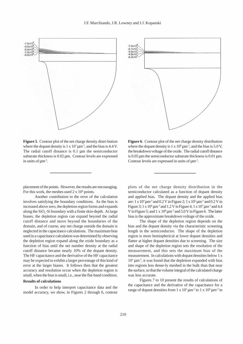
plots of the net charge density distribution in thesemiconductor calculated as a function of dopant densityand applied bias. The dopant density and the applied biasare: 1 x 104 µm-3 and 0.2 V in Figure 2; 1 x 105 µm-3 and 0.2 V inFigure 3; 1 x 106 µm-3 and 1.2 V in Figure 4; 1 x 107 µm-3 and 4.4V in Figure 5; and 1 x 108 µm-3 and 5.0 V in Figure 6. The latterbias is the approximate breakdown voltage of the oxide.
The shape of the depletion region depends on thebias and the dopant density via the characteristic screeninglength in the semiconductor. The shape of the depletionregion is more hemispherical at lower dopant densities andflatter at higher dopant densities due to screening. The sizeand shape of the depletion region sets the resolution of themeasurement, and this sets the maximum bias of themeasurement. In calculations with dopant densities below 1 x105 µm-3, it was found that the depletion expanded with biasinto regions less dense-ly meshed in the bulk than that nearthe surface, so that the volume integral of the calculated chargewas less accurate.
Figures 7 to 10 present the results of calculations ofthe capacitance and the derivative of the capacitance for arange of dopant densities from 1 x 105 µm-3 to 1 x 108 µm-3 in
Figure 5. Contour plot of the net charge density distri-butionwhere the dopant density is 1 x 107 µm-3, and the bias is 4.4 V.The radial cutoff distance is 0.1 µm the semiconductorsubstrate thickness is 0.02 µm. Contour levels are expressedin units of µm-3.
Figure 6. Contour plot of the net charge density distributionwhere the dopant density is 1 x 108 µm-3, and the bias is 5.0 V,the breakdown voltage of the oxide. The radial cutoff distanceis 0.05 µm the semiconductor substrate thickness is 0.01 µm.Contour levels are expressed in units of µm-3.
Models for interpreting scanning capacitance microscope measurements
211
unit increments per decade. Two different values of the radial
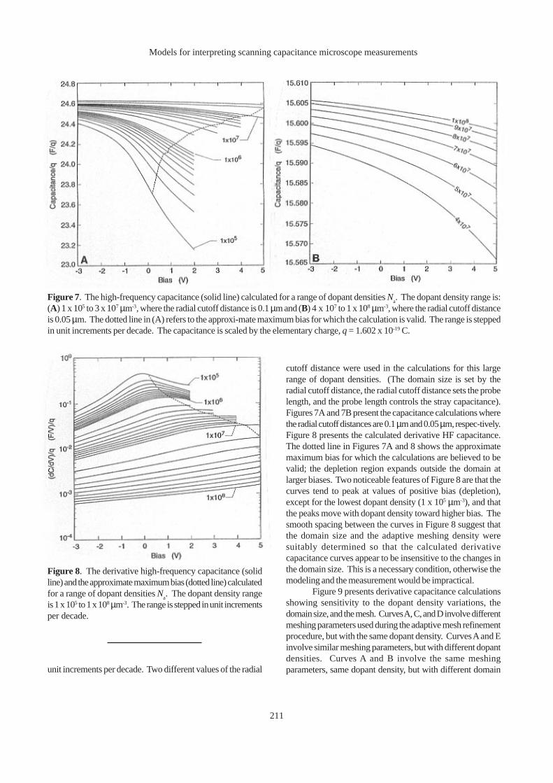
cutoff distance were used in the calculations for this largerange of dopant densities. (The domain size is set by theradial cutoff distance, the radial cutoff distance sets the probelength, and the probe length controls the stray capacitance).Figures 7A and 7B present the capacitance calculations wherethe radial cutoff distances are 0.1 µm and 0.05 µm, respec-tively.Figure 8 presents the calculated derivative HF capacitance.The dotted line in Figures 7A and 8 shows the approximatemaximum bias for which the calculations are believed to bevalid; the depletion region expands outside the domain atlarger biases. Two noticeable features of Figure 8 are that thecurves tend to peak at values of positive bias (depletion),except for the lowest dopant density (1 x 105 µm-3), and thatthe peaks move with dopant density toward higher bias. Thesmooth spacing between the curves in Figure 8 suggest thatthe domain size and the adaptive meshing density weresuitably determined so that the calculated derivativecapacitance curves appear to be insensitive to the changes inthe domain size. This is a necessary condition, otherwise themodeling and the measurement would be impractical.
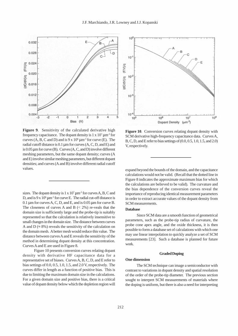
Figure 9 presents derivative capacitance calculationsshowing sensitivity to the dopant density variations, thedomain size, and the mesh. Curves A, C, and D involve differentmeshing parameters used during the adaptive mesh refinementprocedure, but with the same dopant density. Curves A and Einvolve similar meshing parameters, but with different dopantdensities. Curves A and B involve the same meshingparameters, same dopant density, but with different domain
Figure 7. The high-frequency capacitance (solid line) calculated for a range of dopant densities Na. The dopant density range is:
(A) 1 x 10⁵ to 3 x 107 µm-3, where the radial cutoff distance is 0.1 µm and (B) 4 x 10⁷ to 1 x 108 µm-3, where the radial cutoff distanceis 0.05 µm. The dotted line in (A) refers to the approxi-mate maximum bias for which the calculation is valid. The range is steppedin unit increments per decade. The capacitance is scaled by the elementary charge, q = 1.602 x 10⁻¹⁹ C.
Figure 8. The derivative high-frequency capacitance (solidline) and the approximate maximum bias (dotted line) calculatedfor a range of dopant densities N
a. The dopant density range
is 1 x 10⁵ to 1 x 108 µm-3. The range is stepped in unit incrementsper decade.
212
J.F. Marchiando, J.R. Lowney and J.J. Kopanski
sizes. The dopant density is 1 x 107 µm-3 for curves A, B, C andD, and is 9 x 106 µm-3 for curve E. The radial cut-off distance is0.1 µm for curves A, C, D, and E, and is 0.05 µm for curve B.The closeness of curves A and B (< 2%) re-veals that thedomain size is sufficiently large and the probe-tip is suitablyrepresented so that the calculation is relatively insensitive tosmall changes in the domain size. The distance between curvesA and D (≈ 8%) reveals the sensitivity of the calculation onthe domain mesh. A better mesh would reduce this value. Thedistance between curves A and E reveals the sensitivity of themethod in determining dopant density at this concentration.Curves A and E are used in Figure 8.
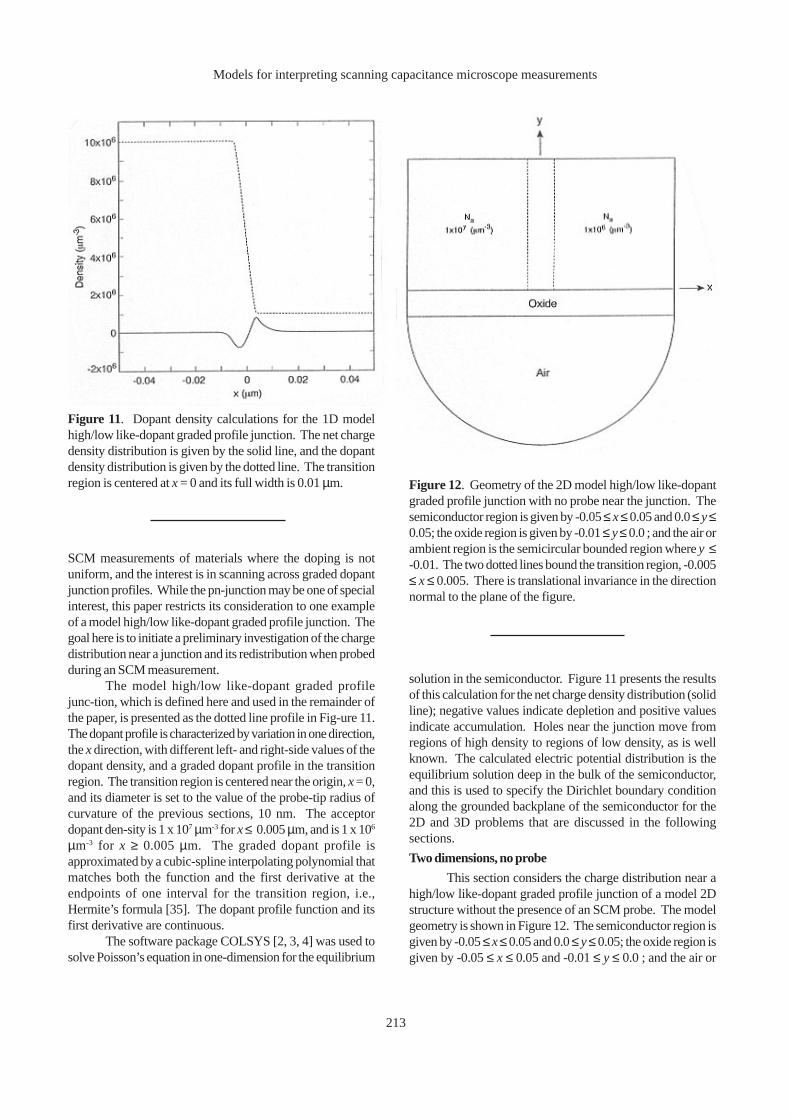
Figure 10 presents conversion curves relating dopantdensity with derivative HF capacitance data for arepresentative set of biases. Curves A, B, C, D, and E refer tobias settings of 0.0, 0.5, 1.0, 1.5, and 2.0 V, respectively. Thecurves differ in length as a function of positive bias. This isdue to limiting the maximum domain size in the calculations.For a given domain size and positive bias, there is a criticalvalue of dopant density below which the depletion region will
expand beyond the bounds of the domain, and the capacitancecalculations would not be valid. (Recall that the dotted line inFigure 8 indicates the approximate maximum bias for whichthe calculations are believed to be valid). The curvature andthe bias dependence of the conversion curves reveal theimportance of reproducing identical measurement parametersin order to extract accurate values of the dopant density fromSCM measurements.
Database
Since SCM data are a smooth function of geometricalparameters, such as the probe-tip radius of curvature, theprobe cone apex angle, and the oxide thickness, it is thenpossible to form a database set of calculations with which onemay use linear interpolation to quickly analyze a set of SCMmeasurements [23]. Such a database is planned for futurework.
Graded Doping
One dimension
The SCM technique can image a semiconductor withcontrast to variations in dopant density and spatial resolutionof the order of the probe-tip diameter. The previous sectionsought to interpret SCM measurements of materials wherethe doping is uniform, but there is also a need for interpreting
Figure 9. Sensitivity of the calculated derivative highfrequency capacitance. The dopant density is 1 x 107 µm-3 forcurves (A, B, C and D) and is 9 x 106 µm-3 for curve (E). Theradial cutoff distance is 0.1 µm for curves (A, C, D, and E) andis 0.05 µm for curve (B). Curves (A, C, and D) involve differentmeshing parameters, but the same dopant density; curves (Aand E) involve similar meshing parameters, but different dopantdensities; and curves (A and B) involve different radial cutoffvalues.
Figure 10. Conversion curves relating dopant density withSCM derivative high-frequency capacitance data. Curves A,B, C, D, and E refer to bias settings of (0.0, 0.5, 1.0, 1.5, and 2.0)V, respectively.
Models for interpreting scanning capacitance microscope measurements
213
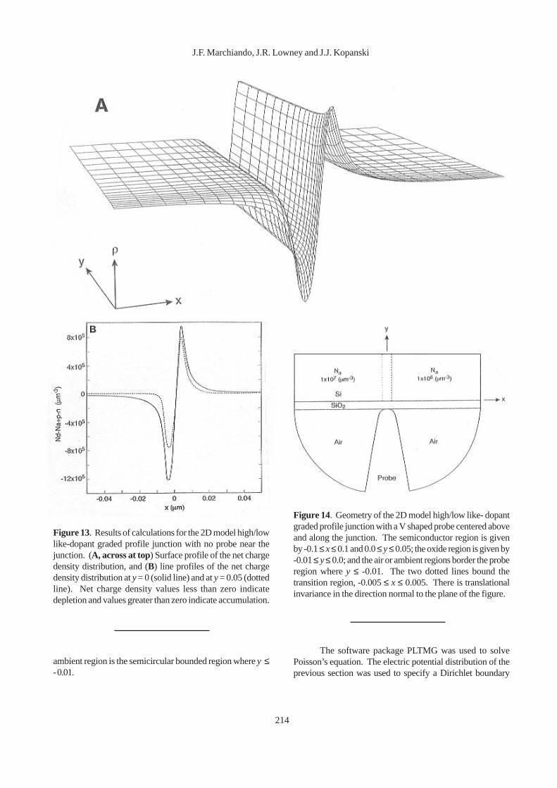
SCM measurements of materials where the doping is notuniform, and the interest is in scanning across graded dopantjunction profiles. While the pn-junction may be one of specialinterest, this paper restricts its consideration to one exampleof a model high/low like-dopant graded profile junction. Thegoal here is to initiate a preliminary investigation of the chargedistribution near a junction and its redistribution when probedduring an SCM measurement.
The model high/low like-dopant graded profilejunc-tion, which is defined here and used in the remainder ofthe paper, is presented as the dotted line profile in Fig-ure 11.The dopant profile is characterized by variation in one direction,the x direction, with different left- and right-side values of thedopant density, and a graded dopant profile in the transitionregion. The transition region is centered near the origin, x = 0,and its diameter is set to the value of the probe-tip radius ofcurvature of the previous sections, 10 nm. The acceptordopant den-sity is 1 x 107 µm-3 for x ≤ 0.005 µm, and is 1 x 10⁶
µm-3 for x ≥ 0.005 µm. The graded dopant profile isapproximated by a cubic-spline interpolating polynomial thatmatches both the function and the first derivative at theendpoints of one interval for the transition region, i.e.,Hermite’s formula [35]. The dopant profile function and itsfirst derivative are continuous.
The software package COLSYS [2, 3, 4] was used tosolve Poisson’s equation in one-dimension for the equilibrium
solution in the semiconductor. Figure 11 presents the resultsof this calculation for the net charge density distribution (solidline); negative values indicate depletion and positive valuesindicate accumulation. Holes near the junction move fromregions of high density to regions of low density, as is wellknown. The calculated electric potential distribution is theequilibrium solution deep in the bulk of the semiconductor,and this is used to specify the Dirichlet boundary conditionalong the grounded backplane of the semiconductor for the2D and 3D problems that are discussed in the followingsections.
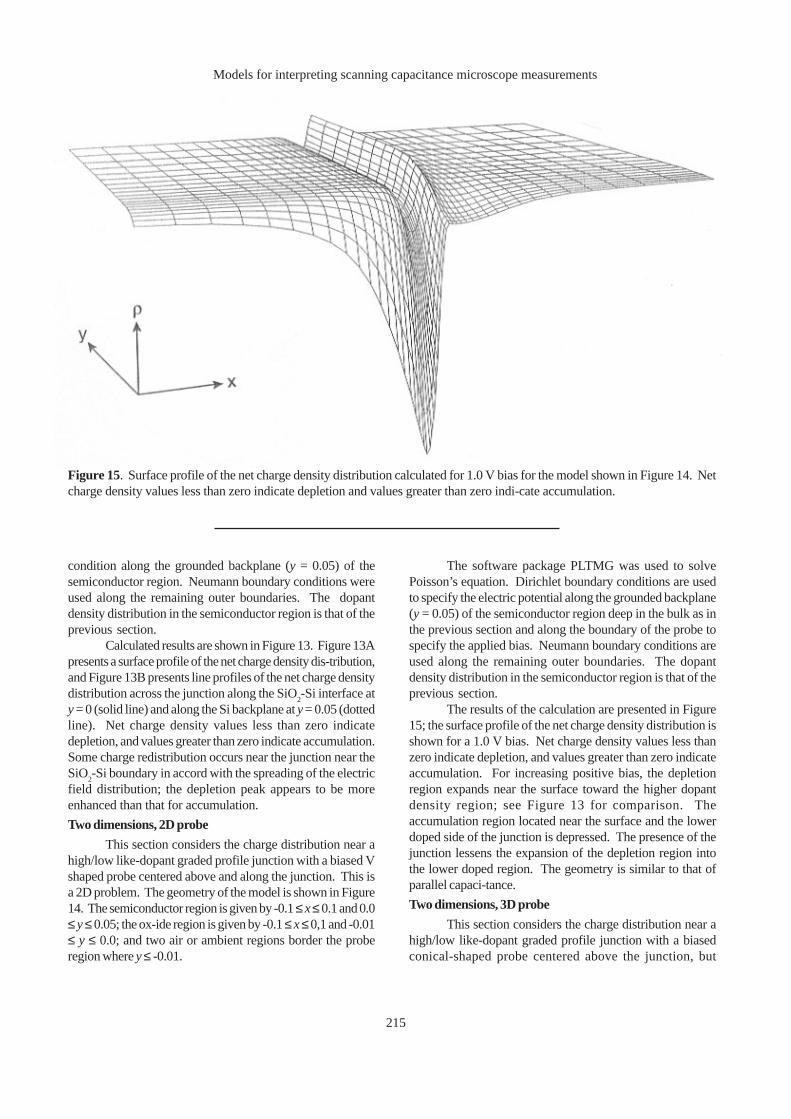
Two dimensions, no probe
This section considers the charge distribution near ahigh/low like-dopant graded profile junction of a model 2Dstructure without the presence of an SCM probe. The modelgeometry is shown in Figure 12. The semiconductor region isgiven by -0.05 ≤ x ≤ 0.05 and 0.0 ≤ y ≤ 0.05; the oxide region isgiven by -0.05 ≤ x ≤ 0.05 and -0.01 ≤ y ≤ 0.0 ; and the air or
Figure 11. Dopant density calculations for the 1D modelhigh/low like-dopant graded profile junction. The net chargedensity distribution is given by the solid line, and the dopantdensity distribution is given by the dotted line. The transitionregion is centered at x = 0 and its full width is 0.01 µm. Figure 12. Geometry of the 2D model high/low like-dopant
graded profile junction with no probe near the junction. Thesemiconductor region is given by -0.05 ≤ x ≤ 0.05 and 0.0 ≤ y ≤0.05; the oxide region is given by -0.01 ≤ y ≤ 0.0 ; and the air orambient region is the semicircular bounded region where y ≤-0.01. The two dotted lines bound the transition region, -0.005≤ x ≤ 0.005. There is translational invariance in the directionnormal to the plane of the figure.
214
J.F. Marchiando, J.R. Lowney and J.J. Kopanski
ambient region is the semicircular bounded region where y ≤- 0.01.
The software package PLTMG was used to solvePoisson’s equation. The electric potential distribution of theprevious section was used to specify a Dirichlet boundary
Figure 13. Results of calculations for the 2D model high/lowlike-dopant graded profile junction with no probe near thejunction. (A, across at top) Surface profile of the net chargedensity distribution, and (B) line profiles of the net chargedensity distribution at y = 0 (solid line) and at y = 0.05 (dottedline). Net charge density values less than zero indicatedepletion and values greater than zero indicate accumulation.
Figure 14. Geometry of the 2D model high/low like- dopantgraded profile junction with a V shaped probe centered aboveand along the junction. The semiconductor region is givenby -0.1 ≤ x ≤ 0.1 and 0.0 ≤ y ≤ 0.05; the oxide region is given by-0.01 ≤ y ≤ 0.0; and the air or ambient regions border the proberegion where y ≤ -0.01. The two dotted lines bound thetransition region, -0.005 ≤ x ≤ 0.005. There is translationalinvariance in the direction normal to the plane of the figure.
Models for interpreting scanning capacitance microscope measurements
215
condition along the grounded backplane (y = 0.05) of thesemiconductor region. Neumann boundary conditions wereused along the remaining outer boundaries. The dopantdensity distribution in the semiconductor region is that of theprevious section.
Calculated results are shown in Figure 13. Figure 13Apresents a surface profile of the net charge density dis-tribution,and Figure 13B presents line profiles of the net charge densitydistribution across the junction along the SiO
2-Si interface at
y = 0 (solid line) and along the Si backplane at y = 0.05 (dottedline). Net charge density values less than zero indicatedepletion, and values greater than zero indicate accumulation.Some charge redistribution occurs near the junction near theSiO
2-Si boundary in accord with the spreading of the electric
field distribution; the depletion peak appears to be moreenhanced than that for accumulation.
Two dimensions, 2D probe
This section considers the charge distribution near ahigh/low like-dopant graded profile junction with a biased Vshaped probe centered above and along the junction. This isa 2D problem. The geometry of the model is shown in Figure14. The semiconductor region is given by -0.1 ≤ x ≤ 0.1 and 0.0≤ y ≤ 0.05; the ox-ide region is given by -0.1 ≤ x ≤ 0,1 and -0.01≤ y ≤ 0.0; and two air or ambient regions border the proberegion where y ≤ -0.01.
The software package PLTMG was used to solvePoisson’s equation. Dirichlet boundary conditions are usedto specify the electric potential along the grounded backplane(y = 0.05) of the semiconductor region deep in the bulk as inthe previous section and along the boundary of the probe tospecify the applied bias. Neumann boundary conditions areused along the remaining outer boundaries. The dopantdensity distribution in the semiconductor region is that of theprevious section.
The results of the calculation are presented in Figure15; the surface profile of the net charge density distribution isshown for a 1.0 V bias. Net charge density values less thanzero indicate depletion, and values greater than zero indicateaccumulation. For increasing positive bias, the depletionregion expands near the surface toward the higher dopantdensity region; see Figure 13 for comparison. Theaccumulation region located near the surface and the lowerdoped side of the junction is depressed. The presence of thejunction lessens the expansion of the depletion region intothe lower doped region. The geometry is similar to that ofparallel capaci-tance.
Two dimensions, 3D probe
This section considers the charge distribution near ahigh/low like-dopant graded profile junction with a biasedconical-shaped probe centered above the junction, but
Figure 15. Surface profile of the net charge density distribution calculated for 1.0 V bias for the model shown in Figure 14. Netcharge density values less than zero indicate depletion and values greater than zero indi-cate accumulation.
216
J.F. Marchiando, J.R. Lowney and J.J. Kopanski
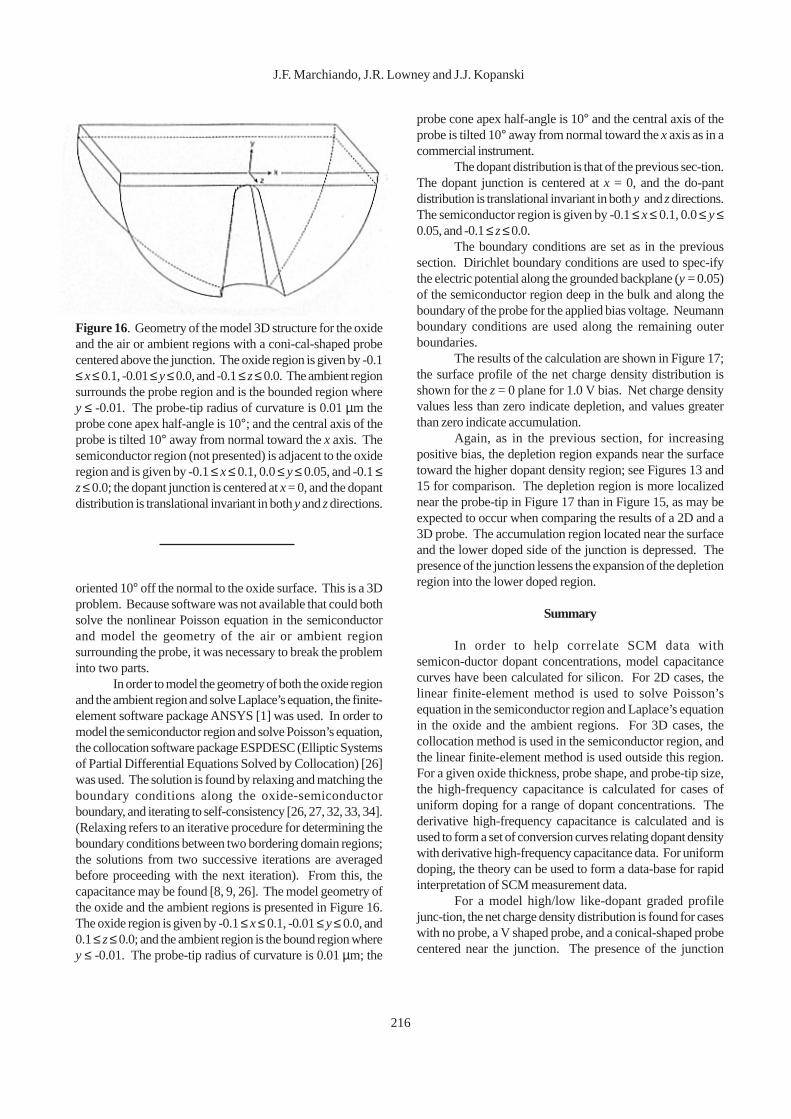
oriented 10° off the normal to the oxide surface. This is a 3Dproblem. Because software was not available that could bothsolve the nonlinear Poisson equation in the semiconductorand model the geometry of the air or ambient regionsurrounding the probe, it was necessary to break the probleminto two parts.
In order to model the geometry of both the oxide regionand the ambient region and solve Laplace’s equation, the finite-element software package ANSYS [1] was used. In order tomodel the semiconductor region and solve Poisson’s equation,the collocation software package ESPDESC (Elliptic Systemsof Partial Differential Equations Solved by Collocation) [26]was used. The solution is found by relaxing and matching theboundary conditions along the oxide-semiconductorboundary, and iterating to self-consistency [26, 27, 32, 33, 34].(Relaxing refers to an iterative procedure for determining theboundary conditions between two bordering domain regions;the solutions from two successive iterations are averagedbefore proceeding with the next iteration). From this, thecapacitance may be found [8, 9, 26]. The model geometry ofthe oxide and the ambient regions is presented in Figure 16.The oxide region is given by -0.1 ≤ x ≤ 0.1, -0.01 ≤ y ≤ 0.0, and0.1 ≤ z ≤ 0.0; and the ambient region is the bound region wherey ≤ -0.01. The probe-tip radius of curvature is 0.01 µm; the
probe cone apex half-angle is 10° and the central axis of theprobe is tilted 10° away from normal toward the x axis as in acommercial instrument.
The dopant distribution is that of the previous sec-tion.The dopant junction is centered at x = 0, and the do-pantdistribution is translational invariant in both y and z directions.The semiconductor region is given by -0.1 ≤ x ≤ 0.1, 0.0 ≤ y ≤0.05, and -0.1 ≤ z ≤ 0.0.
The boundary conditions are set as in the previoussection. Dirichlet boundary conditions are used to spec-ifythe electric potential along the grounded backplane (y = 0.05)of the semiconductor region deep in the bulk and along theboundary of the probe for the applied bias voltage. Neumannboundary conditions are used along the remaining outerboundaries.
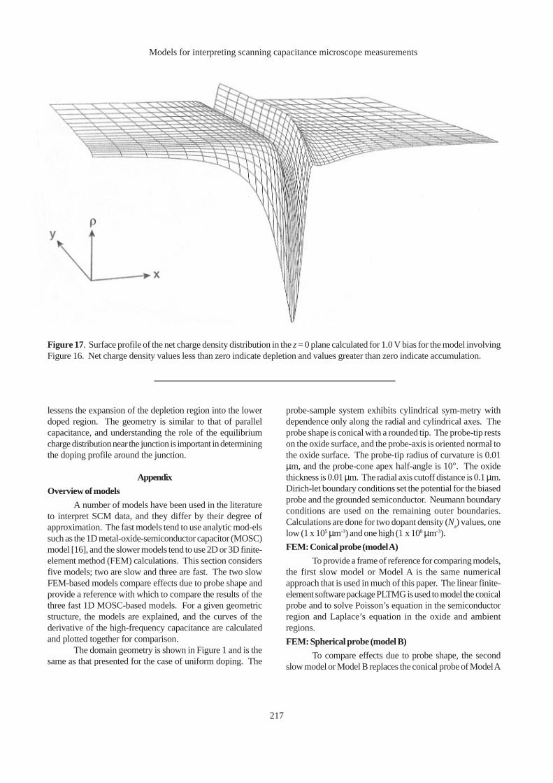
The results of the calculation are shown in Figure 17;the surface profile of the net charge density distribution isshown for the z = 0 plane for 1.0 V bias. Net charge densityvalues less than zero indicate depletion, and values greaterthan zero indicate accumulation.
Again, as in the previous section, for increasingpositive bias, the depletion region expands near the surfacetoward the higher dopant density region; see Figures 13 and15 for comparison. The depletion region is more localizednear the probe-tip in Figure 17 than in Figure 15, as may beexpected to occur when comparing the results of a 2D and a3D probe. The accumulation region located near the surfaceand the lower doped side of the junction is depressed. Thepresence of the junction lessens the expansion of the depletionregion into the lower doped region.
Summary
In order to help correlate SCM data withsemicon-ductor dopant concentrations, model capacitancecurves have been calculated for silicon. For 2D cases, thelinear finite-element method is used to solve Poisson’sequation in the semiconductor region and Laplace’s equationin the oxide and the ambient regions. For 3D cases, thecollocation method is used in the semiconductor region, andthe linear finite-element method is used outside this region.For a given oxide thickness, probe shape, and probe-tip size,the high-frequency capacitance is calculated for cases ofuniform doping for a range of dopant concentrations. Thederivative high-frequency capacitance is calculated and isused to form a set of conversion curves relating dopant densitywith derivative high-frequency capacitance data. For uniformdoping, the theory can be used to form a data-base for rapidinterpretation of SCM measurement data.
For a model high/low like-dopant graded profilejunc-tion, the net charge density distribution is found for caseswith no probe, a V shaped probe, and a conical-shaped probecentered near the junction. The presence of the junction
Figure 16. Geometry of the model 3D structure for the oxideand the air or ambient regions with a coni-cal-shaped probecentered above the junction. The oxide region is given by -0.1≤ x ≤ 0.1, -0.01 ≤ y ≤ 0.0, and -0.1 ≤ z ≤ 0.0. The ambient regionsurrounds the probe region and is the bounded region wherey ≤ -0.01. The probe-tip radius of curvature is 0.01 µm theprobe cone apex half-angle is 10°; and the central axis of theprobe is tilted 10° away from normal toward the x axis. Thesemiconductor region (not presented) is adjacent to the oxideregion and is given by -0.1 ≤ x ≤ 0.1, 0.0 ≤ y ≤ 0.05, and -0.1 ≤z ≤ 0.0; the dopant junction is centered at x = 0, and the dopantdistribution is translational invariant in both y and z directions.
Models for interpreting scanning capacitance microscope measurements
217
lessens the expansion of the depletion region into the lowerdoped region. The geometry is similar to that of parallelcapacitance, and understanding the role of the equilibriumcharge distribution near the junction is important in determiningthe doping profile around the junction.
Appendix
Overview of models
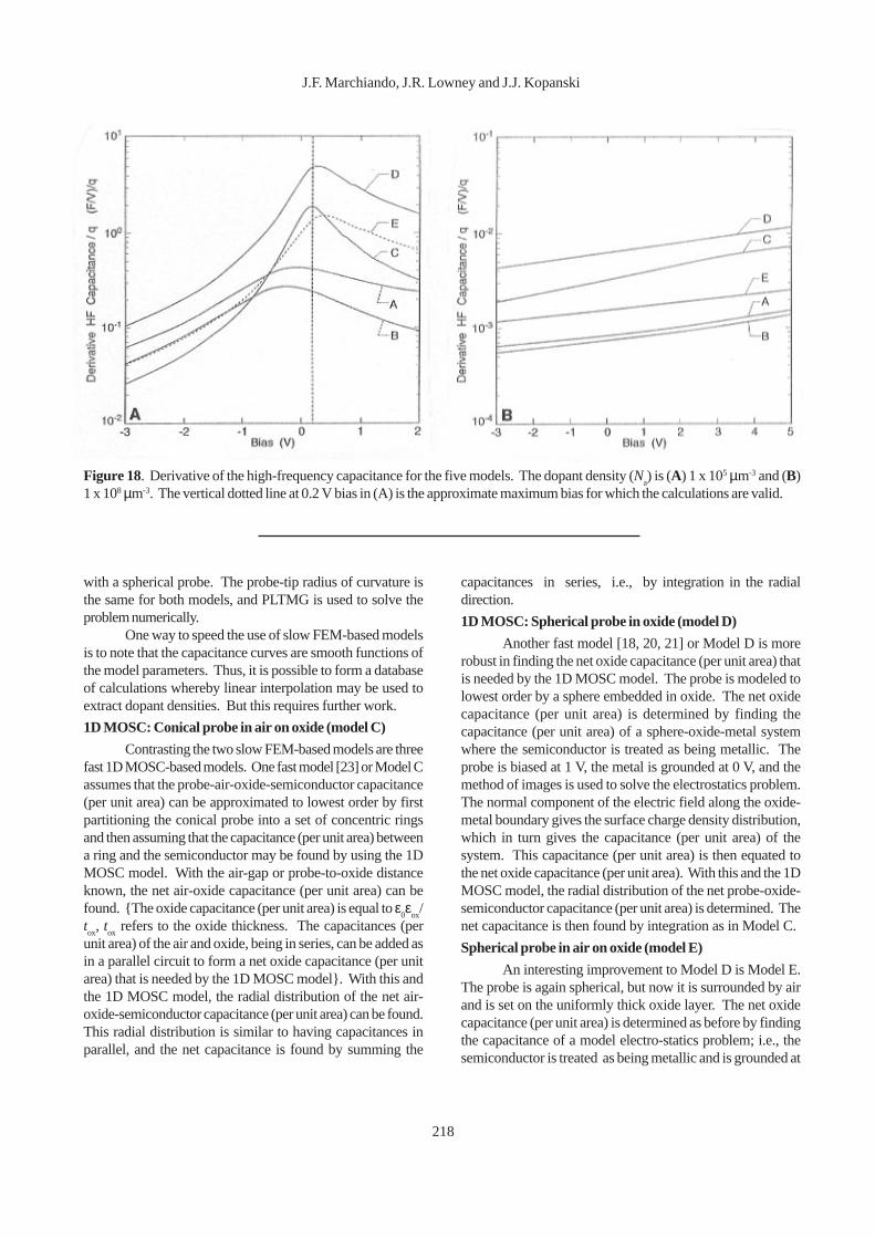
A number of models have been used in the literatureto interpret SCM data, and they differ by their degree ofapproximation. The fast models tend to use analytic mod-elssuch as the 1D metal-oxide-semiconductor capacitor (MOSC)model [16], and the slower models tend to use 2D or 3D finite-element method (FEM) calculations. This section considersfive models; two are slow and three are fast. The two slowFEM-based models compare effects due to probe shape andprovide a reference with which to compare the results of thethree fast 1D MOSC-based models. For a given geometricstructure, the models are explained, and the curves of thederivative of the high-frequency capacitance are calculatedand plotted together for comparison.
The domain geometry is shown in Figure 1 and is thesame as that presented for the case of uniform doping. The
probe-sample system exhibits cylindrical sym-metry withdependence only along the radial and cylindrical axes. Theprobe shape is conical with a rounded tip. The probe-tip restson the oxide surface, and the probe-axis is oriented normal tothe oxide surface. The probe-tip radius of curvature is 0.01µm, and the probe-cone apex half-angle is 10°. The oxidethickness is 0.01 µm. The radial axis cutoff distance is 0.1 µm.Dirich-let boundary conditions set the potential for the biasedprobe and the grounded semiconductor. Neumann boundaryconditions are used on the remaining outer boundaries.Calculations are done for two dopant density (N
a) values, one
low (1 x 105 µm-3) and one high (1 x 108 µm-3).
FEM: Conical probe (model A)
To provide a frame of reference for comparing models,the first slow model or Model A is the same numericalapproach that is used in much of this paper. The linear finite-element software package PLTMG is used to model the conicalprobe and to solve Poisson’s equation in the semiconductorregion and Laplace’s equation in the oxide and ambientregions.
FEM: Spherical probe (model B)
To compare effects due to probe shape, the secondslow model or Model B replaces the conical probe of Model A
Figure 17. Surface profile of the net charge density distribution in the z = 0 plane calculated for 1.0 V bias for the model involvingFigure 16. Net charge density values less than zero indicate depletion and values greater than zero indicate accumulation.
218
J.F. Marchiando, J.R. Lowney and J.J. Kopanski
with a spherical probe. The probe-tip radius of curvature isthe same for both models, and PLTMG is used to solve theproblem numerically.
One way to speed the use of slow FEM-based modelsis to note that the capacitance curves are smooth functions ofthe model parameters. Thus, it is possible to form a databaseof calculations whereby linear interpolation may be used toextract dopant densities. But this requires further work.
1D MOSC: Conical probe in air on oxide (model C)
Contrasting the two slow FEM-based models are threefast 1D MOSC-based models. One fast model [23] or Model Cassumes that the probe-air-oxide-semiconductor capacitance(per unit area) can be approximated to lowest order by firstpartitioning the conical probe into a set of concentric ringsand then assuming that the capacitance (per unit area) betweena ring and the semiconductor may be found by using the 1DMOSC model. With the air-gap or probe-to-oxide distanceknown, the net air-oxide capacitance (per unit area) can befound. {The oxide capacitance (per unit area) is equal to ε
0ε
ox/
tox
, tox
refers to the oxide thickness. The capacitances (perunit area) of the air and oxide, being in series, can be added asin a parallel circuit to form a net oxide capacitance (per unitarea) that is needed by the 1D MOSC model}. With this andthe 1D MOSC model, the radial distribution of the net air-oxide-semiconductor capacitance (per unit area) can be found.This radial distribution is similar to having capacitances inparallel, and the net capacitance is found by summing the
capacitances in series, i.e., by integration in the radialdirection.
1D MOSC: Spherical probe in oxide (model D)
Another fast model [18, 20, 21] or Model D is morerobust in finding the net oxide capacitance (per unit area) thatis needed by the 1D MOSC model. The probe is modeled tolowest order by a sphere embedded in oxide. The net oxidecapacitance (per unit area) is determined by finding thecapacitance (per unit area) of a sphere-oxide-metal systemwhere the semiconductor is treated as being metallic. Theprobe is biased at 1 V, the metal is grounded at 0 V, and themethod of images is used to solve the electrostatics problem.The normal component of the electric field along the oxide-metal boundary gives the surface charge density distribution,which in turn gives the capacitance (per unit area) of thesystem. This capacitance (per unit area) is then equated tothe net oxide capacitance (per unit area). With this and the 1DMOSC model, the radial distribution of the net probe-oxide-semiconductor capacitance (per unit area) is determined. Thenet capacitance is then found by integration as in Model C.
Spherical probe in air on oxide (model E)
An interesting improvement to Model D is Model E.The probe is again spherical, but now it is surrounded by airand is set on the uniformly thick oxide layer. The net oxidecapacitance (per unit area) is determined as before by findingthe capacitance of a model electro-statics problem; i.e., thesemiconductor is treated as being metallic and is grounded at
Figure 18. Derivative of the high-frequency capacitance for the five models. The dopant density (Na) is (A) 1 x 105 µm-3 and (B)
1 x 108 µm-3. The vertical dotted line at 0.2 V bias in (A) is the approximate maximum bias for which the calculations are valid.
Models for interpreting scanning capacitance microscope measurements
219
0 V, and the sphere is biased at 1 V. While a method of imagessolution would be needed here to qualify it as a fast method,we used PLTMG to find the normal component of the electricfield along the oxide-metal boundary. This gives the surfacecharge density distribution, which in turn gives the radialdistribution of the net oxide capacitance (per unit area). The1D MOSC is used as before in Model D to find the netcapacitance.
Results and comparisons of models
Figure 18 shows the derivative of the high-frequencycapacitance of the five models, where the dopant densities N
a
are 1 x 105 µm-3 (Fig. 18A) and 1 x 108 µm-3 (Fig. 18B). Thevertical dotted line at bias 0.2 V in Figure 18A is the approximatemaximum bias for which the calculations are valid. At largerbias, the depletion region expands beyond the set boundariesof the domain region, and the net charge that is outside theset boundaries is not included in the calculation of thecapacitance. (The domain size is set, in part, by the radialcutoff distance, and this is determined subjectively asexplained in the section entitled Geometry under the mainheading Uniform Doping. Here, the radial cutoff distances are0.1 µm and 0.05 µm for dopant densities 1 x 105 µm-3 and 1 x 10⁸
µm-3, respectively).The degree of agreement (comparative scaling) of the
results of the fast 1D MOSC-based models and the slow FEM-based models may be expected to depend, in part, on thedegree to which the assumptions of the 1D MOSC model are
satisfied. The best agreement may be expected at high dopantdensities where the screening length is small compared to theprobe-tip radius of curvature and the oxide thickness. Theworst agreement may be expected at low dopant densitieswhere the screening length is large compared to the probe-tipradius of curvature and the oxide thickness.
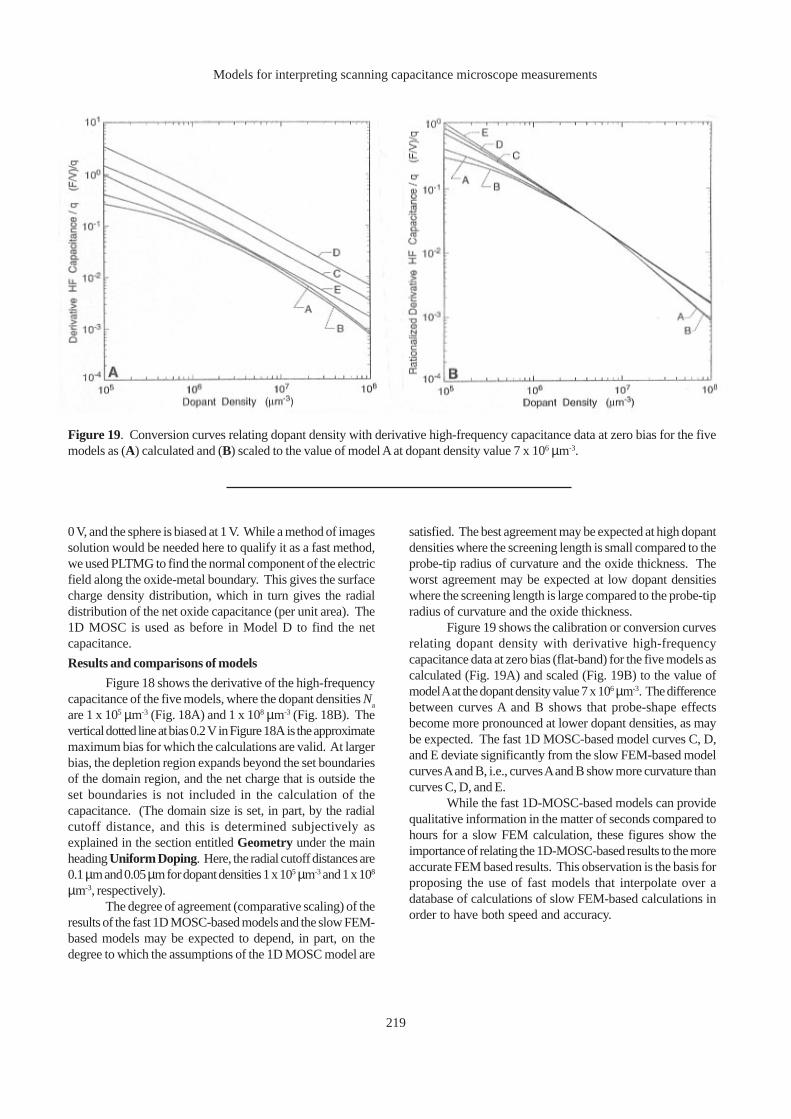
Figure 19 shows the calibration or conversion curvesrelating dopant density with derivative high-frequencycapacitance data at zero bias (flat-band) for the five models ascalculated (Fig. 19A) and scaled (Fig. 19B) to the value ofmodel A at the dopant density value 7 x 106 µm-3. The differencebetween curves A and B shows that probe-shape effectsbecome more pronounced at lower dopant densities, as maybe expected. The fast 1D MOSC-based model curves C, D,and E deviate significantly from the slow FEM-based modelcurves A and B, i.e., curves A and B show more curvature thancurves C, D, and E.
While the fast 1D-MOSC-based models can providequalitative information in the matter of seconds compared tohours for a slow FEM calculation, these figures show theimportance of relating the 1D-MOSC-based results to the moreaccurate FEM based results. This observation is the basis forproposing the use of fast models that interpolate over adatabase of calculations of slow FEM-based calculations inorder to have both speed and accuracy.
Figure 19. Conversion curves relating dopant density with derivative high-frequency capacitance data at zero bias for the fivemodels as (A) calculated and (B) scaled to the value of model A at dopant density value 7 x 106 µm-3.
220
J.F. Marchiando, J.R. Lowney and J.J. Kopanski
Acknowledgments
It is a pleasure to acknowledge those at NIST whohelped us to accomplish this work. They include: Dr. David G.Seiler for his concern regarding semiconductor characterizationmodeling that led to this project, Dr. Ronald F. Boisvert for hisassistance with the software libraries [10, 12, 13], Dr. William F.Mitchell for his assistance with the PLTMG software packageand the many helpful discussions, Drs. Hai C. Tang, Jeffrey T.Fong and Mrs. P. Darcy Barnett for their assistance with theANSYS software package, Mr. N. Alan Heckert for hisassistance with the NCAR graphics package, Dr. James S.Sims for his assistance with providing machine time forcalculations, Mr. Denis A. Lehane for computer operatingsystem support, and Mr. Raymond J. Mele for his graphics artwork.
This work was supported in part by the NationalSemiconductor Metrology Program at the National Instituteof Standards and Technology (NIST); not subject to copyright.Certain software are identified in this paper to adequatelyspecify the modeling pro-cedures. Such identification doesnot imply recommendation or endorsement by the NIST, nordoes it imply that the methods identified are necessarily thebest available for the purpose.
References
[1] ANSYS (1994) ANSYS user’s manual for revision5.1. Vol. 1: Procedures. ANSYS, Inc., 201 Johnson Road,Houston, PA. Chapter 4, 9-15.
[2] Ascher U, Christiansen J, Russell RD (1981)Collocation software for boundary-value ODEs. ACM TransMath Softw 7: 209-222.
[3] Ascher U, Christiansen J, Russell RD (1981)Algorithm 569, COLSYS: Collocation software for boundary-value ODEs. ACM Trans Math Softw 7: 223-229.
[4] Bader G, Ascher U (1987) A new basisimplementation for a mixed order boundary value ODE solver.SIAM J Sci Stat Comput 8: 483-500.
[5] Bank RE (1994) PLTMG: A software package forsolving elliptic partial differential equations, users’ guide 7.0.Society for Industrial and Applied Mathematics. Philadelphia,PA. Software is available at URL: http://www.netlib.org/.
[6] Barber HD (1967) Effective mass and intrinsiccon-centration in silicon. Solid-State Electron 10: 1039-1051.
[7] Barrett RC, Quate CF (1991) Charge storage in anitride-oxide-silicon medium by scanning capacitancemicroscopy. J Appl Phys 70: 2725-2733.
[8] Berntsen J, Espelid TO, Genz A (1991) An adaptivealgorithm for the approximate calculation of multiple integrals.ACM Trans Math Softw 17: 437-451.
[9] Berntsen J, Espelid TO, Genz A (1991) Algorithm698, DCUHRE: An adaptive multidimensional integration
routine for a vector of integrals. ACM Trans Math Softw 17:452-456.
[10] Boisvert RF, Howe SE, Kahaner DK, SpringmannJL (1990) Guide to Available Mathematical Software, NISTIR90-4237. Center for Computing and Applied Mathematics,National Institute of Standards and Technology (NIST),Gaithersburg, MD (U.S. Department of Commerce). Availablefrom: Mathematical and Computational Sciences Divisionwithin the Information Technology Laboratory of the NIST.Also available at URL: http://math.nist.gov/gams/.
[11] Diebold AC, Kump MR, Kopanski JJ, Seiler DG(1996) Characterization of two-dimensional dopant profiles:Status and review. J Vac Sci Technol B 14: 196-201.
[12] Dongarra JJ, Grosse E (1987) Distribution ofmathematical software via electronic mail. Comm ACM 30:403-407.
[13] Dongarra J, Rowan T, Wade R (1995) Softwaredistribution using Xnetlib. ACM Trans Math Softw 21: 79-88.
[14] Dreyer M, Wiesendanger R (1995) Scanningcapacitance microscopy and spectroscopy applied to localcharge modifications and characterizations of nitride-oxide-silicon heterostructures. Appl Phys A 61: 357-362.
[15] Gaitan M, Mayergoyz ID (1989) A numericalanal-ysis for the small-signal response of the MOS capacitor.Solid-State Electron 32: 207-213.
[16] Grove AS, Deal BE, Snow EH, Sah CT (1965)Investigation of thermally oxidised silicon surfaces usingmetal-oxide-semiconductor structures. Solid-State Electron 8:145-163.
[17] Halen PV, Pulfrey DL (1985) Accurate, short seriesapproximations to Fermi-Dirac integrals of order 1/2, 1/2, 1, 3/2, 5/2, 3, and 7/2. J Appl Phys 57: 5271-5274. Erratum. J ApplPhys 59: 2264-2265.
[18] Huang Y (1995) Quantitative two-dimensionaldopant profile measurement on semiconductors by scanningprobe microscopy. Doctoral Dissertation. Department ofPhysics, University of Utah, Salt Lake City, UT. pp. 42-60.
[19] Huang Y, Williams CC (1994) Capacitance-voltagemeasurement and modeling on a nanometer scale by scanningC V microscopy. J Vac Sci Technol B 12: 369-372.
[20] Huang Y, Williams CC, Slinkman J (1995)Quantitative two-dimensional dopant profile measurement andinverse modeling by scanning capacitance microscopy. ApplPhys Lett 66: 344-346.
[21] Huang Y, Williams CC, Smith H (1996) Directcomparison of cross-sectional scanning capacitancemicroscope dopant profile and vertical secondary ion-massspectroscopy profile. J Vac Sci Technol B 14: 433-436.
[22] Johnson WC, Panousis PT (1971) The influenceof Debye length on the C-V measurement of doping profiles.IEEE Trans Electron Devices 18: 965-973.
[23] Kopanski JJ, Marchiando JF, Lowney JR (1997)Scanning capacitance microscopy applied to two-dimensional
Models for interpreting scanning capacitance microscope measurements
221
dopant profiling of semiconductors. Mater Sci Eng B 44:46-51.
[24] Kopanski JJ, Marchiando JF, Lowney JR (1996)Scanning capacitance microscopy measurements andmodeling for dopant profiling in silicon. In: Semi-conductorCharacterization: Present Status and Future Needs. Bullis WM,Seiler DG, Diebold AC (eds.). AIP Press, Woodbury, NY. pp.308-312.
[25] Kopanski JJ, Marchiando JF, Lowney JR (1996)Scanning capacitance microscopy measurements andmodeling: Progress towards dopant profiling of silicon. J VacSci Technol B 14: 242-247.
[26] Marchiando JF (1996) Application of the collocationmethod in three dimensions to a model semiconductor problem.Int J Num Meth Eng 39: 1029-1040. {The long version appearsin (1995) On using collocation in three dimensions and solvinga model semiconductor problem. J Res Natl Inst Stand Technol100: 661-675.}
[27] McFaddin HS, Rice JR (1992) Collaborating PDEsolvers. Applied Numerical Math 10: 279-295.
[28] Morgan SP, Smits FM (1960) Potential distributionand capacitance of a graded p-n junction. Bell Sys Tech J 39:1573-1602.
[29] Neubauer G, Erickson A, Williams CC, KopanskiJJ, Rodgers M, Adderton D (1996) 2D-Scanning capacitancemicroscopy measurements of cross-sectioned very large scaleintegration test structures. In: Semi-conductorCharacterization: Present Status and Future Needs. Bullis WM,Seiler DG, Diebold AC (eds.). AIP Press, Woodbury, NY. pp.318-321.
[30] Neubauer G, Erickson A, Williams CC, KopanskiJJ, Rodgers M, Adderton D (1996) Two-dimensional scanningcapacitance microscopy measurements of cross-sectionedvery large scale integration test structures. J Vac Sci TechnolB 14: 426-432.
[31] Nicollian EH, Brews JR (1982) MOS (Metal OxideSemiconductor) Physics and Technology. John Wiley & Sons,New York. pp. 371-422.
[32] Renka RJ (1988) Multivariate interpolation of largesets of scattered data. ACM Trans Math Softw 14: 139-148.
[33] Renka RJ (1988) Algorithm 660, QSHEP2D:Quadratic Shepard method for bivariate interpolation ofscattered data. ACM Trans Math Softw 14: 149-150.
[34] Renka RJ (1988) Algorithm 661, QSHEP3D:Quadratic Shepard method for trivariate interpolation ofscattered data. ACM Trans Math Softw 14: 151-152.
[35] Scheid F (1968) Schaum’s Outline of Theory andProblems of Numerical Analysis. McGraw-Hill, New York. pp.65-67.
[36] Schroder DK (1990) Advanced MOS Devices.Addison-Wesley Publishing Co., Reading, MA. pp. 91-176.
[37] Schulz M (1986) Space-charge layers atsemi-conductor interfaces. In: Crystalline Semiconducting
Materials and Devices. Butcher PN, March NH, Tosi MP (eds.).Plenum Press, New York. pp. 425-481.
[38] Semiconductor Industry Association (1994) TheNational Technology Roadmap for Semiconductors. Availablefrom: Semiconductor Industry Association, 4300 Stevens CreekBoulevard, Suite 271, San Jose, CA. pp. 19-21, 56.
[39] Seiwatz R, Green M (1958) Space chargecal-culations for semiconductors. J Appl Phys 29: 1034-1040.
[40] Tomiye H, Kawami H, Izawa M, Yoshimura M, YaoT (1995) Scanning capacitance microscope/ atomic forcemicroscope/scanning tunneling microscope study of ion-implanted silicon surfaces. Jpn J Appl Phys, Part 1, 34: 3376-3379.
[41] Williams CC, Hough WP, Rishton SA (1989)Scan-ning capacitance microscopy on a 25 nm scale. ApplPhys Lett 55: 203-205.
[42] Williams CC, Slinkman J, Hough WP,Wickrama-singhe HK (1989) Lateral dopant profiling with 200nm resolution by scanning capacitance microscopy. Appl PhysLett 55: 1662-1664.
Discussion with Reviewers
D.J. Thomson: Could the authors comment about the“resolution” of SCM given their calculations. For example, ifthe objective was to measure doping concentrations to 10%accuracy, what do the authors’ calculations predict about thelimits of SCM for the particular cases they have simulated?Authors: Determining the “resolution” is rather complicatedat this time. Uncertainties in the measurement and the modelparameters must be accounted for in order to ascribe anuncertainty to a value of doping. This has yet to be done, butsome sense of the “resolution” (within the constraints of themodel) may be inferred from the conversion curves presentedin Figure 10. The curves are far from horizontal suggestingthat the resolution could be within the 10% criterion for verywell controlled experimental situations.
D.J. Thomson: Could the authors also comment on theapplicability of their techniques to the interpretation of SCMdata from “real” devices where there are multiple dopedregions?Authors: Interpreting SCM data from “real” devices iscomplicated by changes in things that are both included andnot included in the model. There are doping gradients, changesin electrical type, charging, surface contamination, changesin oxide thickness, probe-tip, etc. The database was calculatedfor uniformly doped material under idealized conditions.Therefore, the database ought to apply to profiles that arenear these idealized conditions (i.e., the doping gradient isnot too steep), where the quasi-neutrality condition is satisfiednear the measurement point. It remains to be determined howbest to implement or augment the database for profiles where
222
J.F. Marchiando, J.R. Lowney and J.J. Kopanski
quasi-neutrality is less satisfied. Using an iterative procedurewith some self-consistency criterion has been suggested byClayton Williams at the University of Utah, but we have notstudied that yet. Interpreting SCM data from “real” devices isunder development.
P. Koschinski: Can the authors explain why the macroscopicPoisson equation, which is a continuum equation, is applicableto nanoscopic problems? For example, at a doping level of 1.0x 104 µm-3 (1.0 x 1016 cm-3), only one doping atom per µm depthis present underneath the tip (doping concentration/tip area =one-dimensional concentration under the tip). For calculateddepletion regions, which extend below one µm, less than oneatom is forming the space charge region underneath the tip.Can you comment on this rough estimation?Authors: When the doping of the semiconductor becomessufficiently low, so that the screening length becomessufficiently greater than the probe-tip radius of curvature andthe oxide thickness, the spatial discreetness of the impuritieswill modulate the macroscopic charge density and bedetectable by the probe. The uniformity assumption imposedon the charge density by the form of Poisson equation usedhere will become less valid and break down. Apart from Figure2 that is included for demonstration purposes, the lowestdopant density for which the capacitance is calculated andshown in Figures 7A and 8 is not 1.0 x 104 µm-3, but rather is 1.0x 105 µm-3, where the screening length is near 13 nm, which isa little larger than the 10 nm used here for the probe-tip radiusof curvature and the oxide thickness. True, this is near theedge.
P. Koschinski: The extent of depletion or accumulation layersin semiconductors does not only depend on tip bias and dopinglevel of the semiconductor but on localized surface andinterface charges, caused by surface states, too. Since it isknown that, e.g., silicon exhibits various surface states withdifferent charges, can the authors explain why they believethat their calibration curves calibrated for charge free surfaces/interfaces are valid for real materials? The same statement isalso true for charged deep traps in the bulk semiconductor.Can the authors comment on this problem?Authors: The usefulness of the SiO
2-Si interface in de-vices
stems from the fact that the interface state density can bemade very low by proper processing. The model calculationshere are a reasonable first step toward interpreting SCMmeasurements under idealized conditions, i.e., using a zerointerface-state charge density as a zeroth order approximation.We agree that there is room for improvement. The calculatedresults need to be compared to measurements of real materials,and this is the next step. While real materials involve physicsbeyond that modeled here, it is important that themeas-ure-ments be made in a regime where the fewestcompli-cating physical mechanisms dominate, so that model
parameter extraction is both quick and meaningful. We intendto include a measure of charge trapping at some level ofapproximation and see the effects. As long as the surfacecharge is constant under the probe, its effects can becompensated with the alternating current (AC) bias voltage.
P. Koschinski: All calculations are performed by solvingPoisson’s equation for a time independent non-equilibriumcase, i.e., a biased tip located above a semiconductor surface.Can the authors explain why it is justified to neglect non-equilibrium phenomena like recombination or generationprocesses, by simply solving Poisson’s equation, since anynon-equilibrium state of a semiconductor is accompanied bythese phenomena? For example, in the case of accumulationone would expect an enhanced recombination of chargecarriers in the accumulation layer influencing the carrierconcentrations.Authors: The technique takes advantage of the fact that theminority carrier recombination/generation times are muchlarger than the majority carrier dielectric relaxation time. Thelow-frequency component of the applied bias modulation mustbe sufficiently fast compared to that of minority carriergeneration, so that an inversion layer does not form. As thelow-frequency component cycles through accumulation, thenumber density of the minority carriers are duly reduced bythe enhanced number of majority carriers. As the low-frequency component cycles through depletion, the minoritycar-riers are unable to respond in time, and due to their smallnumber density compared to that of the majority carriers, theminority carriers are essentially frozen out and ignorable. Thehigh-frequency component of the bias modulation involvestimes much longer than the majority carrier response time, sothat the majority carriers can be modeled to lowest order ofapproximation as responding nearly instantaneously to theapplied bias field.
P. Koschinski: In real capacitance measurements an ACcomponent of the applied bias with a specific frequency isnecessary. Since many phenomena in semiconductors aredepending on the frequency used for the measurement, likecharging of surface or bulk states, how can the calibrationcurves obtained by time independent simulations be correlatedwith measurements with time dependent signals?Authors: Again, to the lowest order of approximation, theeffects due to surface states are assumed to be negligible, andthe objective is to use frequencies at which all time dependentfactors other than those with which we are concerned arefrozen out and ignorable.
P. Koschinski: The authors explained that the simulationmesh was once generated with a perturbation approach forthe special case of maximum depletion and then used for allother simulations. What is the criterion that the authors believe
Models for interpreting scanning capacitance microscope measurements
223
that the resulting mesh is most appropriate for furthersimulations? Why did the authors not use the establishedcriterion for mesh generation of equidistributing of the localdiscretization error of the whole simulation area?Authors: The approximate error in the solution in PLTMG isan a posteriori local error estimate based on the jumpdiscontinuity of the normal direction of the vector function ofthe product of the solution gradient and the dielectric constant.The values of the dielectric constants of the three spatialregions were found to sig-nificantly weight the refinementprocedure (ε
Si = 11.9, ε
oxide = 3.9, and ε
air = 1). Equidistributing
the local discretization error of the whole simulation area causedthe bulk of the refinement to be in the air around the probe,less in the oxide, and even less in the semiconductor. Themesh in the semiconductor region had comparatively largetriangles over areas where the net charge density hadsignificant variation. This led to a coarse evaluation of thevolume integral of the net charge density to find the displacedcharge, and the capacitance. Remeshing at different values ofbias would introduce additional error into the calculation. SeeFigure 9; compare lines A, C, D.
D.P. Kilcrease and D.C. Cartwright: Can you quantify theerror of taking the interfacial charge density to be zero at theinsulator-semiconductor boundary?Authors: Not at this time. This is something that needs to bedone. A uniform distribution of trapped charge shifts thecapacitance curves along the direct current (DC) bias voltageaxis [7, 14, 16]. Some of this problem is removed by themeasurement procedure that is used to determine the biasvoltage near flat-band in the low doped region of a dopingprofile. A nonuniform distribution further complicates thingsby allowing a spatial variation as well, and of course, this willmodulate the estimates of the doping profile. Unlessvaria-tions in the interface charge density can be ignored, theusefulness of the SCM technique is questionable.
H. Edwards: This work uses a semiclassical model for thecarriers. Would a quantum treatment change the re-sultssignificantly?Authors: A quantum treatment would be much morecom-plicated than that done here. One thing that it would dois make the carrier charge density at the SiO
2/Si boundary go
to zero. This becomes significant when inversion oraccumulation occurs. The measure-ments are to be done nearflat-band and where inversion is not allowed to occur. Thedifference in accumulation should be small, since the field isthen mostly across the oxide. Further, our spatial sizes are stillrather large (≥ 10 nm), so that the effects due to a quantumtreat-ment ought to be relatively small. However, it issome-thing that needs to be considered in the future.
H. Edwards: One big question in SCM is how to set the DC
sample bias so that the true position of a pn junction may bemeasured in a cross-sectional experi-ment. Based on theirmodel, can the authors suggest the proper choice of DC biasfor such a measurement, as well as how to verify that thecorrect bias is being applied?Authors: Generally, the DC bias should be chosen so that thesurface is held near flat-band. Otherwise, the probe bias willgreatly alter the charge balance under the probe. The bias canbe determined from the peak in the ∆C
HF/∆V in a relatively
lightly doped region. We have not yet modeled a pn junctionwith this method. The calculations have been for uniformdoping. To interpret measurements by using a conversioncurve and a data-base, the doping profile needs to be slowlyvarying, so that it varies relatively little over the regionperturbed by the probe. The phase of the SCM signal changeswhen crossing a pn junction, so this may be used to estimatethe junction boundary.
H. Edwards: Spatial resolution is so far the weakest point ofSCM as applied to shallow-junction profiling. Does this workilluminate whether true nm-scale SCM im-aging will ever bepossible?Authors: We have not yet analyzed a profile with this method.Spatial resolution depends, in part, on the probe-tip radius ofcurvature and the signal-to-noise ratio of the instrument. Thereis a balance; smaller tips give less signal. This is related to thepreceding question about the bias. If the bias voltages cankeep the size of the depletion region near that of the probe-tipsize, there is hope.
H. Edwards: The present work seems to target an accu-racy ofa few percent in the numerical solutions. How-ever, variationsin oxide thickness, dielectric con-stant, surface charge,interface-state density, trapped charge, and surfacecontamination could change the sig-nal intensity by orders ofmagnitude. These variations also could effectively changethe voltage scale and shift the DC offset by several volts.How do the authors plan to account for these important butuncontrolled factors? Is the model robust enough to extractthese parameters from real data?Authors: All these factors and effects are important, and theycomplicate things. There is probably insuffi-cient functionaldependence in the capacitance meas-urements by themselvesto independently resolve all the model parameters. For themeasurements to be mean-ingfully interpreted, themeasurements must be done in a manner where the fewestfactors dominate and are cal-culable. Consequently, somecontrol must be exercised over the sample preparation and themeasure-ment proc-ess. In general, the inverse problem doesnot have a unique solution, and other measurements need tobe made on the samples to determine some of the inputpa-rameters. All these effects need to be considered, but theyrequire work beyond that presented here.
224
J.F. Marchiando, J.R. Lowney and J.J. Kopanski
C.C. Williams: In the sections entitled Two dimen-sions, 2Dprobe and Two dimensions, 3D probe, it is noted that thedepletion region expands into the highly doped side. I believethat this is due to the fact that the figure rep-resents the netcharge distribution and is not normal-ized against thebackground concentration. It would be more in-structive todefine a condition for de-pletion re-lated to a percentmodulation of the local car-rier density. It would be interestingto see whether the depletion really oc-curs toward the highside.Authors: The depletion expansion toward the highly dopedside is due to the dopant density dependent work-functiondifference. The finite-sized probe-tip is an equipotentialsurface that spans across the doping gradi-ent, and itspresence is felt across the gradient region. The higher dopedside sees a relatively larger bias (deple-tion); the lower dopedside sees a relatively lower bias (accumulation).
Normalizing against the background concen-tration iscomparable to scaling that of the low doped re-gion with alarge value and to scaling that of the high doped region witha low value, and this, of course, will shift the distribution tothe lower doped region. A plot of ρ/N
a amplifies the
accumulation in the junction. A plot of dρ/dV is similar to thatof ρ, except that: (1) the variation associated with the staticbuilt-in field across the junction is suppressed; and (2) a smallvariation is introduced at the surface near the probe that seemsunphysical and may possibly be due to the error of thecalculation. Plots of (1/N
a) (dρ/dV) and (1/p) (dρ/dV) show
distributions that are deeper and broader in the lower dopedregion than in the higher doped region. Rationalizing with N
a
magnifies small variations in ρ at the surface near the probe-tip in a way that seems unphysical. Rationalizing with p givesa smooth distribu-tion at 1 V bias, but this has limits, becauseat large bias part of the lower doped region becomes fullydepleted and p becomes negligible. Then ρ/p becomessingular. So yes, it is possible to form a distribution with ρ thatis shifted more towards the lower doped region than the higherdoped region, as motivated by that expected when consideringuniformly doped regions separately. But then too, thecapacitance is a measure of charge, a volume integral of thedisplaced charge density, that is a quantity that is notrationalized, and here, the main contribution comes from thehigher doped region.