Embed Size (px)
Citation preview

Modul 1
Introduction to nanophotonics (photonic crystals)
Transfer-matrix method
Structural colour
Nature has always been an invaluable source of inspiration for technological
progress. Great scientific revolutions were started by the work of men such as Leonardo
da Vinci and Galileo Galilei, who were able to learn from nature and apply their
knowledge most effectively. The process of transferring the ingenious solutions evolved
by some species into engineered devices is now an established and autonomous discipline
known as biomimetics. Due to advances in the fabrication technologies of nanometer-
scale optical devices, biomimetics has expanded into the field of non-classical optics.
This gives an opportunity for engineers and zoologists to learn from nature in a mutually
beneficial partnership. Engineers can draw inspiration from the ways in which Nature
produces fascinating optical effects and zoologists can apply the quantitative theoretical
methods developed in optical engineering to understand the phenomenology of their
specimens. The development of expertise brought about by this interaction has already
resulted in commercially available products. The surface of some optical discs for data
storage and certain surface-relief volume phase holograms share the designs and
functionality of the microstructures found in the eye of moths and on the wings of
butterflies.
Visual appearance is one of the areas in which nature has evolved smart optical
solutions. Through interference of light reflected or diffracted by minute features, many
organisms are able to generate structural colour. Different optical effects are generated by
arrangements of biomaterial on the surface of various organisms. The study of structural
colour is old. Observations of optical interference effects have been reported by
illustrious scientists, whose ingenuity has laid the foundations of modern science. In a
time when the wonders of nanotechnologies were not conceivable, those researchers
turned to nature and used their intuition to identify, via their phenomenology, optical
microstructures which they could not possibly see.
Hooke [1] in 1665
when considering the optical
properties of silverfish
(Ctenoplisma sp.) observed:
. . . the appearance of so many
several shells or shields that
cover the whole body, every
one of these shells are covered
or tiled over with a multitude
of transparent scales, which,
from the multiplicity of their
reflecting surfaces, make the
whole animal a perfect pearl
colour.
Newton dedicated his Second book of Opticks [2] to the optics of thin transparent
bodies and in one of his propositions he observed:
[...] The finely
colour’d Feathers of
some Birds, and
particularly those of
Peacocks Tails, do, in
the very same part of
the Feather, appear of
several Colours in
several Positions of
the eye, after the very
same manner that thin
Plates were found to
do [...] and therefore
their Colours arise
from the thinness of
the transparent parts
of the Feathers; that
is, from the
slenderness of the very fine Hairs, or Capillamenta, which grow out of the sides of the
grosser lateral Branches or Fibres of those Feathers.
Acknowledgment of the intrinsic relation between structural colour and the
interaction of light with microscopic objects emerged in those early days, together with
the scientists’ new found interest in the phenomena of interference, refraction and
reflection, and understanding of the nature of light.
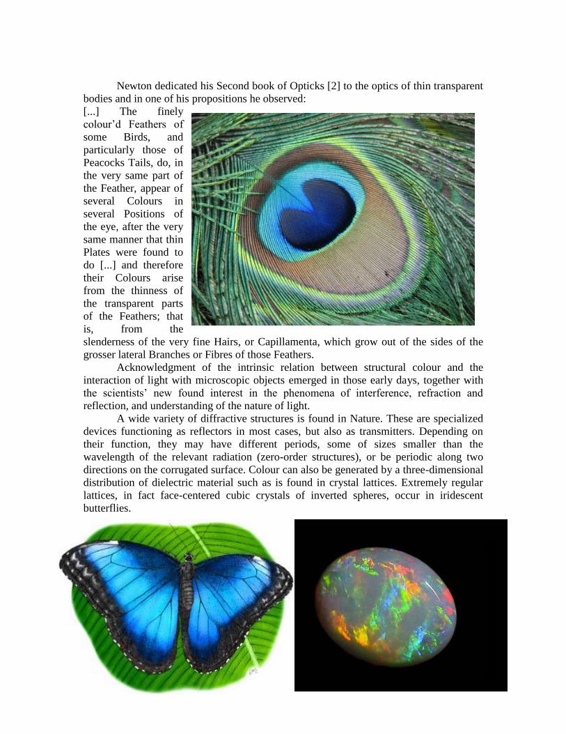
A wide variety of diffractive structures is found in Nature. These are specialized
devices functioning as reflectors in most cases, but also as transmitters. Depending on
their function, they may have different periods, some of sizes smaller than the
wavelength of the relevant radiation (zero-order structures), or be periodic along two
directions on the corrugated surface. Colour can also be generated by a three-dimensional
distribution of dielectric material such as is found in crystal lattices. Extremely regular
lattices, in fact face-centered cubic crystals of inverted spheres, occur in iridescent
butterflies.
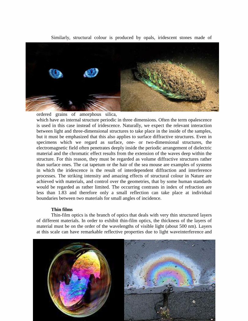
Similarly, structural colour is produced by opals, iridescent stones made of
ordered grains of amorphous silica,
which have an internal structure periodic in three dimensions. Often the term opalescence
is used in this case instead of iridescence. Naturally, we expect the relevant interaction
between light and three-dimensional structures to take place in the inside of the samples,
but it must be emphasized that this also applies to surface diffractive structures. Even in
specimens which we regard as surface, one- or two-dimensional structures, the
electromagnetic field often penetrates deeply inside the periodic arrangement of dielectric
material and the chromatic effect results from the extension of the waves deep within the
structure. For this reason, they must be regarded as volume diffractive structures rather
than surface ones. The cat tapetum or the hair of the sea mouse are examples of systems
in which the iridescence is the result of interdependent diffraction and interference
processes. The striking intensity and amazing effects of structural colour in Nature are
achieved with materials, and control over the geometries, that by some human standards
would be regarded as rather limited. The occurring contrasts in index of refraction are
less than 1.83 and therefore only a small reflection can take place at individual
boundaries between two materials for small angles of incidence.
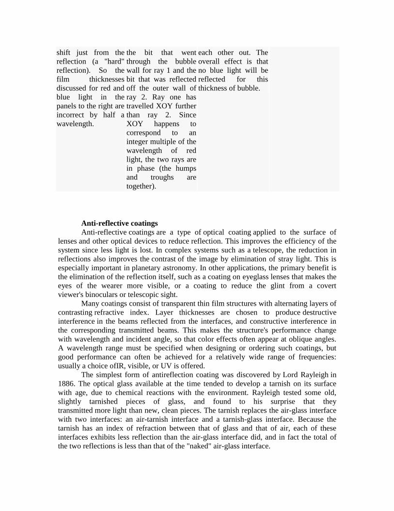
Thin films
Thin-film optics is the branch of optics that deals with very thin structured layers
of different materials. In order to exhibit thin-film optics, the thickness of the layers of
material must be on the order of the wavelengths of visible light (about 500 nm). Layers
at this scale can have remarkable reflective properties due to light waveinterference and

the difference in refractive index between the layers, the air, and the substrate. These
effects alter the way the optic reflects and transmits light. This effect is observable
in soap bubbles and oil slicks.
The iridescent colours of soap bubbles are caused by interfering light waves and
are determined by the thickness of the film. They are not the same as rainbow colours but
are the same as the colours in an oil slick on a wet road.
As light impinges on the film, some of it is reflected off the outer surface while
some of it enters the film and reemerges after being reflected back and forth between the
two surfaces. The total reflection observed is determined by the interference of all these
reflections. Since each traversal of the film incurs a phase shift proportional to the
thickness of the film and inversely proportional to the wavelength, the result of the
interference depends on these two quantities. So at a given thickness, interference is
constructive for some wavelengths and destructive for others, so that white
light impinging on the film is reflected with a hue that changes with thickness.
A change in colour can be observed while the bubble is thinning due to evaporation.
Thicker walls cancel out red (longer) wavelengths, causing a blue-green reflection. Later,
thinner walls will cancel out yellow (leaving blue light), then green (leaving magenta),
then blue (leaving a golden yellow). Finally, when the bubble's wall becomes much
thinner than the wavelength of visible light, all the waves in the visible region cancel
each other out and no reflection is visible at all. When this state is observed, the wall is
thinner than about 25nm, and is probably about to pop. This phenomenon is very useful
when making or manipulating bubbles as it gives an indication of the bubble's fragility.
Interference effects also depend upon the angle at which the light strikes the film, an
effect called iridescence. So, even if the wall of the bubble were of uniform thickness,
one would still see variations of colour due to curvature and/or movement. However, the
thickness of the wall is continuously changing as gravity pulls the liquid downwards, so
bands of colours that move downwards can usually also be observed.
In the diagram above
a ray of light hits the
surface at point X.
Some of the light is
reflected, but some
travels through the
bubble wall and is
reflected at the other
side.
When light directed
from low index
material strikes a
high index material
(air to film), there is a
180 degree phase
In this diagram we
look at two rays of red
light (rays 1 and 2).
Both rays are split as
before and follow two
possible paths, but we
are interested only in
the paths that are
represented by the
solid lines. Consider
the ray emerging at Y.
It consists of two rays
on top of one another:
This is similar to the
previous diagram
except the wavelength
is different. This time
XOY is not an integer
multiple of the
wavelength of blue
light and so ray 1 and
2 arrive at y out of
step. The troughs of
ray 1 line up with the
humps of ray 2 and
the two rays cancel
This computed image
shows the colours
reflected by a thin
film of water
illuminated by
unpolarized white
light. The radius is
proportional to the
thickness of the film,
and the polar angle is
the angle of
incidence.
shift just from the
reflection (a "hard"
reflection). So the
film thicknesses
discussed for red and
blue light in the
panels to the right are
incorrect by half a
wavelength.
the bit that went
through the bubble
wall for ray 1 and the
bit that was reflected
off the outer wall of
ray 2. Ray one has
travelled XOY further
than ray 2. Since
XOY happens to
correspond to an
integer multiple of the
wavelength of red
light, the two rays are
in phase (the humps
and troughs are
together).
each other out. The
overall effect is that
no blue light will be
reflected for this
thickness of bubble.
Anti-reflective coatings
Anti-reflective coatings are a type of optical coating applied to the surface of
lenses and other optical devices to reduce reflection. This improves the efficiency of the
system since less light is lost. In complex systems such as a telescope, the reduction in
reflections also improves the contrast of the image by elimination of stray light. This is
especially important in planetary astronomy. In other applications, the primary benefit is
the elimination of the reflection itself, such as a coating on eyeglass lenses that makes the
eyes of the wearer more visible, or a coating to reduce the glint from a covert
viewer's binoculars or telescopic sight.
Many coatings consist of transparent thin film structures with alternating layers of
contrasting refractive index. Layer thicknesses are chosen to produce destructive
interference in the beams reflected from the interfaces, and constructive interference in
the corresponding transmitted beams. This makes the structure's performance change
with wavelength and incident angle, so that color effects often appear at oblique angles.
A wavelength range must be specified when designing or ordering such coatings, but
good performance can often be achieved for a relatively wide range of frequencies:
usually a choice ofIR, visible, or UV is offered.
The simplest form of antireflection coating was discovered by Lord Rayleigh in
1886. The optical glass available at the time tended to develop a tarnish on its surface
with age, due to chemical reactions with the environment. Rayleigh tested some old,
slightly tarnished pieces of glass, and found to his surprise that they
transmitted more light than new, clean pieces. The tarnish replaces the air-glass interface
with two interfaces: an air-tarnish interface and a tarnish-glass interface. Because the
tarnish has an index of refraction between that of glass and that of air, each of these
interfaces exhibits less reflection than the air-glass interface did, and in fact the total of
the two reflections is less than that of the "naked" air-glass interface.
Interference-based coatings were invented in November 1935 by Alexander
Smakula, who was working for the Carl Zeiss optics company. Anti-reflection coatings
were a German military secret until the early stages of World War II.
There are two separate causes of optical effects due to coatings, often called thick
film and thin film effects. Thick film effects arise because of the difference in the index
of refraction between the layers above and below the coating (or film); in the simplest
case, these three layers are the air, the coating, and the glass. Thick film coatings do not
depend on how thick the coating is, so long as the coating is much thicker than a
wavelength of light. Thin film effects arise when the thickness of the coating is
approximately the same as a quarter or a half a wavelength of light. In this case, the
reflections of a steady source of light can be made to add destructively, and hence reduce
reflections by a separate mechanism. In addition to depending very much on the thickness
of the film, and the wavelength of light, thin film coatings depend on the angle at which
the light strikes the coated surface.
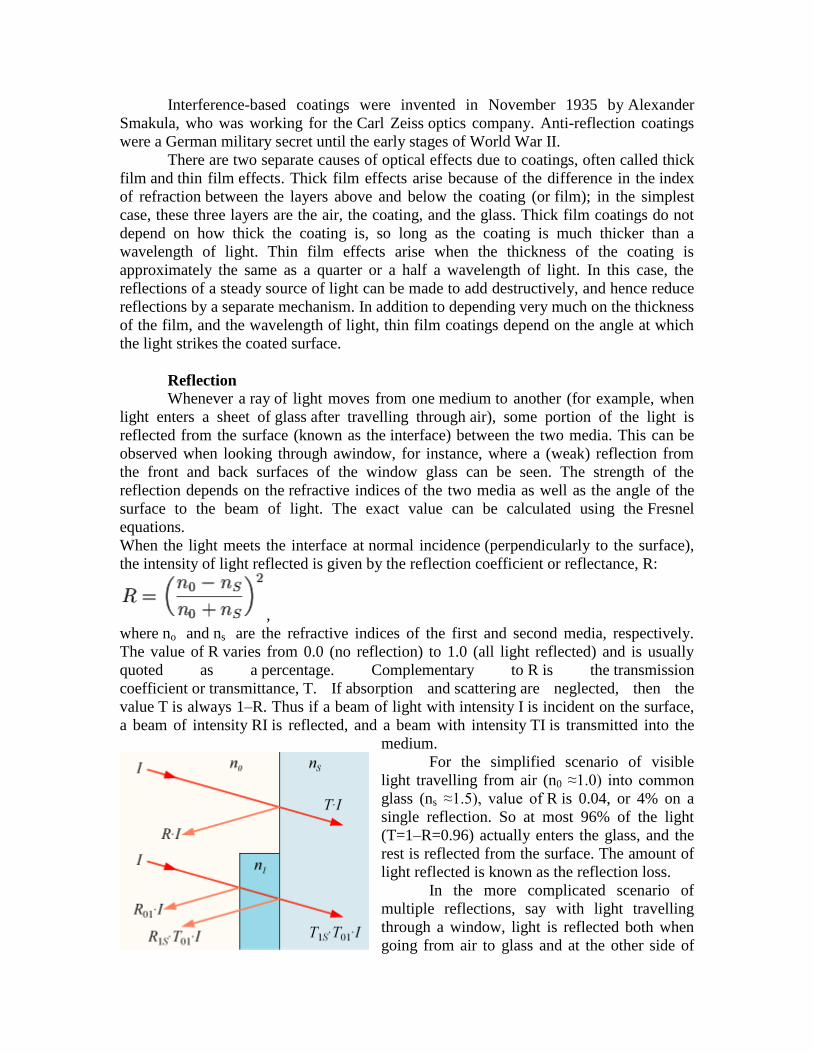
Reflection
Whenever a ray of light moves from one medium to another (for example, when
light enters a sheet of glass after travelling through air), some portion of the light is
reflected from the surface (known as the interface) between the two media. This can be
observed when looking through awindow, for instance, where a (weak) reflection from
the front and back surfaces of the window glass can be seen. The strength of the
reflection depends on the refractive indices of the two media as well as the angle of the
surface to the beam of light. The exact value can be calculated using the Fresnel
equations.
When the light meets the interface at normal incidence (perpendicularly to the surface),
the intensity of light reflected is given by the reflection coefficient or reflectance, R:
,
where no and ns are the refractive indices of the first and second media, respectively.
The value of R varies from 0.0 (no reflection) to 1.0 (all light reflected) and is usually
quoted as a percentage. Complementary to R is the transmission
coefficient or transmittance, T. If absorption and scattering are neglected, then the
value T is always 1–R. Thus if a beam of light with intensity I is incident on the surface,
a beam of intensity RI is reflected, and a beam with intensity TI is transmitted into the
medium.
For the simplified scenario of visible
light travelling from air (n0 ≈1.0) into common
glass (ns ≈1.5), value of R is 0.04, or 4% on a
single reflection. So at most 96% of the light
(T=1–R=0.96) actually enters the glass, and the
rest is reflected from the surface. The amount of
light reflected is known as the reflection loss.
In the more complicated scenario of
multiple reflections, say with light travelling
through a window, light is reflected both when
going from air to glass and at the other side of

the window when going from glass back to air. The size of the loss is the same in both
cases. Light also may bounce from one surface to another multiple times, being partially
reflected and partially transmitted each time it does so. In all, the combined reflection
coefficient is given by 2R/(1+R). For glass in air, this is about 7.7%.)
Rayleigh's film
As observed by Lord Rayleigh, a thin film (such as tarnish) on the surface of glass
can reduce the reflectivity. This effect can be explained by envisioning a thin layer of
material with refractive index n1 between the air (index n0) and the glass (index nS). The
light ray now reflects twice: once from the surface between air and the thin layer, and
once from the layer-to-glass interface.
From the equation above, and the known refractive indices, reflectivities for both
interfaces can be calculated, and denoted R01 and R1S, respectively. The transmission at
each interface is therefore T01 = 1-R01 and T1S = 1-R1S. The total transmitance into the
glass is thusT1ST01. Calculating this value for various values of n1, it can be found that at
one particular value of optimum refractive index of the layer, the transmittance of both
interfaces is equal, and this corresponds to the maximum total transmittance into the
glass.
This optimum value is given by the geometric mean of the two surrounding indices:
.
For the example of glass (nS≈1.5) in air (n0≈1.0), this optimum refractive index
is n1≈1.225. The reflection loss of each interface is approximately 1.0% (with a combined
loss of 2.0%), and an overall transmission T1ST01 of approximately 98%. Therefore an
intermediate coating between the air and glass can halve the reflection loss.
Interference coatings
The use of an intermediate layer to form an antireflection coating can be thought
of as analoguous to the technique of impedance matching of electrical signals. (A similar
method is used in fibre optic research where an index matching oil is sometimes used to
temporarily defeat total internal reflection so that light may be coupled into or out of a
fiber.) Further reduced reflection could in theory be made by extending the process to
several layers of material, gradually blending the refractive index of each layer between
the index of the air and the index of the
substrate.
Practical antireflection coatings,
however, rely on an intermediate layer
not only for its direct reduction of
reflection coefficient, but also use
theinterference effect of a thin layer.
Assume the layer thickness is
controlled precisely, such that it is
exactly one quarter of the light's
wavelength thick (λ/4). The layer is
then called a quarter-wave coating. For
this type of coating the incident beam I,
when reflected from the second
interface, will travel exactly half its

own wavelength further than the beam reflected from the first surface. If the intensities of
the two beams R1 and R2 are exactly equal, they will destructively interfere and cancel
each other since they are exactly out of phase. Therefore, there is no reflection from the
surface, and all the energy of the beam must be in the transmitted ray, T. In the
calculation of the reflection from a stack of layers, the transfer-matrix method can be
used.
Real coatings do not reach perfect performance, though they are capable of
reducing a surface's reflection coefficient to less than 0.1%. Practical details include
correct calculation of the layer thickness; since the wavelength of the light is reduced
inside a medium, this thickness will be λ0 / 4n1, where λ0 is the vacuum wavelength.
Also, the layer will be the ideal thickness for only one distinct wavelength of light. Other
difficulties include finding suitable materials for use on ordinary glass, since few useful
substances have the required refractive index (n≈1.23) which will make both reflected
rays exactly equal in intensity. Magnesium fluoride (MgF2) is often used, since this is
hard-wearing and can be easily applied to substrates using physical vapour deposition,
even though its index is higher than desirable (n=1.38).
Further reduction is possible by using multiple coating layers, designed such that
reflections from the surfaces undergo maximum destructive interference. One way to do
this is to add a second quarter-wave thick higher-index layer between the low-index layer
and the substrate. The reflection from all three interfaces produces destructive
interference and antireflection. Other techniques use varying thicknesses of the coatings.
By using two or more layers, each of a material chosen to give the best possible match of
the desired refractive index and dispersion, broadband antireflection coatings which
cover the visible range (400-700 nm) with maximum reflectivities of less than 0.5% are
commonly achievable.
The exact nature of the coating determines the appearance of the coated optic;
common AR coatings on eyeglasses and photographic lenses often look somewhat bluish
(since they reflect slightly more blue light than other visible wavelengths), though green
and pink-tinged coatings are also used.
If the coated optic is used at non-normal incidence (that is, with light rays not
perpendicular to the surface), the antireflection capabilities are degraded somewhat. This
occurs because the phase accumulated in the layer relative to the phase of the light
immediately reflected decreases as the angle increases from normal. This is
counterintuitive, since the ray experiences a greater total phase shift in the layer than for
normal incidence. This paradox is resolved by noting that the ray will exit the layer
spatially offset from where it entered, and will interfere with reflections from incoming
rays that had to travel further (thus accumulating more phase of their own) to arrive at the
inteface. The net effect is that the relative phase is actually reduced, shifting the coating,
such that the anti-reflection band of the coating tends to move to shorter wavelengths as
the optic is tilted. Non-normal incidence angles also usually cause the reflection to
be polarization dependent.
Photonic crystals
Photonic crystals are composed of periodic dielectric or metallo-
dielectric nanostructures that affect the propagation of electromagnetic waves (EM) in the
same way as the periodic potential in a semiconductor crystal affects the electron motion
by defining allowed and forbidden electronic energy bands. Essentially, photonic crystals
contain regularly repeating internal regions of high and low dielectric constant. Photons
(behaving as waves) propagate through this structure - or not - depending on their
wavelength. Wavelengths of light that are allowed to travel are known as modes, and
groups of allowed modes form bands. Disallowed bands of wavelengths are called
photonic band gaps. This gives rise to distinct optical phenomena such as inhibition
of spontaneous emission, high-reflecting omni-directional mirrors and low-loss-
waveguiding, amongst others. Since the basic physical phenomenon is based
on diffraction, the periodicity of the photonic crystal structure has to be of the same
length-scale as half the wavelength of the EM waves i.e. ~200 nm (blue) to 350 nm (red)
for photonic crystals operating in the visible part of the spectrum - the repeating regions
of high and low dielectric constants have to be of this dimension. This makes the
fabrication of optical photonic crystals cumbersome and complex.
The exploitation of electronic crystals has been one of the most important
revolutions in the history of engineering and has driven the development of modern
physics as we know it. The quantum theories explaining the mechanics of electrons in
different materials have been a source of inspiration for scientists investigating the
interaction between photons and matter. Interest in controlling material radiation has
resulted in the conception of a new class of materials capable of interacting with
electromagnetic waves at a structural level: they are called photonic crystals or photonic
bandgap materials.
History of photonic crystals
Although photonic crystals have been studied in one form or another since 1887,
the term “photonic crystal” was first used over 100 years later, after Eli
Yablonovitch and Sajeev John published two milestone papers on photonic crystals in
1987. Before 1987, one-dimensional photonic crystals in the form of periodic multi-
layers dielectric stacks (such as the Bragg mirror) were studied extensively. Lord
Rayleigh started their study in 1887, by showing that such systems have a one-
dimensional photonic band-gap, a spectral range of large reflectivity, known as a stop-
band. Today, such structures are used in a diverse range of applications; from reflective
coatings to enhancing the efficiency of LEDs to highly reflective mirrors in certain laser
cavities.
Purcell in 1946 indicated that spontaneous emission of radio waves from nuclear
spin levels could be controlled by a dispersion of small metallic particles in a nuclear-
magnetic material, which would create a resonant oscillator. In 1972 Bykov considered
that spontaneous emission of atoms at optical wavelengths could be reduced by placing
them in a periodic lattice of dielectrics with pitches smaller than the radiation
wavelength, thus avoiding decay of excited states through the presence of opaque bands
for the transition radiation and consequent generation of a dynamic state. Bykov also
speculated as to what could happen if two- or three-dimensional periodic optical
structures were used. However, these ideas did not take off until after the publication of
two milestone papers in 1987 by Yablonovitch and John. Both these papers concerned
high dimensional periodic optical structures – photonic crystals. Yablonovitch’s main
motivation was to engineer the photonic density of states, in order to control
the spontaneous emission of materials embedded within the photonic crystal; John’s idea

was to use photonic crystals to affect the localisation and control of light. Both these
works addressed the engineering of a structured material exhibiting ranges of frequencies
at which the propagation of electromagnetic waves is not allowed, so called bandgaps,
and their employment in the emission control of optically active materials.
After 1987, the number of research papers concerning photonic crystals began to
grow exponentially. However, due to the difficulty of actually fabricating these structures
at optical scales, early studies were either theoretical or in the microwave regime, where
photonic crystals can be built on the far more readily accessible centimetre scale. (This
fact is due to a property of the electromagnetic fields known as scale invariance – in
essence, the electromagnetic fields, as the solutions to Maxwell's equations, has no
natural length scale, and so solutions for centimetre scale structure at microwave
frequencies are the same as for nanometre scale structures at optical frequencies.) By
1991, Yablonovitch had demonstrated the first three-dimensional photonic band-gap in
the microwave regime. In 1996, Thomas Krauss made the first demonstration of a two-
dimensional photonic crystal at optical wavelengths. This opened up the way for photonic
crystals to be fabricated in semiconductor materials by borrowing the methods used in the
semiconductor industry. Today, such techniques use photonic crystal slabs, which are two
dimensional photonic crystals “etched” into slabs of semiconductor; total internal
reflection confines light to the slab, and allows photonic crystal effects, such as
engineering the photonic dispersion to be used in the slab. Research is underway around
the world to use photonic crystal slabs in integrated computer chips, in order to improve
the optical processing of communications both on-chip and between chips. Although such
techniques are still to mature into commercial applications, two-dimensional photonic
crystals have found commercial use in the form of photonic crystal fibres (otherwise
known as holey fibres, because of the air holes that run through them). Photonic crystal
fibres were first developed by Philip Russell in 1998, and can be designed to possess
enhanced properties over (normal) optical fibres.
[1] Purcell EM, “Spontaneous emission probabilities at radio frequencies”, Proceedings
of the American Physical Society in Phisical Review, 69, 681 (1946)
[2] Bykov VP, “Spontaneous emission in a periodic structure”, Soviet Physics JETP, 35,
269–273 (1972)
[3] Yablonovich E, “Inhibited spontaneous emission in solid-state physics and
electronics”, Physical Review Letters, 58, 2059–2062 (1987)
[4] John S, “Strong localization of photons in certain disordered dielectric superlattices”,
Physical Review Letters, 58, 2486–2489 (1987)
Modelling photonic crystals and computing photonic band structure
Photonic crystals are essentially bulk materials, because the occurrence of the
bandgap depends, amongst other things, on the modulation of the index of refraction over
a large number of periods. The search for efficient bandgap materials has prompted
scientists to solve Maxwell ’s equations within the periodic arrangement.
The photonic band gap (PBG) is essentially the gap between the air-line and the
dielectric-line in the dispersion relation of the PBG system. To design photonic crystal

systems, it is essential to engineer the location and size of the bandgap; this is done by
computational modeling using any of the following methods:
Transfer-matrix method
Plane wave expansion method.
Finite Difference Time Domain method
Transfer matrix method (TMM)
A multilayer is a stack of homogeneous thin-films with different indices of
refraction and is usually modelled assuming that the arrangement of dielectric materials
be invariant with respect to continuous translation in two orthogonal directions and not in
the third.
The optical theory of thin-films was first presented in 1949 by Schuster [1]. The
following year, Abel`es [2] extended it to multilayers and formalized the computing
technique called the transfer matrix method (TMM). The basic formalism yields the
amplitude of the electromagnetic field of monochromatic waves reflected by and
transmitted through the mentioned structure. The solution is achieved through
propagation of the fields in the homogeneous layers, and the continuity of the tangential
components of the electric and magnetic fields at the interfaces. Although the structure is
onedimensional, propagation for non-normal incidence can be accounted for. The
solutions for plane waves are in fact vectors of the three-dimensional Euclidean space
propagating in a plane. With the exception of approximations in the chosen model, i.e.
simplified dimensionality and initial conditions, or neglect of material parameters, this
analytical method is exact.
The optical properties of stacks of thin layers proposed by Hooke and Newton [3,
4] were confirmed by the TMM calculations, showing that multilayers are characterised
by high reflectivity and transmissivity over large portions of the spectrum. Interest in a
wide variety of important applications of multilayers, including antireflective coatings
(AR), high reflectivity dielectric mirrors and filters, has prompted scientists to use the
TMM to compute new designs. It has been demonstrated how to extend the spectral
region of high reflectance [5], or the range of angles at which the desired effect occurs
[6], and recent studies have presented the extension of the TMM to stacks of anisotropic
materials [7,8], showing how to obtain an omnidirectional reflector with existing
materials. The simple form of the TMM equations applied to a periodically stratified
medium [9] is convenient for systems with a large number of layers, but novel
developments in the study of periodic structures have offered new approaches for the
investigation of periodic multilayers. These techniques involve decomposition of the field
into periodic modes [10], and assume infinitely extended modulations of the index. These
techniques therefore cannot model effects related to the finiteness of a multilayer or the
interaction of light at its boundary with the incident medium, but they have proven
powerful tools to investigate an important property of dielectric stacks: the photonic
bandgap [11].

Pendry et al. [12] suggested an approximative finite-element method (FEM) to
solve Maxwell ’s equations over a discrete mesh of points in a simple cubic lattice. For a
fixed frequency Pendry et al. propagated fields in one of the orthogonal directions of the
lattice by means of an approximate wave vector and, assuming a periodic distribution,
Pendry et al. applied periodic boundary conditions in the planes normal to the
propagation direction. This resulted in a two-dimensional transfer matrix method (TMM)
for the real space fields, which was successively upgraded to its Fourier-space form, to
work in the resonance domain of frequencies, and was capable of fast and accurate
calculation of the response of complex periodic structures [13,14].
[1] Schuster K, “Anwendung der Vierpoltheorie auf die Probleme der optischen
Reflexionsminderung, Reflexionsverstarkung und der Interferenzfilter”, Annalen der
Physik, 6, 352–356 (1949)
[2] Abel`es F, “Recherches sur la propagation des ondes electromagnetiques sinusoıdales
dans les milieux stratifies. Application aux couches minces”, Annales de Physique, 5,
596–640, 706–782 (1950)
[3] Hooke R, Micrographia, London: The Royal Society (1665), reprinted by Palo Alto:
Octavo (1998), ISBN 1891788027.
[4] Newton I, Opticks, fourth edition, London: William Innys (1730), reprinted by New
York: Dover Publications (1952), ISBN 486602052
[5] Turner AF, Baumeister PW, “Multilayer mirrors with high reflectance over an
extended spectral region”, Applied Optics, 5, 69–76 (1966)
[6] Weber MF, Stover CA, Gilbert LR, Nevitt TJ, Ouderkirk AJ, “Giant birefringent
optics in multilayer polymer mirrors”, Science, 287, 2451– 2456 (2000)
[7] Abdulhalim I, “Omnidirectional reflection from anisotropic periodic dielectric stack”,
Optics Communications, 174, 43–50 (2000)
[8] Cojocaru J, “Forbidden gaps in periodic anisotropic layered media”, Applied Optics,
39, 4641–4648 (2000)
[9] Born M, Wolf E, Priciples of Optics, seventh edition, Cambridge: Cambridge
University Press (1999), ISBN 0521642221
[10] Joannopoulos JD, Meade RD, Winn JN, Photonic Crystals, Princeton: Princeton
University Press (1995), ISBN 0691037442
[11] Fink Y, Winn JN, Fan S, Chen C, Michel J, Joannopoulos JD, Thomas EL, “A
dielectric omnidirectional reflector”, Science, 282, 1679–1682 (1998)
[12] Pendry JB, MacKinnon A, “Calculation of photon dispersion relations”, Physical
Review Letters, 69, 2772–2775 (1992) 194
[13] Pendry JB, “Photonic band structures”, Journal of Modern Optics, 41, 209–229
(1994)
[14] Guida G, Stavrinou PN, Parry G, Pendry JB, “Time-reversal symmetry,
microcavities and photonic crystals”, Journal of Modern Optics, 48, 581–595 (2001)
Plane wave method (PWM)
Gratings have been the object of intense study ever since 18th century scientists
comprehended their usefulness in optics. A grating is traditionally an evenly spaced array
of straight grooves on a planar surface, and is modelled as a distribution of material
(dielectric or not) periodic in one direction and invariant with respect to continuous

translation in the other. However, surface distributions periodic in two directions, found
in Nature and which have also been fabricated, are often equally referred to as gratings.
With gratings, the ratio between the wavelength of the interacting light and the size of
their features is a crucial quantity when modelling them. Depending on the wavelength-
to-pitch and wavelength-to-depth ratios of an array of diffractive elements, differing
computing techniques must be adopted. Gratings with large pitches compared to the
operating wavelength are called coarse, while those with a small depth-to-period ratio are
termed shallow.
The scalar theory for diffraction gratings developed by Kirchhoff in the 19th
century [1] has been a very successful one, but it is accurate only for coarse and shallow
gratings. Modelling of gratings with large wavelength-to-pitch ratios requires a rigorous
solution of Maxwell ’s equations. Assuming discrete translational symmetry and
therefore infinite extension of the modulation, the fields decompose into periodic modes.
A solution is obtained by expansion in the zone of the periodic distribution of index of
refraction with periodic functions, and by energy conservation at its boundaries. The
major difficulty with this method is to find a solution formulation for the scattering
problem of a single diffraction element, which is also laterally periodic.
A method to rigorously obtain the diffraction of plane gratings with rectangular
diffraction elements, the rigorous modal method (RMM), was proposed by Knop [2].
With the RMM, an incoming plane wave is projected onto the Fourier basis functions and
substituted into the Helmholtz equation. The incident field is separated into its
components parallel and perpendicular to the plane of incidence and the problems for
transverse electric (TE) and transverse magnetic (TM) polarisations are solved separately.
With the simultaneous Fourier expansion of the dielectric function in the periodic
medium zone, this yields a standard eigenvalue problem. The direction of propagation of
the modes is obtained from the solution of the eigenvalue problem, the size of which
depends on the order of truncation in the expansions, and the modes are successively
propagated in the periodic medium. The tangential components of the fields for all the
expansion orders are then matched at the boundaries between media (usually the isotropic
incidence and substrate media, and layers of periodic arrangement of dielectric) and
finally the amplitudes and phases of the diffracted waves are extracted. Although this
rigorous technique is in principle applicable to diffractive elements of arbitrary shape, in
practice the eigenvalue problem can only be obtained for lamellar gratings because of the
limitation in finding a suitable solution formulation. For both methods, numerical
instabilities in the solution of the TM problem result in poor convergence and therefore
poor accuracy. The instabilities are related to the Fourier expansion of the dielectric
constant and are referred to as Gibbs phenomena.
Ho et al. [3] were the first to correctly predict the existence of a complete bandgap
in a specific photonic crystal structure, i.e. a range of frequencies at which no
propagation of waves is possible in any direction in the crystal. By means of a plane
wave expansion method (PWM) they calculated the size of the bandgap for a diamond
lattice of spheres, and established its dependence upon the dielectric contrast and filling
fraction parameters. Ho et al. showed that a face-centered cubic lattice of spheres cannot
have a complete bandgap.
The PWM is a three-dimensional version of the Fourier expansion technique
mentioned when we discussed the rigorous modal method. The same difficulties have to

be addressed here as in the one-dimensional case of lamellar gratings, namely a solution
for the single scatterer must be found which is periodic along the crystal axes, and
numerical instabilities are encountered due to Gibb’s phenomena. Analytical solutions
are therefore only found for systems composed of spheres in space, and cylindrical or
rectangular rods in a plane of the crystal. Convergence issues related to Gibb’s
phenomena are addressed using different expansion bases. Whichever the method of
expansion used, the total number of terms is determined by the order of the truncation to
the power of the number of dimensions in the problem.
The requirements for computation in terms of storage memory and speed of
processing grow exponentially with increasing dimensionality of the problem to solve.
Arbitrarily shaped “atoms” require numerical integration over the unit cell of the crystal,
which is again very demanding computationally and even places many low dimensional
problems beyond reach. Nevertheless, advances in this field have produced numerical
methods which reduce the computational obstacles. By means of iterative optimization of
an approximative initial solution, through a parallel computing approach via block matrix
diagonalisation, or implementing ingenuous numerical measures, such as smoothing the
dielectric function[4], many previously unattainable numerical calculations have been
successfully solved.
The PWM was adapted by Sakoda [5] to compute the diffraction of two-
dimensional periodic bandgap materials with a finite thickness. Using a plane wave
expansion in the direction of periodicity of the dielectric function and an arbitrary Fourier
expansion normally to that same plane, diffracted fields were successively matched to the
field expansions within the periodic medium. Predictions of the diffraction of triangular
and square lattices of air rods in planar waveguides were obtained in this way with good
accuracy [6,7].
[1] Born M, Wolf E, Priciples of Optics, seventh edition, Cambridge: Cambridge
University Press (1999), ISBN 0521642221
[2] Knop K, “Rigorous diffraction theory for transmission phase gratings with deep
rectangular grooves”, Journal of the Optical Society of America, 68, 1206–1210 (1978)
[3] Ho KM, Chan CT, Soukoulis CM, “Existence of a Photonic Gap in Periodic
Dielectric Structures”, Physical Review Letters, 65, 3152–3155 (1990)
[4] Johnson SG, Joannoupoulos JD, “Block-iterative frequency-domain methods for
Maxwell’s equations in a planewave basis”, Optics Express, 8, 173–190 (2001)
[5] Sakoda K, “Transmittance and Bragg reflectivity of two-dimensional photonic
lattices”, Physical Review B, 52, 8992–9002 (1995)
[6] Labilloy D, Benisty H, Weisbuch C, Krauss TF, De La Rue RM, Bardinal V, Houdre
R, Oesterle U, Cassagne D, Jouanin C, “Quantitative measurement of transmission,
reflection, and diffraction of twodimensional photonic band gap strucutres at near-
infrared wavelengths”, Physical Review Letters, 79, 4147–4150 (1997)
[7] Benisty H, Weisbuch C, Labilloy D, Rattier M, Smith CJM, Krauss TF, De La Rue
RM, Houdre R, Oesterle U, Jouanin C, Cassagne D, “Optical and confinement properties
of two-dimensional photonic crystals ”, Journal of Lightwave Technology, 17, 2063–
2076 (1999)
Finite-difference time-domain (FDTD)

Another method to solve Maxwell ’s equations on a discrete lattice of points in
space is the finite-difference time-domain (FDTD) method. This method has a long
history and has been used in a variety of applications which are reviewed in the book
edited by Taflove [1]. In 1995 Chan et al. [2] were the first to apply this method to
compute the band structure of photonic crystals and to prove its reliability in treating
periodic structures of high complexity. The FDTD calculations are particularly useful for
complicated structures because the memory and processing time requirements scale
linearly with the number of grid-points included in the computation, allowing resolution
of minute and intricate structures. With the FDTD method an initial field is propagated
applying the governing equations in a first-order differential form, both in space and
time, at all points in the grid in a succession of time steps. Different types of boundary
conditions can be applied including periodic ones, particularly useful for this type of
system. The fields at selected points on the grid are finally Fourier-transformed from the
time to the frequency domain such that observations on spectral content can be made.
Ward and Pendry [3] extended the FDTD method to nonorthogonal meshes, proved that
the approximation of the equations conserves energy just as the original ones, and
showed how to obtain the Green’s function of a system. The FDTD method allows
solution of the governing equations inside a periodic structure, but also outside at the
same time, offering a tool to study the coupling of waves between different media or
devices, and the diffraction or scattering of light.
[1] Taflove A, Advances in Computational Electrodynamics: the Finitedifference Time-
domain Method, Norwood MA: Artech House (1998), ISBN 0890068348
[2] Chan CT, Yu QL, Ho KM, “Order-N spectral method for electromagnetic waves”,
Physical Review B, 51, 16635–16642 (1995)
[3] Ward AJ, Pendry JB, “Calculating photonic Green’s functions using a nonorthogonal
finite-difference time-domain method”, Physical Review B, 58, 7252–7259 (1998)
More on Finite-difference time-domain method
Finite-difference time-domain (FDTD) is a popular computational
electrodynamics modeling technique. It is considered easy to understand and easy to
implement in software. Since it is a time-domain method, solutions can cover a wide
frequency range with a single simulation run.
The FDTD method belongs in the general class of grid-based differential time-
domain numerical modeling methods. The time-dependentMaxwell's equations (in partial
differential form) are discretized using central-difference approximations to the space and
time partial derivatives. The resulting finite-difference equations are solved in either
software or hardware in a leapfrog manner: the electric field vector components in a
volume of space are solved at a given instant in time; then the magnetic field vector
components in the same spatial volume are solved at the next instant in time; and the
process is repeated over and over again until the desired transient or steady-state
electromagnetic field behavior is fully evolved.
The basic FDTD space grid and time-stepping algorithm trace back to a seminal
1966 paper by Kane Yee in IEEE Transactions on Antennas and Propagation (Yee 1966).
The descriptor "Finite-difference time-domain" and its corresponding "FDTD" acronym
were originated by Allen Taflove in a 1980 paper in IEEE Transactions on
Electromagnetic Compatibility (Taflove 1980). See "References" for these and other
important journal papers in the development of FDTD techniques, as well as relevant
textbooks and research monographs.
Since about 1990, FDTD techniques have emerged as primary means to
computationally model many scientific and engineering problems dealing
with electromagnetic wave interactions with material structures. As summarized in
Taflove & Hagness (2005), current FDTD modeling applications range from near-DC
(ultralow-frequency geophysics involving the entire Earth-ionosphere waveguide)
through microwaves (radar signature technology, antennas, wireless communications
devices, digital interconnects, biomedical imaging/treatment) to visible light (photonic
crystals, nanoplasmonics, solitons, and biophotonics). In 2006, an estimated 2,000
FDTD-related publications appeared in the science and engineering literature (see
"Growth of FDTD publications"). At present, there are at least 27 commercial/proprietary
FDTD software vendors; 8 free-software/open-source-software FDTD projects; and 2
freeware/closed-source FDTD projects, some not for commercial use.
Workings of the FDTD method
When Maxwell's differential equations are examined, it can be seen that the
change in the E-field in time (the time derivative) is dependent on the change in the H-
field across space (the curl). This results in the basic FDTD time-stepping relation that, at
any point in space, the updated value of the E-field in time is dependent on the stored
value of the E-field and the numerical curl of the local distribution of the H-field in space
(Yee 1966).
The H-field is time-stepped in a similar manner. At any point in space, the
updated value of the H-field in time is dependent on the stored value of the H-field and
the numerical curl of the local distribution of the E-field in space. Iterating the E-field
and H-field updates results in a marching-in-time process wherein sampled-data analogs
of the continuous electromagnetic waves under consideration propagate in a numerical
grid stored in the computer memory.
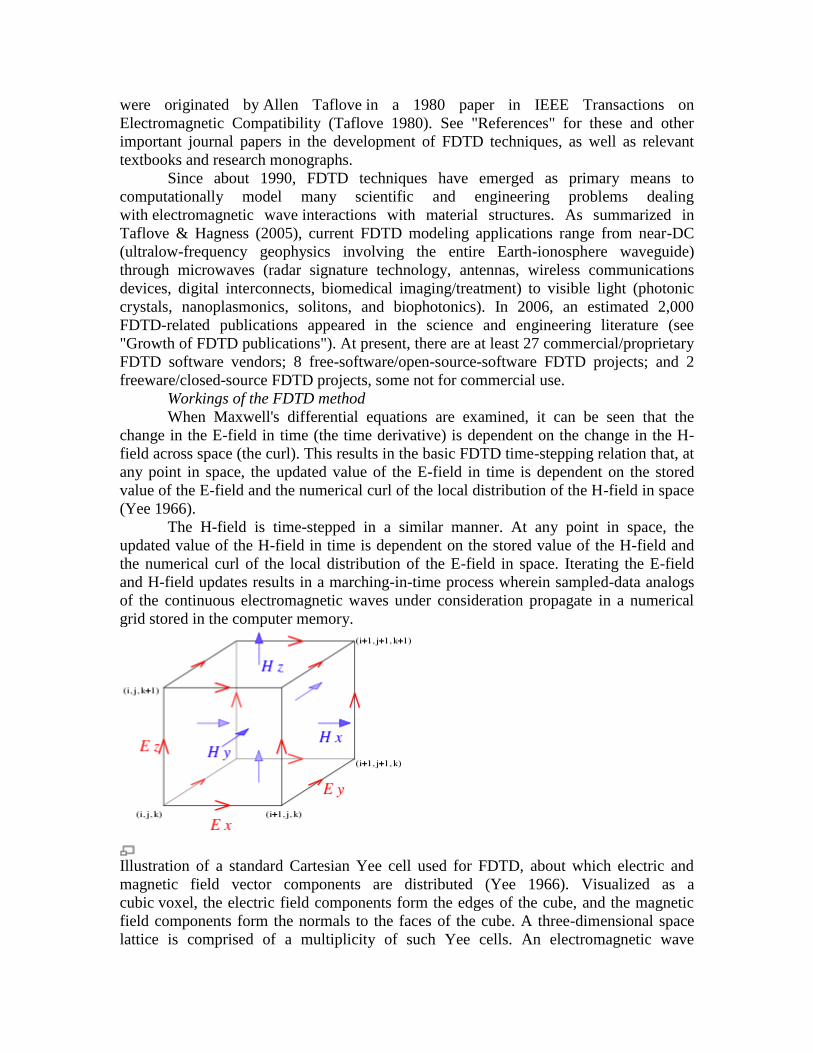
Illustration of a standard Cartesian Yee cell used for FDTD, about which electric and
magnetic field vector components are distributed (Yee 1966). Visualized as a
cubic voxel, the electric field components form the edges of the cube, and the magnetic
field components form the normals to the faces of the cube. A three-dimensional space
lattice is comprised of a multiplicity of such Yee cells. An electromagnetic wave

interaction structure is mapped into the space lattice by assigning appropriate values of
permittivity to each electric field component, and permeability to each magnetic field
component.
This description holds true for 1-D, 2-D, and 3-D FDTD techniques. When
multiple dimensions are considered, calculating the numerical curl can become
complicated. Kane Yee's seminal 1966 paper in IEEE Transactions on Antennas and
Propagation proposed spatially staggering the vector components of the E-field and H-
field about rectangular unit cells of a Cartesian computational grid so that each E-field
vector component is located midway between a pair of H-field vector components, and
conversely. This scheme, now known as a Yee lattice, has proven to be very robust, and
remains at the core of many current FDTD software constructs (Yee 1966).
Furthermore, Yee proposed a leapfrog scheme for marching in time wherein the
E-field and H-field updates are staggered so that E-field updates are conducted midway
during each time-step between successive H-field updates, and conversely (Yee 1966).
On the plus side, this explicit time-stepping scheme avoids the need to solve
simultaneous equations, and furthermore yields dissipation-free numerical wave
propagation. On the minus side, this scheme mandates an upper bound on the time-step to
ensure numerical stability (Taflove & Brodwin 1975). As a result, certain classes of
simulations can require many thousands of time-steps for completion.
Using the FDTD method
In order to use FDTD a computational domain must be established. The
computational domain is simply the physical region over which the simulation will be
performed. The E and H fields are determined at every point in space within that
computational domain. The material of each cell within the computational domain must
be specified. Typically, the material is either free-space (air), metal, ordielectric. Any
material can be used as long as the permeability, permittivity, and conductivity are
specified.
Once the computational domain and the grid materials are established, a source is
specified. The source can be an impinging plane wave, a current on a wire, or an applied
electric field, depending on the application.
Since the E and H fields are determined directly, the output of the simulation is
usually the E or H field at a point or a series of points within the computational domain.
The simulation evolves the E and H fields forward in time. Processing may be done on
the E and H fields returned by the simulation. Data processing may also occur while the
simulation is ongoing. While the FDTD technique computes electromagnetic fields
within a compact spatial region, scattered and/or radiated far fields can be obtained via
near-to-far-field transformations, as reported originally by Umashankar and Taflove
(1982).
Strengths of FDTD modeling
Every modeling technique has strengths and weaknesses, and the FDTD method
is no different. FDTD is a versatile modeling technique used to solve Maxwell's
equations. It is intuitive, so users can easily understand how to use it and know what to
expect from a given model.
FDTD is a time-domain technique, and when a broadband pulse (such as a
Gaussian pulse) is used as the source, then the response of the system over a wide range
of frequencies can be obtained with a single simulation. This is useful in applications

where resonant frequencies are not exactly known, or anytime that a broadband result is
desired.
Since FDTD calculates the E and H fields everywhere in the computational
domain as they evolve in time, it lends itself to providing animated displays of the
electromagnetic field movement through the model. This type of display is useful in
understanding what is going on in the model, and to help ensure that the model is
working correctly.
The FDTD technique allows the user to specify the material at all points within
the computational domain. A wide variety of linear and nonlinear dielectric and magnetic
materials can be naturally and easily modeled.
FDTD allows the effects of apertures to be determined directly. Shielding effects
can be found, and the fields both inside and outside a structure can be found directly or
indirectly.
FDTD uses the E and H fields directly. Since most EMI/EMC modeling
applications are interested in the E and H fields, it is convenient that no conversions must
be made after the simulation has run to get these values.
Weaknesses of FDTD modeling
Since FDTD requires that the entire computational domain be gridded, and the
grid spatial discretization must be sufficiently fine to resolve both the smallest
electromagnetic wavelength and the smallest geometrical feature in the model, very large
computational domains can be developed, which results in very long solution times.
Models with long, thin features, (like wires) are difficult to model in FDTD because of
the excessively large computational domain required.
FDTD finds the E/H fields directly everywhere in the computational domain. If
the field values at some distance are desired, it is likely that this distance will force the
computational domain to be excessively large. Far-field extensions are available for
FDTD, but require some amount of postprocessing (Taflove & Hagness 2005).
Since FDTD simulations calculate the E and H fields at all points within the
computational domain, the computational domain must be finite to permit its residence in
the computer memory. In many cases this is achieved by inserting artificial boundaries
into the simulation space. Care must be taken to minimize errors introduced by such
boundaries. There are a number of available highly effective absorbing boundary
conditions (ABCs) to simulate an infinite unbounded computational domain (Taflove &
Hagness 2005). Most modern FDTD implementations instead use a special absorbing
"material", called a perfectly matched layer (PML) to implement absorbing boundaries
(Berenger 1994, Gedney 1996).
Because FDTD is solved by propagating the fields forward in the time domain,
the electromagnetic time response of the medium must be modeled explicitly. For an
arbitrary response, this involves a computationally expensive time convolution, although
in most cases the time response of the medium (or Dispersion (optics)) can be adequately
and simply modeled using either the recursive convolution (RC) technique, the auxiliary
differential equation (ADE) technique, or the Z-transform technique. An alternative way
of solving Maxwell's equations that can treat arbitrary dispersion easily is the
Pseudospectral Spatial-Domain method (PSSD), which instead propagates the fields
forward in space.

Transfer-matrix method
Fresnel equations
The Fresnel equations, deduced by Augustin-Jean Fresnel, describe the behaviour
of light when moving between media of differing refractive indices.
When light moves from a medium of a given refractive index n1 into a second medium
with refractive index n2 , both reflection and refraction of the light may occur.
In the diagram on the right, an incident
light ray PO strikes at point O the interface
between two media of refractive
indexes n1 and n2. Part of the ray is
reflected as rayOQ and part refracted as
ray OS. The angles that the incident,
reflected and refracted rays make to
the normal of the interface are given as θi,
θr and θt, respectively. The relationship
between these angles is given by the law
of reflection and Snell's law.
The fraction of the
incident power that is reflected from the interface is given by the reflection coefficient R,
and the fraction that is refracted is given by the transmission coefficient T. The media are
assumed to be non-magnetic.
The calculations of R and T depend on polarisation of the incident ray. If the light
is polarised with the electric field of the light perpendicular to the plane of the diagram
above (s-polarised), the reflection coefficient is given by:
where θt can be derived from θi by Snell's law and is simplified using trigonometric
identities.
If the incident light is polarised in the plane of the diagram (p-polarised), the R is given
by:
The transmission coefficient in each case is given by Ts = 1 − Rs and Tp = 1 − Rp.
If the incident light is unpolarised (containing an equal mix of s- and p-polarisations), the
reflection coefficient is R = (Rs + Rp)/2.
Equations for coefficients corresponding to ratios of the electric field amplitudes of the
waves can also be derived, and these are also called "Fresnel equations".

At one particular angle for a given n1 and n2 , the value of Rp goes to zero and a p-
polarised incident ray is purely refracted. This angle is known as Brewster's angle, and is
around 56° for a glass medium in air or vacuum. Note that this statement is only true
when the refractive indexes of both materials are real numbers, as is the case for materials
like air and glass.
For materials that absorb light, like metals andsemiconductors, n is complex,
and Rp does not generally go to zero.
When moving from a denser medium into a less dense one (i.e., n1 > n2 ), above
an incidence angle known as the critical angle, all light is reflected and Rs = Rp = 1. This
phenomenon is known as total internal reflection. The critical angle is approximately 41°
for glass in air.
When the light is at near-normal incidence to the interface (θi ≈ θt ≈ 0), the
reflection and transmission coefficient are given by:
For common glass, the reflection coefficient is about 4%. Note that reflection by a
window is from the front side as well as the back side, and that some of the light bounces
back and forth a number of times between the two sides. The combined reflection
coefficient for this case is 2R/(1 + R), when interference can be neglected. (See below.)
It should be noted that the discussion given here assumes that the permeability μ is equal
to the vacuum permeability μo in both media. This is approximately true for
most dielectric materials, but not for some other types of material. The completely
general Fresnel equations are more complicated.

Transfer-matrix method
The transfer-matrix method is a method used
in optics and acoustics to analyze the propagation of
electromagnetic or acoustic waves through
a stratified (layered) medium. This is for example
relevant for the design of anti-reflective
coatings and dielectric mirrors.
The reflection of light from a single interface
between two media is described by the Fresnel equations.
However, when there are multiple interfaces, such as in
the figure, the reflections themselves are also partially reflected. Depending on the exact
path length, these reflections can interfere destructively or constructively. The overall
reflection of a layer structure is the sum of an infinite number of reflections, which is
cumbersome to calculate.
The transfer-matrix method is based on the fact that, according to Maxwell's
equations, there are simple continuity conditions for the electric field across boundaries
from one medium to the next. If the field is known at the beginning of a layer, the field at
the end of the layer can be derived from a simple matrixoperation. A stack of layers can
then be represented as a system matrix, which is the product of the individual layer
matrices. The final step of the method involves converting the system matrix back into
reflection and transmission coefficients.
Below is described how the transfer matrix is applied to electromagnetic waves
(for example light) of a given frequency propagating through a stack of layers at normal
incidence. It can be generalized to deal with incidence at an angle, absorbing media, and
media with magnetic properties. We assume that the stack layers are normal to the axis
and that the field within one layer can be represented as the superposition of a left- and
right-traveling wave with wave number ,
.
Because it follows from Maxwell's equation that and must be
continuous across a boundary, it is convenient to represent the field as the
vector , where
.
Since there are two equations relating and to and , these two representations
are equivalent. In the new representation, propagation over a distance into the
positive direction is described by the matrix
and

Such a matrix can represent propagation through a layer if is the wave number in the
medium and the thickness of the layer: For a system with layers, each layer has a
transfer matrix , where increases towards higher values. The system transfer
matrix is then
Typically, one would like to know the reflectance and transmittance of the layer
structure. If the layer stack starts at , then for negative , the field is described as
,
where is the amplitude of the incoming wave, the wave number in the left
medium, and is the amplitude (not intensity!) reflectance coefficient of the layer
structure. On the other side of the layer structure, the field consists of a right-propagating
transmitted field
,
where is the amplitude transmittance and is the wave number in the rightmost
medium. If and , then we can solve
in terms of the matrix elements of the system matrix and obtain
,
and
.
The intensity transmittance and reflectance, which are often of more practical use,
are and , respectively.
Fabry-Pérot interferometer
As an illustration, consider a single layer of glass with a refractive index n and
thickness d suspended in air at a wave number k (in air). In glass, the wave number
is . The transfer matrix is
.
The amplitude reflection coefficient can be simplified to
.
This configuration effectively describes a Fabry-Pérot interferometer or etalon:
for , the reflection vanishes.

The varying transmission function of an etalon is caused by interference between
the multiple reflections of light between the two reflecting surfaces. Constructive
interference occurs if the transmitted beams are in phase, and this corresponds to a high-
transmission peak of the etalon. If the transmitted beams are out-of-phase, destructive
interference occurs and this corresponds to a transmission minimum. Whether the
multiply-reflected beams are in-phase or not depends on the wavelength (λ) of the light
(in vacuum), the angle the light travels through the etalon (θ), the thickness of the etalon
(l) and the refractive index of the material between the reflecting surfaces (n).
The phase difference between each succeeding reflection is given by δ:
If both surfaces have a reflectance R, the transmittance function of the etalon is given by:
where is the coefficient of finesse.
The transmission of an
etalon as a function of
wavelength. A high-finesse
etalon (red line) shows sharper
peaks and lower transmission
minima than a low-finesse etalon
(blue).
Maximum transmission
(Te = 1) occurs when the optical
path length difference (2nl cos θ)
between each transmitted beam
is an integer multiple of the
wavelength. In the absence of
absorption, the reflectance of the etalon Reis the complement of the transmittance, such
that Te + Re = 1. The maximum reflectivity is given by:
and this occurs when the path-length difference is equal to half an odd multiple of the
wavelength.
The wavelength separation between adjacent transmission peaks is called the free
spectral range (FSR) of the etalon, Δλ, and is given by:
where λ0 is the central wavelength of the nearest transmission peak. The FSR is related to
the full-width half-maximum, δλ, of any one transmission band by a quantity known as
the finesse:
.
This is commonly approximated (for R > 0.5) by
Etalons with high finesse show sharper transmission peaks with lower minimum
transmission coefficients.
A Fabry-Pérot interferometer differs from a Fabry-Pérot etalon in the fact that the
distance l between the plates can be tuned in order to change the wavelengths at which
transmission peaks occur in the interferometer. Due to the angle dependence of the
transmission, the peaks can also be shifted by rotating the etalon with respect to the
beam.
Fabry-Pérot interferometers or etalons are used
in optical modems,spectroscopy, lasers, and astronomy.
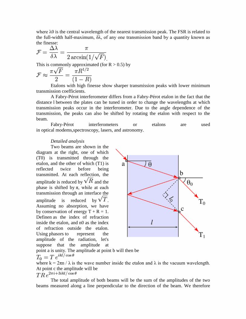
Detailed analysis
Two beams are shown in the
diagram at the right, one of which
(T0) is transmitted through the
etalon, and the other of which (T1) is
reflected twice before being
transmitted. At each reflection, the
amplitude is reduced by and the
phase is shifted by π, while at each
transmission through an interface the
amplitude is reduced by .
Assuming no absorption, we have
by conservation of energy T + R = 1.
Definen as the index of refraction
inside the etalon, and n0 as the index
of refraction outside the etalon.
Using phasors to represent the
amplitude of the radiation, let's
suppose that the amplitude at
point a is unity. The amplitude at point b will then be
where k = 2πn / λ is the wave number inside the etalon and λ is the vacuum wavelength.
At point c the amplitude will be
The total amplitude of both beams will be the sum of the amplitudes of the two
beams measured along a line perpendicular to the direction of the beam. We therefore

add the amplitude at point b to an amplitude T1 equal in magnitude to the amplitude at
point c, but which has been retarded in phase by an amount k0l0 where k0 = 2πn0 / λ is
the wave number outside of the etalon. Thus:
where l0 is seen to be:
Neglecting the 2π phase change due to the two reflections, we have for the phase
difference between the two beams
The relationship between θ and θ0 is given by Snell's law:
So that the phase difference may be written
To within a constant multiplicative phase factor, the amplitude of the m-th transmitted
beam can be written as
The total transmitted beam is the sum of all individual beams
The series is a geometric series whose sum can be expressed analytically. The amplitude
can be rewritten as
The intensity of the beam will be just and, since the incident beam was assumed
to have an intensity of unity, this will also give the transmission function:
Transfer matrix

Scattering matrix
Airy's formulas
For two systems, the multiplication of two transfer-matrices M13=M12M23 gives:
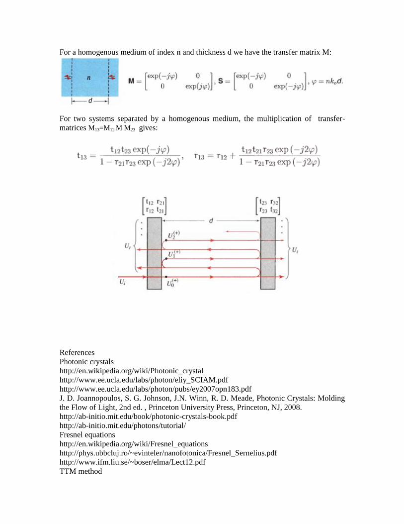
For a homogenous medium of index n and thickness d we have the transfer matrix M:
For two systems separated by a homogenous medium, the multiplication of transfer-
matrices M13=M12 M M23 gives:
References
Photonic crystals
http://en.wikipedia.org/wiki/Photonic_crystal
http://www.ee.ucla.edu/labs/photon/eliy_SCIAM.pdf
http://www.ee.ucla.edu/labs/photon/pubs/ey2007opn183.pdf
J. D. Joannopoulos, S. G. Johnson, J.N. Winn, R. D. Meade, Photonic Crystals: Molding
the Flow of Light, 2nd ed. , Princeton University Press, Princeton, NJ, 2008.
http://ab-initio.mit.edu/book/photonic-crystals-book.pdf
http://ab-initio.mit.edu/photons/tutorial/
Fresnel equations
http://en.wikipedia.org/wiki/Fresnel_equations
http://phys.ubbcluj.ro/~evinteler/nanofotonica/Fresnel_Sernelius.pdf
http://www.ifm.liu.se/~boser/elma/Lect12.pdf
TTM method

Saleh B.E.A.,Teich M.C.Fundamentals of Photonics, Wiley, 2ed, 2007, chap.7
http://en.wikipedia.org/wiki/Transfer-matrix_method_(optics)
http://phys.ubbcluj.ro/~evinteler/nanofotonica/TTM_Sernelius.pdf
http://www.ifm.liu.se/~boser/elma/Lect13.pdf
Program Translight and manual written by A.Reynolds
http://phys.ubbcluj.ro/~evinteler/nanofotonica/translight_manual_Reynolds.pdf
http://phys.ubbcluj.ro/~evinteler/nanofotonica/programs
Based on Saleh B.E.A.,Teich M.C.Fundamentals of Photonics, Wiley, 2ed, 2007,chap.7
Evaluation tests
1. Homogenuos medium
For a homogenous medium of index n and thickness d show that the transfer matrix M is:
Hint: Use the definition of scattering matrix S and determine the reflection and
transmission coefficients with Fresnel equations.
2. Single Dielectric Boundary
Show that at the boundary between two media of refractive indexes n1 and n2 the
scattering and transfer matrix is:
3. Propagation Followed by a Boundary
Show that for a homogeneous medium followed by the boundary between two media of
refractive indexes n1 and n2 the scattering and transfer matrix is:

4. Propagation Followed by Transmission Through a Slab.
Show that for a two homogeneous media with refractive indexes n1 and n2 and
thicknesses d1 and d2 the transfer matrix is:
where:
and transmission coeficient is:
Hint: Use the relation between the scattering and transfer matrices.
5. Single Dielectric Boundary. Oblique TE and TM waves
Show that a wave transmitted through a planar boundary between media of refractive
indexes n1 and n2 at angles θ1 and θ2, satisfying Snell's law (n1 sin θ1 =n2 sin θ2), is
described by a scattering and transfer matrix determined from the Fresnel equations:
6. Off-axis Propagation Followed by Transmission Through a Slab.
Show that for a slab with thickness d and refractive indexes n2 between two
homogeneous media with refractive index n1, the transfer matrix is:
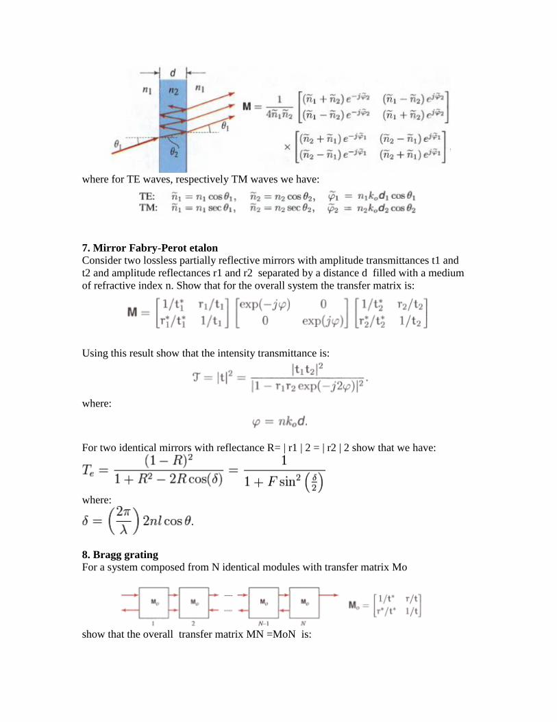
where for TE waves, respectively TM waves we have:
7. Mirror Fabry-Perot etalon
Consider two lossless partially reflective mirrors with amplitude transmittances t1 and
t2 and amplitude reflectances r1 and r2 separated by a distance d filled with a medium
of refractive index n. Show that for the overall system the transfer matrix is:
Using this result show that the intensity transmittance is:
where:
For two identical mirrors with reflectance R= | r1 | 2 = | r2 | 2 show that we have:
where:
8. Bragg grating
For a system composed from N identical modules with transfer matrix Mo
show that the overall transfer matrix MN =MoN is:
Hint: Use the unimodularity of matrix Mo (det Mo=1).
Using the fact that:
show that intensity transmittance and reflectance is:
In the limit for the reflectance of a single module show that:
9. Periodic medium
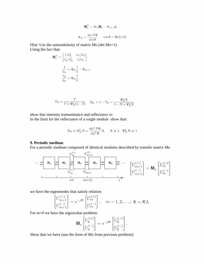
For a periodic medium composed of identical modules described by transfer matrix Mo
we have the eigenmodes that satisfy relation:
For m=0 we have the eigenvalue problem:
Show that we have (use the form of Mo from previous problem):

Hint: Use relations:
10. 1D photonic crystal: Alternating dielectric layers
Show that for the system in the figure we have the following dispersion relation:
where:
Plot dispersion relation in coordinates K,ω and show that we have photonic bandgaps
around frequency values m*ωB :

Hint: Use the relation obtained in the previous problem:
and replace transmission t obtained from problem 4 (Propagation Followed by
Transmission Through a Slab) by phases: