Embed Size (px)
Citation preview
OpenStax-CNX module: m25712 1
Molecular Beam Epitaxy*
Andrew R. Barron
This work is produced by OpenStax-CNX and licensed under the
Creative Commons Attribution License 3.0�
note: This module was developed as part of the Rice University course CHEM-496: Chemistry of
Electronic Materials. This module was prepared with the assistance of Sarah Westcott.
1 Introduction
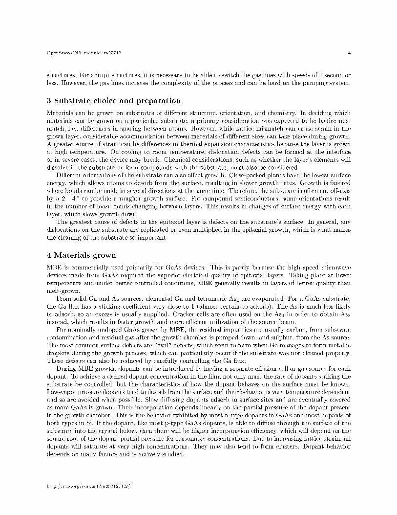
In the process of epitaxy, a thin layer of material is grown on a substrate. With respect to crystal growthit applies to the process of growing thin crystalline layers on a crystal substrate. In epitaxial growth, thereis a precise crystal orientation of the �lm in relation to the substrate. For electronic devices, the substrateis a single crystal (usually Si or GaAs) and therefore so is the epitaxial layer (epilayer). In the most basicform of molecular beam epitaxy (MBE), the substrate is placed in ultra high vacuum (UHV) and the sourcematerials for the �lm are evaporated from elemental sources. The evaporated molecules or atoms �ow asa beam, striking the substrate, where they are adsorbed on the surface. Once on the surface, the atomsmove by surface di�usion until they reach a thermodynamically favorable location to bond to the substrate.Molecules will dissociate to atomic form during di�usion or at a favorable site. Figure 1 illustrates theprocesses that can occur on the surface. Because the atoms require time for surface di�usion, the quality ofthe �lm will be better with slower growth. Typically growth rates of about 1 monolayer per second providesu�ciently high quality.
*Version 1.2: Jul 13, 2009 5:36 pm -0500�http://creativecommons.org/licenses/by/3.0/
http://cnx.org/content/m25712/1.2/
OpenStax-CNX module: m25712 2
Figure 1: Schematic illustration of processes on growing surface during MBE. Adsorption of atoms onthe surface, surface di�usion of atoms, formation of crystalline lattice, desorption of particles from thesurface.
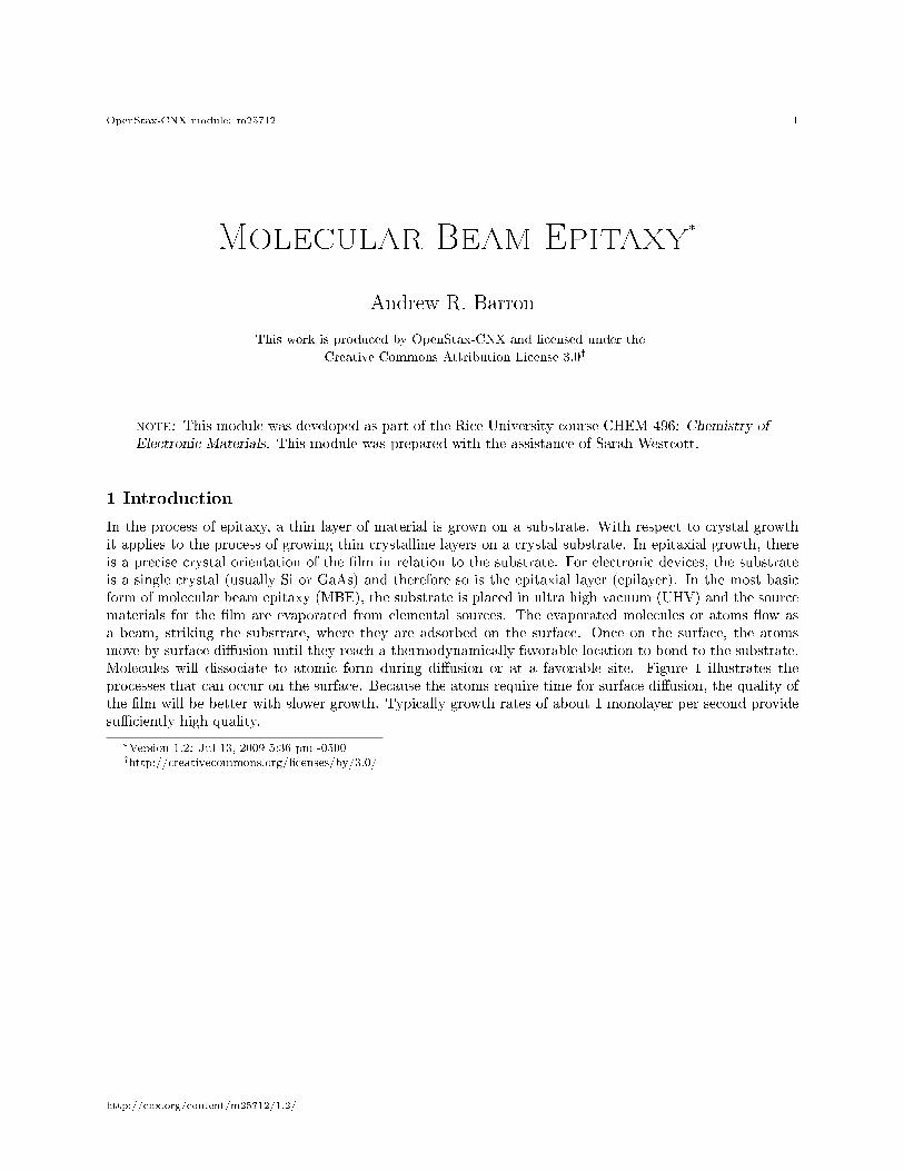
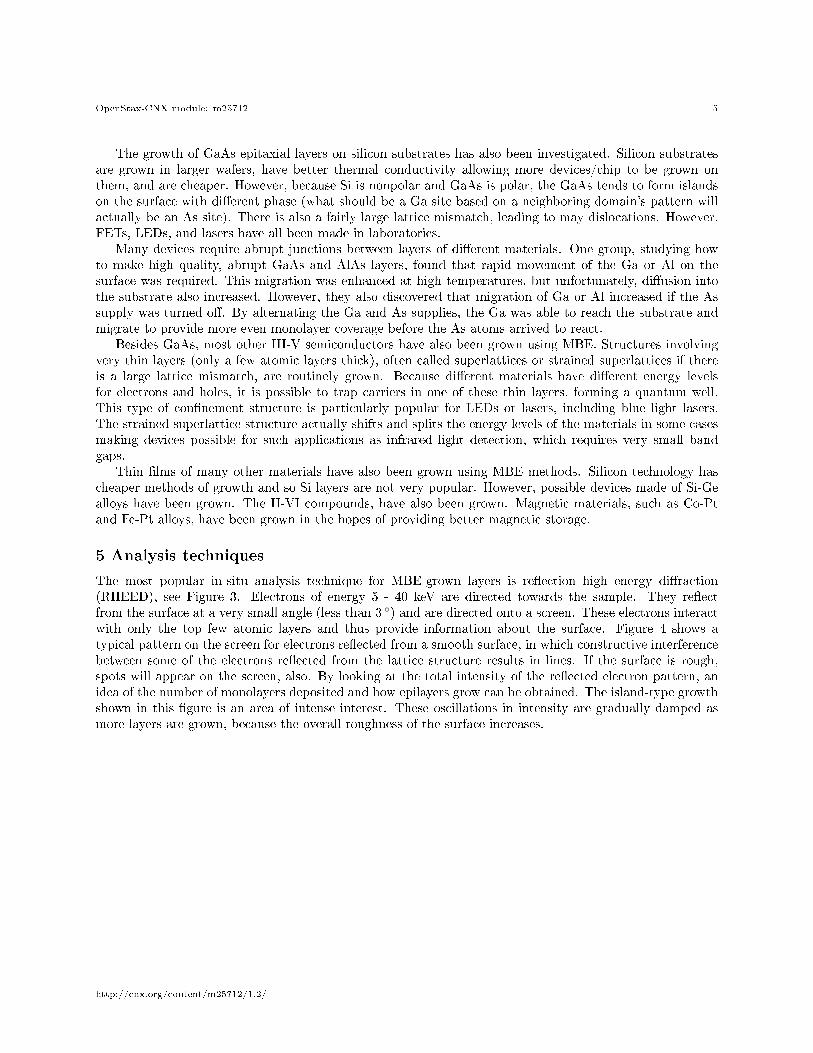
A typical MBE chamber is shown in Figure 2. The substrate is chemically washed and then put intoa loading chamber where it is further cleaned using argon ion bombardment followed by annealing. Thisremoves the top layers of the substrate, which is usually an undesired oxide which grew in air and containsimpurities. The annealing heals any damage caused by the bombardment. The substrate then enters thegrowth chamber via the sample exchange load lock. It is secured on a molybdenum holder either mechanicallyor with melted indium or gallium which hold the substrate by surface tension.
Figure 2: The MBE growth chamber.
Each e�usion cell (see Figure 2) is a source of one element in the �lm. The e�usion cell, also called a
http://cnx.org/content/m25712/1.2/
OpenStax-CNX module: m25712 3
Knudsen cell, contains the elemental form in very high purity (greater than 99.99999% for Ga and As). Thecell is heated to encourage evaporation. For GaAs growth, the temperature is typically controlled for a vaporpressure of 10-2 to 10-3 Torr inside the e�usion cell, which results in a transport of about 1015 molecules/cm2
to the substrate when the shutter for that cell is opened. The shape and size of the opening in the cell isoptimized for an even distribution of particles on the substrate. Due to the relatively low concentration ofmolecules, they typically do not interact with other molecules in the beam during the 5 - 30 cm journey tothe substrate. The substrate is usually rotated, at a few rpm, to further even the distribution.
Because MBE takes place in UHV and has relatively low pressure of residual gas at the surface, analysistechniques such as re�ection high energy di�raction and ellipsometry can be used during growth, bothto study and control the growth process. The UHV environment also allows pre or post growth analysistechniques such as Auger spectroscopy.
2 Elemental and molecular sources
The e�usion cell is used for the majority of MBE growth. All materials used in the cell are carefully chosento be noninteracting with the element being evaporated. For example, the crucible is pyrolitic boron nitride.However, it has disadvantages, such as:
• The evaporated species may be molecular, rather than monomeric, which will require further dissocationat the surface.
• When the shutter is opened, the heat loss from the cell results in a transient in the beam �ux whichlast for several minutes and cause variations of up to 50%.
• The growth chamber must be opened up to replace the solid sources.
Cracker cells are used to improve the ratio of monomeric to molecular (or at least dimeric to tetrameric)particles from the source. The cracker cell, placed so that the beam passes through it after the e�usion cell, ismaintained at a high temperature (and sometimes high pressure) to encourage dissociation. The dissociationprocess generally requires a catalyst and the best catalysts for a given species have been studied.
Some elements, such as silicon, have low enough vapor pressure that more direct heating techniques suchas electron bombardment or laser radiation heating are used. The electron beam is bent using electromagneticfocusing to prevent any impurities in the electron source from contaminating the silicon to be used in MBE.Because the heat is concentrated on the surface to be evaporated, interactions with and contamination fromthe crucible walls is reduced. In addition, this design does not require a shutter, so there is no problem withtransients. Modulation of the beam can produce very sharp interfaces on the substrate. In laser radiationheating, the electron beam is replaced by a laser beam. The advantages of localized heating and rapidmodulation are also maintained without having to worry about contamination from the electron source orstray electrons.
Some of the II-VI (12-16) compounds have such high vapor pressure that a Knudson cell cannot be used.For example, the mercury source must be kept cooler than the substrate to keep the vapor pressure lowenough to be feasible. The Hg source must also be sealed o� from the growth chamber to allow the chamberto be pumped down.
Two other methods of obtaining the elements for use in epitaxy are gas-source epitaxy and chemical beamepitaxy (CBE). Both of these methods use gas sources, but they are distinguished by the use of elementalbeams in gas source epitaxy, while organometallic beams are used in CBE. For the example of III-V (13-15)semiconductors, in gas epitaxy, the group III material may come from an e�usion cell while the group Vmaterial is the hydride, such as AsH3 or PH3, which is cracked before entering the growth chamber. InCBE, the group V material is an organometallic, such as triethylgallium [Ga(C2H5)3] or trimethylaluminum[Al(CH3)3], which adsorbs on the surface, where it dissociates.
The gas sources have several advantages. Gas lines can be run into the chamber, which allows the supplyto be replenished without opening the chamber. When making alloys, such as AlxGa1-xAs, the gases can bepremixed for the correct stochiometry or even have their composition gradually changed for making graded
http://cnx.org/content/m25712/1.2/
OpenStax-CNX module: m25712 4
structures. For abrupt structures, it is necessary to be able to switch the gas lines with speeds of 1 second orless. However, the gas lines increase the complexity of the process and can be hard on the pumping system.
3 Substrate choice and preparation
Materials can be grown on substrates of di�erent structure, orientation, and chemistry. In deciding whichmaterials can be grown on a particular substrate, a primary consideration was expected to be lattice mis-match, i.e., di�erences in spacing between atoms. However, while lattice mismatch can cause strain in thegrown layer, considerable accommodation between materials of di�erent sizes can take place during growth.A greater source of strain can be di�erences in thermal expansion characteristics because the layer is grownat high temperature. On cooling to room temperature, dislocation defects can be formed at the interfaceor in severe cases, the device may break. Chemical considerations, such as whether the layer's elements willdissolve in the substrate or form compounds with the substrate, must also be considered.
Di�erent orientations of the substrate can also a�ect growth. Close-packed planes have the lowest surfaceenergy, which allows atoms to desorb from the surface, resulting in slower growth rates. Growth is favoredwhere bonds can be made in several directions at the same time. Therefore, the substrate is often cut o�-axisby a 2 - 4 ◦ to provide a rougher growth surface. For compound semiconductors, some orientations resultin the number of loose bonds changing between layers. This results in changes of surface energy with eachlayer, which slows growth down.
The greatest cause of defects in the epitaxial layer is defects on the substrate's surface. In general, anydislocations on the substrate are replicated or even multiplied in the epitaxial growth, which is what makesthe cleaning of the substrate so important.
4 Materials grown
MBE is commercially used primarily for GaAs devices. This is partly because the high speed microwavedevices made from GaAs required the superior electrical quality of epitaxial layers. Taking place at lowertemperature and under better controlled conditions, MBE generally results in layers of better quality thanmelt-grown.
From solid Ga and As sources, elemental Ga and tetrameric As4 are evaporated. For a GaAs substrate,the Ga �ux has a sticking coe�cient very close to 1 (almost certain to adsorb). The As is much less likelyto adsorb, so an excess is usually supplied. Cracker cells are often used on the As4 in order to obtain As2instead, which results in faster growth and more e�cient utilization of the source beam.
For nominally undoped GaAs grown by MBE, the residual impurities are usually carbon, from substratecontamination and residual gas after the growth chamber is pumped down, and sulphur, from the As source.The most common surface defects are "oval" defects, which seem to form when Ga manages to form metallicdroplets during the growth process, which can particularly occur if the substrate was not cleaned properly.These defects can also be reduced by carefully controlling the Ga �ux.
During MBE growth, dopants can be introduced by having a separate e�usion cell or gas source for eachdopant. To achieve a desired dopant concentration in the �lm, not only must the rate of dopants striking thesubstrate be controlled, but the characteristics of how the dopant behaves on the surface must be known.Low-vapor pressure dopants tend to desorb from the surface and their behavior is very temperature dependentand so are avoided when possible. Slow di�using dopants adsorb to surface sites and are eventually coveredas more GaAs is grown. Their incorporation depends linearly on the partial pressure of the dopant presentin the growth chamber. This is the behavior exhibited by most n-type dopants in GaAs and most dopants ofboth types in Si. If the dopant, like most p-type GaAs dopants, is able to di�use through the surface of thesubstrate into the crystal below, then there will be higher incorporation e�ciency, which will depend on thesquare root of the dopant partial pressure for reasonable concentrations. Due to increasing lattice strain, alldopants will saturate at very high concentrations. They may also tend to form clusters. Dopant behaviordepends on many factors and is actively studied.
http://cnx.org/content/m25712/1.2/
OpenStax-CNX module: m25712 5
The growth of GaAs epitaxial layers on silicon substrates has also been investigated. Silicon substratesare grown in larger wafers, have better thermal conductivity allowing more devices/chip to be grown onthem, and are cheaper. However, because Si is nonpolar and GaAs is polar, the GaAs tends to form islandson the surface with di�erent phase (what should be a Ga site based on a neighboring domain's pattern willactually be an As site). There is also a fairly large lattice mismatch, leading to may dislocations. However,FETs, LEDs, and lasers have all been made in laboratories.
Many devices require abrupt junctions between layers of di�erent materials. One group, studying howto make high quality, abrupt GaAs and AlAs layers, found that rapid movement of the Ga or Al on thesurface was required. This migration was enhanced at high temperatures, but unfortunately, di�usion intothe substrate also increased. However, they also discovered that migration of Ga or Al increased if the Assupply was turned o�. By alternating the Ga and As supplies, the Ga was able to reach the substrate andmigrate to provide more even monolayer coverage before the As atoms arrived to react.
Besides GaAs, most other III-V semiconductors have also been grown using MBE. Structures involvingvery thin layers (only a few atomic layers thick), often called superlattices or strained superlattices if thereis a large lattice mismatch, are routinely grown. Because di�erent materials have di�erent energy levelsfor electrons and holes, it is possible to trap carriers in one of these thin layers, forming a quantum well.This type of con�nement structure is particularly popular for LEDs or lasers, including blue light lasers.The strained superlattice structure actually shifts and splits the energy levels of the materials in some casesmaking devices possible for such applications as infrared light detection, which requires very small bandgaps.
Thin �lms of many other materials have also been grown using MBE methods. Silicon technology hascheaper methods of growth and so Si layers are not very popular. However, possible devices made of Si-Gealloys have been grown. The II-VI compounds, have also been grown. Magnetic materials, such as Co-Ptand Fe-Pt alloys, have been grown in the hopes of providing better magnetic storage.
5 Analysis techniques
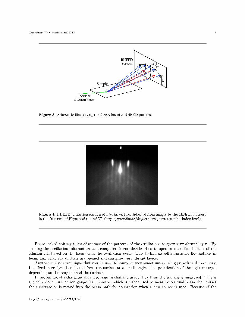
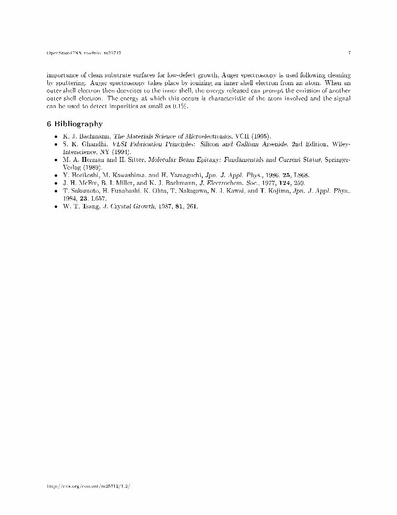
The most popular in-situ analysis technique for MBE-grown layers is re�ection high energy di�raction(RHEED), see Figure 3. Electrons of energy 5 - 40 keV are directed towards the sample. They re�ectfrom the surface at a very small angle (less than 3 ◦) and are directed onto a screen. These electrons interactwith only the top few atomic layers and thus provide information about the surface. Figure 4 shows atypical pattern on the screen for electrons re�ected from a smooth surface, in which constructive interferencebetween some of the electrons re�ected from the lattice structure results in lines. If the surface is rough,spots will appear on the screen, also. By looking at the total intensity of the re�ected electron pattern, anidea of the number of monolayers deposited and how epilayers grow can be obtained. The island-type growthshown in this �gure is an area of intense interest. These oscillations in intensity are gradually damped asmore layers are grown, because the overall roughness of the surface increases.
http://cnx.org/content/m25712/1.2/
OpenStax-CNX module: m25712 6
Figure 3: Schematic illustrating the formation of a RHEED pattern.
Figure 4: RHEED di�raction pattern of a GaAs surface. Adapted from images by the MBE Laboratoryin the Institute of Physics of the ASCR (http://www.fzu.cz/departments/surfaces/mbe/index.html).
Phase locked epitaxy takes advantage of the patterns of the oscillations to grow very abrupt layers. Bysending the oscillation information to a computer, it can decide when to open or close the shutters of thee�usion cell based on the location in the oscillation cycle. This technique self-adjusts for �uctuations inbeam �ux when the shutters are opened and can grow very abrupt layers.
Another analysis technique that can be used to study surface smoothness during growth is ellipsometry.Polarized laser light is re�ected from the surface at a small angle. The polarization of the light changes,depending on the roughness of the surface.
Improved growth characteristics also require that the actual �ux from the sources is measured. This istypically done with an ion gauge �ux monitor, which is either used to measure residual beam that missesthe substrate or is moved into the beam path for calibration when a new source is used. Because of the
http://cnx.org/content/m25712/1.2/
OpenStax-CNX module: m25712 7
importance of clean substrate surfaces for low-defect growth, Auger spectroscopy is used following cleaningby sputtering. Auger spectroscopy takes place by ionizing an inner shell electron from an atom. When anouter shell electron then deexcites to the inner shell, the energy released can prompt the emission of anotherouter shell electron. The energy at which this occurs is characteristic of the atom involved and the signalcan be used to detect impurities as small as 0.1%.
6 Bibliography
• K. J. Bachmann, The Materials Science of Microelectronics, VCH (1995).• S. K. Ghandhi, VLSI Fabrication Principles: Silicon and Gallium Arsenide, 2nd Edition, Wiley-
Interscience, NY (1994).• M. A. Herman and H. Sitter, Molecular Beam Epitaxy: Fundamentals and Current Status, Springer-
Verlag (1989).• Y. Horikoshi, M. Kawashima, and H. Yamaguchi, Jpn. J. Appl. Phys., 1986, 25, L868.• J. H. McFee, B. I. Miller, and K. J. Bachmann, J. Electrochem. Soc., 1977, 124, 259.• T. Sakamoto, H. Funabashi, K. Ohta, T. Nakagawa, N. J. Kawai, and T. Kojima, Jpn. J. Appl. Phys.,
1984, 23, L657.• W. T. Tsang, J. Crystal Growth, 1987, 81, 261.
http://cnx.org/content/m25712/1.2/