Embed Size (px)
Citation preview
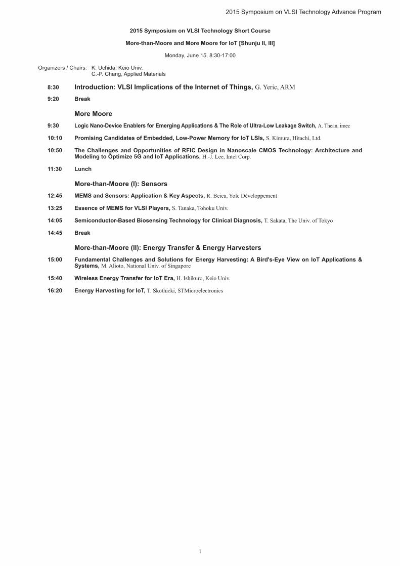
2015 Symposium on VLSI Technology Advance Program
2015 Symposium on VLSI Technology Short Course
More-than-Moore and More Moore for IoT [Shunju II, III]
Monday, June 15, 8:30-17:00
Organizers / Chairs: K. Uchida, Keio Univ. C.-P. Chang, Applied Materials
8:30 Introduction: VLSI Implications of the Internet of Things, G. Yeric, ARM
9:20 Break
More Moore 9:30 Logic Nano-Device Enablers for Emerging Applications & The Role of Ultra-Low Leakage Switch, A. Thean, imec
10:10 Promising Candidates of Embedded, Low-Power Memory for IoT LSIs, S. Kimura, Hitachi, Ltd.
10:50 The Challenges and Opportunities of RFIC Design in Nanoscale CMOS Technology: Architecture and Modeling to Optimize 5G and IoT Applications, H.-J. Lee, Intel Corp.
11:30 Lunch
More-than-Moore (I): Sensors 12:45 MEMS and Sensors: Application & Key Aspects, R. Beica, Yole Développement
13:25 Essence of MEMS for VLSI Players, S. Tanaka, Tohoku Univ.
14:05 Semiconductor-Based Biosensing Technology for Clinical Diagnosis, T. Sakata, The Univ. of Tokyo
14:45 Break
More-than-Moore (II): Energy Transfer & Energy Harvesters 15:00 Fundamental Challenges and Solutions for Energy Harvesting: A Bird's-Eye View on IoT Applications &
Systems, M. Alioto, National Univ. of Singapore
15:40 Wireless Energy Transfer for IoT Era, H. Ishikuro, Keio Univ.
16:20 Energy Harvesting for IoT, T. Skothicki, STMicroelectronics
1
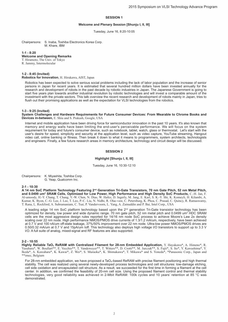
2015 Symposium on VLSI Technology Advance Program
SESSION 1
Welcome and Plenary Session [Shunju I, II, III]
Tuesday, June 16, 8:20-10:05
Chairpersons: S. Inaba, Toshiba Electronics Korea Corp. M. Khare, IBM
1-1 - 8:20Welcome and Opening RemarksT. Hiramoto, The Univ. of TokyoR. Jammy, Intermolecular
1-2 - 8:45 (Invited)Robotics for Innovation, H. Hirukawa, AIST, Japan
Robotics has been expected to solve serious social problems including the lack of labor population and the increase of senior persons in Japan for recent years. It is estimated that several hundred million dollars have been invested annually for the research and development of robots in the past decade by robotic industries in Japan. The Japanese Government is going to start five years plan towards another industrial revolution by robotic technologies and will invest a comparable amount of the investment with the private sectors. This talk overview the recent research and development of robots mainly in Japan, tries to flush out their promising applications as well as the expectation for VLSI technologies from the robotics.
1-3 - 9:25 (Invited)System Challenges and Hardware Requirements for Future Consumer Devices: From Wearable to Chrome Books and Devices in-between, E. Shiu and S. Prakash, Google, USA
Internet and mobile application have been driving force for semiconductor innovation in the past 10 years. It's also known that memory and energy walls have been limiting the end-user's perceivable performance. We will focus on the system requirement for today and future's consumer device, such as notebook, tablet, watch, glass or thermostat. Let's start with the user's desire for speed, simplicity and security at the application level, such as video capture, YouTube streaming, Hangout video call, online banking or fitness. Then break it down to what it means to programmers, system architects, technologists and engineers. Finally, a few future research areas in memory architecture, technology and circuit design will be discussed.
SESSION 2
Highlight [Shunju I, II, III]
Tuesday, June 16, 10:30-12:10
Chairpersons: K. Miyashita, Toshiba Corp. G. Yeap, Qualcomm Inc.
2-1 - 10:30A 14 nm SoC Platform Technology Featuring 2nd Generation Tri-Gate Transistors, 70 nm Gate Pitch, 52 nm Metal Pitch, and 0.0499 um2 SRAM Cells, Optimized for Low Power, High Performance and High Density SoC Products, C.-H. Jan, F. Al-amoody, H.-Y. Chang, T. Chang, Y.-W. Chen, N. Dias, W. Hafez, D. Ingerly, M. Jang, E. Karl, S. K.-Y. Shi, K. Komeyli, H. Kilambi, A. Kumar, K. Byon, C.-G. Lee, J. Lee, T. Leo, P.-C. Liu, N. Nidhi, R. Olac-vaw, C. Petersburg, K. Phoa, C. Prasad, C. Quincy, R. Ramaswamy, T. Rana, L. Rockford, A. Subramaniam, C. Tsai, P. Vandervoorn, L. Yang, A. Zainuddin and P. Bai, Intel Corp., USA
A leading edge 14 nm SoC platform technology based upon the 2nd generation Tri-Gate transistor technology has been optimized for density, low power and wide dynamic range. 70 nm gate pitch, 52 nm metal pitch and 0.0499 um2 HDC SRAM cells are the most aggressive design rules reported for 14/16 nm node SoC process to achieve Moore’s Law 2x density scaling over 22 nm node. High performance NMOS/PMOS drive currents of 1.3/1.2 mA/um, respectively, have been achieved at 0.7 V and 100 nA/um off-state leakage, 37%/50% improvement over 22 nm node. Ultra-low power NMOS/PMOS drives are 0.50/0.32 mA/um at 0.7 V and 15pA/um Ioff. This technology also deploys high voltage I/O transistors to support up to 3.3 V I/O. A full suite of analog, mixed-signal and RF features are also supported.
2-2 - 10:55Highly Reliable TaOx ReRAM with Centralized Filament for 28-nm Embedded Application, Y. Hayakawa*, A. Himeno*, R. Yasuhara*, W. Boullart**, E. Vecchio**, T. Vandeweyer**, T. Witters**, D. Crotti**, M. Jurczak**, S. Fujii*, S. Ito*, Y. Kawashima*, Y. Ikeda*, A. Kawahara*, K. Kawai*, Z. Wei*, S. Muraoka*, K. Shimakawa*, T. Mikawa* and S. Yoneda*, *Panasonic Corp., Japan and **imec, Belgium
For 28-nm embedded application, we have proposed a TaOx-based ReRAM with precise filament positioning and high thermal stability. The cell was realized using several newly-developed process technologies and cell structures: low-damage etching, cell side oxidation and encapsulated cell structure. As a result, we succeeded for the first time in forming a filament at the cell center. In addition, we confirmed the feasibility of 20-nm cell size. Using the proposed filament control and thermal stability technologies, very good reliability was achieved in 2-Mbit ReRAM: 100k cycles and 10 years’ retention at 85 °C was demonstrated.
2
2015 Symposium on VLSI Technology Advance Program
2-3 - 11:20High-Mobility High-Ge-Content Si1-xGex-OI PMOS FinFETs with Fins Formed Using 3D Germanium Condensation with Ge Fraction Up to x~ 0.7, Scaled EOT~8.5Å and ~10nm Fin Width, P. Hashemi, T. Ando, K. Balakrishnan, J. Bruley, S. Engelmann, J. A. Ott, V. Narayanan, D.-G. Park, R. T. Mo and E. Leobandung, IBM T. J. Watson Research Center, USA
We demonstrate scaled High-Ge-Content (HGC) SiGe-OI finFET with Ge up to 71%, using a CMOS-compatible approach. For the first time, aggressively scaled HGC relatively-tall fins with vertical sidewalls and sub-10nm widths have been demonstrated using an enhanced 3D-Ge-condensation technique. An improved Si-cap-free HK/MG process featuring optimized IL has been developed resulting in scaled EOT and impressive long channel SS=69mV/dec. The gate stack results in realization of enhancement-mode devices for Ge content ~0.6. Moreover, long-channel mobility characteristics at scaled EOT as well as short-channel pMOS FinFETs with decent cut-off behavior and performance are demonstrated, for the first time. As a result, we report the highest HGC SiGe pMOS FinFET mobility of ~300cm2/Vs at Ninv=1013cm-2 at scaled EOT=0.85nm.
2-4 - 11:45Design and Demonstration of Reliability-Aware Ge Gate Stacks with 0.5 nm EOT, C. Lu*,**, C. H. Lee*,**, T. Nishimura*,** and A. Toriumi*,**, *The Univ. of Tokyo and **JST-CREST, Japan
This paper reports a novel material/process-based design for reliability-aware Ge gate stack for the first time. Initially good characteristics of Ge gate stacks do not necessarily guarantee the long-term device reliability. To overcome the big hurdle, we have investigated the stability of GeO2 network as well as the formation of new high-k. The very robust Ge gate stack with both 0.5 nm EOT and sufficiently low Dit is demonstrated.
SESSION 3
Technology Focus Session - 7nm Node Logic Technology and Beyond [Shunju II, III]
Tuesday, June 16, 13:30-15:35
Chairpersons: M. Masahara, AIST R. Arghavani, LAM Research
3-1 - 13:30 (Invited)III-V and Ge Tunneling FET Technologies for Low Power LSIs, S. Takagi*,**, M.-S. Kim*,**, M. Noguchi*, S.-M. Ji*,**, K. Nishi*,** and M. Takenaka*,**, *The Univ. of Tokyo and **JST-CREST, Japan
We have demonstrated high performance operation of planar-type tunnel field-effect transistors (TFETs) using Ge/III-V materials. Tensile strain in Si channels combined with the Ge source can enhance the tunneling current because of the reduced effective energy bandgap. The fabricated Ge/sSOI (1.1 %) TFETs show high Ion/Ioff ratio over 107 and steep minimum subthreshold slope (SS) of 28 mV/dec. It is found that Ion and SS are improved by positive back bias. We have also demonstrated the operation of high Ion/Ioff and low SS planar-type InGaAs Tunnel FETs with Zn-diffused source junctions. Solid-phase Zn diffusion can realize steep-profile and defect-less p+/n source junctions. The small S.S. of 64 mV/dec and large Ion/Ioff ratio over 106 have been realized in the planar-type III-V TFETs.
3-2 - 13:55Variation-Tolerant Dense TFET Memory with Low VMIN Matching Low-Voltage TFET Logic, D. H. Morris, U. E. Avci and I. A. Young, Intel Corp., USA
The tunneling FET (TFET) is a leading option for energy efficient computation with peak logic performance/watt greater than CMOS. With variation effects, TFET reaches 2X higher peak efficiency than MOSFET by using supply voltages under 0.4V. Dense TFET SRAM bitcell is proposed with VMIN matching this low logic VDD. Projections of device variation enable a comparison of TFET and MOSFET logic and memory and show greater robustness for TFET circuits. TFET bitcell write-time tracks logic frequency at low voltage. TFET bitcell retention margins are 0.1 V greater than that of the MOSFET. Bitcell performance and VMIN are improved by using TFET’s unique asymmetric conduction to reduce write-contention and read-disturb conditions. A novel 7T bitcell with compact layout is proposed for improved low-voltage write.
3-3 - 14:20 (Invited)Vertical Device Architecture for 5nm and Beyond: Device and Circuit Implications, A. V.-Y. Thean, D. Yakimets, T. H. Bao, P. Schuddinck, S. Sakhare, M. G. Bardon, A. Sibaja-Her-nandez, G. Eneman, A. Veloso, J. Ryckaert, P. Raghavan, A. Mercha, A. Mocuta, Z. Tokei, D. Verkest, P. Wambacq, K. De Meyer and N. Collaert, imec, Belgium
Vertical nanowire logic circuits may enable density scaling well beyond lateral CMOS layouts limited by gate and contact place-ment. In this paper, we compared the performance, layout effi-ciency, SRAM design, and parasitics between vertical (VFETs) gate-all-around (GAA) transistors with lateral (LFETs) targeting 5nm. We reviewed some of the unique considerations of VFET device and circuit influences.
3-4 - 14:4515-nm Channel Length MoS2 FETs with Single- and Double-Gate Structures, A. Nourbakhsh*,**, A. Zubair*, S. Huang*, X. Ling*, M. S. Dresselhaus*, J. Kong*, S. De Gendt**,*** and T. Palacios*, *Massachusetts Institute of Technology, USA, **imec and ***KU Leuven, Belgium
We demonstrate single- and double-gated (SG & DG) field effect transistors (FETs) with a record source-drain length (LS/D) of 15 nm built on monolayer (tch~0.7 nm) and 4-layer (tch~3 nm) MoS2 channels using monolayer graphene as the Source/Drain contacts. The best devices, corresponding to DG 4-layer MoS2-FETs with LS/D=15 nm, had an Ion/Ioff in excess of 106 and a minimum subthreshold swing (SSmin.) of 90 mV/dec. at VDS=0.5 V. At LS/D=1 μm and VDS=0.5 V, SSmin.=66 mV/dec., which is the best SS reported in MoS2 FETs, indicating the high quality of the interface and the enhanced channel electrostatics.
3
2015 Symposium on VLSI Technology Advance Program
3-5 - 15:10A Comparison of Arsenic and Phosphorus Extension by Room Temperature and Hot Ion Implantation for NMOS Si Bulk-FinFET at N7 (7nm) Technology Relevant Fin Dimensions, Y. Sasaki*, R. Ritzenthaler*, A. De Keersgieter*, T. Chiarella*, S. Kubicek*, E. Rosseel*, A. Waite***, J. del Agua Borniquel**, B. Colombeau***, S. A. Chew*, M. S. Kim*, T. Schram*, S. Demuynck*, W. Vandervorst*, N. Horiguchi*, D. Mocuta*, A. Mocuta* and A. V.-Y. Thean*, *imec, **Applied Materials Belgium, Belgium and ***Applied Materials, USA
We compare As and P extension implants for NMOS Si bulk FinFETs with 5nm wide fins. P implanted FinFETs shows improved ION, +15% with Room Temperature (RT) ion implantation (I/I) and +9% with hot I/I, keeping matched Short Channel Effects (SCE) for gate length (LG) of 30nm compared with As implanted FinFETs. Based on TCAD work, P increases activated dopant concentration in extension compared with As and 5nm fin suppresses off state leakage current under the gate efficiently even in P extension case though P diffusion is faster than As.
SESSION 4
Reliability [Shunju I]
Tuesday, June 16, 13:30-15:35
Chairpersons: B. H. Lee, Gwangju Institute of Science and Technology T. Ernst, CEA-LETI
4-1 - 13:30AC NBTI of Ge pMOSFETs: Impact of Energy Alternating Defects on Lifetime Prediction, J. Ma*, W. Zhang*, J. F. Zhang*, Z. Ji*, B. Benbakhti*, J. Franco**, J. Mitard**, L. Witters**, N. Collaert** and G. Groeseneken**, *Liverpool John Moores Univ., UK and **imec, Belgium
Ge pMOSFETs are strong candidates for next technology nodes due to its high hole mobility. Their reliability was studied under DC stress, but not under AC stress yet. For Si devices, industry can predict AC NBTI lifetime from DC stress after introducing a measurement delay either purposely or implicitly by using slow measurement as both agree well at effective stress time, because degradation under AC is the same as DC after a delay-induced recovery. The significance of this work is that, for the first time, we report that AC lifetime for Ge is much longer than DC even after a long measurement delay, and the AC lifetime MUST NOT be predicted from DC stress as used in Si, since overdrive voltage can be underestimated by 0.5V. A key advance of this work is the understanding of this important difference between Si and Ge and identifying the responsible defects and mechanism.
4-2 - 13:55A Test-Proven As-Grown-Generation (A-G) Model for Predicting NBTI under Use-Bias, Z. Ji*, J. F. Zhang*, L. Lin*, M. Duan*, W. Zhang*, X. Zhang*, R. Gao*, B. Kaczer**, J. Franco**, T. Schram**, N. Horiguchi**, S. De Gendt** and G. Groeseneken**, *Liverpool John Moores Univ., UK and **imec, Belgium
The gap between modelling and real performance has been identified as a major constraint for design optimisation and the inaccuracy of NBTI models contributes to it. For the first time, we demonstrate that A-G model extracted from short Vg-accelerated stresses can predict both long term DC and AC NBTI under low and dynamic operation Vg. This is achieved by successfully separating non-saturating defects from the saturating ones, allowing reliable extraction of power exponents needed for long term prediction. A-G model does not require solving differential equations for prediction. This saves computation time significantly, especially for high-frequency that needs small time-step, and makes it readily implementable in SPICE-like simulators.
4-3 - 14:20Impact of Random Telegraph Noise on Write Stability in Silicon-on-Thin-BOX (SOTB) SRAM Cells at Low Supply Voltage in Sub-0.4V Regime, H. Qiu*, T. Mizutani*, Y. Yamamoto**, H. Makiyama**, T. Yamashita**, H. Oda**, S. Kamohara**, N. Sugii**, T. Saraya*, M. Kobayashi* and T. Hiramoto*, *The Univ. of Tokyo and **LEAP, Japan
The effect of random telegraph noise (RTN) on write stability of SRAM cells in sub-0.4V operation is intensively measured and statistically analyzed. RTN of N-curves in Silicon-on-Thin-BOX (SOTB) cells is monitored. By developing statistical models, it is found that, different from bulk SRAM cells operating at high supply voltage (VDD), fail bit rate (FBR) at sub-0.4V is degraded by RTN. The origin of high FBR due to RTN at sub-0.4V is discussed.
4-4 - 14:45Further Investigations on Traps Stabilities in Random Telegraph Signal Noise and the Application to a Novel Concept Physical Unclonable Function (PUF) with Robust Reliabilities, J. Chen, T. Tanamoto, H. Noguchi and Y. Mitani, Toshiba Corp., Japan
A novel physical unclonable function (PUF) that based on random telegraph signal noise (RTN) is proposed and studied in this work. Firstly, systematical experiments have been done in ultra-scaled devices with various gate stack structures. It is found for the first time that strong correlations between trap time constants and thermal activation energies universally exist in all devices, no matter for hole traps or for electron traps, in high-k dielectrics or in SiO2. More importantly, time constants are stress free and quite stable under electrical stressing. Then, with proposed transient RTN approaches and algorithms, RTN related traps can be detected in a short time and directly utilized in PUF designs. The hamming distance (HD) of intra-PUF and inter-PUF is experimentally characterized, showing excellent endurance properties with no less than 1E6 ID reading cycles.
4
2015 Symposium on VLSI Technology Advance Program
4-5 - 15:10High Frequency AC Electromigration Lifetime Measurements from a 32nm Test Chip, C. Zhou*, X. Wang**, R. Fung***, S.-J. Wen****, R. Wong**** and C. H. Kim*, *Univ. of Minnesota, **Intel Corp., USA, ***Cisco Systems, Inc., China and ****Cisco Systems, Inc., USA
A test circuit for studying Electromigration (EM) effects under realistic high frequency AC stress was implemented in a 32nm High-k Metal Gate (HKMG) process. Four different stress patterns (DC, pulsed DC, square AC and real AC) can be generated using on-chip circuits. Local heaters are used to raise the die temperature to >300°C for accelerated testing. Experiment results over 52.7 hours show no AC stress induced failures under 325°C, 1.5V (driver supply) at 200 MHz and 900 MHz. However, the pre-AC stress had an impact on the DC EM distribution.
SESSION 5
Technology Focus Session - 3D Systems and Packaging [Shunju II, III]
Tuesday, June 16, 15:50-17:30
Chairpersons: Y.-C. Yeo, TSMC J. Cheek, Freescale
5-1 - 15:50 (Invited)A New Integration Technology Platform: Integrated Fan-Out Wafer-Level-Packaging for Mobile Applications, D. Yu, TSMC, Taiwan
3D sub-system integration of logic and DRAM with TSV is desirable for wide memory bandwidth and reduced power for mobile applications. However, its manufacturing cost, along with testing and heat dissipation, remains to be outstanding issues. A new integration technology platform, InFO, is proposed to address it. In this paper, we compare three main 3D integration architectures: InFO_PoP, FC_PoP and 3DIC with TSV based on mobile product requirements, including system power- performance-profile (form factor), heat dissipation, memory bandwidth and production cycle-time along with cost. InFO not only best optimizes and achieves the requirements, but also more readily integrates partitioned-chips, which further impacts on the manufacturing of the logic/DRAM sub-system.
5-2 - 16:15 (Invited)3D VLSI-CoolCube Process: An Alternative Path to Scaling, P. Batude*, C. Fenouillet-Beranger*, L. Pasini*,**,***, V. Lu*,**, F. Deprat*,***, M. Cassé*, B. Mathieu*, B. Sklenard*, F. Piegas-Luce*, O. Billoint*, O. Turkyilmaz*, H. Sarhan*, S. Sollier*, J. Widiez*, C. Tabone*, M.-P. Samson*, B. Previtali* , N. Rambal*, F. Ponthenier*, J. Mazurier*, R. Beneyton**, M. Bidaud**, E. Josse**, E. Petitprez**, O. Rozeau*, S. Martini*, L. Brunet*, M. Rivoire**, C. Euvard-Colnat*, A. Seignard*, F. Fournel*, L. Benaissa*, J.-M. Hartmann*, P. Besson**, S. Kerdiles*, C. Bout*, F. Nemouchi*, A. Royer*, G. Ghibaudo***, T. Signamarcheix*, M. Haond**, F. Clermidy*, O. Faynot* and M. Vinet*, *CEA-LETI, **STMicroelectronics and ***IMEP-LAHC, France
3D VLSI in a CoolCubeTM integration allows stacking several layers of devices on top of each other with a unique connecting via density above a million/mm². It is shown to enable density increase at no transistor scaling cost, while benefiting from gain in power and performance thanks to wire-length reduction. CoolCube technology leads to high performance top transistors with Thermal Budget (TB) compatible with bottom MOSFET integrity; Key enablers are the dopant activation by Solid Phase Epitaxy (SPE) or Nanosecond Laser Anneal (NSA), low temperature epitaxy, low k spacers and direct bonding. Data on bottom MOSFET maximum TB (with high temperatures but short durations) offers new opportunities for top MOSFET process optimization.
5-3 - 16:40High Performance Low Temperature Activated Devices and Optimization Guidelines for 3D VLSI Integration of FD, TriGate, FinFET on Insulator, L. Pasini*,**,***, P. Batude*, M. Cassé*, B. Mathieu*, B. Sklenard*, F. P. Luce*, S. Reboh*, N. Bernier*, C. Tabone*, O. Rozeau*, S. Martini*, C. Fenouillet-Beranger*, L. Brunet*, G. Audoit*, D. Lafond*, F. Aussenac*, F. Allain*, G. Romano**, S. Barraud*, N. Rambal*, V. Barral*, L. Hutin*, J.-M. Hartmann*, P. Besson**, S. Kerdiles*, M. Haond**, G. Ghibaudo*** and M. Vinet*, *CEA-LETI, **STMicroelectronics and ***IMEP-LAHC, France
3D VLSI integration is a promising alternative path towards CMOS scalability. It requires Low Temperature (LT) processing (≤600°C) for top FET fabrication. In this work, record performance is demonstrated for LT TriGate and FDSOI devices using Solid Phase Epitaxy (SPE). Optimization guidelines for further performance improvement are given for FD, TriGate and FinFET on insulator with the constraint of 14nm node channel strain preservation. This work concludes that extension first process scheme (implantation before the raised source and drain epitaxy) is required for FDSOI and TriGate architectures.
5-4 - 17:05Ultra Fine-Pitch TSV Technology for Ultra-Dense High-Q RF Inductors, W. A. Vitale*, M. Fernández-Bolaños*, A. Klumpp**, J. Weber**, P. Ramm** and A. M. Ionescu*, *EPFL, Switzerland and **Fraunhofer EMFT, Germany
We demonstrate that fine-pitch TSV technology can be exploited to fabricate micro-inductors on high resistivity substrate, with record-high inductance per area and preserving their performance at GHz frequencies. We report an extensive experimental study on the effects of dimensional scaling and passive device density on RF performance of out-of-plane inductors exploiting W-based TSVs, with pitches down to 10 μm. We show wideband RF inductors with an unprecedented combination of a quality factor peak of 7.8 at 13 GHz, self-resonance frequency of 29.2 GHz, and inductance density of 124.4 nH/mm2. The reported technology also includes low loss interconnects, fixed capacitors and LC tanks, design to serving high performance 3D-integrated RF functionalities.
5
2015 Symposium on VLSI Technology Advance Program
SESSION 6
Advanced CMOS Technology: Ge FinFET / Compact Model [Shunju I]
Tuesday, June 16, 15:50-17:30
Chairpersons: S.Takagi, The Univ. of Tokyo P. D. Ye, Purdue Univ.
6-1 - 15:50Strained Germanium Quantum Well p-FinFETs Fabricated on 45nm Fin Pitch Using Replacement Channel, Replacement Metal Gate and Germanide-Free Local Interconnect, L. Witters, J. Mitard, R. Loo, S. Demuynck, S. A. Chew, T. Schram, Z. Tao, A. Hikavyy, J. W. Sun, A. P. Milenin, H. Mertens, C. Vrancken, P. Favia, M. Schaekers, H. Bender, N. Horiguchi, R. Langer, K. Barla, D. Mocuta, N. Collaert and A. V.-Y. Thean, imec, Belgium
Strained Ge p-channel FinFETs on Strain Relaxed SiGe are integrated for the first time on high density 45nm Fin pitch using a replacement channel approach on Si substrate. In comparison to our previous work on isolated sGe FinFETs [1], 14/16nm technology node compatible modules such as replacement metal gate and germanide-free local interconnect were implemented. The ION/IOFF benchmark shows the high density strained Ge pFinFETs in this work outperform the best published isolated strained Ge on SiGe devices.
6-2 - 16:15First Experimental Demonstration of Ge 3D FinFET CMOS Circuits, H. Wu, W. Luo, H. Zhou, M. Si, J. Zhang and P. D. Ye, Purdue Univ., USA
We report the first experimental demonstration of Ge 3D CMOS circuits, based on the recessed fin structure. Both n-FinFETs and p-FinFETs with channel length from 200 to 20 nm and fin width from 60 to 10 nm are realized on a Ge-on-insulator (GeOI) substrate. The Ge FinFETs show superior gate electrostatic control over planar devices and sub-threshold slope as low as 93 and 73 mV/dec are obtained on n- and p-FETs, respectively. Combining the n- and p- type 3D devices together, the FinFET CMOS inverters have high voltage gain up to 34 V/V at VDD of 1.4 V, delivering more than 200% improvement over the planar ones at the same channel length of 200 nm. Scalability studies are also carried out for both types of FinFETs in terms of channel length and fin width.
6-3 - 16:40Characterization of Self-Heating in High-Mobility Ge FinFET pMOS Devices, E. Bury*,**, B. Kaczer*, J. Mitard*, N. Collaert*, N. S. Khatami***, Z. Aksamija***, D. Vasileska****, K. Raleva*****, L. Witters*, G. Hellings*, D. Linten*, G. Groeseneken*,** and A. Thean*, *imec, **KU Leuven, Belgium, ***Univ. of Massachusetts-Amherst, ****Arizona State Univ., USA and *****“Ss Cyril and Methodius” Univ., Macedonia
Based on physically-extended methodology, measurements and simulations show that implementing high-mobility materials and particularly alloys, such as a SiGe buffer for mobility enhancement in a Ge channel, can result in a 115% increase in self heating in the N7 node, compared to standard Si FinFETs.
6-4 - 17:05New Industry Standard FinFET Compact Model for Future Technology Nodes, S. Khandelwa, J. P. Duarte, A. Medury, Y. S. Chauhan and C. Hu, Univ. of California, Berkeley, USA
A new production ready compact model for future FinFETs is presented. This single unified model can model FinFETs with realistic fin shapes including rectangle, triangle, circle and any shape in between. New mobility models support Ge p-FinFETs and InGaAs n-FinFETs. A new quantum effects model enables accurate modeling of III-V FinFETs. Special attention is paid to shape agnostic short-channel effect model for aggressive Lg scaling and body bias model for FinFETs on bulk substrates. With its accuracy verified with experimental data and TCAD, this computationally efficient model is an ideal turn-key solution for simulation and design of future heterogeneous circuits.
IEEE Solid-States Circuits Society Young Professionals and Grad Students Mentoring and Career coaching event [Suzaku III]
Tuesday, June 16, 17:30-18:30
This will be a special event for early career engineers and grad students, where several leading experts from industry and academia, IEEE Solid-States Circuits Society Executives and AdCom members will have a mentoring session on career coaching, entrepreneurship, publications and answer your questions. This special opportunity would be quite beneficial for the careers of young engineers and students.
Symposium on VLSI Technology
35th Anniversary Celebration [Shunju II, III]
Tuesday, June 16, 19:30-20:00
Alcoholic and Non-Alcoholic beverages will be served. Both Technology/Circuits Symposia attendees are cordially invited.
6
2015 Symposium on VLSI Technology Advance Program
Technology / Circuits Joint Evening Panel Discussion
Semiconductor Industry in 2020: Evolution or Revolution? [Shunju II, III]
Tuesday, June 16, 20:00-22:00
Organizers: N. Sugii, Hitachi, Ltd. G. Jurczak, imec M. Yamaoka, Hitachi, Ltd. A. Molnar, Cornell Univ. Moderators: T. Piliszczuk, Soitec J. Tham, Broadcom Corp.
Panelists: O. Nalamasu, Applied Materials J. Hausner, Intel Mobile S. Tanaka, Murata T. Yamauchi, Renesas S. Sivaram, SanDisk C. Diaz, TSMC W. Dai, VeriSilicon
Emerging markets such as IoT, M2M, and Big Data analysis will change the game rules of semiconductor industry in 2020. What kind of business models will be required for the players? It is becoming difficult for the Integrated Device Manufacturers (IDM) to make profits simply by fabricating devices. Not only the hardware, but services or solutions becomes more and more important. On the other hand, big players begins to put great effort on the LSI design and acquire many semiconductor design houses. Will the fabless be the best style in 2020? How foundry business will change? Panelists will present their opinions on this topic and discuss what is semiconductor industry in 2020.
Technology Evening Panel Discussion
Post Scaling: What Will be Next? [Suzaku I, II]
Tuesday, June 16, 20:00-22:00
Organizers: N. Sugii, Hitachi, Ltd. G. Jurczak, imec
Moderators: A. Nishiyama, Toshiba Corp. F. Boeuf, STMicroelectronics
Panelists: M. Vinet, CEA-LETI E. Shiu, Google A. Kumar, IBM A. Thean, imec J. Ohta, Nara Institute of Science & Technology T. Mogami, PETRA S. Mitra, Stanford Univ.
Continuous efforts have been made to extend the scaling of ULSIs for the enhancement of the performance of the devices. However, it is also true that the end of the scaling of MOSFETs and BEOL interconnect is coming in near future. Since it is believed that continuous performance improvements as well as new values of LSI systems are required even in the era of post-scaling, we have to find new ways to improve and extend the function of LSIs and those efforts could lead to the innovation of electronics. Considering the issue mentioned above, we invited several experts ranging from material and device level to system and architecture level. We would like to use this opportunity to discuss on 'What is the next? (What is the post-scaling technology?)' together with participants all over the world.
Circuits SESSION 1
Welcome and Plenary Session [Shunju I, II, III]
Wednesday, June 17, 8:30-10:05
Chairpersons: M. Motomura, Hokkaido Univ. G. Lehmann, Infineon Technologies AG
1-1 - 8:30Welcome and Opening RemarksH. Kabuo, Socionext Inc.J. Gealow, Analog Devices, Inc.
7
2015 Symposium on VLSI Technology Advance Program
1-2 - 8:45 (Invited)Profiting From IoT: The Key is Very-Large-Scale Happiness Integration, K. Yano, T. Akitomi, K. Ara, J. Watanabe, S. Tsuji, N. Sato, M. Hayakawa and N. Moriwaki, Hitachi, Ltd., Japan
Big data without link to value is merely a cost. We have studied how to profit from data with Internet-of-Things technologies for over 10 years to reach the answer: the Wearable Happiness Meter. It allows us to integrate the measure of both wellbeing and productivity of 7-billion people worldwide, which was the dream of the 18th-century philosopher Jeremy Bentham, numeration of the greatest happiness of the greatest number to measure the right and wrong. Knowing right and wrong with the 10x speed over conventional financial feedback accelerates the growth of the enterprise, the economy, and the individual to maximize the worldwide happiness. Here the integration is not only on the chip, but in the distributed massive chips embedded in the society.
1-3 - 9:25 (Invited)Automated Driving – Impacts on the Vehicle Architecture, M. Fausten, T. Huck, A. Rühle, T. Baysal, and R. Kornhaas, Robert Bosch GmbH, Germany
Automated Driving is currently one of the major trends in automotive industry. Almost every car maker has published a roadmap towards introducing automated driving in vehicles of their brand. Introduction of significant highly automated vehicles is expected within the next 10 years. Highly automated driving implies significant challenges to future control units. On the one hand side high performance is required to host the upcoming sophisticated SW which will evaluate the information of a multi sensor set, evaluate and interpret the current driving situation and finally take the decision about the vehicle behavior. On the other hand side, the control units have to be designed highly reliable and need to be composed into a fail operational vehicle architecture. The presentation will highlight the requirements for future electrical and electronics architectures of highly automated vehicles and discuss approaches how to fulfill these requirements.
Technology / Circuits Joint Focus Session 1
Ultra Low Power for IoT [Shunju II, III]
Wednesday, June 17, 10:30-12:35
Chairpersons: M. Tada, NEC Corp. G. Yeric, ARM
JFS1-1 - 10:30 (Invited)Automotive Low Power Technology for IoT Society, T. Yamauchi, H. Kondo and K. Nii, Renesas Electronics Corp., Japan
This paper addresses automotive low power technologies in Internet of Things (IoT) societies, where the interaction among cloud information, real-time recognition and vehicle control is a key. High reliability and high performance with low power under the harsh operating conditions are strongly demanded for automotive microcontroller units (MCUs). Our developed embedded Flash (eFlash) and SRAM achieved those required performance at up to Tj=170°C mainly for the vehicle control solution. To perform the highly robust computation in car information applications, the power management involving adaptive voltage scaling and real time power saving are adopted. Moreover other low-power schemes such as multi core CPUsystem with the easier parallelism and the digitally assisted ADC are introduced.
JFS1-2 - 10:55 (Invited)IoT: the Impact of Things, J. de Boeck*,**, *imec and **KU Leuven, Belgium
Starting from the application perspective this paper expands on the needs for sensor node architecture, wireless communication, security and infrastructure for IoT.
JFS1-3 - 11:20Transistor-Interconnect Mobile System-On-Chip Co-Design Method for Holistic Battery Energy Minimization, N. N. Mojumder, S. C. Song, K. Rim, J. Xu, J. Wang, J. Zhu, M. Vratonjic, K. Lin, M. Saint-Laurent, P. Bassett and G. Yeap, Qualcomm Technologies, Inc., USA
We present, first time, a holistic data-path-driven transistor-interconnect co-optimization method, which systematically isolates the logic-gate and interconnect-wire dominated data-paths in block-level-delay-bins (sub-binning of delay-based-bins) to significantly improve accuracy of static and dynamic power estimation. It captures the critical interdependence of transistor architecture (FEOL) including local interconnect, and BEOL metal stack optimization to achieve holistic 10nm (N10) technology optimization at target speeds. Using the proposed method, we drive >2.5x Performance/Watt (PpW) improvement for N10 FinFET SOC design over 14nm (N14). Even with ~3x higher wire resistance of min metal width, the PpW @target-speed for N10 improves >2.5x over N14 with proper design of metal/via stack, transistor Vt and fin-profile as well as standard-cell architecture. Reducing active fin-count and routing distance between standard-cells is a critical design knob for N10 mobile SOC enablement. The proposed methodology enables smartphone-usage (days-of-use) based technology optimization, driving longer battery-life in mobile SOCs, keeping process cost and complexity at minimum.
JFS1-4 - 11:45Sub-μW Standby Power, <18 μW/DMIPS@25MHz MCU with Embedded Atom-Switch Programmable Logic and ROM, Y. Tsuji, X. Bai, M. Miyamura, T. Sakamoto, M. Tada, N. Banno, K. Okamoto, N. Iguchi, N. Sugii and H. Hada, LEAP, Japan
A non-volatile programmable logic (NPL) with atom switch significantly accelerates performance of micro-controller unit (MCU). A low-power 32bit-CPU using a 65 nm-node Silicon-on-Thin-Box (SOTB) CMOS performs 1.95 DMIPS/MHz and 33 μW/MHz on 25 MHz and VDD=0.4 V. When a software process in the CPU is offloaded to NPL, the 9 times faster processing speed and 3 times higher energy efficiency are realized. A reverse body-bias on SOTB CMOS and a power-off of NPL block suppress a standby power down to 0.7 μW.
8

2015 Symposium on VLSI Technology Advance Program
JFS1-5 - 12:10 (Invited)Breakthrough Technologies and Reference Designs for New IoT Applications, P. Magarshack, STMicroelectronics, France
Internet of Things regroups numerous applications. Among those, a common critical point is definitely power, as well as energy efficiency. 28nm UTBB FDSOI (28FDSOI) has demonstrated its superiority in terms of energy efficiency through numerous publications. This paper demonstrates the extra mile 28FDSOI is able to offer to designers, enabling on one hand ultra-low power (ULP) system-on-chips for wearable and self-sustainable markets, as well as for medium performance and ultra-low power microprocessor units needed for data concentrators.
SESSION 7
Memory Technology: PC RAM [Shunju I]
Wednesday, June 17, 10:30-12:35
Chairpersons: H. Miyake, Micron Memory Japan K. Attenborough, NXP Central R&D
7-1 - 10:302.8-GB/s-Write and 670-MB/S-Erase Operations of a 3D Vertical Chain-Cell-Type Phase-Change-Memory Array, K. Kurotsuchi, Y. Sasago, H. Yoshitake, H. Minemura, Y. Anzai, Y. Fujisaki, T. Takahama, T. Takahashi, T. Mine, A. Shima, K. Fujisaki and T. Kobayashi, Hitachi, Ltd., Japan
A high-programming-throughput three-dimensional (3D) vertical chain-cell-type phase-change memory (VCCPCM) array for a next-generation storage device was fabricated. To increase the number of write cells at one time by reducing resistance of bit and source lines, the VCCPCM array includes plate electrodes and double-gate vertical-chain-selection MOSs with 5-nm-thick poly-Si channels. In addition, CO2 laser annealing enhances the drivability of a poly-Si cell MOS to 680 μA/μm to suppress energy loss in the cell MOS. In addition to write throughput, erase throughput is increased by erasing memory cells in a “bundle” by channel heating (called “bundle erase”). GeSbTe CVD with high uniformity is also developed.
7-2 - 10:55Greater than 2-bits/Cell MLC Storage for Ultra High Density Phase Change Memory Using a Novel Sensing Scheme, J. Y. Wu*, W. S. Khwa*, M. H. Lee*, H. P. Li*, S. C. Lai*, T. H. Su*, M. L. Wei*, T. Y. Wang*, M. BrightSky**, T. S. Chen*, W. C. Chien*, S. Kim**, R. Cheek**, H. Y. Cheng*, E. K. Lai*, Y. Zhu**, H. L. Lung* and C. Lam**, *Macronix International Co., Ltd., Taiwan and **IBM T. J. Watson Research Center, USA
Multi-level-cell (MLC) is a critical technology to achieve low bit cost for phase change memory. However, resistance drift is an intrinsic material property that kills memory window and imposes formidable challenges for MLC. In this work, we report a radically different sensing concept that exploits the non-linear R-V characteristics of PCM that can easily accommodate 8 resistance levels in three independent 10X sensing windows (100KΩ~1MΩ X 3) all on same read speed. Each sensing window only needs to store 2~3 resistance levels instead of 8 levels needed in conventional MLC method, thus can tolerate resistance drift without closing the memory windows. A maximum of 16 levels of MLC is demonstrated on a 256Mb chip that is suitable for 4-bits/cell application.
7-3 - 11:20A 50-nm 1.2-V GexTe1-x/Sb2Te3 Superlattice Topological-Switching Random-Access Memory (TRAM), M. Tai*, T. Ohyanagi*, M. Kinoshita*, T. Morikawa*, K. Akita*, M. Takato**, H. Shirakawa***, M. Araidai**, K. Shiraishi** and N. Takaura*, *LEAP, **Nagoya Univ. and ***Univ. of Tsukuba, Japan
A 50nm topological-switching random-access memory (TRAM) was fabricated for the first time. A high-quality GexTe1-x/Sb2Te3 superlattice film enabled set and reset voltages of TRAM to be less than 40% of those of PRAM. Statistical analysis of 16kb data showed the reset voltage to be less than 1.2 V, the lowest as a TRAM test chip.
7-4 - 11:45Operation Fundamentals in 12Mb Phase Change Memory Based on Innovative Ge-Rich GST Materials Featuring High Reliability Performance, V. Sousa*, G. Navarro*, N. Castellani*, M. Coué*, O. Cueto*, C. Sabbione*, P. Noé*, L. Perniola*, S. Blonkowski**, P. Zuliani*** and R. Annunziata***, *CEA-LETI, **STMicroelectronics, France and ***STMicroelectronics, Italy
For the first time, we present a Phase Change Memory (PCM) device with an optimized Ge-rich GeSbTe (GST) alloy integrated on a 12Mb test vehicle. We confirm that PCM can guarantee high data retention in extended temperature range and we provide the understanding of the high thermal stability of the two programmed states. We show how the elemental distribution reaches an equilibrium at the core of the storage element after the electrical activation of the cell, which relates to the strong opposition against crystallization of the RESET state. We also highlight the low number of grain boundaries along the conductive path of the optimized SET state, thus explaining the low drift of the resistance. Simulation results account for the experimental observations, showing how the segregation phenomena and the localization of the electronic switching impact the elemental distribution and the formation of the crystalline structure during programming.
7-5 - 12:10A Novel Self-Converging Write Scheme for 2-bits/Cell Phase Change Memory for Storage Class Memory (SCM) Application, W. C. Chien*, Y. H. Ho*, H. Y. Cheng*, M. BrightSky**, C. J. Chen*, C. W. Yeh*, T. S. Chen*, W. Kim**, S. Kim**, J. Y. Wu*, A. Ray**, R. Bruce**, Y. Zhu**, H. Y. Ho*, H. L. Lung* and C. Lam**, *Macronix International Co., Ltd., Taiwan and **IBM T. J. Watson Research Center, USA
A new phase change material that provides fast SET speed, high cycling endurance, and large resistance window suitable for MLC SCM is investigated. Thorough understanding of the factors that affect the resistance distribution taught us to avoid operating near the melting temperature of the phase change material. By exploiting the self-converging property of low current SET operation we have designed a novel write scheme that provides fast and accurate MLC programming. High performance and high reliability 2-bits/cell MLC is demonstrated on a 512Mb test chip.
9
2015 Symposium on VLSI Technology Advance Program
Technology / Circuits Joint Focus Session 2
Emerging NVM [Shunju II, III]
Wednesday, June 17, 13:55-16:00
Chairpersons: S. Chung, National Chiao Tung Univ. B.-K. Liew, nVidia
JFS2-1 - 13:55 (Invited)The Progresses of MRAM as a Memory to Save Energy Consumption and Its Potential for the Further Reduction, H. Yoda, N. Shimomura and S. Fujita, Toshiba Corp., Japan
Several non-volatile memories have been developed to save the energy waste. Among them, MRAM is thought as a promising candidate because of its fast read/write performance and unlimited endurance. Recently critical switching current, Isw, of STT (Spin Transfer Torque)-MRAM has been reduced by several orders and MRAM starts to save the energy waste. In this study, the progresses of MRAM are reviewed and its further potential is discussed from an energy saving point of view.
JFS2-2 - 14:20 (Invited)Challenges for High-Density 16Gb ReRAM with 27nm Technology, S. Sills*, S. Yasuda**, A. Calderoni*, C. Cardon*, J. Strand*, K. Aratani** and N. Ramaswamy*, *Micron Technology, Inc., USA and **Sony Corp., Japan
Enabling a high-density ReRAM product requires: developing a cell that meets a stringent bit error rate, BER, at low program current, integrating the cell without material damage, and providing a high-drive selector at scaled nodes. We discuss ReRAM performance under these constraints and present a 16Gb, 27nm ReRAM capable of 105 cycles with BER < 7x10⁻⁵.
JFS2-3 - 14:45Low-Power Embedded ReRAM Technology for IoT Applications, M. Ueki, K. Takeuchi, T. Yamamoto, A. Tanabe, N. Ikarashi, M. Saitoh, T. Nagumo, H. Sunamura, M. Narihiro, K. Uejima, K. Masuzaki, N. Furutake, S. Saito, Y. Yabe, A. Mitsuiki, K. Takeda, T. Hase and Y. Hayashi, Renesas Electronics Corp., Japan
A low-power 2Mb ReRAM macro was developed in 90 nm CMOS platform, demonstrating lower power data-writing (x1/7) and faster data-reading (x2~3) as compared to a conventional flash. The memory window at -6σ for 10 years was confirmed with a high speed 1-bit ECC considering operating temperature ranging from -40 to 85°C, where the worst conditions are high-temperature (85°C) “Off” writing and low-temperature (-40°C) “On” writing followed by high-temperature (85°C) retention. A pulse-modulated Off-state verify and an interface control of Ru electrode are effective for suppressing random fluctuation of Roff readout and for sustaining the On-state retention, respectively.
JFS2-4 - 15:10RRAM-Based 7T1R Nonvolatile SRAM with 2x Reduction in Store Energy and 94x Reduction in Restore Energy for Frequent-Off Instant-On Applications, A. Lee*, M.-F. Chang*, C.-C. Lin*, C.-F. Chen*,**, M.-S. Ho***, C.-C. Kuo****, P.-L. Tseng****, S.-S. Sheu**** and T. K. Ku****, *National Tsing Hua Univ., **NDL, ***National Chung Hsin Univ. and ****ITRI, Taiwan
This study proposes a 7T1R nonvolatile SRAM (nvSRAM) to 1) reduce store energy by using a single NVM device, 2) suppress DC-short current during restore operations through the use of a pulsed-overwrite (POW) scheme, and 3) achieves high restore yield by using a differentially supplied initialization (DSI) scheme. This initialization-and-overwrite (IOW) 7T1R nvSRAM improves breakeven-time (BET) by 6+x, compared to previous nvSRAMs. We fabricated a 16Kb IOW-7T1R nvSRAM macro using HfO RRAM and a 90nm process. This represents the first ever silicon verified single-NVM nvSRAM macro. Measurements obtained in test-mode confirm that the proposed nvsRAM reduces store energy by 2x and restore energy by 94x, compared to 2R-based nvSRAMs.
JFS2-5 - 15:35Reliability Enhancement of 1Xnm TLC for Cold Flash and Millennium Memories, S. Yamazaki, S. Tanakamaru, S. Suzuki, T. O. Iwasaki, S. Hachiya and K. Takeuchi, Chuo Univ., Japan
Endurance and retention are measured in 1Xnm Triple Level Cell (TLC) NAND. To improve reliability, a flexible nLC scheme (flex-nLC) enables the lowest-cost TLC NAND to be used, as is, in long term storage applications, such as cold flash and digital archive: millennium memory, which require 20 and 1000 years retention, and 100 and 1 W/E cycling endurance, respectively. Previously, n-out-of-8 level cell (nLC) technology was applied to 2Xnm TLC for long term storage with 1-time write. Reliability is further enhanced with the new flex-nLC proposal, which combines asymmetric coding and nLC with an additional vertical flag area. Because all data conversion and flag calculations are handled in the SSD controller, the highest-density, lowest-cost 1Xnm TLC NAND can be used, as is. Optimization of flexible-nLC for 1Xnm TLC reduces errors in the extreme retention applications by 66% and 71%, compared to conventional nLC.
10
2015 Symposium on VLSI Technology Advance Program
SESSION 8
Process Technology: Contact / Interconnect [Shunju I]
Wednesday, June 17, 13:55-16:00
Chairpersons: T.-R. Yew, UMC C.-P. Chang, Applied Materials
8-1 - 13:55Considerations for Efficient Contact Resistivity Reduction via Fermi Level Depinning - Impact of MIS Contacts on 10nm Node nMOSFET DC Characteristics, J. Borrel*,**, L. Hutin**, O. Rozeau**, P. Batude**, T. Poiroux**, F. Nemouchi** and M. Vinet**, *STMicroelectronics and **CEA-LETI, France
In the overwhelming majority of cases, current-voltage characteristics of metal-based contacts on semiconductors are non-linear around 0V even for degenerate interfacial doping levels. Any contact resistivity specification is therefore meaningless without the knowledge of the effective bias across the contact. For the first time, the efficiency of a dielectric insertion for contact resistance reduction was properly evaluated by solving the self-consistent case of voltage sharing for an aggressively scaled transistor flanked by two trench Metal/Insulator/Semiconductor (MIS) contacts. We found that leveraging the Fermi Level depinning via optimized MIS contacts could lead to a +92% drive current (VGS=Vdd=0.7V) increase versus a Titanium linerbased silicidation-free approach.
8-2 - 14:20Ultra-Low Contact Resistivity with Highly Doped Si:P Contact for nMOSFET, C.-N. Ni, X. Li, S. Sharma, K. V. Rao, M. Jin, C. Lazik, V. Banthia, B. Colombeau, N. Variam, A. Mayur, H. Chung, R. Hung and A. Brand, Applied Materials, USA
We report the a record setting low NMOS contact Rc of 2e-9 Ωcm2 with an all-silicon based solution. The ultra-low contact resistivity of Ti/Si system of 2e-9 Ωcm2 has been demonstrated with Highly Doped Si:P (HD Si:P) EPI layer which is compatible with FinFET S/D structures combined with laser anneal activation. Additionally, we show the pathway to further improve contact resistivity with HD Si:P using P implantation followed by laser anneal to reach the contact resistivity requirement for the 10nm or 7 nm nodes.
8-3 - 14:45Resistivity of Copper Interconnects Beyond The 7 nm Node, A. Pyzyna*, R. Bruce*, M. Lofaro*, H. Tsai*, C. Witt**, L. Gignac*, M. Brink*, M. Guillorn*, G. Fritz*, H. Miyazoe*, D. Klaus*, E. Joseph*, K. P. Rodbell*, C. Lavoie* and D.-G. Park*, *IBM T. J. Watson Research Center and **GLOBALFOUNDRIES, USA
The resistivity of damascene copper is measured at pitch ranging down to 40 nm and copper cross-sectional area as low as 140 nm2. Metallization by copper reflow is demonstrated at 28 nm pitch with patterning by directed self-assembly (DSA). Extremely low line-edge-roughness (LER) is attained by surface reconstruction of a single crystal silicon mask. Variation of LER is found to have no impact on resistivity. A resistivity benefit is found for wires with nearly bamboo grain structure, offering the promise of improved performance beyond the 7 nm node if grain size can be controlled.
8-4 - 15:10Cu Diffusion Barrier: Graphene Benchmarked to TaN for Ultimate Interconnect Scaling, L. Li*, X. Chen*, C.-H. Wang*, S. Lee*, J. Cao*, S. S. Roy**, M. S. Arnold** and H.-S. P. Wong*, *Stanford Univ. and **Univ. of Wisconsin–Madison, USA
The advantages of graphene diffusion barrier are studied and benchmarked to the industry-standard barrier material TaN for the first time. Even when the wire width is scaled to 10 nm, the effective resistivity of the Cu interconnect is maintained near the intrinsic value of Cu using a 3 Å single layer graphene (SLG) barrier. In the time dependent dielectric breakdown (TDDB) test, 4 nm multi-layer graphene (MLG) gives 6.5X shorter mean time to fail (MTTF) than 4 nm TaN. However when the barrier thickness is reduced, 3 Å single-layer graphene (SLG) gives 3.3X longer MTTF than 2 nm TaN, showing that SLG has better scaling potential. The influences of graphene grain size and various transfer methods are presented for further improving the SLG barrier performance.
8-5 - 15:35Improved Electromigration-Resistance of Cu Interconnects by Graphene-Based Capping Layer, S. J. Yoon*, A. Yoon**, W. S. Hwang***, S.-Y. Choi* and B. J. Cho*, *KAIST, Korea, **Lam Research Corp., USA and ***Korea Aerospace Univ., Korea
We demonstrated that reduced graphene oxide (rGO) can suppress electromigration (EM) of Cu interconnect lines. This improvement in the EM lifetime is attributed to the presence of functional groups between the rGO and Cu atoms. Further enhancement of the EM lifetime was achieved by increasing the functionality of graphene by mixing graphene oxide (GO) with polyvinylpyrrolidone (PVP). It is revealed that the dominant EM path of Cu is successfully changed from the surface to grain boundaries by the use of an ultrathin (2.5 nm) PVP/GO capping layer.
11
2015 Symposium on VLSI Technology Advance Program
SESSION 9
Memory Technology: ReRAM [Shunju II, III]
Wednesday, June 17, 16:15-17:55
Chairpersons: J. S. Roh, SK hynix Inc. G. Jurczak, imec
9-1 - 16:15Self-Limited RRAM with ON/OFF Resistance Ratio Amplification, S. H. Jo, T. Kumar, C. Zitlaw and H. Nazarian, Crossbar Inc., USA
We demonstrate sub-5nm filament based electrochemical metallization RRAM with self-limited program in a reliable and controllable manner. This RRAM removes the necessity for any external current compliance in a 1TnR (1S1R) architecture. Furthermore, we report a novel technique to amplify RRAM’s intrinsic ON/OFF resistance ratio by a factor of >104, which offers significant cell-, circuit- and system-level benefits such as reduced power, reduced BER and increased read bandwidth in high density RRAM. The technique can be also applied to various 1S1R devices.
9-2 - 16:40Novel Selector for High Density Non-Volatile Memory with Ultra-Low Holding Voltage and 107 On/Off Ratio, H. Yang, M. Li, W. He, Y. Jiang, K. G. Lim, W. Song, V. Y.-Q. Zhuo, C. C. Tan, E. K. Chua, W. Wang, Y. Yang and R. Ji, Data Storage Institute, A*STAR, Singapore
We present a novel selector made of doped-chalcogenide material. This selector not only achieves low holding voltage (0.2 V) and large on/off ratio (>107), but also exhibits the high on-current density (>1.6 MA/cm2) and large hysteresis window (1.2 V). Besides, excellent selector performances with ultra-low off-state leakage current (10 pA), high switching speed (<10 ns), high endurance (>109), good thermal stability (up to 180°C) have been demonstrated. Furthermore, the device exhibits good scalability which is suitable for 3D array integrations.
9-3 - 17:05a-VMCO: A Novel Forming-Free, Self-Rectifying, Analog Memory Cell with Low-Current Operation, Nonfilamentary Switching and Excellent Variability, B. Govoreanu*, D. Crotti*, S. Subhechha*,**, L. Zhang*,**, Y. Y. Chen*, S. Clima*, V. Paraschiv*, H. Hody*, C. Adelmann*, M. Popovici*, O. Richard* and M. Jurczak*, *imec and **KU Leuven, Belgium
We demonstrate a self-rectifying, compliance-free, BEOL CMOS-compatible, resistive switching memory device, with nonfilamentary switching mechanism, forming-free operation, analog switching behavior and excellent device to device operation uniformity, down to the smallest device size. The cells have a reset switching current density of ~0.3MA/cm2. This corresponds to ~5uA reset current in a 40nm-size cell, projecting down to 1uA for a 20nm-size. The switching currents are tunable by process and structural cell design. The cells can be operated with pulses as short as 10ns, at below ±7V. Cycling for at least 106cy and retention of 55°C/3yr are demonstrated, with clear paths for further improvement. These key features are enabled by the use of an amorphous-Silicon (a-Si) barrier layer, which acts as a semi-insulating oxygen scavenger in a dual-layer a-Si/TiO2 active stack, being able to provide nonlinear IV cell characteristics, and to induce a large oxygen vacancy density in the switching layer.
9-4 - 17:30A Novel CBRAM Integration Using Subtractive Dry-Etching Process of Cu Enabling High-Performance Memory Scaling Down to 10nm Node, A. Redolfi*, L. Goux*, N. Jossart*, F. Yamashita**, E. Nishimura**, D. Urayama**, K. Fujimoto**, T. Witters*, F. Lazzarino* and M. Jurczak*, *imec, Belgium and **Tokyo Electron Ltd., Japan
We introduce for the first time a novel integration scheme of CBRAM cells, where the Cu electrode is patterned using a subtractive dry-etching process. We demonstrate excellent performances of 30nm-size cells (1μs-write at ≤50μA, >106 endurance, excellent retention at 150°C) as well as scaling potential of CBRAM down to 10nm-node using 5nm-thick Cu electrodes.
SESSION 10
Advanced CMOS Technology: Nanowire FET / 2D Materials [Shunju I]
Wednesday, June 17, 16:15-17:55
Chairpersons: H. Morioka, Socionext Inc. S. Salahuddin, Univ. of California, Berkeley
10-1 - 16:15Gate-All-Around NWFETs vs. Triple-Gate FinFETs: Junctionless vs. Extensionless and Conventional Junction Devices with Controlled EWF Modulation for Multi-VT CMOS, A. Veloso*, G. Hellings*, M. J. Cho*, E. Simoen*, K. Devriendt*, V. Paraschiv*, E. Vecchio*, Z. Tao*, J. J. Versluijs*, L. Souriau*, H. Dekkers*, S. Brus*, J. Geypen*, P. Lagrain*, H. Bender*, G. Eneman*, P. Matagne*, A. De. Keersgieter*, W. Fang**, N. Collaert* and A. Thean*, *imec, Belgium and **IMECAS, China
We report a comprehensive evaluation of different device architectures from a device and circuit performance viewpoint: gate-all-around (GAA) nanowire (NW) FETs vs. triple-gate finFETs, both built using various doping schemes. GAA devices are obtained via a fins release process, high density compatible, at replacement metal gate (RMG) module, and outperform others per footprint. Junctionless (JL) GAA-NWFETs with excellent electrostatics and smaller IOFF values yield ring oscillators (RO) with substantially lower power dissipation and considerably longer BTI lifetime. Improved reliability is also obtained for extensionless vs. reference FETs with conventional junctions, at comparable device and circuit performance. In addition, a TiAl-based EWF-metal is introduced for the first time in a GAA configuration resulting in higher performing, low-VT, n-type GAA-NWFETs and single-MG 6T-SRAM cells. Noise results show no significant impact of device architecture on gate stack integrity and some benefit for JL and TiAl-based GAA-NWFETs.
12
2015 Symposium on VLSI Technology Advance Program
10-2 - 16:40Si Nanowire CMOS Fabricated with Minimal Deviation from RMG FinFET Technology Showing Record Performance, I. Lauer*, N. Loubet**, S. D. Kim***, J. A. Ott*, S. Mignot****, R. Venigalla***, T. Yamashita***, T. Standaert***, J. Faltermeier***, V. Basker***, B. Doris*** and M. A. Guillorn*, *IBM T. J. Watson Research Center, **STMicroelectronics, ***IBM Research and ****GLOBALFOUNDRIES, USA
We demonstrate a process flow for creating gate-all-around (GAA) Si nanowire (SiNW) MOSFETs with minimal deviation from conventional replacement metal gate (RMG) finFET technology as used in high-volume manufacturing. Using this technique, we demonstrate the highest DC performance shown for GAA SiNW MOSFETs at sub-100nm gate pitch, and functional high-speed ring oscillators.
10-3 - 17:05Si-cap-free SiGe p-Channel FinFETs and Gate-All-Around Transistors in a Replacement Metal Gate Process: Interface Trap Density Reduction and Performance Improvement by High-Pressure Deuterium Anneal, H. Mertens*, R. Ritzenthaler*, H. Arimura*, J. Franco*, F. Sebaai*, A. Hikavyy*, B. J. Pawlak**, V. Machkaoutsan***, K. Devriendt*, D. Tsvetanova*, A. P. Milenin*, L. Witters*, A. Dangol*, E. Vancoille*, H. Bender*, M. Badaroglu***, F. Holsteyns*, K. Barla*, D. Mocuta*, N. Horiguchi* and A.V.-Y. Thean*, *imec, **GLOBALFOUNDRIES and ***Qualcomm, Belgium
We demonstrate Si-cap-free SiGe p-channel FinFETs and gate-all-around (GAA) FETs in a replacement metal gate (RMG) process, for Ge contents of 25% and 45%. We show that the performance of these devices is substantially improved by high-pressure (HP) deuterium (D2) anneal, which is ascribed to a 2x reduction in interface trap density (DIT). Furthermore, it is found that (1) TMAH treatment of SiGe prior to HK deposition and (2) HK post-deposition annealing (PDA) are also beneficial for DIT reduction, and that NBTI reliability is improved by both HP D2 anneal and TMAH treatment.
10-4 - 17:30MoS2 FET Fabrication and Modeling for Large-Scale Flexible Electronics, L. Yu, D. El-Damak, S. Ha, S. Rakheja, X. Ling, J. Kong, D. Antoniadis, A. Chandrakasan and T. Palacios, Massachusetts Institute of Technology, USA
We present a state-of-the-art fabrication technology and physics-based model for molybdenum disulfide (MoS2) field effect transistors (FETs) to realize large-scale circuits. Uni-form and large area chemical vapor deposition (CVD) growth of monolayer MoS2 was achieved by using perylene-3,4,9,10-tetracarboxylic acid tetrapotassium salt (PTAS) seeding. Then, a gate first process results in enhancement mode FETs and also reduces performance variation and enables better process control. In addition, a Verilog-A compact model pre-cisely predicts the performance of the fabricated MoS2 FETs and eases the large-scale integrated design. By using this technology, a switched capacitor DC-DC converter is imple-mented, and the measurement of the converter shows good agreement with the simulations.
Technology / Circuits Joint Banquet [Shunju I, II, III]
Wednesday, June 17, 19:00-21:00
SESSION 11
Advanced CMOS Technology: Si FinFET Device & Process [Shunju II, III]
Thursday, June 18, 8:30-10:10
Chairpersons: T. Yamashita, Renesas Electronnics Corp. W. Rachmady, Intel Corp.
11-1 - 8:30RMG nMOS 1st Process Enabling 10x Lower Gate Resistivity in N7 Bulk FinFETs, L.-Å. Ragnarsson*, H. Dekkers*, T. Schram*, S. A. Chew*, B. Parvais*, M. Dehan*, K. Devriendt*, Z. Tao*, F. Sebaai*, C. Baerts*, S. Van Elshocht*, N. Yoshida**, A. Phatak**, C. Lazik**, A. Brand**, W. Clark***, D. Fried***, D. Mocuta*, K. Barla*, N. Horiguchi* and A. V.-Y. Thean*, *imec, Belgium, **Applied Materials and ***Coventor, Inc., USA
A novel RMG process in which the n-type work function metal (nWFM) is deposited first and then selectively removed from the pMOS devices is presented for the first time. The key benefit of this nMOS 1st process lies in increased gate-fill space which results in about 10x improvement in the pMOS effective gate resistivity at gate lengths (LG) around 22 nm, an improvement which is predicted by modeling to extend down to LG<14 nm. The complete removal of the nWFM in the pMOS devices is evidenced by restored p-type effective work function (eWF) values in large area capacitors and matched pMOS threshold voltage (VT) values in bulk FinFET devices with LG down to 22 nm. Furthermore, selective removal of the nWFM is confirmed physically down to LG~16 nm providing further evidence that the process is scalable towards N7 dimensions.
11-2 - 8:55High Sigma Measurement of Random Threshold Voltage Variation in 14nm Logic FinFET Technology, M. D. Giles, N. A. Radhakrishna, D. Becher, A. Kornfeld, K. Maurice, S. Mudanai, S. Natarajan, P. Newman, P. Packan and T. Rakshit, Intel Corp., USA
Random variation of threshold voltage (Vt) in MOSFETs plays a central role in determining the minimum operating voltage of products in a given process technology. Properly characterizing Vt variation requires a large volume of measurements of minimum size devices to understand the high sigma behavior. At the same time, a rapid measurement approach is required to keep the total measurement time practical. Here we describe a new test structure and measurement approach that enables practical characterization of Vt distributions to high sigma and its application to 14nm Logic FinFET technology. We show that both NMOS and PMOS single fin devices have very low random Vt variation of 19mV and 24mV respectively, normally distributed out to +/-5σ.
13
2015 Symposium on VLSI Technology Advance Program
11-3 - 9:20High Voltage I/O FinFET Device Optimization for 16nm System-on-a-Chip (SoC) Technology, T. Miyashita, K. C. Kwong, P. H. Wu, B. C. Hsu, P. N. Chen, C. H. Tsai, M. C. Chiang, C. Y. Lin and S. Y. Wu, TSMC, Taiwan
High voltage I/O FinFET device leakage current and reliability are successfully improved in a 16nm system-on-a-chip (SoC) technology co-integrated with core devices. With proper Vth optimization and junction engineering, the device leakage current is significantly reduced with gate induced drain leakage (GIDL) reduction up to 2 orders while maintaining high performance and good electrostatics. Key reliabilities, such as hot carrier lifetime and junction breakdown voltage, are also improved by 2.8x/1.2x (N/PMOS) and >0.8V, respectively, which enables higher voltage operation (>3.3V) than nominal supply voltage. This high-performance and low-leakage I/O FinFET device is critical for mobile applications.
11-4 - 9:45A Novel ALD SiBCN Low-k Spacer for Parasitic Capacitance Reduction in FinFETs, T. Yamashita*, S. Mehta*, V. S. Basker*, R. Southwick*, A. Kumar**, R. Kambhampati*** , R. Sathiyanarayanan**, J. Johnson**, T. Hook*, S. Cohen*, J. Li*, A. Madan*, Z. Zhu*, L. Tai*, Y. Yao*, P. Chinthamanipeta*, M. Hopstaken*, Z. Liu*, D. Lu*, F. Chen**, S. Khan**, D. Canaperi*, B. Haran*, J. Stathis*, P. Oldiges*, C.-H. Lin*, S. Narasimha**, A. Bryant*, W. K. Henson**, S. Kanakasabapathy*, K. V. R. M. Murali**, T. Gow*, D. McHerron*, H. Bu* and M. Khare*, *IBM Research, **IBM SRDC and ***GLOBALFOUNDRIES, USA
FinFET has become the mainstream logic device architecture in recent technology nodes due to its superior electrostatic and leakage control [1,2,3,4]. However, parasitic capacitance has been a key performance detractor in 3D FinFETs. In this work, a novel low temperature ALD-based SiBCN material has been identified, with an optimized spacer RIE process developed to preserve the low-k value and provide compatibility with the down-stream processes. The material has been integrated into a manufacturable 14nm replacement-metal-gate (RMG) FinFET baseline with a demonstrated ~8% performance improvement in the RO delay with reliability meeting the technology requirement [4]. A guideline for spacer design consideration for 10nm node and beyond is also provided based on the comprehensive material properties and reliability evaluations.
SESSION 12
Memory Technology: MTJ and Related Devices [Shunju I]
Thursday, June 18, 8:30-10:10
Chairpersons: S. Choi, Samsung Electronics N. Ramaswamy, Micron Technology, Inc.
12-1 - 8:30Novel Oxygen Showering Process (OSP) for Extreme Damage Suppression of Sub-20nm High Density p-MTJ Array without IBE Treatment, J. H. Jeong*,** and T. Endoh*,***, *Tohoku Univ., Japan, **Samsung Electronics Co., Ltd., Korea and ***JST-ACCEL, Japan
A novel damage recovery scheme using the oxygen showering post-treatment (OSP) is proposed to recover patterning damages and to improve electric and magnetic properties of p-MTJs, and its array yield. By applying our OSP to 25nm p-MTJs cell array, the MR was increased from 99% to 116% and the Isw was decreased from 41.1uA to 28.7uA. Moreover, electric short fails of MTJs array due to metallic by-products reduced dramatically by the selective oxidation of the damaged layer and its isolation from damage-less area. The OSP process makes the switching efficiency of 25nm patterned MTJs to be improved more than 30% compared with IBE treatment process. The mechanism of this enhancement is that spin directions of damaged area is changed from perpendicular to in-plane and, by this change, the energy barrier of damaged area is reduced. By the OSP treatment, we could develop the robust patterning process for sub-20nm STT-MRAM.
12-2 - 8:5510 nmφ Perpendicular-Anisotropy CoFeB-MgO Magnetic Tunnel Junction with Over 400°C High Thermal Tolerance by Boron Diffusion Control, H. Honjo*, H. Sato*, S. Ikeda*,**, S. Sato*, T. Watanebe*,**, S. Miura*, T. Nasuno*,**, Y. Noguchi*,**, M. Yasuhira*, T. Tanigawa*,**, H. Koike*,**, M. Muraguchi*,**, M. Niwa*, K. Ito*, H. Ohno* and T. Endoh*,**, *Tohoku Univ. and **JST-ACCEL, Japan
We have developed a perpendicular-anisotropy magnetic tunnel junction (p-MTJ) stack with CoFeB free layer and Co/Pt multilayer based synthetic ferrimagnetic (SyF) pinned layer that withstand annealing at a temperature up to 420°C (that compatible with CMOS BEOL process) by controlling boron diffusion. We demonstrated the 10 nmφ p-MTJ with double CoFeB/MgO interface tolerable against 400°C annealing which is a requisite building block for realization of high density spin transfer torque magnetic random access memory (STT-MRAM) in reduced dimensions.
12-3 - 9:20An 8-bit Analog-to-Digital Converter Based on the Voltage-Dependent Switching Probability of a Magnetic Tunnel Junction, W. H. Choi, Y. Lv, H. Kim, J.-P. Wang and C. H. Kim, Univ. of Minnesota, USA
In this work, we have experimentally demonstrated for the first time, an Analog-to-Digital Converter (ADC) based on the unique voltage-dependent switching probability of a Magnetic Tunnel Junction (MTJ). The switching probability was calculated by applying repetitive voltage pulses and measuring the resolved MTJ states in each sampling time window. Temperature sensitivity and MgO breakdown issues were minimized by optimizing the voltage pulse width. Circuit level techniques were utilized to improve the ADC linearity and increase the input voltage range. The proposed ADC achieves an 8-bit resolution with excellent linearity at 30 and 85°C.
14
2015 Symposium on VLSI Technology Advance Program
12-4 - 9:45Demonstration of an MgO Based Anti-Fuse OTP Design Integrated With a Fully Functional STT-MRAM at the Mbit Level, G. Jan, L. Thomas, S. Le, Y.-J. Lee, H. Liu, J. Zhu, R.-Y. Tong, K. Pi, Y.-J. Wang, D. Shen, R. He, J. Haq, J. Teng, V. Lam, R. Annapragada, T. Zhong, T. Torng and P.-K. Wang, TDK-Headway Technologies, Inc., USA
STT-MRAM technology has been attracting renewed attention since the embedability of a working STT-MRAM design has been demonstrated. In this paper we expand on the versatility of STT-MRAM by demonstrating the conversion of a standard STT-MRAM cell to a One Time Programmable (OTP) anti-fuse cell. Both designs are integrated at the Mbit level on a single chip using the same magnetic stack, processing and CMOS cell design. A single BEOL mask change can convert an STT-MRAM device to an OTP design by simply reducing its size. The increased resistance yields larger voltage drop across the device, due to the voltage divider effect in the 1T-1MTJ cell and is sufficient to trigger reliable dielectric breakdown of the oxide tunnel barrier, effectively shorting the device. In this paper we demonstrate the seamless integration of an OTP design on STT-MRAM and 100% programming and reading yield at the Mbit level.
SESSION 13
Advanced CMOS Technology: X-On Insulator (X-OI) Devices [Shunju II, III]
Thursday, June 18, 10:30-12:35
Chairpersons: K. Tateiwa, TowerJazz Panasonic Semiconductor Co., Ltd. C. Mazure, Soitec
13-1 - 10:3014nm FDSOI Upgraded Device Performance for Ultra-Low Voltage Operation, O. Weber**, E. Josse*, J. Mazurier**, N. Degors***, S. Chhun*, P. Maury*, S. Lagrasta*, D. Barge*, J.-P. Manceau*** and M. Haond*, *STMicroelectronics, **CEA-LETI and ***IBM, France
A performance upgrade of our 14nm FDSOI technology is reported in this paper. Compared to our previous 14nm FDSOI assessment, a -17% delay at the same leakage is demonstrated. We show that the AC performance of 28nm FDSOI at a 0.9V supply voltage is reached at 0.6V in 14nm FDSOI technology. This corresponds to a 50% increase in frequency at the same dynamic power, or a 65% power saving at the same operation frequency. The transistors are optimized to provide better drive current and, for the first time, a novel SiBCN low-k spacer material is successfully integrated in a gate-first FDSOI technology, providing a 10% reduction in gate-to-source/drain parasitic capacitance.
13-2 - 10:55Novel Single p+Poly-Si/Hf/SiON Gate Stack Technology on Silicon-on-Thin-Buried-Oxide (SOTB) for Ultra-Low Leakage Applications, Y. Yamamoto*, H. Makiyama*, T. Yamashita*, H. Oda*, S. Kamohara*, N. Sugii*, Y. Yamaguchi*, T. Mizutani**, M. Kobayashi** and T. Hiramoto**, *LEAP and **The Univ. of Tokyo, Japan
We demonstrate a cost effective 65-nm SOTB CMOS technology for ultra-low leakage applications. Novel single p+poly-Si/Hf/SiON gate stack of mid-gap work function and precise GIDL control achieved ultra-low leakage of 0.2 pA/μm, which corresponds to approx. 100nA/chip (100k gate logic). Now the SOTB technology can provide three options from ultra-low voltage to ultra-low leakage that covers a wide variety of applications in the Internet of Things (IoT) era.
13-3 - 11:20Confined Epitaxial Lateral Overgrowth (CELO): A Novel Concept for Scalable Integration of CMOS-Compatible InGaAs-on-Insulator MOSFETs on Large-Area Si Substrates, L. Czornomaz*, E. Uccelli*, M. Sousa*, V. Deshpande*, V. Djara*, D. Caimi*, M. D. Rossell**, R. Erni** and J. Fompeyrine*, *IBM Research and **EMPA, Switzerland
We report on the first demonstration of the CMOScompatible integration of high-quality InGaAs on insulator (InGaAs-OI) on Si substrates by a novel concept named Confined Epitaxial Lateral Overgrowth (CELO). This method, based on selective epitaxy, only requires the use of standard large-area silicon substrates and typical CMOS processes. It enables the fabrication of InGaAs-OI starting from both bulk and SOI Si wafers. The InGaAs epitaxial structures are characterized by a very low defectivity, and can fulfill the requirements of both ultra-thin-body and fins-based advanced CMOS nodes. Gate-first self-aligned FinFETs (100-nm-long gate, 50-nm-wide fins and 250-nm-wide plugcontacts) with excellent electrical characteristics comparable to start-of-the-art InGaAs MOSFETs on Si are demonstrated, highlighting that this new concept has significant potential to enable introduction of high-mobility channel materials in high-volume manufacturing of advanced CMOS nodes.
13-4 - 11:45High Hole Mobility Front-Gate InAs/InGaSb-OI Single Structure CMOS on Si, K. Nishi*,***, M. Yokoyama*, H. Yokoyama**,***, T. Hoshi**,***, H. Sugiyama**,***, M. Takenaka*,*** and S. Takagi*,***, *The Univ. of Tokyo, **NTT Corp. and ***JST-CREST, Japan
We have demonstrated the front-gate (FG) III-V single structure CMOS using ultra-thin body (UTB) InAs/InGaSb on insulator (-OI) on Si substrates with high hole mobility of 240 cm2V-1s-1. We have found that the hole mobility is enhanced by the buffered-HF (BHF)-cleaned InAs MOS interfaces, Ni alloy S/D, and the InAs/strained InGaSb-OI hetero-interface channel. The CMOS operation using FG InAs/InGaSb-OI n/p-MOSFETs has been realized.
15
2015 Symposium on VLSI Technology Advance Program
13-5 - 12:10An InGaAs on Si Platform for CMOS with 200 mm InGaAs-OI Substrate, Gate-first, Replacement Gate Planar and FinFETs Down to 120 nm Contact Pitch, V. Djara*, V. Deshpande*, E. Uccelli*, N. Daix*, D. Caimi*, C. Rossel*, M. Sousa*, H. Siegwart*, C. Marchiori*, J. M. Hartmann**, K.-T. Shiu***, C.-W. Weng***, M. Krishnan***, M. Lofaro***, R. Steiner***, D. Sadana***, D. Lubyshev****, A. Liu****, L. Czornomaz* and J. Fompeyrine*, *IBM Research, Switzerland, **Uni. Grenoble Alpes, France, ***IBM T. J. Watson Research Center and ****IQE, USA
We report on the first demonstration of ultra-thin body (50 nm), low defectivity 200 mm InGaAs-on-insulator (-OI) fabricated by direct wafer bonding technique (DWB) as well as a replacement gate process for self-aligned fully depleted InGaAs MOSFETs. These combined achievements highlight the viability of our approach for the VLSI integration of InGaAs at advanced nodes. Short channel replacement gate (RMG) and Gate-first (GF) FETs are reported for the first time using InGaAs-OI wafers with a 120nm contact-to-contact pitch. Record ION (118 µA/µm) at fixed operating voltage of 0.5V for InGaAs devices on Si is achieved on 50-nm-Lg RMG FinFETs. Both schemes feature highly scaled fins (down to 15 nm). Compared to a GF integration flow, RMG devices exhibit better Ion and DIBL characteristics. We also demonstrate FETs with 70 nm contacts and 120 nm pitch achieving high-ION.
SESSION 14
Memory Technology: 3D NAND Flash & Other NVM [Shunju I]
Thursday, June 18, 10:30-12:35
Chairpersons: H.-T. Lue, Macronix International Co., Ltd. J. Alsmeier, SanDisk
14-1 - 10:30A Novel Dichotomic Programming Algorithm Applied to 3D NAND Flash, C.-C. Hsieh, H.-T. Lue, Y. C. Li, T.-W. Chen, H.-P. Li and C.-Y. Lu, Macronix International Co., Ltd., Taiwan
We introduce a novel programming algorithm that is particularly suitable for 3D NAND. With larger design rules and charge trapping (CT) device 3D NAND is much less sensitive to interference therefore should not use elaborate and costly algorithms designed for scaled 2D NAND. By binary division of cell Vt into smaller groups the number of verification pulses can be reduced. For MLC/TLC which requires large number of verification this can reduce the program time substantially. The algorithm is applied to a VG 3D NAND, and program noise and RTN are carefully studied and their impacts incorporated. An optimized dichotomic ISPP method is designed and tight and efficient MLC/TLC programming demonstrated.
14-2 - 10:55Comprehensive Analysis of Retention Characteristics in 3-D NAND Flash Memory Cells with Tube-Type Poly-Si Channel Structure, H.-J. Kang*, N. Choi*, S.-M. Joe*, J.-H. Seo**, E. Choi**, S.-K. Park**, B.-G. Park* and J.-H. Lee*, *Seoul National Univ. and **SK hynix Inc., Korea
Retention characteristics of a 3-D NAND flash cell with tube-type poly-Si body are investigated at a high temperature (T) depending on program (P), neutral (N), and erase (E) states of adjacent cells. The trap density in the nitride storage layer of the cell is extracted by utilizing retention model and deriving related equations in cylindrical coordinate. By programming or erasing adjacent cells, we can separate laterally distributed charge component from the retention characteristics. The adjacent cells which are programmed suppress significantly the lateral diffusion at a high T so that we can extract accurate trap density profile. Extracted peak of trap density at P-P-P mode is ~1.2×1019 cm-3eV-1 at a trap energy level of 1.0 eV. Retention characteristics with effective gate length and word-line biasing are also investigated.
14-3 - 11:20Low Power 1T DRAM/NVM Versatile Memory Featuring Steep Sub-60-mV/decade Operation, Fast 20-ns Speed, and Robust 85oC-Extrapolated 1016 Endurance, Y.-C. Chiu*, C.-H. Cheng**, C.-Y. Chang*,***, M.-H. Lee**, H.-H. Hsu*,**** and S.-S. Yen*, *National Chiao Tung Univ., **National Taiwan Normal Univ, ***Academia Sinica and ****TSMC, Taiwan
In this work, we report a one-transistor (1T) versatile memory; the memory transistor characteristics achieve sub-60-mV/dec operation and considerably low off-state leakage of 10-15 A/μm at a supply voltage below 0.5V. The versatile memory features DRAM/NVM functions of large ΔVT window of 2.8V, fast 20-ns speed, 103s retention at 85°C, and long extrapolated 1016 endurance at 85°C, which shows the potential for 3D memory application with severe requirement on both high density and low power consumption.
14-4 - 11:45High Performance, Integrated 1T1R Oxide-Based Oscillator: Stack Engineering for Low-Power Operation in Neural Network Applications, A. A. Sharma*, T. C. Jackson*, M. Schulaker**, C. Kuo***, C. Augustine***, J. A. Bain*, H.-S. P. Wong**, S. Mitra**, L. T. Pileggi* and J. A. Weldon*, *Carnegie Mellon Univ., **Stanford Univ. and ***Intel Corp., USA
Brain-inspired non-Boolean computing paradigms are gaining wide interest due to their error resilient nature and massive parallelism. This work explores oxide-based compact oscillators for oscillatory neural networks (ONN). We demonstrate for the first time, best in class high-frequency performance at 500 MHz and low power (< 200 μW). The superior figures of merit are achieved due to device engineering to give maximum swing at low power and integration as a 1T1R structure. We show frequency control over 2 orders of magnitude by varying the gate voltage and show its applicability to an ONN-based associative memory.
16
2015 Symposium on VLSI Technology Advance Program
14-5 - 12:10Quantitative Endurance Failure Model for Filamentary RRAM, R. Degraeve*, A. Fantini*, P. Roussel*, L. Goux*, A. Costantino**, C. Y. Chen*, S. Clima*, B. Govoreanu*, D. Linten*, A. Thean* and M. Jurczak*, *imec, Belgium and **Univ. of Calabria, Italy
A quantitative and predictive model for endurance in filamentary RRAM is presented. First, cycling is mathematically described as a Markov chain process with set/reset transient probabilities calculated in the framework of the hourglass model. Two experimentally observed failure modes are distinguished and related to hourglass model parameters changes: (i) stochastic set failure is caused by defect generation near the bottom electrode, and (ii) resistive window changes are controlled by temperature-activated changes of the number of filament vacancies. Guidelines for optimizing the endurance of filamentary RRAM are presented. In particular, the bottom electrode/oxide interface quality is the prime knob for endurance improvement.
Luncheon Talk [Suzaku I]
Thursday, June 18, 12:45-14:05
Organizers: S. Inaba, Toshiba Electronics Korea Corp. M. Motomura, Hokkaido Univ.
DASSAI: Innovating Sake Brewing with Massive Usage of Data and IT, K. Sakurai, Asahi Shuzo Co., Ltd.It has been believed that Sake, a Japanese traditional rice wine, can only be brewed by people called TOJI, the Sake specialists experienced for more than several 10s of years. To the contrary, DASSAI, award winning Sake famous for its fruity flavor and smooth taste, does not rely on TOJI at all: It is brewed using a really scientific approach based on data measurement and analytics, during the whole process of brewing (polishing, washing, steaming, fermenting, etc.), as well as for controlling the quality of the ingredients (rice, water and koji). Asahishuzou, the DASSAI brewer, is now encompassing cloud-based rice farming for shipping DASSAI at even better quality with larger quantity. We can learn a lot from their story on their Sake innovation, such as what was a key for making a small business in a small village into world famous one, etc. During this luncheon, you can also taste, a little bit, how good DASSAI really is.
Technology / Circuits Joint Focus Session 3
Advanced Technology and Circuits for IoT [Suzaku II]
Thursday, June 18, 14:20-16:00
Chairpersons: H. Noda, Micron Memory Japan E. Yeo, Marvell Semiconductor
JFS3-1 - 14:20 (Invited)Technology Innovation in an IoT Era, A. Steegen, imec, Belgium
The further growth of billions of wirelessly connected devices requires a technology infrastructure that can handle a massive increase in storage, computing power and bandwidth, some of it available via cloud computing , to enable number crunching at very large scale and at high volume, low cost and low power. The IoT applications or ‘smart devices’ require the following technology enablers: ultra-low power, integration of memory and processing power to drive context awareness, security, advanced communication using smart antennas and improved analog performance, compactness by co-integration or stacking of heterogeneous systems.
JFS3-2 - 14:45Fabrication of a 3000-6-Input-LUTs Embedded and Block-Level Power-Gated Nonvolatile FPGA Chip Using p-MTJ-Based Logic-in-Memory Structure, D. Suzuki, M. Natsui, A. Mochizuki, S. Miura, H. Honjo, H. Sato, S. Fukami, S. Ikeda, T. Endoh, H. Ohno and T. Hanyu, Tohoku Univ., Japan
A nonvolatile FPGA (NVFPGA) test chip, where 3000 6-input lookup table (LUT) circuits are embedded, is fabricated under 90nm CMOS/75nm perpendicular magnetic tunnel junction (p-MTJ) technologies. The use of a p-MTJ device makes data-backup-limitation free, which essentially eliminates damage control to nonvolatile storage devices. The use of a p-MTJ device also enables the extension towards dynamically reconfigurable logic paradigm. Since hardware components are shared among all the p-MTJ devices by the use of logic-in-memory structure, the effective area of the 6-input LUT circuit is reduced by 56% compared to that of an SRAM-based one. Moreover, block-level power gating, in which all the idle function blocks are optimally turned off in accordance with the operation mode, can minimize static power consumption of each tile. As a result, the total average power of the proposed NVFPGA is reduced by 81% in comparison with that of an SRAM-based FPGA under typical benchmark-circuit realizations.
JFS3-3 - 15:10Low-Voltage Metal-Fuse Technology Featuring a 1.6V-Programmable 1T1R Bit Cell with an Integrated 1V Charge Pump in 22nm Tri-gate Process, S. H. Kulkarni, Z. Chen, B. Srinivasan, B. Pedersen, U. Bhattacharya and K. Zhang, Intel Corp., USA
This work introduces the first high-volume manufacturable metal-fuse technology in a 22nm tri-gate high-k metal-gate CMOS process. A high-density array featuring a 16.4μm2 1T1R bit cell is presented that delivers a record low program voltage of 1.6V. This low-voltage operability allows the array to be coupled with logic-voltage power delivery circuits. A charge pump voltage doubler operating on a 1V voltage rail is demonstrated in this paper with healthy fusing yield.
17
2015 Symposium on VLSI Technology Advance Program
JFS3-4 - 15:35Holistic Technology Optimization and Key Enablers for 7nm Mobile SoC, S. C. Song, J. Xu, N. N. Mojumder, K. Rim, D. Yang, J. Bao, J. Zhu, J. Wang, M. Badaroglu, V. Machkaoutsan, P. Narayanasetti, B. Bucki, J. Fischer and G. Yeap, Qualcomm Technologies, Inc., USA
We systematically investigated the impact of R and C scaling to 7nm node (N7) by accounting for FEOL and BEOL holistically. Speed-power performance of plainly scaled N7 turns out to be degraded compared to previous node. BEOL wire resistance (Rwire) multiplied by logic gate input pin cap (Cpin), Rwire×Cpin, is identified as a major limiter of performance and power at N7. Reducing Cpin is crucial to mitigate abruptly rising BEOL Rwire effect. Depopulation of fin is one of most effective methods to reduce Cpin, and scale the logic gate area. Air Spacer (AS) on transistor sidewall further reduces Cpin. Careful choice of routing metal stack ameliorates adverse effect of Rwire. Wrap-Around-Contact (WAC) over Source and Drain of scaled fin pitch (Pfin) is needed to reduce transistor resistance (Rtr). Fin depopulation with other cost effective process innovations significantly improve Power-Performance-Area-Cost (PPAC) of N7, enabling continued scaling of mobile SoC.
SESSION 15
Non-Si Substrates: III-V HEMT/FET/TFET [Shunju II, III]
Thursday, June 18, 14:20-16:00
Chairpersons: T. Tsunomura, Tokyo Electron Ltd. W. Maszara, GLOBALFOUNDRIES
15-1 - 14:20High-Performance Low-Leakage Enhancement-Mode High-K Dielectric GaN MOS-HEMTs for Energy-Efficient, Compact Voltage Regulators and RF Power Amplifiers for Low-Power Mobile SoCs, H. W. Then, L. A. Chow, S. Dasgupta, S. Gardner, M. Radosavljevic, V. R. Rao, S. H. Sung, G. Yang and R. S. Chau, Intel Corp., USA
We have fabricated LG=90nm high-K dielectric enhancement-mode (e-mode) GaN MOS-HEMT which shows low IOFF=70nA/μm (VD=3.5V, VG=0V), low RON=490Ω-μm, high ID,max=1.4mA/μm, and excellent power-added efficiency (PAE) of 80% at RF output power density (RF Pout) of 0.55W/mm (VD=3.5V, f=2.0GHz). These results represent (i) >3.6X lower RON at equivalent breakdown voltage (BVD) than industry-standard Si voltage regulator (VR) transistors, and (ii) >10% better PAE at matched RF Pout or >50% higher RF Pout at matched PAE than industry-standard GaAs RF power amplifier (PA) transistors, all at mobile SoC-compatible voltages. These results make GaN MOS-HEMTs attractive for realizing energy-efficient, compact voltage regulators and RF power amplifiers for mobile SoC. This work shows, for the first time, that the application space of GaN electronics can be expanded beyond the existing high-voltage power and RF electronics (e.g. automobile, power conversion, base-station, radar) to include low-power mobile SoCs.
15-2 - 14:45In0.53Ga0.47As MOSFETs with High Channel Mobility and Gate Stack Quality Fabricated on 300 mm Si Substrate, M. L. Huang, S. W. Chang, M. K. Chen, C. H. Fan, H. T. Lin, C. H. Lin, R. L. Chu, K. Y. Lee, M. A. Khaderbad, Z. C. Chen, C. H. Lin, C. H. Chen, L. T. Lin, H. J. Lin, H. C. Chang, C. L. Yang, Y. K. Leung, Y.-C. Yeo, S. M. Jang, H. Y. Hwang and C. H. Diaz, TSMC, Taiwan
In0.53Ga0.47As channel MOSFETs were fabricated on 300 mm Si substrate. The epitaxial In0.53Ga0.47As channel layer exhibits high Hall electron mobility comparable to those grown on lattice matched InP substrates. Excellent device characteristics (SS~95 mV/dec., Ion/Ioff ~105, DIBL ~51 mV/V at Vds = 0.5V for Lg=150 nm device) with good uniformity across the wafer were demonstrated. The extracted high field effect mobility (μEF = 1837 cm2/V-s with EOT ~ 0.9 nm) is among the highest values reported for surface channel In0.53Ga0.47As MOSFETs.
15-3 - 15:10Demonstration of p-type In0.7Ga0.3As/GaAs0.35Sb0.65 and n-type GaAs0.4Sb0.6/In0.65Ga0.35As Complimentary Heterojunction Vertical Tunnel FETs for Ultra-Low Power Logic, R. Pandey*, H. Madan*, H. Liu*, V. Chobpattana**, M. Barth*, B. Rajamohanan*, M. J. Hollander*, T. Clark*, K. Wang*, J.-H. Kim***, D. Gundlach***, K. P. Cheung***, J. Suehle***, R. Engel-Herbert*, S. Stemmer** and S. Datta*, *The Pennsylvania State Univ., **Univ. of California, Santa Barbara and ***National Institute of Standards and Technology (NIST), USA
Extremely scaled high-k gate dielectrics with high quality electri-cal interfaces with arsenide (As) and antimonide (Sb) channels are used to demonstrate complimentary ‘all III-V’ Heterojunc-tion Vertical Tunnel FET (HVTFET) with record performance at |VDS|=0.5V. The p-type TFET (PTFET) has ION =30μA/μm and ION/IOFF =105, whereas the n-type TFET (NTFET) has ION =275μA/μm and ION/IOFF=3×105, respectively. NTFET shows 55mV/decade switching slope (SS) while PTFET shows 115mV/decade SS in pulsed mode measurement. Vertical TFET offers 77% higher effective drive strength than Si-FinFET for given inverter standard cell area. Energy-delay performance of TFET shows gain over CMOS for low VDD logic application.
15-4 - 15:35Indium Arsenide (InAs) Single and Dual Quantum-Well Heterostructure FinFETs, A. V. Thathachary*, N. Agrawal*, K. K. Bhuwalka**, M. Cantoro**, Y.-C. Heo**, G. Lavallee*, S. Maeda** and S. Datta*, *The Pennsylvania State Univ., USA and **Samsung Electronics Co., Ltd., Korea
This work presents experimental demonstration of InAs single and dual quantum well (DQW) heterostructure FinFETs (FF) and their superior performance over In0.7Ga0.3As QW FF. Peak mobility of 3,531 cm2/V-sec and 3,950 cm2/V-sec are obtained for InAs single QW FF and InAs DQW FF, respectively, at a fin width (Wfin) of 40nm and LG = 2μm. Peak gm of 480 μS/μm , 541 μS/um; IDSAT of 121 μA/μm, 135 μA/μm; and SSSAT of 101 mV/dec,103 mV/dec is demonstrated for single and DQW FF, respectively, at LG=300nm (VD = 0.5V, IOFF=100 nA/μm). Finally, InAs DQW is shown to be a viable alternate channel for high aspect ratio n-channel FinFET.
18
2015 Symposium on VLSI Technology Advance Program
SESSION 16
Beyond CMOS and New Concepts [Shunju I]
Thursday, June 18, 14:20-16:00
Chairpersons: K. Uchida, Keio Univ. E. Pop, Stanford Univ.
16-1 - 14:20Device Design Guideline for Steep Slope Ferroelectric FET Using Negative Capacitance in Sub-0.2V Operation: Operation Speed, Material Requirement and Energy Efficiency, M. Kobayashi and T. Hiramoto, The Univ. of Tokyo, Japan
We have shown a practical device design guideline for sub-0.2V ultra-low power, steep slope ferroelectric FET using negative capacitance (NC) focusing on operation speed, material requirement, and energy efficiency for the first time. The operation speed is determined by finite switching time of ferroelectric polarization. For low supply voltage and hysteresis-free design, there exists a ferroelectric material parameter window to maximize the benefit of steep slope by NC. By the optimized device design, the energy efficiency is improved by 2.5x. The minimum energy voltage is pushed down to sub-0.2V range.
16-2 - 14:45Silicon-Compatible Low Resistance S/D Technologies for High-Performance Top-Gate Self-Aligned InGaZnO TFTs with UTBB (Ultra-Thin Body and BOX) Structures, K. Ota, T. Irisawa, K. Sakuma, C. Tanaka, K. Ikeda, T. Tezuka, D. Matsushita and M. Saitoh, Toshiba Corp., Japan
We have fabricated high-performance self-aligned top gate InGaZnO TFT with novel silicon-like source and drain (S/D) par-asitic resistance (RSD) reduction processes. Ar ion implantation (Ar I/I) formed S/D diffusion layer and reduced RSD by inducing high-density carrier. First demonstration of self-aligned S/D met-allization processes on InGaZnO surface (In-Ti alloy formation), just like silicidation, realized further RSD reduction. In addition, Vth controllability by back gate bias was enhanced by adopting thin InGaZnO body and BOX. Successful applications of these key technologies developed for Si LSIs should enable us to fabricate high performance top gate scaled InGaZnO TFT.
16-3 - 15:1030-nm-Channel-Length C-Axis Aligned Crystalline In–Ga–Zn–O Transistors with Low Off-State Leakage Current and Steep Subthreshold Characteristics, S. Matsuda, T. Hiramatsu, R. Honda, D. Matsubayashi, H. Tomisu, Y. Kobayashi, K. Tochibayashi, R. Hodo, H. Fujiki, Y. Yamamoto, M. Tsubuku, Y. Okazaki, Y. Yamamoto and S. Yamazaki, Semiconductor Energy Laboratory Co., Ltd., Japan
We report the world’s smallest field effect transistors (FETs) with channel lengths of 32 nm including c-axis aligned crystalline (CAAC) In-Ga-Zn-O as their active layers, which achieve low off-state leakage currents. Furthermore, these FETs exhibit excellent subthreshold swing values despite having thick gate insulating film. The FET operation has been achieved owing to the 3D gate structure with a thin active layer, due to the FETs being accumulation-type FETs with intrinsic channels, and due to the dielectric anisotropy of the CAAC crystal structure. CAAC-IGZO FETs with S-ch structure are able to be integrated at high density; therefore, the use of such S-ch CAAC-IGZO FETs in the large-capacity high-speed low-power consumption LSI memories is expected.
16-4 - 15:35Energy Efficient 1-Transistor Active Pixel Sensor (APS) with FD SOI Tunnel FET, N. Dagtekin and A. M. Ionescu, EPFL, Switzerland
This paper presents the first energy efficient highly compact concept of active pixel sensor built with a single partially-gated tunnel FET (TFET). Experimental results show that the transistor characteristics of the investigated TFETs are nonlinearly modulated by optical excitation and an optical gain is reported for the first time. A memory effect is observed and exploited when the back-gate is used as a secondary gate to control charge storing mechanism in the body, similarly to back gate illuminated photodiode pixels. Compared to CMOS, 1T-TFET pixels offer high sensitivity (detection limit < 2pW/μm2 in visible light), low power operation, improved temperature stability and high compactness (1T architecture with pixel size of ~10x1μm2 in this work).
Technology / Circuits Joint Focus Session 4
3D and Heterogeneous Integration [Suzaku II]
Thursday, June 18, 16:15-17:55
Chairpersons: B. Sheu, TSMC J. L. Nilles, Texas Instruments
JFS4-1 - 16:15Active-Lite Interposer for 2.5 & 3D Integration, G. Hellings, M. Scholz, M. Detalle, D. Velenis, M. de Potter de ten Broeck, C. Roda Neve, Y. Li, S. Van Huylenbroek, S.-H. Chen, E.-J. Marinissen, A. La Manna, G. Van der Plas, D. Linten, E. Beyne and A. Thean, imec, Belgium
Adding functionality to a passive Si interposer used in 2.5/3D integration, can result in system cost reductions. In this work, active components (diodes, BJT, ...) have been integrated on Si interposer using a new low-mask process flow. This low-cost process enables: (1) to move part of the area hungry ESD protection from the stacked dies to the interposer; (2) the realization of pre-bond testable interposers (DFT); and (3) components for analog circuits (diodes, npn, SCR, resistor).
19
2015 Symposium on VLSI Technology Advance Program
JFS4-2 - 16:40An 82%-Efficient Multiphase Voltage-Regulator 3D Interposer with On-Chip Magnetic Inductors, K. Tien*, N. Sturcken**, N. Wang***, J.-W. Nah***, B. Dang***, E. O’Sullivan***, P. Andry***, M. Petracca****, L. P. Carloni*, W. Gallagher*** and K. Shepard*, *Columbia Univ., **Ferric Inc., ***IBM T. J. Watson Research Center and ****Cadence Design Systems, USA
This paper presents a three-dimensional (3D) fully integrated high-speed multiphase voltage regulator. A complete switched-inductor regulator is integrated with a four-plane NoC in a two-high chip stack combining integrated magnetics, through-silicon vias (TSVs), and 45-nm SOI CMOS devices. Quasi-V2 hysteretic control is implemented over eight injection-locked fixed-frequency phases to achieve fast response, steady-state regulation, and fixed switching frequency. Peak efficiency of 82% for conversion from 1.66 V to 0.83 V is observed at a 150 MHz per-phase switching frequency. This is the first demonstration of high-speed voltage regulation using on-chip magnetic-core inductors in a 3D stack and achieves sub-µs dynamic supply voltage scaling for high-density embedded processing applications.
JFS4-3 - 17:0515 dB Conversion Gain, 20 MHz Carrier Frequency AM Receiver in Flexible a-IGZO TFT Technology with Textile Antennas, K. Ishida*, R. Shabanpour*, T. Meister*, B. K. Boroujeni*, C. Carta*, L. Petti**, N. Münzenrieder**, G. A. Salvatore**, G. Tröster** and F. Ellinger*, *Technische Universität Dresden, Germany and **Swiss Federal Institute of Technology Zurich, Switzerland
This paper presents an AM receiver implemented in a flexible a-IGZO TFT technology. The circuit consists of a four-stage cascode amplifier at the RF input, a detector based on a source follower, and a common source circuit for the baseband amplification. The measured conversion gain is very flat and exceeds 15 dB from 2 to 20 MHz carrier frequency range, which covers a relevant portion of the shortwave radio band. The 3 dB-bandwidth of the audio signal is 400 Hz to 10 kHz, which is comparable to the so-called voice band, and it is also suitable to low-rate data communication. In addition, an integrated demonstration of the AM receiver and textile antennas is carried out. The flexible a-IGZO receiver successfully detected the baseband signal through the textile antennas, demonstrating for the first time wireless transmission for this class of technologies.
JFS4-4 - 17:30Reconstruction of Multiple-User Voice Commands Using a Hybrid System Based on Thin-Film Electronics and CMOS, L. Huang, J. Sanz-Robinson, T. Moy, Y. Hu, W. Rieutort-Louis, S. Wagner, J. C. Sturm and N. Verma, Princeton Univ., USA
This paper presents a system consisting of an array of thin-film microphone channels on glass, which can be formed on large substrates. Each microphone channel consists of a polyvinylidene difluoride (PVDF) piezoelectric transducer as well as amplifier and scan circuits based on amorphous-silicon (a-Si) thin-film transistors (TFTs). The scan circuits multiplex signals from multiple channels to a CMOS IC for readout. By spatially distributing the channels on a large substrate, audio signals from multiple simultaneous speakers in a space can be both acquired in closer proximity and separated, enabling a multi-user human-computer interface based on voice commands. To overcome low TFT performance in the scan circuits (which limits channel sampling to below the Nyquist rate), a signal reconstruction algorithm is proposed. An 8-channel system demonstrates acquisition and reconstruction of 2 simultaneous audio signals at 2m distance from the array.
20