Embed Size (px)
Citation preview
7/27/2019 MOS Theory
http://slidepdf.com/reader/full/mos-theory 1/8
ECE 261 Krish Chakrabarty 1
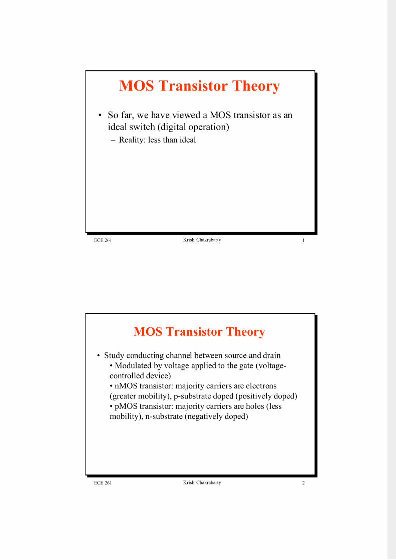
MOS Transistor Theory
• So far, we have viewed a MOS transistor as an
ideal switch (digital operation)
– Reality: less than ideal
ECE 261 Krish Chakrabarty 2
MOS Transistor Theory
• Study conducting channel between source and drain
• Modulated by voltage applied to the gate (voltage-
controlled device)
• nMOS transistor: majority carriers are electrons
(greater mobility), p-substrate doped (positively doped)
• pMOS transistor: majority carriers are holes (less
mobility), n-substrate (negatively doped)

7/27/2019 MOS Theory
http://slidepdf.com/reader/full/mos-theory 2/8
ECE 261 Krish Chakrabarty 3
Gate Biasing
p-substrate
n+ n+
Source
Gate
Drain
Channel
+ -
E
SiO2
VSS (Gnd)
• Vgs=0: no current flows from
source to drain (insulated by
two reverse biased pn
junctions
• Vgs>0: electric field created
across substrate
• Electrons accumulate under gate: region changes from p-type
to n-type• Conduction path between source and drain
ECE 261 Krish Chakrabarty 4
nMOS Device Behavior
Vgs << Vt
Polysilicon gate p-substrate
Accumulation
mode
• Enhancement-mode transistor: Conducts when gate bias
Vgs > Vt
• Depletion-mode transistor: Conducts when gate bias is zero
Vgs = Vt
Depletion mode
Depletion region
Oxide insulator
Vgs > Vt
Inversion mode
Depletion region
Inversion
Region
(n-type)

7/27/2019 MOS Theory
http://slidepdf.com/reader/full/mos-theory 3/8
ECE 261 Krish Chakrabarty 5
Transistor Operating Regions
• Cut-off region: accumulation mode, zero current flow
• Linear region: Vds <= Vgs-Vt, weak inversion layer,
drain current depends on Vgs and Vds
• Saturated region: Vds > Vgs-Vt, strong inversion
layer, drain current independent of Vds
ECE 261 Krish Chakrabarty 6
Threshold Voltage: Concept
n+n+
p-substrate
D S
G
B
VGS
+
-
Depletion
Region
n-channel

7/27/2019 MOS Theory
http://slidepdf.com/reader/full/mos-theory 4/8
ECE 261 Krish Chakrabarty 7
Current-Voltage Relations
n+n+
p-substrate
D
S
G
B
V GS
x L
V ( x )
+ –
V DS
I D
MOS transistor and its bias conditions
ECE 261 Krish Chakrabarty 8
Current-Voltage Relations

7/27/2019 MOS Theory
http://slidepdf.com/reader/full/mos-theory 5/8
ECE 261 Krish Chakrabarty 9
Current-Voltage Relations
k n: transconductance of transistor
W : width-to-length ratio
L
• As W increases, more carriers available to conduct current
• As L increases, Vds diminishes in effect (more voltage
drop). Takes longer to push carriers across the transistor,
reducing current flow
ECE 261 Krish Chakrabarty 10
Typical Parameter Values
k Vt
n-type 24 microA/V2 0.8V
p-type 9 microA/V2 -0.8V
Why is k higher for n-type transistors?

7/27/2019 MOS Theory
http://slidepdf.com/reader/full/mos-theory 6/8
ECE 261 Krish Chakrabarty 11
Transistor in Saturation
n+n+
S
G
VGS
D
VDS > VGS - VT
VGS - VT
+-
Channel is pinched off
ECE 261 Krish Chakrabarty 12
The Gate Capacitance

7/27/2019 MOS Theory
http://slidepdf.com/reader/full/mos-theory 7/8
ECE 261 Krish Chakrabarty 13
Diffusion Capacitance
ECE 261 Krish Chakrabarty 14
Parasitic Resistances
W
L D
Drain
Draincontact
Polysilicon gate
D S
G
RS R D
V GS,eff
R S = (LS/W)R + R C
R D = (LD/W)R + R C
R C: contact resistance
R : sheet resistance per square
of drain-source diffusion

7/27/2019 MOS Theory
http://slidepdf.com/reader/full/mos-theory 8/8
ECE 261 Krish Chakrabarty 15
Body Effect
• Many MOS devices on a common substrate
– Substrate voltage of all devices are normally equal
• But several devices may be connected in series
– Increase in source-to-substrate voltage as we proceed vertically
along the chain
d1
d2
s1
s2
V12
V11
g1
g2
Vsb1 = 0
Vsb2 = 0• Net effect: slight increase
in threshold voltage Vt,
Vt2>Vt1