Embed Size (px)
Citation preview
MOSFETMetalOxideSemiconductorFieldEffectTransistor
CoolMOS™P6600VCoolMOS™P6PowerTransistorIPx60R125P6
DataSheetRev.2.0Final
PowerManagement&Multimarket
2
600VCoolMOS™P6PowerTransistor
IPW60R125P6,IPP60R125P6,IPA60R125P6
Rev.2.0,2014-03-07Final Data Sheet
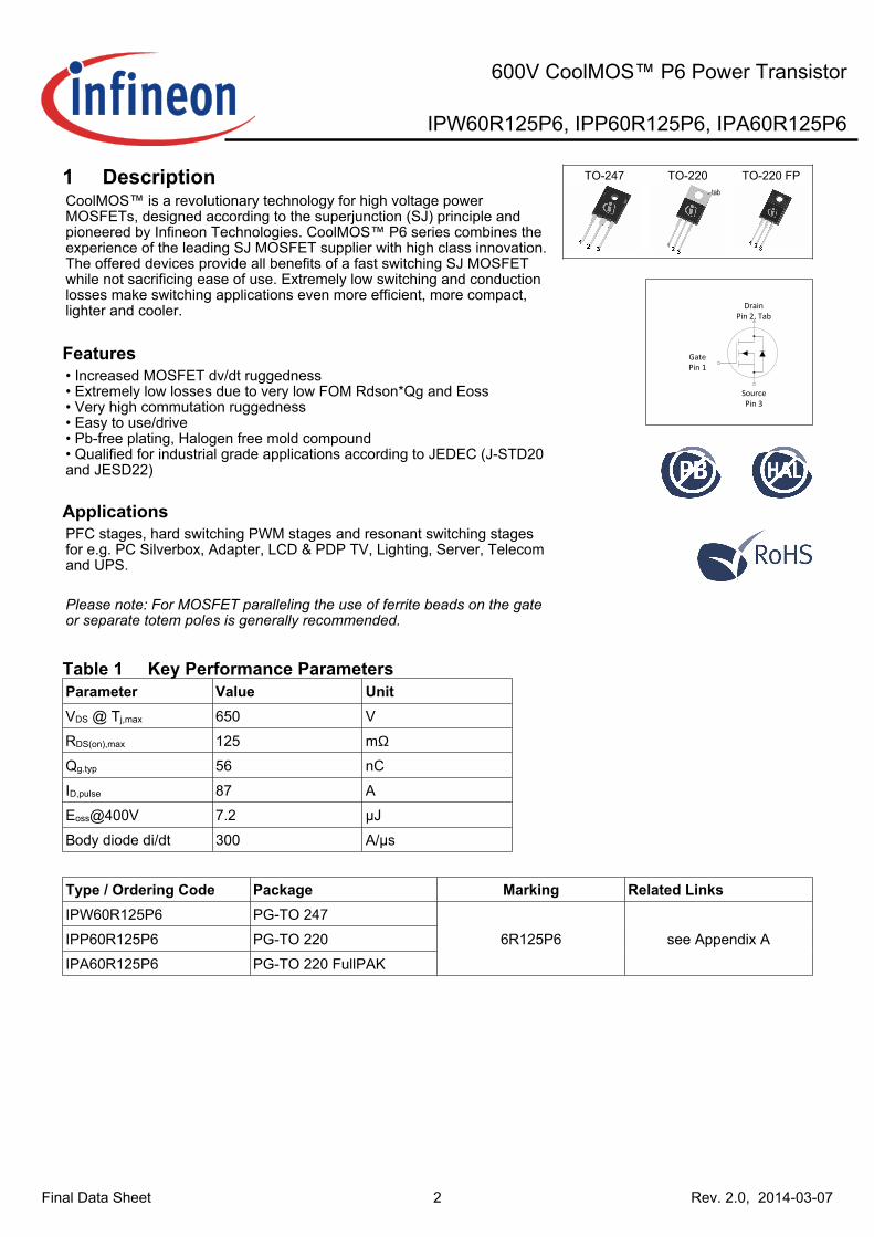
TO-247tab
TO-220 TO-220FP
DrainPin 2, Tab
GatePin 1
SourcePin 3
1DescriptionCoolMOS™isarevolutionarytechnologyforhighvoltagepowerMOSFETs,designedaccordingtothesuperjunction(SJ)principleandpioneeredbyInfineonTechnologies.CoolMOS™P6seriescombinestheexperienceoftheleadingSJMOSFETsupplierwithhighclassinnovation.TheoffereddevicesprovideallbenefitsofafastswitchingSJMOSFETwhilenotsacrificingeaseofuse.Extremelylowswitchingandconductionlossesmakeswitchingapplicationsevenmoreefficient,morecompact,lighterandcooler.
Features•IncreasedMOSFETdv/dtruggedness•ExtremelylowlossesduetoverylowFOMRdson*QgandEoss•Veryhighcommutationruggedness•Easytouse/drive•Pb-freeplating,Halogenfreemoldcompound•QualifiedforindustrialgradeapplicationsaccordingtoJEDEC(J-STD20andJESD22)
ApplicationsPFCstages,hardswitchingPWMstagesandresonantswitchingstagesfore.g.PCSilverbox,Adapter,LCD&PDPTV,Lighting,Server,TelecomandUPS.
Pleasenote:ForMOSFETparallelingtheuseofferritebeadsonthegateorseparatetotempolesisgenerallyrecommended.
Table1KeyPerformanceParametersParameter Value UnitVDS @ Tj,max 650 V
RDS(on),max 125 mΩ
Qg.typ 56 nC
ID,pulse 87 A
Eoss@400V 7.2 µJ
Body diode di/dt 300 A/µs
Type/OrderingCode Package Marking RelatedLinksIPW60R125P6 PG-TO 247
IPP60R125P6 PG-TO 220
IPA60R125P6 PG-TO 220 FullPAK
6R125P6 see Appendix A
3
600VCoolMOS™P6PowerTransistor
IPW60R125P6,IPP60R125P6,IPA60R125P6
Rev.2.0,2014-03-07Final Data Sheet
TableofContentsDescription . . . . . . . . . . . . . . . . . . . . . . . . . . . . . . . . . . . . . . . . . . . . . . . . . . . . . . . . . . . . . . . . . . . . . . . . . . . . . 2
Maximum ratings . . . . . . . . . . . . . . . . . . . . . . . . . . . . . . . . . . . . . . . . . . . . . . . . . . . . . . . . . . . . . . . . . . . . . . . . 4
Thermal characteristics . . . . . . . . . . . . . . . . . . . . . . . . . . . . . . . . . . . . . . . . . . . . . . . . . . . . . . . . . . . . . . . . . . . . 5
Electrical characteristics . . . . . . . . . . . . . . . . . . . . . . . . . . . . . . . . . . . . . . . . . . . . . . . . . . . . . . . . . . . . . . . . . . . 6
Electrical characteristics diagrams . . . . . . . . . . . . . . . . . . . . . . . . . . . . . . . . . . . . . . . . . . . . . . . . . . . . . . . . . . . 8
Test Circuits . . . . . . . . . . . . . . . . . . . . . . . . . . . . . . . . . . . . . . . . . . . . . . . . . . . . . . . . . . . . . . . . . . . . . . . . . . . 13
Package Outlines . . . . . . . . . . . . . . . . . . . . . . . . . . . . . . . . . . . . . . . . . . . . . . . . . . . . . . . . . . . . . . . . . . . . . . . 14
Appendix A . . . . . . . . . . . . . . . . . . . . . . . . . . . . . . . . . . . . . . . . . . . . . . . . . . . . . . . . . . . . . . . . . . . . . . . . . . . . 17
Revision History . . . . . . . . . . . . . . . . . . . . . . . . . . . . . . . . . . . . . . . . . . . . . . . . . . . . . . . . . . . . . . . . . . . . . . . . 18
Disclaimer . . . . . . . . . . . . . . . . . . . . . . . . . . . . . . . . . . . . . . . . . . . . . . . . . . . . . . . . . . . . . . . . . . . . . . . . . . . . 18
4
600VCoolMOS™P6PowerTransistor
IPW60R125P6,IPP60R125P6,IPA60R125P6
Rev.2.0,2014-03-07Final Data Sheet
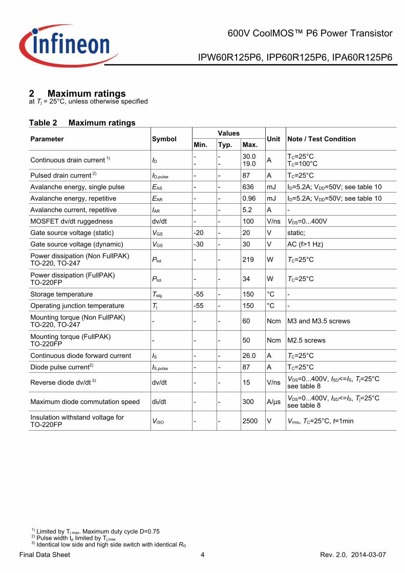
2MaximumratingsatTj=25°C,unlessotherwisespecified
Table2MaximumratingsValues
Min. Typ. Max.Parameter Symbol Unit Note/TestCondition
Continuous drain current 1) ID --
--
30.019.0 A TC=25°C
TC=100°C
Pulsed drain current 2) ID,pulse - - 87 A TC=25°C
Avalanche energy, single pulse EAS - - 636 mJ ID=5.2A; VDD=50V; see table 10
Avalanche energy, repetitive EAR - - 0.96 mJ ID=5.2A; VDD=50V; see table 10
Avalanche current, repetitive IAR - - 5.2 A -
MOSFET dv/dt ruggedness dv/dt - - 100 V/ns VDS=0...400V
Gate source voltage (static) VGS -20 - 20 V static;
Gate source voltage (dynamic) VGS -30 - 30 V AC (f>1 Hz)
Power dissipation (Non FullPAK) TO-220, TO-247 Ptot - - 219 W TC=25°C
Power dissipation (FullPAK) TO-220FP Ptot - - 34 W TC=25°C
Storage temperature Tstg -55 - 150 °C -
Operating junction temperature Tj -55 - 150 °C -
Mounting torque (Non FullPAK) TO-220, TO-247 - - - 60 Ncm M3 and M3.5 screws
Mounting torque (FullPAK) TO-220FP - - - 50 Ncm M2.5 screws
Continuous diode forward current IS - - 26.0 A TC=25°C
Diode pulse current2) IS,pulse - - 87 A TC=25°C
Reverse diode dv/dt 3) dv/dt - - 15 V/ns VDS=0...400V,ISD<=IS,Tj=25°Csee table 8
Maximum diode commutation speed dif/dt - - 300 A/µs VDS=0...400V,ISD<=IS,Tj=25°Csee table 8
Insulation withstand voltage forTO-220FP VISO - - 2500 V Vrms,TC=25°C,t=1min
1) Limited by Tj max. Maximum duty cycle D=0.75 2) Pulse width tp limited by Tj,max3)IdenticallowsideandhighsideswitchwithidenticalRG
5
600VCoolMOS™P6PowerTransistor
IPW60R125P6,IPP60R125P6,IPA60R125P6
Rev.2.0,2014-03-07Final Data Sheet
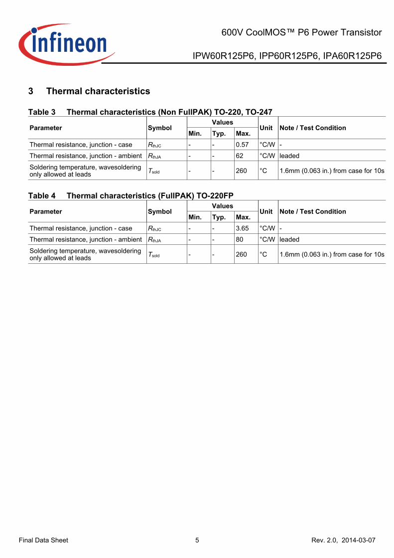
3Thermalcharacteristics
Table3Thermalcharacteristics(NonFullPAK)TO-220,TO-247Values
Min. Typ. Max.Parameter Symbol Unit Note/TestCondition
Thermal resistance, junction - case RthJC - - 0.57 °C/W -
Thermal resistance, junction - ambient RthJA - - 62 °C/W leaded
Soldering temperature, wavesolderingonly allowed at leads Tsold - - 260 °C 1.6mm (0.063 in.) from case for 10s
Table4Thermalcharacteristics(FullPAK)TO-220FPValues
Min. Typ. Max.Parameter Symbol Unit Note/TestCondition
Thermal resistance, junction - case RthJC - - 3.65 °C/W -
Thermal resistance, junction - ambient RthJA - - 80 °C/W leaded
Soldering temperature, wavesolderingonly allowed at leads Tsold - - 260 °C 1.6mm (0.063 in.) from case for 10s
6
600VCoolMOS™P6PowerTransistor
IPW60R125P6,IPP60R125P6,IPA60R125P6
Rev.2.0,2014-03-07Final Data Sheet
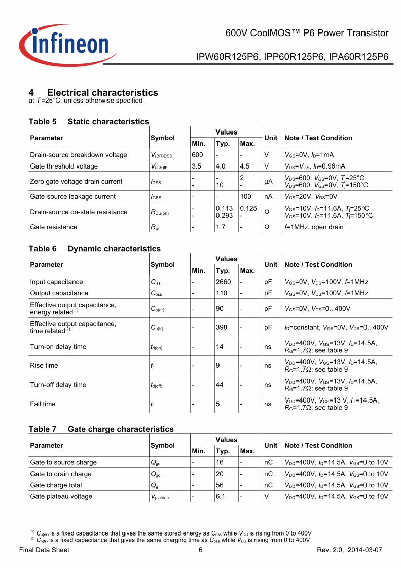
4ElectricalcharacteristicsatTj=25°C,unlessotherwisespecified
Table5StaticcharacteristicsValues
Min. Typ. Max.Parameter Symbol Unit Note/TestCondition
Drain-source breakdown voltage V(BR)DSS 600 - - V VGS=0V,ID=1mA
Gate threshold voltage V(GS)th 3.5 4.0 4.5 V VDS=VGS,ID=0.96mA
Zero gate voltage drain current IDSS --
-10
2- µA VDS=600,VGS=0V,Tj=25°C
VDS=600,VGS=0V,Tj=150°C
Gate-source leakage current IGSS - - 100 nA VGS=20V,VDS=0V
Drain-source on-state resistance RDS(on)--
0.1130.293
0.125- Ω VGS=10V,ID=11.6A,Tj=25°C
VGS=10V,ID=11.6A,Tj=150°C
Gate resistance RG - 1.7 - Ω f=1MHz,opendrain
Table6DynamiccharacteristicsValues
Min. Typ. Max.Parameter Symbol Unit Note/TestCondition
Input capacitance Ciss - 2660 - pF VGS=0V,VDS=100V,f=1MHz
Output capacitance Coss - 110 - pF VGS=0V,VDS=100V,f=1MHz
Effective output capacitance, energy related 1) Co(er) - 90 - pF VGS=0V,VDS=0...400V
Effective output capacitance, time related 2) Co(tr) - 398 - pF ID=constant,VGS=0V,VDS=0...400V
Turn-on delay time td(on) - 14 - ns VDD=400V,VGS=13V,ID=14.5A,RG=1.7Ω;seetable9
Rise time tr - 9 - ns VDD=400V,VGS=13V,ID=14.5A,RG=1.7Ω;seetable9
Turn-off delay time td(off) - 44 - ns VDD=400V,VGS=13V,ID=14.5A,RG=1.7Ω;seetable9
Fall time tf - 5 - ns VDD=400V,VGS=13V,ID=14.5A,RG=1.7Ω;seetable9
Table7GatechargecharacteristicsValues
Min. Typ. Max.Parameter Symbol Unit Note/TestCondition
Gate to source charge Qgs - 16 - nC VDD=400V,ID=14.5A,VGS=0to10V
Gate to drain charge Qgd - 20 - nC VDD=400V,ID=14.5A,VGS=0to10V
Gate charge total Qg - 56 - nC VDD=400V,ID=14.5A,VGS=0to10V
Gate plateau voltage Vplateau - 6.1 - V VDD=400V,ID=14.5A,VGS=0to10V
1)Co(er)isafixedcapacitancethatgivesthesamestoredenergyasCosswhileVDSisrisingfrom0to400V2)Co(tr)isafixedcapacitancethatgivesthesamechargingtimeasCosswhileVDSisrisingfrom0to400V
7
600VCoolMOS™P6PowerTransistor
IPW60R125P6,IPP60R125P6,IPA60R125P6
Rev.2.0,2014-03-07Final Data Sheet
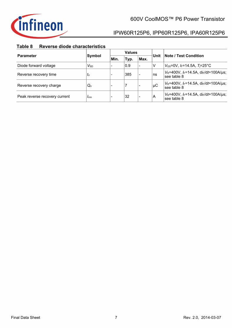
Table8ReversediodecharacteristicsValues
Min. Typ. Max.Parameter Symbol Unit Note/TestCondition
Diode forward voltage VSD - 0.9 - V VGS=0V,IF=14.5A,Tj=25°C
Reverse recovery time trr - 385 - ns VR=400V,IF=14.5A,diF/dt=100A/µs;see table 8
Reverse recovery charge Qrr - 7 - µC VR=400V,IF=14.5A,diF/dt=100A/µs;see table 8
Peak reverse recovery current Irrm - 32 - A VR=400V,IF=14.5A,diF/dt=100A/µs;see table 8

8
600VCoolMOS™P6PowerTransistor
IPW60R125P6,IPP60R125P6,IPA60R125P6
Rev.2.0,2014-03-07Final Data Sheet
5Electricalcharacteristicsdiagrams
Diagram1:Powerdissipation(NonFullPAK)
TC[°C]
Ptot[W
]
0 25 50 75 100 125 1500
50
100
150
200
250
Ptot=f(TC)
Diagram2:Powerdissipation(FullPAK)
TC[°C]
Ptot[W
]
0 25 50 75 100 125 1500
5
10
15
20
25
30
35
40
Ptot=f(TC)
Diagram3:Max.transientthermalimpedance(NonFullPAK)
tp[s]
ZthJC[K
/W]
10-5 10-4 10-3 10-2 10-110-2
10-1
100
101
0.5
0.2
0.1
0.05
0.02
0.01
single pulse
ZthJC=f(tP);parameter:D=tp/T
Diagram4:Max.transientthermalimpedance(FullPAK)
tp[s]
ZthJC[K
/W]
10-5 10-4 10-3 10-2 10-1 100 10110-2
10-1
100
101
0.5
0.2
0.1
0.05
0.02
0.01
single pulse
ZthJC=f(tP);parameter:D=tp/T
9
600VCoolMOS™P6PowerTransistor
IPW60R125P6,IPP60R125P6,IPA60R125P6
Rev.2.0,2014-03-07Final Data Sheet
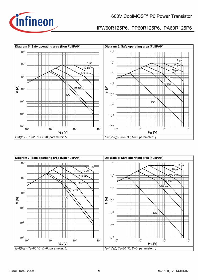
Diagram5:Safeoperatingarea(NonFullPAK)
VDS[V]
ID[A
]
100 101 102 10310-3
10-2
10-1
100
101
102
103
1 µs
10 µs
100 µs
1 ms
10 ms
DC
ID=f(VDS);TC=25°C;D=0;parameter:tp
Diagram6:Safeoperatingarea(FullPAK)
VDS[V]
ID[A
]
100 101 102 10310-4
10-3
10-2
10-1
100
101
102
103
1 µs
10 µs
100 µs
1 ms
10 ms
DC
ID=f(VDS);TC=25°C;D=0;parameter:tp
Diagram7:Safeoperatingarea(NonFullPAK)
VDS[V]
ID[A
]
100 101 102 10310-3
10-2
10-1
100
101
102
1 µs
10 µs
100 µs
1 ms
10 ms
DC
ID=f(VDS);TC=80°C;D=0;parameter:tp
Diagram8:Safeoperatingarea(FullPAK)
VDS[V]
ID[A
]
100 101 102 10310-4
10-3
10-2
10-1
100
101
1021 µs
10 µs
100 µs
1 ms
10 ms
DC
ID=f(VDS);TC=80°C;D=0;parameter:tp
10
600VCoolMOS™P6PowerTransistor
IPW60R125P6,IPP60R125P6,IPA60R125P6
Rev.2.0,2014-03-07Final Data Sheet
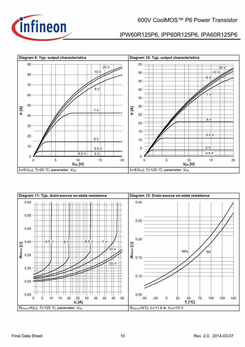
Diagram9:Typ.outputcharacteristics
VDS[V]
ID[A
]
0 5 10 15 200
10
20
30
40
50
60
70
80
9020 V
10 V
8 V
7 V
6 V
5.5 V
5 V4.5 V
ID=f(VDS);Tj=25°C;parameter:VGS
Diagram10:Typ.outputcharacteristics
VDS[V]
ID[A
]
0 5 10 15 200
5
10
15
20
25
30
35
40
45
50
5520 V
10 V
8 V
7 V
6 V
5.5 V
5 V
4.5 V
ID=f(VDS);Tj=125°C;parameter:VGS
Diagram11:Typ.drain-sourceon-stateresistance
ID[A]
RDS(on
) [Ω]
0 5 10 15 20 25 30 35 40 45 500.20
0.25
0.30
0.35
0.40
0.45
0.50
0.55
20 V
5.5 V 6 V 6.5 V 7 V
10 V
RDS(on)=f(ID);Tj=125°C;parameter:VGS
Diagram12:Drain-sourceon-stateresistance
Tj[°C]
RDS(on
) [Ω]
-50 -25 0 25 50 75 100 125 1500.05
0.10
0.15
0.20
0.25
0.30
98% typ
RDS(on)=f(Tj);ID=11.6A;VGS=10V
11
600VCoolMOS™P6PowerTransistor
IPW60R125P6,IPP60R125P6,IPA60R125P6
Rev.2.0,2014-03-07Final Data Sheet
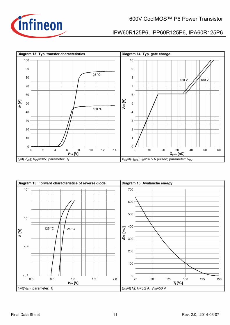
Diagram13:Typ.transfercharacteristics
VGS[V]
ID[A
]
0 2 4 6 8 10 12 140
10
20
30
40
50
60
70
80
90
100
25 °C
150 °C
ID=f(VGS);VDS=20V;parameter:Tj
Diagram14:Typ.gatecharge
Qgate[nC]
VGS [V]
0 10 20 30 40 50 600
1
2
3
4
5
6
7
8
9
10
480 V120 V
VGS=f(Qgate);ID=14.5Apulsed;parameter:VDD
Diagram15:Forwardcharacteristicsofreversediode
VSD[V]
IF [A]
0.0 0.5 1.0 1.5 2.010-1
100
101
102
125 °C 25 °C
IF=f(VSD);parameter:Tj
Diagram16:Avalancheenergy
Tj[°C]
EAS [mJ]
25 50 75 100 125 1500
100
200
300
400
500
600
700
EAS=f(Tj);ID=5.2A;VDD=50V

12
600VCoolMOS™P6PowerTransistor
IPW60R125P6,IPP60R125P6,IPA60R125P6
Rev.2.0,2014-03-07Final Data Sheet
Diagram17:Drain-sourcebreakdownvoltage
Tj[°C]
VBR(DSS
) [V]
-75 -50 -25 0 25 50 75 100 125 150 175520
540
560
580
600
620
640
660
680
700
VBR(DSS)=f(Tj);ID=1mA
Diagram18:Typ.capacitances
VDS[V]
C[p
F]
0 100 200 300 400 500100
101
102
103
104
Ciss
Coss
Crss
C=f(VDS);VGS=0V;f=1MHz
Diagram19:Typ.Cossstoredenergy
VDS[V]
Eoss[µ
J]
0 100 200 300 400 5000
1
2
3
4
5
6
7
8
9
10
Eoss=f(VDS)
13
600VCoolMOS™P6PowerTransistor
IPW60R125P6,IPP60R125P6,IPA60R125P6
Rev.2.0,2014-03-07Final Data Sheet
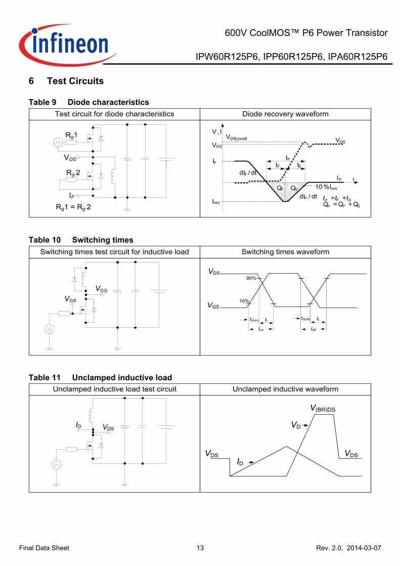
6TestCircuits
Table9DiodecharacteristicsTest circuit for diode characteristics Diode recovery waveform
t
V ,I
Irrm
IF
VDS
10 %Irrm
trrtF tS
QF QS
dIF / dt
dIrr / dt
VDS(peak)
Qrr = QF +QS
trr =tF +tS
VDS
IF
VDS
IF
Rg1
Rg 2
Rg1 = Rg 2
Table10SwitchingtimesSwitching times test circuit for inductive load Switching times waveform
VDS
VGS
td(on) td(off)tr
ton
tf
toff
10%
90%
VDS
VGS
Table11UnclampedinductiveloadUnclamped inductive load test circuit Unclamped inductive waveform
VDS
VD
V(BR)DS
IDVDS
VDSID

14
600VCoolMOS™P6PowerTransistor
IPW60R125P6,IPP60R125P6,IPA60R125P6
Rev.2.0,2014-03-07Final Data Sheet
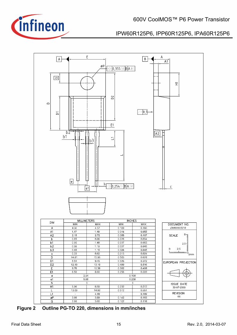
7PackageOutlines
Figure1OutlinePG-TO247,dimensionsinmm/inches
15
600VCoolMOS™P6PowerTransistor
IPW60R125P6,IPP60R125P6,IPA60R125P6
Rev.2.0,2014-03-07Final Data Sheet
Figure2OutlinePG-TO220,dimensionsinmm/inches
16
600VCoolMOS™P6PowerTransistor
IPW60R125P6,IPP60R125P6,IPA60R125P6
Rev.2.0,2014-03-07Final Data Sheet
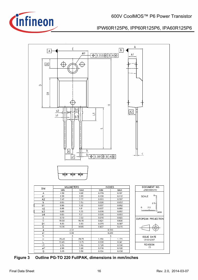
Figure3OutlinePG-TO220FullPAK,dimensionsinmm/inches

17
600VCoolMOS™P6PowerTransistor
IPW60R125P6,IPP60R125P6,IPA60R125P6
Rev.2.0,2014-03-07Final Data Sheet
8AppendixA
Table12RelatedLinks
• IFXCoolMOSTMP6Webpage:www.infineon.com
• IFXCoolMOSTMP6applicationnote:www.infineon.com
• IFXCoolMOSTMP6simulationmodel:www.infineon.com
• IFXDesigntools:www.infineon.com

18
600VCoolMOS™P6PowerTransistor
IPW60R125P6,IPP60R125P6,IPA60R125P6
Rev.2.0,2014-03-07Final Data Sheet
RevisionHistoryIPW60R125P6, IPP60R125P6, IPA60R125P6
Revision:2014-03-07,Rev.2.0
Previous Revision
Revision Date Subjects (major changes since last revision)
2.0 2014-03-07 Release of final version
WeListentoYourCommentsAnyinformationwithinthisdocumentthatyoufeeliswrong,unclearormissingatall?Yourfeedbackwillhelpustocontinuouslyimprovethequalityofthisdocument.Pleasesendyourproposal(includingareferencetothisdocument)to:[email protected]
PublishedbyInfineonTechnologiesAG81726München,Germany©2014InfineonTechnologiesAGAllRightsReserved.
LegalDisclaimerTheinformationgiveninthisdocumentshallinnoeventberegardedasaguaranteeofconditionsorcharacteristics.Withrespecttoanyexamplesorhintsgivenherein,anytypicalvaluesstatedhereinand/oranyinformationregardingtheapplicationofthedevice,InfineonTechnologiesherebydisclaimsanyandallwarrantiesandliabilitiesofanykind,includingwithoutlimitation,warrantiesofnon-infringementofintellectualpropertyrightsofanythirdparty.
InformationForfurtherinformationontechnology,deliverytermsandconditionsandpricespleasecontactyournearestInfineonTechnologiesOffice(www.infineon.com).
WarningsDuetotechnicalrequirements,componentsmaycontaindangeroussubstances.Forinformationonthetypesinquestion,pleasecontactthenearestInfineonTechnologiesOffice.TheInfineonTechnologiescomponentdescribedinthisDataSheetmaybeusedinlife-supportdevicesorsystemsand/orautomotive,aviationandaerospaceapplicationsorsystemsonlywiththeexpresswrittenapprovalofInfineonTechnologies,ifafailureofsuchcomponentscanreasonablybeexpectedtocausethefailureofthatlife-support,automotive,aviationandaerospacedeviceorsystemortoaffectthesafetyoreffectivenessofthatdeviceorsystem.Lifesupportdevicesorsystemsareintendedtobeimplantedinthehumanbodyortosupportand/ormaintainandsustainand/orprotecthumanlife.Iftheyfail,itisreasonabletoassumethatthehealthoftheuserorotherpersonsmaybeendangered.