Embed Size (px)
Citation preview

MPC5744PMPC5744P Data Sheet32-bit MCU suitable for ISO26262 ASIL-D chassis and safety applicationsFeatures
• The MPC5744P microcontroller is based on the PowerArchitecture® developed by Freescale. It targetschassis and safety applications and other applicationsrequiring a high Automotive Safety Integrity Level(ASIL). The MPC5744P is a SafeAssure solution.
• This document provides electrical specifications, pinassignments, and package diagram information for theMPC5744P series of microcontroller units (MCUs).For functional characteristics and the programmingmodel, see the MPC5744P Reference Manual.
• Junction temperature: The upper limit is 150°C or165°C depending on the device marking.
Freescale Semiconductor Document Number MPC5744P
Data Sheet: Technical Data Rev. 5, 08/2015
© 2011–2015 Freescale Semiconductor, Inc.
NXP reserves the right to change the detail specifications as may be required to permit improvements in the design of its products.

Table of Contents1 Introduction...............................................................................3
1.1 Features..........................................................................3
1.2 Block Diagram.................................................................5
2 Pinouts......................................................................................6
2.1 Package pinouts and ballmap.........................................6
2.2 Pin/ball descriptions .......................................................8
2.2.1 Pin/ball startup and reset states.......................8
2.2.2 Power supply and reference voltage pins/balls 9
2.2.3 System pins/balls..............................................13
2.2.4 LVDS pins/balls................................................14
2.2.5 Generic pins/balls.............................................15
2.2.6 Peripheral input muxing....................................48
3 Electrical characteristics............................................................60
3.1 Introduction......................................................................60
3.2 165°C junction temperature option..................................60
3.3 Absolute maximum ratings..............................................61
3.4 Recommended operating conditions...............................62
3.5 Thermal characteristics...................................................63
3.5.1 General notes for specifications at maximum
junction temperature.........................................64
3.6 Electromagnetic compatibility (EMC)..............................66
3.7 Electrostatic discharge (ESD) characteristics.................67
3.8 Voltage regulator electrical characteristics......................67
3.9 DC electrical characteristics............................................70
3.10 Supply current characteristics.........................................72
3.11 Temperature sensor........................................................74
3.12 Main oscillator electrical characteristics..........................75
3.13 PLLDIG electrical characteristics....................................77
3.14 16 MHz Internal RC Oscillator (IRCOSC) electrical
specifications...................................................................78
3.15 ADC electrical characteristics..........................................79
3.16 Flash memory specifications...........................................82
3.16.1 Maximum junction temperature 150°C.............82
3.16.2 Maximum junction temperature 165°C.............85
3.16.3 Flash memory read wait-state and address-
pipeline control settings....................................89
3.17 SGEN electrical characteristics.......................................90
3.18 RESET sequence duration..............................................90
3.19 AC specifications.............................................................91
3.19.1 Reset pad (EXT_POR, RESET) electrical
characteristics...................................................91
3.19.2 WKUP/NMI timing.............................................93
3.19.3 Debug/JTAG/Nexus/Aurora timing...................93
3.19.4 External interrupt timing (IRQ pin)....................101
3.19.5 SPI timing.........................................................102
3.19.6 LFAST..............................................................107
3.19.7 FlexRay............................................................111
3.19.8 Ethernet switching specifications......................114
4 Obtaining package dimensions.................................................116
5 Ordering information.................................................................117
6 Document revision history.........................................................118
MPC5744P Data Sheet Data Sheet, Rev. 5, 08/2015.
2 Freescale Semiconductor, Inc.

Introduction
1.1 FeaturesThe following table summarizes the features of the MPC5744P.
Table 1. MPC5744P feature summary
Feature Details
CPU
Power Architecture 2 x e200z4 in delayed lock step
Architecture Harvard
Execution speed 0 MHz to 200 MHz (+2% FM)
Embedded FPU Yes
Core MPU 24 regions
Instruction Set PPC No
Instruction Set VLE Yes
Instruction cache 8 KB, EDC
Data cache 4 KB, EDC
Data local memory 64 KB, ECC
System MPU Yes (16 regions)
Buses
Core bus AHB, 32-bit address, 64-bit data, e2e ECC
Internal periphery bus 32-bit address, 32-bit data
Crossbar
Master x slave ports 4 x 5
Memory—see Table 2 for additional details
Code/data flash memory 2.5 MB, ECC, RWW
Data flash memory Supported with RWW
SRAM 384 KB, ECC
Overlay access to SRAM from Flash Memory Controller Yes
Modules
Interrupt controller 32 interrupt priority levels, 16 SW programmable interrupts
PIT 1 module with 4 channels
System Timer Module (STM) 1 module with 4 channels
Software Watchdog Timer (SWT) Yes
eDMA 32 channels, in delayed lock step
FlexRay 1 module with 64 message buffer, dual channel
FlexCAN 3 modules with 64 message buffer
LINFlexD (UART and LIN with DMA support) 2 modules
Table continues on the next page...
1
Introduction
MPC5744P Data Sheet Data Sheet, Rev. 5, 08/2015.
Freescale Semiconductor, Inc. 3

Table 1. MPC5744P feature summary (continued)
Feature Details
Clockout Yes
Fault Control and Collection Unit (FCCU) Yes
Cross Triggering Unit (CTU) 2 modules
eTimer 3 modules with 6 channels
FlexPWM 2 modules with 4 x (2+1) channels
Analog-to-digital converter (ADC) 4 modules with 12-bit ADC, each with 16 channels (25external channels including shared channels plus internalchannels)
Sine-wave generator (SGEN) 32 point
SPI 4 modules
As many as 8 chip selects
CRC Unit Yes
SENT 2 modules with 2 channels
Interprocessor serial link interface (SIPI) Yes
Junction temperature sensor Yes (replicated module)
Digital I/Os ≥ 16
Peripheral register protection Yes
Ethernet Yes
Error Injection Module (EIM) Yes
Supply
Device Power Supply 3.3 V with external ballast transistor
3.3 V with external 1.25 V low drop-out (LDO) regulator
ADC Analog Reference voltage 3.15 V to 5.5 V
Clocking
Phase Lock Loop (PLL) 1 x PLL and 1 coupled FMPLL
Internal RC Oscillator 16 MHz
External Crystal Oscillator 8 MHz to 40 MHz
Low power modes
HALT and STOP Yes
Debug
Nexus Level 3+, MDO and Aurora interface
Package
LQFP 144 pins, 0.5 mm pitch, 20 mm x 20 mm outline
MAPBGA 257 MAPBGA, 0.8 mm pitch, 14 mm x 14 mm outline
Temperature
Temperature range (junction) -40°C to +150°C, option for 165°C
Ambient temperature range (LQFP) -40°C to +125°C, 135°C option (with 165°C junction option)
Ambient temperature range (BGA) -40°C to +125°C, 135°C option (with 165°C junction option)
Introduction
MPC5744P Data Sheet Data Sheet, Rev. 5, 08/2015.
4 Freescale Semiconductor, Inc.

Table 2. Flash memory and SRAM sizes of MPC5744P, MPC5743P, MPC5742P, andMPC5741P
Part number Flash memory SRAM
MPC5744P 2.5 MB 384 KB
MPC5743P 2.0 MB 256 KB
MPC5742P 1.5 MB 192 KB
MPC5741P 1.0 MB 128 KB
1.2 Block Diagram
The following figure is a top-level diagram that shows the functional organization of thesystem.
Figure 1. System Block Diagram
Introduction
MPC5744P Data Sheet Data Sheet, Rev. 5, 08/2015.
Freescale Semiconductor, Inc. 5

Pinouts
2.1 Package pinouts and ballmap
The following figures show the LQFP pinout and the BGA ballmap.
Figure 2. 144LQFP pinout
2
Pinouts
MPC5744P Data Sheet Data Sheet, Rev. 5, 08/2015.
6 Freescale Semiconductor, Inc.

Figure 3. 257MAPBGA ballmap
Pinouts
MPC5744P Data Sheet Data Sheet, Rev. 5, 08/2015.
Freescale Semiconductor, Inc. 7

2.2 Pin/ball descriptions
The following sections provide signal descriptions and related information about thefunctionality and configuration of the device. Note that this section is under development.
2.2.1 Pin/ball startup and reset states
The following table provides startup state and reset state information for device pins/balls.
The startup state and subsequent states of the following pins/balls cannot be configuredby the user:
• JCOMP• TMS• TCK• XTAL/EXTAL• FCCU_F[0] and FCCU_F[1]• EXT_POR_B• RESET_B
The user can configure the state after reset of the following pins/balls by programmingthe applicable MSCRs/IMCRs:
• GPIOs• Analog inputs• TDI• TDO• NMI_B• FAB• ABS[0]• ABS[2]
Table 3. Pin/ball startup and reset states
Pin/ball Startup state1 State during reset State after reset 144LQFP 257MAPBGA
GPIOs hi-z hi-z hi-z Note2 Note2
Analog inputs3 hi-z hi-z hi-z Note2 Note2
JCOMP (TRST) hi-z input, weak pull-down input, weak pull-down Note4 Note4
TDI hi-z input, weak pull-up input, weak pull-up Note4 Note4
TDO hi-z output, hi-z output, hi-z Note4 Note4
TMS5 hi-z input, weak pull-up input, weak pull-up Note4 Note4
Table continues on the next page...
Pinouts
MPC5744P Data Sheet Data Sheet, Rev. 5, 08/2015.
8 Freescale Semiconductor, Inc.

Table 3. Pin/ball startup and reset states (continued)
Pin/ball Startup state1 State during reset State after reset 144LQFP 257MAPBGA
TCK5 hi-z input, weak pull-up input, weak pull-up Note4 Note4
XTAL/EXTAL hi-z hi-z hi-z Note4 Note4
FCCU_F[0]5 hi-z input, hi-z output/input, hi-z 38 R2
FCCU_F[1]5 hi-z input, hi-z output/input, hi-z 141 C4
EXT_POR_B hi-z input, weak pull-down input, weak pull-down Note4 Note4
RESET_B hi-z input, weak pull-down input, weak pull-down Note4 Note4
NMI_B hi-z input, weak pull-up input,weak pull-up Note4 Note4
FAB hi-z input, weak pull-down input, weak pull-down Note4 Note4
ABS[2] hi-z input, weak pull-down input, weak pull-down Note4 Note4
ABS[0] hi-z input, weak pull-down input, weak pull-down Note4 Note4
1. Startup state is exited when the core and high-voltage supplies reach minimum levels.2. See Generic pins/balls.3. Not all non-supply or reference pins on the device are explicitly defined in this table.4. See System pins/balls.5. This pin/ball is dedicated to and directly connected to a peripheral module pin.
Pinouts
MPC5744P Data Sheet Data Sheet, Rev. 5, 08/2015.
Freescale Semiconductor, Inc. 9

2.2.2 Power supply and reference voltage pins/ballsTable 4. Power supply and reference voltage pins/balls
Supply Package
Symbol Type Description 144LQFP 257MAPBGA
VDD_LV_COR Power Low voltage power Supply 18
39
70
93
131
135
F6
F7
F8
F9
F10
F11
F12
G6
G12
H6
H12
J6
J12
K6
K12
L6
L12
M6
M7
M8
M9
M10
M11
M12
Table continues on the next page...
Pinouts
MPC5744P Data Sheet Data Sheet, Rev. 5, 08/2015.
10 Freescale Semiconductor, Inc.

Table 4. Power supply and reference voltage pins/balls (continued)
Supply Package
Symbol Type Description 144LQFP 257MAPBGA
VSS_LV_COR Ground Low voltage ground. PLL Ground is also connected to lowvoltage ground for core logic on 144LQFP (pin 35).
17
35
40
71
94
96
132
137
B1
G7
G8
G9
G10
G11
H7
H8
H9
H10
H11
J7
J8
J9
J10
J11
K7
K8
K9
K10
K11
L7
L8
L9
L10
L11
VDD_LV_PLL Power PLL low voltage Supply 36 P4
VSS_LV_PLL Ground PLL low voltage Ground 35 N4
Table continues on the next page...
Pinouts
MPC5744P Data Sheet Data Sheet, Rev. 5, 08/2015.
Freescale Semiconductor, Inc. 11

Table 4. Power supply and reference voltage pins/balls (continued)
Supply Package
Symbol Type Description 144LQFP 257MAPBGA
VDD_HV_IO Power High voltage Power Supply for I/O 6
21
72
91
126
A9
B2
B16
D8
D14
G2
M2
T2
T16
U14
VSS_HV_IO Ground High voltage Ground Supply for I/O 7
22
90
127
A1
A2
A16
A17
B1
B9
B17
C3
C15
D9
H2
N2
R3
R15
T1
T17
U1
U2
U16
U17
VDD_HV_PMU
VDD_HV_PMU_AUX
Power PMU high voltage Supply 72 U14
VDD_HV_OSC Power Power Supply for the oscillator 27 M1
VSS_HV_OSC Ground Ground Supply for the oscillator 28 P1
VDD_HV_FLA Power Power Supply and decoupling pin for flash memory 97 H16
VDD_HV_ADV Power High voltage Supply for ADC, TSENS, SGEN (3.3 V) 58 T10
VSS_HV_ADV Ground High voltage Ground for ADC 59 U9
Table continues on the next page...
Pinouts
MPC5744P Data Sheet Data Sheet, Rev. 5, 08/2015.
12 Freescale Semiconductor, Inc.

Table 4. Power supply and reference voltage pins/balls (continued)
Supply Package
Symbol Type Description 144LQFP 257MAPBGA
VDD_HV_ADRE0 Supply High voltage Supply for digital portion of ADC pads
Voltage reference of ADC/TSENS
High voltage Supply for ADC0 pads and shared pads forADC0/1.
50 R7
VSS_HV_ADRE0 Ground High voltage Ground for digital portion of ADC pads
Voltage reference Ground of ADC/TSENS
High voltage Ground for ADC0 pads and shared pads forADC0/1.
51 T7
VDD_HV_ADRE1 Supply High voltage Supply for digital portion of ADC pads
Voltage reference of ADC/TSENS
High voltage Supply for ADC1 pads, shared pads for ADC1/3,and shared pads for ADC2/3.
56 R9
VSS_HV_ADRE1 Ground High voltage Ground for digital portion of ADC pads
Voltage reference Ground of ADC/TSENS
High voltage Ground for ADC1 pads, shared pads forADC1/3, and shared pads for ADC2/3.
57 T9
VDD_LV_LFAST Supply LFAST PLL low voltage Supply — N16
VSS_LV_LFAST Ground LFAST PLL low voltage Ground — N17
VDD_LV_NEXUS Supply Aurora LVDS Supply — J16
VSS_LV_NEXUS Ground Aurora LVDS Ground — K16
2.2.3 System pins/balls
The following table contains information about system pin functions for the devices.
Table 5. System pins/balls
Symbol Type Description 144LQFP 257MAPBGA
NMI_B Input Non-maskable Interrupt 1 E4
XTAL Input Crystal Oscillator/External Clock Input 29 N1
EXTAL Input Input of the oscillator amplifier circuit 30 R1
RESET_B Input Functional Reset 31 P2
EXT_POR_B Input External Power On Reset 130 D6
VPP_TEST1 Input SoC Test Mode 107 D15
JCOMP Input JTAGC, JTAG Compliance Enable 123 A6
TCK Input JTAGC, Test Clock Input 88 H17
TMS Input JTAGC, Test Mode Select 87 H15
TDO Output JTAGC, Test Data Out 89 G14
Table continues on the next page...
Pinouts
MPC5744P Data Sheet Data Sheet, Rev. 5, 08/2015.
Freescale Semiconductor, Inc. 13

Table 5. System pins/balls (continued)
Symbol Type Description 144LQFP 257MAPBGA
TDI Input JTAGC, Test Data Input 86 J17
MDO[0] Output NEXUS, Message data out pins; reflects the state ofthe internal power on reset signal until RESET isnegated
9 G1
MDO[3:1] Output NEXUS, Message data out pins 4,5,8 E1, F1, E2
EVTO Output NEXUS, Event Out Pin 24 K2
EVTI Input NEXUS, Event In Pin 25 L2
MCKO Output NEXUS, Message clock out pin 19 J4
MSEO[1:0] Output NEXUS, Message Start/End out pin 20, 23 J3, K3
RDY_B Output NEXUS, Read/Write Transfer completed — J2
16 K1
BCTRL Output Base control signal of external npn ballast 69 R13
J[11], J[10] -- FSL Factory Test2 — L17, K17
1. VPP_TEST must be connected to ground.2. Do not connect on the board.
2.2.4 LVDS pins/balls
The following tables contain information on LVDS pin functions for the devices.
Table 6. SIPI LFAST LVDS pin descriptions
Functionalblock
Port pin Signal Signal description Direction 257MAPBGA
SIPI LFAST1, 2 I[5] SIPI_TXN Interprocessor Bus LFAST, LVDS TransmitNegative Terminal
O N15
C[12]3 SIPI_TXP Interprocessor Bus LFAST, LVDS TransmitPositive Terminal
O M14
I[6] SIPI_RXN Interprocessor Bus LFAST, LVDS ReceiveNegative Terminal
I M15
G[7]3 SIPI_RXP Interprocessor Bus LFAST, LVDS ReceivePositive Terminal
I M16
1. DRCLK and TCK/DRCLK usage for SIPI LFAST are described in the reference manual's SIPI LFAST chapters.2. For the MSCR SSS value of the port pin, see Table 8.3. The 144LQFP package has G[7] and C[12] but no SIPI LFAST functionality.
CAUTIONSIPI LFAST pins are muxed with GPIOs. Do not use GPIO andSIPI LFAST functionality in parallel.
Pinouts
MPC5744P Data Sheet Data Sheet, Rev. 5, 08/2015.
14 Freescale Semiconductor, Inc.

Table 7. Aurora LVDS pin descriptions
Functional block Pad Signal Signal description Direction 257MAPBGA1
Nexus Aurora HighSpeed Trace
G[12] TX0P Nexus Aurora High Speed Trace Lane 0,LVDS Positive Terminal
O H14
G[13] TX0N Nexus Aurora High Speed Trace Lane 0,LVDS Negative Terminal
O J14
G[14] TX1P Nexus Aurora High Speed Trace Lane 1,LVDS Positive Terminal
O L15
G[15] TX1N Nexus Aurora High Speed Trace Lane 1,LVDS Negative Terminal
O K14
H[0] CLKP Nexus Aurora High Speed Trace Clock,LVDS Positive Terminal
I K15
H[1] CLKN Nexus Aurora High Speed Trace Clock,LVDS Negative Terminal
I J15
1. Nexus Aurora High Speed Trace is available only on the 257MAPBGA.
2.2.5 Generic pins/balls
The I/O signal descriptions for the device are in the following table. It contains the portdefinition, multiplexing, direction, pad type, and package pin/ball numbers for each I/Opin on the device.
MSCR registers are used for alternative (ALT) mode selection and programming of padcontrol options.
IMCR registers are used to configure input muxing by peripheral. See Peripheral inputmuxing for details.
Table 8. Pin muxing
PortPin
SIUL2 MSCR/IMCR
Number
MSCR/IMCR SSS
Value1Signal Module Short Signal Description Dir
LQ
FP
144
BG
A25
7A[0] MSCR[0] 0000
(Default)2GPIO[0] SIUL2-GPIO[0] General Purpose IO A[0] I/O 73 P12
0001 ETC0 eTimer_0 eTimer_0 Input/Output DataChannel 0
I/O
0010 SCK DSPI2 DSPI 2 Serial Clock (output) I/O
0011-1111 — Reserved — —
IMCR[48] 0001 SCK DSPI2 DSPI 2 Serial Clock (input) I/O
IMCR[59] 0010 ETC0 eTimer_0 eTimer_0 Input Data Channel 0 I/O
IMCR[173] 0001 REQ0 SIUL2 SIUL2 External Interrupt 0 I
Table continues on the next page...
Pinouts
MPC5744P Data Sheet Data Sheet, Rev. 5, 08/2015.
Freescale Semiconductor, Inc. 15

Table 8. Pin muxing (continued)
PortPin
SIUL2 MSCR/IMCR
Number
MSCR/IMCR SSS
Value1Signal Module Short Signal Description Dir
LQ
FP
144
BG
A25
7
A[1] MSCR[1] 0000(Default)
GPIO[1] SIUL2-GPIO[1] General Purpose IO A[1] I/O 74 T14
0001 ETC1 eTimer_0 eTimer_0 Input/Output DataChannel 1
I/O
0010 SOUT DSPI2 DSPI 2 Serial Data Out O
0011-1111 — Reserved — —
IMCR[60] 0010 ETC1 eTimer_0 eTimer_0 Input Data Channel 1 I/O
IMCR[174] 0001 REQ1 SIUL2 SIUL2 External InterruptSource 1
I
A[2] MSCR[2] 0000(Default)
GPIO[2] SIUL2-GPIO[2] General Purpose IO A[2] I/O 84 L14
0001 ETC2 eTimer_0 eTimer_0 Input/Output DataChannel 2
I/O
0010 — Reserved — —
0011 A3 FlexPWM_0 FlexPWM_0 Channel A Input/Output 3
I/O
0100-1111 — Reserved — —
IMCR[169] 0000(Default)
ABS0 MC_RGM RGM external boot mode 1 I
IMCR[47] 0010 SIN DSPI2 DSPI 2 Serial Data Input I
IMCR[61] 0010 ETC2 eTimer_0 eTimer_0 Input Data Channel 2 I/O
IMCR[97] 0001 A3 FlexPWM_0 FlexPWM_0 Channel A Input/Output 3
I/O
IMCR[175] 0001 REQ2 SIUL2 SIUL2 External InterruptSource 2
I
Table continues on the next page...
Pinouts
MPC5744P Data Sheet Data Sheet, Rev. 5, 08/2015.
16 Freescale Semiconductor, Inc.

Table 8. Pin muxing (continued)
PortPin
SIUL2 MSCR/IMCR
Number
MSCR/IMCR SSS
Value1Signal Module Short Signal Description Dir
LQ
FP
144
BG
A25
7
A[3] MSCR[3] 0000(Default)
GPIO[3] SIUL2-GPIO[3] General Purpose IO A[3] I/O 92 G15
0001 ETC3 eTimer_0 eTimer_0 Input/Output DataChannel 3
I/O
0010 CS0 DSPI2 DSPI 2 Peripheral Chip Select0
I/O
0011 B3 FlexPWM_0 FlexPWM_0 Channel B Input/Output 3
I/O
0100-1111 — Reserved — —
IMCR[171] 0000(Default)
ABS2 MC_RGM RGM external boot mode 2 I
IMCR[62] 0010 ETC3 eTimer_0 eTimer_0 Input Data Channel 3 I/O
IMCR[49] 0001 CS0 DSPI2 DSPI 2 Peripheral Chip Select0
I/O
IMCR[98] 0001 B3 FlexPWM_0 FlexPWM_0 Channel B Input/Output 3
I/O
IMCR[176] 0001 REQ3 SIUL2 SIUL2 External InterruptSource 3
I
A[4] MSCR[4] 0000(Default)
GPIO[4] SIUL2-GPIO[4] General Purpose IO A[4] I/O 108 D16
0001 ETC0 eTimer_1 eTimer_1 Input/Output DataChannel 0
I/O
0010 CS1 DSPI2 DSPI 2 Peripheral Chip Select1
O
0011 ETC4 eTimer_0 eTimer_0 Input/Output DataChannel 4
I/O
0100 A2 FlexPWM_1 FlexPWM_1 Channel A Input/Output 2
I/O
0101-1111 — Reserved — —
IMCR[112] 0001 A2 FlexPWM_1 FlexPWM_1 Channel A Input 2 I/O
IMCR[177] 0001 REQ4 SIUL2 SIUL2 External InterruptSource 4
I
IMCR[172] 0000(Default)
FAB MC_RGM RGM Force Alternate BootMode
I
IMCR[65] 0001 ETC0 eTimer_1 eTimer_1 Input Data Channel 0 I/O
IMCR[63] 0011 ETC4 eTimer_0 eTimer_0 Input Data Channel 4 I/O
Table continues on the next page...
Pinouts
MPC5744P Data Sheet Data Sheet, Rev. 5, 08/2015.
Freescale Semiconductor, Inc. 17

Table 8. Pin muxing (continued)
PortPin
SIUL2 MSCR/IMCR
Number
MSCR/IMCR SSS
Value1Signal Module Short Signal Description Dir
LQ
FP
144
BG
A25
7
A[5] MSCR[5] 0000(Default)
GPIO[5] SIUL2-GPIO[5] General Purpose IO A[5] I/O 14 H4
0001 CS0 DSPI1 DSPI 1 Peripheral Chip Select0
I/O
0010 ETC5 eTimer_1 eTimer_1 Input/Output DataChannel 5
I/O
0011 CS7 DSPI0 DSPI 0 Peripheral Chip Select7
O
0100-1111 — Reserved — —
IMCR[70] 0001 ETC5 eTimer_1 eTimer_1 Input Data Channel 5 I/O
IMCR[178] 0001 REQ5 SIUL2 SIUL2 External InterruptSource 5
I
A[6] MSCR[6] 0000(Default)
GPIO[6] SIUL2-GPIO[6] General Purpose IO A[6] I/O 2 D1
0001 SCK DSPI1 DSPI 1 Serial Clock (output) I/O
0010 ETC2 eTimer_2 eTimer_2 Input/Output DataChannel 2
I/O
0011-1111 — Reserved — —
IMCR[73] 0001 ETC2 eTimer_2 eTimer_2 Input Data Channel 2 I/O
IMCR[179] 0001 REQ6 SIUL2 SIUL2 External InterruptSource 6
I
A[7] MSCR[7] 0000(Default)
GPIO[7] SIUL2-GPIO[7] General Purpose IO A[7] I/O 10 G4
0001 SOUT DSPI1 DSPI 1 Serial Data Out O
0010 ETC3 eTimer_2 eTimer_2 Input/Output DataChannel 3
I/O
0011-1111 — Reserved — —
IMCR[74] 0001 ETC3 eTimer_2 eTimer_2 Input Data Channel 3 I/O
IMCR[180] 0001 REQ7 SIUL2 SIUL2 External InterruptSource 7
I
A[8] MSCR[8] 0000(Default)
GPIO[8] SIUL2-GPIO[8] General Purpose IO A[8] I/O 12 H1
0001 — Reserved — —
0010 ETC4 eTimer_2 eTimer_2 Input/Output DataChannel 4
I/O
0011-1111 — Reserved — —
IMCR[44] 0001 SIN DSPI1 DSPI 1 Serial Data Input I
IMCR[75] 0001 ETC4 eTimer_2 eTimer_2 Input Data Channel 4 I/O
IMCR[181] 0001 REQ8 SIUL2 SIUL2 External InterruptSource 8
I
Table continues on the next page...
Pinouts
MPC5744P Data Sheet Data Sheet, Rev. 5, 08/2015.
18 Freescale Semiconductor, Inc.

Table 8. Pin muxing (continued)
PortPin
SIUL2 MSCR/IMCR
Number
MSCR/IMCR SSS
Value1Signal Module Short Signal Description Dir
LQ
FP
144
BG
A25
7
A[9] MSCR[9] 0000(Default)
GPIO[9] SIUL2-GPIO[9] General Purpose IO A[9] I/O 134 A4
0001 CS1 DSPI2 DSPI 2 Peripheral Chip Select1
O
0010 ETC5 eTimer_2 eTimer_2 Input/Output DataChannel 5
I/O
0011 B3 FlexPWM_0 FlexPWM_0 Channel B Input/Output 3
I/O
0100-1111 — Reserved — —
IMCR[76] 0001 ETC5 eTimer_2 eTimer_2 Input Data Channel 5 I/O
IMCR[98] 0010 B3 FlexPWM_0 FlexPWM_0 Channel B Input 3 I/O
IMCR[83] 0001 FAULT0 FlexPWM_0 FlexPWM_0 Fault Input 0 I
IMCR[206] 0011 SENT_RX[1] SENT_0 SENT 0 Receiver channel 1 I
A[10] MSCR[10] 0000(Default)
GPIO[10] SIUL2-GPIO[10]
General Purpose IO A[10] I/O 118 B11
0001 CS0 DSPI2 DSPI 2 Peripheral Chip Select0
I/O
0010 B0 FlexPWM_0 FlexPWM_0 Channel B Input/Output 0
I/O
0011 X2 FlexPWM_0 FlexPWM_0 Auxiliary Input/Output 2
I/O
0100-1111 — Reserved — —
IMCR[49] 0010 CS0 DSPI2 DSPI 2 Peripheral Chip Select0
I/O
IMCR[89] 0001 B0 FlexPWM_0 FlexPWM_0 Channel B Input 0 I/O
IMCR[96] 0001 X2 FlexPWM_0 FlexPWM_0 Auxiliary Input 2 I/O
IMCR[182] 0001 REQ9 SIUL2 SIUL2 External InterruptSource 9
I
IMCR[214] 0011 SENT_RX[1] SENT_1 SENT 1 Receiver channel 1 I
Table continues on the next page...
Pinouts
MPC5744P Data Sheet Data Sheet, Rev. 5, 08/2015.
Freescale Semiconductor, Inc. 19

Table 8. Pin muxing (continued)
PortPin
SIUL2 MSCR/IMCR
Number
MSCR/IMCR SSS
Value1Signal Module Short Signal Description Dir
LQ
FP
144
BG
A25
7
A[11] MSCR[11] 0000(Default)
GPIO[11] SIUL2-GPIO[11]
General Purpose IO A[11] I/O 120 D10
0001 SCK DSPI2 DSPI 2 Serial Clock (output) I/O
0010 A0 FlexPWM_0 FlexPWM_0 Channel A Input/Output 0
I/O
0011 A2 FlexPWM_0 FlexPWM_0 Channel A Input/Output 2
I/O
0100-1111 — Reserved — —
IMCR[48] 0010 SCK DSPI2 DSPI 2 Serial Clock (input) I/O
IMCR[88] 0001 A0 FlexPWM_0 FlexPWM_0 Channel A Input 0 I/O
IMCR[94] 0001 A2 FlexPWM_0 FlexPWM_0 Channel A Input 2 I/O
IMCR[183] 0001 REQ10 SIUL2 SIUL2 External InterruptSource 10
I
A[12] MSCR[12] 0000(Default)
GPIO[12] SIUL2-GPIO[12]
General Purpose IO A[12] I/O 122 D7
0001 SOUT DSPI2 DSPI 2 Serial Data Out O
0010 A2 FlexPWM_0 FlexPWM_0 Channel A Input/Output 2
I/O
0011 B2 FlexPWM_0 FlexPWM_0 Channel B Input/Output 2
I/O
0100-1111 — Reserved — —
IMCR[94] 0010 A2 FlexPWM_0 FlexPWM_0 Channel A Input 2 I/O
IMCR[95] 0001 B2 FlexPWM_0 FlexPWM_0 Channel B Input 2 I/O
IMCR[184] 0001 REQ11 SIUL2 SIUL2 External InterruptSource 11
I
A[13] MSCR[13] 0000(Default)
GPIO[13] SIUL2-GPIO[13]
General Purpose IO A[13] I/O 136 C5
0001 — Reserved — —
0010 B2 FlexPWM_0 FlexPWM_0 Channel B Input/Output 2
I/O
0011-1111 — Reserved — —
IMCR[83] 0010 FAULT0 FlexPWM_0 FlexPWM_0 Fault Input 0 I
IMCR[95] 0010 B2 FlexPWM_0 FlexPWM_0 Channel B Input 2 I/O
IMCR[47] 0001 SIN DSPI2 DSPI 2 Serial Data Input I
IMCR[185] 0001 REQ12 SIUL2 SIUL2 External InterruptSource 12
I
Table continues on the next page...
Pinouts
MPC5744P Data Sheet Data Sheet, Rev. 5, 08/2015.
20 Freescale Semiconductor, Inc.

Table 8. Pin muxing (continued)
PortPin
SIUL2 MSCR/IMCR
Number
MSCR/IMCR SSS
Value1Signal Module Short Signal Description Dir
LQ
FP
144
BG
A25
7
A[14] MSCR[14] 0000(Default)
GPIO[14] SIUL2-GPIO[14]
General Purpose IO A[14] I/O 143 A3
0001 TXD CAN1 CAN 1 Transmit Pin O
0010 ETC4 eTimer_1 eTimer_1 Input/Output DataChannel 4
I/O
0011-1111 — Reserved — —
IMCR[69] 0001 ETC4 eTimer_1 eTimer_1 Input Data Channel 4 I/O
IMCR[186] 0001 REQ13 SIUL2 SIUL2 External InterruptSource 13
I
A[15] MSCR[15] 0000(Default)
GPIO[15] SIUL2-GPIO[15]
General Purpose IO A[15] I/O 144 D3
0001 — Reserved — —
0010 ETC5 eTimer_1 eTimer_1 Input/Output DataChannel 5
I/O
0011-1111 — Reserved — —
IMCR[32] 0001 RXD CAN0 CAN 0 Receive Pin I
IMCR[33] 0001 RXD CAN1 CAN 1 Receive Pin I
IMCR[70] 0010 ETC5 eTimer_1 eTimer_1 Input Data Channel 5 I/O
IMCR[187] 0001 REQ14 SIUL2 SIUL2 External InterruptSource 14
I
B[0] MSCR[16] 0000(Default)
GPIO[16] SIUL2-GPIO[16]
General Purpose IO B[0] I/O 109 C16
0001 TXD CAN0 CAN 0 Transmit Pin O
0010 ETC2 eTimer_1 eTimer_1 Input/Output DataChannel 2
I/O
0011 DEBUG0 SSCM SSCM Debug Output 0 O
0100-1111 — Reserved — —
IMCR[67] 0001 ETC2 eTimer_1 eTimer_1 Input Data Channel 2 I/O
IMCR[188] 0001 REQ15 SIUL2 SIUL2 External InterruptSource 15
I
Table continues on the next page...
Pinouts
MPC5744P Data Sheet Data Sheet, Rev. 5, 08/2015.
Freescale Semiconductor, Inc. 21

Table 8. Pin muxing (continued)
PortPin
SIUL2 MSCR/IMCR
Number
MSCR/IMCR SSS
Value1Signal Module Short Signal Description Dir
LQ
FP
144
BG
A25
7
B[1] MSCR[17] 0000(Default)
GPIO[17] SIUL2-GPIO[17]
General Purpose IO B[1] I/O 110 C14
0001 — Reserved — —
0010 ETC3 eTimer_1 eTimer_1 Input/Output DataChannel 3
I/O
0011 DEBUG1 SSCM SSCM Debug Output 1 O
0100-1111 — Reserved — —
IMCR[32] 0010 RXD CAN0 CAN 0 Receive Pin I
IMCR[33] 0010 RXD CAN1 CAN 1 Receive Pin I
IMCR[68] 0001 ETC3 eTimer_1 eTimer_1 Input Data Channel 3 I/O
IMCR[189] 0001 REQ16 SIUL2 SIUL2 External InterruptSource 16
I
B[2] MSCR[18] 0000(Default)
GPIO[18] SIUL2-GPIO[18]
General Purpose IO B[2] I/O 114 C12
0001 TXD LIN0 LINFlexD 0 Transmit Pin O
0010 CS4 DSPI0 DSPI 0 Peripheral Chip Select4
O
0011 DEBUG2 SSCM SSCM Debug Output 2 O
0100-1111 — Reserved — —
IMCR[190] 0001 REQ17 SIUL2 SIUL2 External InterruptSource 17
I
B[3] MSCR[19] 0000(Default)
GPIO[19] SIUL2-GPIO[19]
General Purpose IO B[3] I/O 116 B12
0001 — Reserved — —
0010 CS5 DSPI0 DSPI 0 Peripheral Chip Select5
O
0011 DEBUG3 SSCM SSCM Debug Output 3 O
0100-1111 — Reserved — —
IMCR[165] 0001 RXD LIN0 LIN 0 Receive Pin I
B[4] MSCR[20] 0 GPIO[20] SIUL2-GPIO[20]
General Purpose IO B[4] I/O 89 G14
0001(Default)
TDO NPC_HNDSHK NPC_HNDSHK Test Data Out(TDO)
O
0010-1111 — Reserved — —
B[5] MSCR[21] 0000(Default)
GPIO[21] SIUL2-GPIO[21]
JTAGC Test Data In (TDI)3
General Purpose IO B[5]
I/O 86 J17
0001 CS7 DSPI0 DSPI 0 Peripheral Chip Select7
O
0010-1111 — Reserved — —
Table continues on the next page...
Pinouts
MPC5744P Data Sheet Data Sheet, Rev. 5, 08/2015.
22 Freescale Semiconductor, Inc.

Table 8. Pin muxing (continued)
PortPin
SIUL2 MSCR/IMCR
Number
MSCR/IMCR SSS
Value1Signal Module Short Signal Description Dir
LQ
FP
144
BG
A25
7
B[6] MSCR[22] 0000(Default)
GPIO[22] SIUL2-GPIO[22]
General Purpose IO B[6] I/O 138 B5
0001 CLK_OUT MC_CGM CGM Clock out for off-chip useand observation
O
0010 CS2 DSPI2 DSPI 2 Peripheral Chip Select2
O
0011-1111 — Reserved — —
IMCR[191] 0001 REQ18 SIUL2 SIUL2 External InterruptSource 18
I
B[7] MSCR[23] 0000(Default)
GPI[23]4
ADC0_AN[0]
SIUL2-GPI[23] General Purpose Input B[7] I 43 R5
0001 — Reserved — —
0010-1111 — Reserved — —
IMCR[165] 0010 RXD LIN0 LIN 0 Receive Pin I
B[8] MSCR[24] 0 GPI[24]4
ADC0_AN[1]SIUL2-GPI[24] General Purpose Input B[8] I 47 P7
0001 — Reserved — —
0010-1111 — Reserved — —
IMCR[64] 0001 ETC5 eTimer_0 eTimer_0 Input Data Channel 5 I/O
B[9] MSCR[25] 0000(Default)
GPI[25]4
ADC0_ADC1_AN[11]
SIUL2-GPI[25] General Purpose Input B[9] I 52 U7
0001 — Reserved — —
0010-1111 — Reserved — —
B[10] MSCR[26] 0000(Default)
GPI[26]4
ADC0_ADC1_AN[12]
SIUL2-GPI[26] General Purpose Input B[10] I 53 R8
0001 — Reserved — —
0010-1111 — Reserved — —
B[11] MSCR[27] 0000(Default)
GPI[27]4
ADC0_ADC1_AN[13]
SIUL2-GPI[27] General Purpose Input B[11] I 54 T8
0001 — Reserved — —
0010-1111 — Reserved — —
B[12] MSCR[28] 0000(Default)
GPI[28]4
ADC0_ADC1_AN[14]
SIUL2-GPI[28] General Purpose Input B[12] I 55 U8
0001 — Reserved — —
0010-1111 — Reserved — —
Table continues on the next page...
Pinouts
MPC5744P Data Sheet Data Sheet, Rev. 5, 08/2015.
Freescale Semiconductor, Inc. 23

Table 8. Pin muxing (continued)
PortPin
SIUL2 MSCR/IMCR
Number
MSCR/IMCR SSS
Value1Signal Module Short Signal Description Dir
LQ
FP
144
BG
A25
7
B[13] MSCR[29] 0000(Default)
GPI[29]4
ADC1_AN[0]SIUL2-GPI[29] General Purpose Input B[13] I 60 R10
0001 — Reserved — —
0010-1111 — Reserved — —
IMCR[166] 0001 RXD LIN1 LIN 1 Receive Pin I
B[14] MSCR[30] 0000(Default)
GPI[30]4
ADC1_AN[1]SIUL2-GPI[30] General Purpose Input B[14] I 64 P11
0001 — Reserved — —
0010-1111 — Reserved — —
IMCR[63] 0001 ETC4 eTimer_0 eTimer_0 Input Data Channel 4 I/O
IMCR[192] 0001 REQ19 SIUL2 SIUL2 External InterruptSource 19
I
B[15] MSCR[31] 0000(Default)
GPI[31]4
ADC1_AN[2]SIUL2-GPI[31] General Purpose Input B[15] I 62 R11
0001 — Reserved — —
0010-1111 — Reserved — —
IMCR[193] 0001 REQ20 SIUL2 SIUL2 External InterruptSource 20
I
C[0] MSCR[32] 0000(Default)
GPI[32]4
ADC1_AN[3]SIUL2-GPI[32] General Purpose Input C[0] I 66 R12
0001 — Reserved — —
0010-1111 — Reserved — —
C[1] MSCR[33] 0000(Default)
GPI[33]4
ADC0_AN[2]SIUL2-GPI[33] General Purpose Input C[1] I 41 T4
0001 — Reserved — —
0010-1111 — Reserved — —
C[2] MSCR[34] 0000(Default)
GPI[34]4
ADC0_AN[3]SIUL2-GPI[34] General Purpose Input C[2] I 45 U5
0001 — Reserved — —
0010-1111 — Reserved — —
C[4] MSCR[36] 0000(Default)
GPIO[36] SIUL2-GPIO[36]
General Purpose IO C[4] I/O 11 H3
0001 CS0 DSPI0 DSPI 0 Peripheral Chip Select0
I/O
0010 X1 FlexPWM_0 FlexPWM_0 Auxiliary Input/Output 1
I/O
0011 DEBUG4 SSCM SSCM Debug Output 4 O
0100-1111 — Reserved — —
IMCR[93] 0001 X1 FlexPWM_0 FlexPWM_0 Auxiliary Input 1 I/O
IMCR[195] 0001 REQ22 SIUL2 SIUL2 External InterruptSource 22
I
Table continues on the next page...
Pinouts
MPC5744P Data Sheet Data Sheet, Rev. 5, 08/2015.
24 Freescale Semiconductor, Inc.

Table 8. Pin muxing (continued)
PortPin
SIUL2 MSCR/IMCR
Number
MSCR/IMCR SSS
Value1Signal Module Short Signal Description Dir
LQ
FP
144
BG
A25
7
C[5] MSCR[37] 0000(Default)
GPIO[37] SIUL2-GPIO[37]
General Purpose IO C[5] I/O 13 G3
0001 SCK DSPI0 DSPI 0 Serial Clock (output) I/O
0010 — Reserved — —
0011 DEBUG5 SSCM SSCM Debug Output 5 O
0100-1111 — Reserved — —
IMCR[86] 0001 FAULT3 FlexPWM_0 FlexPWM_0 Fault Input 3 I
IMCR[196] 0001 REQ23 SIUL2 SIUL2 External InterruptSource 23
I
C[6] MSCR[38] 0000(Default)
GPIO[38] SIUL2-GPIO[38]
General Purpose IO C[6] I/O 142 D4
0001 SOUT DSPI0 DSPI 0 Serial Data Out O
0010 B1 FlexPWM_0 FlexPWM_0 Channel B Input/Output 1
I/O
0011 DEBUG6 SSCM SSCM Debug Output 6 O
0100-1111 — Reserved — —
IMCR[92] 0001 B1 FlexPWM_0 FlexPWM_0 Channel B Input 1 I
IMCR[197] 0001 REQ24 SIUL2 SIUL2 External InterruptSource 24
I/O
C[7] MSCR[39] 0000(Default)
GPIO[39] SIUL2-GPIO[39]
General Purpose IO C[7] I/O 15 J1
0001 — Reserved — —
0010 A1 FlexPWM_0 FlexPWM_0 Channel A Input/Output 1
I/O
0011 DEBUG7 SSCM SSCM Debug Output 7 O
0100-1111 — Reserved — —
IMCR[41] 0001 SIN DSPI0 DSPI 0 Serial Data Input I
IMCR[91] 0001 A1 FlexPWM_0 FlexPWM_0 Channel A Input 1 I/O
C[10] MSCR[42] 0000(Default)
GPIO[42] SIUL2-GPIO[42]
General Purpose IO C[10] I/O 111 B14
0001 CS2 DSPI2 DSPI 2 Peripheral Chip Select2
O
0010 — Reserved — —
0011 A3 FlexPWM_0 FlexPWM_0 Channel A Input/Output 3
I/O
0100-1111 — Reserved — —
IMCR[84] 0001 FAULT1 FlexPWM_0 FlexPWM_0 Fault Input 1 I
IMCR[97] 0010 A3 FlexPWM_0 FlexPWM_0 Channel A Input 3 I/O
Table continues on the next page...
Pinouts
MPC5744P Data Sheet Data Sheet, Rev. 5, 08/2015.
Freescale Semiconductor, Inc. 25

Table 8. Pin muxing (continued)
PortPin
SIUL2 MSCR/IMCR
Number
MSCR/IMCR SSS
Value1Signal Module Short Signal Description Dir
LQ
FP
144
BG
A25
7
C[11] MSCR[43] 0000(Default)
GPIO[43] SIUL2-GPIO[43]
General Purpose IO C[11] I/O 80 P16
0001 ETC4 eTimer_0 eTimer_0 Input/Output DataChannel 4
I/O
0010 CS2 DSPI2 DSPI 2 Peripheral Chip Select2
O
0011 TX_ER ENET_0 Ethernet transmit Data Error O
0100 CS0 DSPI3 DSPI 3 Peripheral Chip Select0
I/O
0101-1111 — Reserved — —
IMCR[52] 0001 CS0 DSPI3 DSPI 3 Peripheral Chip Select3
O
IMCR[63] 0100 ETC4 eTimer_0 eTimer_0 Input Data Channel 4 I/O
C[12] MSCR[44] 0000(Default)
GPIO[44] SIUL2-GPIO[44]
General Purpose IO C[12] I/O 82 M14
0001 ETC5 eTimer_0 eTimer_0 Input/Output DataChannel 55
I/O
0010 CS3 DSPI2 DSPI 2 Peripheral Chip Select3
O
0011 — LFAST SIPI/LFAST PLL Phase 0 clockon positive terminal
O
0100 CS1 DSPI3 DSPI 3 Peripheral Chip Select1
O
0101-1111 — Reserved — —
IMCR[213] 0100 SENT_RX[0] SENT1 SENT 1 Receiver Channel 0 I
IMCR[64] 0011 ETC5 eTimer_0 eTimer_0 Input Data Channel 5 I/O
C[13] MSCR[45] 0000(Default)
GPIO[45] SIUL2-GPIO[45]
General Purpose IO C[13] I/O 101 E15
0001 ETC1 eTimer_1 eTimer_1 Input/Output DataChannel 1
I/O
0010-0011 — Reserved — —
0100 A0 FlexPWM_1 FlexPWM_1 Channel A Input 0 I/O
0101-1111 — Reserved — —
IMCR[38] 0001 EXT_IN CTU_0 CTU 0 External Trigger Input I
IMCR[66] 0001 ETC1 eTimer_1 eTimer_1 Input Data Channel 1 I/O
IMCR[87] 0001 EXT_SYNC FlexPWM_0 FlexPWM_0 External TriggerInput
I
IMCR[105] 0001 A0 FlexPWM_1 FlexPWM_1 Channel A Input 0 I/O
Table continues on the next page...
Pinouts
MPC5744P Data Sheet Data Sheet, Rev. 5, 08/2015.
26 Freescale Semiconductor, Inc.

Table 8. Pin muxing (continued)
PortPin
SIUL2 MSCR/IMCR
Number
MSCR/IMCR SSS
Value1Signal Module Short Signal Description Dir
LQ
FP
144
BG
A25
7
C[14] MSCR[46] 0000(Default)
GPIO[46] SIUL2-GPIO[46]
General Purpose IO C[14] I/O 103 F14
0001 ETC2 eTimer_1 eTimer_1 Input/Output DataChannel 2
I/O
0010 EXT_TGR CTU_0 CTU0 External Trigger Output O
0011 CS7 DSPI1 DSPI 1 Peripheral Chip Select7
O
0100 B0 FlexPWM_1 FlexPWM_1 Channel B Input/Output 0
I/O
0101-1111 — Reserved — —
IMCR[67] 0010 ETC2 eTimer_1 eTimer_1 Input Data Channel 2 I/O
IMCR[106] 0001 B0 FlexPWM_1 FlexPWM_1 Channel B Input 0 I/O
C[15] MSCR[47] 0000(Default)
GPIO[47] SIUL2-GPIO[47]
General Purpose IO C[15] I/O 124 A8
0001 FR_A_TXEN FLEXRAY FlexRay Transmit EnableChannel A
O
0010 ETC0 eTimer_1 eTimer_1 Input/Output DataChannel 0
I/O
0011 A1 FlexPWM_0 FlexPWM_0 Channel A Input/Output 1
I/O
0100-1111 — Reserved — —
IMCR[38] 0010 EXT_IN CTU_0 CTU 0 External Trigger Input I
IMCR[65] 0010 ETC0 eTimer_1 eTimer_1 Input Data Channel 0 I/O
IMCR[87] 0010 EXT_SYNC FlexPWM_0 FlexPWM_0 External SyncInput
I
IMCR[91] 0010 A1 FlexPWM_0 FlexPWM_0 Channel A Input 1 I/O
D[0] MSCR[48] 0000(Default)
GPIO[48] SIUL2-GPIO[48]
General Purpose IO D[0] I/O 125 B8
0001 FR_A_TX FLEXRAY FlexRay Transmit DataChannel A
O
0010 ETC1 eTimer_1 eTimer_1 Input/Output DataChannel 1
I/O
0011 B1 FlexPWM_0 FlexPWM_0 Channel B Input/Output 1
I/O
0100-1111 — Reserved — —
IMCR[66] 0010 ETC1 eTimer_1 eTimer_1 Input Data Channel 1 I/O
IMCR[92] 0010 B1 FlexPWM_0 FlexPWM_0 Channel B Input 1 I/O
Table continues on the next page...
Pinouts
MPC5744P Data Sheet Data Sheet, Rev. 5, 08/2015.
Freescale Semiconductor, Inc. 27

Table 8. Pin muxing (continued)
PortPin
SIUL2 MSCR/IMCR
Number
MSCR/IMCR SSS
Value1Signal Module Short Signal Description Dir
LQ
FP
144
BG
A25
7
D[1] MSCR[49] 0000(Default)
GPIO[49] SIUL2-GPIO[49]
General Purpose IO D[1] I/O 3 E3
0001 — Reserved — —
0010 ETC2 eTimer_1 eTimer_1 Input/Output DataChannel 2
I/O
0011 EXT_TGR CTU_0 CTU 0 External Trigger Output O
0100-1111 — Reserved — —
IMCR[67] 0011 ETC2 eTimer_1 eTimer_1 Input Data Channel 2 I/O
IMCR[136] 0001 FR_A_RX FLEXRAY FlexRay Channel A ReceivePin
I
D[2] MSCR[50] 0000(Default)
GPIO[50] SIUL2-GPIO[50]
General Purpose IO D[2] I/O 140 B4
0001 — Reserved — —
0010 ETC3 eTimer_1 eTimer_1 Input/Output DataChannel 3
I/O
0011 X3 FlexPWM_0 FlexPWM_0 Auxiliary Input/Output 3
I/O
0100-1111 — Reserved — —
IMCR[68] 0010 ETC3 eTimer_1 eTimer_1 Input Data Channel 3 I/O
IMCR[99] 0001 X3 FlexPWM_0 FlexPWM_0 Auxiliary Input 3 I/O
IMCR[137] 0001 FR_B_RX FLEXRAY FlexRay Channel B ReceivePin
I
D[3] MSCR[51] 0000(Default)
GPIO[51] SIUL2-GPIO[51]
General Purpose IO D[3] I/O 128 A5
0001 FR_B_TX FLEXRAY FlexRay Transmit DataChannel B
O
0010 ETC4 eTimer_1 eTimer_1 Input/Output DataChannel 4
I/O
0011 A3 FlexPWM_0 FlexPWM_0 Channel A Input/Output 3
I/O
0100-1111 — Reserved — —
IMCR[69] 0010 ETC4 eTimer_1 eTimer_1 Input Data Channel 4 I/O
IMCR[97] 0011 A3 FlexPWM_0 FlexPWM_0 Channel A Input/Output 3
I/O
Table continues on the next page...
Pinouts
MPC5744P Data Sheet Data Sheet, Rev. 5, 08/2015.
28 Freescale Semiconductor, Inc.

Table 8. Pin muxing (continued)
PortPin
SIUL2 MSCR/IMCR
Number
MSCR/IMCR SSS
Value1Signal Module Short Signal Description Dir
LQ
FP
144
BG
A25
7
D[4] MSCR[52] 0000(Default)
GPIO[52] SIUL2-GPIO[52]
General Purpose IO D[4] I/O 129 B7
0001 FR_B_TXEN FLEXRAY FlexRay Transmit EnableChannel B
O
0010 ETC5 eTimer_1 eTimer_1 Input/Output DataChannel 5
I/O
0011 B3 FlexPWM_0 FlexPWM_0 Channel B Input/Output 3
I/O
0100-1111 — Reserved — —
IMCR[70] 0011 ETC5 eTimer_1 eTimer_1 Input Data Channel 5 I/O
IMCR[98] 0011 B3 FlexPWM_0 FlexPWM_0 Channel B Input 3 I/O
D[5] MSCR[53] 0000(Default)
GPIO[53] SIUL2-GPIO[53]
General Purpose IO D[5] I/O 33 M4
0001 CS3 DSPI0 DSPI 0 Peripheral Chip Select3
O
0010 — Reserved — —
0100 SOUT DSPI3 DSPI 3 Serial Data Out O
0101-1111 — Reserved — —
IMCR[85] 0001 FAULT2 FlexPWM_0 FlexPWM_0 Fault Input 2 I
IMCR[205] 0001 SENT_RX[0] SENT0 SENT 0 Receiver channel 0 I
IMCR[227] 0001 RX_D1 ENET_0 Ethernet MII/RMII receive data1
I
D[6] MSCR[54] 0000(Default)
GPIO[54] SIUL2-GPIO[54]
General Purpose IO D[6] I/O 34 P3
0001 CS2 DSPI0 DSPI 0 Peripheral Chip Select2
O
0010 — Reserved — —
0011 X3 FlexPWM_0 FlexPWM_0 Auxiliary Input/Output 3
I/O
0100 SCK DSPI3 DSPI 3 Serial Clock (Output) I/O
0101-1111 — Reserved — —
IMCR[51] 0001 SCK DSPI3 DSPI 3 Serial Clock (Output) I/O
IMCR[84] 0010 FAULT1 FlexPWM_0 FlexPWM_0 Fault Input 1 I
IMCR[99] 0010 X3 FlexPWM_0 FlexPWM_0 Channel X Input 3 I/O
IMCR[226] 0001 RX_D0 ENET_0 Ethernet MII/RMII receive data0
I
Table continues on the next page...
Pinouts
MPC5744P Data Sheet Data Sheet, Rev. 5, 08/2015.
Freescale Semiconductor, Inc. 29

Table 8. Pin muxing (continued)
PortPin
SIUL2 MSCR/IMCR
Number
MSCR/IMCR SSS
Value1Signal Module Short Signal Description Dir
LQ
FP
144
BG
A25
7
D[7] MSCR[55] 0000(Default)
GPIO[55]6
SGEN OUT7
SIUL2-GPIO[55]
General Purpose IO D[7] I/O 37 R4
0001 CS3 DSPI1 DSPI 1 Peripheral Chip Select3
O
0010 — Reserved — —
0011 CS4 DSPI0 DSPI 0 Peripheral Chip Select4
O
0100-1111 — Reserved — —
IMCR[50] 0010 SIN DSPI3 DSPI 3 Serial Data Input I
IMCR[213] 0001 SENT_RX[0] SENT1 SENT 1 Receiver channel 0 I
IMCR[225] 0001 RX_DV ENET_0 Ethernet Receive data valid I
D[8] MSCR[56] 0000(Default)
GPIO[56] SIUL2-GPIO[56]
General Purpose IO D[8] I/O 32 L4
0001 CS2 DSPI1 DSPI 1 Peripheral Chip Select2
O
0010 ETC4 eTimer_1 eTimer_1 Input/Output DataChannel 4
I/O
0011 CS5 DSPI0 DSPI 0 Peripheral Chip Select5
O
0100-1111 — Reserved — —
IMCR[69] 0011 ETC4 eTimer_1 eTimer_1 Input Data Channel 4 I/O
IMCR[86] 0010 FAULT3 FlexPWM_0 FlexPWM_0 Fault Input 3 I
IMCR[224] 0001 RX_CLK ENET_0 Ethernet Receive clock I
D[9] MSCR[57] 0000(Default)
GPIO[57] SIUL2-GPIO[57]
General Purpose IO D[9] I/O 26 N3
0001 X0 FlexPWM_0 FlexPWM_0 Auxiliary Input/Output 0
I/O
0010 TXD LIN1 LINFlexD 1 Transmit Pin O
0011-1111 — Reserved — —
Table continues on the next page...
Pinouts
MPC5744P Data Sheet Data Sheet, Rev. 5, 08/2015.
30 Freescale Semiconductor, Inc.

Table 8. Pin muxing (continued)
PortPin
SIUL2 MSCR/IMCR
Number
MSCR/IMCR SSS
Value1Signal Module Short Signal Description Dir
LQ
FP
144
BG
A25
7
D[10] MSCR[58] 0000(Default)
GPIO[58] SIUL2-GPIO[58]
General Purpose IO D[10] I/O 76 R16
0001 A0 FlexPWM_0 FlexPWM_0 Channel A Input/Output 0
I/O
0010 — Reserved — —
0011 TX_D2 ENET_0 Ethernet MII transmit data O
0100 CS0 DSPI3 DSPI 3 Peripheral Chip Select0
I/O
0110-1111 — Reserved — —
IMCR[52] 0010 CS0 DSPI3 DSPI 3 Peripheral chip Select 0 I/O
IMCR[59] 0001 ETC0 eTimer_0 eTimer_0 Input Data Channel 0 I/O
IMCR[88] 0010 A0 FlexPWM_0 FlexPWM_0 Channel A Input 0 I/O
D[11] MSCR[59] 0000(Default)
GPIO[59] SIUL2-GPIO[59]
General Purpose IO D[11] I/O 78 P17
0001 B0 FlexPWM_0 FlexPWM_0 Channel B Input/Output 0
I/O
0010 — Reserved — —
0011 CS1 DSPI3 DSPI 3 Peripheral Chip Select1
O
0100 SCK DSPI3 DSPI 3 Serial Clock (Output) I/O
0101-1111 — Reserved — —
IMCR[51] 0010 SCK DSPI3 DSPI 3 Serial Clock (Output) I/O
IMCR[60] 0001 ETC1 eTimer_0 eTimer_0 Input Data Channel 1 I/O
IMCR[89] 0010 B0 FlexPWM_0 FlexPWM_0 Channel B Input 0 I/O
D[12] MSCR[60] 0000(Default)
GPIO[60] SIUL2-GPIO[60]
General Purpose IO D[12] I/O 99 F15
0001 X1 FlexPWM_0 FlexPWM_0 Auxiliary Input/Output 1
I/O
0010 CS6 DSPI1 DSPI 1 Peripheral Chip Select6
O
0011 CS2 DSPI3 DSPI 3 Peripheral Chip Select2
O
0100 SOUT DSPI3 DSPI 1 Serial Data Out O
0101-1111 — Reserved — —
IMCR[93] 0010 X1 FlexPWM_0 FlexPWM_0 Channel X Input 1 I/O
IMCR[166] 0010 RXD LIN1 LIN 1 Receive Pin I
Table continues on the next page...
Pinouts
MPC5744P Data Sheet Data Sheet, Rev. 5, 08/2015.
Freescale Semiconductor, Inc. 31

Table 8. Pin muxing (continued)
PortPin
SIUL2 MSCR/IMCR
Number
MSCR/IMCR SSS
Value1Signal Module Short Signal Description Dir
LQ
FP
144
BG
A25
7
D[14] MSCR[62] 0000(Default)
GPIO[62] SIUL2-GPIO[62]
General Purpose IO D[14] I/O 105 E17
0001 B1 FlexPWM_0 FlexPWM_0 Channel B Input/Output 1
I/O
0010 — Reserved — —
0011 CS3 DSPI3 DSPI 3 Peripheral Chip Select3
I/O
0100-1111 — Reserved — —
IMCR[50] 0011 SIN DSPI3 DSPI 3 Serial Data Input I
IMCR[62] 0001 ETC3 eTimer_0 eTimer_0 Input Data Channel 3 I/O
IMCR[92] 0011 B1 FlexPWM_0 FlexPWM_0 Channel B Input 1 I/O
E[0] MSCR[64] 0000(Default)
GPI[64]4
ADC1_AN[5]/ADC3_AN[4]
SIUL2-GPI[64] General Purpose Input E[0] I 68 T13
0001 — Reserved — —
0010-1111 — Reserved — —
E[2] MSCR[66] 0000(Default)
GPI[66]4
ADC0_AN[5]SIUL2-GPI[66] General Purpose Input E[2] I 49 U6
0001 — Reserved — —
0010-1111 — Reserved — —
E[4] MSCR[68] 0000(Default)
GPI[68]4
ADC0_AN[7]SIUL2-GPI[68] General Purpose Input E[4] I 42 U4
0001 — Reserved — —
0010-1111 — Reserved — —
E[5] MSCR[69] 0000(Default)
GPI[69]4
ADC0_AN[8]SIUL2-GPI[69] General Purpose Input E[5] I 44 T5
0001 — Reserved — —
0010-1111 — Reserved — —
E[6] MSCR[70] 0000(Default)
GPI[70]4
ADC0_ADC2_AN[4]
SIUL2-GPI[70] General Purpose Input E[6] I 46 R6
0001 — Reserved — —
0010-1111 — Reserved — —
E[7] MSCR[71] 0000(Default)
GPI[71]4
ADC0_AN[6]SIUL2-GPI[71] General Purpose Input E[7] I 48 T6
0001 — Reserved — —
0010-1111 — Reserved — —
Table continues on the next page...
Pinouts
MPC5744P Data Sheet Data Sheet, Rev. 5, 08/2015.
32 Freescale Semiconductor, Inc.

Table 8. Pin muxing (continued)
PortPin
SIUL2 MSCR/IMCR
Number
MSCR/IMCR SSS
Value1Signal Module Short Signal Description Dir
LQ
FP
144
BG
A25
7
E[9] MSCR[73] 0000 GPI[73]4
ADC1_AN[7]/ADC3_AN[6]
SIUL2-GPI[73] General Purpose Input E[9] I 61 U10
0001 — Reserved — —
0010-1111 — Reserved — —
E[10] MSCR[74] 0000(Default)
GPI[74]4
ADC1_AN[8]/ADC3_AN[7]
SIUL2-GPI[74] General Purpose Input E[10] I 63 T11
0001 — Reserved — —
0010-1111 — Reserved — —
E[11] MSCR[75] 0000(Default)
GPI[75]4
ADC1_AN[4]/ADC3_AN[3]
SIUL2-GPI[75] General Purpose Input E[11] I 65 U11
0001 — Reserved — —
0010-1111 — Reserved — —
E[12] MSCR[76] 0000(Default)
GPI[76]4
ADC1_AN[6]/ADC3_AN[5]
SIUL2-GPI[76] General Purpose Input E[12] I 67 T12
0001 — Reserved — —
0010-1111 — Reserved — —
E[13] MSCR[77] 0000(Default)
GPIO[77] SIUL2-GPIO[77]
General Purpose IO E[13] I/O 117 A11
0001 ETC5 eTimer_0 eTimer_0 Input/Output DataChannel 5
I/O
0010 CS3 DSPI2 DSPI 2 Peripheral Chip Select3
O
0011 CS4 DSPI1 DSPI 1 Peripheral Chip Select4
O
0100 SCK DSPI3 DSPI 3 Serial Clock (Output) I/O
0101-1111 — Reserved — —
IMCR[51] 0011 SCK DSPI3 DSPI 3 Serial Clock (Output) I/O
IMCR[198] 0001 REQ25 SIUL2 SIUL2 External InterruptSource 25
I
IMCR[64] 0100 ETC5 eTimer_0 eTimer_0 Input Data Channel I/O
Table continues on the next page...
Pinouts
MPC5744P Data Sheet Data Sheet, Rev. 5, 08/2015.
Freescale Semiconductor, Inc. 33

Table 8. Pin muxing (continued)
PortPin
SIUL2 MSCR/IMCR
Number
MSCR/IMCR SSS
Value1Signal Module Short Signal Description Dir
LQ
FP
144
BG
A25
7
E[14] MSCR[78] 0000(Default)
GPIO[78] SIUL2-GPIO[78]
General Purpose IO E[14] I/O 119 B10
0001 ETC5 eTimer_1 eTimer_1 Input/Output DataChannel 5
I/O
0010 SOUT DSPI3 DSPI 3 Serial Data Out O
0011 CS5 DSPI1 DSPI 1 Peripheral Chip Select5
O
0100 B2 FlexPWM_1 FlexPWM_1 Channel B Input/Output 2
I/O
0101-1111 — Reserved — —
IMCR[70] 0100 ETC5 eTimer_1 eTimer_1 Input Data Channel 5 I/O
IMCR[113] 0001 B2 FlexPWM_1 FlexPWM_1 Channel B Input 2 I/O
IMCR[199] 0001 REQ26 SIUL2 SIUL2 External InterruptSource 26
I
E[15] MSCR[79] 0000(Default)
GPIO[79] SIUL2-GPIO[79]
General Purpose IO E[15] I/O 121 C8
0001 CS1 DSPI0 DSPI 0 Peripheral Chip Select1
O
0010 — Reserved — —
0011 TIMER1 ENET_0 Ethernet TIMER Outputs(Output Compare Events)
O
0100-1111 — Reserved — —
IMCR[50] 0100 SIN DSPI3 DSPI 3 Serial Data Input I
IMCR[200] 0001 REQ27 SIUL2 SIUL2 External InterruptSource 27
I
F[0] MSCR[80] 0000(Default)
GPIO[80] SIUL2-GPIO[80]
General Purpose IO F[0] I/O 133 B6
0001 A1 FlexPWM_0 FlexPWM_0 Channel A Input/Output 1
I/O
0010 CS3 DSPI3 DSPI 3 Peripheral Chip Select3
I/O
0011 MDC ENET_0 Ethernet MDIO clock output O
0100-1111 — Reserved — —
IMCR[61] 0001 ETC2 eTimer_0 eTimer_0 Input Data Channel 2 I/O
IMCR[91] 0011 A1 FlexPWM_0 FlexPWM_0 Channel A Input 1 I/O
IMCR[201] 0001 REQ28 SIUL2 SIUL2 External InterruptSource 28
I
Table continues on the next page...
Pinouts
MPC5744P Data Sheet Data Sheet, Rev. 5, 08/2015.
34 Freescale Semiconductor, Inc.

Table 8. Pin muxing (continued)
PortPin
SIUL2 MSCR/IMCR
Number
MSCR/IMCR SSS
Value1Signal Module Short Signal Description Dir
LQ
FP
144
BG
A25
7
F[3] MSCR[83] 0000(Default)
GPIO[83] SIUL2-GPIO[83]
General Purpose IO F[3] I/O 139 B3
0001 CS6 DSPI0 DSPI 0 Peripheral Chip Select6
O
0010 — Reserved — —
0011 CS2 DSPI3 DSPI 3 Peripheral Chip Select2
O
0100 TIMER2 ENET_0 Ethernet TIMER Outputs 2(Output Compare Events)
I/O
0101-1111 — Reserved — —
F[4] MSCR[84] 0000(Default)
GPIO[84] SIUL2-GPIO[84]
General Purpose IO F[4] I/O 4 E1
0001 — Reserved — I/O
0010 MDO[3] NPC_WRAPPER
Nexus - Message Data Out Pin3
O
0011 CS1 DSPI3 DSPI 3 Peripheral Chip Select1
O
0100-1111 — Reserved — —
F[5] MSCR[85] 0000(Default)
GPIO[85] SIUL2-GPIO[85]
General Purpose IO F[5] I/O 5 F1
0001 — Reserved — I/O
0010 MDO[2] NPC_WRAPPER
Nexus Message Data Out Pin 2 O
0011 CS0 DSPI3 DSPI 3 Peripheral Chip Select0
I/O
0100-1111 — Reserved — —
IMCR[52] 0011 CS0 DSPI3 DSPI 3 Peripheral Chip Select0
I/O
F[6] MSCR[86] 0000(Default)
GPIO[86] SIUL2-GPIO[86]
General Purpose IO F[6] I/O 8 E2
0001 — Reserved — I/O
0010 MDO[1] NPC_WRAPPER
Nexus Message Data Out Pin 1 O
0011-1111 — Reserved — —
F[7] MSCR[87] 0000(Default)
GPIO[87] SIUL2-GPIO[87]
General Purpose IO F[7] I/O 19 J4
0001 — Reserved — I/O
0010 MCKO NPC_WRAPPER
Nexus Message Clock Out fordevelopment tools
O
0011-1111 — Reserved — —
Table continues on the next page...
Pinouts
MPC5744P Data Sheet Data Sheet, Rev. 5, 08/2015.
Freescale Semiconductor, Inc. 35

Table 8. Pin muxing (continued)
PortPin
SIUL2 MSCR/IMCR
Number
MSCR/IMCR SSS
Value1Signal Module Short Signal Description Dir
LQ
FP
144
BG
A25
7
F[8] MSCR[88] 0000(Default)
GPIO[88] SIUL2-GPIO[88]
General Purpose IO F[8] I/O 20 J3
0001 — Reserved — I/O
0010 MSEO_B[1] NPC_WRAPPER
Nexus Message Start/End OutPin 1
O
0011-1111 — Reserved — —
F[9] MSCR[89] 0000(Default)
GPIO[89] SIUL2-GPIO[89]
General Purpose IO F[9] I/O 23 K3
0001 — Reserved — I/O
0010 MSEO_B[0] NPC_WRAPPER
Nexus Message Start/End OutPin 0
O
0011-1111 — Reserved — —
F[10] MSCR[90] 0000(Default)
GPIO[90] SIUL2-GPIO[90]
General Purpose IO F[10] I/O 24 K2
0001 — Reserved — —
0010 EVTO_B NPC_WRAPPER
Nexus Event Out Pin O
0011-1111 — Reserved — —
F[11] MSCR[91] 0000(Default)
GPIO[91] SIUL2-GPIO[91]
General Purpose IO F[11] I/O 25 L2
0001 — Reserved — —
0010 EVTI_IN NPC_WRAPPER
Nexus Event In Pin I
0011-1111 — Reserved — —
F[12] MSCR[92] 0000(Default)
GPIO[92] SIUL2-GPIO[92]
General Purpose IO F[12] I/O 106 D17
0001 ETC3 eTimer_1 eTimer_1 Input/Output DataChannel 3
I/O
0010-0011 — Reserved — —
0100 A1 FlexPWM_1 FlexPWM_1 Channel A Input 1 I/O
0101-1111 — Reserved — —
IMCR[68] 0011 ETC3 eTimer_1 eTimer_1 Input Data Channel 3 I/O
IMCR[109] 0001 A1 FlexPWM_1 FlexPWM_1 Channel A Input 1 I/O
IMCR[203] 0001 REQ30 SIUL2 SIUL2 External InterruptSource 30
I
Table continues on the next page...
Pinouts
MPC5744P Data Sheet Data Sheet, Rev. 5, 08/2015.
36 Freescale Semiconductor, Inc.

Table 8. Pin muxing (continued)
PortPin
SIUL2 MSCR/IMCR
Number
MSCR/IMCR SSS
Value1Signal Module Short Signal Description Dir
LQ
FP
144
BG
A25
7
F[13] MSCR[93] 0000(Default)
GPIO[93] SIUL2-GPIO[93]
General Purpose IO F[13] I/O 112 A15
0001 ETC4 eTimer_1 eTimer_1 Input/Output DataChannel 4
I/O
0010-0011 — Reserved — —
0100 B1 FlexPWM_1 FlexPWM_1 Channel B Input/Output 1
I/O
0101-1111 — Reserved — —
IMCR[69] 0100 ETC4 eTimer_1 eTimer_1 Input Data Channel 4 I/O
IMCR[110] 0001 B1 FlexPWM_1 FlexPWM_1 Channel B Input 1 I/O
IMCR[204] 0001 REQ31 SIUL2 SIUL2 External InterruptSource 31
I
F[14] MSCR[94] 0000(Default)
GPIO[94] SIUL2-GPIO[94]
General Purpose IO F[14] I/O 115 D12
0001 TXD LIN1 LINFlexD 1 Transmit Pin O
0010 TXD CAN2 CAN 2 Transmit Pin O
0011-1111 — Reserved — —
F[15] MSCR[95] 0000(Default)
GPIO[95] SIUL2-GPIO[95]
General Purpose IO F[15] I/O 113 A13
0001 — Reserved — —
0010-1111 — Reserved — —
IMCR[166] 0011 RXD LIN1 LIN1 RXD I
IMCR[34] 0001 RXD CAN2 CAN2 RXD I
G[2] MSCR[98] 0000(Default)
GPIO[98] SIUL2-GPIO[98]
General Purpose IO G[2] I/O 102 F17
0001 X2 FlexPWM_0 FlexPWM_0 Auxiliary Input/Output 2
I/O
0010 CS1 DSPI1 DSPI 1 Peripheral Chip Select1
O
0011-1111 — Reserved — —
IMCR[96] 0010 X2 FlexPWM_0 FlexPWM_0 Auxiliary Input 2 I/O
G[3] MSCR[99] 0000(Default)
GPIO[99] SIUL2-GPIO[99]
General Purpose IO G[3] I/O 104 E16
0001 A2 FlexPWM_0 FlexPWM_0 Channel A Input/Output 2
I/O
0010-1111 — Reserved — —
IMCR[63] 0010 ETC4 eTimer_0 eTimer_0 Input Data Channel 4 I/O
IMCR[94] 0011 A2 FlexPWM_0 FlexPWM_0 Channel A Input 2 I/O
Table continues on the next page...
Pinouts
MPC5744P Data Sheet Data Sheet, Rev. 5, 08/2015.
Freescale Semiconductor, Inc. 37

Table 8. Pin muxing (continued)
PortPin
SIUL2 MSCR/IMCR
Number
MSCR/IMCR SSS
Value1Signal Module Short Signal Description Dir
LQ
FP
144
BG
A25
7
G[4] MSCR[100] 0000(Default)
GPIO[100] SIUL2-GPIO[100]
General Purpose IO G[4] I/O 100 F16
0001 B2 FlexPWM_0 FlexPWM_0 Channel B Input/Output 2
I/O
0010-1111 — Reserved — —
IMCR[64] 0010 ETC5 eTimer_0 eTimer_0 Input Data Channel 5 I/O
IMCR[95] 0011 B2 FlexPWM_0 FlexPWM_0 Channel B Input 2 I/O
G[5] MSCR[101] 0000(Default)
GPIO[101] SIUL2-GPIO[101]
General Purpose IO G[5] I/O 85 M17
0001 X3 FlexPWM_0 FlexPWM_0 Auxiliary Input/Output 3
I/O
0010 CS3 DSPI2 DSPI 2 Peripheral Chip Select3
O
0011 TX_EN ENET_0 Ethernet Transmit Data Valid O
0100-1111 — Reserved — —
IMCR[99] 0011 X3 FlexPWM_0 FlexPWM_0 Auxiliary Input 3 I/O
G[6] MSCR[102] 0000(Default)
GPIO[102] SIUL2-GPIO[102]
General Purpose IO G[6] I/O 98 G17
0001 A3 FlexPWM_0 FlexPWM_0 Channel A Input/Output 3
I/O
0010-1111 — Reserved — —
IMCR[97] 0100 A3 FlexPWM_0 FlexPWM_0 Channel A Input 3 I/O
G[7] MSCR[103] 0000(Default)
GPIO[103] SIUL2-GPIO[103]
General Purpose IO G[7]8 I/O 83 M16
0001 B3 FlexPWM_0 FlexPWM_0 Channel B Input/Output 3
I/O
0010 — Reserved — —
0011 — LFAST LVDS receive positive terminal I
0100-1111 — Reserved — —
IMCR[98] 0100 B3 FlexPWM_0 FlexPWM_0 Channel B Input 3 I/O
Table continues on the next page...
Pinouts
MPC5744P Data Sheet Data Sheet, Rev. 5, 08/2015.
38 Freescale Semiconductor, Inc.

Table 8. Pin muxing (continued)
PortPin
SIUL2 MSCR/IMCR
Number
MSCR/IMCR SSS
Value1Signal Module Short Signal Description Dir
LQ
FP
144
BG
A25
7
G[8] MSCR[104] 0000(Default)
GPIO[104] SIUL2-GPIO[104]
General Purpose IO G[8] I/O 81 N14
0001 FR_DBG[0] FLEXRAY FlexRay Debug Strobe Signal 0 O
0010 CS1 DSPI0 DSPI 0 Peripheral Chip Select1
O
0011 RMII_CLK ENET_0 Ethernet RMII Clock (used inMII to RMII Gaskets)
O
0100-1111 — Reserved — —
IMCR[83] 0011 FAULT0 FlexPWM_0 FlexPWM_0 Fault Input 0 I
IMCR[194] 0001 REQ21 SIUL2 SIUL2 External InterruptSource 21
I
IMCR[205] 0011 SENT_RX[0] SENT_0 SENT 0 Receiver channel 0 I
IMCR[233] 0001 TX_CLK ENET_0 Ethernet Transmit Clock I
G[9] MSCR[105] 0000(Default)
GPIO[105] SIUL2-GPIO[105]
General Purpose IO G[9] I/O 79 P14
0001 FR_DBG[1] FLEXRAY FlexRay Debug Strobe Signal 1 O
0010 CS1 DSPI1 DSPI 1 Peripheral Chip Select1
O
0011 TX_D0 ENET_0 Ethernet MII/RMII transmit data0
O
0100-1111 — Reserved — —
IMCR[84] 0011 FAULT1 FlexPWM_0 FlexPWM_0 Fault Input 1 I
IMCR[202] 0001 REQ29 SIUL2 SIUL2 External InterruptSource 29
I
IMCR[213] 0011 SENT_RX[0] SENT_1 SENT 1 Receiver channel 0 I
G[10] MSCR[106] 0000(Default)
GPIO[106] SIUL2-GPIO[106]
General Purpose IO G[10] I/O 77 R17
0001 FR_DBG[2] FLEXRAY FlexRay Debug Strobe Signal 2 O
0010 CS3 DSPI2 DSPI 2 Peripheral Chip Select3
O
0011 TX_D1 ENET_0 Ethernet MII/RMII transmit data1
O
0100-1111 — Reserved — —
IMCR[85] 0010 FAULT2 FlexPWM_0 FlexPWM_0 Fault Input 2 I
IMCR[206] 0100 SENT_RX[1] SENT_0 SENT 0 Receiver channel 1 I
Table continues on the next page...
Pinouts
MPC5744P Data Sheet Data Sheet, Rev. 5, 08/2015.
Freescale Semiconductor, Inc. 39

Table 8. Pin muxing (continued)
PortPin
SIUL2 MSCR/IMCR
Number
MSCR/IMCR SSS
Value1Signal Module Short Signal Description Dir
LQ
FP
144
BG
A25
7
G[11] MSCR[107] 0000(Default)
GPIO[107] SIUL2-GPIO[107]
General Purpose IO G[11] I/O 75 T15
0001 FR_DBG[3] FLEXRAY FlexRay Debug Strobe Signal 3 O
0010 — Reserved — —
0011 TX_D3 ENET_0 Ethernet MII/RMII transmit data3
O
0100-1111 — Reserved — —
IMCR[86] 0011 FAULT3 FlexPWM_0 FlexPWM_0 Fault Input 3 I
IMCR[214] 0100 SENT_RX[1] SENT_1 SENT 1 Receiver channel 1 I
H[4] MSCR[116] 0000(Default)
GPIO[116] SIUL2-GPIO[116]
General Purpose IO H[4] I/O F4
0001 X0 FlexPWM_1 FlexPWM_1 Auxiliary Input/Output 0
I/O
0010 ETC0 eTimer_2 eTimer_2 Input/Output DataChannel 0
I/O
0011-1111 — Reserved — —
IMCR[71] 0001 ETC0 eTimer_2 eTimer_2 Input Data Channel 0 I/O
IMCR[231] 0001 CRS ENET_0 Ethernet MII Carrier Sense I
H[5] MSCR[117] 0000(Default)
GPIO[117] SIUL2-GPIO[117]
General Purpose IO H[5] I/O F3
0001 A0 FlexPWM_1 FlexPWM_1 Channel A Input/Output 0
I/O
0010 — Reserved — —
0011 CS4 DSPI0 DSPI 0 Peripheral Chip Select4
O
0100-1111 — Reserved — —
IMCR[105] 0010 A0 FlexPWM_1 FlexPWM_1 Channel A Input 0 I/O
IMCR[230] 0001 COL ENET_0 Ethernet MII Collision I
H[6] MSCR[118] 0000(Default)
GPIO[118] SIUL2-GPIO[118]
General Purpose IO H[6] I/O C13
0001 B0 FlexPWM_1 FlexPWM_1 Channel B Input/Output 0
I/O
0010 — Reserved — —
0011 CS5 DSPI0 DSPI 0 Peripheral Chip Select5
O
0100-1111 — Reserved — —
IMCR[106] 0010 B0 FlexPWM_1 FlexPWM_1 Channel B Input 0 I/O
Table continues on the next page...
Pinouts
MPC5744P Data Sheet Data Sheet, Rev. 5, 08/2015.
40 Freescale Semiconductor, Inc.

Table 8. Pin muxing (continued)
PortPin
SIUL2 MSCR/IMCR
Number
MSCR/IMCR SSS
Value1Signal Module Short Signal Description Dir
LQ
FP
144
BG
A25
7
H[7] MSCR[119] 0000(Default)
GPIO[119] SIUL2-GPIO[119]
General Purpose IO H[7] I/O F2
0001 X1 FlexPWM_1 FlexPWM_1 Auxiliary Input/Output 1
I/O
0010 ETC1 eTimer_2 eTimer_2 Input/Output DataChannel 1
I/O
0011 MDIO ENET_0 Ethernet MDIO input/outputdata
I/O
0100-1111 — Reserved — —
IMCR[72] 0001 ETC1 eTimer_2 eTimer_2 Input Data Channel 1 I/O
H[8] MSCR[120] 0000(Default)
GPIO[120] SIUL2-GPIO[120]
General Purpose IO H[8] I/O L1
0001 A1 FlexPWM_1 FlexPWM_1 Channel A Input/Output 1
I/O
0010 — Reserved — —
0011 CS6 DSPI0 DSPI 0 Peripheral Chip Select6
O
0100-1111 — Reserved — —
IMCR[109] 0010 A1 FlexPWM_1 FlexPWM_1 Channel A Input 1 I/O
IMCR[228] 0001 RX_D2 ENET_0 Ethernet MII Receive Data 2 I
H[9] MSCR[121] 0000(Default)
GPIO[121] SIUL2-GPIO[121]
General Purpose IO H[9] I/O B13
0001 B1 FlexPWM_1 FlexPWM_1 Channel B Input/Output 1
I/O
0010 — Reserved — —
0011 CS7 DSPI0 DSPI 0 Peripheral Chip Select7
O
0100-1111 — Reserved — —
IMCR[110] 0010 B1 FlexPWM_1 FlexPWM_1 Channel B Input 1 I/O
H[10] MSCR[122] 0000(Default)
GPIO[122] SIUL2-GPIO[122]
General Purpose IO H[10] I/O C7
0001 X2 FlexPWM_1 FlexPWM_1 Auxiliary Input/Output 2
I/O
0010 ETC2 eTimer_2 eTimer_2 Input/Output DataChannel 2
I/O
0011-1111 — Reserved — —
IMCR[73] 0010 ETC2 eTimer_2 eTimer_2 Input Data Channel 2 I/O
Table continues on the next page...
Pinouts
MPC5744P Data Sheet Data Sheet, Rev. 5, 08/2015.
Freescale Semiconductor, Inc. 41

Table 8. Pin muxing (continued)
PortPin
SIUL2 MSCR/IMCR
Number
MSCR/IMCR SSS
Value1Signal Module Short Signal Description Dir
LQ
FP
144
BG
A25
7
H[11] MSCR[123] 0000(Default)
GPIO[123] SIUL2-GPIO[123]
General Purpose IO H[11] I/O C9
0001 A2 FlexPWM_1 FlexPWM_1 Channel A Input/Output 2
I/O
0010-1111 — Reserved — —
IMCR[112] 0010 A2 FlexPWM_1 FlexPWM_1 Channel A Input 2 I/O
H[12] MSCR[124] 0000(Default)
GPIO[124] SIUL2-GPIO[124]
General Purpose IO H[12] I/O A7
0001 B2 FlexPWM_1 FlexPWM_1 Channel B Input/Output 2
I/O
0010-1111 — Reserved — —
IMCR[113] 0010 B2 FlexPWM_1 FlexPWM_1 Channel B Input 2 I/O
H[13] MSCR[125] 0000(Default)
GPIO[125] SIUL2-GPIO[125]
General Purpose IO H[13] I/O A14
0001 X3 FlexPWM_1 FlexPWM_1 Auxiliary Input/Output 3
I/O
0010 ETC3 eTimer_2 eTimer_2 Input/Output DataChannel 3
I/O
0011-1111 — Reserved — —
IMCR[74] 0010 ETC3 eTimer_2 eTimer_2 Input Data Channel 3 I/O
H[14] MSCR[126] 0000(Default)
GPIO[126] SIUL2-GPIO[126]
General Purpose IO H[14] I/O P13
0001 A3 FlexPWM_1 FlexPWM_1 Channel A Input/Output 3
I/O
0010 ETC4 eTimer_2 eTimer_2 Input/Output DataChannel 4
I/O
0011-1111 — Reserved — —
IMCR[75] 0010 ETC4 eTimer_2 eTimer_2 Input Data Channel 4 I/O
H[15] MSCR[127] 0000(Default)
GPIO[127] SIUL2-GPIO[127]
General Purpose IO H[15] I/O C17
0001 B3 FlexPWM_1 FlexPWM_1 Channel B Input/Output 3
I/O
0010 ETC5 eTimer_2 eTimer_2 Input/Output DataChannel 5
I/O
0011-1111 — Reserved — —
IMCR[76] 0010 ETC5 eTimer_2 eTimer_2 Input Data Channel 5 I/O
Table continues on the next page...
Pinouts
MPC5744P Data Sheet Data Sheet, Rev. 5, 08/2015.
42 Freescale Semiconductor, Inc.

Table 8. Pin muxing (continued)
PortPin
SIUL2 MSCR/IMCR
Number
MSCR/IMCR SSS
Value1Signal Module Short Signal Description Dir
LQ
FP
144
BG
A25
7
I[0] MSCR[128] 0000(Default)
GPIO[128] SIUL2-GPIO[128]
General Purpose IO I[0] I/O C6
0001 ETC0 eTimer_2 eTimer_2 Input/Output DataChannel 0
I/O
0010 CS4 DSPI0 DSPI 0 Peripheral Chip Select4
O
0011-1111 — Reserved — —
IMCR[71] 0010 ETC0 eTimer_2 eTimer_2 Input Data Channel 0 I/O
IMCR[100] 0001 FAULT0 FlexPWM_1 FlexPWM_1 Fault Input 0 I
I[1] MSCR[129] 0000(Default)
GPIO[129] SIUL2-GPIO[129]
General Purpose IO I[1] I/O T3
0001 ETC1 eTimer_2 eTimer_2 Input/Output DataChannel 1
I/O
0010 CS5 DSPI0 DSPI 0 Peripheral Chip Select5
O
0011-1111 — Reserved — —
IMCR[72] 0010 ETC1 eTimer_2 eTimer_2 Input Data Channel 1 I/O
IMCR[101] 0001 FAULT1 FlexPWM_1 FlexPWM_1 Fault Input 1 I
IMCR[232] 0001 RX_ER ENET_0 Ethernet Receive Data Error I
I[2] MSCR[130] 0000(Default)
GPIO[130] SIUL2-GPIO[130]
General Purpose IO I[2] I/O D11
0001 ETC2 eTimer_2 eTimer_2 Input/Output DataChannel 2
I/O
0010 CS6 DSPI0 DSPI 0 Peripheral Chip Select6
O
0011-1111 — Reserved — —
IMCR[73] 0011 ETC2 eTimer_2 eTimer_2 Input Data Channel 2 I/O
IMCR[102] 0001 FAULT2 FlexPWM_1 FlexPWM_1 Fault Input 2 I
I[3] MSCR[131] 0000(Default)
GPIO[131] SIUL2-GPIO[131]
General Purpose IO I[3] I/O A10
0001 ETC3 eTimer_2 eTimer_2 Input/Output DataChannel 3
I/O
0010 CS7 DSPI0 DSPI 0 Peripheral Chip Select7
O
0011 EXT_TGR CTU_0 CTU0 External Trigger Output O
0100 TIMER0 ENET_0 Ethernet TIMER Outputs 0(Output Compare Events)
I/O
0101-1111 — Reserved — —
IMCR[74] 0011 ETC3 eTimer_2 eTimer_2 Input Data Channel 3 I/O
IMCR[103] 0001 FAULT3 FlexPWM_1 FlexPWM_1 Fault Input 3 I
Table continues on the next page...
Pinouts
MPC5744P Data Sheet Data Sheet, Rev. 5, 08/2015.
Freescale Semiconductor, Inc. 43

Table 8. Pin muxing (continued)
PortPin
SIUL2 MSCR/IMCR
Number
MSCR/IMCR SSS
Value1Signal Module Short Signal Description Dir
LQ
FP
144
BG
A25
7
RDY_B/I[4]
MSCR[132] 0000(Default)
GPIO[132] SIUL2-GPIO[132]
General Purpose IO I[4] I/O J2
0001 — Reserved — —
0010 NEX_RDY_B NPC_WRAPPER
Nexus data ready for transfer(RDY_B)
O
0011-1111 — Reserved — —
I[5] MSCR[133] 0000(Default)
GPIO[133] SIUL2-GPIO[133]
General Purpose IO I[5]9 I/O N15
0001 TXD CAN2 CAN 2 Transmit Pin O
0010 — Reserved — —
0011 — LFAST SIPI/LFAST PLL Phase 0 clockon negative terminal
O
0100-1111 — Reserved — —
I[6] MSCR[134] 0000(Default)
GPIO[134] SIUL2-GPIO[134]
General Purpose IO I[6]10 I/O M15
0001 — Reserved — —
0010 — Reserved — —
0011 — LFAST LVDS receive negative terminal I
0100-1111 — Reserved — —
IMCR[34] 0010 RXD CAN2 CAN 2 Receive Pin I
I[7] MSCR[135] 0000(Default)
GPIO[135] SIUL2-GPIO[135]
General Purpose IO I[7] I/O D2
0001 LFAST_REF_CLK
MC_CGM SIPI LFAST reference clock —
0010-1111 — Reserved — —
IMCR[205] 0010 SENT_RX[0] SENT0 SENT 0 Receiver channel 0 I
I[8] MSCR[136] 0000(Default)
GPIO[136] SIUL2-GPIO[136]
General Purpose IO I[8] I/O K4
0001 — Reserved — —
0010-1111 — Reserved — —
IMCR[213] 0010 SENT_RX[0] SENT1 SENT 1 Receiver channel 0 I
I[9] MSCR[137] 0000(Default)
GPIO[137] SIUL2-GPIO[137]
General Purpose IO I[9] I/O L3
0001 ETC4 eTimer_2 eTimer_2 Input/Output DataChannel 4
I/O
0010-1111 — Reserved — —
IMCR[75] 0011 ETC4 eTimer_2 eTimer_2 Input Data Channel 4 I/O
Table continues on the next page...
Pinouts
MPC5744P Data Sheet Data Sheet, Rev. 5, 08/2015.
44 Freescale Semiconductor, Inc.

Table 8. Pin muxing (continued)
PortPin
SIUL2 MSCR/IMCR
Number
MSCR/IMCR SSS
Value1Signal Module Short Signal Description Dir
LQ
FP
144
BG
A25
7
I[10] MSCR[138] 0000(Default)
GPIO[138] SIUL2-GPIO[138]
General Purpose IO I[10] I/O M3
0001 ETC5 eTimer_2 eTimer_2 Input/Output DataChannel 5
I/O
0010-1111 — Reserved — —
IMCR[76] 0011 ETC5 eTimer_2 eTimer_2 Input Data Channel 5 I/O
I[11] MSCR[139] 0000(Default)
GPIO[139] SIUL2-GPIO[139]
General Purpose IO I[11] I/O U3
0001 — Reserved — —
0010-1111 — Reserved — —
IMCR[206] 0001 SENT_RX[1] SENT0 SENT 0 Receiver channel 1 I
I[12] MSCR[140] 0000(Default)
GPIO[140] SIUL2-GPIO[140]
General Purpose IO I[12] I/O P5
0001 — Reserved — —
0010-1111 — Reserved — —
IMCR[214] 0001 SENT_RX[1] SENT1 SENT 1 Receiver channel 1 I
I[13] MSCR[141] 0000 GPIO[141] SIUL2-GPIO[141]
General Purpose IO I[13] I/O P6
0001 EXT_TGR CTU_1 CTU1 External Trigger Output I/O
0010-1111 — Reserved — —
I[14] MSCR[142] 0000(Default)
GPIO[142] SIUL2-GPIO[142]
General Purpose IO I[14] I/O C10
0001 CS0 DSPI3 DSPI 3 Peripheral Chip Select0
I/O
0010-1111 — Reserved — —
IMCR[52] 0100 CS0 DSPI3 DSPI 3 Peripheral Chip Select0
I/O
I[15] MSCR[143] 0000(Default)
GPIO[143] SIUL2-GPIO[143]
General Purpose IO I[15] I/O C1
0001 SCK DSPI3 DSPI 3 Serial Clock (output) I/O
0010-1111 — Reserved — —
IMCR[51] 0100 SCK DSPI3 DSPI 3 Peripheral Serial Clock(Output)
I/O
J[0] MSCR[144] 0000(Default)
GPIO[144] SIUL2-GPIO[144]
General Purpose IO J[0] I/O C2
0001 SOUT DSPI3 DSPI 3 Serial Data Out O
0010-1111 — Reserved — —
Table continues on the next page...
Pinouts
MPC5744P Data Sheet Data Sheet, Rev. 5, 08/2015.
Freescale Semiconductor, Inc. 45

Table 8. Pin muxing (continued)
PortPin
SIUL2 MSCR/IMCR
Number
MSCR/IMCR SSS
Value1Signal Module Short Signal Description Dir
LQ
FP
144
BG
A25
7
J[1] MSCR[145] 0000(Default)
GPIO[145] SIUL2-GPIO[145]
General Purpose IO J[1] I/O A12
0001 — Reserved — —
0010-1111 — Reserved — —
IMCR[50] 0001 SIN DSPI3 DSPI 3 Serial Data Input I
J[2] MSCR[146] 0000(Default)
GPIO[146] SIUL2-GPIO[146]
General Purpose IO J[2] I/O C11
0001 CS1 DSPI3 DSPI 3 Peripheral Chip Select1
O
0010-1111 — Reserved — —
J[3] MSCR[147] 0000(Default)
GPIO[147] SIUL2-GPIO[147]
General Purpose IO J[3] I/O B15
0001 CS2 DSPI3 DSPI 3 Peripheral Chip Select2
O
0010-1111 — Reserved — —
J[4] MSCR[148] 0000(Default)
GPIO[148] SIUL2-GPIO[148]
General Purpose IO J[4] I/O D13
0001 CS3 DSPI3 DSPI 3 Peripheral Chip Select3
O
0010-1111 — Reserved — —
IMCR[39] 0001 EXT_IN CTU_1 CTU 1 External Trigger Input I
J[5] MSCR[149] 0000(Default)
GPI[149]4
ADC2_ADC3_AN[0]
SIUL2-GPI[149]
General Purpose Input J[5] I P8
0001 — Reserved — —
0010-1111 — Reserved — —
IMCR[206] 0010 SENT_RX[1] SENT0 SENT 0 Receiver channel 1 I
J[6] MSCR[150] 0000(Default)
GPI[150]4
ADC2_ADC3_AN[1]
SIUL2-GPI[150]
General Purpose Input J[6] I P9
0001 — Reserved — —
0010-1111 — Reserved — —
IMCR[214] 0010 SENT_RX[1] SENT1 SENT 1 Receiver channel 1 I
J[7] MSCR[151] 0000(Default)
GPI[151]4
ADC2_ADC3_AN[2]
SIUL2-GPI[151]
General Purpose Input J[7] I P10
0001 — Reserved — —
0010-1111 — Reserved — —
Table continues on the next page...
Pinouts
MPC5744P Data Sheet Data Sheet, Rev. 5, 08/2015.
46 Freescale Semiconductor, Inc.

Table 8. Pin muxing (continued)
PortPin
SIUL2 MSCR/IMCR
Number
MSCR/IMCR SSS
Value1Signal Module Short Signal Description Dir
LQ
FP
144
BG
A25
7
J[8] MSCR[152] 0000(Default)
GPIO[152] SIUL2-GPIO[152]
General Purpose IO J[8] I/O 95 G16
0001 ETC4 eTimer_2 eTimer_2 Input/Output DataChannel 4
I/O
0010 ETC2 eTimer_2 eTimer_2 Input/Output DataChannel 2
I/O
0011-1111 — Reserved — —
IMCR[34] 0011 RXD CAN2 CAN 2 Receive Pin I
IMCR[73] 0100 ETC2 eTimer_2 eTimer_2 Input Data Channel 2 I/O
IMCR[75] 0100 ETC4 eTimer_2 eTimer_2 Input Data Channel 4 I/O
J[9] MSCR[153] 0000(Default)
GPIO[153] SIUL2-GPIO[153]
General Purpose IO J[9] I/O 16 K1
0001 ETC5 eTimer_2 eTimer_2 Input/Output DataChannel 5
I/O
0010 NEX_RDY_B NPC Nexus data ready for transfer(RDY_B)
O
0011-1111 — Reserved — —
IMCR[39] 0010 EXT_IN CTU_1 CTU_1 External Trigger Input I
IMCR[76] 0100 ETC5 eTimer_2 eTimer_2 Input Data Channel 5 I/O
IMCR[229] 0001 RX_D3 ENET_0 Ethernet MII Receive Data 3 I
NMI_B MSCR[154] 0000(Default)
NMI_B Core Non-Maskable Interrupt I 1 E4
1. Selecting an alternative function with a "Reserved" source function causes the pin to enter a null state (input buffer andoutput buffer enables are both 0).
2. (Default) = ALT mode configuration after reset.3. Changing the B[5] configuration during debug might affect the availability of TDI.4. ADC analog input: Program corresponding MSCR APC bit and enable ADC to switch on the analog input path.5. Shared with SIPI LFAST transmit pad SIPI_TXP. Alternative modes and GPIO must be disabled (OBE=0, IBE=0) if port is
used for SIPI LFAST.6. To operate D[7] as GPIO, disable the Sine Wave Generator (SGEN) and the peripheral bus clock of the SGEN: Program
the MC_ME_PCTL239 register to select an MC_ME_RUN_PCn (or MC_ME_LP_PCn) configuration where the field for thedesired mode is 0.
7. SGEN output if SGEN is enabled.8. Shared with SIPI LFAST receive pad SIPI_RXP. Alternative modes and GPIO must be disabled (OBE=0, IBE=0) if port is
used for SIPI LFAST.9. Shared with SIPI LFAST receive pad SIPI_TXN. Alternative modes and GPIO must be disabled (OBE=0, IBE=0) if port is
used for SIPI LFAST.10. Shared with SIPI LFAST receive pad SIPI_RXN. Alternative modes and GPIO must be disabled (OBE=0, IBE=0) if port is
used for SIPI LFAST.
The following table list ports that are not implemented. The corresponding control anddata registers are not implemented.
Pinouts
MPC5744P Data Sheet Data Sheet, Rev. 5, 08/2015.
Freescale Semiconductor, Inc. 47

Table 9. Ports - Not Implemented
Port Name Port Index
C 3,8,9
D 13,15
E 1,3,8
F 1,2
G 0,1,[12:15]
H [0:3]
J [10:15]
Any attempt to access unimplemented MSCRs generates a bus error. The read value fromunimplemented ports must be masked in case of parallel port accesses.
2.2.6 Peripheral input muxing
The following table describes the peripheral muxing capabilities of the device.
Table 10. Peripheral muxing
Destinationperipheral
Destinationfunctions
IMCR number IMCR[SSS] field value Sourceperipherals
Source functions
FlexCAN_0 RXD IMCR[32] 0000 (Default)1 — Disable
0001 I/O-Pad A[15]
0010 I/O-Pad B[1]
0011-1111 — Reserved2
FlexCAN_1 RXD IMCR[33] 0000 (Default) — Disable
0001 I/O-Pad A[15]
0010 I/O-Pad B[1]
0011-1111 — Reserved
FlexCAN_2 RXD IMCR[34] 0000 (Default) — Disable
0001 I/O-Pad F[15]
0010 I/O-Pad I[6]
0011 I/O-Pad J[8]
0100-1111 — Reserved
CTU_0 EXT_IN IMCR[38] 0000 (Default) — Disable
0001 I/O-Pad C[13]
0010 I/O-Pad C[15]
0011-1111 — Reserved
Table continues on the next page...
Pinouts
MPC5744P Data Sheet Data Sheet, Rev. 5, 08/2015.
48 Freescale Semiconductor, Inc.

Table 10. Peripheral muxing (continued)
Destinationperipheral
Destinationfunctions
IMCR number IMCR[SSS] field value Sourceperipherals
Source functions
CTU_1 EXT_IN IMCR[39] 0000 (Default) — Disable
0001 I/O-Pad J[4]
0010 I/O-Pad J[9]
0011-1111 — Reserved
DSPI_0 SIN IMCR[41] 0000 (Default) — Disable
0001 I/O-Pad C[7]
0010-1111 — Reserved
DSPI_1 SIN IMCR[44] 0000 (Default) — Disable
0001 I/O-Pad A[8]
0010-1111 — Reserved
DSPI_2 SIN IMCR[47] 0000 (Default) — Disable
0001 I/O-Pad A[13]
0010 I/O-Pad A[2]
0011-1111 — Reserved
DSPI_2 SCK IMCR[48] 0000 (Default) — Disable
0001 I/O-Pad A[0]
0010 I/O-Pad A[11]
0011-1111 — Reserved
DSPI_2 SC0 IMCR[49] 0000 (Default) — Disable
0001 I/O-Pad A[3]
0010 I/O-Pad A[10]
0011-1111 — Reserved
DSPI_3 SIN IMCR[50] 0000 (Default) — Disable
0001 I/O-Pad J[1]
0010 I/O-Pad D[7]
0011 I/O-Pad D[14]
0100 I/O-Pad E[15]
0101-1111 — Reserved
DSPI_3 SCK IMCR[51] 0000 (Default) — Disable
0001 I/O-Pad D[6]
0010 I/O-Pad D[11]
0011 I/O-Pad E[13]
0100 I/O-Pad I[15]
0101-1111 — Reserved
Table continues on the next page...
Pinouts
MPC5744P Data Sheet Data Sheet, Rev. 5, 08/2015.
Freescale Semiconductor, Inc. 49

Table 10. Peripheral muxing (continued)
Destinationperipheral
Destinationfunctions
IMCR number IMCR[SSS] field value Sourceperipherals
Source functions
DSPI_3 CS0 IMCR[52] 0000 (Default) — Disable
0001 I/O-Pad C[11]
0010 I/O-Pad D[10]
0011 I/O-Pad F[5]
0100 I/O-Pad I[14]
0101-1111 — Reserved
eTimer_0 ETC0 IMCR[59] 0000 (Default) — Disable
0001 I/O-Pad D[10]
0010 I/O-Pad A[0]
0011-1111 — Reserved
eTimer_0 ETC1 IMCR[60] 0000 (Default) — Disable
0001 I/O-Pad D[11]
0010 I/O-Pad A[1]
0011-1111 — Reserved
eTimer_0 ETC2 IMCR[61] 0000 (Default) — Disable
0001 I/O-Pad F[0]
0010 I/O-Pad A[2]
0011-1111 — Reserved
eTimer_0 ETC3 IMCR[62] 0000 (Default) — Disable
0001 I/O-Pad D[14]
0010 I/O-Pad A[3]
0011-1111 — Reserved
eTimer_0 ETC4 IMCR[63] 0000 (Default) — Disable
0001 I/O-Pad B[14]
0010 I/O-Pad G[3]
0011 I/O-Pad A[4]
0100 I/O-Pad C[11]
0101-1111 — Reserved
eTimer_0 ETC5 IMCR[64] 0000 (Default) — Disable
0001 I/O-Pad B[8]
0010 I/O-Pad G[4]
0011 I/O-Pad C[12]
0100 I/O-Pad E[13]
0101-1111 — Reserved
eTimer_1 ETC0 IMCR[65] 0000 (Default) — Disable
0001 I/O-Pad A[4]
0010 I/O-Pad C[15]
0011-1111 — Reserved
Table continues on the next page...
Pinouts
MPC5744P Data Sheet Data Sheet, Rev. 5, 08/2015.
50 Freescale Semiconductor, Inc.

Table 10. Peripheral muxing (continued)
Destinationperipheral
Destinationfunctions
IMCR number IMCR[SSS] field value Sourceperipherals
Source functions
eTimer_1 ETC1 IMCR[66] 0000 (Default) — Disable
0001 I/O-Pad C[13]
0010 I/O-Pad D[0]
0011-1111 — Reserved
eTimer_1 ETC2 IMCR[67] 0000 (Default) — Disable
0001 I/O-Pad B[0]
0010 I/O-Pad C[14]
0011 I/O-Pad D[1]
0100-1111 — Reserved
eTimer_1 ETC3 IMCR[68] 0000 (Default) — Disable
0001 I/O-Pad B[1]
0010 I/O-Pad D[2]
0011 I/O-Pad F[12]
0100-1111 — Reserved
eTimer_1 ETC4 IMCR[69] 0000 (Default) — Disable
0001 I/O-Pad A[14]
0010 I/O-Pad D[3]
0011 I/O-Pad D[8]
0100 I/O-Pad F[13]
0101-1111 — Reserved
eTimer_1 ETC5 IMCR[70] 0000 (Default) — Disable
0001 I/O-Pad A[5]
0010 I/O-Pad A[15]
0011 I/O-Pad D[4]
0100 I/O-Pad E[14]
0101-1111 — Reserved
eTimer_2 ETC0 IMCR[71] 0000 (Default) — Disable
0001 I/O-Pad H[4]
0010 I/O-Pad I[0]
0011-1111 — Reserved
eTimer_2 ETC1 IMCR[72] 0000 (Default) — Disable
0001 I/O-Pad H[7]
0010 I/O-Pad I[1]
0011-1111 — Reserved
Table continues on the next page...
Pinouts
MPC5744P Data Sheet Data Sheet, Rev. 5, 08/2015.
Freescale Semiconductor, Inc. 51

Table 10. Peripheral muxing (continued)
Destinationperipheral
Destinationfunctions
IMCR number IMCR[SSS] field value Sourceperipherals
Source functions
eTimer_2 ETC2 IMCR[73] 0000 (Default) — Disable
0001 I/O-Pad A[6]
0010 I/O-Pad H[10]
0011 I/O-Pad I[2]
0100 I/O-Pad J[8]
0101-1111 — Reserved
eTimer_2 ETC3 IMCR[74] 0000 (Default) — Disable
0001 I/O-Pad A[7]
0010 I/O-Pad H[13]
0011 I/O-Pad I[3]
0100-1111 — Reserved
eTimer_2 ETC4 IMCR[75] 0000 (Default) — Disable
0001 I/O-Pad A[8]
0010 I/O-Pad H[14]
0011 I/O-Pad I[9]
0100 I/O-Pad J[8]
0101-1111 — Reserved
eTimer_2 ETC5 IMCR[76] 0000 (Default) — Disable
0001 I/O-Pad A[9]
0010 I/O-Pad H[15]
0011 I/O-Pad I[10]
0100 I/O-Pad J[9]
0101-1111 — Reserved
FlexPWM_0 FAULT0 IMCR[83] 0000 (Default) — Disable
0001 I/O-Pad A[9]
0010 I/O-Pad A[13]
0011 I/O-Pad G[8]
0100-1111 — Reserved
FlexPWM_0 FAULT1 IMCR[84] 0000 (Default) — Disable
0001 I/O-Pad C[10]
0010 I/O-Pad D[6]
0011 I/O-Pad G[9]
0100-1111 — Reserved
FlexPWM_0 FAULT2 IMCR[85] 0000 (Default) — Disable
0001 I/O-Pad D[5]
0010 I/O-Pad G[10]
0011-1111 — Reserved
Table continues on the next page...
Pinouts
MPC5744P Data Sheet Data Sheet, Rev. 5, 08/2015.
52 Freescale Semiconductor, Inc.

Table 10. Peripheral muxing (continued)
Destinationperipheral
Destinationfunctions
IMCR number IMCR[SSS] field value Sourceperipherals
Source functions
FlexPWM_0 FAULT3 IMCR[86] 0000 (Default) — Disable
0001 I/O-Pad C[5]
0010 I/O-Pad D[8]
0011 I/O-Pad G[11]
0100-1111 — Reserved
FlexPWM_0 EXT_SYNC IMCR[87] 0000 (Default) — Disable
0001 I/O-Pad C[13]
0010 I/O-Pad C[15]
0011-1111 — Reserved
FlexPWM_0 A0 IMCR[88] 0000 (Default) — Disable
0001 I/O-Pad A[11]
0010 I/O-Pad D[10]
0011-1111 — Reserved
FlexPWM_0 B0 IMCR[89] 0000 (Default) — Disable
0001 I/O-Pad A[10]
0010 I/O-Pad D[11]
0011-1111 — Reserved
FlexPWM_0 A1 IMCR[91] 0000 (Default) — Disable
0001 I/O-Pad C[7]
0010 I/O-Pad C[15]
0011 I/O-Pad F[0]
0100-1111 — Reserved
FlexPWM_0 B1 IMCR[92] 0000 (Default) — Disable
0001 I/O-Pad C[6]
0010 I/O-Pad D[0]
0011 I/O-Pad D[14]
0100-1111 — Reserved
FlexPWM_0 X1 IMCR[93] 0000 (Default) — Disable
0001 I/O-Pad C[4]
0010 I/O-Pad D[12]
0011-1111 — Reserved
FlexPWM_0 A2 IMCR[94] 0000 (Default) — Disable
0001 I/O-Pad A[11]
0010 I/O-Pad A[12]
0011 I/O-Pad G[3]
0100-1111 — Reserved
Table continues on the next page...
Pinouts
MPC5744P Data Sheet Data Sheet, Rev. 5, 08/2015.
Freescale Semiconductor, Inc. 53

Table 10. Peripheral muxing (continued)
Destinationperipheral
Destinationfunctions
IMCR number IMCR[SSS] field value Sourceperipherals
Source functions
FlexPWM_0 B2 IMCR[95] 0000 (Default) — Disable
0001 I/O-Pad A[12]
0010 I/O-Pad A[13]
0011 I/O-Pad G[4]
0100-1111 — Reserved
FlexPWM_0 X2 IMCR[96] 0000 (Default) — Disable
0001 I/O-Pad A[10]
0010 I/O-Pad G[2]
0011-1111 — Reserved
FlexPWM_0 A3 IMCR[97] 0000 (Default) — Disable
0001 I/O-Pad A[2]
0010 I/O-Pad C[10]
0011 I/O-Pad D[3]
0100 I/O-Pad G[6]
0101-1111 — Reserved
FlexPWM_0 B3 IMCR[98] 0000 (Default) — Disable
0001 I/O-Pad A[3]
0010 I/O-Pad A[9]
0011 I/O-Pad D[4]
0100 I/O-Pad G[7]
0101-1111 — Reserved
FlexPWM_0 X3 IMCR[99] 0000 (Default) — Disable
0001 I/O-Pad D[2]
0010 I/O-Pad D[6]
0011 I/O-Pad G[5]
0100-1111 — Reserved
FlexPWM_1 FAULT0 IMCR[100] 0000 (Default) — Disable
0001 I/O-Pad I[0]
0010-1111 — Reserved
FlexPWM_1 FAULT1 IMCR[101] 0000 (Default) — Disable
0001 I/O-Pad I[1]
0010-1111 — Reserved
FlexPWM_1 FAULT2 IMCR[102] 0000 (Default) — Disable
0001 I/O-Pad I[2]
0010-1111 — Reserved
FlexPWM_1 FAULT3 IMCR[103] 0000 (Default) — Disable
0001 I/O-Pad I[3]
0010-1111 — Reserved
Table continues on the next page...
Pinouts
MPC5744P Data Sheet Data Sheet, Rev. 5, 08/2015.
54 Freescale Semiconductor, Inc.

Table 10. Peripheral muxing (continued)
Destinationperipheral
Destinationfunctions
IMCR number IMCR[SSS] field value Sourceperipherals
Source functions
FlexPWM_1 A0 IMCR[105] 0000 (Default) — Disable
0001 I/O-Pad C[13]
0010 I/O-Pad H[5]
0011-1111 — Reserved
FlexPWM_1 B0 IMCR[106] 0000 (Default) — Disable
0001 I/O-Pad C[14]
0010 I/O-Pad H[6]
0011-1111 — Reserved
FlexPWM_1 A1 IMCR[109] 0000 (Default) — Disable
0001 I/O-Pad F[12]
0010 I/O-Pad H[8]
0011-1111 — Reserved
FlexPWM_1 B1 IMCR[110] 0000 (Default) — Disable
0001 I/O-Pad F[13]
0010 I/O-Pad H[9]
0011-1111 — Reserved
FlexPWM_1 A2 IMCR[112] 0000 (Default) — Disable
0001 I/O-Pad A[4]
0010 I/O-Pad H[11]
0011-1111 — Reserved
FlexPWM_1 B2 IMCR[113] 0000 — Disable
0001 I/O-Pad E[14]
0010 I/O-Pad H[12]
0011-1111 — Reserved
FlexRay FR_A_RX IMCR[136] 0000 (Default) — Disable
0001 I/O-Pad D[1]
0010-1111 — Reserved
FlexRay FR_B_RX IMCR[137] 0000 (Default) — Disable
0001 I/O-Pad D[2]
0010-1111 — Reserved
LIN_0 RXD IMCR[165] 0000 (Default) — Disable
0001 I/O-Pad B[3]
0010 I/O-Pad B[7]
0011-1111 — Reserved
LIN_1 RXD IMCR[166] 0000 (Default) — Disable
0001 I/O-Pad B[13]
0010 I/O-Pad D[12]
0011 I/O-Pad F[15]
0100-1111 — Reserved
Table continues on the next page...
Pinouts
MPC5744P Data Sheet Data Sheet, Rev. 5, 08/2015.
Freescale Semiconductor, Inc. 55

Table 10. Peripheral muxing (continued)
Destinationperipheral
Destinationfunctions
IMCR number IMCR[SSS] field value Sourceperipherals
Source functions
MC_RGM ABS0 IMCR[169] 0000 (Default) I/O-Pad A[2]
0001 — Disable
0010-1111 — Reserved
MC_RGM ABS2 IMCR[171] 0000 (Default) I/O-Pad A[3]
0001 — Disable
0010-1111 — Reserved
MC_RGM FAB IMCR[172] 0000 (Default) I/O-Pad A[4]
0001 — Disable
0010-1111 — Reserved
SIUL REQ0 IMCR[173] 0000 (Default) — Disable
0001 I/O-Pad A[0]
0010-1111 — Reserved
SIUL REQ1 IMCR[174] 0000 (Default) — Disable
0001 I/O-Pad A[1]
0010-1111 — Reserved
SIUL REQ2 IMCR[175] 0000 (Default) — Disable
0001 I/O-Pad A[2]
0010-1111 — Reserved
SIUL REQ3 IMCR[176] 0000 (Default) — Disable
0001 I/O-Pad A[3]
0010-1111 — Reserved
SIUL REQ4 IMCR[177] 0000 (Default) — Disable
0001 I/O-Pad A[4]
0010-1111 — Reserved
SIUL REQ5 IMCR[178] 0000 (Default) — Disable
0001 I/O-Pad A[5]
0010-1111 — Reserved
SIUL REQ6 IMCR[179] 0000 (Default) — Disable
0001 I/O-Pad A[6]
0010-1111 — Reserved
SIUL REQ7 IMCR[180] 0000 (Default) — Disable
0001 I/O-Pad A[7]
0010-1111 — Reserved
SIUL REQ8 IMCR[181] 0000 (Default) — Disable
0001 I/O-Pad A[8]
0010-1111 — Reserved
SIUL REQ9 IMCR[182] 0000 (Default) — Disable
0001 I/O-Pad A[10]
0010-1111 — Reserved
Table continues on the next page...
Pinouts
MPC5744P Data Sheet Data Sheet, Rev. 5, 08/2015.
56 Freescale Semiconductor, Inc.

Table 10. Peripheral muxing (continued)
Destinationperipheral
Destinationfunctions
IMCR number IMCR[SSS] field value Sourceperipherals
Source functions
SIUL REQ10 IMCR[183] 0000 (Default) — Disable
0001 I/O-Pad A[11]
0010-1111 — Reserved
SIUL REQ11 IMCR[184] 0000 (Default) — Disable
0001 I/O-Pad A[12]
0010-1111 — Reserved
SIUL REQ12 IMCR[185] 0000 (Default) — Disable
0001 I/O-Pad A[13]
0010-1111 — Reserved
SIUL REQ13 IMCR[186] 0000 (Default) — Disable
0001 I/O-Pad A[14]
0010-1111 — Reserved
SIUL REQ14 IMCR[187] 0000 (Default) — Disable
0001 I/O-Pad A[15]
0010-1111 — Reserved
SIUL REQ15 IMCR[188] 0000 (Default) — Disable
0001 I/O-Pad B[0]
0010-1111 — Reserved
SIUL REQ16 IMCR[189] 0000 (Default) — Disable
0001 I/O-Pad B[1]
0010-1111 — Reserved
SIUL REQ17 IMCR[190] 0000 (Default) — Disable
0001 I/O-Pad B[2]
0010-1111 — Reserved
SIUL REQ18 IMCR[191] 0000 (Default) — Disable
0001 I/O-Pad B[6]
0010-1111 — Reserved
SIUL REQ19 IMCR[192] 0000 (Default) — Disable
0001 I/O-Pad B[14]
0010-1111 — Reserved
SIUL REQ20 IMCR[193] 0000 (Default) — Disable
0001 I/O-Pad B[15]
0010-1111 — Reserved
SIUL REQ21 IMCR[194] 0000 (Default) — Disable
0001 I/O-Pad G[8]
0010-1111 — Reserved
SIUL REQ22 IMCR[195] 0000 (Default) — Disable
0001 I/O-Pad C[4]
0010-1111 — Reserved
Table continues on the next page...
Pinouts
MPC5744P Data Sheet Data Sheet, Rev. 5, 08/2015.
Freescale Semiconductor, Inc. 57

Table 10. Peripheral muxing (continued)
Destinationperipheral
Destinationfunctions
IMCR number IMCR[SSS] field value Sourceperipherals
Source functions
SIUL REQ23 IMCR[196] 0000 (Default) — Disable
0001 I/O-Pad C[5]
0010-1111 — Reserved
SIUL REQ24 IMCR[197] 0000 (Default) — Disable
0001 I/O-Pad C[6]
0010-1111 — Reserved
SIUL REQ25 IMCR[198] 0000 (Default) — Disable
0001 I/O-Pad E[13]
0010-1111 — Reserved
SIUL REQ26 IMCR[199] 0000 (Default) — Disable
0001 I/O-Pad E[14]
0010-1111 — Reserved
SIUL REQ27 IMCR[200] 0000 (Default) — Disable
0001 I/O-Pad E[15]
0010-1111 — Reserved
SIUL REQ28 IMCR[201] 0000 (Default) — Disable
0001 I/O-Pad F[0]
0010-1111 — Reserved
SIUL REQ29 IMCR[202] 0000 (Default) — Disable
0001 I/O-Pad G[9]
0010-1111 — Reserved
SIUL REQ30 IMCR[203] 0000 (Default) — Disable
0001 I/O-Pad F[12]
0010-1111 — Reserved
SIUL REQ31 IMCR[204] 0000 (Default) — Disable
0001 I/O-Pad F[13]
0010-1111 — Reserved
SENT_0 SENT_RX[0] IMCR[205] 0000 (Default) — Disable
0001 I/O-Pad D[5]
0010 I/O-Pad I[7]
0011 I/O-Pad G[8]
0100-1111 — Reserved
SENT_0 SENT_RX[1] IMCR[206] 0000 (Default) — Disable
0001 I/O-Pad I[11]
0010 I/O-Pad J[5]
0011 I/O-Pad A[9]
0100 I/O-Pad G[10]
0101-1111 — Reserved
Table continues on the next page...
Pinouts
MPC5744P Data Sheet Data Sheet, Rev. 5, 08/2015.
58 Freescale Semiconductor, Inc.

Table 10. Peripheral muxing (continued)
Destinationperipheral
Destinationfunctions
IMCR number IMCR[SSS] field value Sourceperipherals
Source functions
SENT_1 SENT_RX[0] IMCR[213] 0000 (Default) — Disable
0001 I/O-Pad D[7]
0010 I/O-Pad I[8]
0011 I/O-Pad G[9]
0100 I/O-Pad C[12]
0101-1111 — Reserved
SENT_1 SENT_RX[1] IMCR[214] 0000 (Default) — Disable
0001 I/O-Pad I[12]
0010 I/O-Pad J[6]
0011 I/O-Pad A[10]
0100 I/O-Pad G[11]
0101-1111 — Reserved
ENET_0 RX_CLK IMCR[224] 0000 (Default) — Disable
0001 I/O-Pad D[8]
0010-1111 — Reserved
ENET_0 RX_DV IMCR[225] 0000 (Default) — Disable
0001 I/O-Pad D[7]
0010-1111 — Reserved
ENET_0 RX_D0 IMCR[226] 0000 (Default) — Disable
0001 I/O-Pad D[6]
0010-1111 — Reserved
ENET_0 RX_D1 IMCR[227] 0000 (Default) — Disable
0001 I/O-Pad D[5]
0010-1111 — Reserved
ENET_0 RX_D2 IMCR[228] 0000 (Default) — Disable
0001 I/O-Pad H[8]
0010-1111 — Reserved
ENET_0 RX_D3 IMCR[229] 0000 (Default) — Disable
0001 I/O-Pad J[9]
0010-1111 — Reserved
ENET_0 COL IMCR[230] 0000 (Default) — Disable
0001 I/O-Pad H[5]
0010-1111 — Reserved
ENET_0 CRS IMCR[231] 0000 (Default) — Disable
0001 I/O-Pad H[4]
0010-1111 — Reserved
ENET_0 RX_ER IMCR[232] 0000 (Default) — Disable
0001 I/O-Pad I[1]
0010-1111 — Reserved
Table continues on the next page...
Pinouts
MPC5744P Data Sheet Data Sheet, Rev. 5, 08/2015.
Freescale Semiconductor, Inc. 59

Table 10. Peripheral muxing (continued)
Destinationperipheral
Destinationfunctions
IMCR number IMCR[SSS] field value Sourceperipherals
Source functions
ENET_0 TX_CLK IMCR[233] 0000 (Default) — Disable
0001 I/O-Pad G[8]
0010-1111 — Reserved
1. (Default) = configuration after reset2. Selecting an alternate function with a 'Reserved' source function causes the pin to enter a null state (Input buffer and
Output buffer enables both at 0).
Table 11. Peripheral muxing example
SSS field value in IMCR[214] Result
0001 I/O-Pad I[12] is connected to SENT_1 Receive input SENT_RX[1]
0010 I/O-Pad J[6] is connected to SENT_1 Receive input SENT_RX[1]
See Table 9 concerning the availability of port pins on the packages.
Electrical characteristics
3.1 Introduction
This section contains detailed information on power considerations, DC/AC electricalcharacteristics, and AC timing specifications for this device.
This device is designed to operate at 200 MHz.
3.2 165°C junction temperature option
For orderable parts whose device marking shows they support this extended temperatureoption:
• Operation at 150°C < TJ < 165°C is allowed for a maximum cumulative time of 200hours over the device lifetime.
• Production parameters at 165°C reflect testing over an ambient temperature range of–40°C to 150°C with appropriate guardbanding to guarantee operation at 165°C.
3
Electrical characteristics
MPC5744P Data Sheet Data Sheet, Rev. 5, 08/2015.
60 Freescale Semiconductor, Inc.

3.3 Absolute maximum ratings
NOTEFunctional operating conditions appear in the DC electricalcharacteristics. Absolute maximum ratings are stress ratingsonly, and functional operation at the maximum values is notguaranteed.
CAUTIONStress beyond the listed maximum values may affect devicereliability or cause permanent damage to the device.
Table 12. Absolute maximum ratings
Symbol Parameter Conditions Min Max Unit
VDD_LV 1.25 V core supply voltage1, 2, 3 — –0.3 1.5 V
VDD_LV_PLL 1.25 V PLL supply voltage1, 2, 3 — –0.3 1.5 V
VDD_LV_LFAST 1.25 V LFAST PLL supply voltage1, 2, 3 — –0.3 1.5 V
VDD_LV_NEXUS 1.25 V Aurora LVDS supply voltage1, 2, 3 — –0.3 1.5 V
VDD_HV_PMU 3.3 V voltage regulator supply voltage — –0.3 4.04, 5 V
VDD_HV_IO 3.3 V input/output supply voltage — –0.3 3.634, 5 V
VSS_HV_IO Input/output ground voltage — –0.1 0.1 V
VDD_HV_FLA 3.3 V flash supply voltage — –0.3 3.634, 5 V
VSS_HV_FLA Flash memory ground — –0.1 0.1 V
VDD_HV_OSC 3.3 V crystal oscillator amplifier supply voltage — –0.3 4.04, 5 V
VSS_HV_OSC 3.3 V crystal oscillator amplifier ground — –0.1 0.1 V
VDD_HV_ADRE06
VDD_HV_ADRE1
3.3 V / 5.0 V ADC_0 high reference voltage
3.3 V / 5.0 V ADC_1 high reference voltage
— –0.3 6 V
VSS_HV_ADRE0
VSS_HV_ADRE1
ADC_0 ground and low reference voltage
ADC_1 ground and low reference voltage
— –0.1 0.1 V
VDD_HV_ADV 3.3 V ADC supply voltage — –0.3 4.04, 5 V
VSS_HV_ADV 3.3 V ADC supply ground — –0.1 0.1 V
TVDD Supply ramp rate — 0.9 V/s 0.06 V/µs
VINA Voltage on analog pin with respect to ground(VSS_HV_IO)
— –0.3 6 V
VIN Voltage on any digital pin with respect to ground(VSS_HV_IO)
Relative toVDD_HV_IO
–0.3 VDD_HV_IO +0.37
V
IINJ Maximum DC injection current per pin, 5 V pads Note 8 –5 5 mA
IINJPAD Injected input current on any pin during overloadcondition
— –10 10 mA
IINJSUM Absolute sum of all injected input currents duringoverload condition
— –50 50 mA
TSTG Storage temperature — –55 165 °C
Electrical characteristics
MPC5744P Data Sheet Data Sheet, Rev. 5, 08/2015.
Freescale Semiconductor, Inc. 61

1. 1.45 V to 1.5 V allowed for 60 seconds cumulative time at maximum TJ=165°C; remaining time as defined in note 2 andnote 3.
2. 1.375 V to 1.45 V allowed for 10 hours cumulative time at maximum TJ=165°C; remaining time as defined in note 3.3. 1.32 V to 1.375 V range allowed periodically for supply with sinusoidal shape and average supply value below 1.275 V at
maximum TJ=165°C.4. 5.3 V for 10 hours cumulative over lifetime of device; 3.3 V +10% for time remaining.5. Voltage overshoots during a high-to-low or low-to-high transition must not exceed 10 seconds per instance.6. VDD_HV_ADRE0 and VDD_HV_ADRE1 cannot be operated at different voltages and must be supplied by the same voltage
source.7. Only when VDD_HV_IO < 3.63 V.8. The following conditions apply:
• Absolute maximum supply: VDD_HV_IO = 6.0 V (60 seconds lifetime, no restrictions—part can switch)• Absolute maximum supply: VDD_HV_IO = 6.0 V (10 hours, device in reset—no switching)• Absolute maximum supply: VDD_HV_IO = 5.5 V (always)• Absolute maximum I/O pin voltage = 7.0 V (60 seconds lifetime)• Absolute maximum I/O pin voltage = 6.5 V (always while respecting 5 mA maximum injection)
3.4 Recommended operating conditions
NOTEFull functionality cannot be guaranteed when voltage dropsbelow 3.0 V. In particular, ADC electrical characteristics andDC electrical specifications for I/Os might not be guaranteed.
Table 13. Recommended operating conditions (VDD_HV_xx = 3.3 V)
Symbol Parameter Conditions Min Max Unit
VDD_HV_PMU1 3.3 V voltage regulator supply voltage — 3.15 3.6 V
VDD_HV_IO2 3.3 V input/output supply voltage — 3.15 3.6 V
VSS_HV_IO Input/output ground voltage — 0 0 V
VDD_HV_FLA3 3.3 V flash supply voltage — 3.15 3.6 V
VSS_HV_FLA Flash memory ground — 0 0 V
VDD_HV_OSC4 3.3 V crystal oscillator amplifier supply voltage — 3.15 3.6 V
VSS_HV_OSC 3.3 V crystal oscillator amplifier ground — 0 0 V
VDD_HV_ADRE05
VDD_HV_ADRE1
3.3 V / 5.0 V ADC_0 high reference voltage
3.3 V / 5.0 V ADC_1 high reference voltage
TJ ≤ 150°C 3.15 to 5.5 V
VDD_HV_ADRE05
VDD_HV_ADRE1
3.3 V / 5.0 V ADC_0 high reference voltage
3.3 V / 5.0 V ADC_1 high reference voltage
150°C < TJ < 165°C(only for
correspondingmarked parts)
3.15 to 5.25 V
VSS_HV_ADRE05
VSS_HV_ADRE1
ADC_0 ground and low reference voltage
ADC_1 ground and low reference voltage
— 0 0 V
VDD_HV_ADV6 3.3 V ADC supply voltage — 3.15 3.6 V
VSS_HV_ADV 3.3 V ADC supply ground — 0 0 V
VDD_LV_COR7 Core supply, 1.25 V +/-5% — 1.19 1.32 V
VDD_LV_CORx Internal supply voltage — — — V
VSS_LV_CORx Internal reference voltage — 0 0 V
Table continues on the next page...
Electrical characteristics
MPC5744P Data Sheet Data Sheet, Rev. 5, 08/2015.
62 Freescale Semiconductor, Inc.

Table 13. Recommended operating conditions (VDD_HV_xx = 3.3 V) (continued)
Symbol Parameter Conditions Min Max Unit
VDD_LV_PLL Internal PLL supply voltage — 1.19 1.32 V
VSS_LV_PLL Internal PLL reference voltage — 0 0 V
VDD_LV_NEXUS Aurora LVDS supply voltage — 1.19 1.32 V
VSS_LV_NEXUS Aurora LVDS supply ground — 0 0 V
VDD_LV_LFAST LFAST PLL supply voltage — 1.19 1.32 V
VSS_LV_LFAST LFAST PLL supply ground — 0 0 V
IIC DC injection current per pin8, 9, 10 Digital pins
Analog pins
–3.0 3.0 mA
–3.0 3.0
Shared analog pins –3.6 3.6
TA Ambient temperature under bias fCPU≤ 200MHz –40 13511 °C
TJ Junction temperature under bias — –40 16512, 13 °C
1. The chip functions down to the point where LVD_PMC resets the chip. When the voltage drops below LVD_PMC, the chipresets.
2. The chip functions down to the point where LVD_IO resets the chip. When the voltage drops below LVD_IO, the chipresets.
3. The chip functions down to the point where LVD_FLASH resets the chip. When the voltage drops below LVD_FLASH, thechip resets.
4. The chip functions down to the point where LVD_OSC resets the chip. When the voltage drops below LVD_OSC, the chipresets.
5. VDD_HV_ADRE0 and VDD_HV_ADRE1 cannot be operated at different voltages and need to be supplied by the same voltagesource.
6. The chip functions down to the point where LVD_ADC resets the chip. When the voltage drops below LVD_ADC, the chipresets.
7. The chip functions down to the point where LVD_CORE or up to the point where HVD_CORE resets the chip by default.8. I/O and analog input specifications are valid only if the injection current on adjacent pins is within these limits. See the
absolute maximum ratings table for maximum input current for reliability requirements.9. Full device lifetime without performance degradation.10. The I/O pins on the device are clamped to the I/O supply rails for ESD protection. When the voltage of the input pin is
above the supply rail, current will be injected through the clamp diode to the supply rail. For external RC networkcalculation, assume typical 0.3 V drop across the active diode. The diode voltage drop varies with temperature.
11. For a maximum TJ of 150°C, the corresponding maximum TA is 125°C.12. Some orderable parts have a maximum TJ value of 150°C. See the device marking for the applicable temperature range.13. For devices supporting the 165°C junction temperature option: Operation at 150°C < TJ < 165°C is allowed for a maximum
cumulative time of 200 hours over the device lifetime.
3.5 Thermal characteristicsTable 14. Thermal characteristics for 144LQFP and 257MAPBGA packages
Symbol Parameter Conditions 144LQFP 257MAPBGA Unit
RθJA Thermal resistance, junction-to-ambientnatural convection1, 2
Single layer board - 1s3 39 45 °C/W
Four layer board - 2s2p4 31 25
RθJMA Thermal resistance, junction-to-ambientforced convection at 200 ft/min1
Single layer board - 1s3 31 36 °C/W
Four layer board - 2s2p4 25 21
RθJB Thermal resistance junction-to-board5 — 18 13 °C/W
Table continues on the next page...
Electrical characteristics
MPC5744P Data Sheet Data Sheet, Rev. 5, 08/2015.
Freescale Semiconductor, Inc. 63

Table 14. Thermal characteristics for 144LQFP and 257MAPBGA packages (continued)
Symbol Parameter Conditions 144LQFP 257MAPBGA Unit
RθJC Thermal resistance junction-to-case6 — 8 8 °C/W
ΨJT Junction-to-package-top naturalconvection7
— 2 2 °C/W
1. Junction temperature is a function of die size, on-chip power dissipation, package thermal resistance, mounting site(board) temperature, ambient temperature, air flow, power dissipation of other components on the board, and boardthermal resistance.
2. Junction-to-Ambient thermal resistance determined per JEDEC JESD51-3 and JESD51-6. Thermal test board meetsJEDEC specification for this package.
3. Per JEDEC JESD51-2 with the single layer board horizontal. Board meets JESD51-9 specification.4. Per JEDEC JESD51-6 with the board horizontal.5. Junction-to-Board thermal resistance determined per JEDEC JESD51-8. Thermal test board meets JEDEC specification
for the specified package. Board temperature is measured on the top surface of the board near the package.6. Junction-to-Case at the top of the package determined using MIL-STD 883 Method 1012.1. The cold plate temperature is
used for the case temperature. Reported value includes the thermal resistance of the interface layer.7. Thermal characterization parameter indicating the temperature difference between the package top and the junction
temperature per JEDEC JESD51-2. When Greek letters are not available, the thermal characterization parameter is writtenas Psi-JT.
3.5.1 General notes for specifications at maximum junctiontemperature
An estimation of the chip junction temperature, TJ, can be obtained from this equation:
TJ = TA + (RθJA × PD)
where:• TA = ambient temperature for the package (°C)• RθJA = junction to ambient thermal resistance (°C/W)• PD = power dissipation in the package (W)
The junction to ambient thermal resistance is an industry standard value that provides aquick and easy estimation of thermal performance. Unfortunately, there are two values incommon usage: the value determined on a single layer board and the value obtained on aboard with two planes. For packages such as the PBGA, these values can be different bya factor of two. Which value is closer to the application depends on the power dissipatedby other components on the board. The value obtained on a single layer board isappropriate for the tightly packed printed circuit board. The value obtained on the boardwith the internal planes is usually appropriate if the board has low power dissipation andthe components are well separated.
When a heat sink is used, the thermal resistance is expressed in the following equation asthe sum of a junction-to-case thermal resistance and a case-to-ambient thermal resistance:
RθJA = RθJC + RθCA
Electrical characteristics
MPC5744P Data Sheet Data Sheet, Rev. 5, 08/2015.
64 Freescale Semiconductor, Inc.

where:• RθJA = junction to ambient thermal resistance (°C/W)• RθJC = junction to case thermal resistance (°C/W)• RθCA = case to ambient thermal resistance (°C/W)
RθJC is device related and cannot be influenced by the user. The user controls the thermalenvironment to change the case to ambient thermal resistance, RθCA. For instance, theuser can change the size of the heat sink, the air flow around the device, the interfacematerial, the mounting arrangement on printed circuit board, or change the thermaldissipation on the printed circuit board surrounding the device.
To determine the junction temperature of the device in the application when heat sinksare not used, the Thermal Characterization Parameter (ΨJT) can be used to determine thejunction temperature with a measurement of the temperature at the top center of thepackage case using this equation:
TJ = TT + (ΨJT × PD)
where:• TT = thermocouple temperature on top of the package (°C)• ΨJT = thermal characterization parameter (°C/W)• PD = power dissipation in the package (W)
The thermal characterization parameter is measured per JESD51-2 specification using a40 gauge type T thermocouple epoxied to the top center of the package case. Thethermocouple should be positioned so that the thermocouple junction rests on thepackage. A small amount of epoxy is placed over the thermocouple junction and overabout 1 mm of wire extending from the junction. The thermocouple wire is placed flatagainst the package case to avoid measurement errors caused by cooling effects of thethermocouple wire.
3.5.1.1 References
Semiconductor Equipment and Materials International; 3081 Zanker Road; San Jose, CA95134 USA; (408) 943-6900
MIL-SPEC and EIA/JESD (JEDEC) specifications are available from GlobalEngineering Documents at 800-854-7179 or 303-397-7956.
JEDEC specifications are available on the Web at http://www.jedec.org.1. C.E. Triplett and B. Joiner, “An Experimental Characterization of a 272 PBGA
Within an Automotive Engine Controller Module,” Proceedings of SemiTherm, SanDiego, 1998, pp. 47–54.
2. G. Kromann, S. Shidore, and S. Addison, “Thermal Modeling of a PBGA for Air-Cooled Applications,” Electronic Packaging and Production, pp. 53–58, March 1998.
Electrical characteristics
MPC5744P Data Sheet Data Sheet, Rev. 5, 08/2015.
Freescale Semiconductor, Inc. 65

3. B. Joiner and V. Adams, “Measurement and Simulation of Junction to BoardThermal Resistance and Its Application in Thermal Modeling,” Proceedings ofSemiTherm, San Diego, 1999, pp. 212–220.
3.6 Electromagnetic compatibility (EMC)
Tests were carried out in accordance with the International Electrotechnical Commissionspecifications:
• IEC 61967: Integrated Circuits, Measurement of Electromagnetic Emissions, 150kHz to 1 GHz
• IEC 61967-2: Measurement of radiated emissions – TEM-cell and wideband TEM-cell method
Parameter Test #Conditions1
Classificationlevel2
UnitComm. modules3 GPIO
VEME
1 On Off, input pull-up L dBμV
2 On Off, input pull-up L dBμV
3 On Off, input pull-up L dBμV
4 On Off, input pull-up —4 dBμV
5 On Off, input pull-up L dBμV
6 On PG15 input, pull-up L dBμV
7 Off PG15 output high, half drive L dBμV
8 Off PG15 output high, full drive L dBμV
9 Off PG15 output low, half drive L dBμV
10 Off PG15 output low, full drive L dBμV
11 Off All I/O tri-stated I dBμV
12 Off PG26 toggle @ 5 kHz, half drive, SR off L dBμV
13 Off PG26 toggle @ 5 kHz, half drive, SR on L dBμV
14 Off PG26 toggle @ 5 kHz, full drive, SR off L dBμV
15 Off PG26 toggle @ 5 kHz, full drive, SR on I dBμV
1. All tests ran with core and bus frequency at 200 MHz. Test #2 had "weak" FM modulation and Test #3 had "strong" FMmodulation.
2. I = Class 1 (36 dBµV), L = Class 2 (24 dBµV), N = Class 3 (12 dBµV)3. LINFlex0/1 running at 19.2 kbd, SPI0 running at 2.5 MHz, SPI1 running at 7.5 MHz, SPI2 running at 4.5 MHz, CAN0/1
running at 500 kbd4. Test #4 values were slightly above class I level.5. PG1 = port group 1: pins F[3:15]6. PG2 = port group 2: pins A[2:4], C[11:14], D14, F12, G6, J8
Each of the tests ran once across each of the following frequency bands.
Electrical characteristics
MPC5744P Data Sheet Data Sheet, Rev. 5, 08/2015.
66 Freescale Semiconductor, Inc.

Frequency band RBW (kHz) VBW (kHz)Sweep time(ms/MHz)
Pre-amplifier Detector
150 kHz to 30 MHz 9 305 ON (–20 dB) Peak-Average
30 MHz to 1000 MHz 120 300
3.7 Electrostatic discharge (ESD) characteristics
Electrostatic discharges (a positive then a negative pulse separated by 1 second) areapplied to the pins of each sample according to each pin combination. The sample sizedepends on the number of supply pins in the device (3 parts × (n + 1) supply pin). Thistest conforms to the AEC-Q100-002/-003/-011 standard.
NOTEA device will be defined as a failure if after exposure to ESDpulses the device no longer meets the device specificationrequirements.
Table 15. ESD ratings
No. Symbol Parameter Conditions1 Class Max value Unit
1 VESD(HBM) Electrostatic discharge
(Human Body Model)
TA = 25 °C
conforming to AEC-Q100-002
H1C 2000 V
2 VESD(CDM) Electrostatic discharge
(Charged Device Model)
TA = 25 °C
conforming to AEC-Q100-011
C3A 500
750 (corners)
V
1. All ESD testing is in conformity with CDF-AEC-Q100 Stress Test Qualification for Automotive Grade Integrated Circuits.
3.8 Voltage regulator electrical characteristics
The voltage regulator is composed of the following blocks:
• High power regulator (external NPN to support core current)
• Low voltage detector (LVD_IO) for 3.3 V supply to IO (VDD_HV_IO)
• Low voltage detector (LVD_PMC) for 3.3 V supply (VDD_HV_PMU)
• Low voltage detector (LVD_FLASH) for 3.3 V flash memory supply (VDD_HV_FLA)
• Low voltage detector (LVD_ADC) for 3.3 V ADC supply (VDD_HV_ADV)
• Low voltage detector (LVD_OSC) for 3.3 V OSC supply (VDD_HV_OSC)
• Low voltage detector (LVD_CORE) for 1.25 V digital core supply (VDD_LV)
Electrical characteristics
MPC5744P Data Sheet Data Sheet, Rev. 5, 08/2015.
Freescale Semiconductor, Inc. 67

• Low voltage detector (LVD_CORE_BK) for the self-test of LVD_CORE
• High voltage detector (HVD_CORE) for 1.25 V digital core supply (VDD_LV)
• High voltage detector (HVD_CORE_BK) for the self-test of HVD_CORE
• Power on Reset (POR)
The following bipolar transistor is supported:
• ON Semiconductor™ NJD2873 (requires a heat sink to operate up to 165 °C): SeeTable 16.
Table 16. Recommended operating characteristics: NJD2873
Symbol Parameter Value Unit
hFE DC current gain (Beta) 60-550 —
PD Absolute minimum power dissipation 1.60 W
ICMaxDC Minimum peak collector current 2.0 A
VCESAT Collector to emitter saturation voltage 300 mV
VBE Base to emitter voltage 0.95 V
Vc Minimum voltage at transistor collector 2.5 V
Table 17. Voltage regulator electrical specifications
Symbol Parameter Conditions Min Typ Max Unit
Cld External decoupling / stability capacitor Min value granted withrespect to tolerance, voltage,temperature, and agingvariations
4 — — µF
— Combined ESR of external capacitor — 0.03 — 0.15 Ω
tSU Start-up time after main supplystabilization
Cld = 4 µF — — 2.5 ms
Lbw Bonding inductance — — — 13 nH
Rbw Bonding wire and pad resistance — — — 0.5 Ω
Rsd Series resistance of on-chip power grid — — — 0.1 Ω
Cpd Parallel decoupling capacitor Per pin; must use at least 6capacitors, but total of allcapacitors must be no morethan 300 nF
47 — — nF
— Power supply rejection
(Cld = 4 µF)
@DC no load
@200 kHz no load
@DC 400 mA
@200 kHz 400 mA
— — –23
–23
–23
–23
dB
Table continues on the next page...
Electrical characteristics
MPC5744P Data Sheet Data Sheet, Rev. 5, 08/2015.
68 Freescale Semiconductor, Inc.

Table 17. Voltage regulator electrical specifications (continued)
Symbol Parameter Conditions Min Typ Max Unit
— Load current transient Iload from 20% to 80%
Cld = 4 µF
— — 1.0 µs
— Supply ramp rate
VDD12_CORE
— 0.01 V/ms
— 0.125 V/µs
— Supply ramp rate
VDD33_REG
— 0.9 V/s — 0.06 V/μs
— POR VDD12_CORE — 0.98 1.02 1.08 V
— POR VDD33_REG — 2.4 2.59 2.76 V
— LVD_CORE, LVD_CORE_BK calibrated (trimmed) 1.12 1.15 1.18 V
— HVD_CORE, HVD_CORE_BK calibrated (trimmed) 1.32 1.36 1.40 V
— LVD_PMC calibrated (trimmed) 2.93 3.02 3.13 V
— LVD_IO calibrated (trimmed) 2.93 3.02 3.13 V
— LVD_FLASH calibrated (trimmed) 2.93 3.02 3.13 V
— LVD_ADC calibrated (trimmed) 2.93 3.02 3.13 V
— LVD_OSC calibrated (trimmed) 2.93 3.02 3.13 V
— Hysteresis LVD_CORE — — 10 — mV
— Hysteresis HVD_CORE — — — — mV
— Hysteresis LVD_PMC, LVD_IO,LVD_FLASH, LVD_ADC, LVD_OSC
— — 20 — mV
— LVD/HVD trimming 16 steps — 5 — mV
TJ Junction Temperature — –40 — 165 °C
Electrical characteristics
MPC5744P Data Sheet Data Sheet, Rev. 5, 08/2015.
Freescale Semiconductor, Inc. 69

Cld 4μ
LbwPackage
Die
Cpd 47n
Rbw
Cpd 47n
Lbw Rbw
LbwRbw
Rbw
Lbw
Cpd 47n
Cpd 47n
Rsd
BCTRL
VDD33_REG
Figure 4. Core supply decoupling and parasitics
3.9 DC electrical characteristicsThe following tables provide DC characteristics for bidirectional pads:
• Table 18 provides output driver characteristics FlexRay I/Os (SYM).• Table 19 provides output driver characteristics for LFAST I/Os.
NOTESee the FlexRay section for parameters dedicated to thisinterface.
Table 18. FlexRay (SYM) configuration output buffer electricalcharacteristics
Symbol Parameter Conditions1 Value Unit
Min Typ Max
ROH_Y PMOS output impedance
SYM configuration
Push Pull, IOH = 2 mA,
VOH = VDD_HV_IO–(0.28...0.52V)
35 50 65 Ω
ROL_Y PMOS output impedance
SYM configuration
Push Pull, IOL = 2 mA,
VOL = 0.28...0.52 V
35 50 65 Ω
Table continues on the next page...
Electrical characteristics
MPC5744P Data Sheet Data Sheet, Rev. 5, 08/2015.
70 Freescale Semiconductor, Inc.

Table 18. FlexRay (SYM) configuration output buffer electrical characteristics(continued)
Symbol Parameter Conditions1 Value Unit
Min Typ Max
Fmax_Y Output frequency
SYM configuration
CL = 20 pF, VDD_HV_IO=3.3 V
–5%, +10%
— — 50 MHz
Ttr_Y Transition time output pin
SYM configuration
CL = 20 pF, VDD_HV_IO=3.3 V
–5%, +10%
1 — 6 ns
|Tskew_Y| Difference between riseand fall time
— 0 — 1 ns
1. VDD_HV_IO = 3.3 V (–5%, +10%), TJ = –40 to 165 °C, unless otherwise specified.
NOTESee the LFAST section for parameters dedicated to thisinterface.
Table 19. LFAST output buffer electrical characteristics
Symbol Parameter Conditions1 Value Unit
Min Typ Max
|ΔVO_L| Absolute value for differential output voltageswing (terminated)
— 100 200 285 mV
VICOM_L Common mode voltage — 1.08 1.2 1.32 V
Ttr_L Transition time output pin LVDS configuration — 0.2 — 1.5 ns
1. VDD_HV_IO = 3.3 V (–5%, +10%), TJ = –40 to 165 °C, unless otherwise specified.
NOTEFast IOs must be specified only as fast (and not as highcurrent). See Table 20.
Table 20. DC electrical specifications
Symbol Parameter Conditions Value Unit
Min Typ Max
VDD_LV1 LV (core) Supply Voltage — 1.19 — 1.32 V
VDD_HV_IO1 I/O Supply Voltage — 3.15 — 3.6 V
VIH CMOS Input Buffer High Voltage (with hysteresisdisabled)
— 0.55 *VDD_HV_IO
— VDD_HV_IO+ 0.3
V
VIL CMOS Input Buffer Low Voltage (with hysteresisdisabled)
— Vss - 0.3 — 0.40 *VDD_HV_IO
V
VHYS CMOS Input Buffer Hysteresis — 0.1 *VDD_HV_IO
— — V
Pull_IOH Weak Pullup Current2 — 10 — 80 µA
Pull_IOL Weak Pulldown Current3 — 10 — 80 µA
Table continues on the next page...
Electrical characteristics
MPC5744P Data Sheet Data Sheet, Rev. 5, 08/2015.
Freescale Semiconductor, Inc. 71

Table 20. DC electrical specifications (continued)
Symbol Parameter Conditions Value Unit
Min Typ Max
IINACT_D Digital Pad Input Leakage Current (weak pull inactive)4 — -2.5 — 2.5 µA
VOH Output High Voltage5 — 0.8 *VDD_HV_IO
— — V
VOL Output Low Voltage6 — — — 0.2 *VDD_HV_IO
V
IOH_F Full drive IOH (SIUL2_MSCRn's SRC[1:0] field is 11b) — 10 — 180 mA
IOL_F Full drive IOL (SIUL2_MSCRn's SRC[1:0] field is 11b) — 21 — 230 mA
IOH_H Half drive IOH (SIUL2_MSCRn's SRC[1:0] field is 10b) — 9 — 90 mA
IOL_H Half drive IOL (SIUL2_MSCRn's SRC[1:0] field is 10b) — 10.5 — 115 mA
1. Max power supply ramp rate is 100 V / ms2. Measured when pad = 0 V3. Measured when pad = VDD_HV_IO4. The specified values apply to all pads except D[7] (SGEN output pad). For D[7], leakage current specifications are -15μA
Min and 15μA Max.5. Measured when pad is sourcing 2 mA6. Measured when pad is sinking 2 mA
3.10 Supply current characteristics
Current consumption data is given in the following table.
Table 21. Current consumption characteristics
Symbol Parameter Conditions1 Min Typ Max Unit
IDD_LV
+ IDD_LV_PLL2
Operating current TA = 25 °C
VDD_LV_COR = 1.32 V
— 350 400 mA
TJ = 150 °C
VDD_LV_COR = 1.32 V
— 440 570
TJ = 165 °C
VDD_LV_COR = 1.32 V
— 470 610
IDD_LV_BIST
+ IDD_LV_PLL
Operating current Normal startup self-test
TA = 25 °C
VDD_LV_COR = 1.32 V
— 340 — mA
TJ = 150 °C
VDD_LV_COR = 1.32 V
— 410 —
TJ = 165 °C
VDD_LV_COR = 1.32 V
— 430 —
Table continues on the next page...
Electrical characteristics
MPC5744P Data Sheet Data Sheet, Rev. 5, 08/2015.
72 Freescale Semiconductor, Inc.

Table 21. Current consumption characteristics (continued)
Symbol Parameter Conditions1 Min Typ Max Unit
IDD_LV_STOP Operating current inVDD STOP mode
TA = 25 °C
VDD_LV_COR = 1.32 V
— 25 35 mA
TJ = 150 °C
VDD_LV_COR = 1.32 V
— 90 230
TJ = 165 °C
VDD_LV_COR = 1.32 V
— 120 310
IDD_LV_HALT Operating current inVDD HALT mode
TA = 25 °C
VDD_LV_COR = 1.32 V
— 25 40 mA
TJ = 150 °C
VDD_LV_COR = 1.32 V
— 110 300
TJ = 165 °C
VDD_LV_COR = 1.32 V
— 140 400
IDD_LV_LFAST Operating current TJ = 150 °C
VDD_LV_COR = 1.32 V
— — 6.6 mA
TJ = 165 °C
VDD_LV_COR = 1.32 V
— — 6.8
IDD_LV_NEXUS Operating current TJ = 150 °C
VDD_LV_COR = 1.32 V
— — 12.1 mA
TJ = 165 °C
VDD_LV_COR = 1.32 V
— — 12.5
IDD_HV_ADV3 Operating current TJ = 150 °C
4 ADCs operating at 80 MHz
VDD_HV_ADV = 3.6 V
— 3.4 4.2 mA
TJ = 165 °C
4 ADCs operating at 80 MHz
VDD_HV_ADV = 3.6 V
— 3.5 4.5
IDD_HV_ADRE4 Operating current TJ = 150 °C
ADC operating at 80 MHz
VDD_HV_ADRE = 3.6 V
— 0.20 0.28 mA
TJ = 150 °C
ADC operating at 80 MHz
VDD_HV_ADRE = 5.5 V
— 0.32 0.50
TJ = 165 °C
ADC operating at 80 MHz
VDD_HV_ADRE = 3.6 V
— 0.24 0.40
TJ = 165 °C
ADC operating at 80 MHz
VDD_HV_ADRE = 5.5 V
— 0.40 0.70
Table continues on the next page...
Electrical characteristics
MPC5744P Data Sheet Data Sheet, Rev. 5, 08/2015.
Freescale Semiconductor, Inc. 73

Table 21. Current consumption characteristics (continued)
Symbol Parameter Conditions1 Min Typ Max Unit
IDD_HV_OSC Operating current TJ = 150 °C
3.3 V supplies
Frequency: 200MHz
— — 1.6 mA
TJ = 165 °C
3.3 V supplies
Frequency: 200MHz
— — 1.8
IDD_HV_FLA Operating current TJ = 150 °C
3.3 V supplies
Frequency: 200MHz
— — 5.5 mA
TJ = 165 °C
3.3 V supplies
Frequency: 200MHz
— — 7.0
1. The content of the Conditions column identifies the components that draw the specific current.2. Enabled modules: ADC0/1, FlexPWM0, eTimer0, two SPIs, two FlexCANs, FlexRay, one LINFlexD, DMA. At maximum
frequency. I/O supply current excluded.3. Internal structures hold the input voltage less than VDD_HV_ADV + 1.0 V on all pads powered by VDDA supplies, if the
maximum injection current specification is met (3 mA for all pins) and VDDA is within the operating voltage specifications.4. This value is the total current for two ADCs.
3.11 Temperature sensor
The following table describes the temperature sensor electrical characteristics.
Table 22. Temperature sensor electrical characteristics
Symbol Parameter Conditions Min Typ Max Unit
— Temperature monitoring range — –40 — 165 °C
TSENS Sensitivity — — 5.18 — mV/°C
TACC Accuracy for linear temperature sensor TJ = –40 to 150 °C –3 — +3 °C
TJ = 150 to 165 °C –5 — +5
— Accuracy for temperature-threshold digital flags TJ = –40 to 150 °C –5 — +5 °C
— Temperature variation for each customer-adjustabletrim step
TJ = –40 to 150 °C 0.4 0.7 1.0 °C
— Operating current TJ = –40 to 165 °C — — 675 µA
Electrical characteristics
MPC5744P Data Sheet Data Sheet, Rev. 5, 08/2015.
74 Freescale Semiconductor, Inc.

3.12 Main oscillator electrical characteristics
This device provides a driver for the oscillator in pierce configuration with amplitudecontrol. Controlling the amplitude allows a more sinusoidal oscillation, reducing EMIand power consumption. This Loop Controlled Pierce (LCP mode) requires goodpractices to reduce the stray capacitance of traces between the crystal and the MCU.
An operation in Full Swing Pierce (FSP mode), implemented by an inverter, is alsoavailable in cases of parasitic capacitances that cannot be reduced or of using a crystalwith high equivalent series resistance. This mode requires special care regarding theserial resistance used to avoid the crystal overdrive.
Two other provided modes are External (EXT Wave) and disable (OFF mode). For EXTWave, the drive is disabled and an external clock source within the CMOS level based inthe analog oscillator supply can be used. When OFF, the EXTAL is pulled down by a240-kohm resistor and the feedback resistor remains active, connecting XTAL throughEXTAL by a 1M resistor.
The following figure describes a simple model of the internal oscillator driver andprovides an example of connections for an oscillator.
NOTEWhen selecting C1 and C2 in your oscillator circuit, contact thecrystal manufacturer for their recommended values. Capacitorloading of the oscillator must be fully characterized at thesystem level to ensure proper operation.
Electrical characteristics
MPC5744P Data Sheet Data Sheet, Rev. 5, 08/2015.
Freescale Semiconductor, Inc. 75

Figure 5. Oscillator connection scheme
NOTEXTAL/EXTAL must not be directly used to drive externalcircuits.
Table 23. Main oscillator electrical characteristics
Symbol Parameter Mode Conditions1 Min Typ Max Unit
fXOSCHS Oscillator frequency FSP/LCP — 42 — 40 MHz
gmXOSCHS Driver transconductance LCP VDD_HV_OSC = 3.3V
–5%, +10%
— 20 — mA/V
FSP — 30 —
VXOSCHS Oscillation amplitude LCP3 fOSC = 4, 8, 16 MHz 1.1 1.3 2.6 V
fOSC = 40 MHz 1.2 1.5 1.7 V
TXOSCHSSU Oscillator startup time FSP/LCP3 fOSC = 4 MHz 1.75 2.5 2.9 ms
fOSC = 8, 16, 40 MHz 0.25 0.5 1.1 ms
Table continues on the next page...
Electrical characteristics
MPC5744P Data Sheet Data Sheet, Rev. 5, 08/2015.
76 Freescale Semiconductor, Inc.
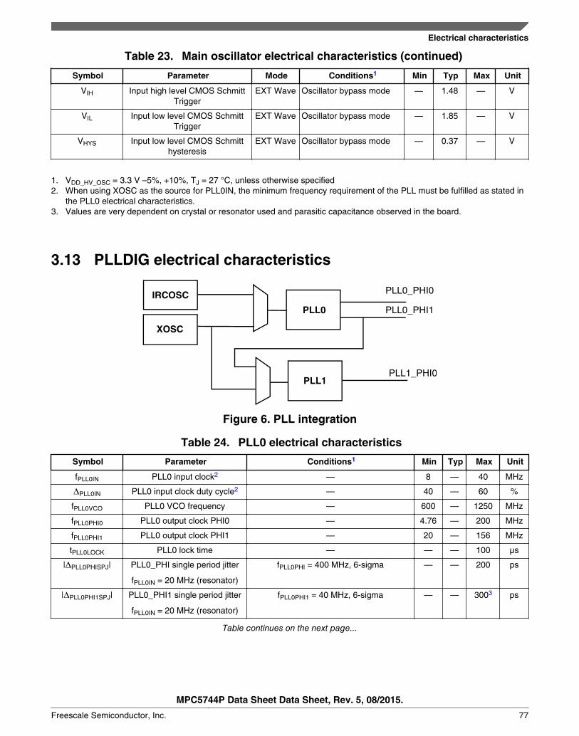
Table 23. Main oscillator electrical characteristics (continued)
Symbol Parameter Mode Conditions1 Min Typ Max Unit
VIH Input high level CMOS SchmittTrigger
EXT Wave Oscillator bypass mode — 1.48 — V
VIL Input low level CMOS SchmittTrigger
EXT Wave Oscillator bypass mode — 1.85 — V
VHYS Input low level CMOS Schmitthysteresis
EXT Wave Oscillator bypass mode — 0.37 — V
1. VDD_HV_OSC = 3.3 V –5%, +10%, TJ = 27 °C, unless otherwise specified2. When using XOSC as the source for PLL0IN, the minimum frequency requirement of the PLL must be fulfilled as stated in
the PLL0 electrical characteristics.3. Values are very dependent on crystal or resonator used and parasitic capacitance observed in the board.
3.13 PLLDIG electrical characteristics
|
IRCOSC
PLL0_PHI1 PLL0_PHI0
PLL1_PHI0
XOSC
PLL0
PLL1
Figure 6. PLL integration
Table 24. PLL0 electrical characteristics
Symbol Parameter Conditions1 Min Typ Max Unit
fPLL0IN PLL0 input clock2 — 8 — 40 MHz
PLL0IN PLL0 input clock duty cycle2 — 40 — 60 %
fPLL0VCO PLL0 VCO frequency — 600 — 1250 MHz
fPLL0PHI0 PLL0 output clock PHI0 — 4.76 — 200 MHz
fPLL0PHI1 PLL0 output clock PHI1 — 20 — 156 MHz
tPLL0LOCK PLL0 lock time — — — 100 µs
|PLL0PHISPJ| PLL0_PHI single period jitter
fPLL0IN = 20 MHz (resonator)
fPLL0PHI = 400 MHz, 6-sigma — — 200 ps
|PLL0PHI1SPJ| PLL0_PHI1 single period jitter
fPLL0IN = 20 MHz (resonator)
fPLL0PHI1 = 40 MHz, 6-sigma — — 3003 ps
Table continues on the next page...
Electrical characteristics
MPC5744P Data Sheet Data Sheet, Rev. 5, 08/2015.
Freescale Semiconductor, Inc. 77

Table 24. PLL0 electrical characteristics (continued)
Symbol Parameter Conditions1 Min Typ Max Unit
PLL0LTJ PLL0 output long term jitter3
fPLL0IN = 20 MHz (resonator),VCO frequency = 800 MHz
10 periods accumulated jitter (80 MHzequivalent frequency), 6-sigma pk-pk
— — ±250 ps
16 periods accumulated jitter (50 MHzequivalent frequency), 6-sigma pk-pk
— — ±300 ps
long term jitter (< 1 MHz equivalentfrequency), 6-sigma pk-pk)
— — ±500 ps
IPLL0 PLL0 consumption FINE LOCK state — — 5 mA
1. VDD_LV =1.25 V ± 5%, TJ = -40 to 165 °C unless otherwise specified.2. PLL0IN clock retrieved directly from either IRCOSC or external XOSC clock. Input characteristics are granted when using
IRCOSC or when external oscillator is used in functional mode.3. VDD_LV noise due to application in the range VDD_LV = 1.25 V±5%, with frequency below PLL bandwidth (40 kHz) will be
filtered.
Table 25. FMPLL1 electrical characteristics
Symbol Parameter Conditions1 Min Typ Max Unit
fPLL1IN PLL1 input clock2 — 38 — 78 MHz
PLL1IN PLL0 input clock duty cycle2 — 35 — 65 %
fPLL1VCO PLL1 VCO frequency — 600 — 1250 MHz
fPLL1PHI0 PLL1 output clock PHI0 — 4.76 — 200 MHz
tPLL1LOCK PLL1 lock time — — — 100 µs
fPLL1MOD PLL1 modulation frequency — — — 250 kHz
|δPLL1MOD| PLL1 modulation depth (when enabled) Center spread 0.25 — 2 %
Down spread 0.5 — 4 %
IPLL1 PLL1 consumption FINE LOCK state — — 6 mA
1. VDD_LV = 1.25 V ± 5%, TJ = -40 to 165 °C unless otherwise specified.2. PLL1IN clock retrieved directly from either internal PLL0 or external XOSC clock. Input characteristics are granted when
using internal PLL0 or when external oscillator is used in functional mode.
3.14 16 MHz Internal RC Oscillator (IRCOSC) electricalspecifications
NOTEUnless stated otherwise, specifications in Table 26 assume thefollowing: VDD_HV_PMU=3.15V to 3.6V, VSS=0V,VDD_LV=1.18V to 1.32V, VSS=0V, TJ=–40 to 165°C.
Table 26. Internal RC Oscillator electrical specifications
Symbol Parameter Conditions Min Typ Max Unit
FTarget IRCOSC target frequency — — 16 — MHz
Table continues on the next page...
Electrical characteristics
MPC5744P Data Sheet Data Sheet, Rev. 5, 08/2015.
78 Freescale Semiconductor, Inc.

Table 26. Internal RC Oscillator electrical specifications (continued)
Symbol Parameter Conditions Min Typ Max Unit
FUntrimmed IRCOSC frequency (untrimmed) — 9.6 — 24 MHz
δFvar_noT1 IRC frequency variation without temperature
compensationTJ < 150 °C –8 — 8 %
TJ < 165 °C –10 — 10
Tstartup Startup time without temperature compensation — — — 5 µs
IVDD3 Current consumption on 3.3 V power supply After Tstartup — — 55 µA
IVDD12 Current consumption on 1.2 V power supply After Tstartup — — 270 µA
1. The typical user trim step size (dfTRIM) is +48kHz for frequencies trimmed above nominal and -40kHz for frequenciestrimmed below nominal based on characterization results.
3.15 ADC electrical characteristics
The device provides a 12-bit Successive Approximation Register (SAR) Analog-to-Digital Converter.
( 2 )
( 1)
(3 ) (4)
(5)
Offset Error OSE
Offset Error OSE
Gain Error GE
1 LSB (ideal)
Vin(A) (LSBideal)
(1) Example of an actual transfer curve (2) The ideal transfer curve (3) Differential non-linearity error (DNL) (4) Integral non-linearity error (INL) (5) Center of a step of the actual transfer curve
code out
4095 4094 4093 4092 4091 4090
5 4 3 2 1
0
7 6
1 2 3 4 5 6 7 4089 4090 4091 4092 4093 4094 4095
1 LSB ideal =(VrefH-VrefL)/ 4096 = 3.3V/ 4096 = 0.806 mV Total Unadjusted Error TUE = +/- 6 LSB = +/- 4.84mV
Figure 7. ADC characteristics and error definitions
Electrical characteristics
MPC5744P Data Sheet Data Sheet, Rev. 5, 08/2015.
Freescale Semiconductor, Inc. 79

3.15.1 Input equivalent circuit and ADC conversion characteristics
RF
CF
RS RL RSW1
CP2
VDD_HV_ADREn
Sampling Source Filter Current Limiter
EXTERNAL CIRCUIT INTERNAL CIRCUIT SCHEME
RS Source Impedance RF Filter Resistance CF Filter Capacitance RL Current Limiter Resistance RSW1 Channel Selection Switch Impedance RAD Sampling Switch Impedance CP Pin Capacitance (two contributions, CP1 and CP2) CS Sampling Capacitance
CP1
RAD
Channel Selection
VA CS
Figure 8. Input equivalent circuit
NOTEUnless noted otherwise, the specifications in Table 27 assumethe use of 13-bit resolution: In ADC_CALBISTREG, setOPMODE to 110b.
Table 27. ADC conversion characteristics
Symbol Parameter Conditions1 Min Typ Max Unit
fCK ADC Clock frequency (depends on ADCconfiguration) (The duty cycle dependson AD_CK2 frequency.)
— 20 — 80 MHz
fs Sampling frequency — — — 1.00 MHz
tsample Sample time3 80 MHz, 12-bit resolution 250 — — ns
80 MHz, 13-bit resolution 250 — —
tconv Conversion time4 80 MHz, 12-bit resolution 650 — — ns
80 MHz, 13-bit resolution 700 — —
CS5 ADC input sampling capacitance — — 3 5 pF
CP15 ADC input pin capacitance 1 — — — 56 pF
CP25 ADC input pin capacitance 2 — — — 0.8 pF
RSW15 Internal resistance of analog source VREF range = 4.5 to 5.5 V — — 0.3 kΩ
VREF range = 3.15 to 3.6 V — — 875 Ω
Table continues on the next page...
Electrical characteristics
MPC5744P Data Sheet Data Sheet, Rev. 5, 08/2015.
80 Freescale Semiconductor, Inc.

Table 27. ADC conversion characteristics (continued)
Symbol Parameter Conditions1 Min Typ Max Unit
RAD5 Internal resistance of analog source — — — 825 Ω
INL Integral non-linearity — –2 — 2 LSB
DNL Differential non-linearity — –1 — 1 LSB
OFS Offset error — –4 — 4 LSB
GNE Gain error — –4 — 4 LSB
Input (single ADCchannel)
Max leakage 150 °C — — 250 nA
Max positive/negative injection — –3 — 3 mA
Input (doubleADC channel)
Max leakage 150 °C — — 300 nA
Max positive/negative injection |VREF_AD0 - VREF_AD1| <150mV
–3.6 — 3.6 mA
SNR7 Signal-to-noise ratio VREF = 3.3 V, Fin < 125kHz 67 — — dB
SNR7 Signal-to-noise ratio VREF = 5.0 V, Fin < 125kHz 69 — — dB
THD Total harmonic distortion Fin ≤ 125 kHz 65 70 — dB
ENOB Effective number of bits Fin < 125 kHz 10.5 — — bits
SINAD Signal-to-noise and distortion See ENOB (6.02 * ENOB) + 1.76 dB
TUEIS1WINJ Total unadjusted error for IS1WINJ(single ADC channels)
Without current injection –6 — 6 LSB
TUEIS1WINJ Total unadjusted error for IS1WINJ(single ADC channels)
Current injection: ±3 mA foreach channel, max 3channels
–8 — 8 LSB
1. VDD_HV_IO = 3.3 V -5%,+10%, TJ = –40 to +165 °C, unless otherwise specified, and analog input voltage from VAGND toVAREF
2. AD_CK clock is always half of the ADC module input clock defined via the auxiliary clock divider for the ADC.3. During the sample time the input capacitance CS can be charged/discharged by the external source. The internal
resistance of the analog source must allow the capacitance to reach its final voltage level within tsample. After the end of thesample time tsample, changes of the analog input voltage have no effect on the conversion result. Values for the sampleclock tsample depend on programming.
4. This parameter does not include the sample time tsample, but only the time for determining the digital result and the time toload the result register with the conversion result.
5. See Figure 8.6. For the 144-pin package.7. Test conditions have an influence on the achieved performance. Please contact FSL personnel to share the conditions for
these results.
NOTEThe ADC performance specifications are not guaranteed if twoADCs simultaneously sample the same shared channel.
Electrical characteristics
MPC5744P Data Sheet Data Sheet, Rev. 5, 08/2015.
Freescale Semiconductor, Inc. 81

Flash memory specifications
Maximum junction temperature 150°C
3.16.1.1 Flash memory program and erase specifications
NOTEAll timing, voltage, and current numbers specified in thissection are defined for a single embedded flash memory withinan SoC, and represent average currents for given supplies andoperations.
Table 28 shows the estimated Program/Erase times.
Table 28. Flash memory program and erase specifications
Symbol Characteristic1 Typ2 FactoryProgramming3, 4
Field Update Unit
InitialMax
InitialMax, Full
Temp
TypicalEnd ofLife5
Lifetime Max6
20°C ≤TA≤30°C
-40°C ≤TJ≤150°C
-40°C ≤TJ≤150°C
≤ 1,000cycles
≤ 250,000cycles
tdwpgm Doubleword (64 bits) program time 43 100 150 55 500 μs
tppgm Page (256 bits) program time 73 200 300 108 500 μs
tqppgn Quad-page (1024 bits) programtime
268 800 1,200 396 2,000 μs
t16kers 16 KB Block erase time 168 290 320 250 1,000 ms
t16kpgn 16 KB Block program time 34 45 50 40 1,000 ms
t32kers 32 KB Block erase time 217 360 390 310 1,200 ms
t32kpgm 32 KB Block program time 69 100 110 90 1,200 ms
t64kers 64 KB Block erase time 315 490 590 420 1,600 ms
t64kpgm 64 KB Block program time 138 180 210 170 1,600 ms
t256kers 256 KB Block erase time 884 1,520 2,030 1,080 4,000 — ms
t256kpgm 256 KB Block program time 552 720 880 650 4,000 — ms
1. Program times are actual hardware programming times and do not include software overhead. Block program timesassume quad-page programming.
2. Typical program and erase times represent the median performance and assume nominal supply values and operation at25 °C. Typical program and erase times may be used for throughput calculations.
3. Conditions: ≤ 150 cycles, nominal voltage.4. Plant Programing times provide guidance for timeout limits used in the factory.5. Typical End of Life program and erase times represent the median performance and assume nominal supply values.
Typical End of Life program and erase values may be used for throughput calculations.6. Conditions: -40°C ≤ TJ ≤ 150°C, full spec voltage.
3.16
3.16.1
Flash memory specifications
MPC5744P Data Sheet Data Sheet, Rev. 5, 08/2015.
82 Freescale Semiconductor, Inc.

3.16.1.2 Flash memory Array Integrity and Margin Read specificationsTable 29. Flash memory Array Integrity and Margin Read specifications
Symbol Characteristic Min Typical Max1 Units2
tai16kseq Array Integrity time for sequential sequence on 16KB block. — — 512 xTperiod x
Nread
—
tai32kseq Array Integrity time for sequential sequence on 32KB block. — — 1024 xTperiod x
Nread
—
tai64kseq Array Integrity time for sequential sequence on 64KB block. — — 2048 xTperiod x
Nread
—
tai256kseq Array Integrity time for sequential sequence on 256KB block. — — 8192 xTperiod x
Nread
—
tmr16kseq Margin Read time for sequential sequence on 16KB block. 73.81 — 110.7 μs
tmr32kseq Margin Read time for sequential sequence on 32KB block. 128.43 — 192.6 μs
tmr64kseq Margin Read time for sequential sequence on 64KB block. 237.65 — 356.5 μs
tmr256kseq Margin Read time for sequential sequence on 256KB block. 893.01 — 1,339.5 μs
1. Array Integrity times need to be calculated and is dependant on system frequency and number of clocks per read. Theequation presented require Tperiod (which is the unit accurate period, thus for 200 MHz, Tperiod would equal 5e-9) andNread (which is the number of clocks required for read, including pipeline contribution. Thus for a read setup that requires6 clocks to read with no pipeline, Nread would equal 6. For a read setup that requires 6 clocks to read, and has theaddress pipeline set to 2, Nread would equal 4 (or 6 - 2).)
2. The units for Array Integrity are determined by the period of the system clock. If unit accurate period is used in theequation, the results of the equation are also unit accurate.
3.16.1.3 Flash memory module life specificationsTable 30. Flash memory module life specifications
Symbol Characteristic Conditions Min Typical Units
Array P/Ecycles
Number of program/erase cycles per blockfor 16 KB, 32 KB and 64 KB blocks.1
— 250,000 — P/Ecycles
Number of program/erase cycles per blockfor 256 KB blocks.2
— 1,000 250,000 P/Ecycles
Dataretention
Minimum data retention. Blocks with 0 - 1,000 P/Ecycles.
50 — Years
Blocks with 100,000 P/Ecycles.
20 — Years
Blocks with 250,000 P/Ecycles.
10 — Years
1. Program and erase supported across standard temperature specs.2. Program and erase supported across standard temperature specs.
Maximum junction temperature 150°C
MPC5744P Data Sheet Data Sheet, Rev. 5, 08/2015.
Freescale Semiconductor, Inc. 83

3.16.1.4 Data retention vs program/erase cycles
Graphically, Data Retention versus Program/Erase Cycles can be represented by thefollowing figure. The spec window represents qualified limits. The extrapolated dottedline demonstrates technology capability, however is beyond the qualification limits.
3.16.1.5 Flash memory AC timing specificationsTable 31. Flash memory AC timing specifications
Symbol Characteristic Min Typical Max Units
tpsus Time from setting the MCR-PSUS bit until MCR-DONE bit is setto a 1.
— 7
plus foursystemclock
periods
9.1
plus foursystemclock
periods
μs
tesus Time from setting the MCR-ESUS bit until MCR-DONE bit is setto a 1.
— 16
plus foursystemclock
periods
20.8
plus foursystemclock
periods
μs
tres Time from clearing the MCR-ESUS or PSUS bit with EHV = 1until DONE goes low.
— — 100 ns
tdone Time from 0 to 1 transition on the MCR-EHV bit initiating aprogram/erase until the MCR-DONE bit is cleared.
— — 5 ns
Table continues on the next page...
Maximum junction temperature 150°C
MPC5744P Data Sheet Data Sheet, Rev. 5, 08/2015.
84 Freescale Semiconductor, Inc.

Table 31. Flash memory AC timing specifications (continued)
Symbol Characteristic Min Typical Max Units
tdones Time from 1 to 0 transition on the MCR-EHV bit aborting aprogram/erase until the MCR-DONE bit is set to a 1.
— 16
plus foursystemclock
periods
20.8
plus foursystemclock
periods
μs
tdrcv Time to recover once exiting low power mode. 16
plus sevensystemclock
periods.
— 45
plus sevensystemclock
periods
μs
taistart Time from 0 to 1 transition of UT0-AIE initiating a Margin Reador Array Integrity until the UT0-AID bit is cleared. This time alsoapplies to the resuming from a suspend or breakpoint byclearing AISUS or clearing NAIBP
— — 5 ns
taistop Time from 1 to 0 transition of UT0-AIE initiating an ArrayIntegrity abort until the UT0-AID bit is set. This time also appliesto the UT0-AISUS to UT0-AID setting in the event of a ArrayIntegrity suspend request.
— — 80
plus fifteensystemclock
periods
ns
tmrstop Time from 1 to 0 transition of UT0-AIE initiating a Margin Readabort until the UT0-AID bit is set. This time also applies to theUT0-AISUS to UT0-AID setting in the event of a Margin Readsuspend request.
10.36
plus foursystemclock
periods
— 20.42
plus foursystemclock
periods
μs
Maximum junction temperature 165°C
3.16.2.1 Flash memory program and erase specifications
NOTEAll timing, voltage, and current numbers specified in thissection are defined for a single embedded flash memory withinan SoC, and represent average currents for given supplies andoperations.
Table 32 shows the estimated Program/Erase times.
3.16.2
Maximum junction temperature 165°C
MPC5744P Data Sheet Data Sheet, Rev. 5, 08/2015.
Freescale Semiconductor, Inc. 85

Table 32. Flash memory program and erase specifications
Symbol Characteristic1 Typ2 Factory Programming3, 4 Field Update Units
Initial Max Initial Max
Full Temp
Typical End ofLife5
Lifetime Max6
20°C≤ TA ≤30°C4
–40°C≤ TJ ≤150°C4
–40°C≤ TJ ≤165 °C
≤1,000
cycles
≤250,000cycles
tdwpgm Doubleword (64 bits)program time
43 100 150 65 650 μs
tppgm Page (256 bits)program time
73 200 300 145 650 μs
tqppgn Quad-page (1024 bits)program time
268 800 1,200 540 2,700 μs
t16kers 16 KB Block erase time 168 290 320 500 9,000 ms
t16kpgn 16 KB Block programtime
34 45 50 70 1,400 ms
t32kers 32 KB Block erase time 217 360 390 610 9,000 ms
t32kpgm 32 KB Block programtime
69 100 110 140 2,800 ms
t64kers 64 KB Block erase time 315 490 590 820 9,000 ms
t64kpgm 64 KB Block programtime
138 180 210 280 5,500 ms
t256kers 256 KB Code erasetime7
884 1,520 2,030 1,080 4,000 — ms
t256kpgm 256 KB Code programtime7
552 720 880 650 4,000 — ms
1. Program times are actual hardware programming times and do not include software overhead. Block program timesassume quad-page programming.
2. Typical program and erase times represent the median performance and assume nominal supply values and operation at25 °C. Typical program and erase times may be used for throughput calculations.
3. Conditions: ≤ 150 cycles, nominal voltage.4. Plant Programing times provide guidance for timeout limits used in the factory.5. Typical End of Life program and erase times represent the median performance and assume nominal supply values.
Typical End of Life program and erase values may be used for throughput calculations.6. Conditions: –40°C ≤ TJ ≤ 165°C; full spec voltage. 16 KB, 32 KB and 64 KB blocks are allowed to be programmed or
erased up to TJ = 165°C with restrictions.7. 256 KB blocks may be programmed or erased at TJ = 150°C maximum. Times listed on this row are TJ = 150°C times.
3.16.2.2 Flash memory Array Integrity and Margin Read specificationsTable 33. Flash memory Array Integrity and Margin Read specifications
Symbol Characteristic Min Typical Max1 Units2
tai16kseq Array Integrity time for sequential sequence on 16KB block. — — 512 xTperiod x
Nread
—
Table continues on the next page...
Maximum junction temperature 165°C
MPC5744P Data Sheet Data Sheet, Rev. 5, 08/2015.
86 Freescale Semiconductor, Inc.

Table 33. Flash memory Array Integrity and Margin Read specifications (continued)
Symbol Characteristic Min Typical Max1 Units2
tai32kseq Array Integrity time for sequential sequence on 32KB block. — — 1024 xTperiod x
Nread
—
tai64kseq Array Integrity time for sequential sequence on 64KB block. — — 2048 xTperiod x
Nread
—
tai256kseq Array Integrity time for sequential sequence on 256KB block. — — 8192 xTperiod x
Nread
—
tmr16kseq Margin Read time for sequential sequence on 16KB block. 73.81 — 110.7 μs
tmr32kseq Margin Read time for sequential sequence on 32KB block. 128.43 — 192.6 μs
tmr64kseq Margin Read time for sequential sequence on 64KB block. 237.65 — 356.5 μs
tmr256kseq Margin Read time for sequential sequence on 256KB block. 893.01 — 1,339.5 μs
1. Array Integrity times need to be calculated and is dependant on system frequency and number of clocks per read. Theequation presented require Tperiod (which is the unit accurate period, thus for 200 MHz, Tperiod would equal 5e-9) andNread (which is the number of clocks required for read, including pipeline contribution. Thus for a read setup that requires6 clocks to read with no pipeline, Nread would equal 6. For a read setup that requires 6 clocks to read, and has theaddress pipeline set to 2, Nread would equal 4 (or 6 - 2).)
2. The units for Array Integrity are determined by the period of the system clock. If unit accurate period is used in theequation, the results of the equation are also unit accurate.
3.16.2.3 Flash memory module life specificationsTable 34. Flash memory module life specifications
Symbol Characteristic Conditions Min Typical Units
Array P/Ecycles
Number of program/erase cycles per blockfor 16 KB, 32 KB and 64 KB blocks.1
- 250,000 - P/Ecycles
Number of program/erase cycles per blockfor 256 KB blocks.2
- 1,000 250,000 P/Ecycles
Dataretention
Minimum data retention. Blocks with 0 - 1,000 P/Ecycles.
50 - Years
Blocks with 100,000 P/Ecycles.
20 - Years
Blocks with 250,000 P/Ecycles.
10 - Years
1. Program and erase supported across standard temperature specs. Up to 10,000 program and erase cycles may be donebetween 150 °C and 165 °C out of the total specified number of cycles.
2. Program and erase supported across standard temperature specs.
3.16.2.4 Data retention vs program/erase cycles
Graphically, Data Retention versus Program/Erase Cycles can be represented by thefollowing figure. The spec window represents qualified limits. The extrapolated dottedline demonstrates technology capability, however is beyond the qualification limits.
Maximum junction temperature 165°C
MPC5744P Data Sheet Data Sheet, Rev. 5, 08/2015.
Freescale Semiconductor, Inc. 87

3.16.2.5 Flash memory AC timing specificationsTable 35. Flash memory AC timing specifications
Symbol Characteristic Min Typical Max Units
tpsus Time from setting the MCR-PSUS bit until MCR-DONE bit is setto a 1.
— 7 plus foursystemclock
periods
9.1 plusfour
systemclock
periods
μs
tesus Time from setting the MCR-ESUS bit until MCR-DONE bit is setto a 1.
— 16 plusfour
systemclock
periods
20.8 plusfour
systemclock
periods
μs
tres Time from clearing the MCR-ESUS or PSUS bit with EHV = 1until DONE goes low.
— — 100 ns
tdone Time from 0 to 1 transition on the MCR-EHV bit initiating aprogram/erase until the MCR-DONE bit is cleared.
— — 5 ns
tdones Time from 1 to 0 transition on the MCR-EHV bit aborting aprogram/erase until the MCR-DONE bit is set to a 1.
— 16 plusfour
systemclock
periods
20.8 plusfour
systemclock
periods
μs
Table continues on the next page...
Maximum junction temperature 165°C
MPC5744P Data Sheet Data Sheet, Rev. 5, 08/2015.
88 Freescale Semiconductor, Inc.

Table 35. Flash memory AC timing specifications (continued)
Symbol Characteristic Min Typical Max Units
tdrcv Time to recover once exiting low power mode. 16 plussevensystemclock
periods.
— 45 plussevensystemclock
periods
μs
taistart Time from 0 to 1 transition of UT0-AIE initiating a Margin Reador Array Integrity until the UT0-AID bit is cleared. This time alsoapplies to the resuming from a suspend or breakpoint byclearing AISUS or clearing NAIBP
— — 5 ns
taistop Time from 1 to 0 transition of UTO-AIE initiating an ArrayIntegrity abort until the UT0-AID bit is set. This time also appliesto the UT0-AISUS to UT0-AID setting in the event of a ArrayIntegrity suspend request.
— — 80
plus fifteensystemclock
periods
ns
tmrstop Time from 1 to 0 transition of UTO-AIE initiating a Margin Readabort until the UT0-AID bit is set. This time also applies to theUT0-AISUS to UT0-AID setting in the event of a Margin Readsuspend request.
10.36
plus foursystemclock
periods
— 20.42
plus foursystemclock
periods
μs
3.16.3 Flash memory read wait-state and address-pipeline controlsettings
The following table describes the recommended settings of the Flash MemoryController's PFCR1[RWSC] and PFCR1[APC] fields at various operating frequencies,based on specified intrinsic flash memory access times of the C55FMC array at 150°C.
NOTEIf the user does not follow these recommended settings, the usermust run the flash memory's array integrity (AI) check withbreakpoints disabled: Set the Array Integrity Break PointEnable bit in the C55FMC's UTest 0 register(C55FMC_UT0[AIBPE]) to 0.
Table 36. Flash memory read wait-state and address-pipeline controlcombinations
Operating frequency (fCPU = SYS_CLK)
RWSC APC
Flash read latencyon mini-cache miss
(# of fCPU clockperiods)
Flash read latencyon mini-cache hit(# of fCPU clock
periods)–40°C to 150°C Max 165°C option
0 MHz < fCPU ≤ 33 MHz 0 MHz < fCPU ≤ 30 MHz 0 0 3 1
33 MHz < fCPU ≤ 100 MHz 30 MHz < fCPU ≤ 90 MHz 2 1 5 1
Table continues on the next page...
Maximum junction temperature 165°C
MPC5744P Data Sheet Data Sheet, Rev. 5, 08/2015.
Freescale Semiconductor, Inc. 89

Table 36. Flash memory read wait-state and address-pipeline control combinations(continued)
Operating frequency (fCPU = SYS_CLK)
RWSC APC
Flash read latencyon mini-cache miss
(# of fCPU clockperiods)
Flash read latencyon mini-cache hit(# of fCPU clock
periods)–40°C to 150°C Max 165°C option
100 MHz < fCPU ≤ 133 MHz 90 MHz < fCPU ≤ 120 MHz 3 1 6 1
133 MHz < fCPU ≤ 167 MHz 120 MHz < fCPU ≤ 150 MHz 4 1 7 1
167 MHz < fCPU ≤ 200 MHz 150 MHz < fCPU ≤ 180 MHz 5 2 8 1
3.17 SGEN electrical characteristicsTable 37. SGEN electrical characteristics
Symbol Parameter Min Max Unit
Input clock 12 20 MHz
SINAD Signal-to-noise ratio plus distortion 50 — dB
FREQ Frequency range of the sine wave 1 50 kHz
FRP Frequency precision of the sine wave (peak to peak variation) –5 5 %
APP Sine wave amplitude (peak to peak) 0.426 2.063 V
Load Load capacitance 25 100 pF
Current Output current — 100 µA
TJ Junction temperature –40 165 °C
3.18 RESET sequence duration
This following table shows the duration of different reset sequences. See the chip'sReference Manual for details about the reset sequences.
Table 38. RESET sequences
Symbol Parameter Conditions TReset Unit
Min Typ Max1
TDRB 'Destructive' reset sequence, BIST enabled Self test clock in STCU isthe PLL generated clock.Self test configuration as
per DCF recordprogramming. For four
LBIST partitions in design,two LBIST partitions are
run in parallel.
— — 18.0 ms
TDR 'Destructive' reset sequence, BIST disabled — — 440 480 μs
Table continues on the next page...
Maximum junction temperature 165°C
MPC5744P Data Sheet Data Sheet, Rev. 5, 08/2015.
90 Freescale Semiconductor, Inc.

Table 38. RESET sequences (continued)
Symbol Parameter Conditions TReset Unit
Min Typ Max1
TERLB External reset sequence—long, BIST enabled Self test clock in STCU isthe PLL generated clock.Self test configuration as
per DCF recordprogramming. For four
LBIST partitions in design,two LBIST partitions are
run in parallel.
— — 17.5 ms
TERL External reset sequence—long, BIST disabled — — 120 150 μs
TFRL Functional reset sequence—long — — 165 180 μs
TFRS Functional reset sequence—short — — 10.0 12.0 μs
1. The maximum value applies only if the reset sequence duration is not prolonged by an extended assertion of RESET_B byan external reset generator.
3.19 AC specificationsAC Parameters are specified over the full operating junction temperature range of -40°Cto +165°C and for the full operating range of the VDD_IO supply defined in DC electricalcharacteristics.
Table 39. Functional Pad AC Specifications
Symbol Prop. Delay (ns)1
L>H/H>L
Rise/Fall Edge (ns) Drive Load(pF)
SIUL2_MSCRn'sSRC[1:0] field
Min Max Min Max MSB,LSB
I/O (output) 2.5/2.5 7.5/7.5 0.9/0.9 3/3 50 11
— — — 12/12 200
— 8/8 — 3.5/3.5 25 10
— 11.5/11.5 — 6.5/6.5 50
— — — 30/30 200
— 45/45 — 25/25 50 012
— 65/65 — 30/30 200
— 75/75 — 40/40 50 002
— 110/110 — 50/50 200
I/O (input) — 1.5/1.5 — 0.5/0.5 0.5 NA
1. As measured from 50% of core side input to Voh/Vol of the output2. Slew rate control modes
Maximum junction temperature 165°C
MPC5744P Data Sheet Data Sheet, Rev. 5, 08/2015.
Freescale Semiconductor, Inc. 91

3.19.1 Reset pad (EXT_POR, RESET) electrical characteristics
The device implements a dedicated bidirectional RESET pin.
VIL
VDD_HV_IOx
device reset forced by PORST
VDDMIN
PORST
VIH
device start-up phase
AAA
IO
Figure 9. Start-up reset requirements
VPORST
VIL
VIH
VDD_HV_IO
filtered by hysteresis
filtered by lowpass filter
WFRST
WNFRST
hw_rst
‘1’
‘0’filtered by lowpass filter
WFRST
unknown resetstate device under hardware reset
IO
Figure 10. Noise filtering on reset signal
Maximum junction temperature 165°C
MPC5744P Data Sheet Data Sheet, Rev. 5, 08/2015.
92 Freescale Semiconductor, Inc.

Table 40. Reset (RESET) electrical characteristics
Symbol Parameter Conditions1 Value Unit
Min Typ Max
VIH Input high level TTL (Schmitt Trigger) — 2.0 — VDD_HV_IO
+ 0.4
V
VIL Input low level TTL (Schmitt Trigger) — –0.4 — 0.8 V
VHYS Input hysteresis TTL (Schmitt Trigger) — 300 — — mV
IOL_R Strong pull-down current Device under power-on reset
VDD_HV_A=1.0 V
VOL = 0.35*VDD_HV_IO
0.2 — — mA
Device under power-on reset
VDD_HV_IO=3.0 V
VOL = 0.35*VDD_HV_IO
15 — — mA
WFRST (RESET)-input filtered pulse — — — 500 ns
WNFRST (RESET)-input not filtered pulse — 2 — — µs
|IWPD| Weak pull-down current absolute value RESET pin
VIN = VDD
30 — 80 µA
1. VDD_HV_IO = 3.3 V -5%,+10%, TJ = –40 to 165 °C, unless otherwise specified
Table 41. Reset (EXT_POR) electrical characteristics
Symbol Parameter Conditions Value Unit
Min Typ Max
WFPORST PORST input filtered pulse — — — 500 ns
WNFPORST PORST input not filtered pulse — 2000 — — ns
WIH Input high level — 2 — VDD_HV_IO
+0.4
V
WIL Input low level — -0.4 — 0.8 V
3.19.2 WKUP/NMI timingTable 42. WKUP/NMI glitch filter
Symbol Parameter Min Typ Max Unit
WFNMI NMI pulse width that is rejected — — 20 ns
WNFNMI NMI pulse width that is passed 400 — — ns
3.19.3 Debug/JTAG/Nexus/Aurora timing
Maximum junction temperature 165°C
MPC5744P Data Sheet Data Sheet, Rev. 5, 08/2015.
Freescale Semiconductor, Inc. 93

3.19.3.1 JTAG interface timingTable 43. JTAG pin AC electrical characteristics 1
# Symbol Characteristic Min Max Unit
1 tJCYC TCK Cycle Time2 36 — ns
2 tJDC TCK Clock Pulse Width 40 60 %
3 tTCKRISE TCK Rise and Fall Times (40% - 70%) — 3 ns
4 tTMSS, tTDIS TMS, TDI Data Setup Time 5 — ns
5 tTMSH, tTDIH TMS, TDI Data Hold Time 5 — ns
6 tTDOV TCK Low to TDO Data Valid — 153 ns
7 tTDOI TCK Low to TDO Data Invalid 0 — ns
8 tTDOHZ TCK Low to TDO High Impedance — 15 ns
9 tJCMPPW JCOMP Assertion Time 100 — ns
10 tJCMPS JCOMP Setup Time to TCK Low 40 — ns
11 tBSDV TCK Falling Edge to Output Valid — 6004 ns
12 tBSDVZ TCK Falling Edge to Output Valid out of HighImpedance
— 600 ns
13 tBSDHZ TCK Falling Edge to Output High Impedance — 600 ns
14 tBSDST Boundary Scan Input Valid to TCK Rising Edge 15 — ns
15 tBSDHT TCK Rising Edge to Boundary Scan Input Invalid 15 — ns
1. These specifications apply to JTAG boundary scan only.2. This timing applies to TDI, TDO, TMS pins, however, actual frequency is limited by pad type for EXTEST instructions.
Refer to pad specification for allowed transition frequency3. Timing includes TCK pad delay, clock tree delay, logic delay and TDO output pad delay.4. Applies to all pins, limited by pad slew rate. Refer to IO delay and transition specification and add 20 ns for JTAG delay.
TCK
1
2
2
3
3
Figure 11. JTAG test clock input timing
Maximum junction temperature 165°C
MPC5744P Data Sheet Data Sheet, Rev. 5, 08/2015.
94 Freescale Semiconductor, Inc.

TCK
4
5
6
7 8
TMS, TDI
TDO
Figure 12. JTAG test access port timing
TCK
JCOMP
9
10
Figure 13. JTAG JCOMP timing
Maximum junction temperature 165°C
MPC5744P Data Sheet Data Sheet, Rev. 5, 08/2015.
Freescale Semiconductor, Inc. 95

TCK
OutputSignals
InputSignals
OutputSignals
11
12
13
14
15
Figure 14. JTAG boundary scan timing
3.19.3.2 Nexus timingTable 44. Nexus debug port timing 1
No. Symbol Parameter Conditions Min Max Unit
1 tMCYC MCKO Cycle Time — 15.6 — ns
2 tMDC MCKO Duty Cycle — 40 60 %
3 tMDOV MCKO Low to MDO, MSEO, EVTO DataValid2
— –0.1 0.25 tMCYC
4 tEVTIPW EVTI Pulse Width — 4 — tTCYC
5 tEVTOPW EVTO Pulse Width — 1 — tMCYC
6 tTCYC TCK Cycle Time3 — 62.5 — ns
7 tTDC TCK Duty Cycle — 40 60 %
8 tNTDIS, tNTMSS TDI, TMS Data Setup Time — 8 — ns
9 tNTDIH, tNTMSH TDI, TMS Data Hold Time — 5 — ns
10 tJOV TCK Low to TDO/RDY Data Valid — 0 25 ns
Maximum junction temperature 165°C
MPC5744P Data Sheet Data Sheet, Rev. 5, 08/2015.
96 Freescale Semiconductor, Inc.

1. JTAG specifications in this table apply when used for debug functionality. All Nexus timing relative to MCKO is measuredfrom 50% of MCKO and 50% of the respective signal.
2. For all Nexus modes except DDR mode, MDO, MSEO, and EVTO data is held valid until next MCKO low cycle.3. The system clock frequency needs to be four times faster than the TCK frequency.
1
2
MCKO
MDOMSEOEVTO
Output Data Valid
3
5
Figure 15. Nexus output timing
EVTI4
Figure 16. Nexus EVTI Input Pulse Width
Maximum junction temperature 165°C
MPC5744P Data Sheet Data Sheet, Rev. 5, 08/2015.
Freescale Semiconductor, Inc. 97

TDO/RDY
8
9
TMS, TDI
10
TCK
6
7
Figure 17. Nexus TDI, TMS, TDO timing
3.19.3.3 Aurora LVDS driver electrical characteristicsTable 45. Aurora LVDS driver electrical characteristics
Symbol Parameter1 Value Unit
Min Typ Max
Data Rate
DATARATE Data rate — 1250 Typ+0.1% Mbps
STARTUP
TSTRT_BIAS Bias startup time2 — — 5 µs
TSTRT_TX Transmitter startup time3 — — 5 µs
TSTRT_RX Receiver startup time4 — — 4 µs
1. Conditions for these values are VDD_HV_IO = 3.3 V (–5%, +10%), TJ = –40 to 150 °C2. Startup time is defined as the time taken by LVDS current reference block for settling bias current after its pwr_down
(power down) has been deasserted. LVDS functionality is guaranteed only after the startup time.
Maximum junction temperature 165°C
MPC5744P Data Sheet Data Sheet, Rev. 5, 08/2015.
98 Freescale Semiconductor, Inc.
3. Startup time is defined as the time taken by LVDS transmitter for settling after its pwr_down (power down) has beendeasserted. Here it is assumed that current reference is already stable (see Bias start-up time). LVDS functionality isguaranteed only after the startup time.
4. Startup time is defined as the time taken by LVDS receiver for settling after its pwr_down (power down) has beendeasserted. Here it is assumed that current reference is already stable (see Bias start-up time). LVDS functionality isguaranteed only after the startup time.
3.19.3.4 Nexus Aurora debug port timingTable 46. Nexus Aurora debug port timing
# Symbol Characteristic Min Max Unit
1 tREFCLK Reference clock frequency 625 1250 MHz
2 tRCDC Reference Clock Duty Cycle 45 55 %
3 JRC Reference Clock jitter — 40 ps
4 tSTABILITY Reference Clock Stability 50 — PPM
5 BER Bit Error Rate — 10-12 —
6 JD Transmit lane Deterministic Jitter — 0.17 OUI
7 JT Transmit lane Total Jitter — 0.35 OUI
8 SO Differential output skew — 20 ps
9 SMO Lane to lane output skew — 1000 ps
10 UI Aurora lane Unit Interval 800 1600 ps
Maximum junction temperature 165°C
MPC5744P Data Sheet Data Sheet, Rev. 5, 08/2015.
Freescale Semiconductor, Inc. 99

Tx Data [m]
Zero Crossover
CLOCKREF -
CLOCKREF +
2
Zero Crossover
2
1
Tx Data -
Tx Data +
Ideal Zero Crossover
Tx Data [n]
Zero Crossover
Tx Data [n+1]
Zero Crossover
99
88 8
Figure 18. Nexus Aurora timings
Rise/fall timing for the Nexus Aurora debug port reference clock must conform to thearea between the minimum and maximum value ranges shown in the following receiver"eye" diagram.
Maximum junction temperature 165°C
MPC5744P Data Sheet Data Sheet, Rev. 5, 08/2015.
100 Freescale Semiconductor, Inc.

Figure 19. Nexus Aurora receiver "eye" diagram
3.19.4 External interrupt timing (IRQ pin)Table 47. External interrupt timing
# Symbol Parameter Conditions Min Max Unit
1 tIPWL IRQ pulse width low — 3 — tCYC
2 tIPWH IRQ pulse width high — 3 — tCYC
3 tICYC IRQ edge to edge time1 — 6 — tCYC
1. Applies when IRQ pins are configured for rising edge or falling edge events, but not both
Maximum junction temperature 165°C
MPC5744P Data Sheet Data Sheet, Rev. 5, 08/2015.
Freescale Semiconductor, Inc. 101

IRQ
1
2
3
Figure 20. External interrupt timing
3.19.5 SPI timingTable 48. SPI timing
# Symbol Parameter Conditions Min Max Unit
1 tSCK SPI cycle time Master (MTFE = 0) 40 — ns
Slave (MTFE = 0) 40 —
Slave Receive Only Mode1 16 —
2 tCSC PCS to SCK delay — 16 — ns
3 tASC After SCK delay — 16 — ns
4 tSDC SCK duty cycle — tSCK/2 – 4 tSCK/2 + 4 ns
5 tA Slave access time SS active to SOUT valid — 40 ns
6 tDIS Slave SOUT disabletime
SS inactive to SOUT High-Z or invalid — 25 ns
7 tPCSC PCSx to PCSS time — 13 — ns
8 tPASC PCSS to PCSx time — 13 — ns
9 tSUI Data setup time forinputs
Master (MTFE = 0) 16 — ns
Slave 2 —
Master (MTFE = 1, CPHA = 0) 16 – (P2 xtSYS
, 3)—
Master (MTFE = 1, CPHA = 1) 16 —
10 tHI Data hold time forinputs
Master (MTFE = 0) –3 — ns
Slave 4 —
Master (MTFE = 1, CPHA = 0) –3 + (P2 xtSYS
, 3)—
Master (MTFE = 1, CPHA = 1) –3 —
11 tSUO Data valid (after SCKedge) time for outputs
Master (MTFE = 0) — 4 ns
Slave — 17
Master (MTFE = 1, CPHA = 0) — 4 + tSYS3
Master (MTFE = 1, CPHA = 1) — 4
Table continues on the next page...
Maximum junction temperature 165°C
MPC5744P Data Sheet Data Sheet, Rev. 5, 08/2015.
102 Freescale Semiconductor, Inc.
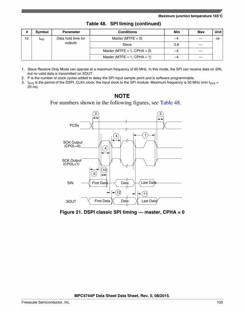
Table 48. SPI timing (continued)
# Symbol Parameter Conditions Min Max Unit
12 tHO Data hold time foroutputs
Master (MTFE = 0) –4 — ns
Slave 3.6 —
Master (MTFE = 1, CPHA = 0) –4 —
Master (MTFE = 1, CPHA = 1) –4 —
1. Slave Receive Only Mode can operate at a maximum frequency of 60 MHz. In this mode, the SPI can receive data on SIN,but no valid data is transmitted on SOUT.
2. P is the number of clock cycles added to delay the SPI input sample point and is software programmable.3. tSYS is the period of the DSPI_CLKn clock, the input clock to the SPI module. Maximum frequency is 50 MHz (min tSYS =
20 ns).
NOTEFor numbers shown in the following figures, see Table 48.
Data Last DataFirst Data
First Data Data Last Data
SIN
SOUT
PCSx
SCK Output
4
9
12
1
11
10
4
SCK Output
(CPOL=0)
(CPOL=1)
32
Figure 21. DSPI classic SPI timing — master, CPHA = 0
Maximum junction temperature 165°C
MPC5744P Data Sheet Data Sheet, Rev. 5, 08/2015.
Freescale Semiconductor, Inc. 103

Data Last DataFirst DataSIN
SOUT
12 11
10
Last DataDataFirst Data
SCK Output
SCK Output
PCSx
9
(CPOL=0)
(CPOL=1)
Figure 22. DSPI classic SPI timing — master, CPHA = 1
Last DataFirst Data
3
4
1
Data
Data
SIN
SOUT
SS
4
5 6
9
11
10
12
SCK Input
First Data Last Data
SCK Input
2
(CPOL=0)
(CPOL=1)
Figure 23. DSPI classic SPI timing — slave, CPHA = 0
Maximum junction temperature 165°C
MPC5744P Data Sheet Data Sheet, Rev. 5, 08/2015.
104 Freescale Semiconductor, Inc.

5 6
9
12
11
10
Last Data
Last DataSIN
SOUT
SS
First Data
First Data
Data
Data
SCK Input
SCK Input
(CPOL=0)
(CPOL=1)
Figure 24. DSPI classic SPI timing — slave, CPHA = 1
PCSx
3
14
10
4
9
12 11
SCK Output
SCK Output
SIN
SOUT
First Data Data Last Data
First Data Data Last Data
2
(CPOL=0)
(CPOL=1)
Figure 25. DSPI modified transfer format timing — master, CPHA = 0
Maximum junction temperature 165°C
MPC5744P Data Sheet Data Sheet, Rev. 5, 08/2015.
Freescale Semiconductor, Inc. 105
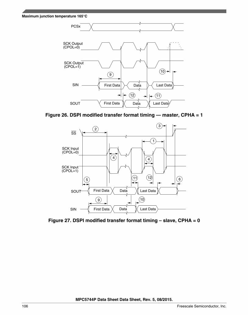
PCSx
109
12 11
SCK Output
SCK Output
SIN
SOUT
First Data Data Last Data
First Data Data Last Data
(CPOL=0)
(CPOL=1)
Figure 26. DSPI modified transfer format timing — master, CPHA = 1
Last DataFirst Data
3
4
1
Data
Data
SIN
SOUT
SS
4
5 6
9
11
10
SCK Input
First Data Last Data
SCK Input
2
(CPOL=0)
(CPOL=1)
12
Figure 27. DSPI modified transfer format timing – slave, CPHA = 0
Maximum junction temperature 165°C
MPC5744P Data Sheet Data Sheet, Rev. 5, 08/2015.
106 Freescale Semiconductor, Inc.

5 6
9
12
11
10
Last Data
Last DataSIN
SOUT
SS
First Data
First Data
Data
Data
SCK Input
SCK Input
(CPOL=0)
(CPOL=1)
Figure 28. DSPI modified transfer format timing — slave, CPHA = 1
PCSx
7 8
PCSS
Figure 29. DSPI PCS strobe (PCSS) timing
3.19.6 LFAST
Maximum junction temperature 165°C
MPC5744P Data Sheet Data Sheet, Rev. 5, 08/2015.
Freescale Semiconductor, Inc. 107

3.19.6.1 LFAST interface timing diagrams
Figure 30. LFAST timing definition
Maximum junction temperature 165°C
MPC5744P Data Sheet Data Sheet, Rev. 5, 08/2015.
108 Freescale Semiconductor, Inc.

Data Validpad_p/pad_nDifferential TXData Lines
H
L
Tsu
lfast_pwr_down
Figure 31. Power-down exit time
Differential TXData Lines
pad_p/pad_n
TriseTfall
90%
10%
VIH
VIL
Figure 32. Rise/fall time
3.19.6.2 LFAST interface electrical characteristicsTable 49. LFAST electrical characteristics
Symbol Parameter Conditions1 Value Unit
Min Typ Max
VDD_HV_IO Operating supply conditions 3.15 — 3.6 V
Data Rate
DATARATE Data rate — — 312/320 Typ+0.1% Mbps
STARTUP
TSTRT_BIAS Bias startup time2 — — 0.5 3 µs
TPD2NM_TX Transmitter startup time (powerdown to normal mode)3
— — 0.2 2 µs
TSM2NM_TX Transmitter startup time (sleepmode to normal mode)4
— — 0.2 0.5 µs
TPD2NM_RX Receiver startup time5 (Power downto Normal mode)
— — 20 40 ns
TPD2SM_RX Receiver startup time4 (Power downto Sleep mode)
— — 20 50 ns
Table continues on the next page...
Maximum junction temperature 165°C
MPC5744P Data Sheet Data Sheet, Rev. 5, 08/2015.
Freescale Semiconductor, Inc. 109

Table 49. LFAST electrical characteristics(continued)
Symbol Parameter Conditions1 Value Unit
Min Typ Max
TRANSMITTER
VOS_DRF Common mode voltage — 1.18 — 1.32 V
|ΔVOD_DRF| Differential output voltage swing(terminated)
— ±100 ±200 ± 285 mV
TTR_DRF Rise/Fall time (10% - 90% of swing) — 0.26 — 1.5 ns
ROUT_DRF Terminating resistance — 67 — 198 Ω
COUT_DRF Capacitance6 — — — 5 pF
RECEIVER
VICOM_DRF Common mode voltage — 0.157 — 1.68 V
|DVI_DRF| Differential input voltage — 100 — — mV
VHYS_DRF Input hysteresis — 25 — — mV
RIN_DRF Terminating resistance — 80 115 150 Ω
CIN_DRF Capacitance9 — — 3.5 6 pF
LIN_DRF Parasitic Inductance10 — — 5 10 nH
1. VDD_VH_IO = 3.3 V -5%,+10%, TJ = –40 to 165 °C, unless otherwise specified2. Startup time is defined as the time taken by LFAST current reference block for settling bias current after its pwr_down
(power down) has been deasserted. LFAST functionality is guaranteed only after the startup time.3. Startup time is defined as the time taken by LFAST transmitter for settling after its pwr_down (power down) has been
deasserted. Here it is assumed that current reference is already stable. LFAST functionality is guaranteed only after thestartup time.
4. Startup time is defined as the time taken by LFAST transmitter for settling after its pwr_down (power down) has beendeasserted. Here it is assumed that current reference is already stable. LFAST functionality is guaranteed only after thestartup time.
5. Startup time is defined as the time taken by LFAST receiver for settling after its pwr_down (power down) has beendeasserted. Here it is assumed that current reference is already stable. LFAST functionality is guaranteed only after thestartup time.
6. Total lumped capacitance including silicon, package pin and bond wire. Application board simulation is needed to verifyLFAST template compliancy.
7. Absolute min = 0.15 V – (285 mV / 2) = 0 V8. Absolute max = 1.6 V + (285 mV / 2) = 1.743 V9. Total capacitance including silicon, package pin and bond wire10. Total inductance including silicon, package pin and bond wire
Table 50. LFAST electrical characteristics1
Symbol Parameter Conditions Value Unit
Min Nominal Max
FRF_REF SysClk Frequency — 10 — 26 MHz
ERRREF SysClk Frequency Error — -1 — 1 %
DCREF SysClk Duty Cycle — 45 — 55 %
CLOAD Output Buffer Load Capacitance — — — 10 pF
RLOAD Output Buffer Load Resistance — 10 — — kΩ
Table continues on the next page...
Maximum junction temperature 165°C
MPC5744P Data Sheet Data Sheet, Rev. 5, 08/2015.
110 Freescale Semiconductor, Inc.

Table 50. LFAST electrical characteristics1 (continued)
Symbol Parameter Conditions Value Unit
Min Nominal Max
PN Integrated Phase Noise (single side band) 20 MHz — — -58 dBc
10 MHz — — -64 dBc
FVCO PLL VCO Frequency — — 320 — MHz
TLOCK PLL Phase Lock — — — 40 µs
ΔPER PLL Long Term Jitter (peak to peak) — — — 600 ps
1. The specifications in this table apply to both the interprocessor bus and debug LFAST interfaces.
3.19.7 FlexRay
3.19.7.1 FlexRay timing parameters
This section provides the FlexRay interface timing characteristics for the input and outputsignals. These numbers are recommended per the FlexRay Electrical Physical LayerSpecification, Version 3.0.1, and subject to change per the final timing analysis of thedevice.
3.19.7.2 TxEN
dCCTxENRISEdCCTxENFALL
20 %
80 %
TxEN
Figure 33. FlexRay TxEN signal
Maximum junction temperature 165°C
MPC5744P Data Sheet Data Sheet, Rev. 5, 08/2015.
Freescale Semiconductor, Inc. 111
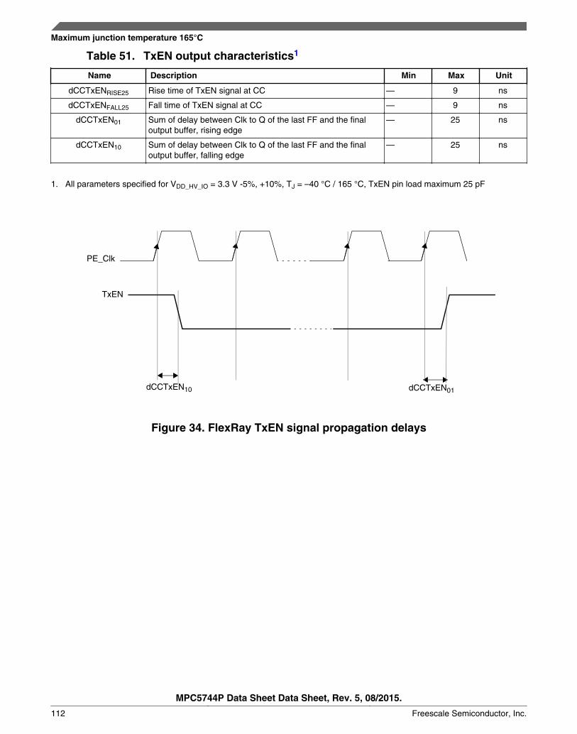
Table 51. TxEN output characteristics1
Name Description Min Max Unit
dCCTxENRISE25 Rise time of TxEN signal at CC — 9 ns
dCCTxENFALL25 Fall time of TxEN signal at CC — 9 ns
dCCTxEN01 Sum of delay between Clk to Q of the last FF and the finaloutput buffer, rising edge
— 25 ns
dCCTxEN10 Sum of delay between Clk to Q of the last FF and the finaloutput buffer, falling edge
— 25 ns
1. All parameters specified for VDD_HV_IO = 3.3 V -5%, +10%, TJ = –40 °C / 165 °C, TxEN pin load maximum 25 pF
dCCTxEN10 dCCTxEN01
TxEN
PE_Clk
Figure 34. FlexRay TxEN signal propagation delays
Maximum junction temperature 165°C
MPC5744P Data Sheet Data Sheet, Rev. 5, 08/2015.
112 Freescale Semiconductor, Inc.

3.19.7.3 TxD
dCCTxD50%
TxD
dCCTxDFALL dCCTxDRISE
20 %
50 %
80 %
Figure 35. FlexRay TxD signal
Table 52. TxD output characteristics
Name Description1 Min Max Unit
dCCTxAsym Asymmetry of sending CC @ 25 pF load
(=dCCTxD50% - 100 ns)
–2.45 2.45 ns
dCCTxDRISE25+dCCTxDFALL25
Sum of Rise and Fall time of TxD signal at the output — 9 ns
dCCTxD01 Sum of delay between Clk to Q of the last FF and the finaloutput buffer, rising edge
— 25 ns
dCCTxD10 Sum of delay between Clk to Q of the last FF and the finaloutput buffer, falling edge
— 25 ns
1. All parameters specified for VDD_HV_IO = 3.3 V -5%, +10%, TJ = –40 °C / 165 °C, TxD pin load maximum 25 pF
Maximum junction temperature 165°C
MPC5744P Data Sheet Data Sheet, Rev. 5, 08/2015.
Freescale Semiconductor, Inc. 113

dCCTxD10 dCCTxD01
TxD
PE_Clk*
*FlexRay Protocol Engine Clock
Figure 36. FlexRay TxD signal propagation delays
3.19.7.4 RxDTable 53. RxD input characteristic
Name Description1 Min Max Unit
C_CCRxD Input capacitance on RxD pin — 7 pF
uCCLogic_1 Threshold for detecting logic high 35 70 %
uCCLogic_0 Threshold for detecting logic low 30 65 %
dCCRxD01 Sum of delay from actual input to the Dinput of the first FF, rising edge
— 10 ns
dCCRxD10 Sum of delay from actual input to the Dinput of the first FF, falling edge
— 10 ns
1. All parameters specified for VDD_HV_IO = 3.3 V -5%, +10%, TJ = –40 / 165 °C
3.19.7.5 Receiver asymmetryTable 54. Receiver asymmetry
Name Description Min Max Unit
dCCRxAsymAccept15 Acceptance of asymmetry at receiving CC with 15 pF load (*) –31.5 +44.0 ns
dCCRxAsymAccept25 Acceptance of asymmetry at receiving CC with 25 pF load (*) –30.5 +43.0 ns
Maximum junction temperature 165°C
MPC5744P Data Sheet Data Sheet, Rev. 5, 08/2015.
114 Freescale Semiconductor, Inc.

3.19.8 Ethernet switching specifications
The following timing specs are defined at the chip I/O pin and must be translatedappropriately to arrive at timing specs/constraints for the physical interface.
3.19.8.1 MII signal switching specifications
The following timing specs meet the requirements for MII style interfaces for a range oftransceiver devices.
Table 55. MII signal switching specifications
Symbol Description Min. Max. Unit
— RXCLK frequency — 25 MHz
MII1 RXCLK pulse width high 35% 65% RXCLK
period
MII2 RXCLK pulse width low 35% 65% RXCLK
period
MII3 RXD[3:0], RXDV, RXER to RXCLK setup 5 — ns
MII4 RXCLK to RXD[3:0], RXDV, RXER hold 5 — ns
— TXCLK frequency — 25 MHz
MII5 TXCLK pulse width high 35% 65% TXCLK
period
MII6 TXCLK pulse width low 35% 65% TXCLK
period
MII7 TXCLK to TXD[3:0], TXEN, TXER invalid 2 — ns
MII8 TXCLK to TXD[3:0], TXEN, TXER valid — 25 ns
MII7MII8
Valid data
Valid data
Valid data
MII6 MII5
TXCLK (input)
TXD[n:0]
TXEN
TXER
Figure 37. RMII/MII transmit signal timing diagram
Maximum junction temperature 165°C
MPC5744P Data Sheet Data Sheet, Rev. 5, 08/2015.
Freescale Semiconductor, Inc. 115

MII2 MII1
MII4MII3
Valid data
Valid data
Valid data
RXCLK (input)
RXD[n:0]
RXDV
RXER
Figure 38. RMII/MII receive signal timing diagram
3.19.8.2 RMII signal switching specifications
The following timing specs meet the requirements for RMII style interfaces for a range oftransceiver devices.
Table 56. RMII signal switching specifications
Num Description Min. Max. Unit
— EXTAL frequency (RMII input clock RMII_CLK) — 50 MHz
RMII1 RMII_CLK pulse width high 35% 65% RMII_CLKperiod
RMII2 RMII_CLK pulse width low 35% 65% RMII_CLKperiod
RMII3 RXD[1:0], CRS_DV, RXER to RMII_CLK setup 4 — ns
RMII4 RMII_CLK to RXD[1:0], CRS_DV, RXER hold 2 — ns
RMII7 RMII_CLK to TXD[1:0], TXEN invalid 4 — ns
RMII8 RMII_CLK to TXD[1:0], TXEN valid — 15 ns
4 Obtaining package dimensionsPackage dimensions are provided in package drawings.
To find a package drawing, go to http://www.freescale.com and perform a keywordsearch for the drawing’s document number:
If you want the drawing for this package Then use this document number
144-pin LQFP 98ASS23177W
257-ball MAPBGA 98ASA00081D
Obtaining package dimensions
MPC5744P Data Sheet Data Sheet, Rev. 5, 08/2015.
116 Freescale Semiconductor, Inc.

5 Ordering information5744PM PC LQ
Note: Not all options are available on all devices.
K0Qualification status
Core code (Power Architecture) Device number
Fab and mask identifier
Package identifier
Tape and reel status
Temperature range
M = –40°C to +125°C
Package identifier
LQ = 144 LQFP
Qualification status
P = Pre-qualification
Tape and reel status
R = Tape and reel (blank) = Trays
K
Temperature range
MM = 257 MAPBGA
R
M = Fully spec. qualified, general market flow S = Fully spec. qualified, automotive flow 5 = 150 MHz K = –40°C to +135°C
for extended temp (+165°C TJ)
G
E = Ethernet F = FlexRay
G = both (blank) = neither
9
Operating frequency
Operating frequency
9 = 200 MHz 8 = 180 MHz
Table 57. Orderable part number examples
Part number1 Flash/SRAM Package Other features
SPC5744PFK1MLQ9 2.5 MB/384 KB 144 LQFP (Pb free) -40 to +125 °C
SPC5744PGK1MMM9 2.5 MB/384 KB 257 MAPBGA (Pb free) Ethernet interface
LFAST interface
Nexus Aurora
-40 to +125 °C
SPC5743PFK1MLQ9 2 MB/256 KB 144 LQFP (Pb free) -40 to +125 °C
SPC5743PGK1MMM9 2 MB/256 KB 257 MAPBGA (Pb free) Ethernet interface
LFAST interface
Nexus Aurora
-40 to +125 °C
SPC5742PFK1MLQ9 1.5 MB/192 KB 144 LQFP (Pb free) -40 to +125 °C
SPC5742PGK1MMM9 1.5 MB/192 KB 257 MAPBGA (Pb free) Ethernet interface
LFAST interface
Nexus Aurora
-40 to +125 °C
SPC5741PFK1MLQ9 1 MB/128 KB 144 LQFP (Pb free) -40 to +125 °C
SPC5741PGK1MMM9 1 MB/128 KB 257 MAPBGA (Pb free) Ethernet interface
LFAST interface
Nexus Aurora
-40 to +125 °C
Ordering information
MPC5744P Data Sheet Data Sheet, Rev. 5, 08/2015.
Freescale Semiconductor, Inc. 117

1. All packaged devices are PPC, rather than MPC or SPC, until product qualifications are complete. Not all configurationsare available in the PPC parts.
6 Document revision historyThe following table summarizes revisions to this document since the previous release.
Table 58. Revision history
Revision Date Description of changes
5 08/2015 Recommended operating conditions• In Table 13 existing row for VDD_LV_COR, added a footnote "The chip functions down to the
point where LVD_CORE or up to the point where HVD_CORE resets the chip by default."
RESET sequence duration• In Table 38 existing row for TDRB, typical value removed and max value changed from 14 to
18 ms.• In Table 38 existing row for TERLB, typical value removed and max value changed from 13.5 to
17.5 ms.
ADC electrical characteristics• Added a note: "The ADC performance specifications are not guaranteed if two ADCs
simultaneously sample the same shared channel".
16 MHz Internal RC Oscillator (IRCOSC) electrical specifications• In Table 26 existing row δFvar_noT added a footnote: "The typical user trim step size
(dfTRIM) ........on characterization results."
Reset pad (EXT_POR, RESET) electrical characteristics• Updated Figure 9 and Figure 10• Updated Table 40 and seperated EXT_POR electrical specifications into new Table 41• Added Table 41 for EXT_POR electrical specifications.
DC electrical characteristics• In Table 20 updated LV (core) Supply Voltage to 1.19 volts
Voltage regulator electrical characteristics• In Table 17 existing row "supply ramp rate" max value is changed from 1 V/ms to 0.125 V/µs.
LVDS pins/balls• Deleted "Debug LFAST" from foot note 1 in Table 6
Generic pins/balls• In Table 8
• Signal description of port pin I[5] is changed from "LFAST PLL Phase 0 clock onnegative terminal" to "SIPI/LFAST PLL Phase 0 clock on negative terminal".
• Signal description of port pin C[12] is changed from "LFAST PLL Phase 0 clock onpositive terminal" to "SIPI/LFAST PLL Phase 0 clock on positive terminal".
Document revision history
MPC5744P Data Sheet Data Sheet, Rev. 5, 08/2015.
118 Freescale Semiconductor, Inc.

How to Reach Us:
Home Page:freescale.com
Web Support:freescale.com/support
Information in this document is provided solely to enable system andsoftware implementers to use Freescale products. There are no expressor implied copyright licenses granted hereunder to design or fabricateany integrated circuits based on the information in this document.Freescale reserves the right to make changes without further notice toany products herein.
Freescale makes no warranty, representation, or guarantee regardingthe suitability of its products for any particular purpose, nor doesFreescale assume any liability arising out of the application or use ofany product or circuit, and specifically disclaims any and all liability,including without limitation consequential or incidental damages.“Typical” parameters that may be provided in Freescale data sheetsand/or specifications can and do vary in different applications, andactual performance may vary over time. All operating parameters,including “typicals,” must be validated for each customer application bycustomer's technical experts. Freescale does not convey any licenseunder its patent rights nor the rights of others. Freescale sells productspursuant to standard terms and conditions of sale, which can be foundat the following address: freescale.com/SalesTermsandConditions.
Freescale, the Freescale logo, SafeAssure, and the SafeAssure logoare trademarks of Freescale Semiconductor, Inc., Reg. U.S. Pat. & Tm.Off. All other product or service names are the property of theirrespective owners. The Power Architecture and Power.org logos andrelated marks are trademarks and service marks licensed by Power.org.
© 2011–2015 Freescale Semiconductor, Inc.
Document Number MPC5744PRevision 5, 08/2015