Embed Size (px)
Citation preview
Freescale Semiconductor Document Number:AN4939
Application Note Rev 0, 04/2014
MPC5744P Software Start Up andOptimizationby: Jamaal Fraser
1 IntroductionThis application note describes a recommended software start up procedure for the MPC5744P 32-bit Power Architecture® automotive microcontroller. This covers starting the Power Architecture core, memory protection unit (MPU), clock frequency (PLL), watchdog timer, flash memory controller, and internal static RAM. Recommended configuration settings for these modules will be given for the purpose of optimizing system performance.
The MPC5744P is a 32-bit Power Architecture Microcontroller that targets chassis and safety applications and other applications requiring a high Automotive Safety Integrity Level (SIL). The host processor core of the MPC5744P is a CPU from the e200 family of compatible Power Architecture cores. The z425n3 dual issue core provides very high efficiency— high performance with minimum power dissipation—and operates at a maximum frequency of 200MHz. The processor family implements low-cost versions of the PowerISA 2.06 architecture. An Embedded Floating-point (EFPU2) Auxiliary Processing Unit (APU) is provided to support real-time single-precision embedded numeric operations using the general purpose registers (GPRs). A Lightweight Signal Processing Extension (LSP) APU is provided to support real-time SIMD fixed-point embedded numerics operations using the GPRs. All arithmetic instructions that execute in the core operate on data in the GPRs. The z425n3 core implements the VLE (variable-length encoding) ISA, providing improved code density. The VLE
© 2014 Freescale Semiconductor, Inc.
Contents
1 Introduction..............................................................1
2 Overview...................................................................2
3 Startup code..............................................................2
4 MCU optimization..................................................15
5 Conclusion...............................................................17
A Code.......................................................................17
ISA is documented in PowerISA 2.06, a separate document. Note that the base PowerISA 2.06 fixed-length 32-bit instructionset is not directly supported.
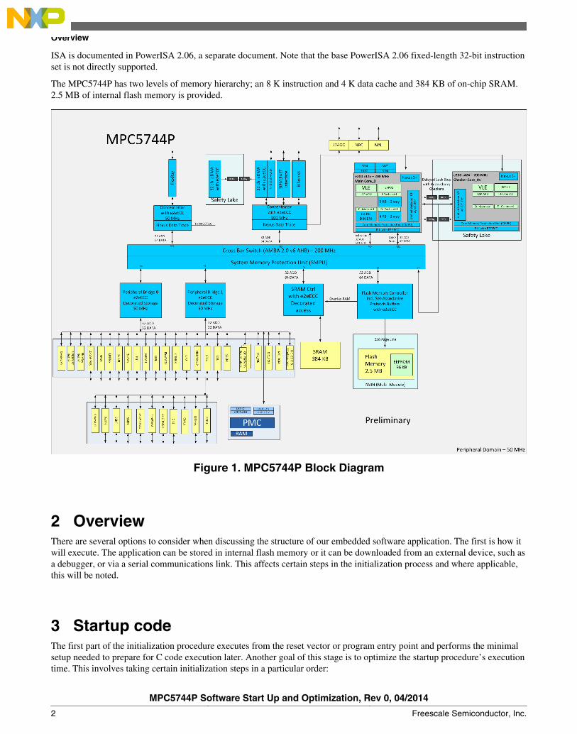
The MPC5744P has two levels of memory hierarchy; an 8 K instruction and 4 K data cache and 384 KB of on-chip SRAM.2.5 MB of internal flash memory is provided.
Figure 1. MPC5744P Block Diagram
2 OverviewThere are several options to consider when discussing the structure of our embedded software application. The first is how itwill execute. The application can be stored in internal flash memory or it can be downloaded from an external device, such asa debugger, or via a serial communications link. This affects certain steps in the initialization process and where applicable,this will be noted.
3 Startup codeThe first part of the initialization procedure executes from the reset vector or program entry point and performs the minimalsetup needed to prepare for C code execution later. Another goal of this stage is to optimize the startup procedure’s executiontime. This involves taking certain initialization steps in a particular order:
Overview
MPC5744P Software Start Up and Optimization, Rev 0, 04/2014
2 Freescale Semiconductor, Inc.
1. Reset configuration2. Initialize the core registers3. Disable the watchdog timer4. Program PLL5. Initialize SRAM6. Configure core memory protection unit7. Enable instruction and data caches8. Initialize C runtime environment
3.1 Reset configurationThere are several ways to begin software execution after device reset. These are controlled by external pins and device status.The following sequence applies:
• If the FAB (Force Alternate Boot Mode) pin is set to boot in serial mode the device can be forced into an AlternateBoot Loader Mode. The type of alternate boot mode is selected according to the ABS (Alternate Boot Selector) pinsand is controlled by the Boot Access Module (BAM).See Table 1
• If FAB is not set the System Status and Configuration Module (SSCM) searches the flash and attempts to identify aflash memory sector with a valid boot signature.
• If none of the flash memory sectors contains a valid boot signature, the device will go into static mode. Static modemeans the device enters the low power mode SAFE and the processor executes a wait instruction.
Table 1. Hardware Configuration
FAB ABS Standby-RAMBootFlag
Boot ID Boot Mode
1 00 0 - Serial Boot SCI
1 01 0 - Serial Boot CAN
0 - 0 valid Single Chip
0 - 0 not found Static Mode
When using a hardware debugger connected via the JTAG or Nexus ports, the standard boot process can be bypassed. Thedebugger can download software to RAM or Flash via the debug interface and specify a start location for execution. In thiscase, much of the low-level device initialization is accomplished by the debugger using configuration scripts.
This application note will focus on the internal flash boot case because it performs all initialization tasks explicitly in theapplication code. During any power-on, external, or internal reset event, except for software reset, the SSCM begins bysearching for a valid Reset Configuration Half Word (RCHW) in internal flash memory at one of the following pre-definedaddresses defined in Table 2
Table 2. Possible RCHW locations in the internal flash
Boot Search Order Address Block Size
1st 0x00F9_8000 16 K
2nd 0x00F9_C000 16 K
3rd 0x00FA_0000 64 K
4th 0x00FB_0000 64 K
5th 0x0100_0000 256 K
6th 0x0104_0000 256 K
Table continues on the next page...
Startup code
MPC5744P Software Start Up and Optimization, Rev 0, 04/2014
Freescale Semiconductor, Inc. 3
Table 2. Possible RCHW locations in the internal flash (continued)
Boot Search Order Address Block Size
7th 0x0108_0000 256 K
8th 0x010C_0000 256 K
The RCHW is a collection of control bits that specify a minimal MCU configuration after reset. If a valid RCHW is notfound the MCU will enter Static mode. See Table 3 below for the format for the RCHW:
Table 3. Reset configuration half word
0 1 2 3 4 5 6 7 8 9 10 11 12 13 14 15
0 0 0 0 0 0 0 VLE Boot Identifier
Reserved 1 0 1 0 1 1 0 1 0
The RCHW occupies the most significant 16 bits of the first 32-bit internal memory word at the boot location. The next 32bits contain the boot vector address. After applying the RCHW, the SSCM will branch to this boot vector. During softwareinitialization, reserve space for both of these 32-bit locations in the linker directive file as follows:
MEMORY{ flash_rcw : org = FLASH_BASE_ADDR, len = 0x8 …}
SECTIONS{ .rcw : {} > flash_rcw …}
In the initialization code file, these two locations are generated with a valid RCHW encoding and the start address symbol forcode entry point.
.section .rcw .LONG 0x015A0000 # RCHW .LONG _start # Code entry point
When debugging, the RCHW is not applied when the SSCM does not execute.
3.2 Initialize Core RegistersThe MPC5744P's core needs its registers initialized before they are used otherwise the two cores will contain differentrandom data. If this is the case when a value is stored to memory (e.g. stacked) it will cause a Lock Step error.
#-------------------------------------------------------# # Initialize Core Registers # #-------------------------------------------------------# # GPR's 0-31 e_li r0, 0 e_li r1, 0 e_li r2, 0 e_li r3, 0 e_li r4, 0 e_li r5, 0 e_li r6, 0 e_li r7, 0
Startup code
MPC5744P Software Start Up and Optimization, Rev 0, 04/2014
4 Freescale Semiconductor, Inc.
e_li r8, 0 e_li r9, 0 e_li r10, 0 e_li r11, 0 e_li r12, 0 e_li r13, 0 e_li r14, 0 e_li r15, 0 e_li r16, 0 e_li r17, 0 e_li r18, 0 e_li r19, 0 e_li r20, 0 e_li r21, 0 e_li r22, 0 e_li r23, 0 e_li r24, 0 e_li r25, 0 e_li r26, 0 e_li r27, 0 e_li r28, 0 e_li r29, 0 e_li r30, 0 e_li r31, 0
# Init any other CPU register which might be stacked (before being used).
mtspr 1, r1 # XER mtcrf 0xFF, r1 mtspr CTR, r1 mtspr SPRG0, r1 mtspr SPRG1, r1 mtspr SPRG2, r1 mtspr SPRG3, r1 mtspr SRR0, r1 mtspr SRR1, r1 mtspr CSRR0, r1 mtspr CSRR1, r1 mtspr MCSRR0, r1 mtspr MCSRR1, r1 mtspr DEAR, r1 mtspr IVPR, r1 mtspr USPRG0, r1 mtspr 62, r1 # ESR mtspr 8,r31 # LR
3.3 WatchdogIn this example the Software Watchdog Timer (SWT) is disabled so that it does not interfere with application debug sessionsIf the SWT is enabled, there may be points within the initialization procedure that require watchdog service, depending onthe timeout period of the watchdog.
#************************ Disable Software Watchdog (SWT) ***************** e_lis r4, 0xFC05 e_or2i r4, 0x0000
e_li r3, 0xC520 e_stw r3, 0x10(r4)
e_li r3, 0xD928 e_stw r3, 0x10(r4)
e_lis r3, 0xFF00
Startup code
MPC5744P Software Start Up and Optimization, Rev 0, 04/2014
Freescale Semiconductor, Inc. 5
e_or2i r3, 0x010A e_stw r3, 0(r4)
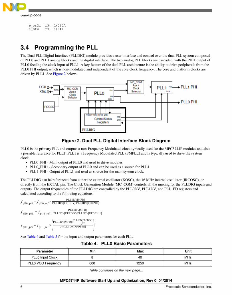
3.4 Programming the PLLThe Dual PLL Digital Interface (PLLDIG) module provides a user interface and control over the dual PLL system composedof PLL0 and PLL1 analog blocks and the digital interface. The two analog PLL blocks are cascaded, with the PHI1 output ofPLL0 feeding the clock input of PLL1. A key feature of the dual PLL architecture is the ability to drive peripherals from thePLL0 PHI output, which is non-modulated and independent of the core clock frequency. The core and platform clocks aredriven by PLL1. See Figure 2 below.
Figure 2. Dual PLL Digital Interface Block Diagram
PLL0 is the primary PLL and outputs a non-Frequency Modulated clock typically used for the MPC5744P modules and alsoa possible reference for PLL1. PLL1 is a Frequency Modulated PLL (FMPLL) and is typically used to drive the systemclock.
• PLL0_PHI - Main output of PLL0 and used to drive modules• PLL0_PHI1 - Secondary output of PLL0 and can be used as a source for PLL1• PLL1_PHI - Output of PLL1 and used as source for the main system clock.
The PLLDIG can be referenced from either the external oscillator (XOSC), the 16 MHz internal oscillator (IRCOSC), ordirectly from the EXTAL pin. The Clock Generation Module (MC_CGM) controls all the muxing for the PLLDIG inputs andoutputs. The output frequencies of the PLLDIG are controlled by the PLL0DV, PLL1DV, and PLL1FD registers andcalculated according to the following equations:
See Table 4 and Table 5 for the input and output parameters for each PLL.
Table 4. PLL0 Basic Parameters
Parameter Min Max Unit
PLL0 Input Clock 8 40 MHz
PLL0 VCO Frequency 600 1250 MHz
Table continues on the next page...
Startup code
MPC5744P Software Start Up and Optimization, Rev 0, 04/2014
6 Freescale Semiconductor, Inc.
Table 4. PLL0 Basic Parameters (continued)
Parameter Min Max Unit
PLL0_PHI Frequency 4.76 625 MHz
PLL0_PHI1 Frequency 20 156 MHz
PLL0 Lock Time - 100 μs
Table 5. PLL1 Basic Parameters
Parameter Min Max Unit
PLL1 Input Clock 38 78 MHz
PLL1 VCO Frequency 600 1250 MHz
PLL1_PHI Frequency 4.76 625 MHz
PLL1 Lock Time - 100 μs
For maximum performance it is typical to set the outputs as follows:
• PLL0_PHI = 160 MHz• PLL0_PHI1 = 40 MHz• PLL1_PHI = 200 MHz
See Table 6 for some example values for the different bit fields of the PLL0DV, PLL1DV, and PLL1FD registers to achievethese frequencies.
Table 6. Example PLL settings
Reference Clock PREDIV MFD RFDPHI FRCDIV
40 MHz XOSC PLL0_PHI1 8
2 na
40 MHz XOSC PLL0_PHI1 8 na
40 MHz XOSC PLL1_PHI na 20 2 0
Coming out of reset PLL0 and PLL1 are disabled per the DRUN mode configuration. The following is the procedure toinitialize the PLLDIG.
1. Configure PLL0a. With PLL0 disabled, program PLL0 clock sourceb. Program appropriate values to the PLL0DV registerc. Turn on XOSC and PLL0d. Wait for mode transition to complete
2. Configure PLL1a. With PLL1 disabled, program PLL1 clock sourceb. Program appropriate value to the PLL1DV registerc. Turn on PLL1d. Wait for mode transition to complete
The following example sets up the PLLDIG to produce the clocks as described above.
#******************************** Program PLL ***************************** # Program PLL0 clock source e_lis r5, 0xFFFB # MC_CGM.AC3_SC address
Startup code
MPC5744P Software Start Up and Optimization, Rev 0, 04/2014
Freescale Semiconductor, Inc. 7
e_or2i r5, 0x0860
e_lis r4, 0x0100 # SELCTL=1, XOSC source of PLL0 e_or2i r4, 0x0000 e_stw r4, 0x0(r5) # Store MC_CGM.AC3_SC
# Program PLL1 clock course e_lis r4, 0x0100 # SELCTL=1, XOSC source for PLL1 e_or2i r4, 0x0000 e_stw r4, 0x20(r5) # Store MC_CGM.AC4_SC # Program PLL0 settings e_lis r3, 0xFFFB # PLLDIG base address e_or2i r3, 0x0100 e_lis r4, 0x4002 # RFDPHI1=8, PFDPHI=2 e_or2i r4, 0x1008 # PREDIV=1, MFD=8 e_stw r4, 0x8(r3) # Store PLLDIG.PLL0DV # Enable XOSC and PLL0 e_lis r5, 0xFFFB # MC_ME base address e_or2i r5, 0x8000 e_lis r4, 0x0013 # Enable XOSC and PLL0 in DRUN mode and e_or2i r4, 0x0072 # select PLL0 as SYS_CLK e_stw r4, 0x2C(r5) # Store MC_ME.DRUN_MC.R e_lis r6, 0x3000 # Load Mode & Key e_or2i r6, 0x5AF0 e_lis r7, 0x3000 # Load Mode & Key inverted e_or2i r7, 0xA50F e_stw r6, 4(r5) # Store MC_ME.MCTL.R e_stw r7, 4(r5) # Store MC_ME.MCTL.R e_lis r24, 0x0800 # Load mask for MC_ME.GS.MTRANS e_lis r25, 0x3000 # Load mask for MC_ME.GS.S_CURRENT_MODE mode_trans0: e_lwz r4, 0(r5) # Load MC_ME.GS register se_and. r24, r4 # M_TRANS=0, transition complete e_bne mode_trans0 se_and. r25, r4 # Check that are in DRUN mode e_beq mode_trans0 # Program PLL1 settings e_lis r4, 0x0002 # RFDPHI=2 e_or2i r4, 0x0014 # MFD=20 e_stw r4, 0x28(r3) # Store PLLDIG.PLL1DV # Enable PLL1 and select as SYS_CLK e_lis r4, 0x0013 # Enable PLL1 in DRUN mode and e_or2i r4, 0x00F4 # select PLL1 as SYS_CLK e_stw r4, 0x2C(r5) # Store MC_ME.DRUN_MC.R e_lis r6, 0x3000 # Load Mode & Key e_or2i r6, 0x5AF0
e_lis r7, 0x3000 # Load Mode & Key inverted e_or2i r7, 0xA50F e_stw r6, 4(r5) # Store MC_ME.MCTL.R e_stw r7, 4(r5) # Store MC_ME.MCTL.R
Startup code
MPC5744P Software Start Up and Optimization, Rev 0, 04/2014
8 Freescale Semiconductor, Inc.
e_lis r24, 0x0800 # Load mask for MC_ME.GS.MTRANS e_lis r25, 0x3000 # Load mask for MC_ME.GS.S_CURRENT_MODE mode_trans1: e_lwz r4, 0(r5) # Load MC_ME.GS register se_and. r24, r4 # M_TRANS=0. transition complete e_bne mode_trans1 se_and. r25, r4 # Check that are in DRUN mode e_beq mode_trans1
3.5 Memory protection unit (MPU)The core MPU has the following features:
• 24 entry region descriptor table with support for 6 arbitrary-sized instruction memory regions, 12 arbitrary-sized datamemory regions, and 6 additional arbitrary-sized regions programmable as instruction or data memory regions
• Region 0-5 instruction, 6-17 data, and 18-23 shared.• Ability to set access permissions and memory attributes on a per-region basis• Process ID aware, with per-bit masking of TID values• Capability for masking upper address bits in the range comparison• Capability of bypassing permissions for checking for selected access types• Per-entry write-once logic for entry protection• Hardware flash invalidation support and per-entry invalidation protection controls• Ability to optionally utilize region descriptors for generating debug events and watchpoints• Software managed by mpure and mpuwe instructions
The core MPU is disabled by default and can be left disabled if the user chooses. It is important to remember that once thecore MPU has been enabled that any access made will be checked against the region table unless MPU protections arebypassed for that access type in the MPU0CSR0 register. Please see the MPC5744P Reference Manual for more details.
See Table 7 for how the software sets up the core Memory Protection Unit (MPU).
Table 7. MMU Configuration
Region Description Address Size Attributes
0 Flash - Instruction 0x0040_0000 28 MB User & Supervisor Read, Write, Execute. Cacheable
1 SRAM - Instruction 0x4000_0000 384 KB User & Supervisor Read, Write, Execute. Cacheable
6 SRAM - Data 0x4000_0000 384 KB User & Supervisor Read, Write, Execute. Cacheable
7 Flash - Data 0x0040_0000 28 MB User & Supervisor Read, Write, Execute. Cacheable
8 P_BRIDGE 1/0 -Data
0xF800_0000 128 MB User & Supervisor Read, Write, Execute. Non-Cacheable,Guarded
There is a region set up to cover any type of access that the software will make once the MPU is enabled. This code isprovided as an example on how to set up the core MPU.
#**************************** Configure Core MPU **************************
# Region 0 (Instruction): Internal Flash @ 0x0040_0000-0x01FF_FFFF e_lis r3, 0xA100 # VALID=1, INST=1, SHD=0, ESEL=0 e_or2i r3, 0x0F00 # UW=1, SW=1, UX/UR=1, SX/SR=1, Cacheable mtspr mas0, r3 e_lis r3, 0x0000 e_or2i r3, 0x0000 mtspr mas1, r3 # TID=0, global e_lis r3, 0x01FF e_or2i r3, 0xFFFF
Startup code
MPC5744P Software Start Up and Optimization, Rev 0, 04/2014
Freescale Semiconductor, Inc. 9
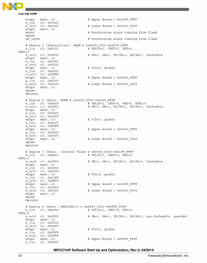
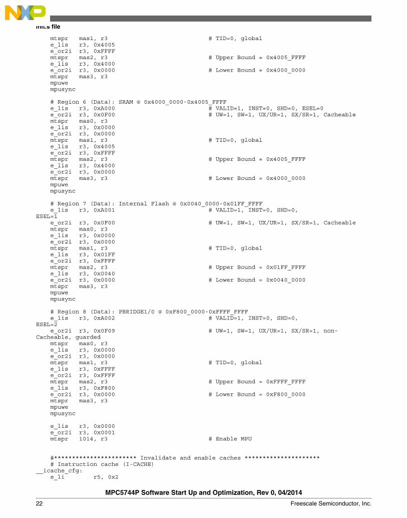
mtspr mas2, r3 # Upper Bound = 0x01FF_FFFF e_lis r3, 0x0040 e_or2i r3, 0x0000 # Lower Bound = 0x0040_0000 mtspr mas3, r3 msync # Synchronize since running from flash mpuwe se_isync # Synchronize since running from flash # Region 1 (Instruction): SRAM @ 0x4000_0000-0x4005_FFFF e_lis r3, 0xA101 # VALID=1, INST=1, SHD=0, ESEL=1 e_or2i r3, 0x0F00 # UW=1, SW=1, UX/UR=1, SX/SR=1, Cacheable mtspr mas0, r3 e_lis r3, 0x0000 e_or2i r3, 0x0000 mtspr mas1, r3 # TID=0, global e_lis r3, 0x4005 e_or2i r3, 0xFFFF mtspr mas2, r3 # Upper Bound = 0x4005_FFFF e_lis r3, 0x4000 e_or2i r3, 0x0000 # Lower Bound = 0x4000_0000 mtspr mas3, r3 mpuwe mpusync # Region 6 (Data): SRAM @ 0x4000_0000-0x4005_FFFF e_lis r3, 0xA000 # VALID=1, INST=0, SHD=0, ESEL=0 e_or2i r3, 0x0F00 # UW=1, SW=1, UX/UR=1, SX/SR=1, Cacheable mtspr mas0, r3 e_lis r3, 0x0000 e_or2i r3, 0x0000 mtspr mas1, r3 # TID=0, global e_lis r3, 0x4005 e_or2i r3, 0xFFFF mtspr mas2, r3 # Upper Bound = 0x4005_FFFF e_lis r3, 0x4000 e_or2i r3, 0x0000 mtspr mas3, r3 # Lower Bound = 0x4000_0000 mpuwe mpusync # Region 7 (Data): Internal Flash @ 0x0040_0000-0x01FF_FFFF e_lis r3, 0xA001 # VALID=1, INST=0, SHD=0, ESEL=1 e_or2i r3, 0x0F00 # UW=1, SW=1, UX/UR=1, SX/SR=1, Cacheable mtspr mas0, r3 e_lis r3, 0x0000 e_or2i r3, 0x0000 mtspr mas1, r3 # TID=0, global e_lis r3, 0x01FF e_or2i r3, 0xFFFF mtspr mas2, r3 # Upper Bound = 0x01FF_FFFF e_lis r3, 0x0040 e_or2i r3, 0x0000 # Lower Bound = 0x0040_0000 mtspr mas3, r3 mpuwe mpusync
# Region 8 (Data): PBRIDGE1/0 @ 0xF800_0000-0xFFFF_FFFF e_lis r3, 0xA002 # VALID=1, INST=0, SHD=0, ESEL=2 e_or2i r3, 0x0F09 # UW=1, SW=1, UX/UR=1, SX/SR=1, non-Cacheable, guarded mtspr mas0, r3 e_lis r3, 0x0000 e_or2i r3, 0x0000 mtspr mas1, r3 # TID=0, global e_lis r3, 0xFFFF e_or2i r3, 0xFFFF mtspr mas2, r3 # Upper Bound = 0xFFFF_FFFF e_lis r3, 0xF800
Startup code
MPC5744P Software Start Up and Optimization, Rev 0, 04/2014
10 Freescale Semiconductor, Inc.
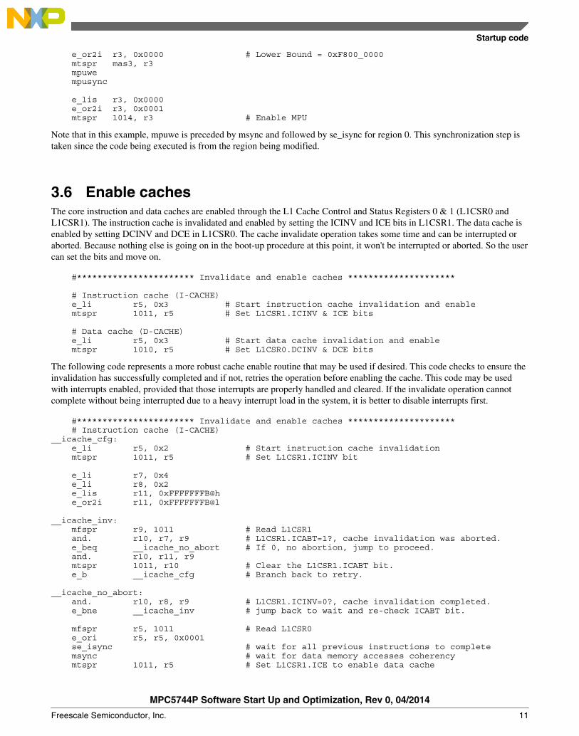
e_or2i r3, 0x0000 # Lower Bound = 0xF800_0000 mtspr mas3, r3 mpuwe mpusync e_lis r3, 0x0000 e_or2i r3, 0x0001 mtspr 1014, r3 # Enable MPU
Note that in this example, mpuwe is preceded by msync and followed by se_isync for region 0. This synchronization step istaken since the code being executed is from the region being modified.
3.6 Enable cachesThe core instruction and data caches are enabled through the L1 Cache Control and Status Registers 0 & 1 (L1CSR0 andL1CSR1). The instruction cache is invalidated and enabled by setting the ICINV and ICE bits in L1CSR1. The data cache isenabled by setting DCINV and DCE in L1CSR0. The cache invalidate operation takes some time and can be interrupted oraborted. Because nothing else is going on in the boot-up procedure at this point, it won't be interrupted or aborted. So the usercan set the bits and move on.
#*********************** Invalidate and enable caches ********************* # Instruction cache (I-CACHE) e_li r5, 0x3 # Start instruction cache invalidation and enable mtspr 1011, r5 # Set L1CSR1.ICINV & ICE bits # Data cache (D-CACHE) e_li r5, 0x3 # Start data cache invalidation and enable mtspr 1010, r5 # Set L1CSR0.DCINV & DCE bits
The following code represents a more robust cache enable routine that may be used if desired. This code checks to ensure theinvalidation has successfully completed and if not, retries the operation before enabling the cache. This code may be usedwith interrupts enabled, provided that those interrupts are properly handled and cleared. If the invalidate operation cannotcomplete without being interrupted due to a heavy interrupt load in the system, it is better to disable interrupts first.
#*********************** Invalidate and enable caches ********************* # Instruction cache (I-CACHE) __icache_cfg: e_li r5, 0x2 # Start instruction cache invalidation mtspr 1011, r5 # Set L1CSR1.ICINV bit
e_li r7, 0x4 e_li r8, 0x2 e_lis r11, 0xFFFFFFFB@h e_or2i r11, 0xFFFFFFFB@l __icache_inv: mfspr r9, 1011 # Read L1CSR1 and. r10, r7, r9 # L1CSR1.ICABT=1?, cache invalidation was aborted. e_beq __icache_no_abort # If 0, no abortion, jump to proceed. and. r10, r11, r9 mtspr 1011, r10 # Clear the L1CSR1.ICABT bit. e_b __icache_cfg # Branch back to retry.
__icache_no_abort: and. r10, r8, r9 # L1CSR1.ICINV=0?, cache invalidation completed. e_bne __icache_inv # jump back to wait and re-check ICABT bit.
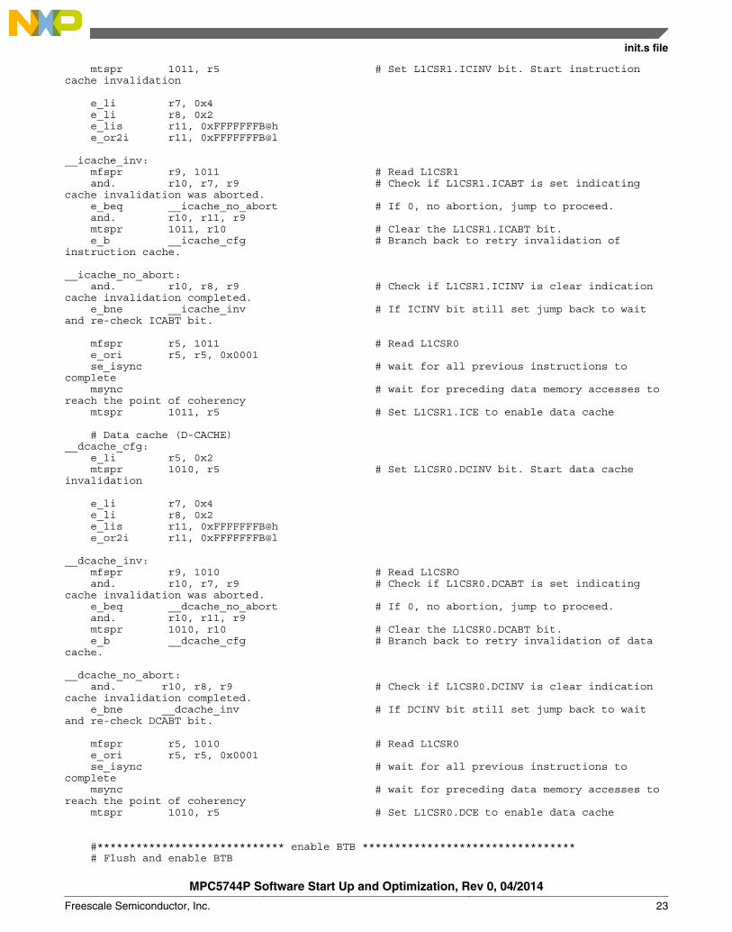
mfspr r5, 1011 # Read L1CSR0 e_ori r5, r5, 0x0001 se_isync # wait for all previous instructions to complete msync # wait for data memory accesses coherency mtspr 1011, r5 # Set L1CSR1.ICE to enable data cache
Startup code
MPC5744P Software Start Up and Optimization, Rev 0, 04/2014
Freescale Semiconductor, Inc. 11
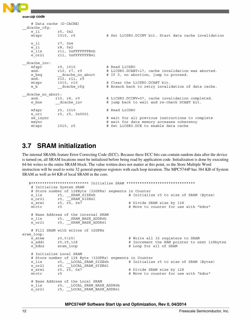
# Data cache (D-CACHE) __dcache_cfg: e_li r5, 0x2 mtspr 1010, r5 # Set L1CSR0.DCINV bit. Start data cache invalidation
e_li r7, 0x4 e_li r8, 0x2 e_lis r11, 0xFFFFFFFB@h e_or2i r11, 0xFFFFFFFB@l
__dcache_inv: mfspr r9, 1010 # Read L1CSRO and. r10, r7, r9 # L1CSR0.DCABT=1?, cache invalidation was aborted. e_beq __dcache_no_abort # If 0, no abortion, jump to proceed. and. r10, r11, r9 mtspr 1010, r10 # Clear the L1CSR0.DCABT bit. e_b __dcache_cfg # Branch back to retry invalidation of data cache.
__dcache_no_abort: and. r10, r8, r9 # L1CSR0.DCINV=0?, cache invalidation completed. e_bne __dcache_inv # jump back to wait and re-check DCABT bit.
mfspr r5, 1010 # Read L1CSR0 e_ori r5, r5, 0x0001 se_isync # wait for all previous instructions to complete msync # wait for data memory accesses coherency mtspr 1010, r5 # Set L1CSR0.DCE to enable data cache
3.7 SRAM initializationThe internal SRAMs feature Error Correcting Code (ECC). Because these ECC bits can contain random data after the deviceis turned on, all SRAM locations must be initialized before being read by application code. Initialization is done by executing64-bit writes to the entire SRAM block. The value written does not matter at this point, so the Store Multiple Wordinstruction will be used to write 32 general-purpose registers with each loop iteration. The MPC5744P has 384 KB of SystemSRAM as well as 64 KB of local SRAM in the core.
#************************** Initialize SRAM ******************************* # Initialize System SRAM # Store number of 128Byte (32GPRs) segments in Counter e_lis r5, __SRAM_SIZE@h # Initialize r5 to size of SRAM (Bytes) e_or2i r5, __SRAM_SIZE@l e_srwi r5, r5, 0x7 # Divide SRAM size by 128 mtctr r5 # Move to counter for use with "bdnz"
# Base Address of the internal SRAM e_lis r5, __SRAM_BASE_ADDR@h e_or2i r5, __SRAM_BASE_ADDR@l
# Fill SRAM with writes of 32GPRs sram_loop: e_stmw r0,0(r5) # Write all 32 registers to SRAM e_addi r5,r5,128 # Increment the RAM pointer to next 128bytes e_bdnz sram_loop # Loop for all of SRAM
# Initialize Local SRAM # Store number of 128 Byte (32GPRs) segments in Counter e_lis r5, __LOCAL_SRAM_SIZE@h # Initialize r5 to size of SRAM (Bytes) e_or2i r5, __LOCAL_SRAM_SIZE@l e_srwi r5, r5, 0x7 # Divide SRAM size by 128 mtctr r5 # Move to counter for use with "bdnz"
# Base Address of the Local SRAM e_lis r5, __LOCAL_SRAM_BASE_ADDR@h e_or2i r5, __LOCAL_SRAM_BASE_ADDR@l
Startup code
MPC5744P Software Start Up and Optimization, Rev 0, 04/2014
12 Freescale Semiconductor, Inc.
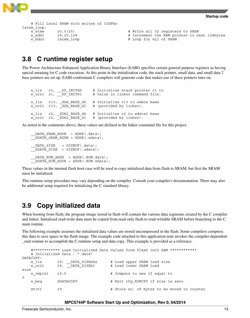
# Fill Local SRAM with writes of 32GPRs lsram_loop: e_stmw r0,0(r5) # Write all 32 registers to SRAM e_addi r5,r5,128 # Increment the RAM pointer to next 128bytes e_bdnz lsram_loop # Loop for all of SRAM
3.8 C runtime register setupThe Power Architecture Enhanced Application Binary Interface (EABI) specifies certain general purpose registers as havingspecial meaning for C code execution. At this point in the initialization code, the stack pointer, small data, and small data 2base pointers are set up. EABI-conformant C compilers will generate code that makes use of these pointers later on.
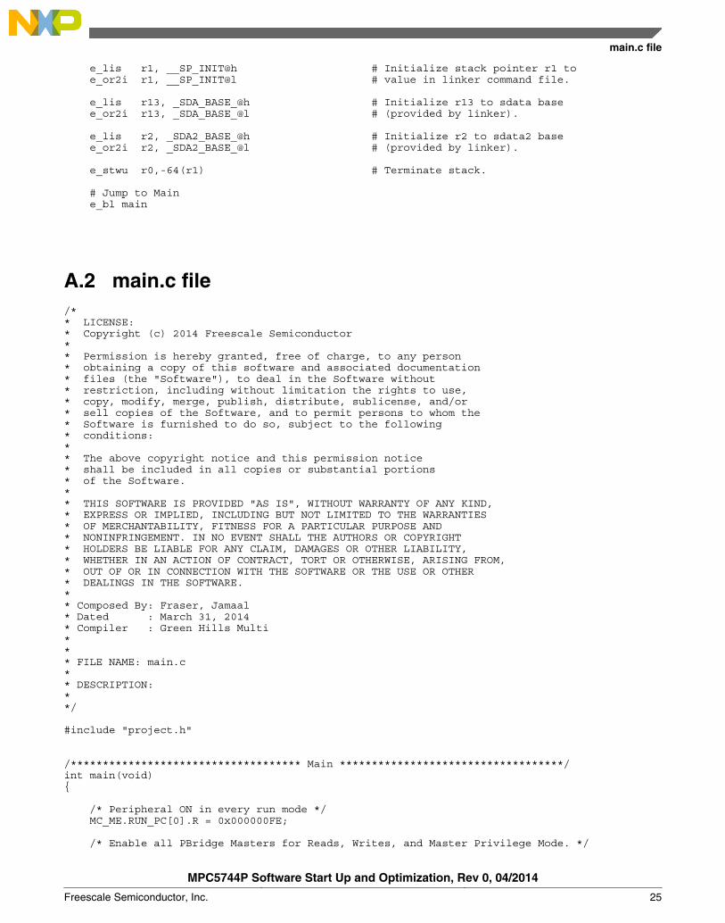
e_lis r1, __SP_INIT@h # Initialize stack pointer r1 to e_or2i r1, __SP_INIT@l # value in linker command file.
e_lis r13, _SDA_BASE_@h # Initialize r13 to sdata base e_or2i r13, _SDA_BASE_@l # (provided by linker).
e_lis r2, _SDA2_BASE_@h # Initialize r2 to sdata2 base e_or2i r2, _SDA2_BASE_@l # (provided by linker).
As noted in the comments above, these values are defined in the linker command file for this project.
__DATA_SRAM_ADDR = ADDR(.data); __SDATA_SRAM_ADDR = ADDR(.sdata);
__DATA_SIZE = SIZEOF(.data); __SDATA_SIZE = SIZEOF(.sdata);
__DATA_ROM_ADDR = ADDR(.ROM.data); __SDATA_ROM_ADDR = ADDR(.ROM.sdata);
These values in the internal flash boot case will be used to copy initialized data from flash to SRAM, but first the SRAMmust be initialized.
This runtime setup procedure may vary depending on the compiler. Consult your compiler's documentation. There may alsobe additional setup required for initializing the C standard library.
3.9 Copy initialized dataWhen booting from flash, the program image stored in flash will contain the various data segments created by the C compilerand linker. Initialized read-write data must be copied from read-only flash to read-writable SRAM before branching to the Cmain routine.
The following example assumes the initialized data values are stored uncompressed in the flash. Some compilers compressthis data to save space in the flash image. The example code attached to this application note invokes the compiler-dependent_start routine to accomplish the C runtime setup and data copy. This example is provided as a reference.
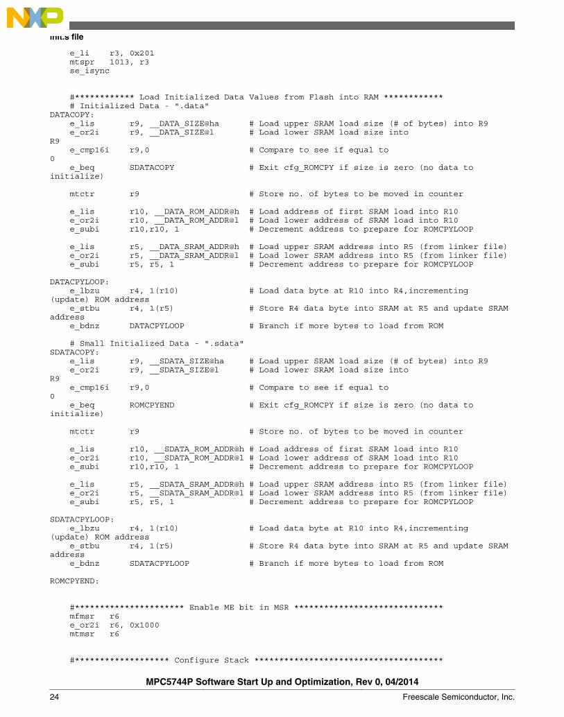
#************ Load Initialized Data Values from Flash into RAM ************ # Initialized Data - ".data"DATACOPY: e_lis r9, __DATA_SIZE@ha # Load upper SRAM load size e_or2i r9, __DATA_SIZE@l # Load lower SRAM load size e_cmp16i r9,0 # Compare to see if equal to 0 e_beq SDATACOPY # Exit cfg_ROMCPY if size is zero mtctr r9 # Store no. of bytes to be moved in counter
Startup code
MPC5744P Software Start Up and Optimization, Rev 0, 04/2014
Freescale Semiconductor, Inc. 13
e_lis r10, __DATA_ROM_ADDR@h # Load address of first SRAM load into R10 e_or2i r10, __DATA_ROM_ADDR@l # Load lower address of SRAM load into R10 e_subi r10,r10, 1 # Decrement address to prepare for ROMCPYLOOP
e_lis r5, __DATA_SRAM_ADDR@h # Load upper SRAM address e_or2i r5, __DATA_SRAM_ADDR@l # Load lower SRAM address e_subi r5, r5, 1 # Decrement address to prepare for ROMCPYLOOP
DATACPYLOOP: e_lbzu r4, 1(r10) # Load data byte, incrementing ROM address e_stbu r4, 1(r5) # Store data byte into SRAM, update SRAM address e_bdnz DATACPYLOOP # Branch if more bytes to load from ROM
# Small Initialized Data - ".sdata" SDATACOPY: e_lis r9, __SDATA_SIZE@ha # Load upper SRAM load size e_or2i r9, __SDATA_SIZE@l # Load lower SRAM load size e_cmp16i r9,0 # Compare to see if equal to 0 e_beq ROMCPYEND # Exit cfg_ROMCPY if size is zero mtctr r9 # Store no. of bytes to be moved in counter e_lis r10, __SDATA_ROM_ADDR@h # Load address of first SRAM load into R10 e_or2i r10, __SDATA_ROM_ADDR@l # Load lower address of SRAM load into R10 e_subi r10,r10, 1 # Decrement address to prepare for ROMCPYLOOP
e_lis r5, __SDATA_SRAM_ADDR@h # Load upper SRAM address into R5 (from linker file) e_or2i r5, __SDATA_SRAM_ADDR@l # Load lower SRAM address into R5 (from linker file) e_subi r5, r5, 1 # Decrement address to prepare for ROMCPYLOOP
SDATACPYLOOP: e_lbzu r4, 1(r10) # Load data byte,incrementing ROM address e_stbu r4, 1(r5) # Store data byte into SRAM, update SRAM address e_bdnz SDATACPYLOOP # Branch if more bytes to load from ROM ROMCPYEND:
3.10 OtherThere are some other important aspects of the MPC5744P SOC that need to be initialized before actual operation can occur.
• Mode Control• Peripheral Bridges
The first to address is the mode control for the device. A detailed description of the features and programming of this moduleare out of the scope of this application note but some basic information and setup is needed. Please see the MPC5744PReference Manual for more information.
The MPC5744P has 10 different modes.
• RESET• DRUN• SAFE• TEST• RUN0...3• HALT0• STOP0
Startup code
MPC5744P Software Start Up and Optimization, Rev 0, 04/2014
14 Freescale Semiconductor, Inc.
The system modes are modes such as RESET, DRUN, SAFE, and TEST. These modes aim to ease the configuration andmonitoring of the system. The user modes are modes such as RUN0…3, HALT0, and STOP0 which can be configured tomeet the application requirements in terms of energy management and available processing power. By default out of reset thedevice will be executing in DRUN mode and all peripherals will be frozen. One register write is necessary to turn on allperipherals for execution.
/* Peripheral ON in every run mode */ MC_ME.RUN_PC[0].R = 0x000000FE;
The other operation involves the Peripheral Bridges (AIPS). The peripheral bridge converts the crossbar switch interface toan interface that can access most of the slave peripherals on the chip. Out of reset only the core is enabled for read and writeaccesses to modules connected to the two peripheral bridges. The following two register writes enable all the peripheralbridge masters; Core, DMA, FlexRay, SIPI, and Ethernet.
/* Enable all PBridge Masters for Reads, Writes, and Master Privilege Mode. */ AIPS_0.MPRA.R = 0x70777700; AIPS_1.MPRA.R = 0x70777700;
4 MCU optimizationIn this section, the following areas for potential optimization will be discussed:
• Flash controller• Branch target buffer• Crossbar switch
4.1 Flash optimizationThe on-chip flash array controller comes out of reset with fail-safe settings. Wait states are set to maximum and performancefeatures like prefetch, read buffering, and pipelining are disabled. Wait states and prefect settings can typically be optimizedbased on the operating frequency using the information specified in the MPC5744P data sheet. Prefetch and read bufferingcan typically be optimized depending on what type of code you are executing out of the flash. The following code can bemodified to select the appropriate value for the flash array’s Platform Flash Configuration Register 1 (PFLASH_PFCR1).
The following example is for the 200 MHz operating settings and accomplish the following optimizations:
• Enable line read buffer• Leave read wait states at default value (6) per data sheet recommendation• Enable pipelining with 2 hold cycles between access requests per data sheet recommendation
Since this example is executing from flash memory, you need to load instructions to perform the update of thePFLASH_PFCR1 register into SRAM, and then temporarily execute from there.
#********************* Configure Flash Wait States ************************* # Code is copied to RAM first, then executed, to avoid executing code from flash # while wait states are changing. # Base Address of the internal SRAM e_lis r5, __SRAM_BASE_ADDR@h e_or2i r5, __SRAM_BASE_ADDR@l e_b copy_to_ram
# Settings for SYS_CLK of 200 MHz
MCU optimization
MPC5744P Software Start Up and Optimization, Rev 0, 04/2014
Freescale Semiconductor, Inc. 15
reduce_flash_ws: e_lis r3, 0x0000 # APC=2 pipelined access 2 cycles before prev. data valid e_or2i r3, 0x4601 # RWSC=6 additional wait states, P0_BFEN=1 line buffer enabled e_lis r4, 0xFC03 e_or2i r4, 0x0000 e_stw r3, 0x0(r4) se_isync msync se_blr
copy_to_ram: e_lis r3, reduce_flash_ws@h e_or2i r3, reduce_flash_ws@l e_lis r4, copy_to_ram@h e_or2i r4, copy_to_ram@l subf r4, r3, r4 se_mtctr r4 se_mtlr r5copy: e_lbz r6, 0(r3) e_stb r6, 0(r5) e_addi r3, r3, 1 e_addi r5, r5, 1 e_bdnz copy se_isync msync se_blrl
4.2 Branch target bufferThe MPC5744P Power Architecture cores feature a branch prediction optimization which can be enabled to improve overallperformance by storing the results of branches and using those results to predict the direction of future branches at the samelocation. To initialize the branch target buffer, we need to flash invalidate the buffer and enable branch prediction. This canbe accomplished with a single write to the Branch Unit Control and Status Register (BUCSR).
#***************************** enable BTB ********************************* e_li r3, 0x0201 mtspr 1013, r3 se_isync
NOTEIf the application modifies instruction code in memory after this initialization procedure,the branch target buffer may need to be flushed and re-initialized as it may containbranch prediction for the code that previously existed at the modified locations.
4.3 Crossbar switchIn most cases, the crossbar settings can be left at their reset defaults. Knowing certain things about the application behaviorand use of different masters on the crossbar, it is possible to customize priorities and use algorithms accordingly to obtainsome slight performance improvements. For example, DMA transfers may benefit from a higher priority setting than theCPU load/store when communicating with the peripheral bus. This would prevent DMA transfers from stalling if the CPUwere to poll a status register in a peripheral. However, this is a specific case which may not apply for all applications.
MCU optimization
MPC5744P Software Start Up and Optimization, Rev 0, 04/2014
16 Freescale Semiconductor, Inc.
5 ConclusionThis application note has presented some specific recommendations for initializing this device and optimizing some of thesettings from their reset defaults. This is a starting point only. Other areas to consider include compiler optimization andefficient use of system resources such as DMA and cache. Consult the MPC5744P reference manual for additionalinformation.
Appendix A Code
A.1 init.s file#******************************************************************************# LICENSE:# Copyright (c) 2014 Freescale Semiconductor# # Permission is hereby granted, free of charge, to any person # obtaining a copy of this software and associated documentation # files (the "Software"), to deal in the Software without # restriction, including without limitation the rights to use, # copy, modify, merge, publish, distribute, sublicense, and/or # sell copies of the Software, and to permit persons to whom the # Software is furnished to do so, subject to the following # conditions:# # The above copyright notice and this permission notice # shall be included in all copies or substantial portions # of the Software.# # THIS SOFTWARE IS PROVIDED "AS IS", WITHOUT WARRANTY OF ANY KIND, # EXPRESS OR IMPLIED, INCLUDING BUT NOT LIMITED TO THE WARRANTIES # OF MERCHANTABILITY, FITNESS FOR A PARTICULAR PURPOSE AND # NONINFRINGEMENT. IN NO EVENT SHALL THE AUTHORS OR COPYRIGHT # HOLDERS BE LIABLE FOR ANY CLAIM, DAMAGES OR OTHER LIABILITY, # WHETHER IN AN ACTION OF CONTRACT, TORT OR OTHERWISE, ARISING FROM, # OUT OF OR IN CONNECTION WITH THE SOFTWARE OR THE USE OR OTHER # DEALINGS IN THE SOFTWARE.# # Composed By: Fraser, Jamaal # Dated : March 31, 2014 # Compiler : Green Hills Multi # # # FILE NAME: crt0_core_flash.s # # DESCRIPTION: This is the crt0 file for the core of the MPC5744P MCU ## REV AUTHOR DATE DESCRIPTION OF CHANGE # --- ----------- ---------- --------------------- # 0.1 D.McMenamin 27/Jun/11 Initial Version # 0.2 B.Johnson 19/Jun/12 Modified for Panther # Removed SWT2, SWT1 initialization # 0.3 B.Johnson 02/Dec/12 Changed SWT_CR to enable MAP0 # 0.4 J.Fraser 31/Mar/14 Added MMU and PLL init code and# modified order for optimization in regards# to MPC5744P SW StartUp App. Note.# #******************************************************************************
Conclusion
MPC5744P Software Start Up and Optimization, Rev 0, 04/2014
Freescale Semiconductor, Inc. 17
.globl _start_core #************************** .rcw reset config section ************************* .section .rcw .LONG 0x015A0000 # RCHW.LONG _start_core # Code starts at _start_core#******************************************************************************
.section .init , axv
.vle
.align 4_start_core:
#**************************** Init Core Registers ************************* # The e200z4 core needs its registers initialized before they are used # otherwise in Lock Step mode the two cores will contain different random data. # If this is stored to memory (e.g. stacked) it will cause a Lock Step error.
# GPR's 0-31 e_li r0, 0 e_li r1, 0 e_li r2, 0 e_li r3, 0 e_li r4, 0 e_li r5, 0 e_li r6, 0 e_li r7, 0 e_li r8, 0 e_li r9, 0 e_li r10, 0 e_li r11, 0 e_li r12, 0 e_li r13, 0 e_li r14, 0 e_li r15, 0 e_li r16, 0 e_li r17, 0 e_li r18, 0 e_li r19, 0 e_li r20, 0 e_li r21, 0 e_li r22, 0 e_li r23, 0 e_li r24, 0 e_li r25, 0 e_li r26, 0 e_li r27, 0 e_li r28, 0 e_li r29, 0 e_li r30, 0 e_li r31, 0
# Init any other CPU register which might be stacked (before being used).
mtspr 1, r1 # XER mtcrf 0xFF, r1 mtspr CTR, r1 mtspr SPRG0, r1 mtspr SPRG1, r1 mtspr SPRG2, r1 mtspr SPRG3, r1 mtspr SRR0, r1 mtspr SRR1, r1 mtspr CSRR0, r1 mtspr CSRR1, r1 mtspr MCSRR0, r1 mtspr MCSRR1, r1 mtspr DEAR, r1 mtspr IVPR, r1
init.s file
MPC5744P Software Start Up and Optimization, Rev 0, 04/2014
18 Freescale Semiconductor, Inc.
mtspr USPRG0, r1 mtspr 62, r1 # ESR mtspr 8,r31 # LR
#************************ Disable Software Watchdog (SWT) ***************** e_lis r4, 0xFC05 e_or2i r4, 0x0000
e_li r3, 0xC520 e_stw r3, 0x10(r4)
e_li r3, 0xD928 e_stw r3, 0x10(r4)
e_lis r3, 0xFF00
e_or2i r3, 0x010A e_stw r3, 0(r4) #******************************** Program PLL ***************************** # Program PLL0 clock source e_lis r5, 0xFFFB # MC_CGM.AC3_SC address e_or2i r5, 0x0860
e_lis r4, 0x0100 # SELCTL=1, XOSC source of PLL0 e_or2i r4, 0x0000 e_stw r4, 0x0(r5) # Store MC_CGM.AC3_SC
# Program PLL1 clock course e_lis r4, 0x0100 # SELCTL=1, XOSC source for PLL1 e_or2i r4, 0x0000 e_stw r4, 0x20(r5) # Store MC_CGM.AC4_SC # Program PLL0 settings e_lis r3, 0xFFFB # PLLDIG base address e_or2i r3, 0x0100 e_lis r4, 0x4002 # RFDPHI1=8, PFDPHI=2 e_or2i r4, 0x1008 # PREDIV=1, MFD=8 e_stw r4, 0x8(r3) # Store PLLDIG.PLL0DV # Enable XOSC and PLL0 e_lis r5, 0xFFFB # MC_ME base address e_or2i r5, 0x8000 e_lis r4, 0x0013 # Enable XOSC and PLL0 in DRUN mode and e_or2i r4, 0x0072 # select PLL0 as SYS_CLK e_stw r4, 0x2C(r5) # Store MC_ME.DRUN_MC.R e_lis r6, 0x3000 # Load Mode & Key e_or2i r6, 0x5AF0 e_lis r7, 0x3000 # Load Mode & Key inverted e_or2i r7, 0xA50F e_stw r6, 4(r5) # Store MC_ME.MCTL.R e_stw r7, 4(r5) # Store MC_ME.MCTL.R e_lis r24, 0x0800 # Load mask for MC_ME.GS.MTRANS e_lis r25, 0x3000 # Load mask for MC_ME.GS.S_CURRENT_MODE mode_trans0: e_lwz r4, 0(r5) # Load MC_ME.GS register se_and. r24, r4 # Check M_TRANS bit clear signaling transition complete
init.s file
MPC5744P Software Start Up and Optimization, Rev 0, 04/2014
Freescale Semiconductor, Inc. 19
e_bne mode_trans0 se_and. r25, r4 # Check that are in DRUN mode e_beq mode_trans0 # Program PLL1 settings e_lis r4, 0x0002 # RFDPHI=2 e_or2i r4, 0x0014 # MFD=20 e_stw r4, 0x28(r3) # Store PLLDIG.PLL1DV # Enable PLL1 and select as SYS_CLK e_lis r4, 0x0013 # Enable PLL1 in DRUN mode and e_or2i r4, 0x00F4 # select PLL1 as SYS_CLK e_stw r4, 0x2C(r5) # Store MC_ME.DRUN_MC.R e_lis r6, 0x3000 # Load Mode & Key e_or2i r6, 0x5AF0
e_lis r7, 0x3000 # Load Mode & Key inverted e_or2i r7, 0xA50F e_stw r6, 4(r5) # Store MC_ME.MCTL.R e_stw r7, 4(r5) # Store MC_ME.MCTL.R e_lis r24, 0x0800 # Load mask for MC_ME.GS.MTRANS e_lis r25, 0x3000 # Load mask for MC_ME.GS.S_CURRENT_MODE mode_trans1: e_lwz r4, 0(r5) # Load MC_ME.GS register se_and. r24, r4 # Check M_TRANS bit clear signaling transition complete e_bne mode_trans1 se_and. r25, r4 # Check that are in DRUN mode e_beq mode_trans1 #************************** Initialize SRAM ******************************* # Initialize System SRAM # Store number of 128 Byte (32GPRs) segments in Counter e_lis r5, __SRAM_SIZE@h # Initialize r5 to size of SRAM (Bytes) e_or2i r5, __SRAM_SIZE@l e_srwi r5, r5, 0x7 # Divide SRAM size by 128 mtctr r5 # Move to counter for use with "bdnz"
# Base Address of the internal SRAM e_lis r5, __SRAM_BASE_ADDR@h e_or2i r5, __SRAM_BASE_ADDR@l
# Fill SRAM with writes of 32GPRs sram_loop: e_stmw r0,0(r5) # Write all 32 registers to SRAM e_addi r5,r5,128 # Increment the RAM pointer to next 128bytes e_bdnz sram_loop # Loop for all of SRAM
# Initialize Local SRAM # Store number of 128 Byte (32GPRs) segments in Counter e_lis r5, __LOCAL_SRAM_SIZE@h # Initialize r5 to size of SRAM (Bytes) e_or2i r5, __LOCAL_SRAM_SIZE@l e_srwi r5, r5, 0x7 # Divide SRAM size by 128 mtctr r5 # Move to counter for use with "bdnz"
# Base Address of the Local SRAM e_lis r5, __LOCAL_SRAM_BASE_ADDR@h e_or2i r5, __LOCAL_SRAM_BASE_ADDR@l
# Fill Local SRAM with writes of 32GPRs lsram_loop: e_stmw r0,0(r5) # Write all 32 registers to SRAM e_addi r5,r5,128 # Increment the RAM pointer to next 128bytes e_bdnz lsram_loop # Loop for all of SRAM
init.s file
MPC5744P Software Start Up and Optimization, Rev 0, 04/2014
20 Freescale Semiconductor, Inc.
#********************* Configure Flash Wait States ************************* # Code is copied to RAM first, then executed, to avoid executing code from flash # while wait states are changing. # Base Address of the internal SRAM e_lis r5, __SRAM_BASE_ADDR@h e_or2i r5, __SRAM_BASE_ADDR@l e_b copy_to_ram
# Settings for SYS_CLK of 200 MHzreduce_flash_ws: e_lis r3, 0x0000 # APC=2 pipelined access can be initiated 2 cycles before previous data is valid e_or2i r3, 0x4601 # RWSC=6 additional wait states, , P0_BFEN=1 line buffer enabled e_lis r4, 0xFC03 e_or2i r4, 0x0000 e_stw r3, 0x0(r4) se_isync msync se_blr
copy_to_ram: e_lis r3, reduce_flash_ws@h e_or2i r3, reduce_flash_ws@l e_lis r4, copy_to_ram@h e_or2i r4, copy_to_ram@l subf r4, r3, r4 se_mtctr r4 se_mtlr r5copy: e_lbz r6, 0(r3) e_stb r6, 0(r5) e_addi r3, r3, 1 e_addi r5, r5, 1 e_bdnz copy se_isync msync se_blrl
#**************************** Configure Core MPU ************************** # Region 0 (Instruction): Internal Flash @ 0x0040_0000-0x01FF_FFFF e_lis r3, 0xA100 # VALID=1, INST=1, SHD=0, ESEL=0 e_or2i r3, 0x0F00 # UW=1, SW=1, UX/UR=1, SX/SR=1, Cacheable mtspr mas0, r3 e_lis r3, 0x0000 e_or2i r3, 0x0000 mtspr mas1, r3 # TID=0, global e_lis r3, 0x01FF e_or2i r3, 0xFFFF mtspr mas2, r3 # Upper Bound = 0x01FF_FFFF e_lis r3, 0x0040 e_or2i r3, 0x0000 # Lower Bound = 0x0040_0000 mtspr mas3, r3 msync # Synchronize since running from flash mpuwe se_isync # Synchronize since running from flash # Region 1 (Instruction): SRAM @ 0x4000_0000-0x4005_FFFF e_lis r3, 0xA101 # VALID=1, INST=1, SHD=0, ESEL=1 e_or2i r3, 0x0F00 # UW=1, SW=1, UX/UR=1, SX/SR=1, Cacheable mtspr mas0, r3 e_lis r3, 0x0000 e_or2i r3, 0x0000
init.s file
MPC5744P Software Start Up and Optimization, Rev 0, 04/2014
Freescale Semiconductor, Inc. 21
mtspr mas1, r3 # TID=0, global e_lis r3, 0x4005 e_or2i r3, 0xFFFF mtspr mas2, r3 # Upper Bound = 0x4005_FFFF e_lis r3, 0x4000 e_or2i r3, 0x0000 # Lower Bound = 0x4000_0000 mtspr mas3, r3 mpuwe mpusync # Region 6 (Data): SRAM @ 0x4000_0000-0x4005_FFFF e_lis r3, 0xA000 # VALID=1, INST=0, SHD=0, ESEL=0 e_or2i r3, 0x0F00 # UW=1, SW=1, UX/UR=1, SX/SR=1, Cacheable mtspr mas0, r3 e_lis r3, 0x0000 e_or2i r3, 0x0000 mtspr mas1, r3 # TID=0, global e_lis r3, 0x4005 e_or2i r3, 0xFFFF mtspr mas2, r3 # Upper Bound = 0x4005_FFFF e_lis r3, 0x4000 e_or2i r3, 0x0000 mtspr mas3, r3 # Lower Bound = 0x4000_0000 mpuwe mpusync # Region 7 (Data): Internal Flash @ 0x0040_0000-0x01FF_FFFF e_lis r3, 0xA001 # VALID=1, INST=0, SHD=0, ESEL=1 e_or2i r3, 0x0F00 # UW=1, SW=1, UX/UR=1, SX/SR=1, Cacheable mtspr mas0, r3 e_lis r3, 0x0000 e_or2i r3, 0x0000 mtspr mas1, r3 # TID=0, global e_lis r3, 0x01FF e_or2i r3, 0xFFFF mtspr mas2, r3 # Upper Bound = 0x01FF_FFFF e_lis r3, 0x0040 e_or2i r3, 0x0000 # Lower Bound = 0x0040_0000 mtspr mas3, r3 mpuwe mpusync
# Region 8 (Data): PBRIDGE1/0 @ 0xF800_0000-0xFFFF_FFFF e_lis r3, 0xA002 # VALID=1, INST=0, SHD=0, ESEL=2 e_or2i r3, 0x0F09 # UW=1, SW=1, UX/UR=1, SX/SR=1, non-Cacheable, guarded mtspr mas0, r3 e_lis r3, 0x0000 e_or2i r3, 0x0000 mtspr mas1, r3 # TID=0, global e_lis r3, 0xFFFF e_or2i r3, 0xFFFF mtspr mas2, r3 # Upper Bound = 0xFFFF_FFFF e_lis r3, 0xF800 e_or2i r3, 0x0000 # Lower Bound = 0xF800_0000 mtspr mas3, r3 mpuwe mpusync e_lis r3, 0x0000 e_or2i r3, 0x0001 mtspr 1014, r3 # Enable MPU #*********************** Invalidate and enable caches ********************* # Instruction cache (I-CACHE) __icache_cfg: e_li r5, 0x2
init.s file
MPC5744P Software Start Up and Optimization, Rev 0, 04/2014
22 Freescale Semiconductor, Inc.
mtspr 1011, r5 # Set L1CSR1.ICINV bit. Start instruction cache invalidation
e_li r7, 0x4 e_li r8, 0x2 e_lis r11, 0xFFFFFFFB@h e_or2i r11, 0xFFFFFFFB@l __icache_inv: mfspr r9, 1011 # Read L1CSR1 and. r10, r7, r9 # Check if L1CSR1.ICABT is set indicating cache invalidation was aborted. e_beq __icache_no_abort # If 0, no abortion, jump to proceed. and. r10, r11, r9 mtspr 1011, r10 # Clear the L1CSR1.ICABT bit. e_b __icache_cfg # Branch back to retry invalidation of instruction cache.
__icache_no_abort: and. r10, r8, r9 # Check if L1CSR1.ICINV is clear indication cache invalidation completed. e_bne __icache_inv # If ICINV bit still set jump back to wait and re-check ICABT bit.
mfspr r5, 1011 # Read L1CSR0 e_ori r5, r5, 0x0001 se_isync # wait for all previous instructions to complete msync # wait for preceding data memory accesses to reach the point of coherency mtspr 1011, r5 # Set L1CSR1.ICE to enable data cache
# Data cache (D-CACHE) __dcache_cfg: e_li r5, 0x2 mtspr 1010, r5 # Set L1CSR0.DCINV bit. Start data cache invalidation
e_li r7, 0x4 e_li r8, 0x2 e_lis r11, 0xFFFFFFFB@h e_or2i r11, 0xFFFFFFFB@l
__dcache_inv: mfspr r9, 1010 # Read L1CSRO and. r10, r7, r9 # Check if L1CSR0.DCABT is set indicating cache invalidation was aborted. e_beq __dcache_no_abort # If 0, no abortion, jump to proceed. and. r10, r11, r9 mtspr 1010, r10 # Clear the L1CSR0.DCABT bit. e_b __dcache_cfg # Branch back to retry invalidation of data cache.
__dcache_no_abort: and. r10, r8, r9 # Check if L1CSR0.DCINV is clear indication cache invalidation completed. e_bne __dcache_inv # If DCINV bit still set jump back to wait and re-check DCABT bit.
mfspr r5, 1010 # Read L1CSR0 e_ori r5, r5, 0x0001 se_isync # wait for all previous instructions to complete msync # wait for preceding data memory accesses to reach the point of coherency mtspr 1010, r5 # Set L1CSR0.DCE to enable data cache
#***************************** enable BTB ********************************* # Flush and enable BTB
init.s file
MPC5744P Software Start Up and Optimization, Rev 0, 04/2014
Freescale Semiconductor, Inc. 23
e_li r3, 0x201 mtspr 1013, r3 se_isync #************ Load Initialized Data Values from Flash into RAM ************ # Initialized Data - ".data"DATACOPY: e_lis r9, __DATA_SIZE@ha # Load upper SRAM load size (# of bytes) into R9 e_or2i r9, __DATA_SIZE@l # Load lower SRAM load size into R9 e_cmp16i r9,0 # Compare to see if equal to 0 e_beq SDATACOPY # Exit cfg_ROMCPY if size is zero (no data to initialize) mtctr r9 # Store no. of bytes to be moved in counter e_lis r10, __DATA_ROM_ADDR@h # Load address of first SRAM load into R10 e_or2i r10, __DATA_ROM_ADDR@l # Load lower address of SRAM load into R10 e_subi r10,r10, 1 # Decrement address to prepare for ROMCPYLOOP
e_lis r5, __DATA_SRAM_ADDR@h # Load upper SRAM address into R5 (from linker file) e_or2i r5, __DATA_SRAM_ADDR@l # Load lower SRAM address into R5 (from linker file) e_subi r5, r5, 1 # Decrement address to prepare for ROMCPYLOOP
DATACPYLOOP: e_lbzu r4, 1(r10) # Load data byte at R10 into R4,incrementing (update) ROM address e_stbu r4, 1(r5) # Store R4 data byte into SRAM at R5 and update SRAM address e_bdnz DATACPYLOOP # Branch if more bytes to load from ROM
# Small Initialized Data - ".sdata" SDATACOPY: e_lis r9, __SDATA_SIZE@ha # Load upper SRAM load size (# of bytes) into R9 e_or2i r9, __SDATA_SIZE@l # Load lower SRAM load size into R9 e_cmp16i r9,0 # Compare to see if equal to 0 e_beq ROMCPYEND # Exit cfg_ROMCPY if size is zero (no data to initialize) mtctr r9 # Store no. of bytes to be moved in counter e_lis r10, __SDATA_ROM_ADDR@h # Load address of first SRAM load into R10 e_or2i r10, __SDATA_ROM_ADDR@l # Load lower address of SRAM load into R10 e_subi r10,r10, 1 # Decrement address to prepare for ROMCPYLOOP
e_lis r5, __SDATA_SRAM_ADDR@h # Load upper SRAM address into R5 (from linker file) e_or2i r5, __SDATA_SRAM_ADDR@l # Load lower SRAM address into R5 (from linker file) e_subi r5, r5, 1 # Decrement address to prepare for ROMCPYLOOP
SDATACPYLOOP: e_lbzu r4, 1(r10) # Load data byte at R10 into R4,incrementing (update) ROM address e_stbu r4, 1(r5) # Store R4 data byte into SRAM at R5 and update SRAM address e_bdnz SDATACPYLOOP # Branch if more bytes to load from ROM ROMCPYEND:
#********************** Enable ME bit in MSR ****************************** mfmsr r6 e_or2i r6, 0x1000 mtmsr r6 #******************* Configure Stack **************************************
init.s file
MPC5744P Software Start Up and Optimization, Rev 0, 04/2014
24 Freescale Semiconductor, Inc.
e_lis r1, __SP_INIT@h # Initialize stack pointer r1 to e_or2i r1, __SP_INIT@l # value in linker command file.
e_lis r13, _SDA_BASE_@h # Initialize r13 to sdata base e_or2i r13, _SDA_BASE_@l # (provided by linker).
e_lis r2, _SDA2_BASE_@h # Initialize r2 to sdata2 base e_or2i r2, _SDA2_BASE_@l # (provided by linker).
e_stwu r0,-64(r1) # Terminate stack.
# Jump to Main e_bl main
A.2 main.c file/** LICENSE:* Copyright (c) 2014 Freescale Semiconductor* * Permission is hereby granted, free of charge, to any person * obtaining a copy of this software and associated documentation * files (the "Software"), to deal in the Software without * restriction, including without limitation the rights to use, * copy, modify, merge, publish, distribute, sublicense, and/or * sell copies of the Software, and to permit persons to whom the * Software is furnished to do so, subject to the following * conditions:* * The above copyright notice and this permission notice * shall be included in all copies or substantial portions * of the Software.* * THIS SOFTWARE IS PROVIDED "AS IS", WITHOUT WARRANTY OF ANY KIND, * EXPRESS OR IMPLIED, INCLUDING BUT NOT LIMITED TO THE WARRANTIES * OF MERCHANTABILITY, FITNESS FOR A PARTICULAR PURPOSE AND * NONINFRINGEMENT. IN NO EVENT SHALL THE AUTHORS OR COPYRIGHT * HOLDERS BE LIABLE FOR ANY CLAIM, DAMAGES OR OTHER LIABILITY, * WHETHER IN AN ACTION OF CONTRACT, TORT OR OTHERWISE, ARISING FROM, * OUT OF OR IN CONNECTION WITH THE SOFTWARE OR THE USE OR OTHER * DEALINGS IN THE SOFTWARE.* * Composed By: Fraser, Jamaal * Dated : March 31, 2014 * Compiler : Green Hills Multi * * * FILE NAME: main.c * * DESCRIPTION: * */
#include "project.h"
/************************************ Main ***********************************/int main(void){ /* Peripheral ON in every run mode */ MC_ME.RUN_PC[0].R = 0x000000FE; /* Enable all PBridge Masters for Reads, Writes, and Master Privilege Mode. */
main.c file
MPC5744P Software Start Up and Optimization, Rev 0, 04/2014
Freescale Semiconductor, Inc. 25
AIPS_0.MPRA.R = 0x70777700; AIPS_1.MPRA.R = 0x70777700; while (1); }
A.3 Linker definition file/** LICENSE:* Copyright (c) 2014 Freescale Semiconductor* * Permission is hereby granted, free of charge, to any person * obtaining a copy of this software and associated documentation * files (the "Software"), to deal in the Software without * restriction, including without limitation the rights to use, * copy, modify, merge, publish, distribute, sublicense, and/or * sell copies of the Software, and to permit persons to whom the * Software is furnished to do so, subject to the following * conditions:* * The above copyright notice and this permission notice * shall be included in all copies or substantial portions * of the Software.* * THIS SOFTWARE IS PROVIDED "AS IS", WITHOUT WARRANTY OF ANY KIND, * EXPRESS OR IMPLIED, INCLUDING BUT NOT LIMITED TO THE WARRANTIES * OF MERCHANTABILITY, FITNESS FOR A PARTICULAR PURPOSE AND * NONINFRINGEMENT. IN NO EVENT SHALL THE AUTHORS OR COPYRIGHT * HOLDERS BE LIABLE FOR ANY CLAIM, DAMAGES OR OTHER LIABILITY, * WHETHER IN AN ACTION OF CONTRACT, TORT OR OTHERWISE, ARISING FROM, * OUT OF OR IN CONNECTION WITH THE SOFTWARE OR THE USE OR OTHER * DEALINGS IN THE SOFTWARE.* * Composed By: Fraser, Jamaal * Dated : March 31, 2014 * Compiler : Green Hills Multi * * * FILE NAME: flash_z4Core.ld * * DESCRIPTION: * */
DEFAULTS {
// Define Boot Header area Size BOOTFLASH_SIZE = 0x8
// Define Boot Header area Base Address BOOTFLASH_BASE_ADDR = 0x01000000
// Define Core Flash Allocation FLASH_SIZE = 2M - BOOTFLASH_SIZE
// Define Core Flash Base Address FLASH_BASE_ADDR = BOOTFLASH_BASE_ADDR + BOOTFLASH_SIZE
// Define Core SRAM Allocation SRAM_SIZE = 384K
// Define SRAM Base Address SRAM_BASE_ADDR = 0x40000000
Linker definition file
MPC5744P Software Start Up and Optimization, Rev 0, 04/2014
26 Freescale Semiconductor, Inc.
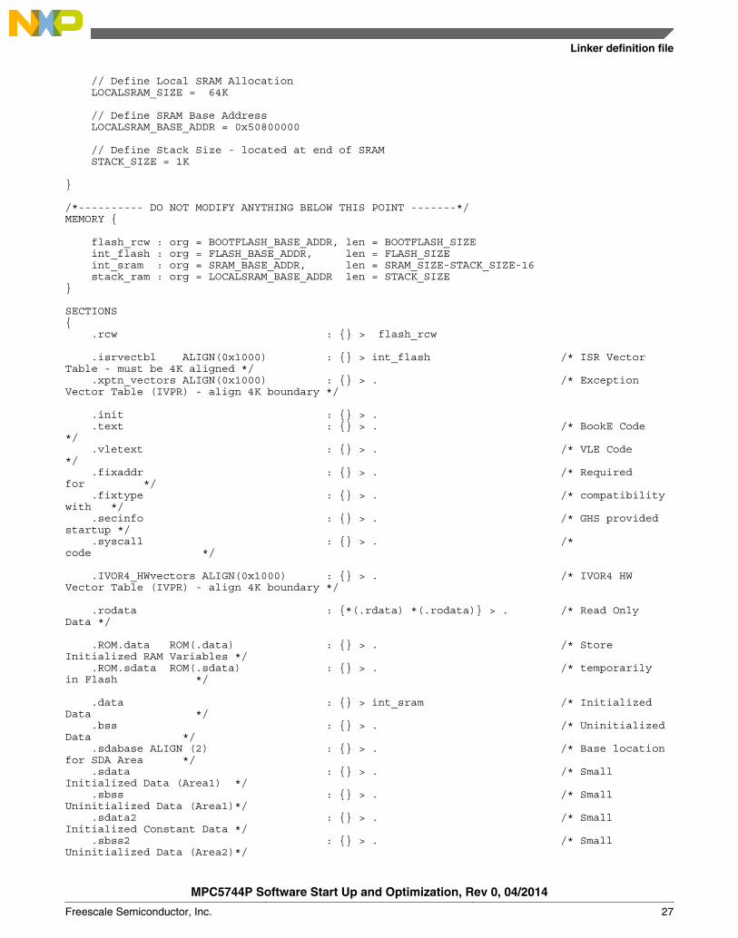
// Define Local SRAM Allocation LOCALSRAM_SIZE = 64K
// Define SRAM Base Address LOCALSRAM_BASE_ADDR = 0x50800000
// Define Stack Size - located at end of SRAM STACK_SIZE = 1K }
/*---------- DO NOT MODIFY ANYTHING BELOW THIS POINT -------*/MEMORY {
flash_rcw : org = BOOTFLASH_BASE_ADDR, len = BOOTFLASH_SIZE int_flash : org = FLASH_BASE_ADDR, len = FLASH_SIZE int_sram : org = SRAM_BASE_ADDR, len = SRAM_SIZE-STACK_SIZE-16 stack_ram : org = LOCALSRAM_BASE_ADDR len = STACK_SIZE}
SECTIONS{ .rcw : {} > flash_rcw .isrvectbl ALIGN(0x1000) : {} > int_flash /* ISR Vector Table - must be 4K aligned */ .xptn_vectors ALIGN(0x1000) : {} > . /* Exception Vector Table (IVPR) - align 4K boundary */ .init : {} > . .text : {} > . /* BookE Code */ .vletext : {} > . /* VLE Code */ .fixaddr : {} > . /* Required for */ .fixtype : {} > . /* compatibility with */ .secinfo : {} > . /* GHS provided startup */ .syscall : {} > . /* code */
.IVOR4_HWvectors ALIGN(0x1000) : {} > . /* IVOR4 HW Vector Table (IVPR) - align 4K boundary */ .rodata : {*(.rdata) *(.rodata)} > . /* Read Only Data */ .ROM.data ROM(.data) : {} > . /* Store Initialized RAM Variables */ .ROM.sdata ROM(.sdata) : {} > . /* temporarily in Flash */
.data : {} > int_sram /* Initialized Data */ .bss : {} > . /* Uninitialized Data */ .sdabase ALIGN (2) : {} > . /* Base location for SDA Area */ .sdata : {} > . /* Small Initialized Data (Area1) */ .sbss : {} > . /* Small Uninitialized Data (Area1)*/ .sdata2 : {} > . /* Small Initialized Constant Data */ .sbss2 : {} > . /* Small Uninitialized Data (Area2)*/
Linker definition file
MPC5744P Software Start Up and Optimization, Rev 0, 04/2014
Freescale Semiconductor, Inc. 27
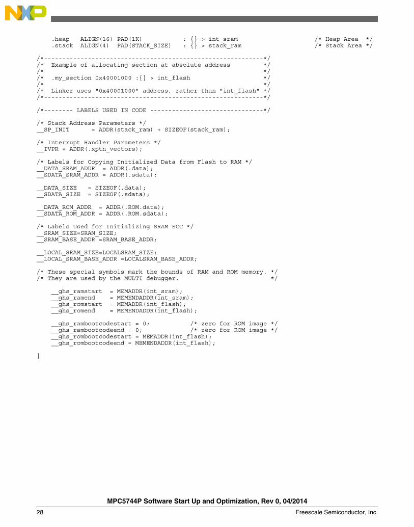
.heap ALIGN(16) PAD(1K) : {} > int_sram /* Heap Area */ .stack ALIGN(4) PAD(STACK_SIZE) : {} > stack_ram /* Stack Area */
/*------------------------------------------------------------*//* Example of allocating section at absolute address *//* *//* .my_section 0x40001000 :{} > int_flash *//* *//* Linker uses "0x40001000" address, rather than "int_flash" *//*------------------------------------------------------------*/
/*-------- LABELS USED IN CODE -------------------------------*/ /* Stack Address Parameters */__SP_INIT = ADDR(stack_ram) + SIZEOF(stack_ram);
/* Interrupt Handler Parameters */__IVPR = ADDR(.xptn_vectors);
/* Labels for Copying Initialized Data from Flash to RAM */__DATA_SRAM_ADDR = ADDR(.data);__SDATA_SRAM_ADDR = ADDR(.sdata);
__DATA_SIZE = SIZEOF(.data);__SDATA_SIZE = SIZEOF(.sdata);
__DATA_ROM_ADDR = ADDR(.ROM.data);__SDATA_ROM_ADDR = ADDR(.ROM.sdata);
/* Labels Used for Initializing SRAM ECC */ __SRAM_SIZE=SRAM_SIZE;__SRAM_BASE_ADDR =SRAM_BASE_ADDR;
__LOCAL_SRAM_SIZE=LOCALSRAM_SIZE;__LOCAL_SRAM_BASE_ADDR =LOCALSRAM_BASE_ADDR;
/* These special symbols mark the bounds of RAM and ROM memory. *//* They are used by the MULTI debugger. */
__ghs_ramstart = MEMADDR(int_sram); __ghs_ramend = MEMENDADDR(int_sram); __ghs_romstart = MEMADDR(int_flash); __ghs_romend = MEMENDADDR(int_flash);
__ghs_rambootcodestart = 0; /* zero for ROM image */ __ghs_rambootcodeend = 0; /* zero for ROM image */ __ghs_rombootcodestart = MEMADDR(int_flash); __ghs_rombootcodeend = MEMENDADDR(int_flash);
}
MPC5744P Software Start Up and Optimization, Rev 0, 04/2014
28 Freescale Semiconductor, Inc.

How to Reach Us:
Home Page:freescale.com
Web Support:freescale.com/support
Information in this document is provided solely to enable system andsoftware implementers to use Freescale products. There are no expressor implied copyright licenses granted hereunder to design or fabricateany integrated circuits based on the information in this document.Freescale reserves the right to make changes without further notice toany products herein.
Freescale makes no warranty, representation, or guarantee regardingthe suitability of its products for any particular purpose, nor doesFreescale assume any liability arising out of the application or use ofany product or circuit, and specifically disclaims any and all liability,including without limitation consequential or incidental damages.“Typical” parameters that may be provided in Freescale data sheetsand/or specifications can and do vary in different applications, andactual performance may vary over time. All operating parameters,including “typicals,” must be validated for each customer application bycustomer's technical experts. Freescale does not convey any licenseunder its patent rights nor the rights of others. Freescale sells productspursuant to standard terms and conditions of sale, which can be foundat the following address: freescale.com/SalesTermsandConditions.
Freescale, Freescale logo, SafeAssure, SafeAssure logo, and Qorivvaare trademarks of Freescale Semiconductor, Inc., Reg. U.S. Pat. & Tm.Off. MagniV is trademark of Freescale Semiconductor, Inc. The PowerArchitecture and Power.org word marks and the Power and Power.orglogos and related marks are trademarks and service marks licensed byPower.org. All other product or service names are the property of theirrespective owners.
© 2014 Freescale Semiconductor, Inc.
Document Number AN4939Revision 0, 04/2014