Embed Size (px)
Citation preview

5
5
4
4
3
3
2
2
1
1
D D
C C
B B
A A
X5
Freescale AISG Applications, East Kilbride
X6
X2
X3
X4
Audio - SAI Audio. AVB and TWRPI headers
Revision Information
0.1
Designer
Alasdair Robertson
CommentsRev Date
Power - Switching voltage regulators
Reset and External Clock Input
Sheet 8
Sheet 9
Sheet 10
Sheet 11
Sheet 12
Sheet 13
Sheet 14
Sheet 15
Sheet 16
These schematics are provided for reference purposes only. As such,Freescale does not make any warranty, implied or otherwise, as to thesuitability of circuit design or component selection (type or value) used inthese schematics for hardware design using the Freescale Calypso familyof Microprocessors. Customers using any part of these schematics as abasis for hardware design, do so at their own risk and Freescale does notassume any liability for such a hardware design.
Sheet 2
Sheet 3
Sheet 4
Sheet 5
Sheet 6
Sheet 7Comms - CAN and LIN
Comms - Ethernet
Comms - USB Interfaces
Memory - SD Card Slot
AV - MOST Interface
User notes are given throughtout the schematics.
Specific PCB LAYOUT notes are detailed in ITALICS
Caution:
19 Feb 2012
Comms - RS232 (USB FTDI interface)
Comms - FlexRAY
User - Switches, LED's and Potentiometer
User - GPIO Pin Matrix
Table Of Contents:
Notes:
MPC574xx Customer Evaluation Board (X-MPC574XG-MB)
- All components and board processes are to be ROHS compliant- All small capacitors are 0402 unless otherwise st ated- All resistors are 0603 5% 0.1w unless otherwise s tated. All zero ohm links are 0603- All connectors and headers are denoted Px and are 2.54mm pitch unless otherwise stated- All jumpers are denoted Jx. Jumpers are 2mm pitch- Jumper default positions are shown in the schemat ics. For 3 way jumpers, default is always posn 1-2. 2 Pin jumpers generally have the "source" on pin 1.- All switches are denoted SWx- All test points (SMT wire loop style) are denoted TPx- Test point Vias (just through hole pads) are deno ted TPVx
X1Power - Main input and Linear voltage regulators
Daughter Card Connectors (Sockets)
JTAG and Nexus Connectors
Start of capture, Working version01 Feb 2012
1st release for internal review (Complete Board)
28 Feb 2012
Alasdair Robertson
Alasdair Robertson 2nd release for internal review (split into main board and DC)
Signals (ports) have not been routed via busses as this makes it harder to determine where each signal goes.
Alasdair Robertson
Version sent to Pre Layout, incorporating fixes from review
Final review (including new USB transceiver)11 Mar 2013
Alasdair Robertson13 Mar 2013
14 Mar 2013 Alasdair Robertson Component consolodation, Few minor changes. Sent to Layout
3 Different test points used in design:
TPVx - Through Hole Pad small
TPHx - Through Hile Pad Large (for standard 0.1" he ader).Also used on IO Matrix (IOMx)
TPX - Surface Mount Wire Loop
29 Mar 2013 Alasdair Robertson Changes made during layout to Daughtercard Connectors
A Post Layout (Back Annotated). Matches PCB RevAAlasdair Robertson
02 Apr 2013 Alasdair Robertson LAY RefDes Resequence and SCH BackAnnotateX7
17 Apr 2013
AX1 24 Jun 2013 Alasdair Robertson Fixes and changes to RevA Prototype design
AX2 10 July 2013 Alasdair Robertson Added CAN Term (DNP)
AX3 12 July 2013 Alasdair Robertson Corrected ground on ADC Pot
B 12 July 2013 Alasdair Robertson Production Release
BX1 20 Aug 2013 Alasdair Robertson Change to Ethernet 50MHz clock control
C 20 Aug 2013 Alasdair Robertson Production Release
CX1 18 Dec 2013 Alasdair Robertson CAN transceivers -> MC33901, ENET clock in RMII mode
CX2 05 May 2014 Alasdair Robertson Added comment about LM1117 VREG output
CX3 25 June 2014 Alasdair Robertson PH3..5 now GPIO matrix (was SAI), PM4, PD13, PM3 to SAI
CX4 26 June 2014 Alasdair Robertson Minor changes made during layout (no component changes)
CX5 26 June 2014 Alasdair Robertson Part Manager Tidy up
CX6 18 Aug 2014 Alasdair Robertson Added additional connector with DSPI Signals for AVB
CX7 03 Sept 2014 Alasdair Robertson Added additional TWRPI header (Sheet 12)
D 24 Sept 2014 Alasdair Robertson Released to Production (RevD PCB)
Drawing Title:
Size Document Number Rev
Date: Sheet of
Page Title:
Designer:
Drawn by:
Approved:
Automotive Microcontroller ApplicationsEast Kilbride, Scotland
This document contains information proprietary to Freescale and shall not be used for engineering design,
procurement or manufacture in whole or in part without the express written permission of Freescale
SCH-27897 PDF: SPF-27897 D
MPC574XG-MB
B
Tuesday, September 30, 2014
Index and Title Page
A. Robertson
A. Robertson
A. Robertson
1 16
Freescale General Business Use

5
5
4
4
3
3
2
2
1
1
D D
C C
B B
A A
Rfb1
Rfb2
Main EVBPower In
Vout = 1.25(1 + (R2/R1)) = 5.0V
(060350V)
GND Test Points, Top Side
Rfb1
Rfb2
Vout = 1.25(1 + (R2/R1)) = 3.295V
3.3V Linear Regulator (800mA Max **)
(35V TANT)(35VTANT)
(0402 50V)
Could also use 2x82 Ohm resistors for RFB2 but not in agile...
1% resitors1% resitors
Rfb1
Rfb2
Vout = 1.25(1 + (R2/R1)) = 1.25V
1% resitors
1.25V Linear Regulator (800mA Max **)
(35V TANT)(35VTANT)
Power Input and Linear Voltage Regulators
Input 12V DC nominal (range 10v - 14v)See note on schematic sheet 3 regarding 3.3V regula tor when running at < 11V)
1.25V for External core supply. Simpler to use line ar rather than switcher so can safelypower from 5V switcher (slight ripple not an issue) for reduced heat dissipation
(c200 radpol 50V)
2.1mm BarrelConnector
(2 Screw Connector)
(Power Switch)
Power Supply Input and Filter Test and reference points
GND Test Points for underside of board
5.0V Linear Regulator (800mA Max **)
(35V TANT)(35VTANT)
(CC7343-4325V)
(10v-14v)
(3A)
(3A)
1K Loadresistor toensure properregulation if1.25V MCUjumper removed
The LM1117 linear regulators provide a maximum outp utcurrent of 800mA in ideal conditions. The currentrequirement for each regulator is in the region of 10'sof mA (significantly under the maximum rating) sothese regulators will run cool on the EVB.
** Notes on Linear Regulator LM1117
VFused12V-IN VSwitched
3V3_LRP12V
GND
1V25_LR
GND
P12V
5V0_SR
GND
P12V
GND
GND
GND
5V0_LRP12V
GND
GND
P12V
Drawing Title:
Size Document Number Rev
Date: Sheet of
Page Title:
Automotive MicrocontrollerApplications
East Kilbride, Scotland
SCH-27897 PDF: SPF-27897 D
MPC574XG-MB
B
Tuesday, September 30, 2014
Power Input and Linear Voltage Regulators
2 16
Freescale General Business Use
Drawing Title:
Size Document Number Rev
Date: Sheet of
Page Title:
Automotive MicrocontrollerApplications
East Kilbride, Scotland
SCH-27897 PDF: SPF-27897 D
MPC574XG-MB
B
Tuesday, September 30, 2014
Power Input and Linear Voltage Regulators
2 16
Freescale General Business Use
Drawing Title:
Size Document Number Rev
Date: Sheet of
Page Title:
Automotive MicrocontrollerApplications
East Kilbride, Scotland
SCH-27897 PDF: SPF-27897 D
MPC574XG-MB
B
Tuesday, September 30, 2014
Power Input and Linear Voltage Regulators
2 16
Freescale General Business Use
DS6
LED GREEN
AC
R3051K
GND13
1
GND4
1
C2680.1UF
TP17
1
L527uH
1 2F1
Fuse Holder
1 2
GND10
1
R77 0
R72 100
DNP
GND17
1
GND7
1
GND1
1
+ C27
10UF R73 100
U16
LM1117MPX-ADJ
ADJ1
VOUT2IN
3TAB_VOUT
4
R273270
GND5
1
P23
A1
B2
+ C26
10UF
U15
LM1117MPX-ADJ
ADJ1
VOUT2IN
3TAB_VOUT
4
GND8
1
+ C30
10UF
DS5
LED GREEN
AC
R76 0
GND12
1
+ C321000UF
GND2
1
DS4
LED GREEN
A C
GND15
1
+ C29
10UF
C2691000pF
R74 100
P211
32
R271 5.6
GND3
1
R284 0
+C3368UF
R75 0
DNP
SW51 34 2
5
R272 0R70 300
GND11
1
+ C28
10UF
GND9
1
TP16
1
GND14
1
TP15
1
D202B340A
AC
R274560
U14
LM1117MPX-ADJ
ADJ1
VOUT2IN
3TAB_VOUT
4
GND6
1
J23
1
2
3
GND16
1
R285 0
GND18
1
Q1BSH103
1
23
R71 158
+ C31
10UF
R283 1.8K

5
5
4
4
3
3
2
2
1
1
D D
C C
B B
A A
Design requiresB220A-13-Fdiode. Use3Aversion toreduce no ofcomponents
(12v input, 2.0A Output, 89% Efficient, 11.24w)
Switching Voltage Regulators and Supply Jumpers
5.0v Switching Regulator
(121025V)
(060350V)
(0603 50V)
(All Resistors 1% 0603_CC)
Rfb1
Rfb2
Vout = 1.21(1 + Rfb2/Rfb1) = 4.98V
APXE100ARA151MF80G
(121025V)
APXE100ARA151MF80G
(060350V)
3.3v Switching Regulator
(12v input, 2A Output, 83% Efficient)
(0603 50V)
(All Resistors 1% 0603_CC)
Rfb1
Rfb2
Vout = 1.21(1 + Rfb2/Rfb1) = 3.3V
Using Adjustable version of LM2676 rather than fixe d 3.3V /5V regulators to reduce number of components in BOM .
Where possible, components have been shared accross theregulator designs to further reduce component count .
The 3.3v regulator design is optimised for an inpu t voltage of 12V. Ifthe input voltage drops below approx 11V, the 3.3v output voltageripple may increase. This can be reduced by increas ing the bulk storagecapacitor if required.
Caution
Global MCU DaughtercardSupply Jumpers and DC power
Peripheral Power Control
These jumpers control the voltage of theperipherals connected to MCU pads in theVDD_HV_A / HV_B domains and are requiredso the respective jumpers at the MCU canbe used for MCU current measurement.
The settings on these jumpers mustmirror the setting of the respectiveMCU VDD_HV_A / HB_V jumpers
To DaughtercardConnectors
MCU_3V3_S
MCU_5V0_S
MCU_3V3_L
MCU_5V0_L
MCU_1V25_L
DC_5V0_S
DC_3V3_S
DC_5V0_L
DC_3V3_L
DC_1V25_L
DC_P12V
P12V
GND
5V0_SR
GND
GND
3V3_SR
P12V
GND
3V3_SR
5V0_SR
3V3_LR
5V0_LR
1V25_LR
5V0_SR
3V3_SR
PER_HVA PER_HVB
P12V
DC_5V0_S 4
DC_3V3_S 4
DC_5V0_L 4
DC_3V3_L 4
DC_1V25_L 4
DC_P12V 4
MCU_1V25_L 4
MCU_5V0_S 4
MCU_5V0_L 4
MCU_3V3_S 4
MCU_3V3_L 4
Drawing Title:
Size Document Number Rev
Date: Sheet of
Page Title:
Automotive MicrocontrollerApplications
East Kilbride, Scotland
SCH-27897 PDF: SPF-27897 D
MPC574XG-MB
B
Tuesday, September 30, 2014
Switching Voltage Regulators
3 16
Freescale General Business Use
Drawing Title:
Size Document Number Rev
Date: Sheet of
Page Title:
Automotive MicrocontrollerApplications
East Kilbride, Scotland
SCH-27897 PDF: SPF-27897 D
MPC574XG-MB
B
Tuesday, September 30, 2014
Switching Voltage Regulators
3 16
Freescale General Business Use
Drawing Title:
Size Document Number Rev
Date: Sheet of
Page Title:
Automotive MicrocontrollerApplications
East Kilbride, Scotland
SCH-27897 PDF: SPF-27897 D
MPC574XG-MB
B
Tuesday, September 30, 2014
Switching Voltage Regulators
3 16
Freescale General Business Use
D5B340A
AC
C266
0.1UF
R267 0DNP
TP19
1
J181 2
TP20
1
C267
0.1UF
R297 261.0
C265 10nF
R291 0
R266 0DNP
C264 10nF
+ C36
150uF
D6B340A
AC
R298 1.65K
J28
DNP
12
J211 2
R294 0
J25
1
2
3
C34
10uF
R300
560
J201 2
U17 LM2676S-ADJ
INPUT2
SW_OUT1
C_BOOST3
GN
D4
TA
B8
FEEDBACK6
ON/OFF7
NC5 R263 0
DNP
DS9
LED GREEN
AC
J191 2
DS10
LED GREEN
AC
R293 1.47K
R265 0DNP
C35
10uF
R292 1.0K
U18 LM2676S-ADJ
INPUT2
SW_OUT1
C_BOOST3
GN
D4
TA
B8
FEEDBACK6
ON/OFF7
NC5
R264 0DNP
R268 0DNP
J241
2
3
L7 27uH1 2
R296 1.47K
J27DNP
12
R295 1.0K
+ C37
150uF
L6 27uH1 2
R299270
J221 2

5
5
4
4
3
3
2
2
1
1
D D
C C
B B
A A
Socket
Not routed through the connectors:- Crystal signals- Specific MCU power pins (Power supplies are howev er taken to daughtercard)
(GND)
(GND)
(GND)
(GND)
(GND)
(GND)
(GND)
(GND)
(GND)
(GND)
(GND)
(GND)
(GND)
(GND)
(GND)
(GND)
(GND)(GND)(GND)
(GND)
(GND)
(GND)
(GND)
(GND)
(GND)
(GND)
(GND)
(GND)(GND)
(GND)
(GND)
(GND)
(GND)
(GND)
(GND)
(GND)
(GND)
(GND)(GND)
(GND)
(GND)
(GND)
(GND)
(GND)
(GND)
(GND)(GND)
(GND)
(GND)
(GND)
(GND)(GND)
(GND)
(GND)
(GND)
(GND)
(GND)
(GND)(GND)
(GND)
(GND)
(GND)
(GND)
(GND)
(GND)
(GND)
(GND)
(GND)
(GND)
Daughter Card Connectors (Sockets)
Socket
Notes:
- there was no neat way to fit these connectors ont o a B sized sheet so unfortunately the sheet size h as beenincreased to C so will need to be printed on larger paper.
- The MCU Clock circuitry (apart from external cloc k) is local to the daughtercard so not pinned out o n theconnectors- Power is supplied to the daughtercard via MCU spe cific jumpered supplies (left connector) or direct suppliesfrom the regulators (right connector)
(GND) (GND)
(GND)
(GND)
(GND)
(GND)
(GND)
(GND)
(GND)
(GND) (GND)
(GND)(GND)
(GND)
(GND)(GND)
(GND)(GND)
(GND)
(GND)(GND)
(GND) (GND)
(GND)
(GND)
(GND)
(GND) (GND)PM11 PC1PH10 PE3PH4 PH5
PL4
PE15
PL9
PL3
PH12
PG11
PG10
PL8
PORSTx
PH11
PE14
PG15
PC4
PQ1
PQ2
PQ6
PP13PP12
PE2
PA6
PA5
PQ4
PQ5PQ7 PI4PP15 PP14
PL12 PL2
PL13PL6PM0
PM10
PL7
PM8PH3
PM6
PI11PI12PD12PD9PD13
PI15PD10PB7
PB3PH8
PH7
PP8
PH6
PP3PE7PK9
PC12PK11
PP4PC8 PK14PK13 PK12
PC9PP2 PL0PK15PC15 PP1PP7
PC14PP6 PJ4
PO12PO7PO10PO4 PH14PO9 PO13
PO1PG5PH13PO14
PO0 PG4PI7 PH15PP0 PO15
PE10PE1 PE0PI6 PO6PO5PE11 PG2PG3 PA2
PE9PE8 PA1
MCU-RSTxPG9 PN15PA0 PO3
PG7 PG6PG8 PC11PC10 PO2
PB0
PB10PN0
PN6PN3PA15PN10
PA4PJ13
PN9PJ9
PB1 PK1PK2 PF12
PK3PK5PF11
PF9PA14PN13
PN11PJ11PJ10PK0
PL10
PE5
PG14
PM12
PQ0PI5
PC5
PQ3
PE4PC3
PC2
PA8
PH2-RPG0-RPF14
PA9PA10
PA7
PG1PF15PE13
PA11PE12
PL11 PL5
PH1-RPH0-RPA3
PG12-RPG13-R
PI13
PM4PL1
PM5
PM3
PM14PM13
PB12
PF5PI9PD8
PJ3PJ2PB4
PM15PF2
PD7PJ5PJ0
PD5PB5
PJ1PD1PB11
PI10PD0PB6
PN1PF6PD4
PI14PJ7PD11PJ6PD6PD2
PJ8PD3
MLB_DATMLB_CPMLB_CN
MLB_CLKMLB_SIG
MLB_SNMLB_SP
MCU_5V0_S
MCU_1V25_L
MCU_3V3_S
MCU_3V3_LMCU_5V0_L
PO11PO8
PA12
PF0PF1PN2
PN5
PA13PN4
PJ14PN7PF10PN8
PJ15
PC7PN12PJ12
PF8
PK7PC6
PF13PK4PK6
PN14PK8
DC_3V3_S
DC_5V0_LDC_3V3_L
DC_5V0_SDC_5V0_SDC_5V0_S
DC_P12VDC_1V25_L
PF3PF7PF4
PL15
PM2PM1
PL14
PM7PM9
MLB_DNMLB_DP
PE6PI3PP10PP5PI1PI2PP9PC13PI0PK10
PB2
PP11
EXT-CLK
PC0
PH9
GND GNDGND GND
PH7 13
PH6 13
PB3 7
PP8 16PH8 14
PP3 16
PE7 14
PK9 16
PC12 11
PK11 16
PP4 16
PK14 16
PK12 16
PC9 8
PL0 16
PP1 16
PC14 11
PJ4 16
PH14 16
PO13 16
PO1 12,16
PH13 16
PG4 12,15,16
PH15 16
PO15 16
PE10 12
PE0 13
PO6 16
PG2 12,15,16
PA2 15,16
PE9 12
PA1 15,16
MCU-RSTx 5,6
PN15 16
PO3 16
PG6 16
PC11 7
PO2 16
PB0 7
PK1 12,16
PF12 16
PK3 12,16
PK5 16
PF11 15,16
PC1 6
PE3 11
PH5 16
PQ3 9
PC3 9
PE4 11
PL10 6
PE15 9
PORSTx 5
PE2 11
PL4 6
PG11 9
PQ1 9
PG10 9
PQ2 9
PL8 6
PQ6 9
PP13 9
PP12 9
PI4 9
PP14 9
PL2 6
PL5 6
PL13 6
PM0 6
PA10 10
PA9 10
PA8 10
PF14 10
PG0-R 10
PH2-R 10
PG12-R 10
PG13-R 10
PM10 6
PM4 12,16
PL1 16
PM5 16
PI13 13,16
PB12 16
PD9 16
PI12 13,16
PB7 16
PI15 12
MLB_CN 13
MLB_CP 13
PI14 12
PJ7 16
PD11 16
PJ6 16
PD6 12,16
PD2 15,16
PD3 15,16
PJ8 16
PB6 16
PD0 15,16
PI10 16
PD4 12,16
PF6 12
PN1 16
PC88
PK1316
PP216
PK1516
PC1511
PP716
PP616
PO1216
PO716
PO1016
PO416
PO916
PG512,15,16
PO1416
PO012,16
PI79
PP016
PE113
PI69
PO516
PE1112
PG312,15,16
PE812
PG913
PA014
PG716
PG816
PC107
PB17
PK212,16
PF915,16
PA1412,16
PN1316
PN1116
PJ1116
PJ1016
PK012,16
PJ916
PN916
PJ1316
PA416
PN1016
PA1512,16
PN316
PN616
PN016
PB1012
PM1116
PH106
PH416
PE511
PM1216
PI59
PQ09
PC511
PG149
PH129
PC411
PL96
PC29
PA613
PL36
PH119
PA512
PE149
PQ49
PG159
PQ59
PQ79
PP159
PL126
PL116
PL66
PL76
PE1210
PA1110
PA710
PE1310
PF1510
PG110
PH1-R10
PH0-R10
PA310
PM86
PH316
PM312,16
PM616
PM1316
PM1416
PD1312,13,16
PD1216
PI1110
PD1016
MLB_DAT13
MLB_SIG13
MLB_CLK13
MLB_SN13
MLB_SP13
PD712,16
PJ516
PJ012
PD512,16
PB516
PB1116
PD115,16
PJ112
PD812,16
PI916
PF512
PB415
PJ212
PJ312
PF212
PM1516
MCU_5V0_S3
MCU_1V25_L3
PO11 16
PO8 16
PN5 16
PA12 12,16
PN2 16
PF1 12
PF0 12
PN4 16
PA13 12,16
PN8 16
PF10 16
PN7 16
PJ14 16
PJ15 16
PC7 7
PN12 16
PJ12 16
PF8 16
PK7 16
PC6 7
PF1316
PK412,16
PK616
PK816
PN1416
DC_5V0_S3
DC_P12V3
DC_1V25_L3
PF4 12
PF7 12
PF3 12
PL156
PM16
PM26
PL14 6
PM9 6
PM7 6
MLB_DN 13
MLB_DP 13
PE614
PI314
PP1016
PP516
PI114
PI214
PP916
PC1311
PI014
PK1016
PB27
PP1116
EXT-CLK5
PC0 6
PH9 6
MCU_3V3_S 3
MCU_3V3_L 3MCU_5V0_L 3
DC_3V3_S 3
DC_3V3_L 3DC_5V0_L 3
Drawing Title:
Size Document Number Rev
Date: Sheet of
Page Title:
Automotive MicrocontrollerApplications
East Kilbride, Scotland
SCH-27897 PDF: SPF-27897 D
MPC574XG-MB
C
Tuesday, September 30, 2014
Daughter Card Connectors (Sockets)
4 16
Freescale General Business Use
Drawing Title:
Size Document Number Rev
Date: Sheet of
Page Title:
Automotive MicrocontrollerApplications
East Kilbride, Scotland
SCH-27897 PDF: SPF-27897 D
MPC574XG-MB
C
Tuesday, September 30, 2014
Daughter Card Connectors (Sockets)
4 16
Freescale General Business Use
Drawing Title:
Size Document Number Rev
Date: Sheet of
Page Title:
Automotive MicrocontrollerApplications
East Kilbride, Scotland
SCH-27897 PDF: SPF-27897 D
MPC574XG-MB
C
Tuesday, September 30, 2014
Daughter Card Connectors (Sockets)
4 16
Freescale General Business Use
P12
CON SKT 180
1SH1 SH2
SH5 SH6
23 45 67 89 10
11 1213 1415 1617 1819 2021 2223 2425 2627 2829 3031 3233 3435 3637 3839 4041 4243 4445 4647 4849 5051 5253 5455 5657 5859 60
SH3 SH4
61 6263 6465 6667 6869 7071 7273 7475 7677 7879 8081 8283 8485 8687 8889 9091 9293 9495 9697 9899 100
101 102103 104105 106107 108109 110111 112113 114115 116117 118119 120SH7 SH8
SH9 SH10121 122123 124125 126127 128129 130131 132133 134135 136137 138139 140141 142143 144145 146147 148149 150151 152153 154155 156157 158159 160161 162163 164165 166167 168169 170171 172173 174175 176177 178179 180
SH11 SH12
P13
CON SKT 180
1SH1 SH2
SH5 SH6
23 45 67 89 10
11 1213 1415 1617 1819 2021 2223 2425 2627 2829 3031 3233 3435 3637 3839 4041 4243 4445 4647 4849 5051 5253 5455 5657 5859 60
SH3 SH4
61 6263 6465 6667 6869 7071 7273 7475 7677 7879 8081 8283 8485 8687 8889 9091 9293 9495 9697 9899 100
101 102103 104105 106107 108109 110111 112113 114115 116117 118119 120SH7 SH8
SH9 SH10121 122123 124125 126127 128129 130131 132133 134135 136137 138139 140141 142143 144145 146147 148149 150151 152153 154155 156157 158159 160161 162163 164165 166167 168169 170171 172173 174175 176177 178179 180
SH11 SH12

5
5
4
4
3
3
2
2
1
1
D D
C C
B B
A A
TARGETRESETLED
Reset Switch(1.65 to 5.5v operation)
(MCU RESET)
Tri-State BufferedRESET signal toreset the MCU
Reset and External Clock In
Buffered RESET-out
Note:
The Reset pad on Calypso is in the VDD_HV_A domain which can be run from either 3.3V or 5V(selected by the VDD_HV_A and PER_HVA jumpers)
To maintian brightness on the LED's irrespective of the voltage setting, the LED's arepowered from constant 3.3V, grounded via the reset line.
Bi Directional resetline to/from MCU
Active reset drive (high / low)for any periperhals that need tobe reset when MCU is in reset
Reset fromDebugger
Reset Input / OutputPORST
Connect an external LVI to padwhen supplying external 1.25V sothat PORST is asserted untilexterbal 1.25V supply is atthreshold and stable
(2.5 to 5v operation)
SMA styleConnector
External Clock In (SMA)
(060350V)(0603
50V)
(060350V)
Reset is in theVDD_HVA domain.
MCU-RSTxJTAG-RSTx
RST-SWITCHx
RST-OUTx
RST-INxSYSTEM-RSTx
PORSTx
EXT-CLK
GND
GND
GND
3V3_SR
GND
GND
PER_HVA
3V3_SR
PER_HVA
GND
JTAG-RSTx6
MCU-RSTx 4,6
RST-OUTx 10,12
PORSTx 4
EXT-CLK 4
Drawing Title:
Size Document Number Rev
Date: Sheet of
Page Title:
Automotive MicrocontrollerApplications
East Kilbride, Scotland
SCH-27897 PDF: SPF-27897 D
MPC574XG-MB
B
Tuesday, September 30, 2014
Reset Circuitry & External Clock In
5 16
Freescale General Business Use
Drawing Title:
Size Document Number Rev
Date: Sheet of
Page Title:
Automotive MicrocontrollerApplications
East Kilbride, Scotland
SCH-27897 PDF: SPF-27897 D
MPC574XG-MB
B
Tuesday, September 30, 2014
Reset Circuitry & External Clock In
5 16
Freescale General Business Use
Drawing Title:
Size Document Number Rev
Date: Sheet of
Page Title:
Automotive MicrocontrollerApplications
East Kilbride, Scotland
SCH-27897 PDF: SPF-27897 D
MPC574XG-MB
B
Tuesday, September 30, 2014
Reset Circuitry & External Clock In
5 16
Freescale General Business Use
R2410.0K
R214 270
J9
1 2
R3110.0K
SW1 B3WN-6002
1 2
C3
0.1UF
VCC
GND
U4A
SN74LVC2G08DCT
1
27
84
TPV5
R217270
P7
CON 1 SMA
1
24 35
R410.0K
U4B
SN74LVC2G08DCT
5
63
U3
ADM6315-26D2ARTZR7
GND
1
RESET2
MR3
VCC
4
C2200.1UF
R216100
C2240.1UF
R1610.0K
TPH1
1
DS1YELLOW LED
AC
D1
LED RED
A C
5
5
4
4
3
3
2
2
1
1
D D
C C
B B
A A
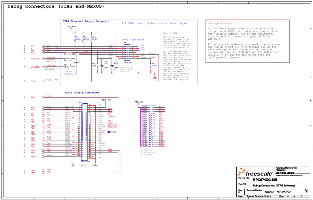
Debug Connectors (JTAG and NEXUS)
JTAG Standard 14-pin Connector
(RDY)
Place One CAPnext to eachconnector
ONCE Connector
(N/C)(TMS)
(JCOMP)
(GND)(GND)(GND)
(GND)
(TDI)(TDO)(TCLK)(EVTI)(RESET)(VREF)
TDITDOTCLK
(All JTAG reset pullups are on Reset Page)
(MSEO_0)(MSEO_1)
(MDO4)
(GND)
(GND)
(GND)
(GND)
(TMS)(TDI)(TDO)
(GND)
(GND)
(GND)
(GND)
(JCOMP)(RDY)(EVTI)(EVTO)
(GND)
(GND)
(MDO0)
(RST OUT)(RESET)
(GND)
(GND)
(GND)
(GND)
(MDO1)
(MDO2)(MDO3)
(MCKO)
(N/C)
(MDO5)(MDO6)
(MDO7)(MDO8)
(MDO9)(MDO10)
(MDO14)
(ARBREQ)(ARBGRT)
(MDO15)
(MDO13)(MDO12)(MDO11)
(GND)
(VREF)(TCK)
(CLKOUT)(TD/WT)
(DAI1)(DAI2)
Nexus
(bufferedreset TO MCU)
(bidirectionalMCU reset)
Note on EVTI:
EVTI is an optionalsignal. Although it issupported on the JTAGconnector, tools vendorsdo not normally use EVTIon non trace hardware.
EVTI is powered from VDD_HV_B whereas therest of the JTAG signalsare from VDD_HV_A. Inorder to use EVTI on theJTAG, connector,VDD_HV_A and HV_B shouldbe set to the samevoltage. Rather thanimpose this limitationfor all customers, azero ohm link has beenadded to allow EVTI tobe enabled on the JTAGconnector if required.
OptionalConfig
EVTI
TMS
NEXUS 50-pin Connector
NeusSpecificPullups all10K 0603
All of the signals used for JTAG (with theexception of EVTI, see note) are powered fromthe VDD_HV_A domain. All of the additionalsignals used for Nexus are powered fromVDD_HV_B.
If you are using Nexus, you need to ensure thatthe VDD_HV_A and VDD_HV_B domains are at thesame voltage as well as ensuring that theperipheral supplies PER_HVA and PER_HVB matchVDD_HV_A / B. See the MCU power page forconfiguration jumpers.
Voltage Domains:
EVTI
JCOMP
PH10
PC0PC1
PH10
PH9
DBUG-RSTx
PL9PL11
PL2PL3
PL4PL5
PL10PL6
PL7PL13
PL14PL15
PM0PM1
PM2PM7
PM10
PH9PH10PC0PC1JCOMP
PL8PL12DBUG-RSTx
PM8PM9
MCU-RSTx
JTAG-RSTx
MCU-RSTx
PL8
PM9PM8
PL12
PL9PL11PL2PL3PL4PL5PL10PL6PL7PL13PL14PL15PM0PM1PM2
PL12
PM7PM10PM9PM8
GND
GND GND
PER_HVA
PER_HVBPER_HVB
PH94
PC04
PC14
JTAG-RSTx5
MCU-RSTx4,5
PL84
PH104
PL124
PL74
PL94
PL114
PL24
PL34
PL44
PL54
PL104
PL64
PL134
PL144
PL154
PM04
PM14
PM24
PM74
PM104
PM94
PM84
Drawing Title:
Size Document Number Rev
Date: Sheet of
Page Title:
Automotive MicrocontrollerApplications
East Kilbride, Scotland
SCH-27897 PDF: SPF-27897 D
MPC574XG-MB
B
Tuesday, September 30, 2014
Debug Connectors (JTAG & Nexus)
6 16
Freescale General Business Use
Drawing Title:
Size Document Number Rev
Date: Sheet of
Page Title:
Automotive MicrocontrollerApplications
East Kilbride, Scotland
SCH-27897 PDF: SPF-27897 D
MPC574XG-MB
B
Tuesday, September 30, 2014
Debug Connectors (JTAG & Nexus)
6 16
Freescale General Business Use
Drawing Title:
Size Document Number Rev
Date: Sheet of
Page Title:
Automotive MicrocontrollerApplications
East Kilbride, Scotland
SCH-27897 PDF: SPF-27897 D
MPC574XG-MB
B
Tuesday, September 30, 2014
Debug Connectors (JTAG & Nexus)
6 16
Freescale General Business Use
R228
R247
R227
R2 0
DNP
R232
TPV11
R231
R230
R110.0K
R1510.0K
R236
R240
R226
R239
R235
P10
CON 2X25
13579
1113151719212325272931333537394143454749
2468101214161820222426283032343638404244464850
S1
S2
R238
P8
CON_2X7
1 23 4
657 89 10
11 1213 14
R3010.0K
R243
R19 0 DNP
R4110.0K
R242
R3 0
R246
C2047PF
DNP
R241
R237
C1747PF
DNP
R245
R225
R229
R4410.0K

5
5
4
4
3
3
2
2
1
1
D D
C C
B B
A A
(Enable)
CAN & LIN Physical
EN = PER_HVA enables Transceiver and sets I/O for VDD_HV_A
(LIN0_TX)(LIN0_RX)
(LIN1_RX)(LIN1_TX)
VDD - 5.0V input supply for CAN transceiver (4.5 to 5.5V)
VI/O - determines the signal level on MCU TX and RX pinsand can range from 2.8 to 5.5V
STB - High for Standby mode, pulled low for normal mode.
CAN1 Physical Interface
(CAN0_RX)(CAN0_TX)
(CAN1_RX)(CAN1_TX)
(TXD_0)
LIN MolexConnector
LIN1 Physical Interface
(040250V)
CAN0 Physical Interface
LIN MolexConnector
Master Mode Pullup EnableLIN0 Physical Interface
(060350V)
(060350V)
(060350V)
(060350V)
(060350V)
(LEF = 20K Baud)
Total currentthrough resistors(LIN Bus at GND)= 12mA (0.144W)
Each resistor spec = 0.1W (0.2W total)
(Wake)
WAKE = GND ensures no spurious wakeups
(LEF = 20K Baud)
Total currentthrough resistors(LIN Bus at GND)= 12mA (0.144W)
Each resistor spec = 0.1W (0.2W total)
(Wake)(Enable)
EN = PER_HVA enables Transceiver and sets I/O for VDD_HV_A
(040250V)
Master Mode Pullup Enable
(060350V)
MC33662LEF LIN transceiver is newer version of 33661 offering:
- Full LIN compliance (33661 no longer compliant)- Improved ESD protection on LIN pin up to 15KV- Improved ESD on Wake and VSUP Pins- Other EMC and performance improvements
See freescale.com for more details
WAKE = GND ensures no spurious wakeups
BatteryReversepolarity &PulseProtection
BatteryReversepolarity &PulseProtection
All CAN and LIN signals arein power domain VDD_HV_A.
All interfaces will work at3.3V or 5.0V (PER_HVAjumper)
CAN termination resistorfootprint. Place onunderside of PCB
CAN termination resistorfootprint. Place onunderside of PCB
VDD - 5.0V input supply for CAN transceiver (4.5 to 5.5V)
VI/O - determines the signal level on MCU TX and RX pinsand can range from 2.8 to 5.5V
STB - High for Standby mode, pulled low for normal mode.
CAN0-CANLCAN0-S
PB0
LIN0-TX
PB1
PC10PC11
PB3PB2
PC7PC6
LIN0-RX
LIN0-LIN
CAN1_TX
CAN0_TX
CAN0_RX
LIN1-TX
LIN1-RX
LIN1-LIN
LIN0-VSUP
LIN1-VSUP
CAN0-CANH
CAN1-S
CAN1_RX CAN1-CANH
CAN1-CANL
PER_HVA
GND
GND
GNDGND
GND
GND
GNDGND
GND
GND
GNDGND
PER_HVA
GNDGND
GND
GND
PER_HVA5V0_SR
GND GND
PER_HVA5V0_SR
PB34
PB24
PC74
PC64
PC114
PB14PB04
PC104
Drawing Title:
Size Document Number Rev
Date: Sheet of
Page Title:
Automotive MicrocontrollerApplications
East Kilbride, Scotland
SCH-27897 PDF: SPF-27897 D
MPC574XG-MB
B
Tuesday, September 30, 2014
CAN and LIN
7 16
Freescale General Business Use
Drawing Title:
Size Document Number Rev
Date: Sheet of
Page Title:
Automotive MicrocontrollerApplications
East Kilbride, Scotland
SCH-27897 PDF: SPF-27897 D
MPC574XG-MB
B
Tuesday, September 30, 2014
CAN and LIN
7 16
Freescale General Business Use
Drawing Title:
Size Document Number Rev
Date: Sheet of
Page Title:
Automotive MicrocontrollerApplications
East Kilbride, Scotland
SCH-27897 PDF: SPF-27897 D
MPC574XG-MB
B
Tuesday, September 30, 2014
CAN and LIN
7 16
Freescale General Business Use
R306 120
DNP
C2560.1UF
D3 GF1AAC
U12
MC33901WEF
GN
D2
TXD1
RXD4
STB8
CANH7
CANL6
VD
D3
VIO
5
R59 4.70K
C2550.1UF
D201 GF1AA C
D200 GF1AA C
U10
MC33662BLEF
RXD1
EN2
WAKE3
TXD4
GND5LIN6VSUP7INH8
R25 2.0K
R249 2.0K
P14
HDR_1X3123
C2480.1UF
R221 2.0K
C2570.1UF
P9
CON PLUG 4
1234
C2341000pF
C2711uF
J121 23 4
J101 23 4
U6
MC33662BLEF
RXD1
EN2
WAKE3
TXD4
GND5LIN6VSUP7INH8
R58 4.70K
J151 23 4
C2491000pF
C2310.1UF
J131 2
C2540.1UF
TPV15
C2721uF
P15
HDR_1X3123
D2 GF1AAC
U11
MC33901WEF
GN
D2
TXD1
RXD4
STB8
CANH7
CANL6
VD
D3
VIO
5
J141 23 4
P11
CON PLUG 4
1234
J111 2
R248 2.0K
TPV16
R307 120
DNP
C2731uF
C2701uF

5
5
4
4
3
3
2
2
1
1
D D
C C
B B
A A
FTDI USB <-> Serial Interface- Self Powered mode. No power is taken from USB- Device efaults to Dual serial (RS232) mode ie RS2 32 on both A and B- Configurable I/O voltage on CHA / CHB via VDDIOA/ B
Send Immediate / WakeupDisabled for CHB
Send Immediate / WakeupDisabled for CHA
Disable Receiver whenin USB suspend mode
USB RS232 (serial) Interface
(MCU_LIN2RX)(MCU_LIN2TX)
(060350V)
(060350V)
(060350V)
(060350V)
(060350V)
FTDI Pin 40 (TXD)is Output fromFTDI Device,connect to MCU RXD
FTDI Pin 39 (RXD)is Input to FTDIdevice, connect toMCU TXD
All Signals are inpower domainVDD_HV_A.
FTDI interface willwork at 3.3V or 5.0V(PER_HVA jumper)
USB_N
BUS0BUS1BUS2BUS3BUS4BUS5
CLK_XTIN_6M
CLK_XTOUT_6M
USB_RNUSB_P USB_RP
FTDI_TXDFTDI_RXD PC8
PC9
5V0_SR
GND
GND
GND
GND
5V0_SR
GND
GND
5V0_SR
GND
GND
5V0_SR
GND
GND
PER_HVA
PER_HVA
PER_HVA
PC9 4
PC8 4
Drawing Title:
Size Document Number Rev
Date: Sheet of
Page Title:
Automotive MicrocontrollerApplications
East Kilbride, Scotland
SCH-27897 PDF: SPF-27897 D
MPC574XG-MB
B
Tuesday, September 30, 2014
USB RS232 Interface
8 16
Freescale General Business Use
Drawing Title:
Size Document Number Rev
Date: Sheet of
Page Title:
Automotive MicrocontrollerApplications
East Kilbride, Scotland
SCH-27897 PDF: SPF-27897 D
MPC574XG-MB
B
Tuesday, September 30, 2014
USB RS232 Interface
8 16
Freescale General Business Use
Drawing Title:
Size Document Number Rev
Date: Sheet of
Page Title:
Automotive MicrocontrollerApplications
East Kilbride, Scotland
SCH-27897 PDF: SPF-27897 D
MPC574XG-MB
B
Tuesday, September 30, 2014
USB RS232 Interface
8 16
Freescale General Business Use
C2610.033UF
R25510.0K
L201470OHMDNP
12
C2600.1UF
C2590.1UF
R252 10.0KR
66
1.0
MX16 MHZ
13
2
C2630.1UF
P18
HDR 2X3 DNP
1 23 4
65
12 3
4
+D
-D
G
V
P17
USB_TYPE_B
1
234
S1
S2
+ C2210UF
R253 10.0K
R69 27
C24
47PFDNP
C23
47PFDNP
R250 10.0K
DNP
R251
470
R68 27
C2580.1UF
R2564.70K
D2
D3D4
D1
D4BGX50A1
2
3
4
R254 10.0K
J16
1 23 4
C2620.1UF
R671.5K
U13
FT2232D
ADBUS024
ADBUS123
ADBUS222
ADBUS321
ADBUS420
ADBUS519
ADBUS617
ADBUS716
ACBUS015
ACBUS113
ACBUS212
ACBUS311
SI/WUA10
BCBUS030
BCBUS129
BCBUS228
BCBUS327
SI/WUB26
PWREN#41
3V3OUT6
USBDM8
USBDP7
RSTOUT#5
RESET#4
XTIN43
XTOUT44
EECS48
EESK1
EEDATA2
TEST47
AV
CC
46
VC
C1
3
VC
C2
42
VC
CIO
A1
4
VC
CIO
B3
1
GN
D1
9
GN
D2
18
GN
D3
25
GN
D4
34
AG
ND
45
BDBUS040
BDBUS139
BDBUS238
BDBUS337
BDBUS436
BDBUS535
BDBUS633
BDBUS732
5
5
4
4
3
3
2
2
1
1
D D
C C
B B
A A
Adobe Acrobat
Document
USB (Type A Host and Type AB OTG)
(10V0603lowESR)
(060350V)
Layout Note:Place caps &resistor asclose todevice aspossible
USB Power Switch
(USB1_DO)(USB1_D1)(USB1_D2)(USB1_D3)(USB1_D4)(USB1_D5)(USB1_D6)(USB1_D7)
(USB1_DIR)(USB1_STP)(USB1_NXT)
(USB0_DO)(USB0_D1)(USB0_D2)(USB0_D3)(USB0_D4)(USB0_D5)(USB0_D6)(USB0_D7)
(USB0_DIR)(USB0_STP)(USB0_NXT)
(Only available on BGA packages)
(Available on all packages)
(USB1_RST Active Low)
(060350V)
(12102KV)
USB Host, Type A
(35VTANT)
(35VTANT)
(12102KV)
(50V0402)
(16VTANT)
(35VTANT)
(040250v)
(16VTANT)
(Select 60MHz CLKOUTwith 24MHz XTAL)
(16VTANT)
(35VTANT)
(040250v)
(16VTANT)
(50V0402)
USB OTG Micro AB
(1/10W 0603)
(060350V)
(35VTANT) (0603
50V)(35VTANT)
(060350V)
(35VTANT)
(10V0603lowESR)
(10V0603lowESR)
(1/10W 0603)
(10V0603lowESR)
(USB0_RST Active Low)
(ID=GND for HOST mode)
(20K for HOST)
(Layout Note: Place SeriesTermination resistor closeto USB IC)
(Layout Note: Route DP and DM with90 Ohm Differential Pair. Keeptracks as short as possible)
(Layout Note: Route DP and DM with90 Ohm Differential Pair. Keeptracks as short as possible)
General Layout Note. Recommendation is to keep alltracks between MCU and USB PHI less than 3" Seeadditional SMSC Layout guidelines PDF to the right
(Layout Note: Place SeriesTermination resistor closeto USB IC)
(1K for OTG)
Layout Note:Place caps &resistor asclose todevice aspossible
Crystals areFOXSDLF/240F-20(20pF LoadCapacitance)
Crystals areFOXSDLF/240F-20(20pF LoadCapacitance)
USB Signalsare inpowerdomainVDD_HV_A
The USBinterfaceonly supports3.3Voperation.All I/Osignals mustbe 3.3V. IfVDD_HVA isset to 5V,USB MCU padsmust be leftas tri-state with nopullups.
USB_A_VDD1.8
USB_A_VDD3.3
PP15PP14PP13PP12PQ7PQ6PQ5PQ4
PQ2PQ0PQ3PQ1
USB_A_EN
USB_A_PWR
PI6
USB_B_EN
USB_B_EN
USB_B_DP
PI7
USB_A_EN
USB_A_VBUS
USB_A_DMUSB_A_DP
USB_B_PWR
USB_B_VBUS
USB_B_DPUSB_B_DM
USB_B_DM
USB_B_ID USB_B_ID
USB_A_DMUSB_A_5V
USB_B_5V
USB_A_DP
PG14PG15PE14PE15PG10PG11PH11PH12
PC3PI4PI5PC2
USB_B_VDD1.8
USB_B_VDD3.3
FLG_A
FLG_B
A_XOA_XI
B_XIB_XO
USB1_CLK
USB0_CLK
3V3_SR
GND
5V0_SR
GND
5V0_SR
GND
GND
GND
GND GNDGND
GND
GND
GND GNDGND
GND
GND
GND
GND
GND
GND
3V3_SR
GND
5V0_SR
3V3_SR
GNDGNDGND
3V3_SR
3V3_SR
3V3_SR
GND
GND
PI64
PG154
PE144
PE154
PG104
PG114
PH114
PH124
PI44PI54PC24
PC34
PG144
PP144
PP134
PP124
PQ74
PQ64
PQ54
PQ44
PP154
PQ04PQ34PQ14
PQ24
PI74
Drawing Title:
Size Document Number Rev
Date: Sheet of
Page Title:
Automotive MicrocontrollerApplications
East Kilbride, Scotland
SCH-27897 PDF: SPF-27897 D
MPC574XG-MB
B
Tuesday, September 30, 2014
USB Type A / Type AB
9 16
Freescale General Business Use
Drawing Title:
Size Document Number Rev
Date: Sheet of
Page Title:
Automotive MicrocontrollerApplications
East Kilbride, Scotland
SCH-27897 PDF: SPF-27897 D
MPC574XG-MB
B
Tuesday, September 30, 2014
USB Type A / Type AB
9 16
Freescale General Business Use
Drawing Title:
Size Document Number Rev
Date: Sheet of
Page Title:
Automotive MicrocontrollerApplications
East Kilbride, Scotland
SCH-27897 PDF: SPF-27897 D
MPC574XG-MB
B
Tuesday, September 30, 2014
USB Type A / Type AB
9 16
Freescale General Business Use
Y324MHZ
12
C16
33PF
R3310
R398.06K1%
+C23910UF
R36 20K
+
C51.0UF
C2141000pF
+C23010UF
+C24410UF
+
C212100UF
C13
33PF
TPV12
L3 26OHM
1 2
C101000pF
C21000pf
R213100
Y424MHZ
12
+C20510UF
C191uF
+C24510UF
+
C91.0UF
C14
33PF
R271.0M
V D- D+ G
USB_TYPE_A_FEMALE
P5
S1
A1A2A3A4
S2
U7
USB83340
CPEN17
VBUS22
ID23
VB
AT
_5
V2
1
DP18DM19
RESET27
NXT2
DIR31
STP29
CLKOUT1
VDD3V3_2020
VDD1V8_2828
XO25
REFCLK/XI26
VDD1V8_3030
RBIAS24
VD
DIO
32
DATA713 DATA610 DATA59 DATA47 DATA36 DATA25 DATA14 DATA03
PA
D_
GN
D3
3
SPK_L15 SPK_R16
REFSEL08
REFSEL111
REFSEL214
NC12
C2420.1UF
C2430.1UF
L4 26OHM
1 2
R3210
R202100
C41000pF
U8
USB83340
CPEN17
VBUS22
ID23
VB
AT
_5
V2
1
DP18DM19
RESET27
NXT2
DIR31
STP29
CLKOUT1
VDD3V3_2020
VDD1V8_2828
XO25
REFCLK/XI26
VDD1V8_3030
RBIAS24
VD
DIO
32
DATA713 DATA610 DATA59 DATA47 DATA36 DATA25 DATA14 DATA03
PA
D_
GN
D3
3
SPK_L15 SPK_R16
REFSEL08
REFSEL111
REFSEL214
NC12
U9
MIC2026-1YM
ENA1
FLGA2
FLGB3
ENB4
OUTB5
GND6
IN7
OUTA8
R4610.0K
C181uF
+C21610UF
P1
USB AB 5
VB
US
1D
-2
D+
3ID
4G
ND
5
SHELL16
SHELL27
SHELL38
SHELL49
R261.0M
+C24710UF
R37 1.0K
C2381uF
R4710.0K
R48 30
C2460.1UF
C15
33PF
R49 30
TPV13
C2061000pf
C2371uF
R388.06K1%
C1
1000pF
C2360.1UF
C2350.1UF
+
C8100UF

5
5
4
4
3
3
2
2
1
1
D D
C C
B B
A A
Ethernet
Place Caps closeto connector
Series Termination Resistors:50 Ohms as per TI spec. Placeresistors as close to drivingsource as possible. Terminationrecommended for ALL MII signals
MCU OutputResistors Nextto MCU ondaughtercard
PHI OutputPlace Next toPHI
- Auto Negotiation Enable (All speeds / duplex supported) (AN_EN, AN0 and AN1 all Internal PullUP)
- Operating Mode (MII or RMII) (SNI_Mode Internal PullDown, MII_Mode control via jumper)
- LED Configuraiton (Mode1) (LED_CFG Internal PullUp)
- MDIX Enable (Auto MDIX Enabled) (MDIX_EN Internal PullUP)
- Physical Address (set to 0b00001) (PHYAD[0] Internal PullUp, PHYAD[1..4] Internal PullDown)
(MII_MODE)
Posn 1-2 for MII (default)Posn 2-3 for RMII
Pulse J1011F21PNL(Includes built intransformer)
Layout Note - Place Capsand Resistors close to PHI
(RMII Clock)
(RMII)
(RMII)(RMII)(RMII)(RMII)
(+MII)
(+MII)(+MII)
(+MII)
(RMII)(RMII)
(RMII)(RMII)
(+MII)(+MII)
(RMII)(+MII)
(RMII)(RMII)
(MII Clock)
(TANT)
Layout Note:Place 0.1uF cap closeto each pin. 10uFTANT as close to pin23 as possible
PFBOUTPFBIN2PFBIN1
50MHz Osc for RMII and 25MHz XTAL for MII
(TANT)
Reset Control:- Reset from MCU Reset Out (will reset with MCU)- Reset from GPIO. Allows MCU to reset PHY as well as hold PHY in resetwhile reset config data can be driven onto pins to change mode etc.
Boot Configuration (using PHY internal Pulls)
MDIO Pullup
Layout Note:
MII Mode resistor (MII / RMII mode) and the MDIP ullup resistor should be placed as close aspossible to the PF15 / PF14 tracks to reduce the effect of a stub on the transmission line.
(TXD3)(TXD2)(TXD1)(TXD0)(TXEN)
(MDC)
(Termination on DC)(Termination on DC)(Termination on DC)(Termination on DC)(Termination on DC)
(Termination on DC)
(060350V)
(060350V)
(060350V)
(060350V)
(060350V)
(060350V)
(060350V)
(060350V)
(060350V)
(060350V)
(060350V)
(MDIO)
All Ethernet Signalsare in power domainVDD_HV_B
The Ethernet interface onlysupports 3.3Voperation. All I/Osignals must be 3.3V.If VDD_HVA is set to5V, Ethernet MCU padsmust be left astri-state with nopullups.
(50MHz OSCPower)
** See Layout Note(bottom right)
** Layout Note - Placeresistors as shownwith shared pad on PG1side of resistors
TXCLKPG1
PHY_50MHz
For RMII mode,remove resistorbetween PG1 andTXCLK and placebetween PG1 andPHY_50MHz
TDNTDP
RDN
LED_YLED_G
RBIAS
PA3PE12PA10PA11PF15PA9PA8PA7PE13
PG1
PF15
RDP
RST-OUTxRST-OUTx
X2
PHY_50MHz
PHY_25MHz
TXCLKPH2-RPH1-RPH0-R
RXDV
PFBOUTRXER
RXD1RXD0
CRS
PG13-RPG12-R
RXD3RXD2
COL
RXCLK
PG0-R
RMII_50MHZ
PFBOUT
PF14
PF14
PI11
CLKIN_X1
RMII_50MHZ
GND
3V3_SR
GNDGND
3V3_SR3V3_SR
GND
GND
GND
3V3_SR
GND
GND
3V3_SR
3V3_SR
GND
GND 3V3_SR
GND
GND
GND
3V3_SR
GND
3V3_SR
3V3_SR
PE134
RST-OUTx5,12
PG0-R4
PG14
PA74PA84PA94PF154PA114PA104PE124PA34
PF144
PI114
PG13-R4
PG12-R4
PH0-R4
PH1-R4
PH2-R4
Drawing Title:
Size Document Number Rev
Date: Sheet of
Page Title:
Automotive MicrocontrollerApplications
East Kilbride, Scotland
SCH-27897 PDF: SPF-27897 D
MPC574XG-MB
B
Tuesday, September 30, 2014
Ethernet
10 16
Freescale General Business Use
Drawing Title:
Size Document Number Rev
Date: Sheet of
Page Title:
Automotive MicrocontrollerApplications
East Kilbride, Scotland
SCH-27897 PDF: SPF-27897 D
MPC574XG-MB
B
Tuesday, September 30, 2014
Ethernet
10 16
Freescale General Business Use
Drawing Title:
Size Document Number Rev
Date: Sheet of
Page Title:
Automotive MicrocontrollerApplications
East Kilbride, Scotland
SCH-27897 PDF: SPF-27897 D
MPC574XG-MB
B
Tuesday, September 30, 2014
Ethernet
10 16
Freescale General Business Use
R212.2K5%
R23349.91%
R220 1.5K
J51
2
3
J7
1
2
3
dp83848c
U5 10/100 single phy
RXCLK38
RS
VD
PU
22
1R
SV
DP
U1
20
RS
VD
51
2R
SV
D4
11
RS
VD
31
0R
SV
D2
9R
SV
D1
8
RDN13RDP14
LEDACTCOL_ANEN28
IOV
DD
33
_2
48
IOV
DD
33
_1
32
IOG
ND
_2
47
IOG
ND
_1
35
DG
ND
36
AV
DD
33
22
AG
ND
_2
15
AG
ND
_1
19
TXD25
TXCLK1
LEDLINK_AN026
RXER_MDIXEN41
MDC31
RESET29
PWRDN_INT7
MDIO30
CRS_LEDCFG40
RXD3_PHYAD346
RXD2_PHYAD245
RXD1_PHYAD144
RXD0_PHYAD143
RXDV_MIIMODE39
TXEN2 TXD03
LEDSPEED_AN127
PFBIN237
TXD3_SNIMODE6
TXD14
RBIAS24
COL_PHYAD042
PFBIN118
PFBOUT23
X233 X134
TDN16TDP17
25MHZ_OUT25
C2000.1UF
C2280.1UF
J6
1 2
R5 50
C2250.1UF
Y225MHZ
21
R34 50
C2270.1UF
R28 50 C2330.1UF
L200120OHM
21
R21810.0K
+C241
10UF
R42 50
R222
270
C2320.1UF
R43 50
C2230.1UF
C211
33PF
C2290.1UF
R80 50 DNP
C110.1UF
R22449.91%
R219
2.2K 5%
R17 50
R24449.91%
R215 0
R223270
CLKOUT
VDD
GND
OE
50MHZ
Y1
42
31
+C240
10UF
C210
33PF
J81
2
3
C60.1UF
R20 50
P6 RJ45-8
TD+1
TD-2
CT_33
GND_44
GND_55
CT_66
RD+7
RD-8
YA
9
YC
10
GC
11
GA
12
GND1CG1
GND2CG2
R35 50
C2260.1UF
R184.87K
R292.2K
5%
R40 50
R23449.91%
R45 50
R308 0
TPV10

5
5
4
4
3
3
2
2
1
1
D D
C C
B B
A A
FlexRAY Physical Interface
FlexRAYdebugconnector
Decoupling Caps for BOTH IC's. Place next to power pins.
FlexRAY A
NormalEN STBN1
SleepGo to SleepRec Only 0
111
MODE
0 00
VBAT VBUF VCC VIO
(FR_A_TX)
(FR_A_RX)(FR_A_TX_EN)
(FR_B_TX)(FR_B_TX_EN)(FR_B_RX)
(FR_DBG0) (FR_DBG1)(FR_DBG2) (FR_DBG3)
FlexRAY B
(060350V)
(060350V)
(060350V)
(060350V)
Crimped lead - 279-9522Receptacle housing - 279-9156
Crimped lead - 279-9522Receptacle housing - 279-9156
(0603)
(0603)
(0603)
(0603)
(50V 0805)
(50V 0805)
Bus voltage +/- 12V (VBAT = 12v)Components spec'd for 12V operation
Bus voltage +/- 12V (VBAT = 12v)Components spec'd for 12V operation
All Signals are inpower domain VDD_HV_A.
FlexRAY interface willwork at 3.3V or 5.0V(PER_HVA jumper)
FRA-WAKE
FRA-INH1
PC5
FRA-JRXDPE2
FRA-BGE
PE3
FRA-JTXDFRA-JTXEN
FRA-BM FRA-DATA-BFRA-STBN
FRA-BP
FRB-INH2
PE4PC4
FRB-BGE
PE5
FRB-JTXDFRB-JTXENFRB-JRXD
FRB-BM FRB-DATA-BFRB-STBN
FRB-BP
FRB-EN
FRB-INH1
FRB-RXEN
FRB-DATA-A
FRB-ERRN
FRA-EN
FRB-WAKE
FRA-INH2
FRA-RXEN
FRA-DATA-A
FRA-ERRN
PC14PC12
PC15PC13
GND
GND
GND
GND
GND
PER_HVA 5V0_SR P12V
PER_HVA 5V0_SR P12V
GND
PER_HVA
P12V 5V0_SR PER_HVA
GND
GND
GND
PER_HVA
PC124
PC144
PC154
PC134
PC54
PE24PE34
PE44
PC44PE54
Drawing Title:
Size Document Number Rev
Date: Sheet of
Page Title:
Automotive MicrocontrollerApplications
East Kilbride, Scotland
SCH-27897 PDF: SPF-27897 D
MPC574XG-MB
B
Tuesday, September 30, 2014
FlexRAY Physical Interface
11 16
Freescale General Business Use
Drawing Title:
Size Document Number Rev
Date: Sheet of
Page Title:
Automotive MicrocontrollerApplications
East Kilbride, Scotland
SCH-27897 PDF: SPF-27897 D
MPC574XG-MB
B
Tuesday, September 30, 2014
FlexRAY Physical Interface
11 16
Freescale General Business Use
Drawing Title:
Size Document Number Rev
Date: Sheet of
Page Title:
Automotive MicrocontrollerApplications
East Kilbride, Scotland
SCH-27897 PDF: SPF-27897 D
MPC574XG-MB
B
Tuesday, September 30, 2014
FlexRAY Physical Interface
11 16
Freescale General Business Use
C20110PF
R200 10.0K
P4
DNP
1 23 4
J3
HDR 2X3
1 23 4
65
C2180.1UF
R20747.01%
TPV6
C2150.1UF
TPV9
+C209
10UF
U1
TJA1080TS/N
TRXD011
TRXD110
TXD5
TXEN6
BGE8
STBN9
EN3
WAKE15
INH21
INH12
BP18
BM17
RXD7
ERRN13
RXEN12
VIO
4
VC
C1
9
VB
UF
20
VB
AT
14
GN
D1
6
TPV3
R212 10.0K
R206 10.0K
TPV7
R20947.01%
C2130.1UF
R201 10.0K
R205 10.0K
+C217
10UF
TPV4
C20310PF
C2190.1UF
C20210PF
U2
TJA1080TS/N
TRXD011
TRXD110
TXD5
TXEN6
BGE8
STBN9
EN3
WAKE15
INH21
INH12
BP18
BM17
RXD7
ERRN13
RXEN12
VIO
4
VC
C1
9
VB
UF
20
VB
AT
14
GN
D1
6
TPV8
R203 10.0K
J11 23 45 67 8
R21047.01% C208
4700PFL2
DLW43SH
21
4 3
L1
DLW43SH
21
4 3
C2074700PF
R20847.01% P2
12
+C221
10UF
TPV2R211 10.0K
J21 23 45 67 8
+C222
10UF
R204 10.0K
J4
HDR 2X3
1 23 4
65
C20410PF
P312
TPV1

5
5
4
4
3
3
2
2
1
1
D D
C C
B B
A A
SAI Audio, AVB & TWRPI Connectors
(SAI0_DATA3)(SAI0_DATA2)(SAI0_DATA1)(SAI0_DATA0)(SAI0_BCLK)(SAI0_SYNC)(SAI0_MCLK)
(SAI1_DATA0)(SAI1_BCLK)
(SAI1_SYNC)(SAI1_MCLK)
(SAI2_DATA0)(SAI2_BCLK)(SAI2_SYNC)(SAI2_MCLK)
(I2C_SCL2)(I2C_SDA2)
(I2C_SDA3)(I2C_SCL3)(ENET0_TMR0)
Green - I2C ChannelsBlack - SAI Channels
Orange - ENET TMRx channels
(ENET1_TMR2)
(ENET0_TMR2)(GPIO Control)
Differences to RevCPin 17 was PH5, now PD13** (PH5 now routed to GPIO Matrix)Pin 27 was PH4, now PM4 (PH4 now routed to GPIO Matrix)Pin 45 was PH3, now PM3 (PH3 now routed to GPIO Matrix)
** Note PD13 is also routed to MLB header via DNP link
Pins used on this header are also at GPIO Matrix
PA12 - DSPI0_SIN (Also shared with TWRPI)PA13 - DSPI0_SOUT (Also shared with TWRPI)PA14 - DSPI0_SCK (Also shared with TWRPI)PA15 - DSPI0_SS0 (Also shared with TWRPI)
PG2 - DSPI3_SOUT (Also shared with User LED)PG3 - DSPI3_SS3 (Also shared with User LED)PG4 - DSPI3_SCLK (Also shared with User LED)PG5 - DSPI3_SIN (Also shared with User LED)
(DSPI0_SIN)(DSPI0_SOUT)(DSPI0_SCK)(DSPI0_SS0)(DSPI3_SOUT)(DSPI3_SS3)(DSPI3_SCK)(DSPI3_SIN)
I2C0_SCL
(DSPI0_SOUT)
(GPIO0/IRQ)(GPIO2)(GPIO4)
I2C0_SDA
(DSPI0_SIN)
(GPIO1)(GPIO3)
General Purpose TWRPI
TWRPI-ADC1
TWRPI-ID0
TWRPI-ADC0
TWRPI-ADC2
TWRPI-ID1
(ADC1_P[8])(ADC1_P[9])
(ADC1_P[10])
(ADC1_P[11])
(ADC1_P[12])
Note: PortsPD[4..8] areshared with theGPIO Matrix
(EIRQ31)Note: PortsPK[0..5] areshared with theGPIO Matrix
(DSPI0_SCK)(DSPI0_SS0)
RESET
SAI Audio and AVB
PF2PF3PF4PF5PF1PB10PF0
PJ2PJ3
PF7
PI14PJ1PJ0PI15
PE11PE10
PE9PE8
PF6
PA5
PD13
PM4
PM3
PA12PA13PA14PA15PG2PG3PG4PG5
PK0
PO0
PD6PD5
PD4
PK4
PA14
RST-OUTx
PA15PA13PA12
PK2PK3
PD5PD4
PD7
PD8
PO1
PK1
PO0
PK4PK1PK3
PD8
RST-OUTx
GND
3V3_SR
5V0_SR
GND
3V3_SR 3V3_SR
GND GND
5V0_SR 3V3_SR
GND GND
3V3_LR3V3_SR 3V3_SR
PF24
PF34
PF44
PF54
PF14
PB104
PF04
PE114
PJ34
PF74
PE94
PE84
PI144
PJ14
PJ04
PJ24PE104
PI154
PF64
PA54
PD134,13,16
PM44,16
PM34,16
PA124,16
PA134,16
PA144,16
PA154,16
PG24,15,16
PG34,15,16
PG44,15,16
PG54,15,16
PD74,16
PD64,16
PD84,16PD44,16PD54,16 PO0 4,16
PO1 4,16
PK0 4,16
PK2 4,16
PK4 4,16
PK1 4,16
PK3 4,16
RST-OUTx5,10
Drawing Title:
Size Document Number Rev
Date: Sheet of
Page Title:
Automotive MicrocontrollerApplications
East Kilbride, Scotland
SCH-27897 PDF: SPF-27897 D
MPC574XG-MB
B
Tuesday, September 30, 2014
SAI Audio, AVB & TWRPI Headers
12 16
Freescale General Business Use
Drawing Title:
Size Document Number Rev
Date: Sheet of
Page Title:
Automotive MicrocontrollerApplications
East Kilbride, Scotland
SCH-27897 PDF: SPF-27897 D
MPC574XG-MB
B
Tuesday, September 30, 2014
SAI Audio, AVB & TWRPI Headers
12 16
Freescale General Business Use
Drawing Title:
Size Document Number Rev
Date: Sheet of
Page Title:
Automotive MicrocontrollerApplications
East Kilbride, Scotland
SCH-27897 PDF: SPF-27897 D
MPC574XG-MB
B
Tuesday, September 30, 2014
SAI Audio, AVB & TWRPI Headers
12 16
Freescale General Business Use
R318 10.0KR31510.0K
R31610.0K R317 10.0K
P24
HDR_2X25
1 23 4
657 89 10
11 1213 1415 1617 1819 2021 2223 2425 2627 2829 3031 3233 3435 3637 3839 4041 4243 4445 4647 4849 50
P25
HDR_10X2
DNP
1 23 4
657 89 10
11 1213 1415 1617 1819 20
P27
CON_2X10
1 23 4
657 89 10
11 1213 1415 1617 1819 20
P26
CON_2X10
1 23 4
657 89 10
11 1213 1415 1617 1819 20
R314 0

5
5
4
4
3
3
2
2
1
1
D D
C C
B B
A A
(MCK_IN)
(ID1)(MLBSIG)
(PWROFF)
Debug - Not RQD
(ID3)
(PS1)
(ID4)
(RSVD)
(STATUS)
(ID0)
(PS0)
47 Ohm seriesterminationalready onSMSCdaughtercard
Place resistors asclose as possible toMLB tracks tominimise stub lengths
(MLBCLK)
(RSOUT)
(MLBCP)
Parallel 100 ohm LVDS termination and Pullups/ Pulldopwns (DNP'd)are already on MLBdaughtercard.
(MLBSP)
(ERR/BOOT)
(MLBCN)
(MLBSN)
(RST)
(PD[15] Shared with MLB_DAT for 3-pin mode)
(PB[15] Shared with MLB_SIG for 3-pin mode)
(PI[8] Shared with MLB_CLK for 3-pin mode)
(12v)(3.3v Linear)
(3.3v)(3.3v)
(MLB_PWROFF)
(RSVD)
(SR0)
(RMCK)(SX0)
(I2C1_SDA)(SDA)
(RSVD)(RSVD)
(I2C1_SCL)(INT)
(MLBDP)
(SCLK)
(TDO/DINT)(TCK/DSCL)
(TDI/DSDA)(TMS)
(MLBDN)(ID2)(MLBDAT)
MLB (SMSC) Daughtercard Connector
Seriesterminationon MCUdaughtercard
Parallel terminationon MCUdaughtercard
CARD INTERRUPTING MCU (WKPU21)
Controls INIC Mode
Layout Note: MLB track lengths should be < 80mm(from MCU through daughter card to connector)
All MLB Signals are inpower domain VDD_HV_C.
The MLB interface onlysupports 3.3V operation.All I/O signals must be3.3V. If VDD_HVC is setto 5V, MLB MCU pads mustbe left as tri-state with no pullups.
PE1PE0
MLB_SN
MLB_CNMLB_CP
MLB_DPMLB_DN
MLB_SP
MLB_RSTOUT
MLB_CLK
MLB_MCKIN
PH6
MLB_SIG
MLB_DATMLB_DAT
MLB_SIG
MLB_SN
MLB_SP
MLB_DN
MLB_DP
MLB_CN
MLB_CP
MLB_CLK
PH7
PG9
PA6
MLB_PS1PI13
MLB_STATUSMLB_PS0
PD13PI12
3V3_LR
GND
GND
GND
3V3_SR
P12V
3V3_SR
PH74
MLB_DAT4
MLB_SIG4
MLB_CLK4
MLB_SN4
MLB_SP4
MLB_DN4
MLB_DP4
MLB_CN4
MLB_CP4
PG94
PI134,16
PH6 4
PE1 4
PE0 4
PA6 4
PD13 4,12,16
PI12 4,16
Drawing Title:
Size Document Number Rev
Date: Sheet of
Page Title:
Automotive MicrocontrollerApplications
East Kilbride, Scotland
SCH-27897 PDF: SPF-27897 D
MPC574XG-MB
B
Tuesday, September 30, 2014
MLB SMSC Daughtercard Connector
13 16
Freescale General Business Use
Drawing Title:
Size Document Number Rev
Date: Sheet of
Page Title:
Automotive MicrocontrollerApplications
East Kilbride, Scotland
SCH-27897 PDF: SPF-27897 D
MPC574XG-MB
B
Tuesday, September 30, 2014
MLB SMSC Daughtercard Connector
13 16
Freescale General Business Use
Drawing Title:
Size Document Number Rev
Date: Sheet of
Page Title:
Automotive MicrocontrollerApplications
East Kilbride, Scotland
SCH-27897 PDF: SPF-27897 D
MPC574XG-MB
B
Tuesday, September 30, 2014
MLB SMSC Daughtercard Connector
13 16
Freescale General Business Use
R62 0 DNP
R511.0K
R551.0K
R5247K
R53619.01%
R57619.01%
R50100DNP
R6510.0K
R5447K
R6410.0K
C2127PFDNP
R6310.0K
R60 0 DNP
TPV14
P16
QSH-020-01-L-D-DP-A
13
57
911
1315
1719
2123
2527
2931
3335
3739
24
68
1012
1416
1820
2224
2628
3032
3436
3840
4142
4344
TPV17
R61 0 DNP
R5647K
5
5
4
4
3
3
2
2
1
1
D D
C C
B B
A A
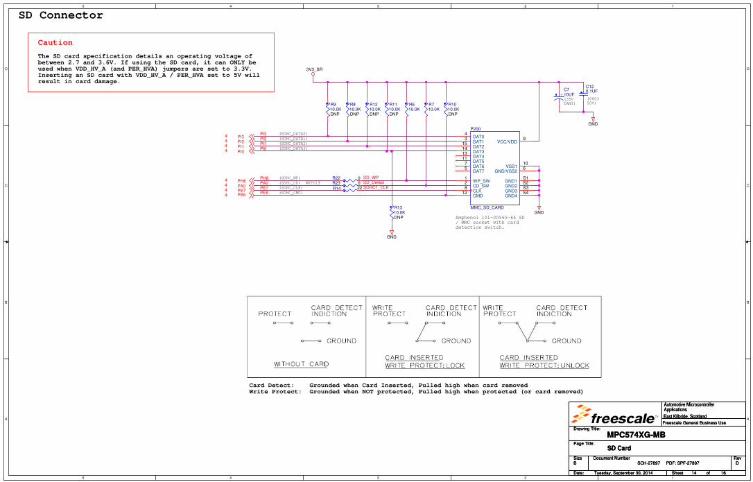
SD Connector
(SDHC_CLK)(SDHC_CMD)
(SDHC_DATA0)(SDHC_DATA1)(SDHC_DATA2)(SDHC_DATA3)
(35VTANT)
Amphenol 101-00565-64 SD/ MMC socket with carddetection switch.
The SD card specification details an operating volt age ofbetween 2.7 and 3.6V. If using the SD card, it can ONLY beused when VDD_HV_A (and PER_HVA) jumpers are set to 3.3V.Inserting an SD card with VDD_HV_A / PER_HVA set to 5V willresult in card damage.
Card Detect: Grounded when Card Inserted, Pulled high when card removedWrite Protect: Grounded when NOT protected, Pulled high when protected (or card removed)
(SDHC_CD) WKPU19(SDHC_WP)
Caution
(060350V)
PE6PE7
PI1
PI3PI2
SDHC1_CLKSD_DetectPA0
SD_WPPH8
PI0
GND
GND
GND
3V3_SR
PE74
PH84
PA04
PE64
PI34
PI24
PI14
PI04
Drawing Title:
Size Document Number Rev
Date: Sheet of
Page Title:
Automotive MicrocontrollerApplications
East Kilbride, Scotland
SCH-27897 PDF: SPF-27897 D
MPC574XG-MB
B
Tuesday, September 30, 2014
SD Card
14 16
Freescale General Business Use
Drawing Title:
Size Document Number Rev
Date: Sheet of
Page Title:
Automotive MicrocontrollerApplications
East Kilbride, Scotland
SCH-27897 PDF: SPF-27897 D
MPC574XG-MB
B
Tuesday, September 30, 2014
SD Card
14 16
Freescale General Business Use
Drawing Title:
Size Document Number Rev
Date: Sheet of
Page Title:
Automotive MicrocontrollerApplications
East Kilbride, Scotland
SCH-27897 PDF: SPF-27897 D
MPC574XG-MB
B
Tuesday, September 30, 2014
SD Card
14 16
Freescale General Business Use
R1210.0KDNP
R610.0K
R1010.0KDNP
R910.0KDNP
R22 0
R710.0K
C120.1UF
+C710UF
P200
MMC_SD_CARD
WP_SW1
CD_SW2
DAT13 DAT04
DAT75
GND/VSS26DAT6
7
CLK8
VCC/VDD9
VSS110DAT5
11
CMD12
DAT413 DAT314 DAT215
GND1S1
GND2S2
GND3S3
GND4S4
R1110.0KDNP
R810.0KDNP
R1310.0KDNP
R23 0
R14 22

5
5
4
4
3
3
2
2
1
1
D D
C C
B B
A A
The LED's, Hex switches and push-button switches ar econnected to MCU pads vvia zero ohm links. If desir edthese can be removed and direct connection made to theLED or switch. All of the ports used for LED's /Switches are also bonded out to the GPIO matrix
Hex Encoded Switch (Active High)
Switches are hard wired to 3.3V rather than 5V so i t's not possible to drive 5V into a 3.3V pad (which would cause damage)Similarly, the LED's are active low with 3.3v suppl y so can be safely coupled to pads on either 3.3V o r 5V domainsThe ADC input is limited to 3.3V, again to prevent driving 5V into a 3.3V pad which would cause damage
PG[2..5] share eMIOS1UC[11..14] with PWMfunctionality
(eMIOS H / X)(eMIOS G / X)(eMIOS G / Y)(eMIOS G)
User Pushbutton Switches (Active High)
User Peripherals, Audio Controls and GPIO
LED's are SMD (1206) Yellow
User LED's (Active Low)
OMRON B3WN-6002 Pushbutton Switch
Since the Hex switch alwayshas an active output, thejumper is to allow the switchto be powered off
ADC Input Pot and Test Point
(Note - This is run from linear 3.3v regulator toprovide a stable input voltage)
(ADC1_P[0])
(0603 50V)
Note - PA1 is also the NMI pin!
Note that LED2 and LED4 (PG3and PG5) can be controlled inLPU_RUN mode (and also have padkeepers in LPU_STANDBY)
PB_SW1PB_SW2
USR_LED4
PB_SW3PB_SW4
USR_LED2USR_LED1
USR_LED3
PA1PA2PF9PF11
HEX_SW1
HEX_SW2
HEX_SW3
PD0
PD1
PD2
PD3HEX_SW4
PG2PG3PG4PG5
PB4
GND
3V3_SR
3V3_SR
3V3_SR
GND
3V3_LR
GND
GND
PG24,12,16
PG34,12,16
PG44,12,16
PG54,12,16
PA2 4,16
PF9 4,16
PF11 4,16
PD1 4,16
PD2 4,16
PD3 4,16
PD0 4,16
PA1 4,16
PB4 4
Drawing Title:
Size Document Number Rev
Date: Sheet of
Page Title:
Automotive MicrocontrollerApplications
East Kilbride, Scotland
SCH-27897 PDF: SPF-27897 D
MPC574XG-MB
B
Tuesday, September 30, 2014
User Peripherals, Audio Controls and GPIO
15 16
Freescale General Business Use
Drawing Title:
Size Document Number Rev
Date: Sheet of
Page Title:
Automotive MicrocontrollerApplications
East Kilbride, Scotland
SCH-27897 PDF: SPF-27897 D
MPC574XG-MB
B
Tuesday, September 30, 2014
User Peripherals, Audio Controls and GPIO
15 16
Freescale General Business Use
Drawing Title:
Size Document Number Rev
Date: Sheet of
Page Title:
Automotive MicrocontrollerApplications
East Kilbride, Scotland
SCH-27897 PDF: SPF-27897 D
MPC574XG-MB
B
Tuesday, September 30, 2014
User Peripherals, Audio Controls and GPIO
15 16
Freescale General Business Use
R286
100
R257 270
DS3AC
R277 0
R275 0
R269 270DS8AC
R262 0
R278 10.0K
R258 0
RV1 2K13
2
SW3
1 2
R290 10.0K
C25 0.1UF
DNP
R287 0
R261 270
P22HDR 1X4DNP
1 2 3 4
R289 0
R276 10.0K
R304 0
R301 10.0K
DS7AC
P20HDR 1X4DNP
1 2 3 4
R282 0
DS2AC
R280 0
R281 10.0K
TP18
1
R303 10.0K
R259 270
R260 0
P19HDR 1X4DNP
1 2 3 4
SW4
1 2
R270 0
SW6
1 2
R302 0
0
35
12
46
7
89A
B C DE
F
SW2
DRS4016
C1
2
8
4
R279 10.0K
SW7
1 2
R288 10.0K
J26
12
J17
12

5
5
4
4
3
3
2
2
1
1
D D
C C
B B
A A
All pads are DNP (Do Not Populate) 0.1" pitch heade rs placed on a 0.1" gridGPIO Pin MatrixPORTA PORTB PORTC PORTD PORTE PORTF PORTG PORTH
PORTQ
Layout Notes: Pads must be placed in a 13 x 16 matrix pattern, 2.54 mm pitch - 13 wide (one column for each port EXCLUDING those with no available pads ie C, E, H, Q) - 16 tall (1 row for each port number from 0 to 15). - GND pad at bottom of each colum - After production, pads should be through hole (not solder filled)
No spare pinson PortQ
No spare pinson PortE
PORTI PORTJ PORTK PORTL PORTM PORTN PORTO PORTP
No spare pinson PortE
Busses are not usedon ports as it makesit harder to seewhich pins are sharedwith other functions
14 GND Pads(one atbottom ofeach colum)
PD[0..3] shared withHex Switch
PD[4..8] shared with TWRPI connector withpullup on PD[7], PD[8]
PA[1,2] shared with user switches
PA[12..15] shared with SAI Audio and TWRPI
PD[13] shared with SAI Audio and MLBheaders
PI[12,13] shared withMLB header
PK[0..4] shared withTWRPI header
PF[9,11] shared withuser switches
PG[2..5] shared withuser LED's, SAI andTWRPI headers
PM[3..4] shared withSAI Audio header
PO[0..1] shared withTWRPI header
PK0PK1
PK3PK2
PK4
PK7PK8PK9
PK11PK10
PK12PK13PK14PK15
PL0PL1
PI9
PI10
PI12
PI13
PJ4
PJ9
PJ11
PJ10
PJ12
PJ15
PK0
PK1
PK3
PK2
PK4
PK7
PK8
PK9
PK11
PK10
PK12
PK13
PK14
PK15
PL0
PL1
PM3
PM4
PM5
PM6
PM11
PM12
PM13
PM14
PM15
PN0
PN1
PN3
PN2
PN4
PN5
PN7
PN6
PN8
PN9
PN11
PN10
PN12
PN15
PO0
PO1
PO3
PO2
PO4
PO5
PO7
PO6
PO8
PO9
PO11
PO10
PO12
PO13
PO14
PO15
PP0
PP1
PP3
PP2
PP4
PP5
PP7
PP6
PP8
PP9
PP11
PP10
PA1
PA2
PA4
PA12
PA13
PA14
PA15
PB5
PB7
PB6
PB11
PB12
PD0
PD1
PD3
PD2
PD4
PD5
PD7
PD6
PD8
PD9
PD11
PD10
PD12
PD13
PF8
PF9
PF11
PF10
PF12
PF13
PG3
PG2
PG4
PG5
PG7
PG6
PG8
PA1PA2PA4
PG3PG2
PG4PG5
PG7PG6
PG8
PA12PA13PA14PA15
PI9PI10
PI12PI13
PB5
PB7PB6
PB11PB12
PF8PF9
PF11PF10
PF12PF13
PJ4
PJ9
PJ11PJ10
PJ12
PJ15
PN13
PN14
PJ13
PJ13PJ14
PJ14
PK5
PK6
PK5PK6
PD0PD1
PD3PD2
PD4PD5
PD7PD6
PD8PD9
PD11PD10
PD12PD13
PM3PM4PM5PM6PM11PM12PM13PM14PM15
PN0PN1
PN3PN2
PN4PN5
PN7PN6
PN8PN9
PN11PN10
PN12
PN15
PN13PN14
PO0PO1
PO3PO2
PO4PO5
PO7PO6
PO8PO9
PO11PO10
PO12PO13PO14PO15
PP0PP1
PP3PP2
PP4PP5
PP7PP6
PP8PP9
PP11PP10
PJ5
PJ6
PJ7
PJ8
PJ5PJ6PJ7PJ8
PH15
PH14
PH13
PH13PH14PH15
PH3PH4PH5
PH5
PH4
PH3
GND
PJ44
PJ94
PJ104
PJ114
PJ124
PJ154
PK04,12
PK14,12
PK24,12
PK34,12
PK44,12
PK74
PK84
PK94
PK104
PK114
PK124
PK134
PK144
PK154
PL04
PL14
PA14,15
PA24,15
PA44
PA124,12
PA134,12
PA144,12
PA154,12
PB54
PB64
PB74
PB114
PB124
PI94
PI104
PI124,13
PI134,13
PJ134
PJ144
PK54
PK64
PD04,15
PD14,15
PD24,15
PD34,15
PD44,12
PD54,12
PD64,12
PD74,12
PD84,12
PD94
PD104
PD114
PD124
PD134,12,13
PJ54
PJ64
PJ74
PJ84
PG2 4,12,15
PG3 4,12,15
PG4 4,12,15
PG5 4,12,15
PG6 4
PG7 4
PG8 4
PF8 4
PF9 4,15
PF10 4
PF11 4,15
PF12 4
PF13 4
PM3 4,12
PM4 4,12
PM5 4
PM6 4
PM11 4
PM12 4
PM13 4
PM14 4
PM15 4
PN0 4
PN1 4
PN2 4
PN3 4
PN4 4
PN5 4
PN6 4
PN7 4
PN8 4
PN9 4
PN10 4
PN11 4
PN12 4
PN13 4
PN14 4
PN15 4
PO0 4,12
PO1 4,12
PO2 4
PO3 4
PO4 4
PO5 4
PO6 4
PO7 4
PO8 4
PO9 4
PO10 4
PO11 4
PO12 4
PO13 4
PO14 4
PO15 4
PP0 4
PP1 4
PP2 4
PP3 4
PP4 4
PP5 4
PP6 4
PP7 4
PP8 4
PP9 4
PP10 4
PP11 4
PH13 4
PH14 4
PH15 4
PH3 4
PH4 4
PH5 4
Drawing Title:
Size Document Number Rev
Date: Sheet of
Page Title:
Automotive MicrocontrollerApplications
East Kilbride, Scotland
SCH-27897 PDF: SPF-27897 D
MPC574XG-MB
B
Tuesday, September 30, 2014
GPIO Pin Matrix
16 16
Freescale General Business Use
Drawing Title:
Size Document Number Rev
Date: Sheet of
Page Title:
Automotive MicrocontrollerApplications
East Kilbride, Scotland
SCH-27897 PDF: SPF-27897 D
MPC574XG-MB
B
Tuesday, September 30, 2014
GPIO Pin Matrix
16 16
Freescale General Business Use
Drawing Title:
Size Document Number Rev
Date: Sheet of
Page Title:
Automotive MicrocontrollerApplications
East Kilbride, Scotland
SCH-27897 PDF: SPF-27897 D
MPC574XG-MB
B
Tuesday, September 30, 2014
GPIO Pin Matrix
16 16
Freescale General Business Use
TPH10
1
IOM921
IOM401
IOM1181
IOM1011
IOM11
IOM721
IOM451
IOM561
IOM181
IOM441
TPH7
1
IOM1111
TPH4
1IOM17
1
IOM701
IOM761
IOM771
IOM391
IOM1021
IOM1311
IOM841
IOM331
IOM71
IOM1241
IOM971
IOM151
IOM961
IOM131
IOM291
IOM991
TPH15
1
IOM191
IOM501
IOM101
IOM811
TPH12
1
IOM581
IOM91
IOM1261
IOM541
IOM881
IOM1281
IOM981
IOM431
IOM261
IOM521
IOM1051
IOM651
IOM241
IOM1041
TPH9
1
IOM461
IOM671
IOM481
IOM911
IOM61
IOM211
IOM891
IOM1231
IOM51
TPH6
1
IOM1031
IOM731
IOM281
TPH3
1
IOM1091
IOM621
IOM631
IOM1151
IOM411
IOM41
IOM531
IOM851
IOM1191
IOM1061
IOM901
IOM321
IOM951
IOM161
IOM341
IOM831
IOM601
IOM1081
IOM511
IOM141
IOM821
IOM871
IOM81
TPH14
1
IOM1161
IOM271
IOM381
IOM801
IOM351
TPH11
1
IOM1211
IOM491
IOM1101
TPH8
1
IOM1291
IOM311
IOM21
IOM1121
IOM781
IOM791
IOM1071
IOM251
IOM691
IOM751
IOM1301
IOM931
IOM941
IOM1321
IOM421
IOM1141
IOM371
IOM591
TPH5
1
IOM301
IOM1251
IOM201
IOM471
IOM641
IOM121
TPH2
1
IOM31
IOM1271
IOM1001
IOM1171
IOM1131
IOM361
IOM711
IOM111
IOM611
IOM681
IOM1221
IOM661
IOM571
TPH13
1
IOM551
IOM741
IOM231
IOM861
IOM221
IOM1201


![1 195.337 mb 195.338 mb 2kb 195.339 mb 195.34 mb o z o U ... · 195.337 mb 195.338 mb 2kb 195.339 mb 195.34 mb o z o U.] U.] Thiel Hey 1 80.836 80.838 mb 80.84 80.842 mb Figure S7](https://img.pdfslide.net/doc/110x75/5e71a866b2da8320f30922bc/1-195337-mb-195338-mb-2kb-195339-mb-19534-mb-o-z-o-u-195337-mb-195338.jpg)


![Customer Service Action Plan [PDF - 3 MB]](https://img.pdfslide.net/doc/110x75/587cb03e1a28ab71378b9148/customer-service-action-plan-pdf-3-mb.jpg)