Embed Size (px)
Citation preview

© Freescale Semiconductor, Inc., 2007. All rights reserved.
Preliminary—Subject to Change Without Notice
Freescale Semiconductor
The MPC8379E-RDB reference design platform is a system featuring the powerful PowerQUICC™ II Pro processor, which includes a built-in security accelerator. This low-cost, high-performance system solution consists of a printed circuit board (PCB) assembly known asthe MPC8379E-RDB Board, a hard disk, plus a board support package (BSP), distributed in a CD image. This BSP enables fastest possible time-to-market for development or integration of applications including media servers, network attached storage devices, and next-generation small office home office/small medium business gateways.
Section 1, “MPC8379E-RDB Board,” describes the board in terms of its hardware: the features, specifications, block diagram, connectors, interface specification, and hardware straps.
Section 2, “Getting Started,” describes the board settings and physical connections needed to boot the MPC8379E-RDB board.
Section 3, “MPC8379E-RDB Software,” describes the software that is shipped with the platform.
Use this manual in conjunction with the following documents:
• MPC8379E PowerQUICC™ II Pro Integrated Host Processor Family Reference Manual (MPC8379ERM)
Document Number: MPC8379ERDBUGRev. 1,8/2007
Contents1. MPC8379E-RDB Board . . . . . . . . . . . . . . . . . . . . . . . 22. Getting Started . . . . . . . . . . . . . . . . . . . . . . . . . . . . . 343. MPC8379E-RDB Software . . . . . . . . . . . . . . . . . . . . 394. Revision History . . . . . . . . . . . . . . . . . . . . . . . . . . . . 40
MPC8379E-RDB Reference Design Platform User’s Guide
WARNINGThis is a class A product. In a domestic environment this product may cause radio interference in which case the user may be required to take adequate measures.
NOTEThis equipment has been tested and found to comply with the limits for a Class A digital device, pursuant to Part 15 of the FCC Rules. These limits are designed to provide reasonable protection against harmful interference when the equipment is operated in a commercial environment. This equipment generates, uses, and can radiate radio frequency energy and, if not installed and used in accordance with the instruction manual, may cause harmful interference to radio communications. Operation of this equipment in a residential area is likely to cause harmful interference in which case the user will be required to correct the interference at his own expense.
MPC8379E-RDB Reference Design Platform User’s Guide, Rev. 1
2 Freescale Semiconductor Preliminary—Subject to Change Without Notice
MPC8379E-RDB Board
• MPC8379E PowerQUICC II Pro Integrated Host Processor Hardware Specifications (MPC8379EEC)
• Hardware and Layout Design Considerations for DDR Memory Interfaces (AN2582)
• MC9S08QG8 Data Sheet
1 MPC8379E-RDB BoardThis section presents the features and block diagram, specifications, and mechanical data for the MPC8379E-RDB board.
1.1 FeaturesThis section presents the features, specification, and block diagram of the MPC8379E-RDB board. The features are as follows:
• CPU
— Freescale MPC8377E / MPC8379E @ 667 MHz
• Memory subsystem
— On board 256-MByte DDR2 unbuffered SDRAM
— 8-MByte NOR Flash
— 32-MBytes NAND Flash
• Interfaces
— 10/100/1000 BaseT Ethernet ports
– eTSEC1
– RGMII interface: 1 x 10/100/1000 BaseT with RJ-45 interface, using RealtekTM RTL8211B single port 10/100/1000 BaseT PHY
– eTSEC 2
– RGMII interface: 5 x 10/100/1000 BaseT with RJ-45 interface, using VitesseTM VSC7385 5-port L2 Gigabit Ethernet switch
– USB 2.0 Hub or mini USB OTG
– 4 x USB2.0 Type A receptable connector, with Genesys LogicTM GL850A 4-PORT USB 2.0 HUB Controller, or
– One mini-AB USB OTG port
— Serial ATA Controller
– Two (MPC8377E) or four (MPC8379E) standard SATA connectors
— PCI: 32-bit PCI interface up to 66 Mhz
– 1x 32-bit 3.3V PCI slot
– 1x 32-bit 3.3V miniPCI slot

MPC8379E-RDB Reference Design Platform User’s Guide, Rev. 1
Freescale Semiconductor 3 Preliminary—Subject to Change Without Notice
MPC8379E-RDB Board
— PCI Express (MPC8377E only)
– One PCI Express Connector
– One miniPCI Express Connector
— SDHC
– One SDHC Card Connector
— I2C
– I2C connected to DallasTM DS1339 RTC with battery holder and AtmelTM AT24C08 Serial EEPROM
— Freescale MC9S08QG8 MCU (20-MHz HCS08 CPU) for fan control and soft start
– Support for Low Power / Wake on LAN. This can be MCU controlled or logic.
— Board Connectors
– 2 X 10 ATX Power supply connector
– RS-232C connectors
• 2x 9 pin DB9 receptables
• Extra header for Bluetooth / Zigbee future connectivity
– JTAG / COP for debugging
– Jumper Clock Mode configurability
— Form factor
– Mini-ITX form factor (170 mm x 170 mm, or 6692 mils x 6692 mils)
• 6-layer PCB (4 layers signals, 2 layer power and ground) routing
• Certification
— CE / FCC
• Lead-Free (ROHS)
MPC8379E-RDB Reference Design Platform User’s Guide, Rev. 1
4 Freescale Semiconductor Preliminary—Subject to Change Without Notice
MPC8379E-RDB Board
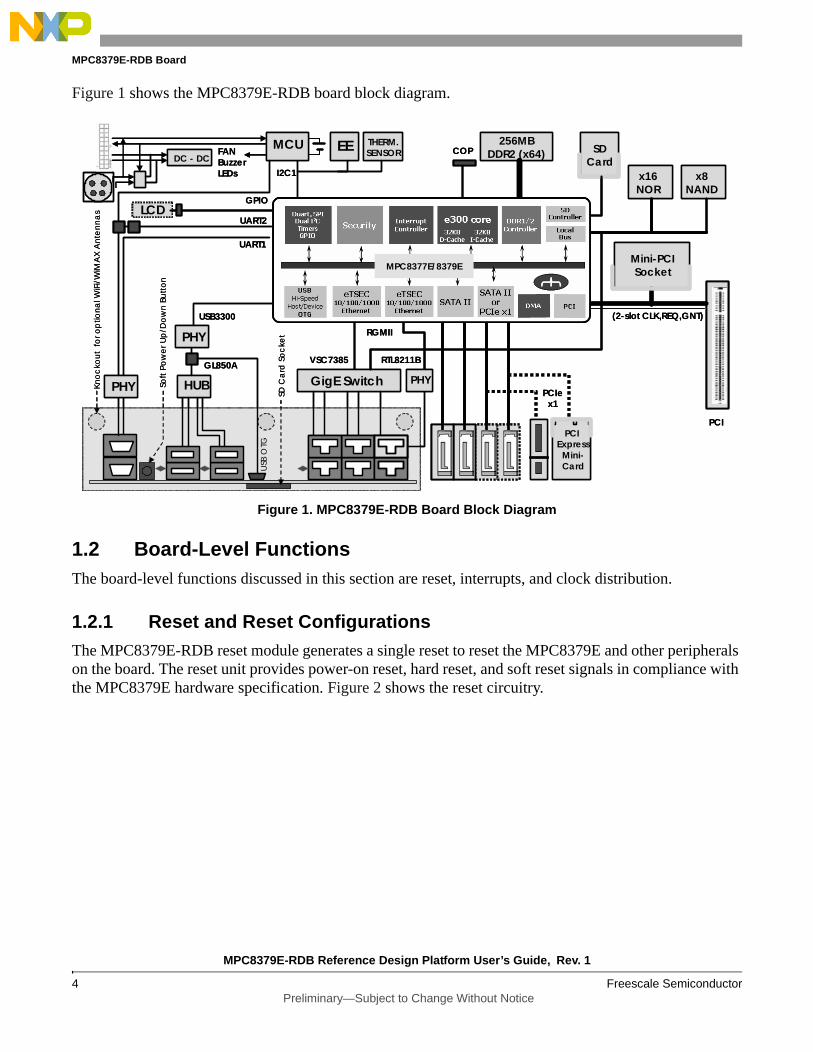
Figure 1 shows the MPC8379E-RDB board block diagram.
Figure 1. MPC8379E-RDB Board Block Diagram
1.2 Board-Level FunctionsThe board-level functions discussed in this section are reset, interrupts, and clock distribution.
1.2.1 Reset and Reset Configurations
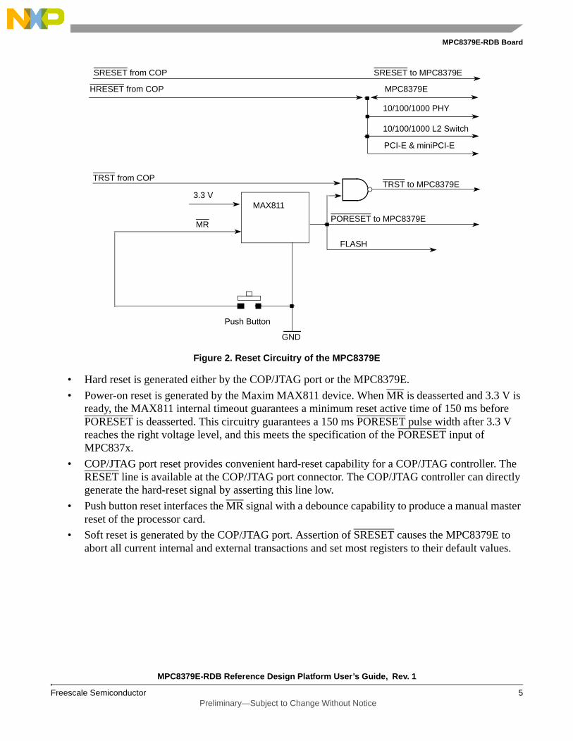
The MPC8379E-RDB reset module generates a single reset to reset the MPC8379E and other peripherals on the board. The reset unit provides power-on reset, hard reset, and soft reset signals in compliance with the MPC8379E hardware specification. Figure 2 shows the reset circuitry.
GigE SwitchHUB
x16NOR
Mini-PCISocket
256MBDDR2 (x64)
LCD
UART1
GPIO
RGMIIPHY
COP
PCI
VSC7385 RTL8211BGL850A
USB3300
I2C1
FANBuzzerLEDs
MCUDC - DC
x8NAND
PHY
SDCard
EE THERM.SENSOR
MPC8377E/8379E
PCI Express
Mini-Card
PCIex1
UART2
PHYKn
oc
kou
t f
or o
ptio
na
l WiF
i/W
iMA
XA
nte
nn
as
SD C
ard
So
cke
t
USB
OTG
Soft
Po
we
r U
p/D
ow
n B
utt
on
(2-slot CLK,REQ,GNT)
MPC8379E-RDB Reference Design Platform User’s Guide, Rev. 1
Freescale Semiconductor 5 Preliminary—Subject to Change Without Notice
MPC8379E-RDB Board
Figure 2. Reset Circuitry of the MPC8379E
• Hard reset is generated either by the COP/JTAG port or the MPC8379E.
• Power-on reset is generated by the Maxim MAX811 device. When MR is deasserted and 3.3 V is ready, the MAX811 internal timeout guarantees a minimum reset active time of 150 ms before PORESET is deasserted. This circuitry guarantees a 150 ms PORESET pulse width after 3.3 V reaches the right voltage level, and this meets the specification of the PORESET input of MPC837x.
• COP/JTAG port reset provides convenient hard-reset capability for a COP/JTAG controller. The RESET line is available at the COP/JTAG port connector. The COP/JTAG controller can directly generate the hard-reset signal by asserting this line low.
• Push button reset interfaces the MR signal with a debounce capability to produce a manual master reset of the processor card.
• Soft reset is generated by the COP/JTAG port. Assertion of SRESET causes the MPC8379E to abort all current internal and external transactions and set most registers to their default values.
MAX8113.3 V
MR
Push Button
HRESET from COP
SRESET from COP
TRST from COP
SRESET to MPC8379E
PORESET to MPC8379E
FLASH
10/100/1000 PHY
MPC8379E
PCI-E & miniPCI-E
10/100/1000 L2 Switch
TRST to MPC8379E
GND
MPC8379E-RDB Reference Design Platform User’s Guide, Rev. 1
6 Freescale Semiconductor Preliminary—Subject to Change Without Notice
MPC8379E-RDB Board
1.2.2 External Interrupts
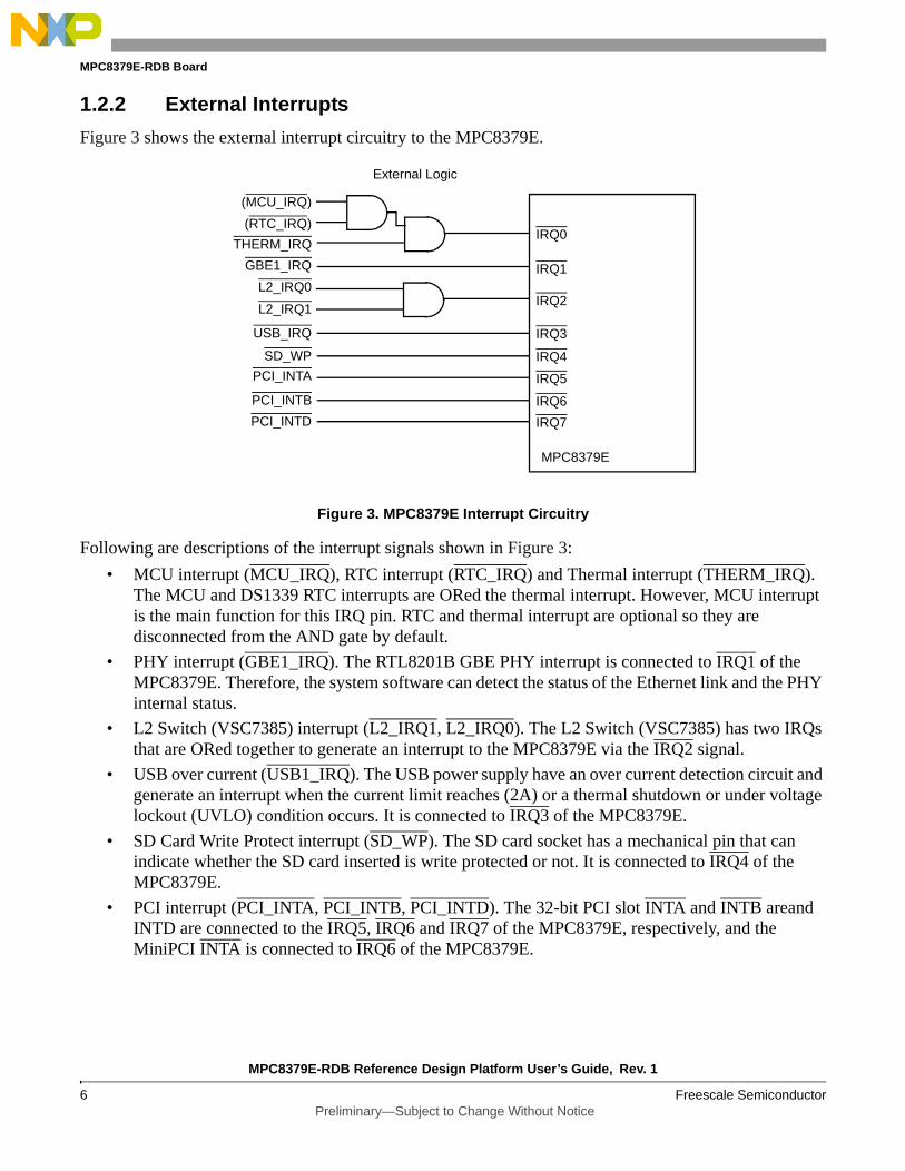
Figure 3 shows the external interrupt circuitry to the MPC8379E.
Figure 3. MPC8379E Interrupt Circuitry
Following are descriptions of the interrupt signals shown in Figure 3:
• MCU interrupt (MCU_IRQ), RTC interrupt (RTC_IRQ) and Thermal interrupt (THERM_IRQ). The MCU and DS1339 RTC interrupts are ORed the thermal interrupt. However, MCU interrupt is the main function for this IRQ pin. RTC and thermal interrupt are optional so they are disconnected from the AND gate by default.
• PHY interrupt (GBE1_IRQ). The RTL8201B GBE PHY interrupt is connected to IRQ1 of the MPC8379E. Therefore, the system software can detect the status of the Ethernet link and the PHY internal status.
• L2 Switch (VSC7385) interrupt (L2_IRQ1, L2_IRQ0). The L2 Switch (VSC7385) has two IRQs that are ORed together to generate an interrupt to the MPC8379E via the IRQ2 signal.
• USB over current (USB1_IRQ). The USB power supply have an over current detection circuit and generate an interrupt when the current limit reaches (2A) or a thermal shutdown or under voltage lockout (UVLO) condition occurs. It is connected to IRQ3 of the MPC8379E.
• SD Card Write Protect interrupt (SD_WP). The SD card socket has a mechanical pin that can indicate whether the SD card inserted is write protected or not. It is connected to IRQ4 of the MPC8379E.
• PCI interrupt (PCI_INTA, PCI_INTB, PCI_INTD). The 32-bit PCI slot INTA and INTB areand INTD are connected to the IRQ5, IRQ6 and IRQ7 of the MPC8379E, respectively, and the MiniPCI INTA is connected to IRQ6 of the MPC8379E.
GBE1_IRQ
(RTC_IRQ)
USB_IRQ
SD_WP
L2_IRQ0
L2_IRQ1
THERM_IRQ
PCI_INTA
PCI_INTB
IRQ1
IRQ2
IRQ3
IRQ4
IRQ5
IRQ6
IRQ7
MPC8379E
External Logic
(MCU_IRQ)
PCI_INTD
IRQ0

MPC8379E-RDB Reference Design Platform User’s Guide, Rev. 1
Freescale Semiconductor 7 Preliminary—Subject to Change Without Notice
MPC8379E-RDB Board
1.2.3 Clock Distribution
Figure 4 and Table 1 show the clock distribution on the MPC8379E-RDB board.
Figure 4. MPC8379E-RDB Clock Scheme
MPC8379E
Local Bus CLK
DDR2 SDRAM
LCLKx
MCKx
DS1339
GND GND
16 KHzCrystal
MCKx
200 MHz
50 MHz to 133 MHz
eTSEC
local bus
DLL
DDRDLL
PCIDIV
66.666 MHz
OSC
CLKIN
33/66 MHz
33/66 MHz
32-bit PCI Slot
Mini PCI SlotOCCR
2PCI_SYNC_OUT
PCI_SYNC_INSystem
PLL
CFG_CLKIN_DIV
USB3300
GND GND
24 MHzCrystal
GL850A
GND GND
12 MHzCrystal
25 MHz
OSC
RTL8211B
VSC7385
125 MHz
OSC125 MHz
M66EN
CLK (DDR400)
MPC8379E-RDB Reference Design Platform User’s Guide, Rev. 1
8 Freescale Semiconductor Preliminary—Subject to Change Without Notice
MPC8379E-RDB Board
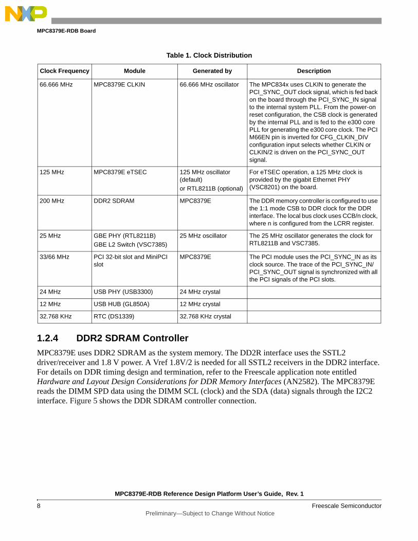
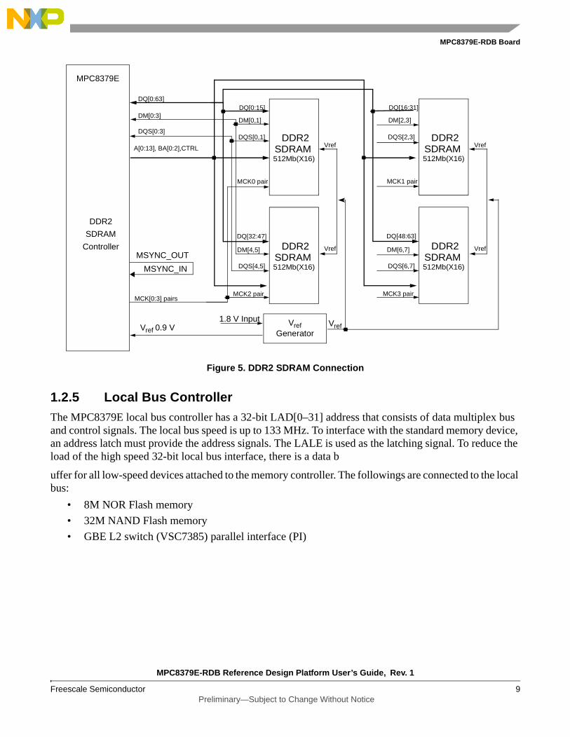
1.2.4 DDR2 SDRAM ControllerMPC8379E uses DDR2 SDRAM as the system memory. The DD2R interface uses the SSTL2 driver/receiver and 1.8 V power. A Vref 1.8V/2 is needed for all SSTL2 receivers in the DDR2 interface. For details on DDR timing design and termination, refer to the Freescale application note entitled Hardware and Layout Design Considerations for DDR Memory Interfaces (AN2582). The MPC8379E reads the DIMM SPD data using the DIMM SCL (clock) and the SDA (data) signals through the I2C2 interface. Figure 5 shows the DDR SDRAM controller connection.
Table 1. Clock Distribution
Clock Frequency Module Generated by Description
66.666 MHz MPC8379E CLKIN 66.666 MHz oscillator The MPC834x uses CLKIN to generate the PCI_SYNC_OUT clock signal, which is fed back on the board through the PCI_SYNC_IN signal to the internal system PLL. From the power-on reset configuration, the CSB clock is generated by the internal PLL and is fed to the e300 core PLL for generating the e300 core clock. The PCI M66EN pin is inverted for CFG_CLKIN_DIV configuration input selects whether CLKIN or CLKIN/2 is driven on the PCI_SYNC_OUT signal.
125 MHz MPC8379E eTSEC 125 MHz oscillator (default)or RTL8211B (optional)
For eTSEC operation, a 125 MHz clock is provided by the gigabit Ethernet PHY (VSC8201) on the board.
200 MHz DDR2 SDRAM MPC8379E The DDR memory controller is configured to use the 1:1 mode CSB to DDR clock for the DDR interface. The local bus clock uses CCB/n clock, where n is configured from the LCRR register.
25 MHz GBE PHY (RTL8211B)GBE L2 Switch (VSC7385)
25 MHz oscillator The 25 MHz oscillator generates the clock for RTL8211B and VSC7385.
33/66 MHz PCI 32-bit slot and MiniPCI slot
MPC8379E The PCI module uses the PCI_SYNC_IN as its clock source. The trace of the PCI_SYNC_IN/ PCI_SYNC_OUT signal is synchronized with all the PCI signals of the PCI slots.
24 MHz USB PHY (USB3300) 24 MHz crystal
12 MHz USB HUB (GL850A) 12 MHz crystal
32.768 KHz RTC (DS1339) 32.768 KHz crystal
MPC8379E-RDB Reference Design Platform User’s Guide, Rev. 1
Freescale Semiconductor 9 Preliminary—Subject to Change Without Notice
MPC8379E-RDB Board
Figure 5. DDR2 SDRAM Connection
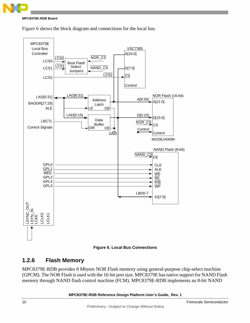
1.2.5 Local Bus ControllerThe MPC8379E local bus controller has a 32-bit LAD[0–31] address that consists of data multiplex bus and control signals. The local bus speed is up to 133 MHz. To interface with the standard memory device, an address latch must provide the address signals. The LALE is used as the latching signal. To reduce the load of the high speed 32-bit local bus interface, there is a data b
uffer for all low-speed devices attached to the memory controller. The followings are connected to the local bus:
• 8M NOR Flash memory
• 32M NAND Flash memory
• GBE L2 switch (VSC7385) parallel interface (PI)
DDR2
SDRAM
Controller
VrefGenerator
Vref 0.9 V1.8 V Input Vref
MSYNC_OUT
MSYNC_IN
MPC8379E
DDR2SDRAM
Vref
Vref
512Mb(X16)
DQ[0:63]
DQ[32:47]
DQ[0:15]DM[0:3]
DM[0,1]
DM[4,5]
DQS[0:3]DQS[0,1]
DQS[4,5]
A[0:13], BA[0:2],CTRL
MCK[0:3] pairs
MCK0 pair
MCK2 pair
DDR2SDRAM512Mb(X16)
DDR2SDRAM512Mb(X16)
DQ[48:63]
DQ[16:31]
DM[2,3]
DM[6,7]
DQS[2,3]
DQS[6,7]
MCK1 pair
MCK3 pair
DDR2SDRAM512Mb(X16)
Vref
Vref
MPC8379E-RDB Reference Design Platform User’s Guide, Rev. 1
10 Freescale Semiconductor Preliminary—Subject to Change Without Notice
MPC8379E-RDB Board
Figure 6 shows the block diagram and connections for the local bus.
Figure 6. Local Bus Connections
1.2.6 Flash Memory
MPC8379E-RDB provides 8 Mbytes NOR Flash memory using general-purpose chip-select machine (GPCM). The NOR Flash is used with the 16-bit port size. MPC8379E has native support for NAND Flash memory through NAND flash control machine (FCM). MPC8379E-RDB implements an 8-bit NAND
A[21:0]
CS
MX29LV640M
NOR Flash (16-bit)
MPC8379E
Control Signals
LAD[0:31]
BADDR[27:29]
D[15:0]
ALE
Address
LE
LBCTL
Local Bus
LCS0
Control
Data
DIR OE
OE
GND
D[0:15]
A[9:30]
LCLK
0
LCLK
1
LCK
E
LSY
NC
_OU
TLS
YN
_IN
NOR_CS
Latch
Buffer
LCS0Boot Flash
Select
NOR_CS
NAND_CS
Control
LAD[8:31]
LAD[0:15]
A[16:0]
CS
VSC7385
D[7:0]
Control
LCS2LCS2
Controller
JumpersLCS1LCS1
CLEALEWE RE R/B WP
GPL0GPL1WE0 GPL2GPL4GPL3
IO[7:0]LBD0-7
NAND Flash (8-bit)
CENAND_CS

MPC8379E-RDB Reference Design Platform User’s Guide, Rev. 1
Freescale Semiconductor 11 Preliminary—Subject to Change Without Notice
MPC8379E-RDB Board
flash with 32/64 MByte in size. Either of the two Flash memory devices can be selected as the boot Flash as shown in Figure 21.
1.2.7 I2CThe MPC8379E has two I2C interfaces. On the MPC8379E-RDB board, the MPC8379E acts as I2C master for both I2C buses (I2C1 and I2C2). I2C1 is connected to:
• Serial EEPROM M24256 at address 0x50.
• PCF8574 I2C expander at address 0x39
• Thermal sensor LM75 at address 0x48.
• Real-time clock DS1339U at address 0x68.
• MCU MC9S08QG8 at address 0x0A.
I2C2 is connected to the clock generater ICS9FG104, PCI-E and mini PCI-E socket.
The M24256 serial EEPROM can be used to store the reset configuration word of the MPC8379E, as well as storing the configuration registers values if boot sequencer of MPC8379E is enabled. If user wants to load the reset configuration word from the I2C1 M24256 EEPROM, the CFG_RST_SRC DIP switch S3 should be set accordingly. For more details on how to program the reset configuration word value in I2C EEPROM and the boot sequencer mode, please refer to the MPC8379ERM. The I2C address of the M24256 EEPROM on I2C1 bus is 0x50.
There is a PCF8574A I2C I/O expander on the MPC8379E-RDB board to provide general purpose I/O expansion via the I2C1 interface. The PCF8574A has I2C1 address 0x39 and it is able to detect the board revision number, detect which flash is currently used to boot, the miniPCI clock run signal level and enable the LCD interface of the MPC8379E-RDB board. The bit defintion of the PCF8574A is defined as in Table 2:
Table 2. PCF8574A Bit Descriptions
PCF8574A (U10) bit[0..7]
Name Read/Write Description
0 REV1 Read only, write has no effect
Board revision numberREV[0:1] definition00: revision 1.001: revision 1.110: reserved11: reserved
1 REV0
2 RSVD1 Read only, write has no effect
Reserved for future use
3 RSVD0 Read only, write has no effect
Reserved for future use

MPC8379E-RDB Reference Design Platform User’s Guide, Rev. 1
12 Freescale Semiconductor Preliminary—Subject to Change Without Notice
MPC8379E-RDB Board
The DS1339 RTC is connected to I2C with address 0x68. The software running on PowerPC core can read or write to the RTC through the I2C1 interface.
1.2.8 GBE L2 Switch (VSC7385) Parallel InterfaceThe GBE L2 switch (VSC7385) parallel interface gives the MPC8379E access to its internal registers through the local bus. The internal 8051 core of the VSC7385 is disabled by default so that the parallel interface is active. The MPC8379E general-purpose chip-select machine (GPCM) generates the timing of read/write accesses. Read/write accesses to the VSC7385 are terminated by the DONE signal, which is connected to the LGTA of the GPCM and generates the internal TA for the PowerPC™ core. Figure 7 shows the connection between the VSC7385 and the MPC8379E.
Figure 7. Parallel Interface of VSC7385
4 BOOT0 Read only, write has no effect
Used to determine which flash is used for boot flash0: NOR Flash is the boot flash1: NAND Flash is the boot flash
5 MPCI_CLKRUN Read/Write MiniPCI clock run signal level, defined by the PCI Mobile Design Guide.0: MiniPCI clock is in normal operating frequency1: MiniPCI clock is stopped or running very low
6 LCD_EN Write only, read returns 1
Enable/disable the LCD interface0: LCD interface is enabled1: LCD interface is disabled
7 Not used — —
Table 2. PCF8574A Bit Descriptions
PCF8574A (U10) bit[0..7]
Name Read/Write Description
A[16:0]
CS
VSC7385
D[7:0]
WR
LCS2
A[15:31]
D[0:7]
OE
Done
WE
GPL2(OE)
GPL4(LGTA)
ICPU_Pi_EnICPU_SI_Boot_En Pull Low
MPC8379E-RDB Reference Design Platform User’s Guide, Rev. 1
Freescale Semiconductor 13 Preliminary—Subject to Change Without Notice
MPC8379E-RDB Board
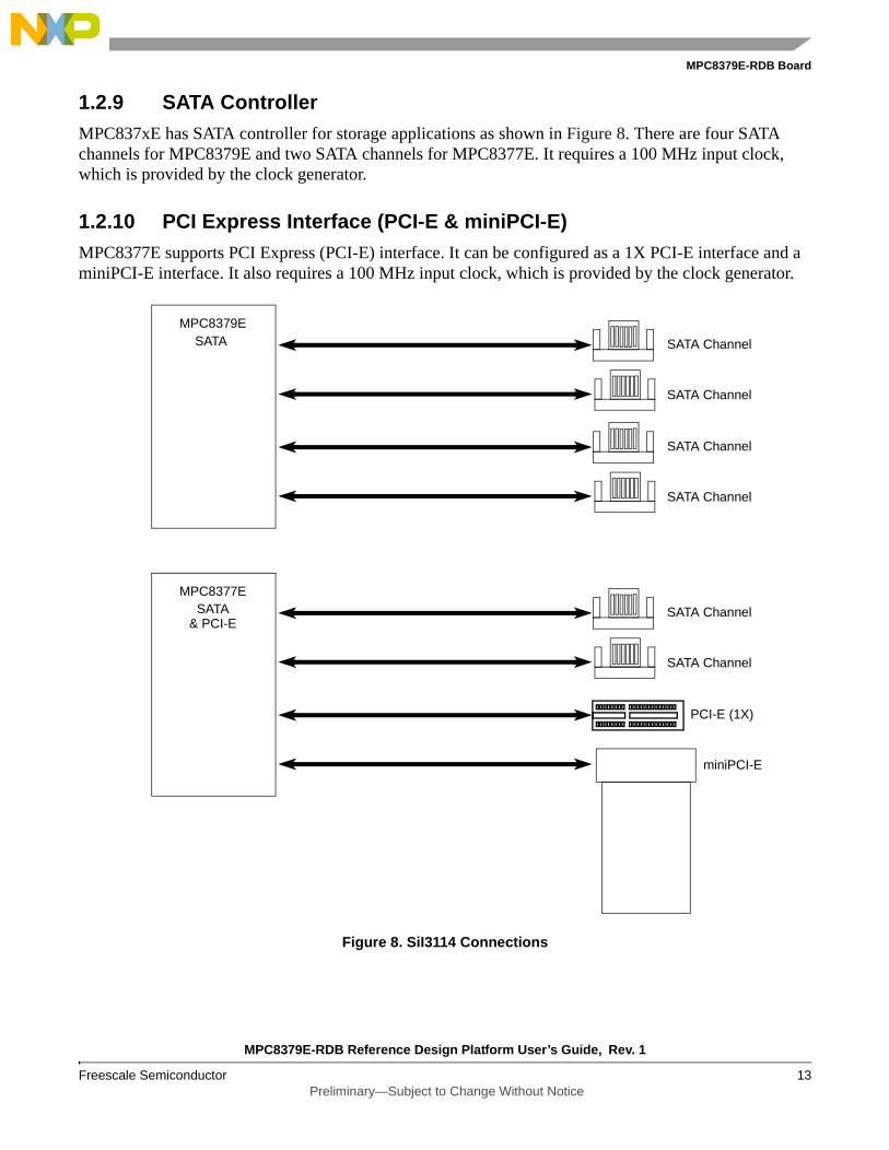
1.2.9 SATA ControllerMPC837xE has SATA controller for storage applications as shown in Figure 8. There are four SATA channels for MPC8379E and two SATA channels for MPC8377E. It requires a 100 MHz input clock, which is provided by the clock generator.
1.2.10 PCI Express Interface (PCI-E & miniPCI-E)MPC8377E supports PCI Express (PCI-E) interface. It can be configured as a 1X PCI-E interface and a miniPCI-E interface. It also requires a 100 MHz input clock, which is provided by the clock generator.
Figure 8. SiI3114 Connections
MPC8379ESATA SATA Channel
SATA Channel
SATA Channel
SATA Channel
MPC8377ESATA SATA Channel
SATA Channel
PCI-E (1X)
miniPCI-E
& PCI-E
MPC8379E-RDB Reference Design Platform User’s Guide, Rev. 1
14 Freescale Semiconductor Preliminary—Subject to Change Without Notice
MPC8379E-RDB Board
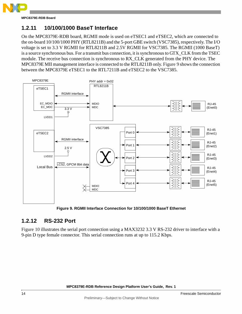
1.2.11 10/100/1000 BaseT InterfaceOn the MPC8379E-RDB board, RGMII mode is used on eTSEC1 and eTSEC2, which are connected to the on-board 10/100/1000 PHY (RTL8211B) and the 5-port GBE switch (VSC7385), respectively. The I/O voltage is set to 3.3 V RGMII for RTL8211B and 2.5V RGMII for VSC7385. The RGMII (1000 BaseT) is a source synchronous bus. For a transmit bus connection, it is synchronous to GTX_CLK from the TSEC module. The receive bus connection is synchronous to RX_CLK generated from the PHY device. The MPC8379E MII management interface is connected to the RTL8211B only. Figure 9 shows the connection between the MPC8379E eTSEC1 to the RTL7211B and eTSEC2 to the VSC7385.
Figure 9. RGMII Interface Connection for 10/100/1000 BaseT Ethernet
1.2.12 RS-232 PortFigure 10 illustrates the serial port connection using a MAX3232 3.3 V RS-232 driver to interface with a 9-pin D type female connector. This serial connection runs at up to 115.2 Kbps.
RJ-45
eTSEC1
MPC8379E
RTL8211B
MDIOMDC
EC_MDIOEC_MDC
RGMII interface
PHY addr = 0x02
eTSEC2
2.5 V
LVDD2
Port 0
Port 1
Port 2
Port 3
Port 4
VSC7385 RJ-45
MDIOMDC
(Enet0)
(Enet1)
RJ-45(Enet2)
RJ-45(Enet3)
RJ-45(Enet4)
RJ-45(Enet5)
3.3 V
LVDD1
RGMII interface
Local BusLCS2, GPCM 8bit data

MPC8379E-RDB Reference Design Platform User’s Guide, Rev. 1
Freescale Semiconductor 15 Preliminary—Subject to Change Without Notice
MPC8379E-RDB Board
Figure 10. UART Debug Port Connection
1.2.13 USB 2.0 InterfaceThe MPC8379E has a internal USB modules (dual-role (DR) module). On the MPC8379E-RDB board, it is connect to USB PHY (USB3300) through the 8-bit UTMI low pin count interface (ULPI). The USB3300 PHY connects to an Mini-AB type receptacle connector that serves as a host/device/OTG USB interface or on-board USB2.0 hub controller (GL850A) to expand the USB interfaces to four USB2.0 host ports by using two jumpers. Table 3 shows the USB port configuration.
Figure 11 shows the connection of USB.
Figure 11. USB Port Connections
Table 3. USB Port Configurations
Jumper JP1, JP2position
Interface Type USB PHY Operating Mode USB Hub Connector Type
PHY [1-2] ULPI USB3300 DR Host/Device/OTG Nil 1 x Type Mini-AB Receptacle
HUB [2-3] ULPI USB3300 MPH Host GL850A 4 x Type B Receptacle
MAX3232
TXD
RXD
CTSRXTX
TX
DO
DI
DIMPC8379E
RTS
DB-9
RS-232SerialPort
RXRXD
RTS
TXD
CTSDO
UART0
MPC8379E
ULPI_D[7:0]
ULPI_STPULPI_NXT
ULPI_CLK
DIR
USB3300
D[7:0]
STPNXTCLKOUT
CPEN
ULPI_DIR
GL850ADPDM
VBUS
USB Type B x 4
MIC2505
VBUS
DMDP
ID
DMx4DPx4
USB Type Mini-AB
5 V
JP1 JP2

MPC8379E-RDB Reference Design Platform User’s Guide, Rev. 1
16 Freescale Semiconductor Preliminary—Subject to Change Without Notice
MPC8379E-RDB Board
1.2.14 PCI SubsystemThe MPC8379E has a PCI interfaces. It connects to a 32-bit 3.3 V PCI slot and a MiniPCI slot, as shown in Figure 12.
Figure 12. PCI Subsystem
1.2.15 MCU SubsystemThe Freescale MC9S08QG8 is a highly integrated, low-power microcontroller that offers 8 Kbyte Flash memory, 512 bytes of SRAM, I2C, SCI, SPI, 10-bit A/D, timers, and on-chip debugging. It can use an external 32.768 KHz crystal oscillator or an internal oscillator (trim-able to +/– 2%), with an on-chip frequency locked loop multiplier to 8 MHz bus clock operation. In this design, it provides push button soft power-up, software-controlled power-down, and fan and LED control. With additional microcontroller firmware, it can provide an I2C real-time clock and EEPROM emulation capability, thermal measurement, IR remote control, and other advanced features. The main connection to the MPC8379E is I2C (1), but an alternative UART (2) connection is also available.
1.2.16 COP/JTAG Port
The common on-chip processor (COP) is part of the MPC8379E JTAG module and is implemented as a set of additional instructions and logic. This port can connect to a dedicated emulator for extensive system debugging. Several third-party emulators in the market can connect to the host computer through the Ethernet port, USB port, parallel port, RS-232, and so on. A typical setup using a USB port emulator is shown in Figure 13.
MPC8379E
32-Bit PCI
PCI-AD[0:31]
PCI-CBE[0:3]
PCI-REQ0
PCI-GNT0
PCI-CTRL 32-Bit 3.3 V
PCI Slot
32-Bit 3.3 V
MiniPCI Slot
PCI-REQ1
PCI-GNT1
AD15
AD14
PCI-REQ3
PCI-GNT2
MPC8379E-RDB Reference Design Platform User’s Guide, Rev. 1
Freescale Semiconductor 17 Preliminary—Subject to Change Without Notice
MPC8379E-RDB Board
Figure 13. Connecting the MPC8379E-RDB Board to A Parallel Emulator
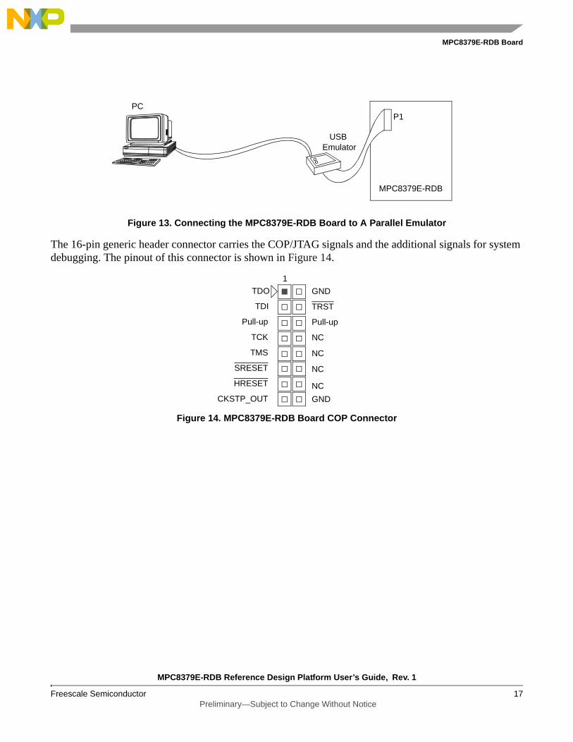
The 16-pin generic header connector carries the COP/JTAG signals and the additional signals for system debugging. The pinout of this connector is shown in Figure 14.
Figure 14. MPC8379E-RDB Board COP Connector
PC
MPC8379E-RDB
P1
USBEmulator
TDI
Pull-up
TCK
TMS
SRESET
HRESET
CKSTP_OUT
GND
TRST
Pull-up
NC
NC
GND
1
TDO
NC
NC
MPC8379E-RDB Reference Design Platform User’s Guide, Rev. 1
18 Freescale Semiconductor Preliminary—Subject to Change Without Notice
MPC8379E-RDB Board
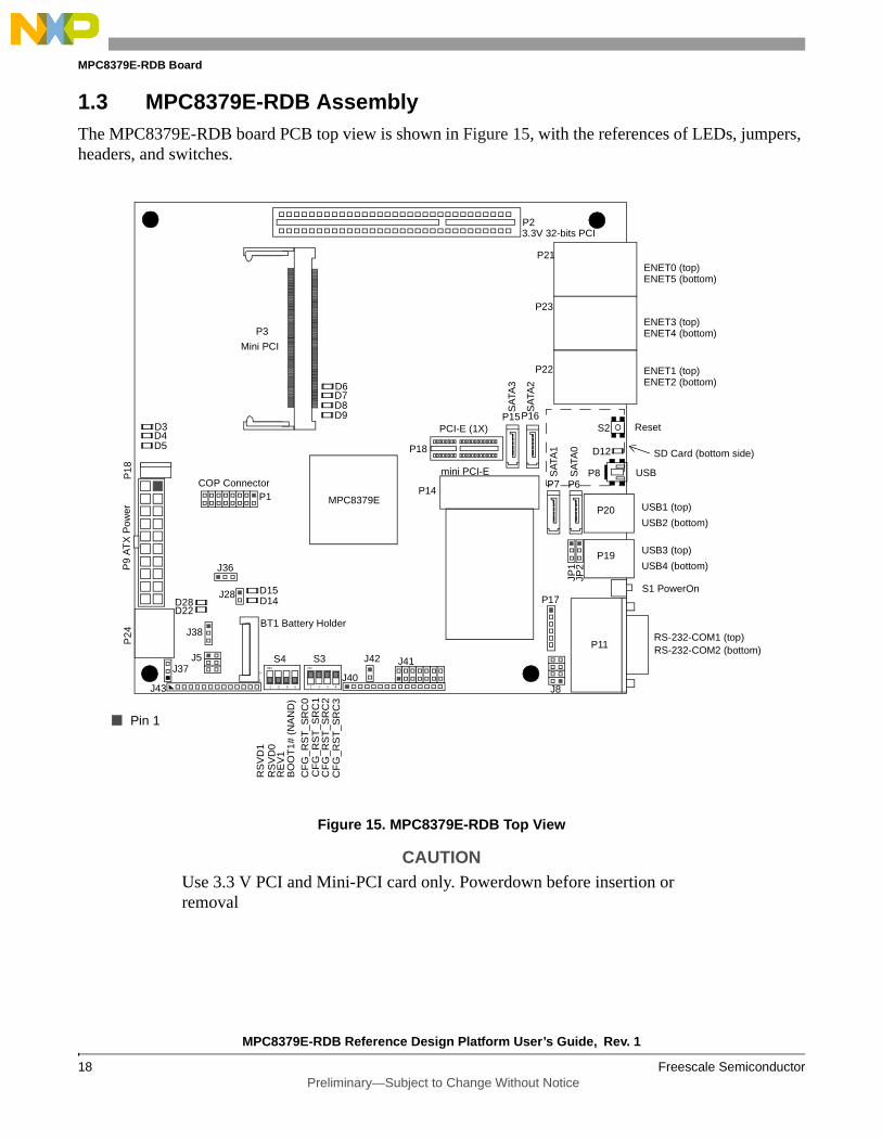
1.3 MPC8379E-RDB AssemblyThe MPC8379E-RDB board PCB top view is shown in Figure 15, with the references of LEDs, jumpers, headers, and switches.
Figure 15. MPC8379E-RDB Top View
CAUTIONUse 3.3 V PCI and Mini-PCI card only. Powerdown before insertion or removal
Pin 1
SA
TA0
RS-232-COM1 (top)
D3
USB
P2
BT1 Battery Holder
D12
P1
USB3 (top)
USB4 (bottom)
USB1 (top)
USB2 (bottom)
ENET1 (top)ENET2 (bottom)
ENET3 (top)ENET4 (bottom)
ENET0 (top)ENET5 (bottom)
Reset
J41
J40
J5
3.3V 32-bits PCI
COP Connector
P22
P23
P21
P20
P19
P8
P15
P7
J8
J42
D15
P16
P6
S1 PowerOn
S2
RS-232-COM2 (bottom)P11
P9
AT
X P
ower
J38
J36
J37
J43
JP2
JP1
J28D14D28
D22
P18
PCI-E (1X)
P18
Mini PCI
P3
SA
TA1
SA
TA2
SA
TA3
mini PCI-E
P14
SD Card (bottom side)
D4D5
S4 S3
CF
G_R
ST
_SR
C0
CF
G_R
ST
_SR
C1
CF
G_R
ST
_SR
C2
CF
G_R
ST
_SR
C3
RS
VD
1R
SV
D0
RE
V1
BO
OT
1# (
NA
ND
)
MPC8379E
P17
P24
D6D7D8D9
1 2 3 4
ON
1 2 3 4
ON
0
1
MPC8379E-RDB Reference Design Platform User’s Guide, Rev. 1
Freescale Semiconductor 19 Preliminary—Subject to Change Without Notice
MPC8379E-RDB Board
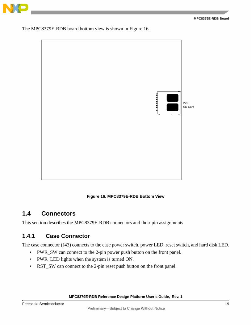
The MPC8379E-RDB board bottom view is shown in Figure 16.
Figure 16. MPC8379E-RDB Bottom View
1.4 ConnectorsThis section describes the MPC8379E-RDB connectors and their pin assignments.
1.4.1 Case ConnectorThe case connector (J43) connects to the case power switch, power LED, reset switch, and hard disk LED.
• PWR_SW can connect to the 2-pin power push button on the front panel.
• PWR_LED lights when the system is turned ON.
• RST_SW can connect to the 2-pin reset push button on the front panel.
P25SD Card

MPC8379E-RDB Reference Design Platform User’s Guide, Rev. 1
20 Freescale Semiconductor Preliminary—Subject to Change Without Notice
MPC8379E-RDB Board
Table 4 lists the pin assignments of the case connector.
1.4.2 COP ConnectorThe COP connector (P1) allows the user to connect a COP/JTAG-based debugger to the MPC8379E-RDB board for debugging. Table 5 lists the pin assignments of the COP connector.
Table 4. Case Connector J10 Pin Assignments
Pin Signal
1 Power LED1 A
2
3 Power LED1 K
4 Power LED1 K
5 Power LED2 A
6
7 Power LED2 K
8 Power LED2 K
9 RESET
10 GND
11 Power On
12 GND
Table 5. COP Connector Pin Assignments
Pin Signal Pin Signal
1 TDO 2 GND
3 TDI 4 TRST
5 QREQ 6 VDD_SENSE
7 TCK 8 CHKSTOP_IN
9 TMS 10 NC
11 SRESET 12 NC
13 HRESET 14 GND

MPC8379E-RDB Reference Design Platform User’s Guide, Rev. 1
Freescale Semiconductor 21 Preliminary—Subject to Change Without Notice
MPC8379E-RDB Board
1.4.3 RS-232C ConnectorsSerial interface COM1 is available at connector P11 (top), and another serial port connection COM2 is available at connector P11 (bottom) or through a 6-pin connector P17 with pin assignment as shown in Table 6.
1.4.4 Serial ATA (SATA) ConnectorsThe SATA connectors (P6, P7, P15, P16) connect to the serial ATA hard disks through serial ATA cables. P6 corresponds to harddisk0, and P7, P16, P15 correspond to harddisk1, harddisk2, and harddisk3, respectively.
1.4.5 PCI SlotThe MPC8379E-RDB board has one 32-bit 3.3 V PCI expansion slot (P2) for an expansion card.
WARNINGOnly the 3.3 V PCI Card is supported. Turn OFF power during insertion and removal of PCI card.
Table 6. COM2 Connector Pin Description
Pin Signal
1 3.3 V
2 GND
3 RTS
4 CTS
5 TXD
6 RXD
MPC8379E-RDB Reference Design Platform User’s Guide, Rev. 1
22 Freescale Semiconductor Preliminary—Subject to Change Without Notice
MPC8379E-RDB Board
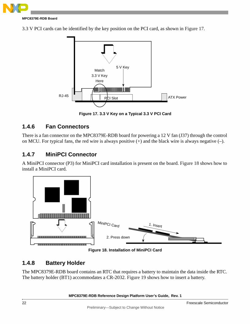
3.3 V PCI cards can be identified by the key position on the PCI card, as shown in Figure 17.
Figure 17. 3.3 V Key on a Typical 3.3 V PCI Card
1.4.6 Fan ConnectorsThere is a fan connector on the MPC8379E-RDB board for powering a 12 V fan (J37) through the control on MCU. For typical fans, the red wire is always positive (+) and the black wire is always negative (–).
1.4.7 MiniPCI ConnectorA MiniPCI connector (P3) for MiniPCI card installation is present on the board. Figure 18 shows how to install a MiniPCI card.
Figure 18. Installation of MiniPCI Card
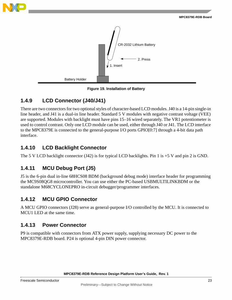
1.4.8 Battery HolderThe MPC8379E-RDB board contains an RTC that requires a battery to maintain the data inside the RTC. The battery holder (BT1) accommodates a CR-2032. Figure 19 shows how to insert a battery.
PCI Slot
5 V Key
ATX PowerRJ-45
Match3.3 V Key
Here
MiniPCI Card 1. Insert
2. Press down
MPC8379E-RDB Reference Design Platform User’s Guide, Rev. 1
Freescale Semiconductor 23 Preliminary—Subject to Change Without Notice
MPC8379E-RDB Board
Figure 19. Installation of Battery
1.4.9 LCD Connector (J40/J41)
There are two connectors for two optional styles of character-based LCD modules. J40 is a 14-pin single-in line header, and J41 is a dual-in line header. Standard 5 V modules with negative contrast voltage (VEE) are supported. Modules with backlight must have pins 15–16 wired separately. The VR1 potentiometer is used to control contrast. Only one LCD module can be used, either through J40 or J41. The LCD interface to the MPC8379E is connected to the general-purpose I/O ports GPIO[0:7] through a 4-bit data path interface.
1.4.10 LCD Backlight ConnectorThe 5 V LCD backlight connector (J42) is for typical LCD backlights. Pin 1 is +5 V and pin 2 is GND.
1.4.11 MCU Debug Port (J5)J5 is the 6-pin dual in-line 68HCS08 BDM (background debug mode) interface header for programming the MC9S08QG8 microcontroller. You can use either the PC-based USBMULTILINKBDM or the standalone M68CYCLONEPRO in-circuit debugger/programmer interfaces.
1.4.12 MCU GPIO ConnectorA MCU GPIO connectors (J28) serve as general-purpose I/O controlled by the MCU. It is connected to MCU1 LED at the same time.
1.4.13 Power ConnectorP9 is compatible with connectors from ATX power supply, supplying necessary DC power to the MPC8379E-RDB board. P24 is optional 4-pin DIN power connector.
Battery Holder
1. Insert
2. Press
CR-2032 Lithium Battery
MPC8379E-RDB Reference Design Platform User’s Guide, Rev. 1
24 Freescale Semiconductor Preliminary—Subject to Change Without Notice
MPC8379E-RDB Board
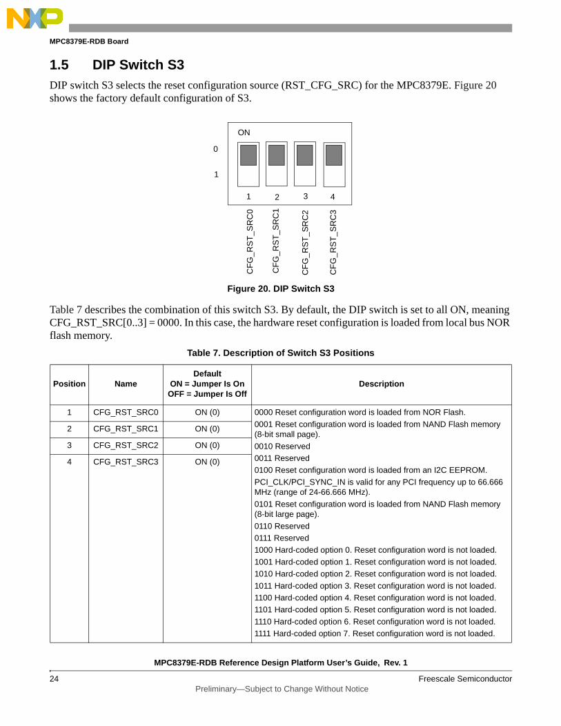
1.5 DIP Switch S3DIP switch S3 selects the reset configuration source (RST_CFG_SRC) for the MPC8379E. Figure 20 shows the factory default configuration of S3.
Figure 20. DIP Switch S3
Table 7 describes the combination of this switch S3. By default, the DIP switch is set to all ON, meaning CFG_RST_SRC[0..3] = 0000. In this case, the hardware reset configuration is loaded from local bus NOR flash memory.
Table 7. Description of Switch S3 Positions
Position NameDefault
ON = Jumper Is OnOFF = Jumper Is Off
Description
1 CFG_RST_SRC0 ON (0) 0000 Reset configuration word is loaded from NOR Flash.
0001 Reset configuration word is loaded from NAND Flash memory (8-bit small page).
0010 Reserved0011 Reserved0100 Reset configuration word is loaded from an I2C EEPROM.
PCI_CLK/PCI_SYNC_IN is valid for any PCI frequency up to 66.666 MHz (range of 24-66.666 MHz).
0101 Reset configuration word is loaded from NAND Flash memory (8-bit large page).
0110 Reserved0111 Reserved1000 Hard-coded option 0. Reset configuration word is not loaded.
1001 Hard-coded option 1. Reset configuration word is not loaded.1010 Hard-coded option 2. Reset configuration word is not loaded.
1011 Hard-coded option 3. Reset configuration word is not loaded.1100 Hard-coded option 4. Reset configuration word is not loaded.1101 Hard-coded option 5. Reset configuration word is not loaded.
1110 Hard-coded option 6. Reset configuration word is not loaded.1111 Hard-coded option 7. Reset configuration word is not loaded.
2 CFG_RST_SRC1 ON (0)
3 CFG_RST_SRC2 ON (0)
4 CFG_RST_SRC3 ON (0)
1 2 3 4
ON
CF
G_R
ST
_SR
C0
0
1
CF
G_R
ST
_SR
C1
CF
G_R
ST
_SR
C2
CF
G_R
ST
_SR
C3

MPC8379E-RDB Reference Design Platform User’s Guide, Rev. 1
Freescale Semiconductor 25 Preliminary—Subject to Change Without Notice
MPC8379E-RDB Board
If the all the Flash memories are blank or the reset configuration word is corrupted, the DIP switch can set to [OFF, OFF, ON, OFF], meaning CFG_RST_SRC[0..3] = 1101 for using hard-coded reset configuration to let the internal PLLs locked for COP debugger to enter debug mode.
1.6 DIP Switch S4DIP switch S4 on the RDB is shown in Figure 21, with the factory default configuration.
Figure 21. DIP Switch S4
RSVD0 and RSVD1 are reserved. When software options are implemented, their values can be read from a buffer on the board. REV1 represents bit 1 of the revision number. Together with REV0 (implemented by resistor option; the default is 0), REV[0..1] shows the revision number, which is 01 by default. The values can be read from a buffer on the RDB. BOOT1 selects the boot device on the RDB. By default, BOOT1 is set (OFF position), so chip-select 0 (CS0) is connected to the NOR Flash. CS1 is connected to the NAND flash memory. If BOOT1 is cleared (ON position), CS0 is connected to NAND flash memory, and CS1 is connected to NOR flash memory.
1.7 RDB Programmable LEDsThree programmable LEDs give status indication and debug information. Figure 22 shows the diagram.
Figure 22. Programmable LEDs
These three LEDs are controlled by GPIO port pins. D3 (Red), D4 (Yellow) and D5 (Green) LEDs are controlled by GPIO1[9], GPIO1[10] and GPIO1[11] respectively. A write of 0 turns on the LED, and 1 turns off the LED.
1 2 3 4
ON
0
1
RS
VD
1
RS
VD
0
RE
V1
BO
OT
1 (N
AN
D)
D3 D4 D5(Red) (Yellow) (Green)

MPC8379E-RDB Reference Design Platform User’s Guide, Rev. 1
26 Freescale Semiconductor Preliminary—Subject to Change Without Notice
MPC8379E-RDB Board
Table 8. Lists of Connectors, Jumpers, Switches, and LEDs
Reference Description
Connectors
BT1 Battery holder for RTC
J5 Background Debug Mode (BDM). Header for flash programming and debug of on-board MC9S08QG8 Microcontroller.
J28 MCU LED1 header. Connection to external, MCU controlled LED1. Pin 1 is Anode.
J37 12V fan connector
J43 Case connector
J40, J41 LCD connector
J42 5 V LCD backlight connector
P1 14 pins COP/JTAG connector
P2 32-bit 3.3 V PCI connector
P3 MiniPCI connector (bottom side)
P8 USB MiniAB connector
P9 ATX Power connector
P6 SATA port 0
P7 SATA port 1
P16 SATA port 2
P15 SATA port 3
P11 COM1 (top) serial port terminal connector (RS-232C) and COM2 (bottom) for MPC8379E, MCU and Bluetooth/Zigbee connector.
P14 mini PCI-E connector
P17 Bluetooth/Zigbee connector
P18 PCI-E (1X) connector
P19, P20 USB type B receptacle connectors P19: USB3 (top), USB4 (bottom); P20: USB1 (top), USB2 (bottom).
P21 RJ-45 connectors Enet0 (top), Enet5 (bottom). Typically Enet0 is the WAN connector. Enet5 is the fifth LAN connector. See Figure 9.
P22 RJ-45 LAN connectors Enet1 (top), Enet2 (bottom). See Figure 9.
P23 RJ-45 LAN connectors Enet3 (top), Enet4 (bottom). See Figure 9
P25 SD Card socket
P24 4-Pin 5V & 12V DIN Power connector (Optional)
Jumpers
JP1, JP2 mini USB port or USB Hub selection jumper. Install jumper 1-2 to connect the USB D+/D- signals directly from USB PHY to mini USB port (with OTG function). Install jumper 2-3 to connect the USB D+/D- singals from USB PHY to USB Hub input so that the 4 USB ports from the Hub can be used.

MPC8379E-RDB Reference Design Platform User’s Guide, Rev. 1
Freescale Semiconductor 27 Preliminary—Subject to Change Without Notice
MPC8379E-RDB Board
1.8 MPC8379E-RDB Board ConfigurationThis section describes the operational mode and configuration options of the MPC8379E-RDB board.
1.8.1 Flash MemoryTwo banks of Flash memory can be swapped for booting the system, so each bank has its own system boot image as shown in Figure 21.
J8 RS-232C #2 select header. Selects RS-232C #2 on P11 (bottom) to be connected to either CPU UART2 (Install jumpers 1–3, 2–4 as default) or MCU SCI (Install jumpers 3–5, 4–6). Alternatively, CPU UART2 can be connected to the MCU SCI instead (Install jumpers 5–7, 6–8). If no jumper, it connects to Bluetooth/Zigbee connector.
J36 CPU Power-on reset source jumper. CPU Power-On Reset can be controlled by a hardware MAX811 reset chip (jumper 2–3 as default) or by MCU firmware (jumper 1–2).
J38 MCU battery backup enable. Install jumper 1-2 to power MCU in battery standby mode. This is required if the MCU is programmed to function as a real time clock. Install jumper 2-3 (default) to power real time clock chip DS1339 if the MCU real time clock function is not used.
Switches
S1 Power-on push button. Powers up the MPC8379E-RDB board.
S2 System reset button. Resets the MPC8379E-RDB board.
S3 Reset configuration word source selection switch.
S4 Board revision and boot Flash selection switch.
LEDs
D3, D4, D5 Controlled by the GPIO pin of MPC8379E
D6, D7, D8, D9 eTSEC1 Eth0 link speed, duplex and Rx activity LEDs.
D14 MCU LED1.
D15 MCU LED2.
D12 USB port power indicator LED. Lights when USB power is enabled.
D22 5 V Active. On means 5 V power is good.
D28 5 V Standby Active. On means 5 V Standby power is good.
Table 8. Lists of Connectors, Jumpers, Switches, and LEDs (continued)
Reference Description

MPC8379E-RDB Reference Design Platform User’s Guide, Rev. 1
28 Freescale Semiconductor Preliminary—Subject to Change Without Notice
MPC8379E-RDB Board
1.8.2 EEPROMAn on-board serial EEPROM is present on MPC8323E-RDB board, MPC8379E acts as I2C master and it is connected to the M24256 serial EEPROM using I2C1 as shown in Figure 23.
Figure 23. I2C EEPROM
The M24256 serial EEPROM can be used to store the reset configuration word of the MPC8379E, as well as storing the configuration registers values and user program if boot sequencer of MPC8379E is enabled. If user wants to load the reset configuration word from the I2C M24256 EEPROM, the CFG_RST_SRC should be set accordingly using switch S3.
For more details on how to program the reset configuration word value in I2C EEPROM and the boot sequencer mode, please refer to the MPC8379ERM. The I2C address of the M24256 EEPROM on the bus is 0x50.
1.8.3 PCI Operating Frequency
An M66EN input pin determines the AC timing of the PCI interface. On the MPC8379E-RDB board, the M66EN signal level is determined by the PCI agent card connected to miniPCI P3 and PCI slot. If a 33 MHz only card is inserted, the M66EN signal is driven to 0 by the PCI agent card according to the PCI specification, or it is driven to 1 if it can perform at 66 MHz. The signals is inverted by a NOT gate to drive the CFG_CLKIN_DIV input pin so the system clock is maintaining at the same frequency.
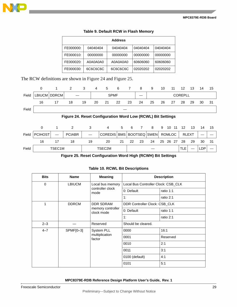
1.8.4 Reset Configuration WordThe reset configuration word (RCW) controls the clock ratios and other basic device functions such as PCI host or agent mode, boot location, TSEC modes, and endian mode. The reset configuration word is divided into reset configuration word lower (RCWL) and reset configuration word higher (RCWH) and is loaded from the local bus during the power-on or hard reset flow. The default RCW low bit setting is 0x0404_0000. The default RCW high bit setting is 0xA060_6C02.
The RCW is located at the lowest 64 bytes of the boot Flash memory, which is 0xFE00_0000 if the default memory map is used.
I2C1-SCL
I2C EEROMM24256
MPC8379E
SCL
SDAI2C1-SDA
I2C Address = 0x50
MPC8379E-RDB Reference Design Platform User’s Guide, Rev. 1
Freescale Semiconductor 29 Preliminary—Subject to Change Without Notice
MPC8379E-RDB Board
The RCW definitions are shown in Figure 24 and Figure 25.
Table 9. Default RCW in Flash Memory
Address
FE000000: 04040404 04040404 04040404 04040404
FE000010: 00000000 00000000 00000000 00000000
FE000020: A0A0A0A0 A0A0A0A0 60606060 60606060
FE000030: 6C6C6C6C 6C6C6C6C 02020202 02020202
0 1 2 3 4 5 6 7 8 9 10 11 12 13 14 15
Field LBIUCM DDRCM — SPMF — COREPLL
16 17 18 19 20 21 22 23 24 25 26 27 28 29 30 31
Field —
Figure 24. Reset Configuration Word Low (RCWL) Bit Settings
0 1 2 3 4 5 6 7 8 9 10 11 12 13 14 15
Field PCIHOST — PCIABR — COREDIS BMS BOOTSEQ SWEN ROMLOC RLEXT — —
16 17 18 19 20 21 22 23 24 25 26 27 28 29 30 31
Field TSEC1M TSEC2M — TLE — LDP —
Figure 25. Reset Configuration Word High (RCWH) Bit Settings
Table 10. RCWL Bit Descriptions
Bits Name Meaning Description
0 LBIUCM Local bus memory controller clock mode
Local Bus Controller Clock: CSB_CLK
0: Default ratio 1:1
1: ratio 2:1
1 DDRCM DDR SDRAM memory controller clock mode
DDR Controller Clock: CSB_CLK
0: Default ratio 1:1
1: ratio 2:1
2–3 — Reserved Should be cleared.
4–7 SPMF[0–3] System PLL multiplication factor
0000 16:1
0001 Reserved
0010 2:1
0011 3:1
0100 (default) 4:1
0101 5:1
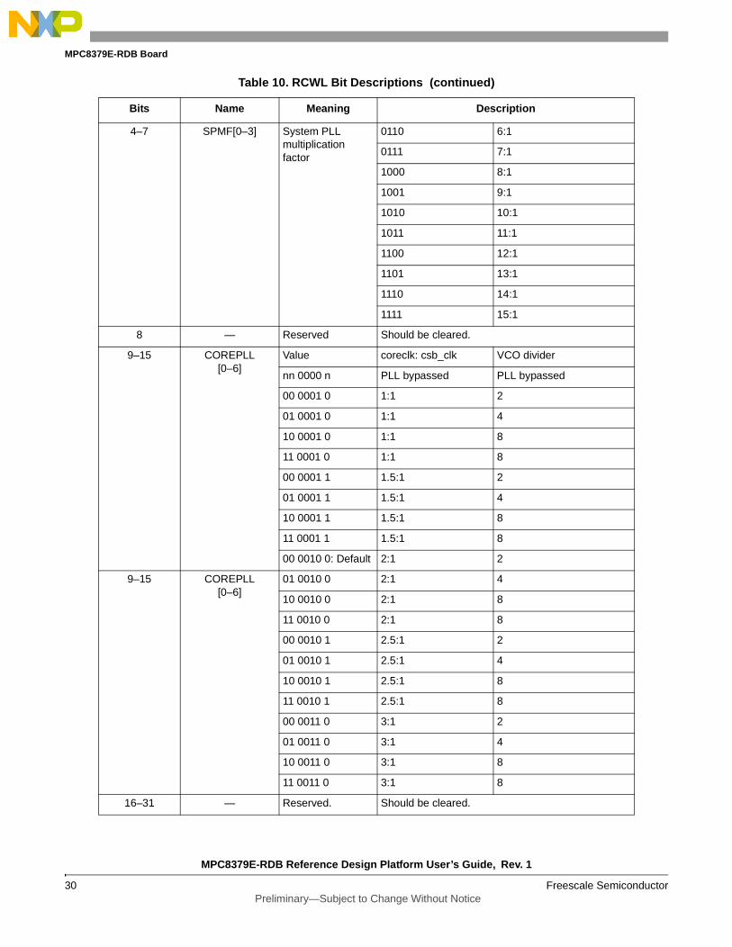
MPC8379E-RDB Reference Design Platform User’s Guide, Rev. 1
30 Freescale Semiconductor Preliminary—Subject to Change Without Notice
MPC8379E-RDB Board
4–7 SPMF[0–3] System PLL multiplication factor
0110 6:1
0111 7:1
1000 8:1
1001 9:1
1010 10:1
1011 11:1
1100 12:1
1101 13:1
1110 14:1
1111 15:1
8 — Reserved Should be cleared.
9–15 COREPLL[0–6]
Value coreclk: csb_clk VCO divider
nn 0000 n PLL bypassed PLL bypassed
00 0001 0 1:1 2
01 0001 0 1:1 4
10 0001 0 1:1 8
11 0001 0 1:1 8
00 0001 1 1.5:1 2
01 0001 1 1.5:1 4
10 0001 1 1.5:1 8
11 0001 1 1.5:1 8
00 0010 0: Default 2:1 2
9–15 COREPLL[0–6]
01 0010 0 2:1 4
10 0010 0 2:1 8
11 0010 0 2:1 8
00 0010 1 2.5:1 2
01 0010 1 2.5:1 4
10 0010 1 2.5:1 8
11 0010 1 2.5:1 8
00 0011 0 3:1 2
01 0011 0 3:1 4
10 0011 0 3:1 8
11 0011 0 3:1 8
16–31 — Reserved. Should be cleared.
Table 10. RCWL Bit Descriptions (continued)
Bits Name Meaning Description

MPC8379E-RDB Reference Design Platform User’s Guide, Rev. 1
Freescale Semiconductor 31 Preliminary—Subject to Change Without Notice
MPC8379E-RDB Board
Table 11. Reset Configuration Word High (RCWH) Bit Descriptions
Bits Name Meaning Detailed Description
0 PCIHOST PCI host mode 0 PCI agent
1: Default PCI host
1 Reserved — Should be cleared
2 PCIARB PCI arbiter 0 PCI arbiter disabled
1: Default PCI arbiter enabled
3 Reserved — Should be cleared
4 COREDIS Core disable mode 0: Default e300 enabled
1 e300 disabled
5 BMS Boot memory space
0: Default 0x0000_0000–0x007F_FFFF
1 0xFF80_0000–0xFFFF_FFFF
6–7 BOOTSEQ Boot sequencer configuration
00: Default Boot sequencer is disabled
01 Boot sequencer load configuration from I2C
10 Boot sequencer load configuration from EEPROM
11 Reserved
8 SWEN Software watchdog enable
0: Default Disabled
1 Enabled
9–11 ROMLOC Boot ROM interface location
000 DDR SDRAM
001 PCI1
010 Reserved
011 On-chip Boot ROM
100 Reserved
101 Local bus GPCM, 8 bits
110: Default Local bus GPCM, 16 bits
111 Local bus GPCM, 32 bits
12–13 RLEXT Boot ROM location extension
00: Default Legacy mode
01 NAND Flash mode
10 Reserved
11 Reserved
14–15 Reserved — Should be cleared
MPC8379E-RDB Reference Design Platform User’s Guide, Rev. 1
32 Freescale Semiconductor Preliminary—Subject to Change Without Notice
MPC8379E-RDB Board
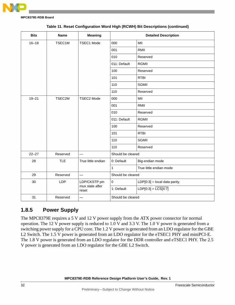
1.8.5 Power SupplyThe MPC8379E requires a 5 V and 12 V power supply from the ATX power connector for normal operation. The 12 V power supply is reduced to 1.0 V and 3.3 V. The 1.0 V power is generated from a switching power supply for a CPU core. The 1.2 V power is generated from an LDO regulator for the GBE L2 Switch. The 1.5 V power is generated from an LDO regulator for the eTSEC1 PHY and miniPCI-E. The 1.8 V power is generated from an LDO regulator for the DDR controller and eTSEC1 PHY. The 2.5 V power is generated from an LDO regulator for the GBE L2 Switch.
16–18 TSEC1M TSEC1 Mode 000 MII
001 RMII
010 Reserved
011: Default RGMII
100 Reserved
101 RTBI
110 SGMII
110 Reserved
19–21 TSEC2M TSEC2 Mode 000 MII
001 RMII
010 Reserved
011: Default RGMII
100 Reserved
101 RTBI
110 SGMII
110 Reserved
22–27 Reserved — Should be cleared
28 TLE True little endian 0: Default Big-endian mode
1 True little endian mode
29 Reserved — Should be cleared
30 LDP LDP/CKSTP pin mux state after reset
0 LDP[0:3] = local data parity.
1: Default LDP[0:3] = LCS[4:7]
31 Reserved — Should be cleared
Table 11. Reset Configuration Word High (RCWH) Bit Descriptions (continued)
Bits Name Meaning Detailed Description
MPC8379E-RDB Reference Design Platform User’s Guide, Rev. 1
Freescale Semiconductor 33 Preliminary—Subject to Change Without Notice
MPC8379E-RDB Board
1.8.6 Chip-Select Assignments and Memory MapTable 12 shows an example memory map on the MPC8379E that is used for u-boot 1.1.3 in the Flash memory.
1.9 SpecificationsTable 13 lists the specifications of the MPC8379E-RDB board.
.
Table 12. Example Memory Map, Local Access Window, and Chip-Select Assignments
Address Range Target InterfaceChip-Select
LineDevice Name Port Size (Bits)
0x0000_0000–0x0FFF_FFFF DDR MCS0 DDR SDRAM (256 Mbyte) 64
0x8000_0000–0x9FFF_FFFF PCI1 Nil PCI1 memory space (512 Mbyte) 32
0xE200_0000–0xE2FF_FFFF PCI1 Nil PCI1 I/O space (16 Mbyte) 32
0xA000_0000–0xBFFF_FFFF PCI2 Nil PCI2 memory space (512 Mbyte) 32
0xE300_0000–0xE3FF_FFFF PCI2 Nil PCI2 I/O space (16 Mbyte) 32
0xF800_0000–0xF801_FFFF Local bus LCS2 GBE L2 Switch VSC7385 8
0xE000_0000–0xEFFF_FFFF Internal bus Nil IMMR (1 Mbyte) —
0x????_0000–0x????_7FFF NAND Controller LCS1# NAND Flash window (32Kbyte) 8
0xFE00_0000–0xFE7F_FFFF Local bus LCS0 NOR Flash memory (8 Mbyte) 16
Table 13. MPC8379E-RDB Board Specifications
Characteristics Specifications
Power requirements: Typical Maximum5.0 V DC TBD TBD12.0 V DC TBD TBD
Communication processor MPC8377E / MPC8379E running @ up to 667MHz
Addressing: Total address range
Flash memory (local bus)DDR SDRAM
4 Gbyte (32 address lines)
8 Mbyte NOR Flash32/64 Mbyte NAND Flash256 Mbyte DDR2 SDRAM at DDR400
Operating temperature 0oC to 70oC (room temperature)
Storage temperature –25oC to 85oC
Relative humidity 5% to 90% (noncondensing)
PCB dimensions:
LengthWidthThickness
6692 mil6692 mil67 mil
MPC8379E-RDB Reference Design Platform User’s Guide, Rev. 1
34 Freescale Semiconductor Preliminary—Subject to Change Without Notice
Getting Started
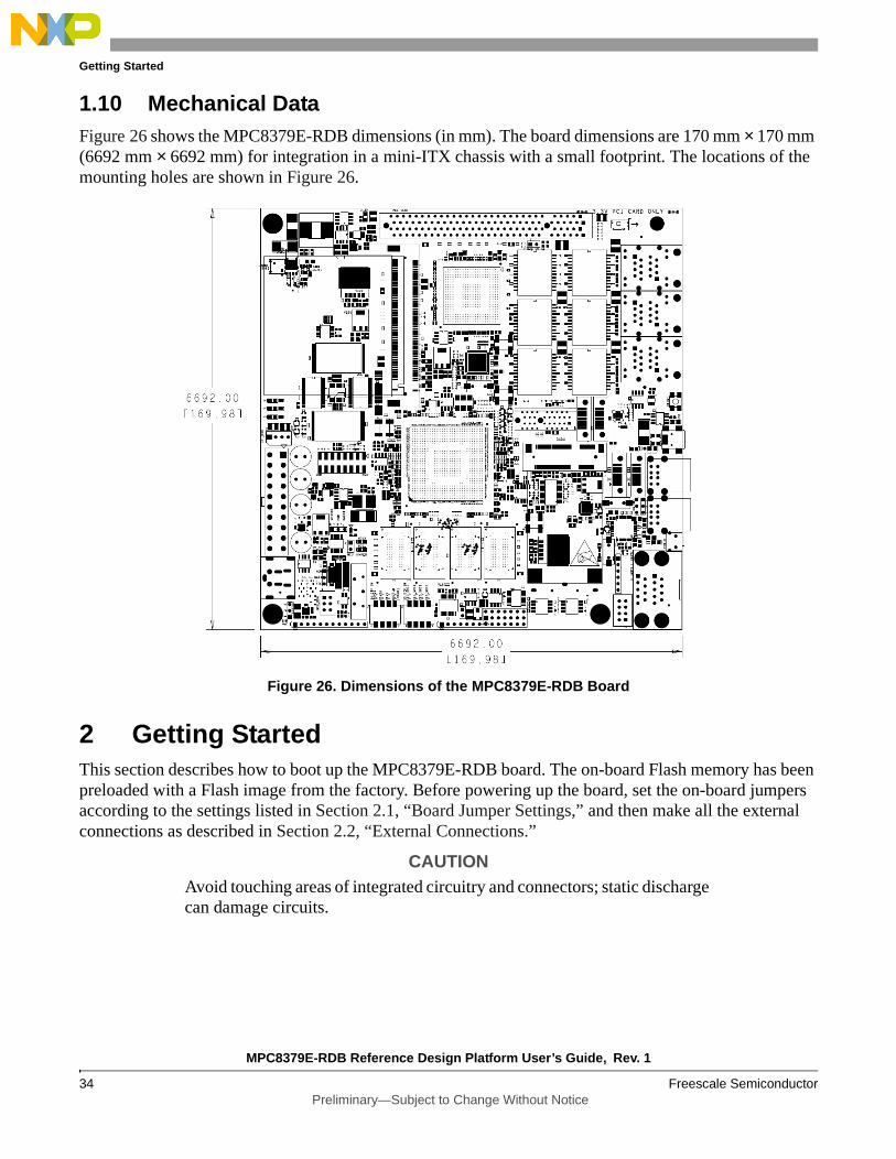
1.10 Mechanical DataFigure 26 shows the MPC8379E-RDB dimensions (in mm). The board dimensions are 170 mm × 170 mm (6692 mm × 6692 mm) for integration in a mini-ITX chassis with a small footprint. The locations of the mounting holes are shown in Figure 26.
Figure 26. Dimensions of the MPC8379E-RDB Board
2 Getting StartedThis section describes how to boot up the MPC8379E-RDB board. The on-board Flash memory has been preloaded with a Flash image from the factory. Before powering up the board, set the on-board jumpers according to the settings listed in Section 2.1, “Board Jumper Settings,” and then make all the external connections as described in Section 2.2, “External Connections.”
CAUTIONAvoid touching areas of integrated circuitry and connectors; static discharge can damage circuits.

MPC8379E-RDB Reference Design Platform User’s Guide, Rev. 1
Freescale Semiconductor 35 Preliminary—Subject to Change Without Notice
Getting Started
2.1 Board Jumper SettingsFigure 27 shows the top view of the MPC8379E-RDB with pin 1 marked for each reference. Using Figure 27 as a guide, the default jumper settings are given in Table 14 starting at the left-hand top corner of the board and moving around the board in a clockwise manner.
Figure 27. MPC8379E-RDB Top View
Pin 1
SA
TA0
RS-232-COM1 (top)
D3
USB
P2
BT1 Battery Holder
D12
P1
USB3 (top)
USB4 (bottom)
USB1 (top)
USB2 (bottom)
ENET1 (top)ENET2 (bottom)
ENET3 (top)ENET4 (bottom)
ENET0 (top)ENET5 (bottom)
Reset
J41
J40
J5
3.3V 32-bits PCI
COP Connector
P22
P23
P21
P20
P19
P8
P15
P7
J8
J42
D15
P16
P6
S1 PowerOn
S2
RS-232-COM2 (bottom)P11
P9
AT
X P
ower
J38
J36
J37
J43
JP2
JP1
J28D14D28
D22
P18
PCI-E (1X)
P18
Mini PCI
P3
SA
TA1
SA
TA2
SA
TA3
mini PCI-E
P14
SD Card (bottom side)
D4D5
S4 S3
CF
G_R
ST
_SR
C0
CF
G_R
ST
_SR
C1
CF
G_R
ST
_SR
C2
CF
G_R
ST
_SR
C3
RS
VD
1R
SV
D0
RE
V1
BO
OT
1# (
NA
ND
)
MPC8379E
P17
P24
D6D7D8D9
1 2 3 4
ON
1 2 3 4
ON
0
1
MPC8379E-RDB Reference Design Platform User’s Guide, Rev. 1
36 Freescale Semiconductor Preliminary—Subject to Change Without Notice
Getting Started
Set the jumpers to their default settings as given in Table 14.
2.2 External ConnectionsDo not turn on power until all cables have been connected and the serial port has been configured as described in Section 2.3, “Serial Port Configuration (PC).”
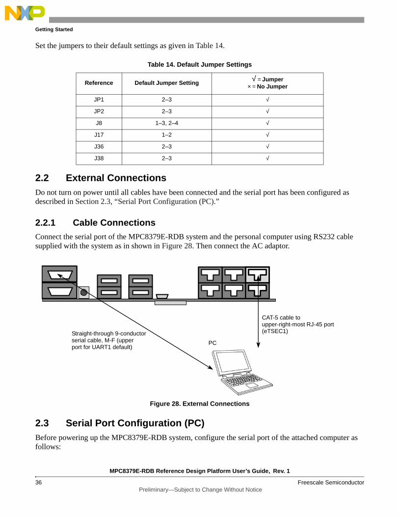
2.2.1 Cable ConnectionsConnect the serial port of the MPC8379E-RDB system and the personal computer using RS232 cable supplied with the system as in shown in Figure 28. Then connect the AC adaptor.
Figure 28. External Connections
2.3 Serial Port Configuration (PC)Before powering up the MPC8379E-RDB system, configure the serial port of the attached computer as follows:
Table 14. Default Jumper Settings
Reference Default Jumper Setting√ = Jumper
× = No Jumper
JP1 2–3 √
JP2 2–3 √
J8 1–3, 2–4 √
J17 1–2 √
J36 2–3 √
J38 2–3 √
PC
CAT-5 cable to upper-right-most RJ-45 port(eTSEC1)Straight-through 9-conductor
serial cable, M-F (upperport for UART1 default)
MPC8379E-RDB Reference Design Platform User’s Guide, Rev. 1
Freescale Semiconductor 37 Preliminary—Subject to Change Without Notice
Getting Started
Data rate: 115.2 Kbps,
Number of data bits: 8,
Parity: none,
Number of Stop bits: 1,
Flow Control: Disabled.
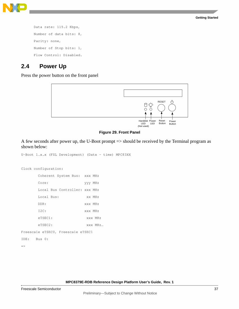
2.4 Power UpPress the power button on the front panel
Figure 29. Front Panel
A few seconds after power up, the U-Boot prompt => should be received by the Terminal program as shown below:
U-Boot 1.x.x (FSL Development) (Date - time) MPC83XX
Clock configuration:
Coherent System Bus: xxx MHz
Core: yyy MHz
Local Bus Controller: xxx MHz
Local Bus: xx MHz
DDR: xxx MHz
I2C: xxx MHz
eTSEC1: xxx MHz
eTSEC2: xxx MHz…
Freescale eTSEC0, Freescale eTSEC1
IDE: Bus 0:
=>
RESET
PowerButton
ResetButton
HarddiskLED
PowerLED
(Not used)
MPC8379E-RDB Reference Design Platform User’s Guide, Rev. 1
38 Freescale Semiconductor Preliminary—Subject to Change Without Notice
Getting Started
NOTEThe normal function of the product may be disturbed by strong electromagnetic interference. If so, simply reset the product to resume normal operation by following the instruction manual. If normal function does not resume, please use the product in another location

MPC8379E-RDB Reference Design Platform User’s Guide, Rev. 1
Freescale Semiconductor 39 Preliminary—Subject to Change Without Notice
MPC8379E-RDB Software
3 MPC8379E-RDB SoftwareA board support package (BSP) is pre-installed on the MPC8379E-RDB. This BSP consists of a bootloader (u-boot), a generic PPC Linux-based system, and associated file system. U-boot and the Linux kernel reside in the on-board Flash memory while the File system is pre-installed on the hard disk shipped with the MPC8379E-RDB. Upon power up, the Linux system is running on the MPC8379E-RDB.
The MPC8379E-RDB BSP generation takes advantage of a tool called the Linux Target Image Builder or LTIB. LTIB is a suite of tools that leverages existing Open Source configuration scripts and source code packages and bundles them all into a single BSP generation bundle. The source code packages include boot loaders and Linux kernel sources as well as many user-space source code packages to build a complete BSP. LTIB also provides compiler packages required to build the BSP. Freescale developers use LTIB to create BSPs for a multitude of Freescale development targets. LTIB leverages as much BSP elements as possible for all Freescale targets that are supported while offering the flexibility required to customize, as necessary, components that require platform specific modifications.
The MPC8379E-RDB BSP release package contains the following:
• MPC8379E-RDB-<yyyymmdd>.iso
This file is an ISO image that may be burned to a CD-ROM or mounted directly from your hard disk. Note that <yyyymmdd> is the release creation date.
The LTIB installation script that installs all necessary packages on a host Linux PC and allows you to modify the BSP and packages within the BSP is in /ltib-MPC8379E-RDB subdirectory within the ISO image.
This ISO image contains a file called Readme.txt which describes all the details required to generate and install the BSP on the MPC8379E-RDB hardware platform. Readme.txt contains the latest information for each BSP release. The ISO image also contains Release Notes.txt which describes changes to the current BSP version versus earlier releases.
To rebuild the BSP package or to add application software, follow the instructions in the Readme.txt very carefully. Readme.txt is part of the ISO release and it contains specific details on how to build, run, and install the BSP. When followed closely the Readme.txt will guide the user to achieve a successful re-installation of the BSP on the MPC8379E-RDB platform.
This ISO image contains the following documents as well:
— MPC8379EMITXUG.pdf, this user's guide document in pdf format
— MPC8379E-RDB_schematic.pdf, the platform schematic in pdf format
— SEC2SWUG.pdf: User's Guide for the Driver software of the Security engine. This document details the driver software interface of the Security Engine to boost the throughput performance of Security applications such as IPSec.
— LtibFaq.pdf, Frequently Asked Questions for LTIB, which is a useful document describing how to make use of LTIB to build the ISO image.
For more information on the MPC8379E-RDB system, please visit Freescale website at http://www.freescale.com.

MPC8379E-RDB Reference Design Platform User’s Guide, Rev. 1
40 Freescale Semiconductor Preliminary—Subject to Change Without Notice
Revision History
3.1 Third-Party Application SoftwareMany third-party applications are available for the MPC8379E-RDB. They are typically built on top of the original BSP delivered by Freescale and they can be installed on the hard disk. To run demonstrations or to acquire details of Freescale’s third-party applications for this MPC8379E-RDB, please contact your local Freescale sales office.
4 Revision History Table 15 provides a revision history for this document.
5 Schematic
Table 15. Document Revision History
Revision Date Substantive Change(s)
0 8/2007 Initial release.

MPC8379E-RDB Reference Design Platform User’s Guide, Rev. 1
Freescale Semiconductor 41 Preliminary—Subject to Change Without Notice
Schematic

MPC8379E-RDB Reference Design Platform User’s Guide, Rev. 1
42 Freescale Semiconductor Preliminary—Subject to Change Without Notice
Schematic

MPC8379E-RDB Reference Design Platform User’s Guide, Rev. 1
Freescale Semiconductor 43 Preliminary—Subject to Change Without Notice
Schematic

MPC8379E-RDB Reference Design Platform User’s Guide, Rev. 1
44 Freescale Semiconductor Preliminary—Subject to Change Without Notice
Schematic

MPC8379E-RDB Reference Design Platform User’s Guide, Rev. 1
Freescale Semiconductor 45 Preliminary—Subject to Change Without Notice
Schematic

MPC8379E-RDB Reference Design Platform User’s Guide, Rev. 1
46 Freescale Semiconductor Preliminary—Subject to Change Without Notice
Schematic

MPC8379E-RDB Reference Design Platform User’s Guide, Rev. 1
Freescale Semiconductor 47 Preliminary—Subject to Change Without Notice
Schematic

MPC8379E-RDB Reference Design Platform User’s Guide, Rev. 1
48 Freescale Semiconductor Preliminary—Subject to Change Without Notice
Schematic

MPC8379E-RDB Reference Design Platform User’s Guide, Rev. 1
Freescale Semiconductor 49 Preliminary—Subject to Change Without Notice
Schematic

MPC8379E-RDB Reference Design Platform User’s Guide, Rev. 1
50 Freescale Semiconductor Preliminary—Subject to Change Without Notice
Schematic

MPC8379E-RDB Reference Design Platform User’s Guide, Rev. 1
Freescale Semiconductor 51 Preliminary—Subject to Change Without Notice
Schematic

MPC8379E-RDB Reference Design Platform User’s Guide, Rev. 1
52 Freescale Semiconductor Preliminary—Subject to Change Without Notice
Schematic

MPC8379E-RDB Reference Design Platform User’s Guide, Rev. 1
Freescale Semiconductor 53 Preliminary—Subject to Change Without Notice
Schematic

MPC8379E-RDB Reference Design Platform User’s Guide, Rev. 1
54 Freescale Semiconductor Preliminary—Subject to Change Without Notice
Schematic

MPC8379E-RDB Reference Design Platform User’s Guide, Rev. 1
Freescale Semiconductor 55 Preliminary—Subject to Change Without Notice
Schematic
Document Number: MPC8379ERDBUGRev. 18/2007
Preliminary—Subject to Change Without Notice
Freescale™ and the Freescale logo are trademarks of Freescale Semiconductor, Inc. The Power Architecture and Power.org word marks and the Power and Power.org logos and related marks are trademarks and service marks licensed by Power.org. All other product or service names are the property of their respective owners.
© Freescale Semiconductor, Inc., 2007.
Information in this document is provided solely to enable system and software
implementers to use Freescale Semiconductor products. There are no express or
implied copyright licenses granted hereunder to design or fabricate any integrated
circuits or integrated circuits based on the information in this document.
Freescale Semiconductor reserves the right to make changes without further notice to
any products herein. Freescale Semiconductor makes no warranty, representation or
guarantee regarding the suitability of its products for any particular purpose, nor does
Freescale Semiconductor assume any liability arising out of the application or use of
any product or circuit, and specifically disclaims any and all liability, including without
limitation consequential or incidental damages. “Typical” parameters which may be
provided in Freescale Semiconductor data sheets and/or specifications can and do
vary in different applications and actual performance may vary over time. All operating
parameters, including “Typicals” must be validated for each customer application by
customer’s technical experts. Freescale Semiconductor does not convey any license
under its patent rights nor the rights of others. Freescale Semiconductor products are
not designed, intended, or authorized for use as components in systems intended for
surgical implant into the body, or other applications intended to support or sustain life,
or for any other application in which the failure of the Freescale Semiconductor product
could create a situation where personal injury or death may occur. Should Buyer
purchase or use Freescale Semiconductor products for any such unintended or
unauthorized application, Buyer shall indemnify and hold Freescale Semiconductor
and its officers, employees, subsidiaries, affiliates, and distributors harmless against all
claims, costs, damages, and expenses, and reasonable attorney fees arising out of,
directly or indirectly, any claim of personal injury or death associated with such
unintended or unauthorized use, even if such claim alleges that Freescale
Semiconductor was negligent regarding the design or manufacture of the part.
How to Reach Us:
Home Page: www.freescale.com
email: [email protected]
USA/Europe or Locations Not Listed: Freescale Semiconductor Technical Information Center, CH3701300 N. Alma School Road Chandler, Arizona 85224 [email protected]
Europe, Middle East, and Africa:Freescale Halbleiter Deutschland GmbHTechnical Information CenterSchatzbogen 781829 Muenchen, Germany+44 1296 380 456 (English) +46 8 52200080 (English)+49 89 92103 559 (German)+33 1 69 35 48 48 (French) [email protected]
Japan: Freescale Semiconductor Japan Ltd. HeadquartersARCO Tower 15F1-8-1, Shimo-Meguro, Meguro-ku Tokyo 153-0064, Japan 0120 191014+81 3 5437 [email protected]
Asia/Pacific: Freescale Semiconductor Hong Kong Ltd. Technical Information Center2 Dai King Street Tai Po Industrial Estate, Tai Po, N.T., Hong Kong +800 2666 [email protected]
For Literature Requests Only:Freescale Semiconductor
Literature Distribution Center P.O. Box 5405Denver, Colorado 80217 1-800-441-2447303-675-2140Fax: 303-675-2150LDCForFreescaleSemiconductor
@hibbertgroup.com