Embed Size (px)
Citation preview

1. Product profile
1.1 General descriptionThe KMA199E is a magnetic angle sensor system. The MagnetoResistive (MR) sensorbridges and the mixed signal Integrated Circuit (IC) are integrated into a single package.
This angular measurement system KMA199E is pre-programmed, pre-calibrated andtherefore, ready to use.
The KMA199E allows user specific adjustments of angular range, zero angle andclamping voltages. The settings are stored permanently in an Electrically ErasableProgrammable Read-Only Memory (EEPROM).
1.2 Features
KMA199EProgrammable angle sensorRev. 01 — 18 October 2007 Product data sheet
n High precision sensor for magneticangular measurement
n Ratiometric output voltage
n Programmable user adjustments,including zero angle and angular range
n Independent from the magnetic fieldstrength above 35 kA/m
n Single package sensor system n Programming via One-Wire Interface(OWI)
n Magnet-lost and power-lost detection n Fail-safe EEPROMn Built-in transient protection n High temperature rangen User-programmable 32-bit identifier n Factory calibratedn Ready to use
NXP Semiconductors KMA199EProgrammable angle sensor
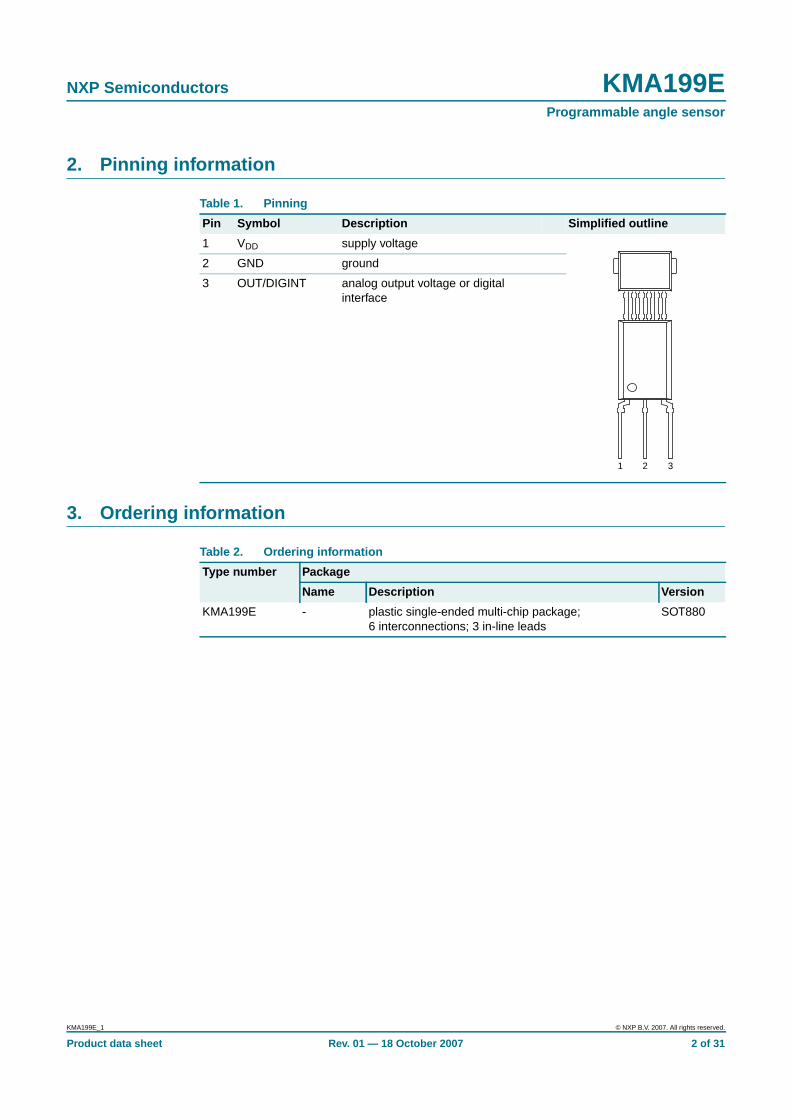
2. Pinning information
3. Ordering information
Table 1. Pinning
Pin Symbol Description Simplified outline
1 VDD supply voltage
2 GND ground
3 OUT/DIGINT analog output voltage or digitalinterface
1 2 3
Table 2. Ordering information
Type number Package
Name Description Version
KMA199E - plastic single-ended multi-chip package;6 interconnections; 3 in-line leads
SOT880
KMA199E_1 © NXP B.V. 2007. All rights reserved.
Product data sheet Rev. 01 — 18 October 2007 2 of 31
xxxx xxxxxxxxxxxxxxxxxxxxxxxxxxxxxx x xxxxxxxxxxxxxx xxxxxxxxxx xxx xxxxxx xxxxxxxxxxxxxxxxxxxxxxx xxxxxxxxxxxxxxxxxxxxxxxxxxx xxxxxx xx xxxxxxxxxxxxxxxxxxxxxxxxxxxxx xxxxxxxxxxxxxxxxxxxxxx xxxxxxxxxxx xxxxxxx xxxxxxxxxxxxxxxxxxxxxxxxxxxxxxxxxxx xxxxxxxxxxxxxx xxxxxx xx xxxxxxxxxxxxxxxxxxxxxxxxxxxxxxxx xxxxxxxxxxxxxxxxxxxxxxxx xxxxxxxxxxxxxxxxxxxxxxxxxxxxxxxxxxxxxxxxxxxxxxxxxxxxx xxxxxxxxxxx xxxxx x x
KM
A199E
_1
Product data shee
NX
P S
emiconducto
4.F
unctional di
t
rsK
MA
199EP
rogramm
able angle sensor
agram
001aag809
internalprotection
diodes
POWERLOST
POWERLOST
VSSE
VDDE
VO OUT/DIGINT
VDD
GND
CL
Cblock
© N
XP
B.V. 2007. A
ll rights reserved.
Rev. 01 —
18 October 2007
3 of 31
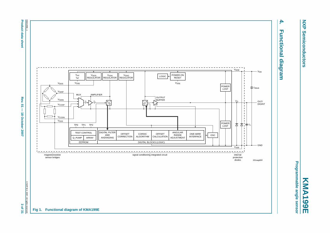
Fig 1. Functional diagram of KMA199E
2 2
signal conditioning integrated circuitmagnetoresistivesensor bridges
TP0
VSINP
MUX
AD
AMPLIFIER
VSSEVDDS
VSINN
VCOSP
VCOSN
VSSS
A
OUTPUTBUFFER
D
VDDSREGULATOR
VDDAREGULATOR
DIGITAL FILTERAND
AVERAGING
CORDICALGORITHM
DIGITAL BLOCKS (LOGIC)
OFFSETCALCULATION
OFFSETCORRECTION
ONE-WIREINTERFACE
ANGULARRANGE
ADJUSTMENT
VDDDREGULATOR
VrefIref
POWER-ONRESET
LOGIC
Q_PUMP ARRAY
TEST CONTROL
EEPROM
OSC
TP1 TP2
VSSE
NXP Semiconductors KMA199EProgrammable angle sensor
5. Functional description
The KMA199E amplifies two orthogonal differential signals, which are delivered by MRsensor bridges and converts them into the digital domain. The angle is calculated usingthe COordinate Rotation DIgital Computer (CORDIC) algorithm. After a digital-to-analogconversion the analog signal is provided to the output. Thus, the output is a linearrepresentation of the angular value. Zero angle, clamping voltages and angular range areprogrammable. In addition, two 16-bit registers are available for customer purposes, likesample identification.
The KMA199E comprises a Cyclic Redundancy Check (CRC) and an Error Detection andCorrection (EDC) supervision, as well as a magnet-lost detection to ensure a fail-safeoperation. A power-lost detection circuit pulls the analog output to the remaining supplyline, if either the supply voltage or the ground line is interrupted.
After multiplexing the two MR Wheatstone bridge signals and their successiveamplification, the signal is converted into the digital domain by an Analog-to-DigitalConverter (ADC). Further processing is done within an on-chip state machine. Thisincludes offset cancellation, calculation of the mechanical angle using the CORDICalgorithm, as well as zero angle and angular range adjustment. The internalDigital-to-Analog Converter (DAC) and the analog output stage are used for conversion ofthe angle information into an analog output voltage, which is ratiometric to the supplyvoltage.
The configuration parameters are stored in an user-programmable EEPROM. For thispurpose the OWI, which is accessible via the pin OUT/DIGINT, is used.
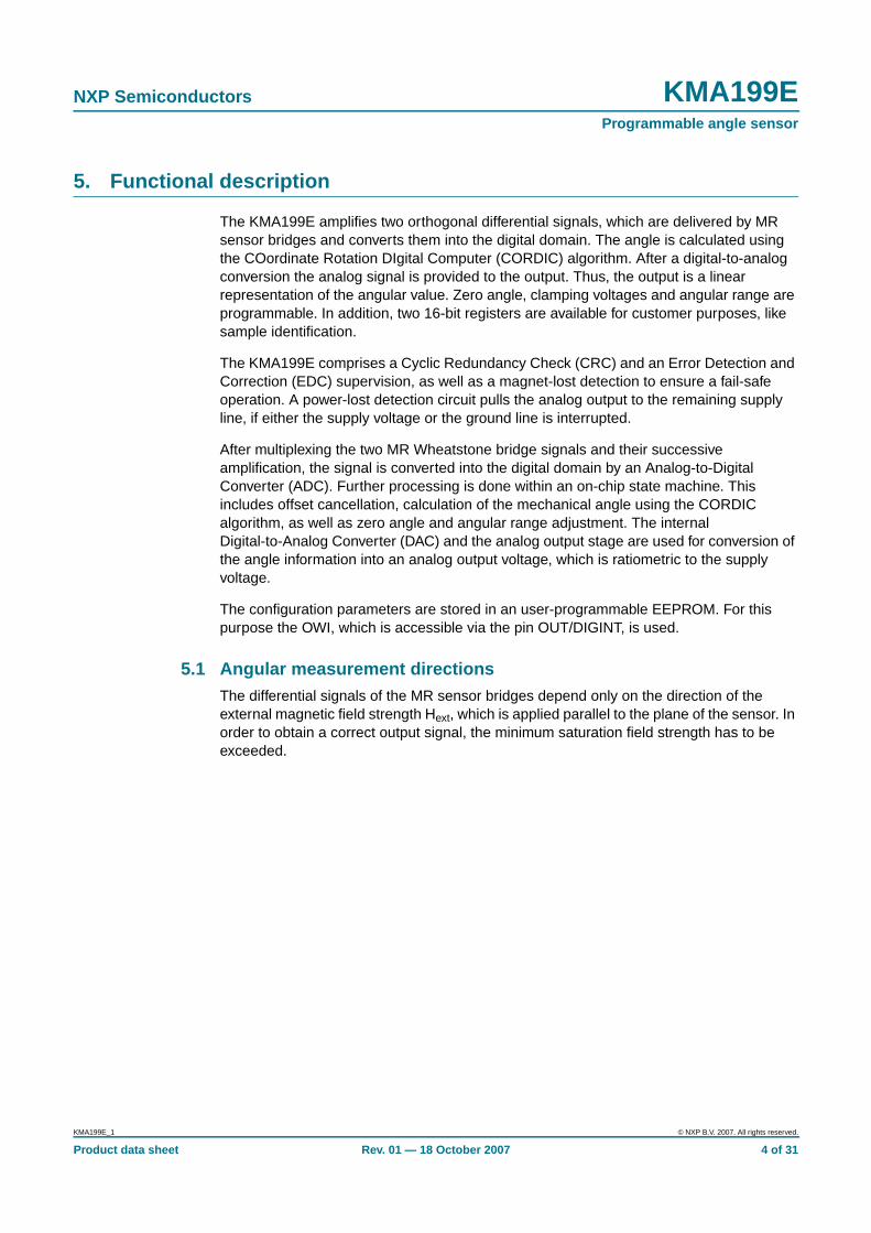
5.1 Angular measurement directionsThe differential signals of the MR sensor bridges depend only on the direction of theexternal magnetic field strength Hext, which is applied parallel to the plane of the sensor. Inorder to obtain a correct output signal, the minimum saturation field strength has to beexceeded.
KMA199E_1 © NXP B.V. 2007. All rights reserved.
Product data sheet Rev. 01 — 18 October 2007 4 of 31
NXP Semiconductors KMA199EProgrammable angle sensor
Since the Anisotropic MR (AMR) effect is periodic over 180°, the sensor output is also180°-periodic, whereas the angle is calculated relative to a freely programmable zeroangle. The dashed line indicates the mechanical zero degree position.
6. Diagnostic features
The KMA199E provides four diagnostic features:
6.1 EEPROM CRC and EDC supervisionThe KMA199E includes a supervision of the programmed data. At power-on, a CRC of theEEPROM is done. Furthermore the EEPROM is protected against bit errors. For thispurpose every 16-bit data word is saved internally as a 22-bit word. The protection logiccorrects any single-bit error in a data word, while the sensor continues in normal operationmode and can detect all double-bit errors by going into diagnostic mode.
6.2 Magnet-lost detectionIf the applied magnetic field strength is not sufficient, the KMA199E raises a diagnosticcondition. In order to enter the diagnostic mode, due to EEPROM CRC or magnet-lostdetection, the device can be programmed for an active diagnostic mode, where the outputis driven below 4 %VDD or above 96 %VDD.
Fig 2. Angular measurement directions
001aag741
Hext
α
KMA199E_1 © NXP B.V. 2007. All rights reserved.
Product data sheet Rev. 01 — 18 October 2007 5 of 31
NXP Semiconductors KMA199EProgrammable angle sensor
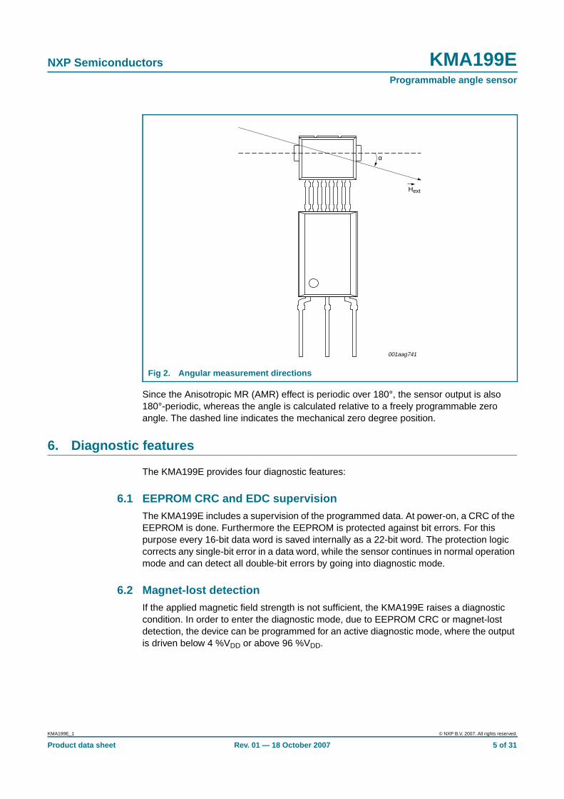
6.3 Power-lost detectionThe power-lost detection circuits enable the detection of an interrupted supply or groundline of the KMA199E. In case of a power-lost condition, two internal switches within thesensor are closed, connecting the pin of the analog output with the pins of the supplyvoltage and the ground.
Table 3 shows the resulting output voltage depending on the error case and the loadresistance.
6.4 Low supply voltage detectionIf the supply voltage is below the switch-off threshold voltage, a status bit is set.
Following table describes the behavior of the analog output at different supply voltages.
Fig 3. Equivalent output circuit in case of a power-lost condition
Table 3. Power-lost behavior
Load resistance Supply voltage lost Ground lost
RL > 5 kΩ VO ≤ 4 %VDD VO ≥ 96 %VDD
001aag810
ZO(pl)
ZO(pl)
OUT/DIGINT
GND
VDDKMA199E
Table 4. Supply voltage behavior
Voltage range Description Analog output
0 V to ≈ 1.5 V the output drives an active LOW, but theswitches of the power-lost detection circuitsare not fully opened and set the output to alevel between ground and half the supplyvoltage
actively driven output to avoltage level between groundand half the supply voltage
≈ 1.5 V to VPOR all modules begin to work and the power-onreset is active
diagnostics at LOW level
VPOR to Vth(on) orVth(off)
all modules begin to work and the digital partis initialized
EEPROM defined diagnosticlevel
Vth(on) or Vth(off) to4.5 V
analog output is switched on after power-ontime and represents the measured angle
analog output of themeasured angle without thespecified accuracy
4.5 V to 5.5 V normal operation where the sensor works withthe specified accuracy
analog output of themeasured angle
KMA199E_1 © NXP B.V. 2007. All rights reserved.
Product data sheet Rev. 01 — 18 October 2007 6 of 31
NXP Semiconductors KMA199EProgrammable angle sensor
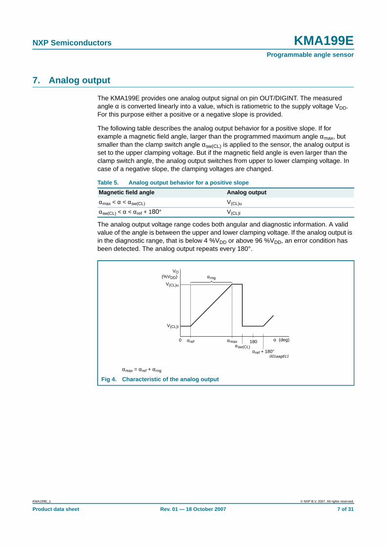
7. Analog output
The KMA199E provides one analog output signal on pin OUT/DIGINT. The measuredangle α is converted linearly into a value, which is ratiometric to the supply voltage VDD.For this purpose either a positive or a negative slope is provided.
The following table describes the analog output behavior for a positive slope. If forexample a magnetic field angle, larger than the programmed maximum angle αmax, butsmaller than the clamp switch angle αsw(CL) is applied to the sensor, the analog output isset to the upper clamping voltage. But if the magnetic field angle is even larger than theclamp switch angle, the analog output switches from upper to lower clamping voltage. Incase of a negative slope, the clamping voltages are changed.
The analog output voltage range codes both angular and diagnostic information. A validvalue of the angle is between the upper and lower clamping voltage. If the analog output isin the diagnostic range, that is below 4 %VDD or above 96 %VDD, an error condition hasbeen detected. The analog output repeats every 180°.
Table 5. Analog output behavior for a positive slope
Magnetic field angle Analog output
αmax < α < αsw(CL) V(CL)u
αsw(CL) < α < αref + 180° V(CL)l
αmax = αref + αrng
Fig 4. Characteristic of the analog output
001aag811
αrng
0 αref αmaxαsw(CL)
αref + 180°
α (deg)180
VO(%VDD)
V(CL)u
V(CL)I
KMA199E_1 © NXP B.V. 2007. All rights reserved.
Product data sheet Rev. 01 — 18 October 2007 7 of 31
NXP Semiconductors KMA199EProgrammable angle sensor
8. Limiting values
[1] Time until sensor environment is initialized.
[2] The maximum value of the output voltage is 5.7 V.
9. Recommended operating conditions
[1] Normal operation mode.
[2] Between ground and analog output, as close as possible to the package.
[3] Between ground and supply voltage, as close as possible to the package and with a low equivalent seriesresistance.
[4] Power-lost detection is only possible with a load resistance within the specified range.
10. Thermal characteristics
Table 6. Limiting valuesIn accordance with the Absolute Maximum Rating System (IEC 60134).
Symbol Parameter Conditions Min Max Unit
VDD supply voltage −0.3 +5.7 V
tinit < 200 h [1] - 6.0 V
VO output voltage [2] −0.3 VDD + 0.3 V
Ir reverse current Tamb < 70 °C - 150 mA
Tamb ambient temperature −40 +160 °C
Tamb(pr) programming ambienttemperature
10 70 °C
Tstg storage temperature −40 +125 °C
EEPROM
tret(D) data retention time Tamb = 50 °C 17 - year
Nendu(W_ER) write or erase endurance Tamb(pr) = 70 °C 100 - cycle
Table 7. Operating conditionsIn a homogenous magnetic field.
Symbol Parameter Conditions Min Typ Max Unit
VDD supply voltage [1] 4.5 5.0 5.5 V
Tamb ambient temperature −40 - +160 °C
Tamb(pr) programming ambient temperature 10 - 70 °C
CL load capacitance [2] 0.33 - 22 nF
Cblock blocking capacitance [3] 75 100 - nF
RL load resistance [4] 5 - ∞ kΩ
Hext external magnetic field strength 35 - - kA/m
Table 8. Thermal characteristics
Symbol Parameter Conditions Typ Unit
Rth(j-a) thermal resistance from junctionto ambient
120 K/W
KMA199E_1 © NXP B.V. 2007. All rights reserved.
Product data sheet Rev. 01 — 18 October 2007 8 of 31
NXP Semiconductors KMA199EProgrammable angle sensor
11. Characteristics
[1] Normal operation mode.
[2] Without load current at the analog output.
Table 9. Supply currentCharacteristics are valid for the operating conditions, as specified in Section 9.
Symbol Parameter Conditions Min Typ Max Unit
IDD supply current [1][2] - - 10 mA
Table 10. Power-on resetCharacteristics are valid for the operating conditions, as specified in Section 9.
Symbol Parameter Conditions Min Typ Max Unit
Vth(on) switch-on thresholdvoltage
analog output switches on, ifVDD > Vth(on)
4.20 4.30 4.49 V
Vth(off) switch-off thresholdvoltage
analog output switches off, ifVDD < Vth(off)
- 4.20 4.30 V
Vhys hysteresis voltage Vhys = Vth(on) − Vth(off) 0.1 - 0.4 V
VPOR power-on reset voltage IC is initialized 2.4 - 3.3 V
Table 11. System performanceCharacteristics are valid for the operating conditions, as specified in Section 9.
Symbol Parameter Conditions Min Typ Max Unit
αres angle resolution [1] - - 0.04 deg
αmax maximum angle programmable angular rangefor V(CL)u − V(CL)l ≥ 80 %VDD
[2] 5 - 180 deg
αref reference angle programmable zero angle [2] 0 - 180 deg
VO(nom) nominal output voltage at full supply operating range 5 - 95 %VDD
VO(udr) upper diagnostic rangeoutput voltage
[3] 96 - 100 %VDD
VO(ldr) lower diagnostic rangeoutput voltage
[3] 0 - 4 %VDD
V(CL)u upper clamping voltage [4] 40 - 95 %VDD
V(CL)l lower clamping voltage [4] 5 - 30.5 %VDD
∆V(CL) clamping voltage variation deviation from programmedvalue
−0.3 - +0.3 %VDD
IO output current normal operation mode;operating as sink or source
- - 2 mA
Vn(o)(RMS) RMS output noise voltage equivalent power noise [5] - 0.4 2.5 mV
∆φlin linearity error [5][6] −1.55 - +1.55 deg
∆φtemp temperature drift error [1][5][6]
[7][8]- - 0.8 deg
∆φtempRT temperature drift error atroom temperature
[6][7][8] - - 0.55 deg
KMA199E_1 © NXP B.V. 2007. All rights reserved.
Product data sheet Rev. 01 — 18 October 2007 9 of 31
NXP Semiconductors KMA199EProgrammable angle sensor
[1] At a nominal output voltage between 5 %VDD and 95 %VDD and a maximum angle of αmax = 180°.
[2] In steps of resolution < 0.022°.
[3] Activation is dependent on the programmed diagnostic mode.
[4] In steps of 0.02 %VDD.
[5] At a low-pass filtered analog output with a cut-off frequency of 0.7 kHz.
[6] See Section 12.
[7] Temperature range −40 °C to +140 °C.
[8] Based on a 3σ standard deviation.
∆φhys hysteresis error referred to input [5][6] - - 0.09 deg
∆φµlin microlinearity error referred to input [5][6] −0.1 - +0.1 deg
ZO(pl) power-lost outputimpedance
impedance to remaining supplyline in case of lost supplyvoltage or lost ground
- - 210 Ω
Table 11. System performance …continuedCharacteristics are valid for the operating conditions, as specified in Section 9.
Symbol Parameter Conditions Min Typ Max Unit
Table 12. DynamicsCharacteristics are valid for the operating conditions, as specified in Section 9.
Symbol Parameter Conditions Min Typ Max Unit
ton turn-on time until first valid result - - 5 ms
fupd update frequency 2 3.125 - kHz
ts settling time after an ideal mechanical anglestep of 45°, until 90 % of thefinal value is reached;CL = 5 nF
- - 1.8 ms
tcmd(ent) enter command mode time after power on 16 - 26 ms
Table 13. Digital interfaceCharacteristics are valid for the operating conditions, as specified in Section 9.
Symbol Parameter Conditions Min Typ Max Unit
VIH HIGH-level input voltage 80 - - %VDD
VIL LOW-level input voltage - - 20 %VDD
VOH HIGH-level output voltage IO = 2 mA 80 - - %VDD
VOL LOW-level output voltage IO = 2 mA - - 20 %VDD
Iod overdrive current absolute value for overdrivingthe output buffer
- - 20 mA
tstart start time LOW level before rising edge 5 - - µs
tstop stop time HIGH level before falling edge 5 - - µs
Tbit bit period minimum period may be limitedby the load capacitance
10 - 100 µs
tw0 pulse width 0 0.175Tbit 0.25Tbit 0.375Tbit s
tw1 pulse width 1 0.625Tbit 0.75Tbit 0.825Tbit s
tto time-out time digital communication resetguaranteed after maximum tto
- - 220 µs
KMA199E_1 © NXP B.V. 2007. All rights reserved.
Product data sheet Rev. 01 — 18 October 2007 10 of 31
NXP Semiconductors KMA199EProgrammable angle sensor
12. Definition of errors
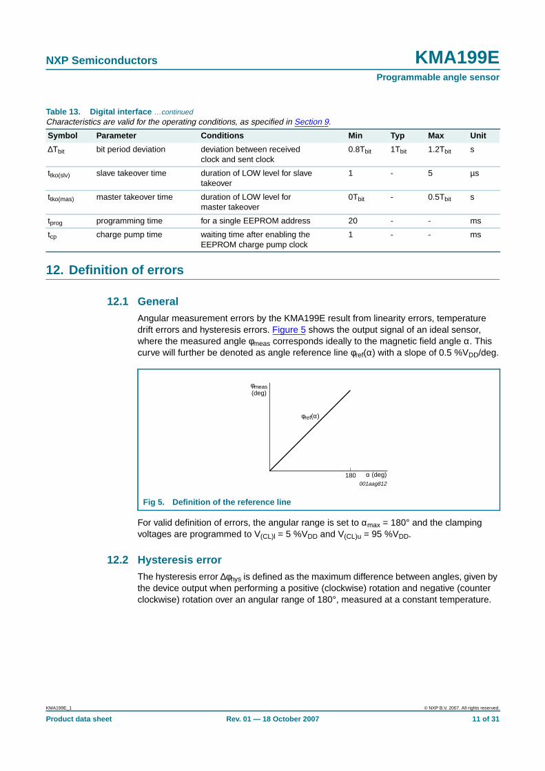
12.1 GeneralAngular measurement errors by the KMA199E result from linearity errors, temperaturedrift errors and hysteresis errors. Figure 5 shows the output signal of an ideal sensor,where the measured angle φmeas corresponds ideally to the magnetic field angle α. Thiscurve will further be denoted as angle reference line φref(α) with a slope of 0.5 %VDD/deg.
For valid definition of errors, the angular range is set to αmax = 180° and the clampingvoltages are programmed to V(CL)l = 5 %VDD and V(CL)u = 95 %VDD.
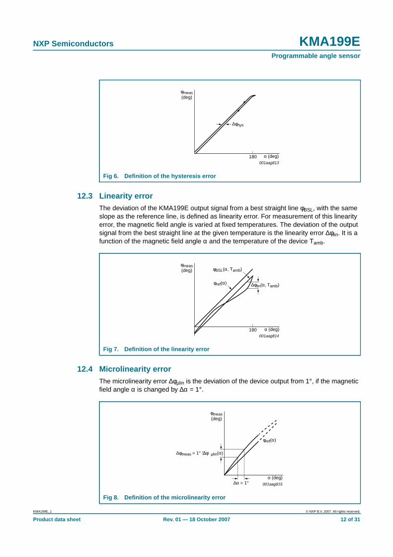
12.2 Hysteresis errorThe hysteresis error ∆φhys is defined as the maximum difference between angles, given bythe device output when performing a positive (clockwise) rotation and negative (counterclockwise) rotation over an angular range of 180°, measured at a constant temperature.
∆Tbit bit period deviation deviation between receivedclock and sent clock
0.8Tbit 1Tbit 1.2Tbit s
ttko(slv) slave takeover time duration of LOW level for slavetakeover
1 - 5 µs
ttko(mas) master takeover time duration of LOW level formaster takeover
0Tbit - 0.5Tbit s
tprog programming time for a single EEPROM address 20 - - ms
tcp charge pump time waiting time after enabling theEEPROM charge pump clock
1 - - ms
Table 13. Digital interface …continuedCharacteristics are valid for the operating conditions, as specified in Section 9.
Symbol Parameter Conditions Min Typ Max Unit
Fig 5. Definition of the reference line
001aag812180 α (deg)
φmeas(deg)
φref(α)
KMA199E_1 © NXP B.V. 2007. All rights reserved.
Product data sheet Rev. 01 — 18 October 2007 11 of 31
NXP Semiconductors KMA199EProgrammable angle sensor
12.3 Linearity errorThe deviation of the KMA199E output signal from a best straight line φBSL, with the sameslope as the reference line, is defined as linearity error. For measurement of this linearityerror, the magnetic field angle is varied at fixed temperatures. The deviation of the outputsignal from the best straight line at the given temperature is the linearity error ∆φlin. It is afunction of the magnetic field angle α and the temperature of the device Tamb.
12.4 Microlinearity errorThe microlinearity error ∆φµlin is the deviation of the device output from 1°, if the magneticfield angle α is changed by ∆α = 1°.
Fig 6. Definition of the hysteresis error
001aag813180 α (deg)
φmeas(deg)
∆φhys
Fig 7. Definition of the linearity error
001aag814180 α (deg)
φmeas(deg)
∆φlin(α, Tamb)φref(α)
φBSL(α, Tamb)
Fig 8. Definition of the microlinearity error
001aag815
α (deg)
φmeas(deg)
∆φmeas = 1° + ∆φµlin(α)
φref(α)
∆α = 1°
KMA199E_1 © NXP B.V. 2007. All rights reserved.
Product data sheet Rev. 01 — 18 October 2007 12 of 31
NXP Semiconductors KMA199EProgrammable angle sensor
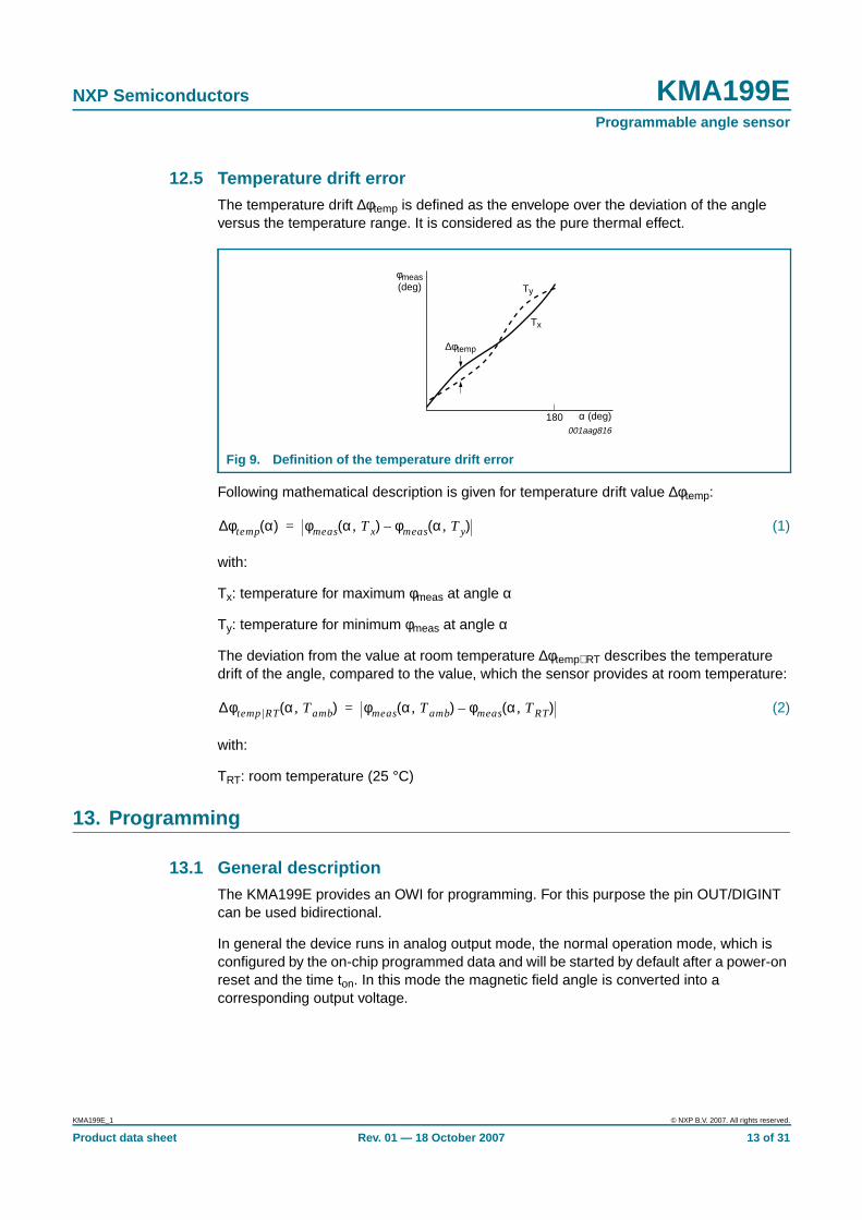
12.5 Temperature drift errorThe temperature drift ∆φtemp is defined as the envelope over the deviation of the angleversus the temperature range. It is considered as the pure thermal effect.
Following mathematical description is given for temperature drift value ∆φtemp:
(1)
with:
Tx: temperature for maximum φmeas at angle α
Ty: temperature for minimum φmeas at angle α
The deviation from the value at room temperature ∆φtempRT describes the temperaturedrift of the angle, compared to the value, which the sensor provides at room temperature:
(2)
with:
TRT: room temperature (25 °C)
13. Programming
13.1 General descriptionThe KMA199E provides an OWI for programming. For this purpose the pin OUT/DIGINTcan be used bidirectional.
In general the device runs in analog output mode, the normal operation mode, which isconfigured by the on-chip programmed data and will be started by default after a power-onreset and the time ton. In this mode the magnetic field angle is converted into acorresponding output voltage.
Fig 9. Definition of the temperature drift error
001aag816180 α (deg)
φmeas(deg)
∆φtemp
Ty
Tx
φtemp∆ α( ) φmeasα Tx,( ) φmeasα Ty,( )–=
∆φtemp RTα Tamb,( ) φmeasα Tamb,( ) φmeasα TRT,( )–=
KMA199E_1 © NXP B.V. 2007. All rights reserved.
Product data sheet Rev. 01 — 18 October 2007 13 of 31
NXP Semiconductors KMA199EProgrammable angle sensor
For programming the command mode has to be entered. In this mode the customer canadjust all required parameters (like zero angle and angular range for example) to his ownapplication. The data can be stored in the EEPROM, after enabling the internal chargepump and waiting for tcp. After changing EEPROM constants, the checksum has to berecalculated and written (see Section 13.4).
In order to enter the command mode, a specific command sequence has to be sent after apower-on reset and during the time slot tcmd(ent). For this purpose the external source,which is used to send the command sequence, has to overdrive the output buffer of theKMA199E, hence it has to provide the current Iod.
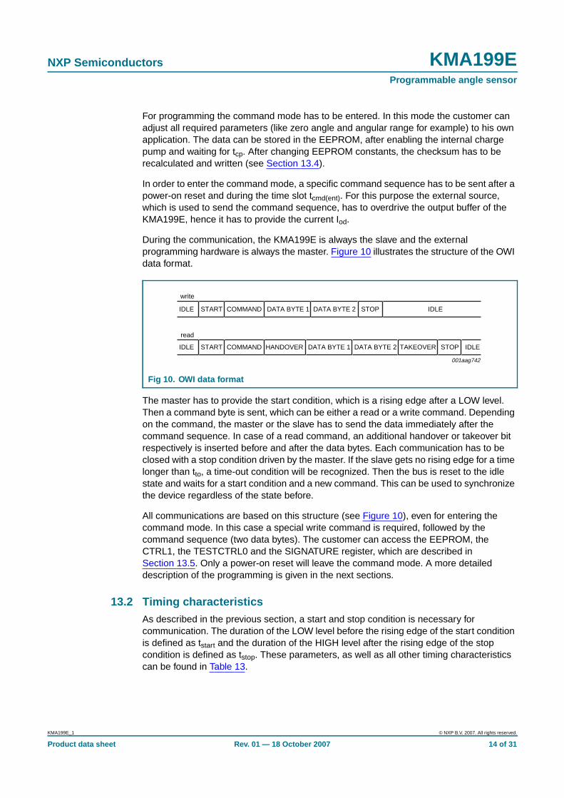
During the communication, the KMA199E is always the slave and the externalprogramming hardware is always the master. Figure 10 illustrates the structure of the OWIdata format.
The master has to provide the start condition, which is a rising edge after a LOW level.Then a command byte is sent, which can be either a read or a write command. Dependingon the command, the master or the slave has to send the data immediately after thecommand sequence. In case of a read command, an additional handover or takeover bitrespectively is inserted before and after the data bytes. Each communication has to beclosed with a stop condition driven by the master. If the slave gets no rising edge for a timelonger than tto, a time-out condition will be recognized. Then the bus is reset to the idlestate and waits for a start condition and a new command. This can be used to synchronizethe device regardless of the state before.
All communications are based on this structure (see Figure 10), even for entering thecommand mode. In this case a special write command is required, followed by thecommand sequence (two data bytes). The customer can access the EEPROM, theCTRL1, the TESTCTRL0 and the SIGNATURE register, which are described inSection 13.5. Only a power-on reset will leave the command mode. A more detaileddescription of the programming is given in the next sections.
13.2 Timing characteristicsAs described in the previous section, a start and stop condition is necessary forcommunication. The duration of the LOW level before the rising edge of the start conditionis defined as tstart and the duration of the HIGH level after the rising edge of the stopcondition is defined as tstop. These parameters, as well as all other timing characteristicscan be found in Table 13.
Fig 10. OWI data format
001aag742
write
IDLE IDLESTART STOPCOMMAND DATA BYTE 1 DATA BYTE 2
IDLE START COMMAND HANDOVER TAKEOVER STOP IDLEDATA BYTE 1 DATA BYTE 2
read
KMA199E_1 © NXP B.V. 2007. All rights reserved.
Product data sheet Rev. 01 — 18 October 2007 14 of 31
NXP Semiconductors KMA199EProgrammable angle sensor
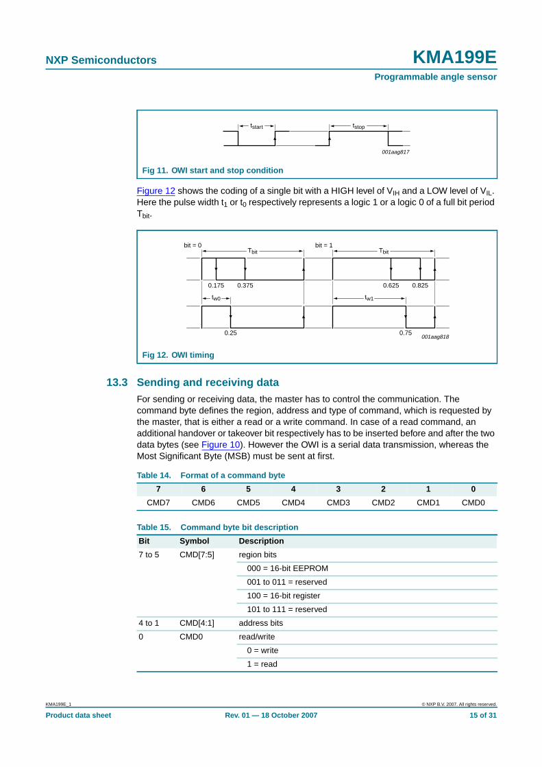
Figure 12 shows the coding of a single bit with a HIGH level of VIH and a LOW level of VIL.Here the pulse width t1 or t0 respectively represents a logic 1 or a logic 0 of a full bit periodTbit.
13.3 Sending and receiving dataFor sending or receiving data, the master has to control the communication. Thecommand byte defines the region, address and type of command, which is requested bythe master, that is either a read or a write command. In case of a read command, anadditional handover or takeover bit respectively has to be inserted before and after the twodata bytes (see Figure 10). However the OWI is a serial data transmission, whereas theMost Significant Byte (MSB) must be sent at first.
Fig 11. OWI start and stop condition
Fig 12. OWI timing
001aag817
tstart tstop
001aag818
0.175
bit = 0 bit = 1
0.25
0.375
Tbit
tw0 tw1
0.625
0.75
0.825
Tbit
Table 14. Format of a command byte
7 6 5 4 3 2 1 0
CMD7 CMD6 CMD5 CMD4 CMD3 CMD2 CMD1 CMD0
Table 15. Command byte bit description
Bit Symbol Description
7 to 5 CMD[7:5] region bits
000 = 16-bit EEPROM
001 to 011 = reserved
100 = 16-bit register
101 to 111 = reserved
4 to 1 CMD[4:1] address bits
0 CMD0 read/write
0 = write
1 = read
KMA199E_1 © NXP B.V. 2007. All rights reserved.
Product data sheet Rev. 01 — 18 October 2007 15 of 31
NXP Semiconductors KMA199EProgrammable angle sensor
A more detailed description of all registers, that can be accessed by the customer, is givenin Section 13.5. Both default value and the complete command, which already includesthe address and write or read request respectively, is listed there.
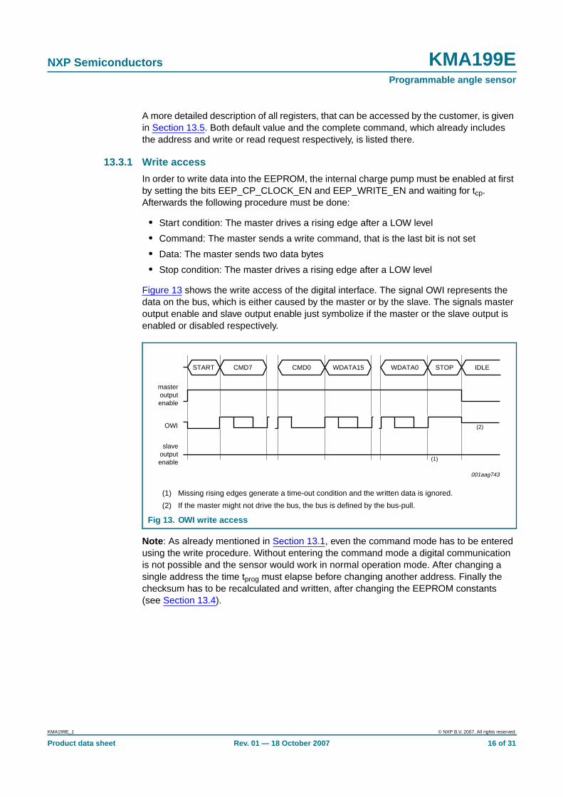
13.3.1 Write access
In order to write data into the EEPROM, the internal charge pump must be enabled at firstby setting the bits EEP_CP_CLOCK_EN and EEP_WRITE_EN and waiting for tcp.Afterwards the following procedure must be done:
• Start condition: The master drives a rising edge after a LOW level
• Command: The master sends a write command, that is the last bit is not set
• Data: The master sends two data bytes
• Stop condition: The master drives a rising edge after a LOW level
Figure 13 shows the write access of the digital interface. The signal OWI represents thedata on the bus, which is either caused by the master or by the slave. The signals masteroutput enable and slave output enable just symbolize if the master or the slave output isenabled or disabled respectively.
Note : As already mentioned in Section 13.1, even the command mode has to be enteredusing the write procedure. Without entering the command mode a digital communicationis not possible and the sensor would work in normal operation mode. After changing asingle address the time tprog must elapse before changing another address. Finally thechecksum has to be recalculated and written, after changing the EEPROM constants(see Section 13.4).
(1) Missing rising edges generate a time-out condition and the written data is ignored.
(2) If the master might not drive the bus, the bus is defined by the bus-pull.
Fig 13. OWI write access
001aag743
masteroutputenable
slaveoutputenable
START CMD7 CMD0 STOP
(1)
(2)
IDLEWDATA15 WDATA0
OWI
KMA199E_1 © NXP B.V. 2007. All rights reserved.
Product data sheet Rev. 01 — 18 October 2007 16 of 31
NXP Semiconductors KMA199EProgrammable angle sensor
13.3.2 Read access
In order to read data from the sensor, the following procedure must be done:
• Start condition: The master drives a rising edge after a LOW level
• Command: The master sends a read command, that is the last bit is set
• Handover: The master sends a handover bit, that is a logic 0 and disables his outputafter a three-quarter bit period
• Takeover: The slave drives a LOW level after the falling edge for ttko(slv)
• Data: The slave sends two data bytes
• Handover: The slave sends a handover bit, that is a logic 0 and disables his outputafter a three-quarter bit period
• Takeover: The master drives a LOW level after the falling edge for ttko(mas)
• Stop condition: The master drives a rising edge after a LOW level
Figure 14 shows the read access of the digital interface. The signal OWI represents thedata on the bus, which is either caused by the master or by the slave. The signals masteroutput enable and slave output enable just symbolize if the master or the slave output isenabled or disabled respectively.
(1) Duration of LOW level for slave takeover ttko(slv).
(2) There is an overlap in the output enables of master and slave, because both drive a LOW level.However this ensures the independency from having a pull-up or pull-down on the bus. Inaddition it improves the ElectroMagnetic Compatibility (EMC) robustness, because all levelsare actively driven.
(3) Duration of LOW level for master takeover ttko(mas).
(4) If the master does not take the bus and a pull-up exists, the stop condition is generated by thepull-up. Otherwise a time-out is generated if there is a pull-down and the slave waits for a risingedge as start condition.
(5) If the master might not drive the bus, the bus is defined by the bus-pull.
Fig 14. OWI read access
001aag744
masteroutputenable
slaveoutputenable
START CMD7 CMD0 RDATA0
(1)
(2) (2) (4)
(5)
(3)
HANDSHAKE HANDSHAKERDATA15 IDLESTOP
OWI
KMA199E_1 © NXP B.V. 2007. All rights reserved.
Product data sheet Rev. 01 — 18 October 2007 17 of 31
NXP Semiconductors KMA199EProgrammable angle sensor
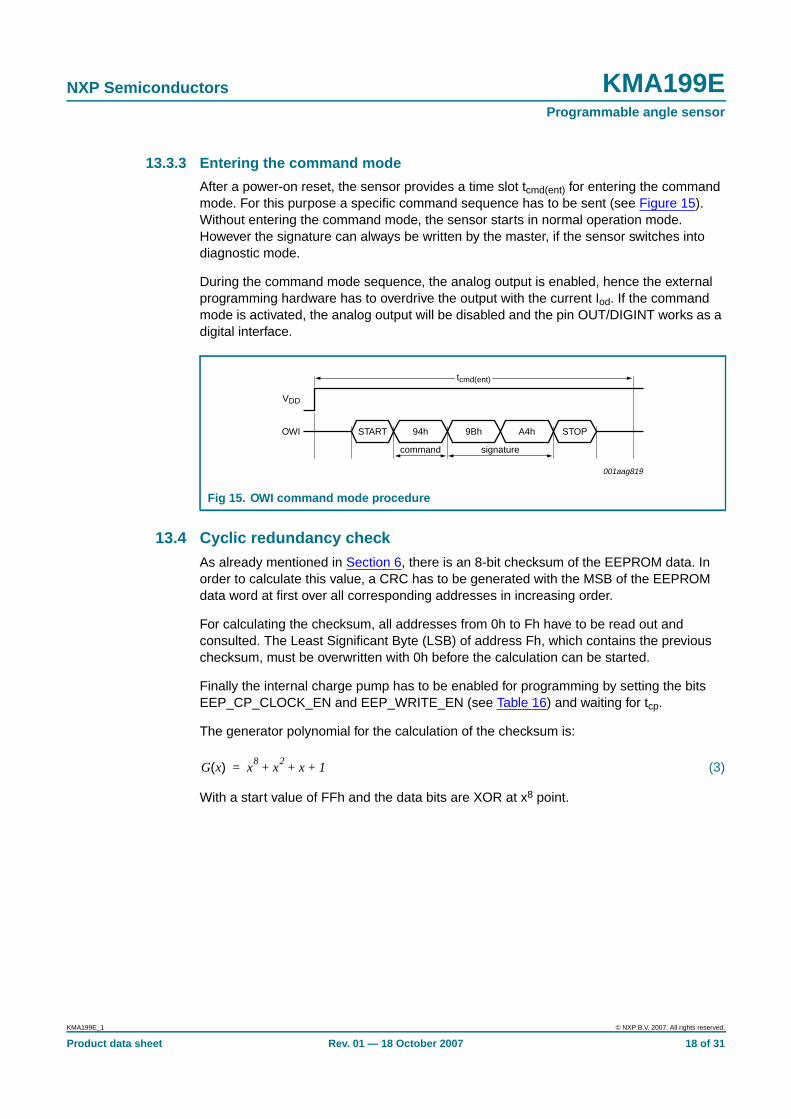
13.3.3 Entering the command mode
After a power-on reset, the sensor provides a time slot tcmd(ent) for entering the commandmode. For this purpose a specific command sequence has to be sent (see Figure 15).Without entering the command mode, the sensor starts in normal operation mode.However the signature can always be written by the master, if the sensor switches intodiagnostic mode.
During the command mode sequence, the analog output is enabled, hence the externalprogramming hardware has to overdrive the output with the current Iod. If the commandmode is activated, the analog output will be disabled and the pin OUT/DIGINT works as adigital interface.
13.4 Cyclic redundancy checkAs already mentioned in Section 6, there is an 8-bit checksum of the EEPROM data. Inorder to calculate this value, a CRC has to be generated with the MSB of the EEPROMdata word at first over all corresponding addresses in increasing order.
For calculating the checksum, all addresses from 0h to Fh have to be read out andconsulted. The Least Significant Byte (LSB) of address Fh, which contains the previouschecksum, must be overwritten with 0h before the calculation can be started.
Finally the internal charge pump has to be enabled for programming by setting the bitsEEP_CP_CLOCK_EN and EEP_WRITE_EN (see Table 16) and waiting for tcp.
The generator polynomial for the calculation of the checksum is:
(3)
With a start value of FFh and the data bits are XOR at x8 point.
Fig 15. OWI command mode procedure
001aag819
tcmd(ent)
signaturecommand
STARTOWI
VDD
94h 9Bh A4h STOP
G x( ) x8
x2
x 1+ + +=
KMA199E_1 © NXP B.V. 2007. All rights reserved.
Product data sheet Rev. 01 — 18 October 2007 18 of 31
NXP Semiconductors KMA199EProgrammable angle sensor
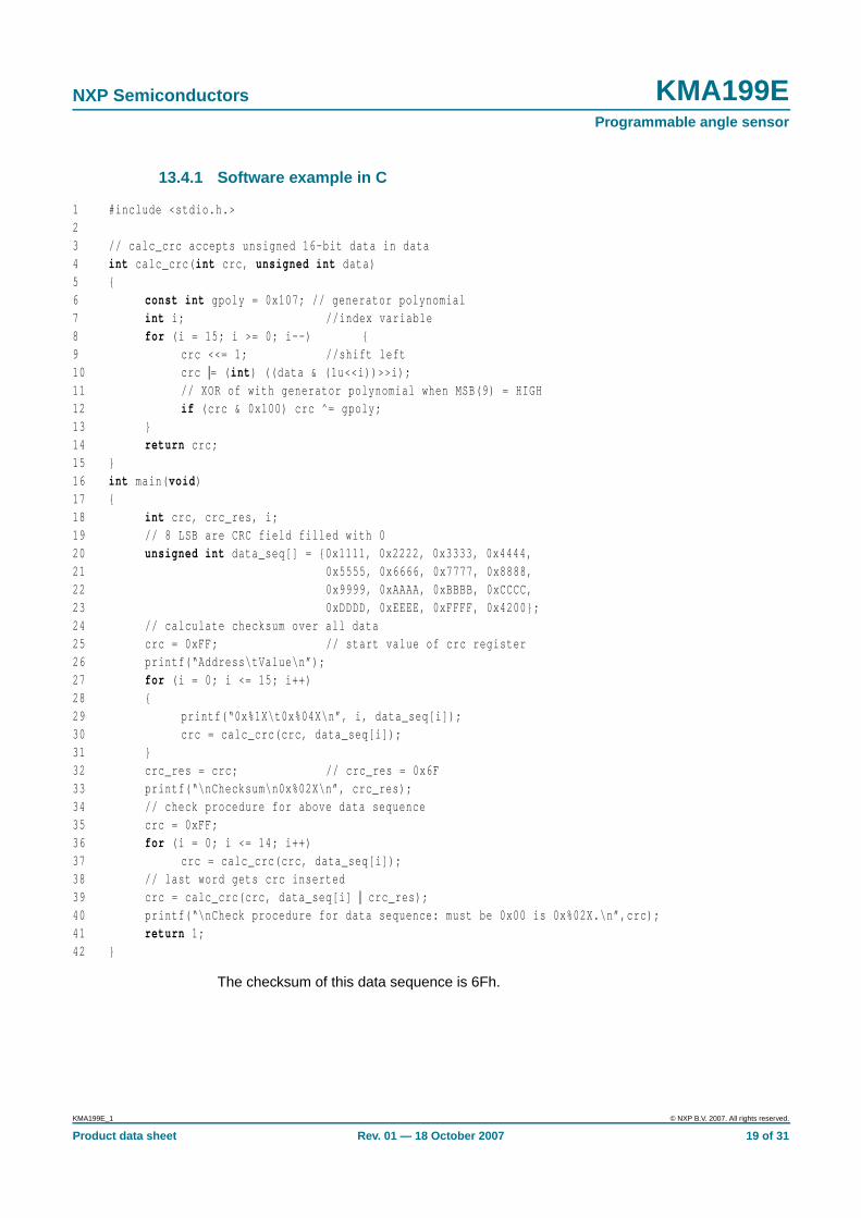
13.4.1 Software example in C
1 #include <stdio.h.>23 // calc_crc accepts unsigned 16-bit data in data4 int calc_crc( int crc, unsigned int data)5 6 const int gpoly = 0x107; / / generator polynomial7 int i ; / / index variable8 for ( i = 15; i >= 0; i--) 9 crc <<= 1; //shif t left10 crc |= ( int ) ((data & (1u<<i))>>i);11 // XOR of with generator polynomial when MSB(9) = HIGH12 i f (crc & 0x100) crc ^= gpoly;13 14 return crc;15 16 int main( void )17 18 int crc, crc_res, i ;19 // 8 LSB are CRC field f i l led with 020 unsigned int data_seq[] = 0x1111, 0x2222, 0x3333, 0x4444,21 0x5555, 0x6666, 0x7777, 0x8888,22 0x9999, 0xAAAA, 0xBBBB, 0xCCCC,23 0xDDDD, 0xEEEE, 0xFFFF, 0x4200;24 // calculate checksum over al l data25 crc = 0xFF; // start value of crc register26 printf(“Address\tValue\n”);27 for ( i = 0; i <= 15; i++)28 29 printf(“0x%1X\t0x%04X\n”, i , data_seq[i ]) ;30 crc = calc_crc(crc, data_seq[i ]) ;31 32 crc_res = crc; / / crc_res = 0x6F33 printf(“\nChecksum\n0x%02X\n”, crc_res);34 // check procedure for above data sequence35 crc = 0xFF;36 for ( i = 0; i <= 14; i++)37 crc = calc_crc(crc, data_seq[i ]) ;38 // last word gets crc inserted39 crc = calc_crc(crc, data_seq[i ] | crc_res);40 printf(“\nCheck procedure for data sequence: must be 0x00 is 0x%02X.\n”,crc);41 return 1;42
The checksum of this data sequence is 6Fh.
KMA199E_1 © NXP B.V. 2007. All rights reserved.
Product data sheet Rev. 01 — 18 October 2007 19 of 31
NXP Semiconductors KMA199EProgrammable angle sensor
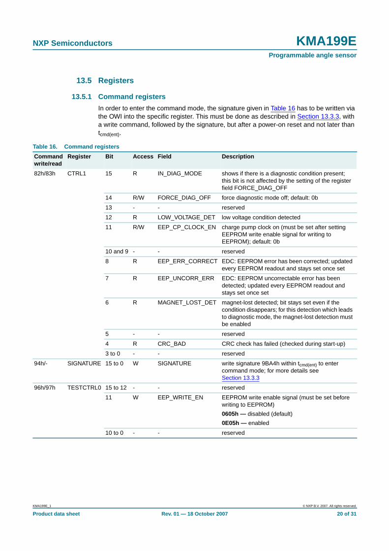
13.5 Registers
13.5.1 Command registers
In order to enter the command mode, the signature given in Table 16 has to be written viathe OWI into the specific register. This must be done as described in Section 13.3.3, witha write command, followed by the signature, but after a power-on reset and not later thantcmd(ent).
Table 16. Command registers
Commandwrite/read
Register Bit Access Field Description
82h/83h CTRL1 15 R IN_DIAG_MODE shows if there is a diagnostic condition present;this bit is not affected by the setting of the registerfield FORCE_DIAG_OFF
14 R/W FORCE_DIAG_OFF force diagnostic mode off; default: 0b
13 - - reserved
12 R LOW_VOLTAGE_DET low voltage condition detected
11 R/W EEP_CP_CLOCK_EN charge pump clock on (must be set after settingEEPROM write enable signal for writing toEEPROM); default: 0b
10 and 9 - - reserved
8 R EEP_ERR_CORRECT EDC: EEPROM error has been corrected; updatedevery EEPROM readout and stays set once set
7 R EEP_UNCORR_ERR EDC: EEPROM uncorrectable error has beendetected; updated every EEPROM readout andstays set once set
6 R MAGNET_LOST_DET magnet-lost detected; bit stays set even if thecondition disappears; for this detection which leadsto diagnostic mode, the magnet-lost detection mustbe enabled
5 - - reserved
4 R CRC_BAD CRC check has failed (checked during start-up)
3 to 0 - - reserved
94h/- SIGNATURE 15 to 0 W SIGNATURE write signature 9BA4h within tcmd(ent) to entercommand mode; for more details seeSection 13.3.3
96h/97h TESTCTRL0 15 to 12 - - reserved
11 W EEP_WRITE_EN EEPROM write enable signal (must be set beforewriting to EEPROM)
0605h — disabled (default)
0E05h — enabled
10 to 0 - - reserved
KMA199E_1 © NXP B.V. 2007. All rights reserved.
Product data sheet Rev. 01 — 18 October 2007 20 of 31
NXP Semiconductors KMA199EProgrammable angle sensor
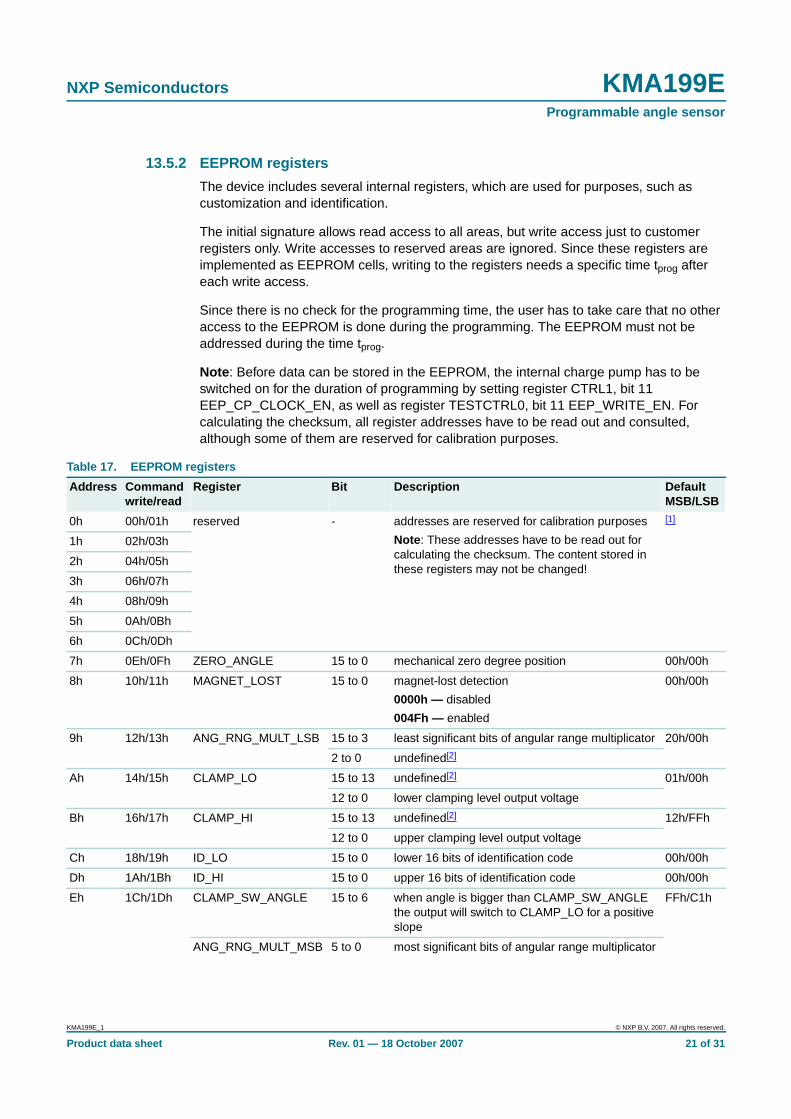
13.5.2 EEPROM registers
The device includes several internal registers, which are used for purposes, such ascustomization and identification.
The initial signature allows read access to all areas, but write access just to customerregisters only. Write accesses to reserved areas are ignored. Since these registers areimplemented as EEPROM cells, writing to the registers needs a specific time tprog aftereach write access.
Since there is no check for the programming time, the user has to take care that no otheraccess to the EEPROM is done during the programming. The EEPROM must not beaddressed during the time tprog.
Note : Before data can be stored in the EEPROM, the internal charge pump has to beswitched on for the duration of programming by setting register CTRL1, bit 11EEP_CP_CLOCK_EN, as well as register TESTCTRL0, bit 11 EEP_WRITE_EN. Forcalculating the checksum, all register addresses have to be read out and consulted,although some of them are reserved for calibration purposes.
Table 17. EEPROM registers
Address Commandwrite/read
Register Bit Description DefaultMSB/LSB
0h 00h/01h reserved - addresses are reserved for calibration purposes
Note : These addresses have to be read out forcalculating the checksum. The content stored inthese registers may not be changed!
[1]
1h 02h/03h
2h 04h/05h
3h 06h/07h
4h 08h/09h
5h 0Ah/0Bh
6h 0Ch/0Dh
7h 0Eh/0Fh ZERO_ANGLE 15 to 0 mechanical zero degree position 00h/00h
8h 10h/11h MAGNET_LOST 15 to 0 magnet-lost detection
0000h — disabled
004Fh — enabled
00h/00h
9h 12h/13h ANG_RNG_MULT_LSB 15 to 3 least significant bits of angular range multiplicator 20h/00h
2 to 0 undefined[2]
Ah 14h/15h CLAMP_LO 15 to 13 undefined[2] 01h/00h
12 to 0 lower clamping level output voltage
Bh 16h/17h CLAMP_HI 15 to 13 undefined[2] 12h/FFh
12 to 0 upper clamping level output voltage
Ch 18h/19h ID_LO 15 to 0 lower 16 bits of identification code 00h/00h
Dh 1Ah/1Bh ID_HI 15 to 0 upper 16 bits of identification code 00h/00h
Eh 1Ch/1Dh CLAMP_SW_ANGLE 15 to 6 when angle is bigger than CLAMP_SW_ANGLEthe output will switch to CLAMP_LO for a positiveslope
FFh/C1h
ANG_RNG_MULT_MSB 5 to 0 most significant bits of angular range multiplicator
KMA199E_1 © NXP B.V. 2007. All rights reserved.
Product data sheet Rev. 01 — 18 October 2007 21 of 31
NXP Semiconductors KMA199EProgrammable angle sensor
[1] Variable and individual for each device.
[2] Undefined; must be written as zero for default.
Mechanical angular range 0000h = 0° to FFFFh = 180° − 1 LSB
Examples:
• Mechanical zero angle 0° = 0000h
• Mechanical zero angle 10° = 0E38h
• Mechanical zero angle 45° = 4000h
[1] Undefined; must be written as zero for default and may return any value when read.
(4)
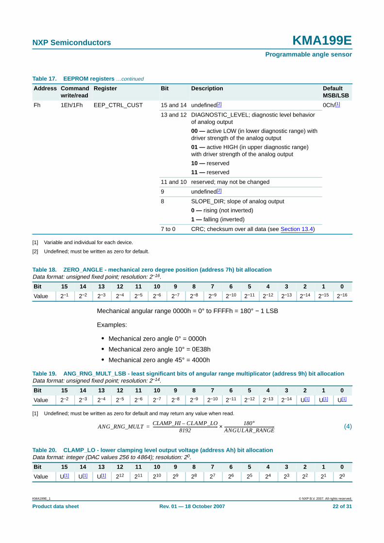
Fh 1Eh/1Fh EEP_CTRL_CUST 15 and 14 undefined[2] 0Ch/[1]
13 and 12 DIAGNOSTIC_LEVEL; diagnostic level behaviorof analog output
00 — active LOW (in lower diagnostic range) withdriver strength of the analog output
01 — active HIGH (in upper diagnostic range)with driver strength of the analog output
10 — reserved
11 — reserved
11 and 10 reserved; may not be changed
9 undefined[2]
8 SLOPE_DIR; slope of analog output
0 — rising (not inverted)
1 — falling (inverted)
7 to 0 CRC; checksum over all data (see Section 13.4)
Table 17. EEPROM registers …continued
Address Commandwrite/read
Register Bit Description DefaultMSB/LSB
Table 18. ZERO_ANGLE - mechanical zero degree position (address 7h) bit allocationData format: unsigned fixed point; resolution: 2−16.
Bit 15 14 13 12 11 10 9 8 7 6 5 4 3 2 1 0
Value 2−1 2−2 2−3 2−4 2−5 2−6 2−7 2−8 2−9 2−10 2−11 2−12 2−13 2−14 2−15 2−16
Table 19. ANG_RNG_MULT_LSB - least significant bits of angular range multiplicator (address 9h) bit allocationData format: unsigned fixed point; resolution: 2−14.
Bit 15 14 13 12 11 10 9 8 7 6 5 4 3 2 1 0
Value 2−2 2−3 2−4 2−5 2−6 2−7 2−8 2−9 2−10 2−11 2−12 2−13 2−14 U[1] U[1] U[1]
ANG_RNG_MULTCLAMP_HI CLAMP_LO–
8192-------------------------------------------------------------------
180°ANGULAR_RANGE----------------------------------------------------×=
Table 20. CLAMP_LO - lower clamping level output voltage (address Ah) bit allocationData format: integer (DAC values 256 to 4864); resolution: 20.
Bit 15 14 13 12 11 10 9 8 7 6 5 4 3 2 1 0
Value U[1] U[1] U[1] 212 211 210 29 28 27 26 25 24 23 22 21 20
KMA199E_1 © NXP B.V. 2007. All rights reserved.
Product data sheet Rev. 01 — 18 October 2007 22 of 31
NXP Semiconductors KMA199EProgrammable angle sensor
[1] Undefined; must be written as zero for default and may return any value when read.
Values 0 to 255 are reserved. It is not permitted to use such values.
Examples:
• 100 %VDD = 5120 (reserved)
• 10 %VDD = 512
• 5 %VDD = 256
[1] Undefined; must be written as zero for default and may return any value when read.
Values 4865 to 5120 are reserved. It is not permitted to use such values.
Examples:
• 100 %VDD = 5120 (reserved)
• 95 %VDD = 4864
• 90 %VDD = 4608
(5)
Examples:
•
•
Mechanical angular range 0000h = 0° to 3FFh = 180° − 1 LSB.
(6)
If the magnetic field angle is larger than the CLAMP_SW_ANGLE, the output will switch toCLAMP_LO for a positive slope. The value of CLAMP_SW_ANGLE can be calculatedfrom other EEPROM constants, but must be programmed.
Table 21. CLAMP_HI - upper clamping level output voltage (address Bh) bit allocationData format: integer (DAC values 256 to 4864); resolution: 20.
Bit 15 14 13 12 11 10 9 8 7 6 5 4 3 2 1 0
Value U[1] U[1] U[1] 212 211 210 29 28 27 26 25 24 23 22 21 20
Table 22. ANG_RNG_MULT_MSB - most significant bits of angular range multiplicator (address Eh) bit allocationData format: unsigned fixed point.
Bit 15 14 13 12 11 10 9 8 7 6 5 4 3 2 1 0
Value CLAMP_SW_ANGLE 24 23 22 21 20 2−1
ANG_RNG_MULTCLAMP_HI CLAMP_LO–
8192-------------------------------------------------------------------
180°ANGULAR_RANGE----------------------------------------------------×=
ANG_RNG_MULT4864 256–
8192---------------------------
180°180°-----------× 0.5625= =
ANG_RNG_MULT4864 256–
8192---------------------------
90°180°-----------× 1.125= =
Table 23. CLAMP_SW_ANGLE - clamp switch angle (address Eh) bit allocationData format: unsigned fixed point.
Bit 15 14 13 12 11 10 9 8 7 6 5 4 3 2 1 0
Value 2−1 2−2 2−3 2−4 2−5 2−6 2−7 2−8 2−9 2−10 ANG_RNG_MULT_MSB
CLAMP_SW_ANGLE12--- 1
CLAMP_HI CLAMP_LO–8192
--------------------------------------------------------------------1
ANG_RNG_MULT-----------------------------------------------×+
×=
KMA199E_1 © NXP B.V. 2007. All rights reserved.
Product data sheet Rev. 01 — 18 October 2007 23 of 31
NXP Semiconductors KMA199EProgrammable angle sensor
14. Electromagnetic compatibility
EMC is achieved by the KMA199E.
14.1 Emission (CISPR 25)Tests according to CISPR 25 were fulfilled.
14.1.1 Conducted radio disturbance
Test of the device according to CISPR 25, chapter 11 (artificial network).
Class: 5.
14.1.2 Radiated radio disturbance
Test of the device according to CISPR 25, chapter 13 (anechoic chamber -component/module).
Class: 5 (without addition of 6 dB in FM band).
14.2 Radiated disturbances (ISO 11452-2, ISO 11452-4 and ISO 11452-5)The common understanding of the requested function is that an effect is tolerated asdescribed in Table 24 during the disturbance. If the KMA199E operates in operationmode, the Radio Frequency (RF) noise will occur on the signal and supply line.
14.2.1 Absorber lined shielded enclosure
Tests according to ISO 11452-2 were fulfilled.
Test levels:
> 200 V/m 200 MHz to 400 MHz (step 10 MHz)
> 200 V/m 400 MHz to 1000 MHz (step 25 MHz)
> 200 V/m 1 GHz to 10 GHz (step 100 MHz)
Modulation: Continuous Wave (CW); AM: 1 kHz, 80 %.
State: A.
14.2.2 Bulk-current injection
Tests according to ISO 11452-4 were fulfilled.
Test level: 200 mA with CL = 1 nF.
State: A.
14.2.3 Strip line
Tests according to ISO 11452-5 were fulfilled.
Table 24. Failure condition for radiated disturbances
Parameter Comment Min Max Unit
Variation of output signal in analogoutput mode
value measured relative to theoutput at test start
- ±0.9 %VDD
KMA199E_1 © NXP B.V. 2007. All rights reserved.
Product data sheet Rev. 01 — 18 October 2007 24 of 31
NXP Semiconductors KMA199EProgrammable angle sensor
Test level: 200 V/m with CL = 1 nF.
State: A.
In deviation of ISO 11452-5 the measurement must be taken up to 1 GHz.
14.2.4 Immunity against mobile phones
Tests according to ISO 11452-2 were fulfilled.
State: A.
Definition of Global System for Mobile Communications (GSM) signal:
• Pulse modulation: per GSM specification (217 Hz; 12.5 % duty cycle)
• Modulation grade: ≥ 60 dB
• Sweep: linear 800 MHz to 3 GHz (duration 10 s at 890 MHz, 940 MHz and 1.8 GHzband)
• Antenna polarization: vertical, horizontal
• Field strength: 200 V/m during on-time (calibration in CW)
In deviation of ISO 11452-2 a GSM signal (definition see above) instead of an AM signalwas used.
14.3 Transients - pulses (ISO 7637-1 and ISO 7637-3)The KMA199E is designed for a stabilized 5 V supply. To raise immunity againstnon-galvanic coupled transient pulses, protection diodes are implemented into theKMA199E.
For applications with disturbances by capacitive or inductive coupling on supply line orradiated disturbances an application circuit is recommended. Applications with thisarrangement passed the EMC tests according to the product standard 1 (electricaltransient transmission by capacitive or inductive coupling) and standard 3 (radiateddisturbances).
The common understanding of the requested function is that an effect is tolerated asdescribed in Table 25 during the disturbance. Class C means that the device goes intoreset or diagnostic mode and comes back after disturbances. If the KMA199E operates innormal operation mode, the test pulses are visible on the signal line. A protection circuit isused. The KMA199E is directly supplied with 5 V.
14.3.1 Coupled
Tests according to ISO 7637-3 were fulfilled.
Level of pulses: IV (−60 V for pulse 3a and +40 V for pulse 3b).
Class: B for pulse 3a, B for pulse 3b.
Table 25. Failure condition for transients
Parameter Comment Min Max Unit
Variation of output signal after exposure topulses in analog output mode
value measured relative tothe output at test start
- ±0.9 %VDD
KMA199E_1 © NXP B.V. 2007. All rights reserved.
Product data sheet Rev. 01 — 18 October 2007 25 of 31
NXP Semiconductors KMA199EProgrammable angle sensor
Test time: 10 min.
Transient transmission by capacitive and inductive coupling via lines other than supplylines (interface, analog output) have to be tolerated according to ISO 7637-3 (pulses 3aand 3b).
15. ElectroStatic Discharge (ESD)
To raise immunity against ESD pulses, protection diodes are implemented into theKMA199E.
15.1 Human body modelThe KMA199E must not be damaged at 8 kV, according to the human body model at100 pF and 1.5 kΩ. The test is according to AEC-Q100, Rev-E, method 002. Thisprotection must be ensured at all external pins (OUT/DIGINT, VDD and GND).
Furthermore all interconnects (pins between package head and package body) must notbe damaged at 2 kV, according to AEC-Q100, Rev-E, method 002.
15.2 Machine modelThe KMA199E must not be damaged at 400 V, according to the machine model. The testis according to AEC-Q100, Rev-E, method 003. This protection must be ensured at allexternal pins (OUT/DIGINT, VDD and GND).
Furthermore all interconnects (pins between package head and package body) must notbe damaged at 200 V, according to AEC-Q100, Rev-E, method 003.
All pins have a latch-up protection.
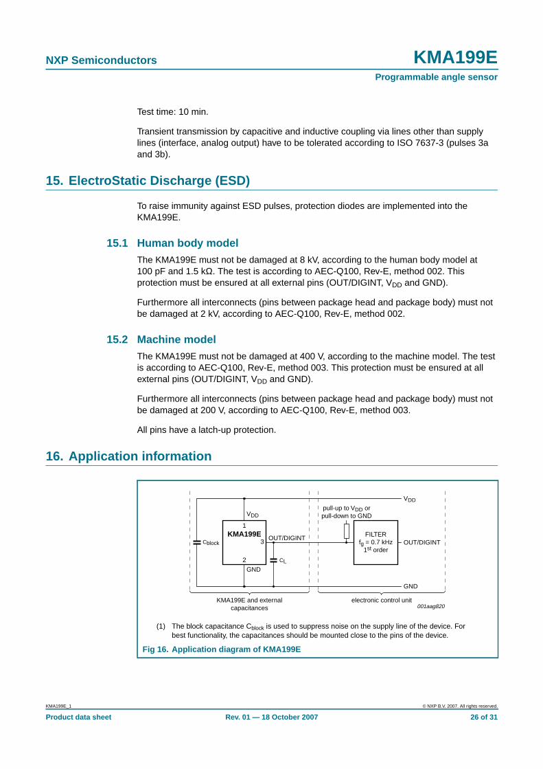
16. Application information
(1) The block capacitance Cblock is used to suppress noise on the supply line of the device. Forbest functionality, the capacitances should be mounted close to the pins of the device.
Fig 16. Application diagram of KMA199E
001aag820
2
3
VDD
GND
OUT/DIGINT
KMA199E and externalcapacitances
electronic control unit
VDD
GND
OUT/DIGINT
1
pull-up to VDD orpull-down to GND
Cblock
CL
KMA199E FILTERfg = 0.7 kHz
1st order
KMA199E_1 © NXP B.V. 2007. All rights reserved.
Product data sheet Rev. 01 — 18 October 2007 26 of 31
NXP Semiconductors KMA199EProgrammable angle sensor
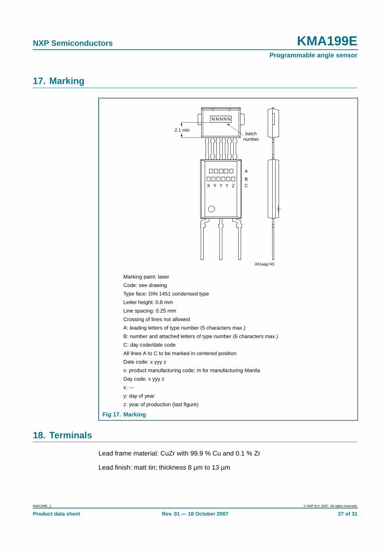
17. Marking
18. Terminals
Lead frame material: CuZr with 99.9 % Cu and 0.1 % Zr
Lead finish: matt tin; thickness 8 µm to 13 µm
Marking paint: laser
Code: see drawing
Type face: DIN 1451 condensed type
Letter height: 0.8 mm
Line spacing: 0.25 mm
Crossing of lines not allowed
A: leading letters of type number (5 characters max.)
B: number and attached letters of type number (6 characters max.)
C: day code/date code
All lines A to C to be marked in centered position
Date code: x yyy z
x: product manufacturing code; m for manufacturing Manila
Day code: x yyy z
x: ---
y: day of year
z: year of production (last figure)
Fig 17. Marking
001aag745
batchnumber
2.1 min
X
N NNNN
Y CB
A
Y Y Z
KMA199E_1 © NXP B.V. 2007. All rights reserved.
Product data sheet Rev. 01 — 18 October 2007 27 of 31
NXP Semiconductors KMA199EProgrammable angle sensor
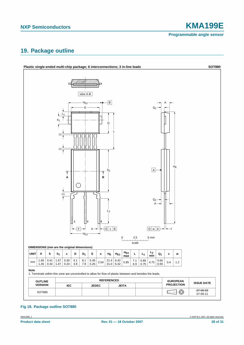
19. Package outline
Fig 18. Package outline SOT880
SOT880Plastic single-ended multi-chip package; 6 interconnections; 3 in-line leads
UNIT b c L2min
REFERENCESOUTLINEVERSION
EUROPEANPROJECTION ISSUE DATE
IEC JEDEC JEITA
mm 1.651.45
0.410.34
b1
1.571.47
8.17.9
4.13.9
0.300.24 4.75
L1L
7.16.9
0.850.75
wvD D1
5.455.25
E
2.5421.421.0
HE
6.426.32 5.85 1.20.4
HE1HE2max
e Q1
0.650.55
DIMENSIONS (mm are the original dimensions)
SOT88007-09-0307-09-11
A
0 2.5 5 mm
scale
view A-B
Note1. Terminals within this zone are uncontrolled to allow for flow of plastic between and besides the leads.
HE
c
Q1
Q1
A
A
A
w Ae
B
E
(1)
(1)
(1)
HE1
HE2
L1
L
b1D
D1
L2
b
1 2 3
BA
v B
KMA199E_1 © NXP B.V. 2007. All rights reserved.
Product data sheet Rev. 01 — 18 October 2007 28 of 31
NXP Semiconductors KMA199EProgrammable angle sensor
20. Handling information
21. Solderability information
The solderability qualification is done according to AEC-Q100, Rev-E. Recommendedsoldering process for leaded devices is wave soldering. The maximum solderingtemperature is 260 °C for maximum 5 s. Device terminals shall be compatible with laserand electrical welding.
22. Revision history
Dimensions in mm
(1) No bending allowed.
(2) Plastic body and interface plastic body - leads: application of bending forces not allowed.
Fig 19. Bending recommendation
006aaa246
R 0.25 min
R 0.25 min
0.7(1)
0.7(1)
0.7(1)
(2)
(2)
Table 26. Revision history
Document ID Release date Data sheet status Change notice Supersedes
KMA199E_1 20071018 Product data sheet - -
KMA199E_1 © NXP B.V. 2007. All rights reserved.
Product data sheet Rev. 01 — 18 October 2007 29 of 31

NXP Semiconductors KMA199EProgrammable angle sensor
23. Legal information
23.1 Data sheet status
[1] Please consult the most recently issued document before initiating or completing a design.
[2] The term ‘short data sheet’ is explained in section “Definitions”.
[3] The product status of device(s) described in this document may have changed since this document was published and may differ in case of multiple devices. The latest product statusinformation is available on the Internet at URL http://www.nxp.com.
23.2 Definitions
Draft — The document is a draft version only. The content is still underinternal review and subject to formal approval, which may result inmodifications or additions. NXP Semiconductors does not give anyrepresentations or warranties as to the accuracy or completeness ofinformation included herein and shall have no liability for the consequences ofuse of such information.
Short data sheet — A short data sheet is an extract from a full data sheetwith the same product type number(s) and title. A short data sheet is intendedfor quick reference only and should not be relied upon to contain detailed andfull information. For detailed and full information see the relevant full datasheet, which is available on request via the local NXP Semiconductors salesoffice. In case of any inconsistency or conflict with the short data sheet, thefull data sheet shall prevail.
23.3 Disclaimers
General — Information in this document is believed to be accurate andreliable. However, NXP Semiconductors does not give any representations orwarranties, expressed or implied, as to the accuracy or completeness of suchinformation and shall have no liability for the consequences of use of suchinformation.
Right to make changes — NXP Semiconductors reserves the right to makechanges to information published in this document, including withoutlimitation specifications and product descriptions, at any time and withoutnotice. This document supersedes and replaces all information supplied priorto the publication hereof.
Suitability for use — NXP Semiconductors products are not designed,authorized or warranted to be suitable for use in medical, military, aircraft,space or life support equipment, nor in applications where failure or
malfunction of a NXP Semiconductors product can reasonably be expected toresult in personal injury, death or severe property or environmental damage.NXP Semiconductors accepts no liability for inclusion and/or use of NXPSemiconductors products in such equipment or applications and thereforesuch inclusion and/or use is at the customer’s own risk.
Applications — Applications that are described herein for any of theseproducts are for illustrative purposes only. NXP Semiconductors makes norepresentation or warranty that such applications will be suitable for thespecified use without further testing or modification.
Limiting values — Stress above one or more limiting values (as defined inthe Absolute Maximum Ratings System of IEC 60134) may cause permanentdamage to the device. Limiting values are stress ratings only and operation ofthe device at these or any other conditions above those given in theCharacteristics sections of this document is not implied. Exposure to limitingvalues for extended periods may affect device reliability.
Terms and conditions of sale — NXP Semiconductors products are soldsubject to the general terms and conditions of commercial sale, as publishedat http://www.nxp.com/profile/terms, including those pertaining to warranty,intellectual property rights infringement and limitation of liability, unlessexplicitly otherwise agreed to in writing by NXP Semiconductors. In case ofany inconsistency or conflict between information in this document and suchterms and conditions, the latter will prevail.
No offer to sell or license — Nothing in this document may be interpretedor construed as an offer to sell products that is open for acceptance or thegrant, conveyance or implication of any license under any copyrights, patentsor other industrial or intellectual property rights.
23.4 TrademarksNotice: All referenced brands, product names, service names and trademarksare the property of their respective owners.
24. Contact information
For additional information, please visit: http://www .nxp.com
For sales office addresses, send an email to: salesad [email protected]
Document status [1] [2] Product status [3] Definition
Objective [short] data sheet Development This document contains data from the objective specification for product development.
Preliminary [short] data sheet Qualification This document contains data from the preliminary specification.
Product [short] data sheet Production This document contains the product specification.
KMA199E_1 © NXP B.V. 2007. All rights reserved.
Product data sheet Rev. 01 — 18 October 2007 30 of 31
NXP Semiconductors KMA199EProgrammable angle sensor
25. Contents
1 Product profile . . . . . . . . . . . . . . . . . . . . . . . . . . 11.1 General description. . . . . . . . . . . . . . . . . . . . . . 11.2 Features . . . . . . . . . . . . . . . . . . . . . . . . . . . . . . 12 Pinning information . . . . . . . . . . . . . . . . . . . . . . 23 Ordering information . . . . . . . . . . . . . . . . . . . . . 24 Functional diagram . . . . . . . . . . . . . . . . . . . . . . 35 Functional description . . . . . . . . . . . . . . . . . . . 45.1 Angular measurement directions . . . . . . . . . . . 46 Diagnostic features . . . . . . . . . . . . . . . . . . . . . . 56.1 EEPROM CRC and EDC supervision. . . . . . . . 56.2 Magnet-lost detection . . . . . . . . . . . . . . . . . . . . 56.3 Power-lost detection . . . . . . . . . . . . . . . . . . . . . 66.4 Low supply voltage detection . . . . . . . . . . . . . . 67 Analog output. . . . . . . . . . . . . . . . . . . . . . . . . . . 78 Limiting values. . . . . . . . . . . . . . . . . . . . . . . . . . 89 Recommended operating conditions. . . . . . . . 810 Thermal characteristics. . . . . . . . . . . . . . . . . . . 811 Characteristics . . . . . . . . . . . . . . . . . . . . . . . . . . 912 Definition of errors. . . . . . . . . . . . . . . . . . . . . . 1112.1 General . . . . . . . . . . . . . . . . . . . . . . . . . . . . . . 1112.2 Hysteresis error . . . . . . . . . . . . . . . . . . . . . . . 1112.3 Linearity error . . . . . . . . . . . . . . . . . . . . . . . . . 1212.4 Microlinearity error . . . . . . . . . . . . . . . . . . . . . 1212.5 Temperature drift error . . . . . . . . . . . . . . . . . . 1313 Programming . . . . . . . . . . . . . . . . . . . . . . . . . . 1313.1 General description. . . . . . . . . . . . . . . . . . . . . 1313.2 Timing characteristics . . . . . . . . . . . . . . . . . . . 1413.3 Sending and receiving data . . . . . . . . . . . . . . 1513.3.1 Write access . . . . . . . . . . . . . . . . . . . . . . . . . . 1613.3.2 Read access . . . . . . . . . . . . . . . . . . . . . . . . . . 1713.3.3 Entering the command mode . . . . . . . . . . . . . 1813.4 Cyclic redundancy check . . . . . . . . . . . . . . . . 1813.4.1 Software example in C . . . . . . . . . . . . . . . . . . 1913.5 Registers. . . . . . . . . . . . . . . . . . . . . . . . . . . . . 2013.5.1 Command registers . . . . . . . . . . . . . . . . . . . . 2013.5.2 EEPROM registers . . . . . . . . . . . . . . . . . . . . . 2114 Electromagnetic compatibility . . . . . . . . . . . . 2414.1 Emission (CISPR 25) . . . . . . . . . . . . . . . . . . . 2414.1.1 Conducted radio disturbance . . . . . . . . . . . . . 2414.1.2 Radiated radio disturbance. . . . . . . . . . . . . . . 2414.2 Radiated disturbances (ISO 11452-2,
ISO 11452-4 and ISO 11452-5) . . . . . . . . . . . 2414.2.1 Absorber lined shielded enclosure . . . . . . . . . 2414.2.2 Bulk-current injection . . . . . . . . . . . . . . . . . . . 2414.2.3 Strip line . . . . . . . . . . . . . . . . . . . . . . . . . . . . . 24
14.2.4 Immunity against mobile phones . . . . . . . . . . 2514.3 Transients - pulses (ISO 7637-1 and
ISO 7637-3) . . . . . . . . . . . . . . . . . . . . . . . . . . 2514.3.1 Coupled . . . . . . . . . . . . . . . . . . . . . . . . . . . . . 2515 ElectroStatic Discharge (ESD) . . . . . . . . . . . . 2615.1 Human body model . . . . . . . . . . . . . . . . . . . . 2615.2 Machine model. . . . . . . . . . . . . . . . . . . . . . . . 2616 Application information . . . . . . . . . . . . . . . . . 2617 Marking. . . . . . . . . . . . . . . . . . . . . . . . . . . . . . . 2718 Terminals . . . . . . . . . . . . . . . . . . . . . . . . . . . . . 2719 Package outline . . . . . . . . . . . . . . . . . . . . . . . . 2820 Handling information . . . . . . . . . . . . . . . . . . . 2921 Solderability information . . . . . . . . . . . . . . . . 2922 Revision history . . . . . . . . . . . . . . . . . . . . . . . 2923 Legal information . . . . . . . . . . . . . . . . . . . . . . 3023.1 Data sheet status . . . . . . . . . . . . . . . . . . . . . . 3023.2 Definitions . . . . . . . . . . . . . . . . . . . . . . . . . . . 3023.3 Disclaimers. . . . . . . . . . . . . . . . . . . . . . . . . . . 3023.4 Trademarks . . . . . . . . . . . . . . . . . . . . . . . . . . 3024 Contact information . . . . . . . . . . . . . . . . . . . . 3025 Contents. . . . . . . . . . . . . . . . . . . . . . . . . . . . . . 31
© NXP B.V. 2007. All rights reserved.For more information, please visit: http://www.nxp.comFor sales office addresses, please send an email to: [email protected]
Date of release: 18 October 2007
Document identifier: KMA199E_1
Please be aware that important notices concerning this document and the product(s)described herein, have been included in section ‘Legal information’.