Embed Size (px)
Citation preview
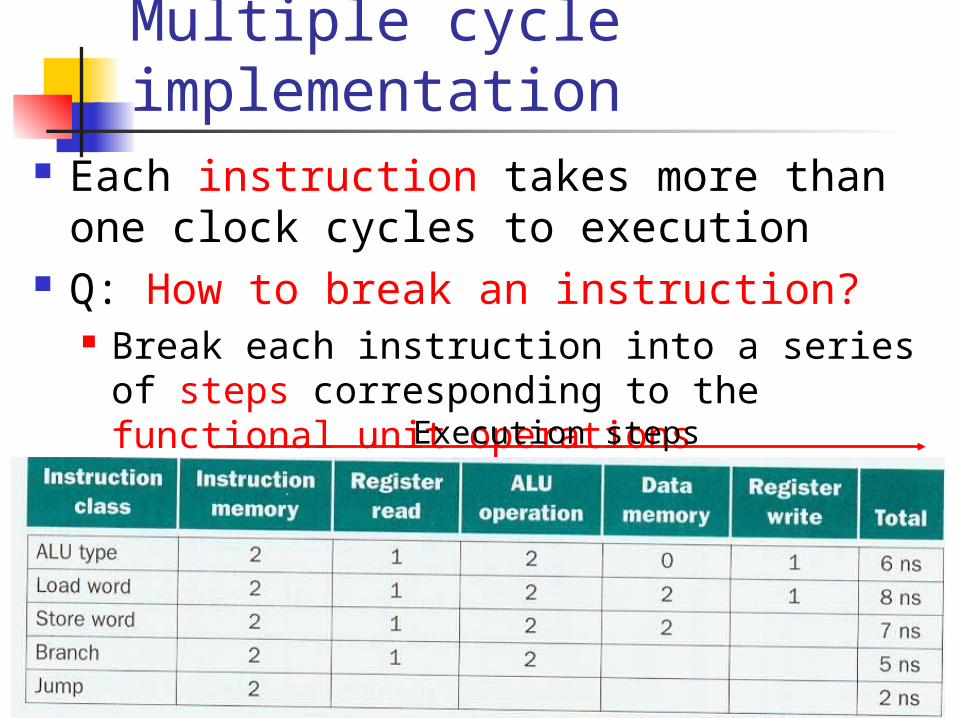
Multiple cycle implementation
Each instruction takes more than one clock cycles to execution
Q: How to break an instruction? Break each instruction into a series of
steps corresponding to the functional unit operations Execution steps
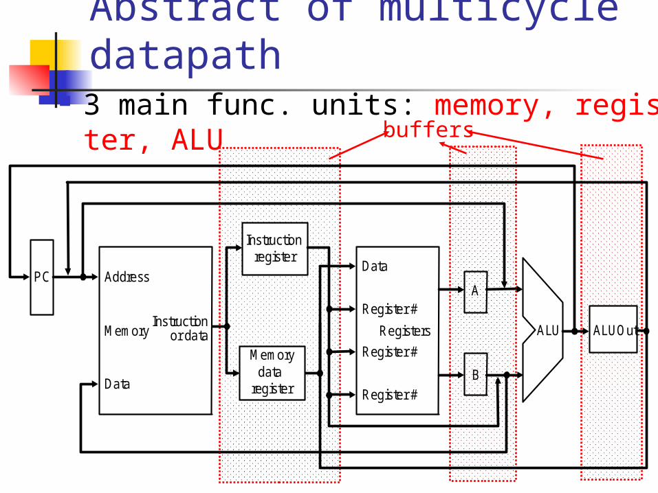
Abstract of multicycle datapath
3 main func. units: memory, register, ALU
PC
Memory
Address
Instructionor data
Data
Instructionregister
Registers
Register #
Data
Register #
Register #
ALU
Memorydata
register
A
B
ALUOut
buffers
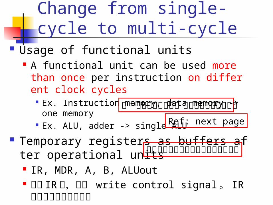
Change from single-cycle to multi-cycle
Usage of functional units A functional unit can be used more than on
ce per instruction on different clock cycles Ex. Instruction memory, data memory -> one m
emory Ex. ALU, adder -> single ALU
Temporary registers as buffers after operational units IR, MDR, A, B, ALUout 除了 IR 外,不需 write control signal 。 IR
需保存指令至指令結束
Ref: next page
同一功能單元可在同一指令的不同時脈中使用
不同時脈間的執行結果需存在暫存器中
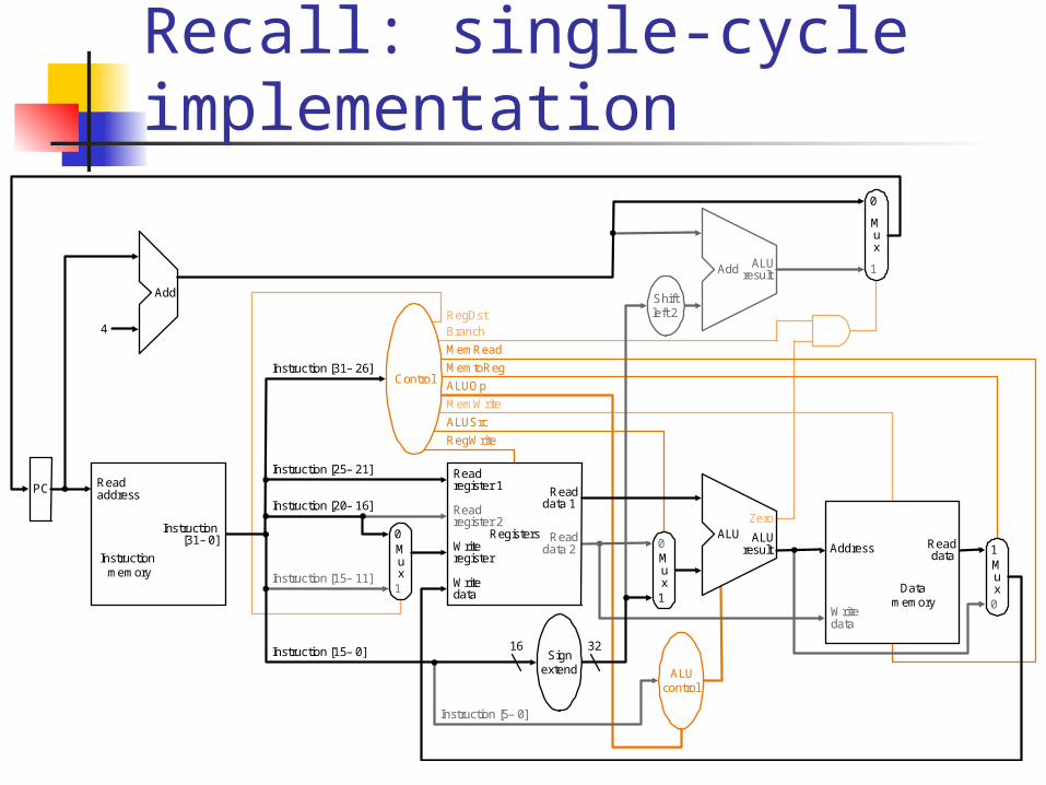
Recall: single-cycle implementation
PC
Instructionmemory
Readaddress
Instruction[31– 0]
Instruction [15– 11]
Instruction [20– 16]
Instruction [25– 21]
Add
Instruction [5– 0]
MemtoReg
ALUOp
MemWrite
RegWrite
MemRead
BranchRegDst
ALUSrc
Instruction [31– 26]
4
16 32Instruction [15– 0]
0
0Mux
0
1
ALUcontrol
Control
Shiftleft 2
Add ALUresult
Mux
0
1
RegistersWriteregister
Writedata
Readdata 1
Readdata 2
Readregister 1
Readregister 2
Signextend
Mux
1
ALUresult
Zero
Datamemory
Writedata
Readdata
Mux
1ALU
Address
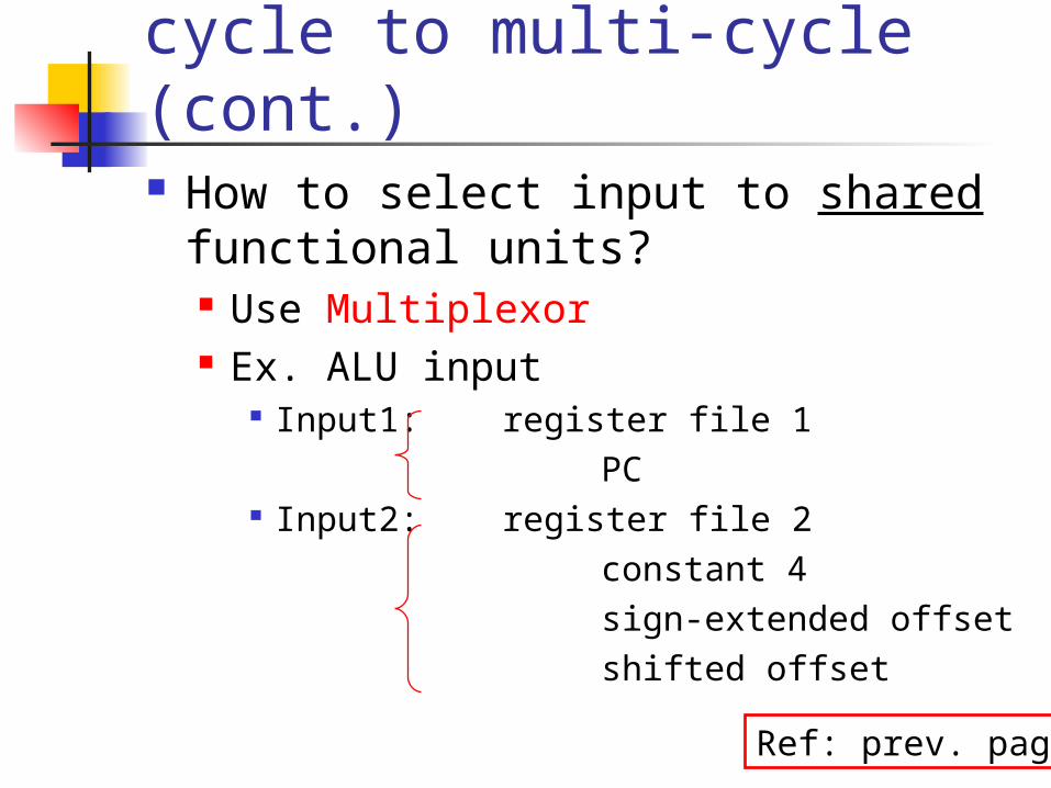
Change from single-cycle to multi-cycle (cont.) How to select input to shared functio
nal units? Use Multiplexor Ex. ALU input
Input1: register file 1 PC Input2: register file 2 constant 4 sign-extended offset shifted offset
Ref: prev. page
Shiftleft 2
PC
Memory
MemData
Writedata
Mux
0
1
RegistersWriteregister
Writedata
Readdata 1
Readdata 2
Readregister 1
Readregister 2
Mux
0
1
Mux
0
1
4
Instruction[15– 0]
Signextend
3216
Instruction[25– 21]
Instruction[20– 16]
Instruction[15– 0]
Instructionregister
1 Mux
0
3
2
Mux
ALUresult
ALUZero
Memorydata
register
Instruction[15– 11]
A
B
ALUOut
0
1
Address
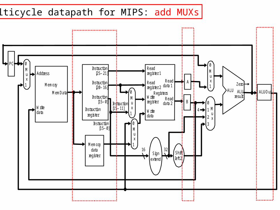
Multicycle datapath for MIPS: add MUXs
Shiftleft 2
MemtoReg
IorD MemRead MemWrite
PC
Memory
MemData
Writedata
Mux
0
1
RegistersWriteregister
Writedata
Readdata 1
Readdata 2
Readregister 1
Readregister 2
Instruction[15– 11]
Mux
0
1
Mux
0
1
4
ALUOpALUSrcB
RegDst RegWrite
Instruction[15– 0]
Instruction [5– 0]
Signextend
3216
Instruction[25– 21]
Instruction[20– 16]
Instruction[15– 0]
Instructionregister
1 Mux
0
3
2
ALUcontrol
Mux
0
1ALU
resultALU
ALUSrcA
ZeroA
B
ALUOut
IRWrite
Address
Memorydata
register
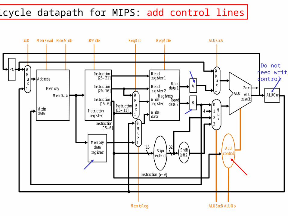
Multicycle datapath for MIPS: add control lines
Do notneed writecontrol
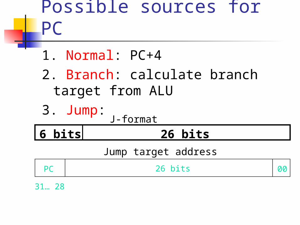
Possible sources for PC1. Normal: PC+42. Branch: calculate branch target
from ALU3. Jump:
6 bits 26 bits
PC
31… 28
26 bits 00
J-format
Jump target address
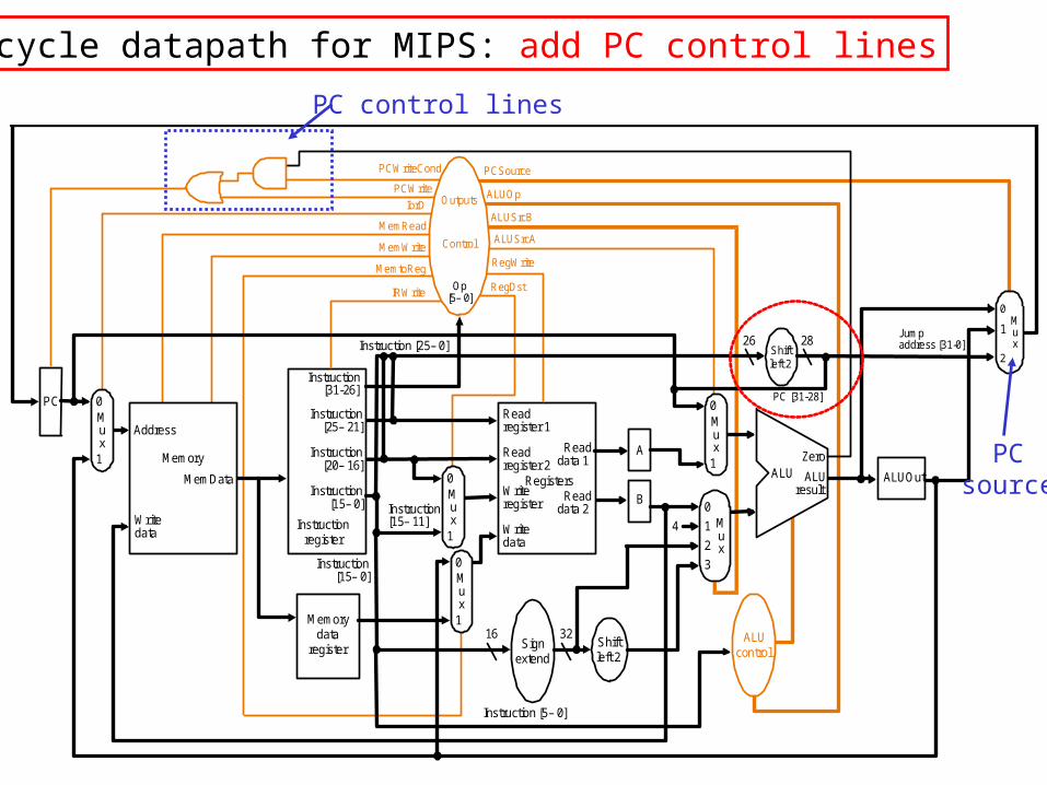
Shiftleft 2
PCMux
0
1
RegistersWriteregister
Writedata
Readdata 1
Readdata 2
Readregister 1
Readregister 2
Instruction[15– 11]
Mux
0
1
Mux
0
1
4
Instruction[15– 0]
Signextend
3216
Instruction[25– 21]
Instruction[20– 16]
Instruction[15– 0]
Instructionregister
ALUcontrol
ALUresult
ALUZero
Memorydata
register
A
B
IorD
MemRead
MemWrite
MemtoReg
PCWriteCond
PCWrite
IRWrite
ALUOp
ALUSrcB
ALUSrcA
RegDst
PCSource
RegWrite
Control
Outputs
Op[5– 0]
Instruction[31-26]
Instruction [5– 0]
Mux
0
2
Jumpaddress [31-0]Instruction [25– 0] 26 28
Shiftleft 2
PC [31-28]
1
1 Mux
0
3
2
Mux
0
1ALUOut
Memory
MemData
Writedata
Address
Multicycle datapath for MIPS: add PC control lines
PCsource
PC control lines
0 1
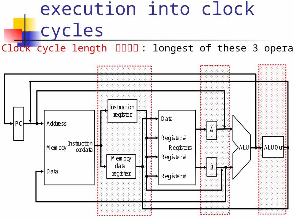
Break instruction execution into clock cycles
PC
Memory
Address
Instructionor data
Data
Instructionregister
Registers
Register #
Data
Register #
Register #
ALU
Memorydata
register
A
B
ALUOut
Clock cycle length 時脈長度 : longest of these 3 operations
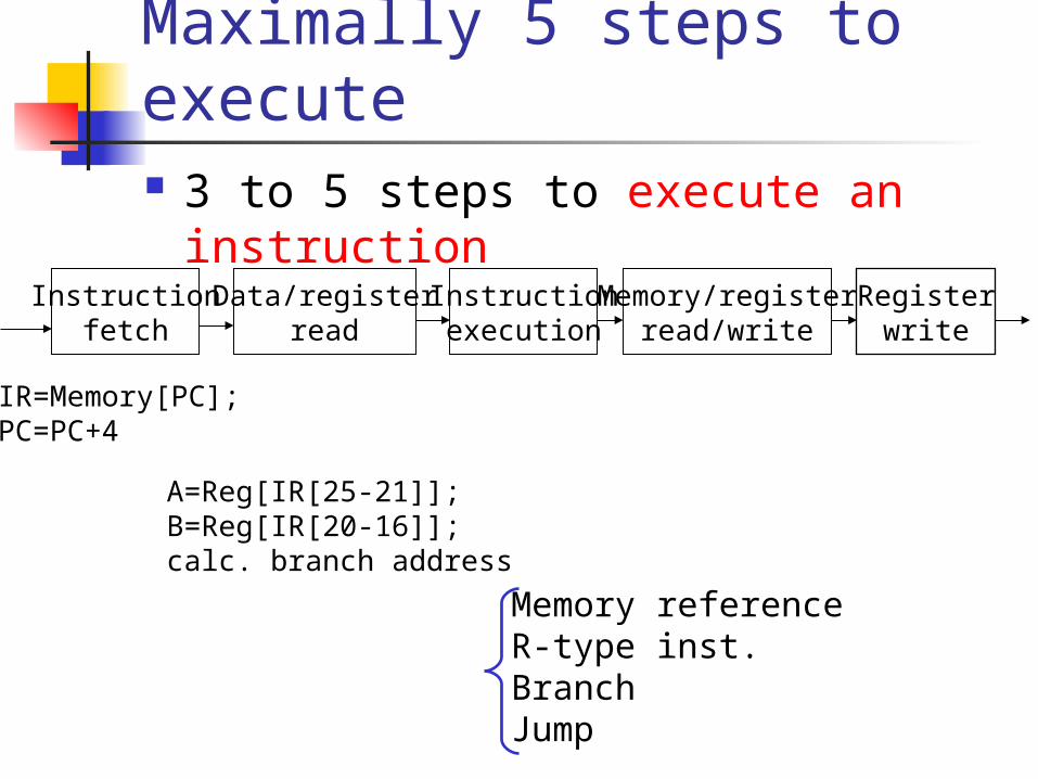
Maximally 5 steps to execute 3 to 5 steps to execute an
instructionInstruction
fetchData/register
readInstructionexecution
Memory/registerread/write
Registerwrite
IR=Memory[PC];PC=PC+4
A=Reg[IR[25-21]];B=Reg[IR[20-16]];calc. branch address
Memory referenceR-type inst.BranchJump
Shiftleft 2
PCMux
0
1
RegistersWriteregister
Writedata
Readdata 1
Readdata 2
Readregister 1
Readregister 2
Instruction[15– 11]
Mux
0
1
Mux
0
1
4
Instruction[15– 0]
Signextend
3216
Instruction[25– 21]
Instruction[20– 16]
Instruction[15– 0]
Instructionregister
ALUcontrol
ALUresult
ALUZero
Memorydata
register
A
B
IorD
MemRead
MemWrite
MemtoReg
PCWriteCond
PCWrite
IRWrite
ALUOp
ALUSrcB
ALUSrcA
RegDst
PCSource
RegWrite
Control
Outputs
Op[5– 0]
Instruction[31-26]
Instruction [5– 0]
Mux
0
2
Jumpaddress [31-0]Instruction [25– 0] 26 28
Shiftleft 2
PC [31-28]
1
1 Mux
0
3
2
Mux
0
1ALUOut
Memory
MemData
Writedata
AddressPCWrite
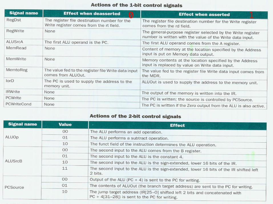
PCSource = 10
ALUSrcA = 1ALUSrcB = 00ALUOp = 01PCWriteCond
PCSource = 01
ALUSrcA =1ALUSrcB = 00ALUOp= 10
RegDst = 1RegWrite
MemtoReg = 0
MemWriteIorD = 1
MemReadIorD = 1
ALUSrcA = 1ALUSrcB = 10ALUOp = 00
RegDst = 0RegWrite
MemtoReg =1
ALUSrcA = 0ALUSrcB = 11ALUOp = 00
MemReadALUSrcA = 0
IorD = 0IRWrite
ALUSrcB = 01ALUOp = 00
PCWritePCSource = 00
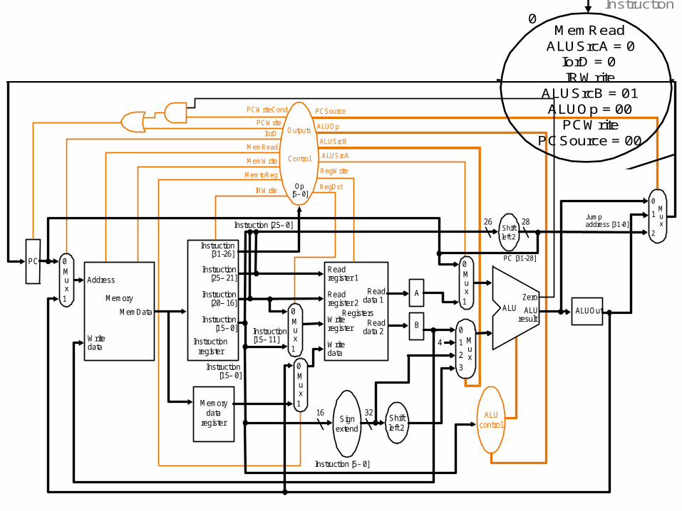
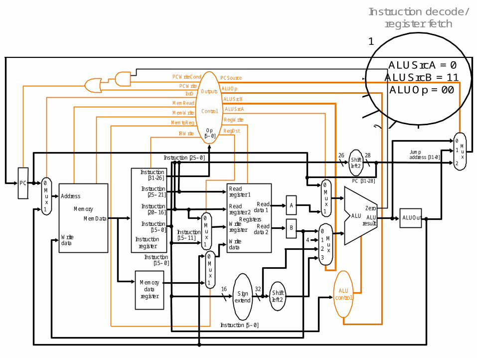
Instruction fetchInstruction decode/
register fetch
Jumpcompletion
BranchcompletionExecution
Memory addresscomputation
Memoryaccess
Memoryaccess R-type completion
Write-back step
(Op
= 'J
')
(Op =
'LW
')
4
01
9862
753
Start
Shiftleft 2
PCMux
0
1
RegistersWriteregister
Writedata
Readdata 1
Readdata 2
Readregister 1
Readregister 2
Instruction[15– 11]
Mux
0
1
Mux
0
1
4
Instruction[15– 0]
Signextend
3216
Instruction[25– 21]
Instruction[20– 16]
Instruction[15– 0]
Instructionregister
ALUcontrol
ALUresult
ALUZero
Memorydata
register
A
B
IorD
MemRead
MemWrite
MemtoReg
PCWriteCond
PCWrite
IRWrite
ALUOp
ALUSrcB
ALUSrcA
RegDst
PCSource
RegWrite
Control
Outputs
Op[5– 0]
Instruction[31-26]
Instruction [5– 0]
Mux
0
2
Jumpaddress [31-0]Instruction [25– 0] 26 28
Shiftleft 2
PC [31-28]
1
1 Mux
0
3
2
Mux
0
1ALUOut
Memory
MemData
Writedata
Address
PCWritePCSource = 10
ALUSrcA = 1ALUSrcB = 00ALUOp = 01PCWriteCond
PCSource = 01
ALUSrcA =1ALUSrcB = 00ALUOp= 10
RegDst = 1RegWrite
MemtoReg = 0
MemWriteIorD = 1
MemReadIorD = 1
ALUSrcA = 1ALUSrcB = 10ALUOp = 00
RegDst = 0RegWrite
MemtoReg =1
ALUSrcA = 0ALUSrcB = 11ALUOp = 00
MemReadALUSrcA = 0
IorD = 0IRWrite
ALUSrcB = 01ALUOp = 00
PCWritePCSource = 00
Instruction fetchInstruction decode/
register fetch
Jumpcompletion
BranchcompletionExecution
Memory addresscomputation
Memoryaccess
Memoryaccess R-type completion
Write-back step
(Op
= 'J
')
(Op =
'LW
')
4
01
9862
753
Start
Example: Memory reference (load)
Shiftleft 2
MemtoReg
IorD MemRead MemWrite
PC
Memory
MemData
Writedata
Mux
0
1
RegistersWriteregister
Writedata
Readdata 1
Readdata 2
Readregister 1
Readregister 2
Instruction[15– 11]
Mux
0
1
Mux
0
1
4
ALUOpALUSrcB
RegDst RegWrite
Instruction[15– 0]
Instruction [5– 0]
Signextend
3216
Instruction[25– 21]
Instruction[20– 16]
Instruction[15– 0]
Instructionregister
1 Mux
0
3
2
ALUcontrol
Mux
0
1ALU
resultALU
ALUSrcA
ZeroA
B
ALUOut
IRWrite
Address
Memorydata
register
lw $t1, offset($t2)
3. ALUout=A+sign(IR[15-0]); ALUSrcA=1,ALUSrcB=10
4. MDR = Memory[ALUout]; IorD=1, MemRead=1,
5. Reg[IR[20-16]]=MDR; RegWrite=1, RegDst=0, MemtoReg=1
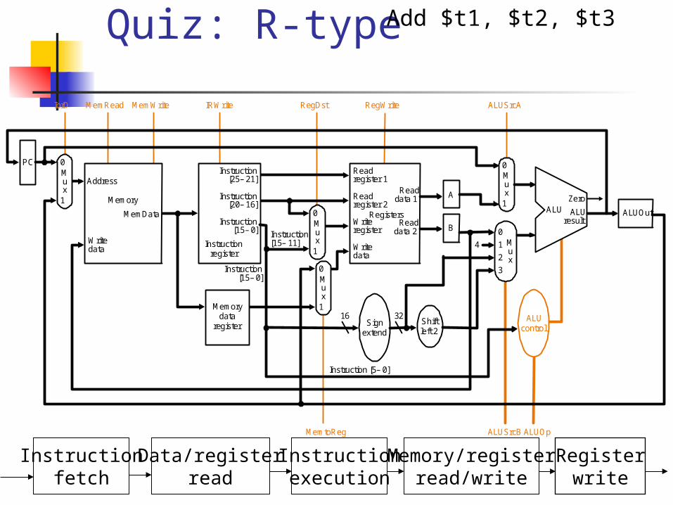
Quiz: R-type
Shiftleft 2
MemtoReg
IorD MemRead MemWrite
PC
Memory
MemData
Writedata
Mux
0
1
RegistersWriteregister
Writedata
Readdata 1
Readdata 2
Readregister 1
Readregister 2
Instruction[15– 11]
Mux
0
1
Mux
0
1
4
ALUOpALUSrcB
RegDst RegWrite
Instruction[15– 0]
Instruction [5– 0]
Signextend
3216
Instruction[25– 21]
Instruction[20– 16]
Instruction[15– 0]
Instructionregister
1 Mux
0
3
2
ALUcontrol
Mux
0
1ALU
resultALU
ALUSrcA
ZeroA
B
ALUOut
IRWrite
Address
Memorydata
register
Add $t1, $t2, $t3
Instructionfetch
Data/registerread
Instructionexecution
Memory/registerread/write
Registerwrite
Control for multicycle datapath
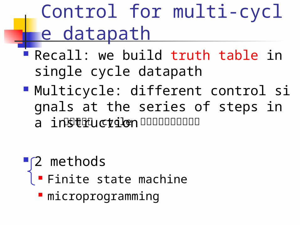
Control for multi-cycle datapath
Recall: we build truth table in single cycle datapath
Multicycle: different control signals at the series of steps in a instruction
2 methods Finite state machine microprogramming
指令中每個 cycle 都需要不同的控制訊號
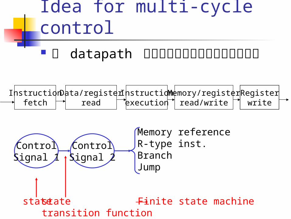
Idea for multi-cycle control 在 datapath 中每個階段都需要不同的
控制訊號Instruction
fetchData/register
readInstructionexecution
Memory/registerread/write
Registerwrite
ControlSignal 1
ControlSignal 2
Memory referenceR-type inst.BranchJump
state statetransition function
Finite state machine
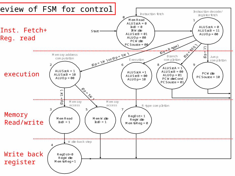
PCWritePCSource = 10
ALUSrcA = 1ALUSrcB = 00ALUOp = 01PCWriteCond
PCSource = 01
ALUSrcA =1ALUSrcB = 00ALUOp= 10
RegDst = 1RegWrite
MemtoReg = 0
MemWriteIorD = 1
MemReadIorD = 1
ALUSrcA = 1ALUSrcB = 10ALUOp = 00
RegDst = 0RegWrite
MemtoReg =1
ALUSrcA = 0ALUSrcB = 11ALUOp = 00
MemReadALUSrcA = 0
IorD = 0IRWrite
ALUSrcB = 01ALUOp = 00
PCWritePCSource = 00
Instruction fetchInstruction decode/
register fetch
Jumpcompletion
BranchcompletionExecution
Memory addresscomputation
Memoryaccess
Memoryaccess R-type completion
Write-back step
(Op
= 'J
')
(Op =
'LW
')
4
01
9862
753
Start
Preview of FSM for control
Inst. Fetch+Reg. read
execution
MemoryRead/write
Write backregister
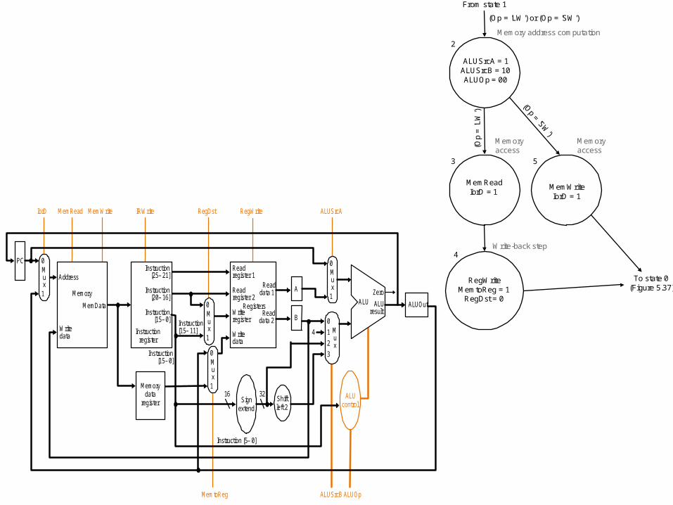
MemWriteIorD = 1
MemReadIorD = 1
ALUSrcA = 1ALUSrcB = 10ALUOp = 00
RegWriteMemtoReg = 1
RegDst = 0
Memory address computation
(Op = 'LW') or (Op = 'SW')
Memoryaccess
Write-back step
(Op = 'SW
')
(Op
= 'L
W')
4
2
53
From state 1
To state 0(Figure 5.37)
Memoryaccess
Shiftleft 2
MemtoReg
IorD MemRead MemWrite
PC
Memory
MemData
Writedata
Mux
0
1
RegistersWriteregister
Writedata
Readdata 1
Readdata 2
Readregister 1
Readregister 2
Instruction[15– 11]
Mux
0
1
Mux
0
1
4
ALUOpALUSrcB
RegDst RegWrite
Instruction[15– 0]
Instruction [5– 0]
Signextend
3216
Instruction[25– 21]
Instruction[20– 16]
Instruction[15– 0]
Instructionregister
1 Mux
0
3
2
ALUcontrol
Mux
0
1ALU
resultALU
ALUSrcA
ZeroA
B
ALUOut
IRWrite
Address
Memorydata
register
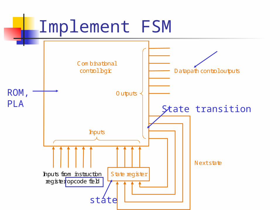
Implement FSM
Datapath control outputs
State registerInputs from instructionregister opcode field
Outputs
Combinationalcontrol logic
Inputs
Next state
State transition
ROM,PLA
state
Control for multicycle datapath
Microprogramming
Motivation If there are over 100 instructions,
the graphical representation of FSM is impossible…大指令集,要畫出 FSM 的狀態轉移圖很難
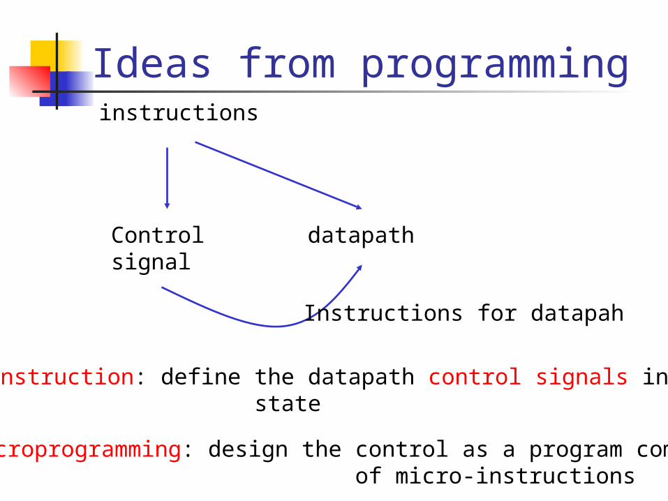
Ideas from programminginstructions
datapathControlsignal
Instructions for datapah
microinstruction: define the datapath control signals in a given state
microprogramming: design the control as a program composed of micro-instructions
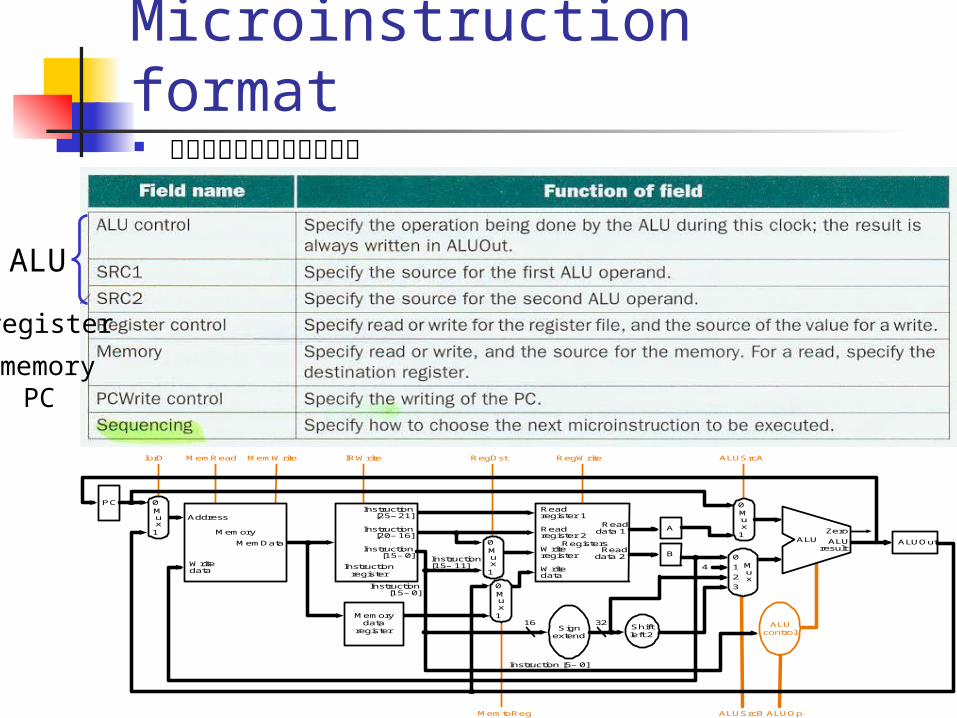
Microinstruction format 依所控制的功能單元分欄位
ALU
register
memoryPC
Shiftleft 2
MemtoReg
IorD MemRead MemWrite
PC
Memory
MemData
Writedata
Mux
0
1
RegistersWriteregister
Writedata
Readdata 1
Readdata 2
Readregister 1
Readregister 2
Instruction[15– 11]
Mux
0
1
Mux
0
1
4
ALUOpALUSrcB
RegDst RegWrite
Instruction[15– 0]
Instruction [5– 0]
Signextend
3216
Instruction[25– 21]
Instruction[20– 16]
Instruction[15– 0]
Instructionregister
1 Mux
0
3
2
ALUcontrol
Mux
0
1ALU
resultALU
ALUSrcA
ZeroA
B
ALUOut
IRWrite
Address
Memorydata
register
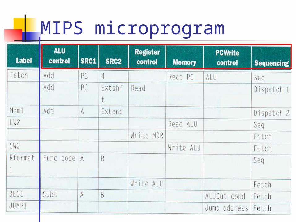
MIPS microprogram
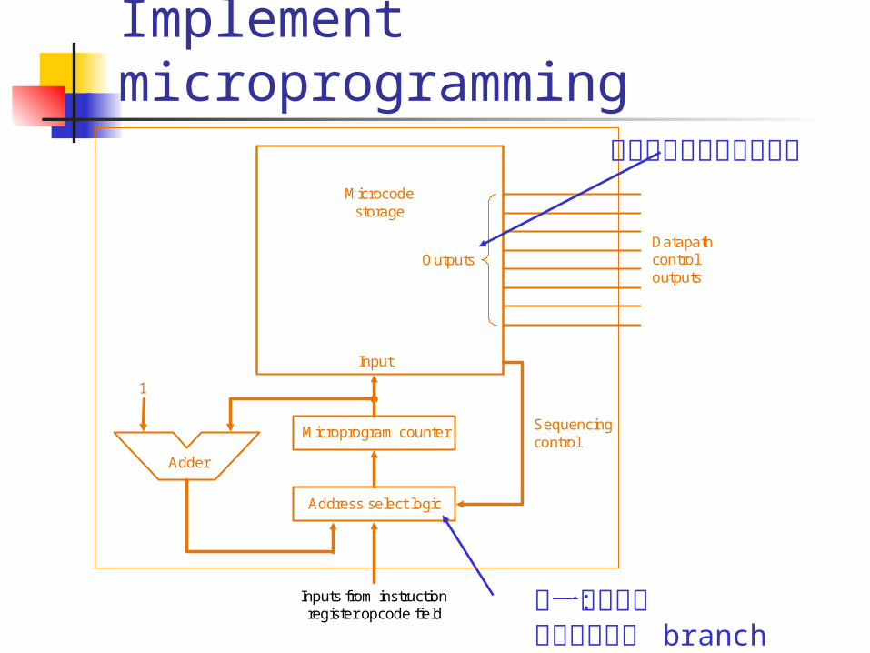
Implement microprogramming
Microprogram counter
Address select logic
Adder
1
Input
Datapathcontroloutputs
Microcodestorage
Inputs from instructionregister opcode field
Outputs
Sequencingcontrol
下一個指令:循序執行或有 branch
微指令對應到的控制訊號