Embed Size (px)
Citation preview
Advanced Robotics, Vol. 20, No. 11, pp. 1281–1301 (2006) VSP and Robotics Society of Japan 2006.Also available online - www.brill.nl/ar
Full paper
Nano encoders based on vertical arrays of individualcarbon nanotubes
LIXIN DONG 1, ARUNKUMAR SUBRAMANIAN 1,DANIEL HUGENTOBLER 1, BRADLEY J. NELSON 1,∗ and YU SUN 2
1 Institute of Robotics and Intelligent Systems, ETH Zurich, 8092, Zurich, Switzerland2 Department of Mechanical and Industrial Engineering, University of Toronto, Toronto, Canada
Received 27 April 2006; accepted 9 July 2006
Abstract—Linear encoders for nanoscale position sensing based on vertical arrays of individualcarbon nanotubes are presented. Vertical arrays of single multi-walled carbon nanotubes (MWNTs)are realized using a combination of electron beam lithography (EBL) and plasma-enhanced chemicalvapour deposition growth. EBL is used to define 50- to 150-nm nickel catalyst dots at preciselocations on a silicon chip. Precise control of the position, density and alignment of the tubes has beenachieved. Aligned nanotube arrays with spacing varying from 250 nm to 25 µm are realized. Fieldemission properties of the array are investigated inside a scanning electron microscope equipped witha 3-d.o.f. nanorobotic manipulator with nanometer resolution functioning as a scanning anode. Withthis scanning anode and the single MWNT array, a nano encoder is investigated experimentally.Vertical position is detected by the change in emission current, whereas the horizontal position ofthe scanning anode is sensed from the emission distribution. A resolution of 98.3 nm in the verticaldirection and 38.0 nm (best: 12.9 nm) in the lateral direction has been achieved.
Keywords: Carbon nanotube array; field emission; nano encoder; nanorobotic manipulator; scanninganode.
1. INTRODUCTION
In electric servomotors, encoders play a significant role by providing precisionangular or linear position sensing feedback. Similarly, with the development of nanomachines [1–4] nanometer-scale position sensing with nanometer-sized devices isrequired for their successful application.
To shrink the sizes of conventional optical encoders, different measurementprinciples must be considered. Although tunneling current and laser-deflectiontechniques can provide extremely high resolution [5, 6], the effective distance of
∗To whom correspondence should be addressed. E-mail: [email protected]
1282 L. Dong et al.
the former is less than 1 nm and the latter generally involves a complex laserapparatus. Another possible feedback mechanism is to use the interlayer resistanceof a telescoping multi-walled carbon nanotube (MWNT) for position sensing [7].The potential for quantized interlayer conductance can result in resolutions atatomic lattice levels [8]. On the other hand, the dependence of field emissioncurrents on inter-electrode distance has shown promise for non-contact positionsensing [9, 10]. Recent results with individual nanotube emitters and telescopingnanotubes have shown the feasibility of this method [11, 12]. Moreover, the energydistribution around a field emitter [13, 14] is a potential technique for lateral positionsensing.
Plasma-enhanced chemical vapour deposition (PECVD) has been successfullyused for the growth of individual MWNTs from nickel catalyst nanodots definedby electron beam lithography (EBL) [13]. In this paper, we present a nano encoderbased on vertically-aligned single MWNT emitters grown with this technique.Vertical and lateral position sensing are investigated from experimental, theoreticaland design perspectives.
In the following, directed growth of single MWNT arrays is introduced inSection 2. The design and operating principle of nano encoders is presented inSection 3. A nanomanipulation-based scanning anode technique for field emissionproperty characterization is shown in Section 4 and the basic field emission propertyof an individual tube in the array is measured. In Section 5, experiments with singleMWNT array-based linear nano encoders are described.
2. DIRECTED GROWTH OF SINGLE MWNT ARRAYS
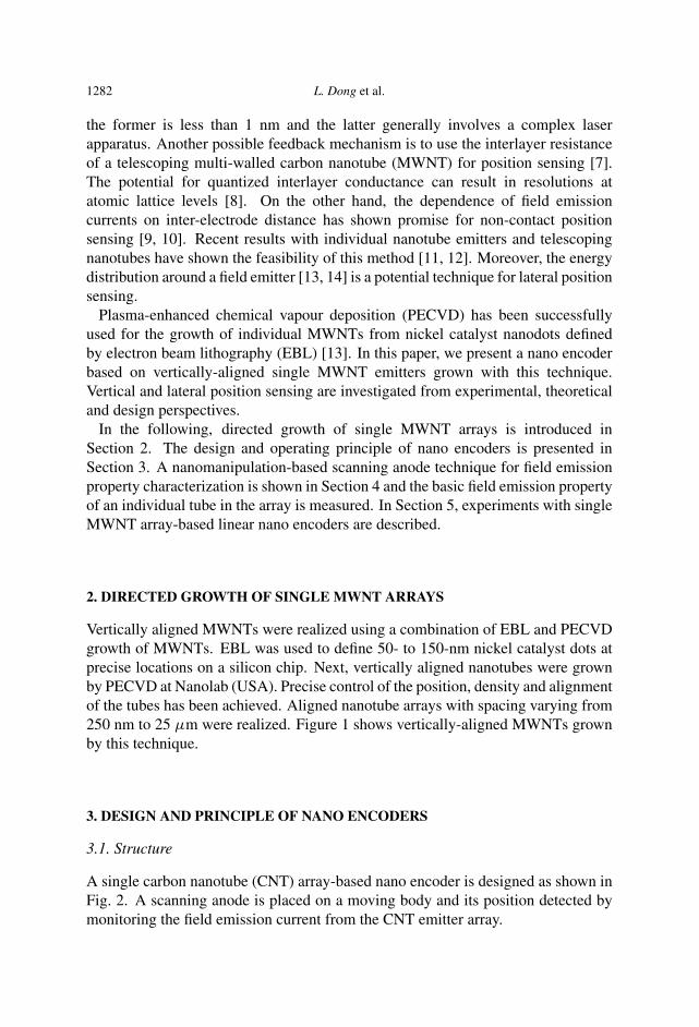
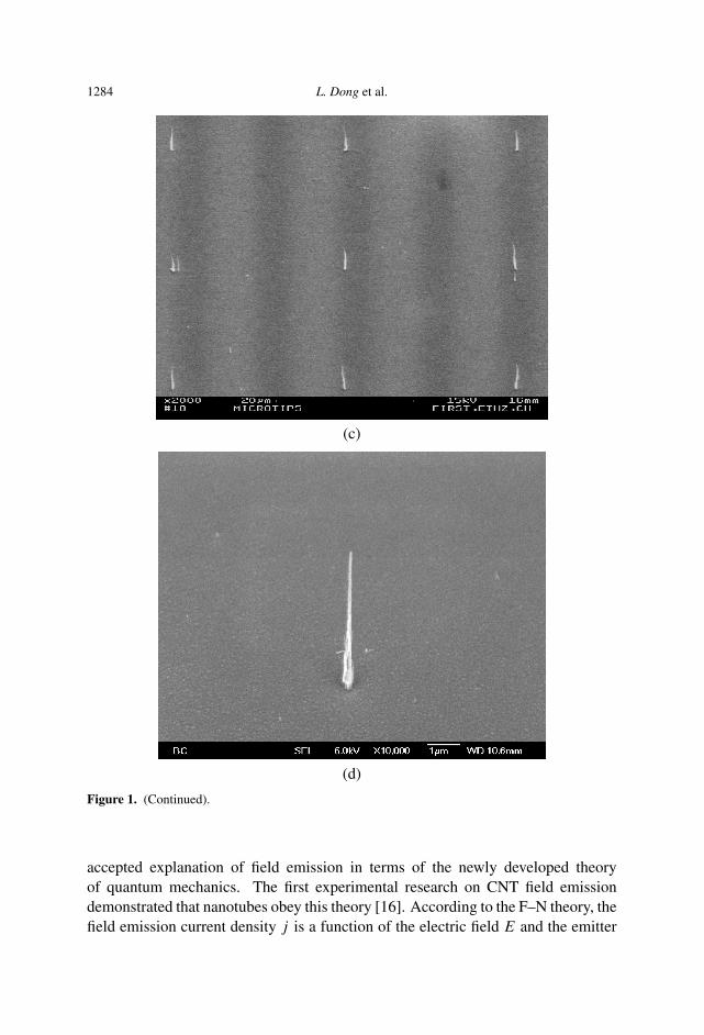
Vertically aligned MWNTs were realized using a combination of EBL and PECVDgrowth of MWNTs. EBL was used to define 50- to 150-nm nickel catalyst dots atprecise locations on a silicon chip. Next, vertically aligned nanotubes were grownby PECVD at Nanolab (USA). Precise control of the position, density and alignmentof the tubes has been achieved. Aligned nanotube arrays with spacing varying from250 nm to 25 µm were realized. Figure 1 shows vertically-aligned MWNTs grownby this technique.
3. DESIGN AND PRINCIPLE OF NANO ENCODERS
3.1. Structure
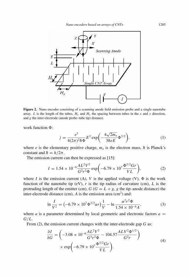
A single carbon nanotube (CNT) array-based nano encoder is designed as shown inFig. 2. A scanning anode is placed on a moving body and its position detected bymonitoring the field emission current from the CNT emitter array.
Nano encoders based on arrays of CNTs 1283
(a)
(b)
Figure 1. Single MWNT arrays: (a) 250-nm to 1-µm spacing (insets show logos ‘IRIS’ and ‘ETHZ’in pseudo-colors observed at a 45◦ tilt angle), (b) 10-µm spacing 3 × 4 array of single MWNTs,(c) 25-µm spacing 3 × 3 array of single MWNTs and (d) an individual tube in the array. (Scale bars:10 µm.)
3.2. Vertical position sensing
Field emission from a nanotube emitter is governed by the Fowler–Nordheim(F–N) theory [15]. This theory, originally published in 1928, was the first generally
1284 L. Dong et al.
(c)
(d)
Figure 1. (Continued).
accepted explanation of field emission in terms of the newly developed theoryof quantum mechanics. The first experimental research on CNT field emissiondemonstrated that nanotubes obey this theory [16]. According to the F–N theory, thefield emission current density j is a function of the electric field E and the emitter
Nano encoders based on arrays of CNTs 1285
Figure 2. Nano encoder consisting of a scanning anode field emission probe and a single nanotubearray. L is the length of the tubes, Hx and Hy the spacing between tubes in the x and y direction,and g the inter-electrode (anode probe–tube tip) distance.
work function �:
j = e3
4(2π)2h̄�E2 exp
(−4
√2me
3h̄eE�3/2
), (1)
where e is the elementary positive charge, me is the electron mass, h̄ is Planck’sconstant and h̄ = h/2π .
The emission current can then be expressed as [15]:
I = 1.54 × 10⁻⁶ AL2V 2
G2r2�exp
(−6.79 × 10⁷ �3/2Gr
V L
), (2)
where I is the emission current (A), V is the applied voltage (V), � is the workfunction of the nanotube tip (eV), r is the tip radius of curvature (cm), L is theprotruding length of the emitter (cm), G (G = L + g, g the tip–anode distance) theinter-electrode distance (cm), A is the emission area (cm2) and:
lnI
V 2= (−6.79 × 10⁷�3/2αr
) 1
V− ln
α2r2�
1.54 × 10⁻⁶A, (3)
where a is a parameter determined by local geometric and electronic factors a =G/L.
From (2), the emission current changes with the inter-electrode gap G as:
∂I
∂G=
(−3.08 × 10⁻⁶ AL2V 2
G3r2�− 104.57
ALV 2�1/2
G2r
)
× exp
(−6.79 × 10⁷ �3/2Gr
V L
).
(4)
1286 L. Dong et al.
(a)
(b)
(c)
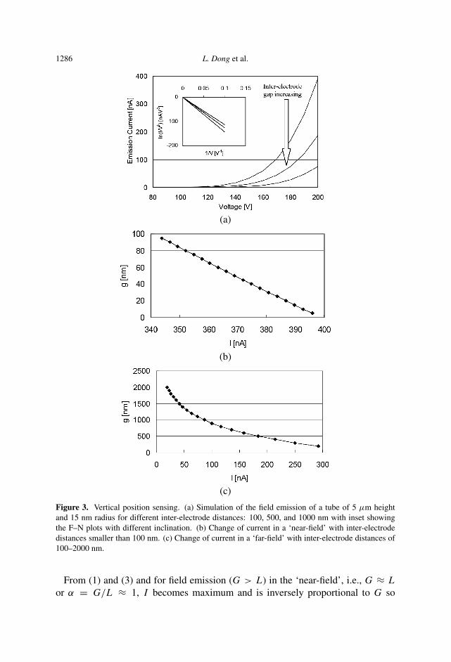
Figure 3. Vertical position sensing. (a) Simulation of the field emission of a tube of 5 µm heightand 15 nm radius for different inter-electrode distances: 100, 500, and 1000 nm with inset showingthe F–N plots with different inclination. (b) Change of current in a ‘near-field’ with inter-electrodedistances smaller than 100 nm. (c) Change of current in a ‘far-field’ with inter-electrode distances of100–2000 nm.
From (1) and (3) and for field emission (G > L) in the ‘near-field’, i.e., G ≈ L
or α = G/L ≈ 1, I becomes maximum and is inversely proportional to G so
Nano encoders based on arrays of CNTs 1287
(a)
(b)
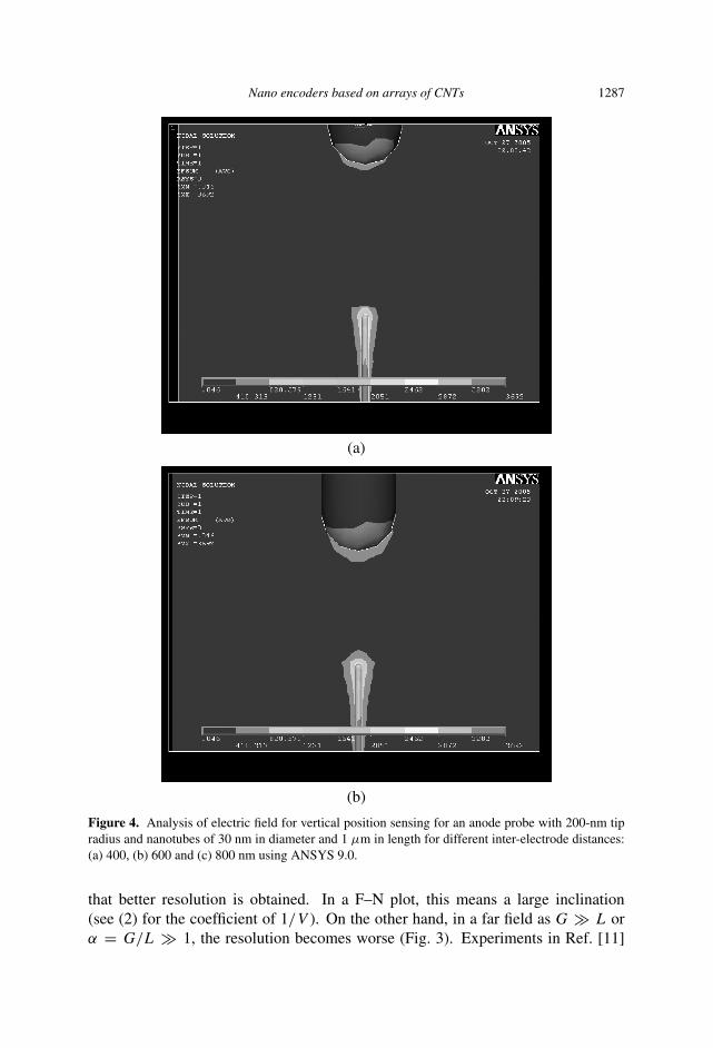
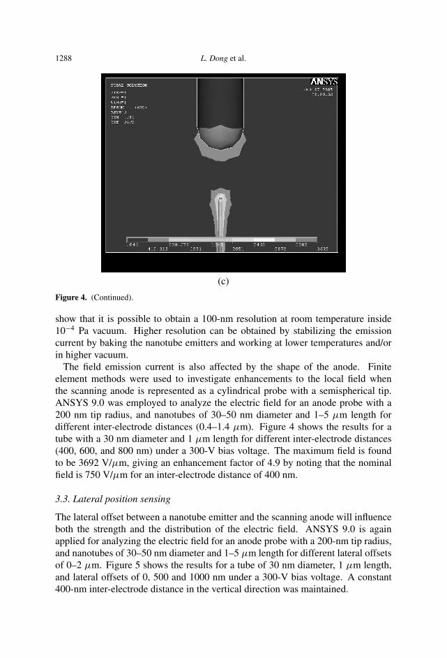
Figure 4. Analysis of electric field for vertical position sensing for an anode probe with 200-nm tipradius and nanotubes of 30 nm in diameter and 1 µm in length for different inter-electrode distances:(a) 400, (b) 600 and (c) 800 nm using ANSYS 9.0.
that better resolution is obtained. In a F–N plot, this means a large inclination(see (2) for the coefficient of 1/V ). On the other hand, in a far field as G � L orα = G/L � 1, the resolution becomes worse (Fig. 3). Experiments in Ref. [11]
1288 L. Dong et al.
(c)
Figure 4. (Continued).
show that it is possible to obtain a 100-nm resolution at room temperature inside10−4 Pa vacuum. Higher resolution can be obtained by stabilizing the emissioncurrent by baking the nanotube emitters and working at lower temperatures and/orin higher vacuum.
The field emission current is also affected by the shape of the anode. Finiteelement methods were used to investigate enhancements to the local field whenthe scanning anode is represented as a cylindrical probe with a semispherical tip.ANSYS 9.0 was employed to analyze the electric field for an anode probe with a200 nm tip radius, and nanotubes of 30–50 nm diameter and 1–5 µm length fordifferent inter-electrode distances (0.4–1.4 µm). Figure 4 shows the results for atube with a 30 nm diameter and 1 µm length for different inter-electrode distances(400, 600, and 800 nm) under a 300-V bias voltage. The maximum field is foundto be 3692 V/µm, giving an enhancement factor of 4.9 by noting that the nominalfield is 750 V/µm for an inter-electrode distance of 400 nm.
3.3. Lateral position sensing
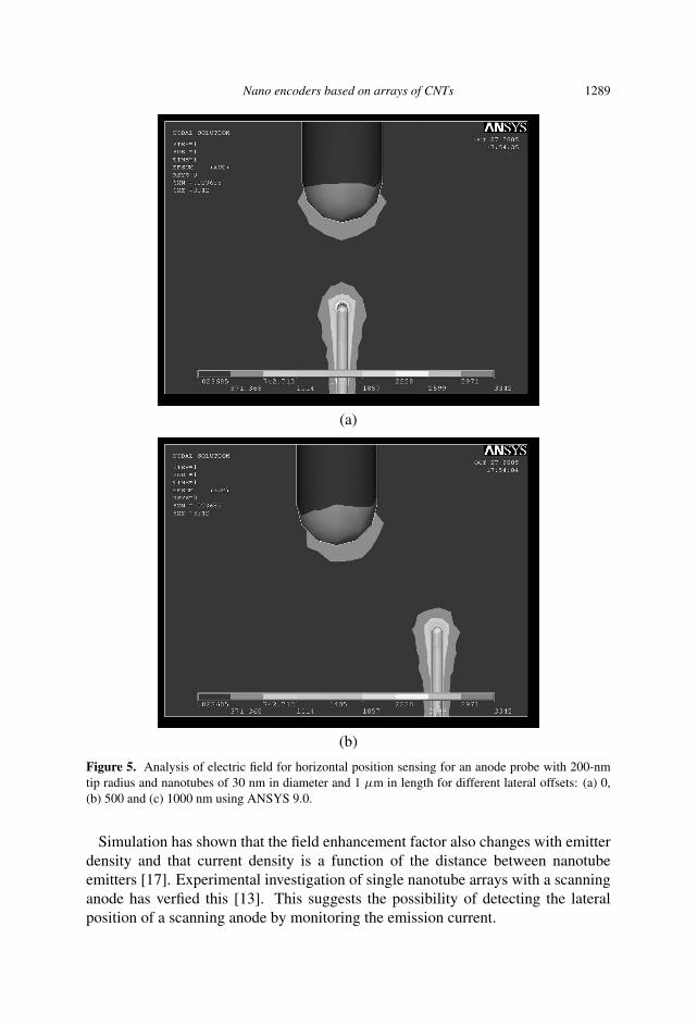
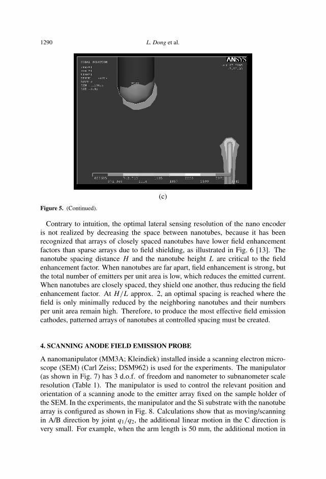
The lateral offset between a nanotube emitter and the scanning anode will influenceboth the strength and the distribution of the electric field. ANSYS 9.0 is againapplied for analyzing the electric field for an anode probe with a 200-nm tip radius,and nanotubes of 30–50 nm diameter and 1–5 µm length for different lateral offsetsof 0–2 µm. Figure 5 shows the results for a tube of 30 nm diameter, 1 µm length,and lateral offsets of 0, 500 and 1000 nm under a 300-V bias voltage. A constant400-nm inter-electrode distance in the vertical direction was maintained.
Nano encoders based on arrays of CNTs 1289
(a)
(b)
Figure 5. Analysis of electric field for horizontal position sensing for an anode probe with 200-nmtip radius and nanotubes of 30 nm in diameter and 1 µm in length for different lateral offsets: (a) 0,(b) 500 and (c) 1000 nm using ANSYS 9.0.
Simulation has shown that the field enhancement factor also changes with emitterdensity and that current density is a function of the distance between nanotubeemitters [17]. Experimental investigation of single nanotube arrays with a scanninganode has verfied this [13]. This suggests the possibility of detecting the lateralposition of a scanning anode by monitoring the emission current.
1290 L. Dong et al.
(c)
Figure 5. (Continued).
Contrary to intuition, the optimal lateral sensing resolution of the nano encoderis not realized by decreasing the space between nanotubes, because it has beenrecognized that arrays of closely spaced nanotubes have lower field enhancementfactors than sparse arrays due to field shielding, as illustrated in Fig. 6 [13]. Thenanotube spacing distance H and the nanotube height L are critical to the fieldenhancement factor. When nanotubes are far apart, field enhancement is strong, butthe total number of emitters per unit area is low, which reduces the emitted current.When nanotubes are closely spaced, they shield one another, thus reducing the fieldenhancement factor. At H/L approx. 2, an optimal spacing is reached where thefield is only minimally reduced by the neighboring nanotubes and their numbersper unit area remain high. Therefore, to produce the most effective field emissioncathodes, patterned arrays of nanotubes at controlled spacing must be created.
4. SCANNING ANODE FIELD EMISSION PROBE
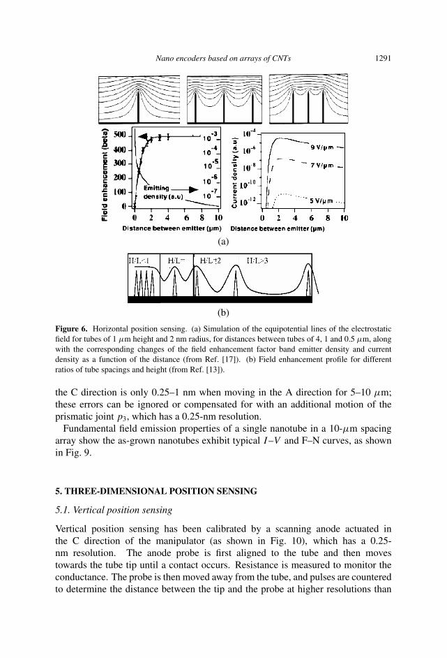
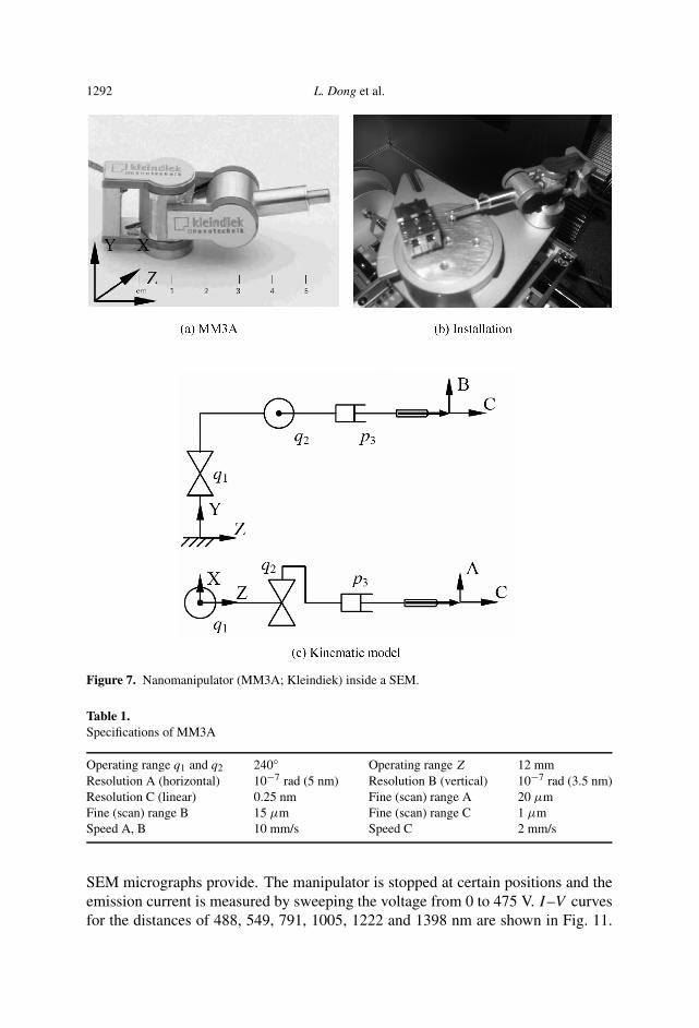
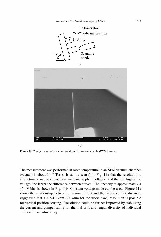
A nanomanipulator (MM3A; Kleindiek) installed inside a scanning electron micro-scope (SEM) (Carl Zeiss; DSM962) is used for the experiments. The manipulator(as shown in Fig. 7) has 3 d.o.f. of freedom and nanometer to subnanometer scaleresolution (Table 1). The manipulator is used to control the relevant position andorientation of a scanning anode to the emitter array fixed on the sample holder ofthe SEM. In the experiments, the manipulator and the Si substrate with the nanotubearray is configured as shown in Fig. 8. Calculations show that as moving/scanningin A/B direction by joint q1/q2, the additional linear motion in the C direction isvery small. For example, when the arm length is 50 mm, the additional motion in
Nano encoders based on arrays of CNTs 1291
(a)
(b)
Figure 6. Horizontal position sensing. (a) Simulation of the equipotential lines of the electrostaticfield for tubes of 1 µm height and 2 nm radius, for distances between tubes of 4, 1 and 0.5 µm, alongwith the corresponding changes of the field enhancement factor band emitter density and currentdensity as a function of the distance (from Ref. [17]). (b) Field enhancement profile for differentratios of tube spacings and height (from Ref. [13]).
the C direction is only 0.25–1 nm when moving in the A direction for 5–10 µm;these errors can be ignored or compensated for with an additional motion of theprismatic joint p3, which has a 0.25-nm resolution.
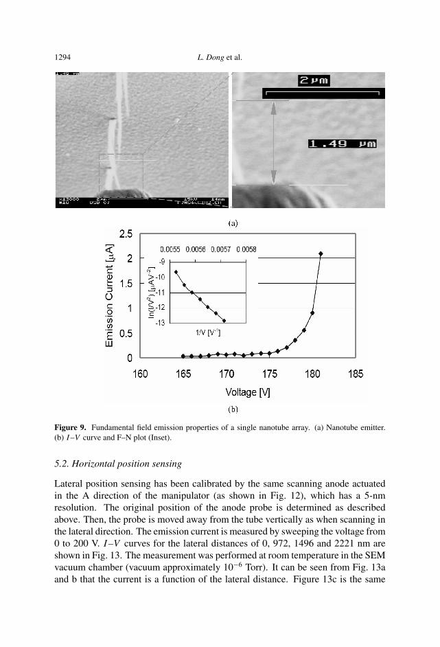
Fundamental field emission properties of a single nanotube in a 10-µm spacingarray show the as-grown nanotubes exhibit typical I–V and F–N curves, as shownin Fig. 9.
5. THREE-DIMENSIONAL POSITION SENSING
5.1. Vertical position sensing
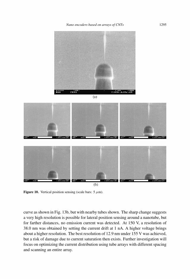
Vertical position sensing has been calibrated by a scanning anode actuated inthe C direction of the manipulator (as shown in Fig. 10), which has a 0.25-nm resolution. The anode probe is first aligned to the tube and then movestowards the tube tip until a contact occurs. Resistance is measured to monitor theconductance. The probe is then moved away from the tube, and pulses are counteredto determine the distance between the tip and the probe at higher resolutions than
1292 L. Dong et al.
Figure 7. Nanomanipulator (MM3A; Kleindiek) inside a SEM.
Table 1.Specifications of MM3A
Operating range q1 and q2 240◦ Operating range Z 12 mmResolution A (horizontal) 10−7 rad (5 nm) Resolution B (vertical) 10−7 rad (3.5 nm)Resolution C (linear) 0.25 nm Fine (scan) range A 20 µmFine (scan) range B 15 µm Fine (scan) range C 1 µmSpeed A, B 10 mm/s Speed C 2 mm/s
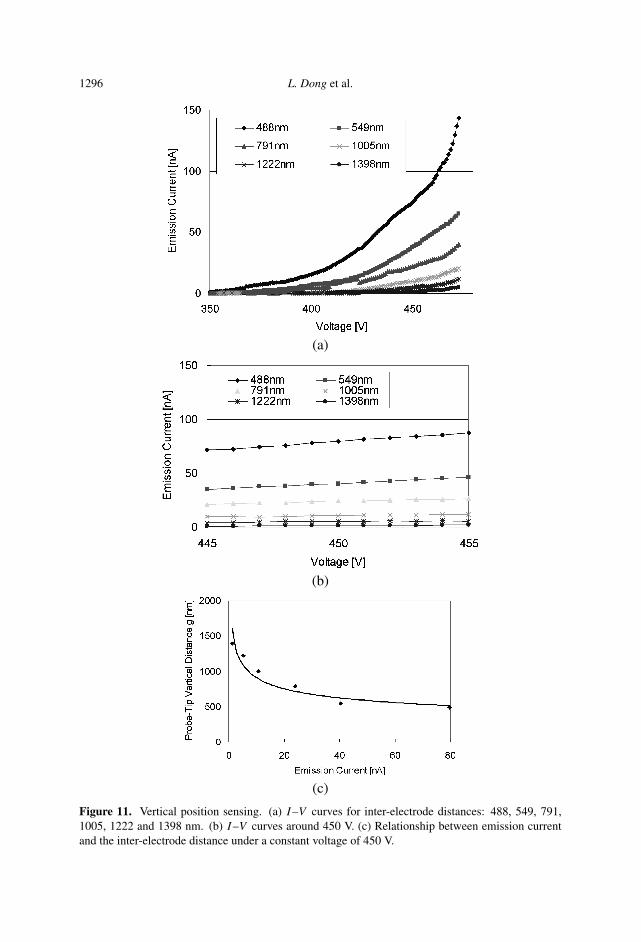
SEM micrographs provide. The manipulator is stopped at certain positions and theemission current is measured by sweeping the voltage from 0 to 475 V. I–V curvesfor the distances of 488, 549, 791, 1005, 1222 and 1398 nm are shown in Fig. 11.
Nano encoders based on arrays of CNTs 1293
(a)
(b)
Figure 8. Configuration of scanning anode and Si substrate with MWNT array.
The measurement was performed at room temperature in an SEM vacuum chamber(vacuum is about 10−6 Torr). It can be seen from Fig. 11a that the resolution isa function of inter-electrode distance and applied voltages, and that the higher thevoltage, the larger the difference between curves. The linearity at approximately a450-V bias is shown in Fig. 11b. Constant voltage mode can be used. Figure 11cshows the relationship between emission current and the inter-electrode distance,suggesting that a sub-100-nm (98.3-nm for the worst case) resolution is possiblefor vertical position sensing. Rresolution could be further improved by stabilizingthe current and compensating for thermal drift and length diversity of individualemitters in an entire array.
1294 L. Dong et al.
Figure 9. Fundamental field emission properties of a single nanotube array. (a) Nanotube emitter.(b) I–V curve and F–N plot (Inset).
5.2. Horizontal position sensing
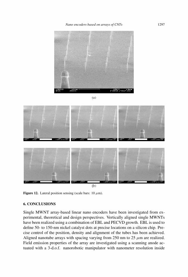
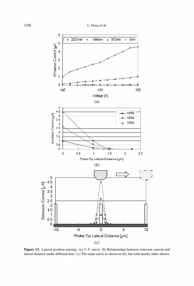
Lateral position sensing has been calibrated by the same scanning anode actuatedin the A direction of the manipulator (as shown in Fig. 12), which has a 5-nmresolution. The original position of the anode probe is determined as describedabove. Then, the probe is moved away from the tube vertically as when scanning inthe lateral direction. The emission current is measured by sweeping the voltage from0 to 200 V. I–V curves for the lateral distances of 0, 972, 1496 and 2221 nm areshown in Fig. 13. The measurement was performed at room temperature in the SEMvacuum chamber (vacuum approximately 10−6 Torr). It can be seen from Fig. 13aand b that the current is a function of the lateral distance. Figure 13c is the same
Nano encoders based on arrays of CNTs 1295
Figure 10. Vertical position sensing (scale bars: 5 µm).
curve as shown in Fig. 13b, but with nearby tubes shown. The sharp change suggestsa very high resolution is possible for lateral position sensing around a nanotube, butfor farther distances, no emission current was detected. At 150 V, a resolution of38.0 nm was obtained by setting the current drift at 1 nA. A higher voltage bringsabout a higher resolution. The best resolution of 12.9 nm under 155 V was achieved,but a risk of damage due to current saturation then exists. Further investigation willfocus on optimizing the current distribution using tube arrays with different spacingand scanning an entire array.
1296 L. Dong et al.
(a)
(b)
(c)
Figure 11. Vertical position sensing. (a) I–V curves for inter-electrode distances: 488, 549, 791,1005, 1222 and 1398 nm. (b) I–V curves around 450 V. (c) Relationship between emission currentand the inter-electrode distance under a constant voltage of 450 V.
Nano encoders based on arrays of CNTs 1297
Figure 12. Lateral position sensing (scale bars: 10 µm).
6. CONCLUSIONS
Single MWNT array-based linear nano encoders have been investigated from ex-perimental, theoretical and design perspectives. Vertically aligned single MWNTshave been realized using a combination of EBL and PECVD growth. EBL is used todefine 50- to 150-nm nickel catalyst dots at precise locations on a silicon chip. Pre-cise control of the position, density and alignment of the tubes has been achieved.Aligned nanotube arrays with spacing varying from 250 nm to 25 µm are realized.Field emission properties of the array are investigated using a scanning anode ac-tuated with a 3-d.o.f. nanorobotic manipulator with nanometer resolution inside
1298 L. Dong et al.
(a)
(b)
(c)
Figure 13. Lateral position sensing. (a) I–V curve. (b) Relationship between emission current andlateral distance under different bias. (c) The same curve as shown in (b), but with nearby tubes shown.
Nano encoders based on arrays of CNTs 1299
a SEM. Vertical and lateral positions have been detected by monitoring the emis-sion current change. A resolution of 98.3 nm in the vertical direction and 38.0 nm(best: 12.9 nm) in the lateral direction has been achieved.
REFERENCES
1. V. Balzani, M. Venturi and A. Credi, Molecular Devices and Machines: A Journey into theNanoworld. Wiley-VCH, Weinheim (2003).
2. K. E. Drexler, Nanosystems: Molecular Machinery, Manufacturing, & Computation. Wiley, NewYork (1992).
3. A. M. Fennimore, T. D. Yuzvinsky, W.-Q. Han, M. S. Fuhrer, J. Cumings and A. Zettl, Rotationalactuators based on carbon nano-tubes, Nature 424, 408–410 (2003).
4. L. X. Dong, B. J. Nelson, T. Fukuda and F. Arai, Towards linear nano servomotors with integratedposition sensing, in: Proc. IEEE Int. Conf. on Robotics & Automation, Barcelona, pp. 867–872(2005).
5. G. Binnig, H. Rohrer, C. Gerber and E. Weibel, Surface studies by scanning tunnelingmicroscopy, Phys. Rev. Lett. 49, 57–61 (1982).
6. G. Binnig, C. F. Quate and C. Gerber, Atomic force microscope, Phys. Rev. Lett. 56, 93–96(1986).
7. P. Liu, L. X. Dong, T. Fukuda, F. Arai, M. Nagai and Y. Imaizumi, Carbon nanotubes basedposition sensors, in: Proc. Int. Conf. on Intelligent Mechatronics and Automation, Chengdu,pp. 12–17 (2004).
8. A. Hansson and S. Stafstro, Intershell conductance in multiwall carbon nanotubes, Phys. Rev. B67 (2003).
9. W. Zhu, C. Bower, O. Zhou, G. Kochanski and S. Jin, Large current density from carbonnanotube field emitters, Appl. Phys. Lett. 75, 873–875 (1999).
10. D. Y. Zhong, G. Y. Zhang, S. Liu, T. Sakurai and E. G. Wang, Universal field-emission modelfor carbon nanotubes on a metal tip, Appl. Phys. Lett. 80, 506–508 (1999).
11. F. Arai, P. Liu, L. X. Dong and T. Fukuda, Field emission property of individual carbonnanotubes and its applications, in: Proc. IEEE Int. Conf. on Robotics & Automation, NewOrleans, LA, pp. 440–445 (2004).
12. L. X. Dong, F. Arai, T. Fukuda and B. J. Nelson, Field emission of telescoping multi-walledcarbon nanotubes, in: Proc. 4th IEEE Int. Conf. on Nanotechnology, Munich (2004).
13. V. Semet, V. T. Binh, P. Vincent, D. Guillot, K. B. K. Teo, M. Chhowalla, G. A. J. Amaratunga,W. I. Milne, P. Legagneux and D. Pribat, Field electron emission from individual carbonnanotubes of a vertically aligned array, Appl. Phys. Lett. 81, 343–345 (2002).
14. D. Carnahan, M. Reed, Z. Ren and K. Kempa, Field emission from arrays of carbon nanotubes,available online at http://www.nano-lab.com.
15. R. H. Fowler and I. W. Nordheim, Field emission in intense electric fields, Proc. R. Soc. LondonSer. A 119, 173–181 (1928).
16. W. A. de Heer, A. Chatelain and D. Ugarte, A carbon nanotube field-emission electron, Science270, 1179–1180 (1995).
17. L. Nilsson, O. Groening, C. Emmenegger, O. Kuettel, E. Schaller, L. Schlapbach, H. Kind,J.M. Bonard and K. Kern, Scanning field emission from patterned carbon nanotube films, Appl.Phys. Lett. 76, 2071–2073 (2000).
1300 L. Dong et al.
ABOUT THE AUTHORS
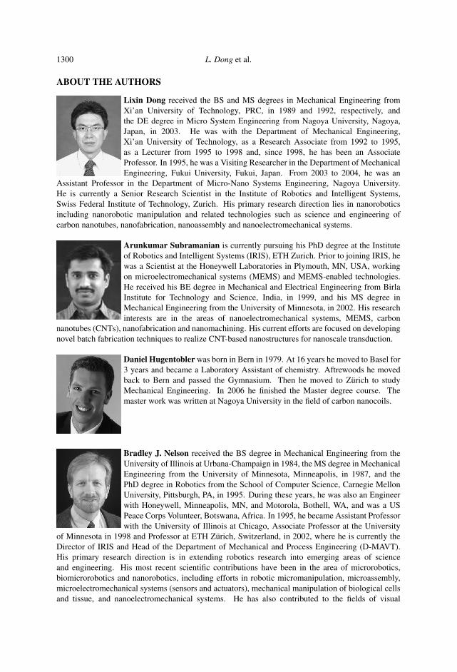
Lixin Dong received the BS and MS degrees in Mechanical Engineering fromXi’an University of Technology, PRC, in 1989 and 1992, respectively, andthe DE degree in Micro System Engineering from Nagoya University, Nagoya,Japan, in 2003. He was with the Department of Mechanical Engineering,Xi’an University of Technology, as a Research Associate from 1992 to 1995,as a Lecturer from 1995 to 1998 and, since 1998, he has been an AssociateProfessor. In 1995, he was a Visiting Researcher in the Department of MechanicalEngineering, Fukui University, Fukui, Japan. From 2003 to 2004, he was an
Assistant Professor in the Department of Micro-Nano Systems Engineering, Nagoya University.He is currently a Senior Research Scientist in the Institute of Robotics and Intelligent Systems,Swiss Federal Institute of Technology, Zurich. His primary research direction lies in nanoroboticsincluding nanorobotic manipulation and related technologies such as science and engineering ofcarbon nanotubes, nanofabrication, nanoassembly and nanoelectromechanical systems.
Arunkumar Subramanian is currently pursuing his PhD degree at the Instituteof Robotics and Intelligent Systems (IRIS), ETH Zurich. Prior to joining IRIS, hewas a Scientist at the Honeywell Laboratories in Plymouth, MN, USA, workingon microelectromechanical systems (MEMS) and MEMS-enabled technologies.He received his BE degree in Mechanical and Electrical Engineering from BirlaInstitute for Technology and Science, India, in 1999, and his MS degree inMechanical Engineering from the University of Minnesota, in 2002. His researchinterests are in the areas of nanoelectromechanical systems, MEMS, carbon
nanotubes (CNTs), nanofabrication and nanomachining. His current efforts are focused on developingnovel batch fabrication techniques to realize CNT-based nanostructures for nanoscale transduction.
Daniel Hugentobler was born in Bern in 1979. At 16 years he moved to Basel for3 years and became a Laboratory Assistant of chemistry. Aftrewoods he movedback to Bern and passed the Gymnasium. Then he moved to Zürich to studyMechanical Engineering. In 2006 he finished the Master degree course. Themaster work was written at Nagoya University in the field of carbon nanocoils.
Bradley J. Nelson received the BS degree in Mechanical Engineering from theUniversity of Illinois at Urbana-Champaign in 1984, the MS degree in MechanicalEngineering from the University of Minnesota, Minneapolis, in 1987, and thePhD degree in Robotics from the School of Computer Science, Carnegie MellonUniversity, Pittsburgh, PA, in 1995. During these years, he was also an Engineerwith Honeywell, Minneapolis, MN, and Motorola, Bothell, WA, and was a USPeace Corps Volunteer, Botswana, Africa. In 1995, he became Assistant Professorwith the University of Illinois at Chicago, Associate Professor at the University
of Minnesota in 1998 and Professor at ETH Zürich, Switzerland, in 2002, where he is currently theDirector of IRIS and Head of the Department of Mechanical and Process Engineering (D-MAVT).His primary research direction is in extending robotics research into emerging areas of scienceand engineering. His most recent scientific contributions have been in the area of microrobotics,biomicrorobotics and nanorobotics, including efforts in robotic micromanipulation, microassembly,microelectromechanical systems (sensors and actuators), mechanical manipulation of biological cellsand tissue, and nanoelectromechanical systems. He has also contributed to the fields of visual
Nano encoders based on arrays of CNTs 1301
servoing, force control, sensor integration, and web-based control and programming of robots. He hasbeen awarded a McKnight Land-Grant Professorship and is a recipient of the Office of Naval ResearchYoung Investigator Award, the National Science Foundation Faculty Early Career Development(CAREER) Award, the McKnight Presidential Fellows Award and the Bronze Tablet. He waselected as a Robotics and Automation Society Distinguished Lecturer in 2003 and received the BestConference Paper Award at the IEEE 2004 International Conference on Robotics and Automation.He was named to the 2005 ‘Scientific American 50’, Scientific American magazine’s annual list thatrecognizes outstanding acts of leadership in science and technology from the past year. He serveson or has been a member of the editorial boards of the IEEE Transaction on Robotics, Journal ofMicromechatronics, The Journal of Optomechatronics and IEEE Robotics and Automation Magazine.He has chaired several international workshops and conferences.
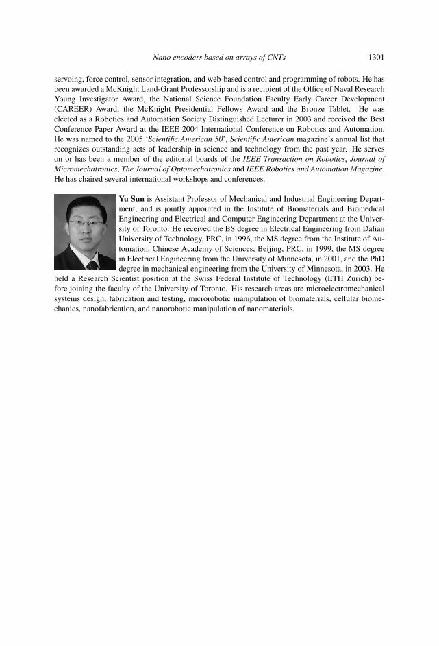
Yu Sun is Assistant Professor of Mechanical and Industrial Engineering Depart-ment, and is jointly appointed in the Institute of Biomaterials and BiomedicalEngineering and Electrical and Computer Engineering Department at the Univer-sity of Toronto. He received the BS degree in Electrical Engineering from DalianUniversity of Technology, PRC, in 1996, the MS degree from the Institute of Au-tomation, Chinese Academy of Sciences, Beijing, PRC, in 1999, the MS degreein Electrical Engineering from the University of Minnesota, in 2001, and the PhDdegree in mechanical engineering from the University of Minnesota, in 2003. He
held a Research Scientist position at the Swiss Federal Institute of Technology (ETH Zurich) be-fore joining the faculty of the University of Toronto. His research areas are microelectromechanicalsystems design, fabrication and testing, microrobotic manipulation of biomaterials, cellular biome-chanics, nanofabrication, and nanorobotic manipulation of nanomaterials.