Embed Size (px)
Citation preview
NANO-SQUID SUSCEPTOMETRY AND FLUCTUATION
EFFECTS IN SUPERCONDUCTING RINGS
A DISSERTATION
SUBMITTED TO THE DEPARTMENT OF APPLIED PHYSICS
AND THE COMMITTEE ON GRADUATE STUDIES
OF STANFORD UNIVERSITY
IN PARTIAL FULFILLMENT OF THE REQUIREMENTS
FOR THE DEGREE OF
DOCTOR OF PHILOSOPHY
Nicholas C. Koshnick
March 2009

c© Copyright by Nicholas C. Koshnick 2009
All Rights Reserved
ii

I certify that I have read this dissertation and that, in my opinion, it
is fully adequate in scope and quality as a dissertation for the degree
of Doctor of Philosophy.
(Kathryn A. Moler) Principal Adviser
I certify that I have read this dissertation and that, in my opinion, it
is fully adequate in scope and quality as a dissertation for the degree
of Doctor of Philosophy.
(Malcolm R. Beasley)
I certify that I have read this dissertation and that, in my opinion, it
is fully adequate in scope and quality as a dissertation for the degree
of Doctor of Philosophy.
(David Goldhaber-Gordon)
Approved for the University Committee on Graduate Studies.
iii
Abstract
This thesis is broken down into two main components: the design and implementa-
tion of two generations of Scanning Superconducting Quantum Interference Device
(SQUID) sensors, and the use of these tools to describe several kinds of fluctuations
that can significantly affect the properties of micron sized aluminum rings.
The first chapter describes the susceptometer that was used for the bulk of the
ring experiments. In it, I outline the advantages of a multi-layer design with local field
coils and integrated feedback loops. To reach the fundamental sensitivity limits set
by Johnson noise in the device itself, I employed piezo electric positioners to measure
background magnetic fields, in addition to taking images of the magnetic field. The
second chapter describes a generation of SQUIDs with FIB-patterned pickup loops
that are connected to a similar base design. The coupling to ultra-small objects is
significantly enhanced by the pickup loop’s small diameter (down to ∼ 600 nm) and
reduced scan height (. 300 nm) enabled by lithographically patterned terraces. When
combined with our device’s low flux noise, this enhanced coupling brings SQUIDs close
to the point where they could distinguish the field from a single electron spin.
Fluctuations are important for superconductors when multiple wave-function con-
figurations need to be considered to describe the overall behavior of the system. This
study includes several experimental regimes where physically distinct energy scales
play an important role. In relatively dirty rings, I show how fluxoid transitions can
significantly reduce the ring’s ability to screen magnetic field. In smaller, cleaner
rings, the contribution from fluxoid modes plays a smaller role, and non-Gaussian
and Gaussian fluctuations induce superconductivity at and above the superconduct-
ing critical temperature, Tc. In this case, I also focus on rings that are biased with half
iv
of a flux quantum of field, which enables two flux modes to contribute to the ring’s
response. I specify the point where thermal fluctuations smear out the Little-Parks
effect, where Tc is reduced due to the Aharonov-Bohm phase winding energy. In the
final section, I report on our efforts to fabricate and measure ultra clean rings where
the Thouless energy is approximately equal to Tc.
v
Acknowledgements
I believe physics is still largely an oral tradition, where we learn from each other
through countless hours of debate. I would like to thank my advisor, Kathryn Moler,
for being the best leader I know in allowing this to happen. She has always been fair
and even in mitigating the inevitable disputes. She has insisted on a lab and group
meeting environment that is energized by debate. This has forced me to re-examine
my assumptions, and has allowed me to connect all I know to basic principles. Finally,
her leadership has influenced us to laugh a bit, and to enjoy both work and play. I
would also like to thank Kam for pushing for certain results, for always requiring us
to rigorously defend our methods, and for teaching me a bit of the art of scientific
writing.
Most of my work was done with the mesoscopics subgroup. I can’t thank Hendrik
Bluhm enough, not only for starting this effort in earnest, but for always being an
active ear and willing debater. Working with him brought me to a higher theoretical
level, and he instilled a certain level of experimental discipline that I would not have
had on my own. I thank Julie Bert, the newest member, for helping with all of the
projects, and in particular for carrying out a lion’s share of work in screening the
nano-SQUIDs presented in chapter 3. Her discipline and competence will lead to
exciting results in the years to come.
There are many people outside of our lab who have played a large role in allowing
my work to happen. Most notably is Martin Huber, who worked with me on the
nano-SQUID design and completed all of the optical fabrication steps. Much of my
mastery of SQUID technologies, such as SQUID array amplifiers, is directly related to
his influence. I also thank Hal Edwards, Jeff Large, and Steve O’Connel for working
vi
with us to establish a FIB fabrication method when it was clear an E-beam approach
would not work.
Many people have helped me understand fluctuations in superconducting rings.
Foremost, I thank Xiaxian Zhang and John Price. Their work in the mid 90’s laid the
foundation for almost all of our work. Conversations with John led us to anticipate
the effects of SQUID radiation, and to consider bilayered samples as an attractive
candidate material for making rings (see chapter 6). I thank Georg Schwiete for
patiently teaching me almost everything I know about non-gaussian fluctuations, and
Jorge Berger for organizing a conference on the subject, and following up on the work
with correspondence and work of inhomogeneities.
Moler lab members, both past and present, have been like an extended family.
Ophir Auslaender, Brian Gardner, Lan Luan, and Clifford Hicks in particular have
taught me numerous things, daily. I thank all my Physics/Applied Physics friends for
shaping my understanding and, of course, all the faculty for their teaching efforts. All
the McCullough basement dwellers, and in particular Ron Potok and Myles Steiner
for teaching me general lab techniques and basic lithography, respectively. James
Conway has gone beyond the call of duty to help keep the ebeam writer working
well, and Bob Hammond and Tom Carver have been invaluable for their knowledge
of metallurgy. The GLAM/CPN staff Laraine Lietz-Lucas, Cyndi Mata Barnett, and
Stephen Swisher for cutting the red tape, and Kyle Cole for giving me numerous
outreach opportunities, and reminding me of how much I love to teach.
I want to thank my reading committee members, Mac Beasley and David Goldhaber-
Gordon, for being there to lend a supportive ear with many pointers along the way.
Mac’s superconductivity class and David’s mesoscopics reading class were two of the
best and most useful classes I took at Stanford.
Finally, I would like to thank my Mom, who is one of the most creative people
I know, and who worked to instill that quality in me from a young age. My Dad,
who taught me to be a diligent student, to calculate things in the back of my head,
and to always come to my own conclusions. And Maureen, who has broadened and
redoubled my interest in both science and new technologies, and who has taught me
a bit about how to be a passionate human as well as a good scientist.
vii
Contents
Abstract iv
Acknowledgements vi
1 Overview and introduction 1
2 Symmetric SQUID susceptometer 5
2.1 Introduction . . . . . . . . . . . . . . . . . . . . . . . . . . . . . . . . 6
2.2 Design . . . . . . . . . . . . . . . . . . . . . . . . . . . . . . . . . . . 9
2.3 Experimental System . . . . . . . . . . . . . . . . . . . . . . . . . . . 13
2.4 Noise Design and Performance . . . . . . . . . . . . . . . . . . . . . . 14
2.4.1 Measured Flux sensitivity . . . . . . . . . . . . . . . . . . . . 15
2.4.2 Bandwidth . . . . . . . . . . . . . . . . . . . . . . . . . . . . 17
2.5 Imaging and Coupling to Mesoscopic Samples . . . . . . . . . . . . . 17
2.6 Conclusion . . . . . . . . . . . . . . . . . . . . . . . . . . . . . . . . . 21
3 Sub-Micron Terraced Susceptometer 22
3.1 Sub-Micron Terraced Susceptometer . . . . . . . . . . . . . . . . . . . 22
3.2 NanoSQUID supplemental Material . . . . . . . . . . . . . . . . . . . 28
3.2.1 FIB fabrication . . . . . . . . . . . . . . . . . . . . . . . . . . 29
3.2.2 Layer Thickness Effects . . . . . . . . . . . . . . . . . . . . . . 29
3.2.3 Cooling fins . . . . . . . . . . . . . . . . . . . . . . . . . . . . 32
viii
4 Fluctuation Superconductivity in Rings 35
4.1 Fluctuation Induced Superconductivity in Rings . . . . . . . . . . . . 35
4.2 Fluctuation Induced Superconductivity Supplement . . . . . . . . . . 45
4.2.1 Materials and Methods . . . . . . . . . . . . . . . . . . . . . . 46
4.2.2 Supplemental Online Text . . . . . . . . . . . . . . . . . . . . 49
5 Fluxoid Fluctuations 54
5.1 Introduction . . . . . . . . . . . . . . . . . . . . . . . . . . . . . . . . 55
5.2 Experimental Results . . . . . . . . . . . . . . . . . . . . . . . . . . . 56
5.3 The Fluxoid Fluctuation Transition . . . . . . . . . . . . . . . . . . . 58
5.4 Relating Fluxoid and Non-Fluxoid Fluctuations . . . . . . . . . . . . 59
5.5 Conditions for Equilibrium . . . . . . . . . . . . . . . . . . . . . . . . 65
6 Towards Superconducting Rings Where Ec > kBTc 67
6.1 Theoretical Background . . . . . . . . . . . . . . . . . . . . . . . . . 68
6.1.1 Clean Wide Rings: T < Ec ≈ kBTc . . . . . . . . . . . . . . . 68
6.1.2 Bilayers: T < Tc < Ec . . . . . . . . . . . . . . . . . . . . . . 70
6.2 Sputtered Aluminum Rings . . . . . . . . . . . . . . . . . . . . . . . 72
6.3 Normal Metal/Superconductor Bilayer Rings . . . . . . . . . . . . . . 75
A 1/f-like Noise in Our System 78
A.1 Low frequency noise observations . . . . . . . . . . . . . . . . . . . . 79
A.2 Calculation of low-f noise from nearby metal . . . . . . . . . . . . . . 80
B Concepts for future scanning SQUID designs 83
B.1 Advantages of a planarized sub-micron design . . . . . . . . . . . . . 85
B.2 Reducing the SQUID’s self-inductance . . . . . . . . . . . . . . . . . 88
B.3 Reducing SQUID sample back action . . . . . . . . . . . . . . . . . . 90
Bibliography 93
ix

List of Tables
3.1 Survey of reported scanning SQUIDs and their spin sensitivities . . . 24
3.2 Layer thicknesses of the two processed wafers. . . . . . . . . . . . . . 32
4.1 Table of measured and fitted ring parameters . . . . . . . . . . . . . . 47
4.2 Mutual inductances calculated with a Fast Henry . . . . . . . . . . . 48
6.1 Table of Al properties after 3 fabrication conditions . . . . . . . . . . 73
x

List of Figures
2.1 Digrams of dipole and ring field lines, pickup loop, and susceptometer. 8
2.2 Micrograph of 4.6 micron SQUID . . . . . . . . . . . . . . . . . . . . 11
2.3 Circuit diagram for the device operation . . . . . . . . . . . . . . . . 13
2.4 SQUID Current-Voltage Characteristics . . . . . . . . . . . . . . . . . 14
2.5 Noise spectrum and white noise versus temperature . . . . . . . . . . 16
2.6 Images of vortices, rings, and meander wires . . . . . . . . . . . . . . 18
2.7 Linear susceptibility of a gold ring . . . . . . . . . . . . . . . . . . . . 20
3.1 Images of FIB and 3.2 micron optical SQUID. . . . . . . . . . . . . . 26
3.2 FIB SQUID magnetometry images. . . . . . . . . . . . . . . . . . . . 27
3.3 FIB fabrication details . . . . . . . . . . . . . . . . . . . . . . . . . . 30
3.4 Diagram of layer thickness effects . . . . . . . . . . . . . . . . . . . . 31
3.5 Cooling fins and white noise temperature dependence. . . . . . . . . . 33
4.1 Diagram and artists rendition a scanning SQUID over rings. . . . . . 38
4.2 SQUID response versus applied flux. . . . . . . . . . . . . . . . . . . 39
4.3 Susceptibility as a function of temperature. . . . . . . . . . . . . . . . 42
4.4 Φ− I data showing Little-Parks effect washed out for large γ rings. . 44
5.1 Data of fluxoid fluctuation reduced response. . . . . . . . . . . . . . . 57
5.2 The susceptibility at Tc as predicted by the von Oppen theory . . . . 60
5.3 Theoretical response from London, fluxoid, von Oppen, and HO models. 62
5.4 Fluxoid and saddle points energies versus applied flux. . . . . . . . . 66
6.1 Tc as a function of applied flux. . . . . . . . . . . . . . . . . . . . . . 69
xi

6.2 Sputtered Al fabrication and properties . . . . . . . . . . . . . . . . . 74
6.3 Co/Mo bilayer fabrication. . . . . . . . . . . . . . . . . . . . . . . . . 76
A.1 Low frequency noise in our SQUIDs and SQUID arrays, and electronics. 79
B.1 Planarized layer effects and an improved sub-micron design . . . . . . 86
B.2 Simplified flux coupled SQUID model . . . . . . . . . . . . . . . . . . 89
xii
Chapter 1
Overview and introduction
This thesis describes superconducting fluctuation effects in micron-sized aluminum
rings. The rings were studied experimentally using a SQUID, or Superconducting
Quantum Interference Device, which at the simplest level is simply a tool that mea-
sures magnetic field. We fabricate these SQUIDs on one wafer, and polish it so that
the active area of the device is near the corner. We fabricate the rings on a separate
wafer, and bring the SQUID down over each ring, measuring the ring’s response to
an applied field, one at a time. The device used for these measurements, and some
details of the technique, will be the subject of chapter 2. Chapter 3 describes a new
SQUID that is smaller and closer to the sample, allowing for a much better spin sensi-
tivity. These two published papers include historical references, and appendix B puts
these devices in the context of our ideas for future work. This introduction will begin
with a broader introduction to superconductivity, from which the basic properties
of SQUIDs can be derived. Since numerous books [21] review both the basics and
intricacies or SQUID design, this chapter is focused on the historical importance of
fluctuation effects in superconductors, and their broad relation to the work presented
in chapters 4, 5, and 6.
Low temperature experiments have allowed physicists to measure many exotic
states of matter. One of the most dramatic effects is the phenomenon of supercon-
ductivity. Superconductivity occurs when a suitable material is cooled below some
critical temperature, Tc, which allows the electrons to undergo a phase transition
1
CHAPTER 1. OVERVIEW AND INTRODUCTION 2
to a state where they behave cooperatively. Once superconductivity occurs, their
collective behavior can be described by a macroscopic quantum wave function.
Superconductivity has three hallmark properties. Below the transition temper-
ature, superconductors have zero resistance and they screen magnetic field (the so
called Meissner effect). The final hallmark is flux quantization. If a very large
magnetic field is applied to a superconductor, the part that goes through the ma-
terial is forced to go through in quantized bundles, called vortices. This trait relates
to the fact that superconductors can be described by a single valued wave func-
tion, Ψ, that is a function of space and is characterized by magnitude and a phase
Ψ(x) = |Ψ(x)| exp(iφ(x)). The phase at any location has a single value between zero
and 2π. This implies that if you follow the phase around any normal metal region,
the value of that phase must wind an integer number of times. Vortices correspond
to one winding, each associated with one flux quantum of magnetic field. As we will
see, rings can have more than one winding especially when a magnetic field is applied.
The Josephson equations describe how a change in the phase, φ, can create a
voltage. Vortex motion across a superconductor is thus associated with voltage, or
resistance. Similarly, it is the phase winding in the Josephson junctions of our SQUIDs
that give us the voltage through which we measure magnetic field.
Fluctuations are important because they can make the hallmarks of supercon-
ductivity occur at a different temperature than the temperature predicted by the
microscopic mechanisms for superconductivity in a given material. The Berezinsky-
Kosterlitz-Thouless (BKT) transition is a good example of this: In sufficiently thin
two dimensional superconductors, the BKT effect explains how thermal energy can
create vortex-anti-vortex pairs, and how those pairs can become physically separated
from each other in the superconductor. As the vortex pairs start proliferating and
annihilating, the vortex motion causes resistance. The pair motion also means that
relative phase is not well defined across the superconductor, and the superconductor
is no longer very effective at screening magnetic field.
Fluctuation superconductivity was being worked out in the late 1970’s, and early
1980’s [54], but the focus of superconductivity research shifted dramatically when so
called high temperature superconductivity (High-Tc) was discovered [7] on the eve of
CHAPTER 1. OVERVIEW AND INTRODUCTION 3
1987. Interest in the field has increased again in the last ten years, because of the
role superconducting fluctuations may play in the High-Tc phase diagram [26]. This
is particularily true in the pseudo-gap regime where some form of superconductivity
may exist but there is no global phase coherence or zero resistance.
This thesis focuses on one dimensional (1D) superconductors. In this case 1D
implies the crossection of a superconductor is less than the penetration depth, λ, and
the coherence length, ξ, each typically more than 100 nm in aluminum. In 1D, one
only needs to consider variations along the linear dimension. Our rings are simply a
one dimensional wire that is wrapped around on itself. The ring’s 1D nature provides
a simplified model system, with solutions that are theoretically tractable. Measuring
a ring’s response to magnetic field also access to certain thermodynamic properties
that can not be accessed directly with standard resistance measurements.
Generally, we say fluctuations are important when one needs to consider multiple
wave function solutions to describe the behavior of the system. In 1D wires, fluc-
tuations are very important because solutions along the wire with different phase
windings have nearly identical energies. Thermal energy can also induce a momen-
tary weak point in the superconductor allowing the phase to change [53]. Since phase
change gives voltage, 1D wires can have finite resistance well below the nominal crit-
ical temperature, and above Tc there are electron pair correlations along the wire,
which makes the transition very broad. These effects have been studied to great
length with transport measurements, with a large part of the recent work focussed
on the nature of the phase slip initiation [10]. Relatively less work has been done at
and above Tc.
In this thesis, I have studied the intimate relation between phase and amplitude
in uniform rings. In chapter 5, I describe relatively long, dirty rings, where thermal
energy can cause the population of multiple phase winding solutions reducing the
ring’s ability to screen magnetic field. In chapter 4, I discribe a range of moderately
clean rings, where phase winding is so costly that superconductivity is destroyed
(the Little-Parks effect), leaving a remnant fluctuation induced response above the
reduced flux-dependent Tc. In chapter 6, I present work towards the realization of
even cleaner rings, with both large and small amplitudes, where it may one day be
CHAPTER 1. OVERVIEW AND INTRODUCTION 4
possible to observe quantum induced fluctuations.
The SQUID described in chapter 2 was designed and implemented by Martin Hu-
ber. My major contributions were in the development of the scanning technique, the
interpretation of the fundamental noise sources, and to the formulation and writing
of the paper. The SQUID described in chapter 3 was designed primarily by myself,
with some design help and all of the optical fabrication done by Martin Huber. The
FIB fabrication was done first in Jeff Large’s group at Texas Instruments, and then
later by myself at Stanford. Julie Bert did the initial screening of most of the de-
vices, and aquired the noise data presented in figure 3.2g. The data in chapters 4,
5, and 6 was taken with a scanning microscope in the dilution refrigerator originally
designed and implemented by Per Bjornsson [11]. Hendrik Bluhm added the course
motion and wrote much of the scanning and data acquisition software. Hendrik and I
participated roughly equally in debugging the system, enhancing the ability to apply
large currents, and reducing the system’s noise. The samples for both of these exper-
iments were made by myself, and I did almost all of the data interpretation, with the
notable exception of the initial fluxoid fluctuation idea, which came from Hendrik.
The bilayer idea, chapter 6, was originally suggested by John Price at the University
of Colorado - Boulder. Sorting out the low-frequency noise components, appendix
A, was done collaboratively with Jason Pelc, and the section on concepts for future
SQUIDs, appendix B, benefited greatly from discussions with, and the ongoing design
by John Kirtley.
Chapter 2
Gradiometric micro-SQUID
susceptometer for scanning
measurements of mesoscopic
samples
Martin E. Huber, Nicholas C. Koshnick, Hendrik Bluhm, Leonard J. Archuleta,
Tommy Azua, Per G. Bjornsson, Brian W. Gardner, Sean T. Halloran, Erik A. Lucero
and Kathryn A. Moler
Review of Scientific Instruments, 79, 053704 (2008)
We have fabricated and characterized micro-SQUID susceptometers for use in low-
temperature scanning probe microscopy systems. The design features the following:
a 4 µm sensor loop; a field loop to apply a local field to the sample; an additional
counter-wound sensor-loop/field-loop pair to cancel the background signal from the
applied field in the absence of the sample; modulation loops to allow setting the
SQUID at its optimum bias point (independent of the applied field), and shielding
that minimizes coupling of magnetic fields into the leads and body of the SQUID. The
design is highly symmetric to cancel the flux signal from uniform external fields. We
use a SQUID series array preamplifier and obtain a system bandwidth of 1 MHz. The
5
CHAPTER 2. SYMMETRIC SQUID SUSCEPTOMETER 6
flux noise at 125 mK is approximately 0.25 µΦ0/√Hz above 10 kHz, with a value of
2.5 µΦ0/√Hz at 10 Hz.
2.1 Introduction
The magnetic response of micro- and nano-scale objects, as a function of an applied
magnetic field, reveals properties that cannot be probed directly by other methods.
For instance, the current in a mesoscopic ring is the first derivative of the rings
free energy with respect to magnetic flux, allowing for the study of fundamental
thermodynamic properties [49]. The periodicity of the free energy with respect to the
flux quantum allows for a variety of fluxoid physics, including the Little-Parks effect
[56], multiple fluxoid transitions [17], and the detection of novel superconducting wave
function states.[16] The intrinsic sensitivity of Superconducting Quantum Interference
Devices (SQUIDs) to magnetic flux makes these devices some of the world’s best
instruments for measuring magnetic fields [21]. In this paper we present a scanning
SQUID susceptometer that has enabled results [49, 17, 16] on micron scale objects in
part because it is specifically designed to measure the response of small objects as a
function of applied field.
Micro-SQUIDs excel at quantitative measurement of small magnetic signals, and
scanning SQUID microscopy is often used for imaging.[47] Our devices have been
used for such studies in the past [12], we emphasize design aspects that a scanning
system can also be used to measure the total magnetic response to applied field
(moment or susceptibility) of nanoscale objects, which has more traditionally been
done with non-scanning sensors that may be integrated onto the same chip as the
sample [59], require physical placement of a sample in the sensor loop [6], or in a
static flip-chip geometry.[90] Use of a scanning sensor has multiple advantages for
this purpose, allowing measurement of samples that are on different substrates or
that can be fabricated by incompatible processes, as well as measurement of multiple
samples in a single cool-down. Most importantly for the smallest signals, a scanning
sensor allows in situ measurements of the background simply by moving away from
the sample.
CHAPTER 2. SYMMETRIC SQUID SUSCEPTOMETER 7
All SQUIDs have nonlinear current-voltage characteristics with a critical current
that depends periodically on the total flux Φ through the SQUID loop with a period-
icity of the superconducting flux quantum, Φ0 = h/2e. The smallest micro-SQUIDs
fabricated to date are also the most basic, consisting of a simple superconducting loop
with two Josephson junctions or microbridges [22, 52, 87]. The single-loop designs are
hysteretic because they lack shunt resistors (in the case of tunnel junctions) or have
intrinsic heating issues (associated with hot quasiparticles in microbridges). Because
it is not possible to use a feedback circuit to keep the SQUID in a flux locked loop
when there are no modulation loops, the response of simple SQUIDs is non-linear in
applied field. In principle, shunt resistors and a modulation loop could be added, but
in practice, it is difficult to fabricate shunt resistors into a small region and modu-
lation loops have limited use because the modulation field is applied to the sample
as well. Fabricating a sensor loop that is separate from the core area of the SQUID
solves both of these problems.
SQUIDs with independent control of sample flux and bias flux allow for operation
at the maximum-sensitivity bias point for all measurement fields. We have designed
our device with separate sensor/field loops (for applying fields to the sample and
measuring the sample’s response) and modulation loops (for setting the flux bias of
the SQUID). These two sets of loops are separated in space to reduce cross-coupling
and are arranged as gradiometers to reduce coupling to external magnetic fields.
Coupling the sensor loop directly to the main body of the SQUID through integrated
coaxial leads [43] results in the scanning SQUID magnetometer design reported by
Kirtley and Ketchen. Separating the sensor loop and the junction body also allows
the sensor loop to be optimized for coupling to the sample.
In many cases, it is desirable to null the SQUID’s response to the applied field
so that the signal only reflects the magnetic response of the sample to the applied
field. This can be done by including a separate, counter-wound sensor-loop/field-
loop pair to cancel the applied field. Designs including such features are known as
SQUID susceptometers and were first proposed and produced by Ketchen [43] and
implemented in a scanning geometry by Gardner et al [28]. The previously reported
design had 8 µm sensor loops and did not have a high degree of symmetry.
CHAPTER 2. SYMMETRIC SQUID SUSCEPTOMETER 8
We report on the design, fabrication, and characterization of scanning SQUID
susceptometers with 4 µm sensor loops, integral and robust shielding, and a high
degree of symmetry. Section 2.2 will describe design considerations. Section 2.3
will describe the experimental configuration, including the scanning stage and pre-
amplifier with which we could achieve the same intrinsic flux noise while scanning as
while in a static, well-shielded environment. Section 2.4 will describe the flux noise
optimization process and background cancellation technique. Section 2.5 will describe
images taken by this device which will allow for the description of the pick-up loop
imaging kernel and will describe the spin and ring-current sensitivities.
Field
Coils
Mod.
Coils
Pickup
Loop
a
b
c
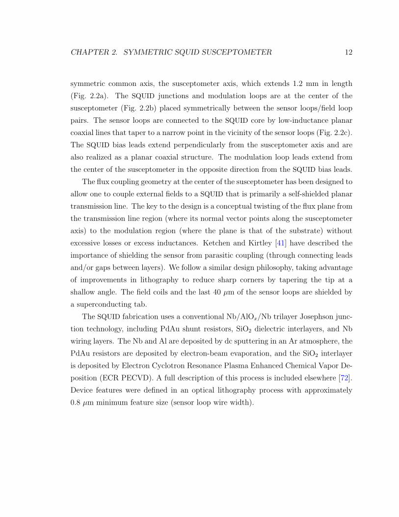
Figure 2.1: (a) Field lines (red) from a current I in a ring positioned on axis butslightly below the sensor loop (black), with shielding tab shown in gray. (b) Fieldlines (red) from dipole moment of a sample located at the center of a sensor loop(black). The inclosed flux increases as the loop diameter is decreased. The netflux also increase if the sample is moved toward the wire forming the sensor loop.(c) Simplified diagram of the device, showing the general relationship between thesensor loops, the field loops, and the modulation loops. The center-tap of the fieldcoils allows compensation of lithographic imperfections between the two sensor loops.The blue/gray shading represents the low inductance planar coaxial shield on thesusceptometer arms.
CHAPTER 2. SYMMETRIC SQUID SUSCEPTOMETER 9
2.2 Design
SQUIDs are intrinsically sensitive to the magnetic flux threading their pickup area,
thus the best field sensitivity is achieved with the largest pickup area compatible
with a given application. While large SQUIDs have the best sensitivity to magnetic
field, small SQUIDs have better coupling to small samples. Our 4 µm sensor loop
size allows for a large pickup loop area relative to the lithographically-limited spacing
between the pickup loop leads, allowing for an convenient scan-imaging kernel. It
also allows for optimal coupling to micron-scale samples, such as rings, where fields
. 50 Oe (where vortices move in the SQUID) can apply several supercontucting
flux quantum, Φ0, through a given sample’s center. When the sample’s diameter
is sufficiently small compared to the pickup loop size (Fig. 2.1a) the field lines can
be approximated as an ideal dipole (Fig. 2.1b). When the dipole moment, m, is in
the center of the pickup loop and aligned perpendicular to the pickup loop plane as
shown, the magnetic flux captured by the sensor is ΦSQ = mrd/R where R is the
radius of the ring, rcl = 2.8× 10⁻¹⁵ m is the classical electron radius, ΦSQ is in units
of Φ0 and m is in units of electron spins, µB [41]. Qualitatively, smaller sensor loops
allow fewer field lines to close within the sensor area, increasing the total magnetic
flux threading the loop. The coupling decreases rapidly if the dipole is more than the
pickup loop radius away from the plane of the sensor loop. Maximal coupling occurs
when the dipole is directly next to the sensor loop itself, at which point, the Meissner
screening associated with the sensor loop line-width can play an important role and
more accurate modeling[40] is required to estimate an accurate spin sensitivity.
To measure the magnetic response of a sample as a function of applied field, the
measurement process must cancel the sensor’s response to the applied field itself.
To aid this cancellation process, our susceptometer is designed with two, nominally
identical, counter-wound sensor loops, separated by ≈ 1.2 mm on the sensor chip so
that one loop can be located in close proximity to the sample while the other loop is
far from the sample substrate to avoid unwanted coupling [Fig. 2.1c]. The symmetry
of the design leads to both a geometric cancellation of a uniform applied field and a
balanced inductance between the two arms of the SQUID, which leads to improved
CHAPTER 2. SYMMETRIC SQUID SUSCEPTOMETER 10
electrical performance.
We apply field to the area near the two sensor loops with local single-turn field
loops that are fully integrated into the SQUID chip layout. The inner diameter of
each field loop is 10 µm, or approximately twice the diameter of the sensor loop,
allowing for a mutual inductance of 2 pH or ≈ 1 Φ0/mA. The field at the center of
the loop is approximately 1 Gauss/mA. Although the critical current of the field coil
lines is IFC ≈ 75 mA, effective operation is limited to a range IFC . ±45 mA due to
the onset of vortex motion. The field loops are fabricated from a thin-film Nb layer
deposited directly on the substrate so as to avoid edge crossings that might decrease
the critical current of the lines. The vortex motion is thus likely to occur in one of
the shielding layers as described the next section.
The two field loops are connected in series, so that a constant current applies the
same magnetic induction to both sensor loops. A geometric imbalance of approxi-
mately 1 part in 100 is thought to be caused by lithographic imperfections. A center
tap on the field loop leads allows one to cancel the residual geometric coupling between
field loops and sensor loops to within 1 part in 10,000. At this level of cancellation,
we are able to apply ∼ 40 Φ0 of field with a residual signal of only a few mΦ0. This
allows for sufficient dynamic range in the preamplifier/readout electronics to measure
the residual background with the same sensitivity as we measure the signal itself.
The local field coils have three additional advantages when compared to a system
which operates in a uniform field applied by an external solenoid. First, the inte-
grated field coils have a comparatively low inductance which enables the possibility
of oscillating the applied field at a high rate (∼ 10 kHz), alleviating many of the
problems associated with low frequency sensor noise. Second, because the field from
the field coils falls off like 1/r3 when the distance from the sample, r, is larger than
the field coil diameter, the coupling to the sample is proportional to 1/r6 (as opposed
to 1/r3 for a uniform field). This allows for a more independent characterization of
the SQUIDs response to the applied field in situ away from any sample. Finally, the
local field coils allow for the modulation loops and Josephson junctions to operate in
a low field environment.
CHAPTER 2. SYMMETRIC SQUID SUSCEPTOMETER 11
Integrated modulation loops allow for operation in a flux locked loop. The feed-
back technique linearizes the response in the applied flux and allows the SQUID to
operate at a flux bias point of optimal sensitivity [21]. The modulation loops are
larger than the applied field loops, reducing the feedback current requirements, and
thus the heating from stray resistances in the low temperature wiring. Although the
modulation loops cancel off constant background fields with their gradiometric de-
sign, they are still highly sensitive to gradients in the applied field due to their large
size, thus we find that scanning mount vibrations of approximately 25 nm magnitude
limit the sensitivity of the system when it is operated in a field applied by an external
solenoid.
a b
c
Mod.
Loops
Shunt
Resistor
Tunnel
Junction
5 µm
200 µm
20 µm
Figure 2.2: (a) Photomicrogaph of the full device, prior to polishing the tip. Pads forwirebonding are at the top. The distance between sensor loops is 1.2 mm. The fieldcoil lines approach each sensor coil from a 45 degree angle to the axis; the modulationcoils approach coupling loops in the center of the SQUID perpendicular to the axis.(b) Close-up view of the core area of the SQUID, including junctions, shunt resistors,and modulation loops. (c) Close-up view of the sensor area, after polishing. Noteshielding layers above both the sensor loop leads and the field loop leads.
The gradiometric sensor loops and like-polarity field loops form the ends of a
CHAPTER 2. SYMMETRIC SQUID SUSCEPTOMETER 12
symmetric common axis, the susceptometer axis, which extends 1.2 mm in length
(Fig. 2.2a). The SQUID junctions and modulation loops are at the center of the
susceptometer (Fig. 2.2b) placed symmetrically between the sensor loops/field loop
pairs. The sensor loops are connected to the SQUID core by low-inductance planar
coaxial lines that taper to a narrow point in the vicinity of the sensor loops (Fig. 2.2c).
The SQUID bias leads extend perpendicularly from the susceptometer axis and are
also realized as a planar coaxial structure. The modulation loop leads extend from
the center of the susceptometer in the opposite direction from the SQUID bias leads.
The flux coupling geometry at the center of the susceptometer has been designed to
allow one to couple external fields to a SQUID that is primarily a self-shielded planar
transmission line. The key to the design is a conceptual twisting of the flux plane from
the transmission line region (where its normal vector points along the susceptometer
axis) to the modulation region (where the plane is that of the substrate) without
excessive losses or excess inductances. Ketchen and Kirtley [41] have described the
importance of shielding the sensor from parasitic coupling (through connecting leads
and/or gaps between layers). We follow a similar design philosophy, taking advantage
of improvements in lithography to reduce sharp corners by tapering the tip at a
shallow angle. The field coils and the last 40 µm of the sensor loops are shielded by
a superconducting tab.
The SQUID fabrication uses a conventional Nb/AlOx/Nb trilayer Josephson junc-
tion technology, including PdAu shunt resistors, SiO2 dielectric interlayers, and Nb
wiring layers. The Nb and Al are deposited by dc sputtering in an Ar atmosphere, the
PdAu resistors are deposited by electron-beam evaporation, and the SiO2 interlayer
is deposited by Electron Cyclotron Resonance Plasma Enhanced Chemical Vapor De-
position (ECR PECVD). A full description of this process is included elsewhere [72].
Device features were defined in an optical lithography process with approximately
0.8 µm minimum feature size (sensor loop wire width).
CHAPTER 2. SYMMETRIC SQUID SUSCEPTOMETER 13
2.3 Experimental System
The field loop leads are oriented at a 45 angle to the axis of the SQUID so that the
susceptometer may be polished to approximately 15 µm of the field coil so that the
sensor loop is near the edge of the chip. The device is then fastened to a cantilever
and aligned at an angle of approximately 2 with respect to the sample plane so that
the sensor loop can be positioned in close proximity ( ∼1 µm) to the sample. The
cantilever movement is controlled by a large area scanning piezoelectric S-bender [77]
with additional coarse motion control by stick-slip motion attocube positioners [1].
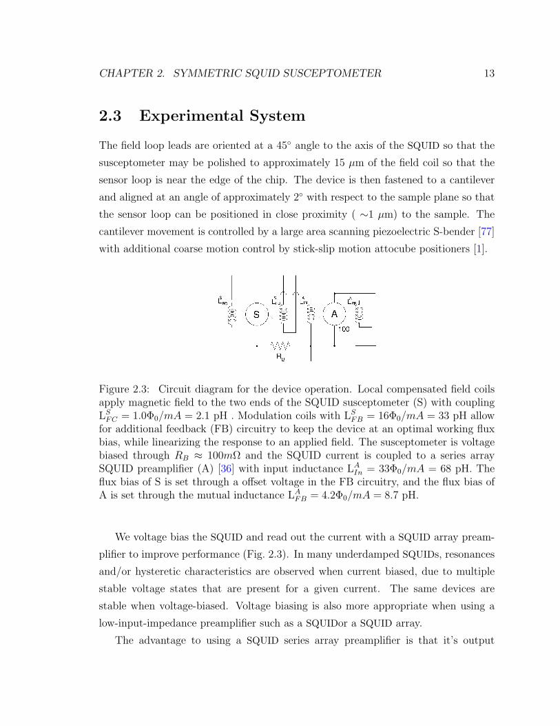
Figure 2.3: Circuit diagram for the device operation. Local compensated field coilsapply magnetic field to the two ends of the SQUID susceptometer (S) with couplingLSFC = 1.0Φ0/mA = 2.1 pH . Modulation coils with LSFB = 16Φ0/mA = 33 pH allowfor additional feedback (FB) circuitry to keep the device at an optimal working fluxbias, while linearizing the response to an applied field. The susceptometer is voltagebiased through RB ≈ 100mΩ and the SQUID current is coupled to a series arraySQUID preamplifier (A) [36] with input inductance LAIn = 33Φ0/mA = 68 pH. Theflux bias of S is set through a offset voltage in the FB circuitry, and the flux bias ofA is set through the mutual inductance LAFB = 4.2Φ0/mA = 8.7 pH.
We voltage bias the SQUID and read out the current with a SQUID array pream-
plifier to improve performance (Fig. 2.3). In many underdamped SQUIDs, resonances
and/or hysteretic characteristics are observed when current biased, due to multiple
stable voltage states that are present for a given current. The same devices are
stable when voltage-biased. Voltage biasing is also more appropriate when using a
low-input-impedance preamplifier such as a SQUIDor a SQUID array.
The advantage to using a SQUID series array preamplifier is that it’s output
CHAPTER 2. SYMMETRIC SQUID SUSCEPTOMETER 14
impedance is designed to couple well to room-temperature electronics. Thus, there
is no need for an impedance-matching transformer that might limit the bandwidth.
Moreover, the feedback circuit can be directly coupled, without use of a modulation
frequency. We use a N = 100 SQUID series array [36] with an output impedance
of ∼ 300Ω. When the array is operated in a magnetically shielded environment, a
minimal amount of flux trapping occurs and the combined output from all of the
SQUIDs is in phase, and thus adds coherently to the total signal. The input current
sensitivity of the SQUID series array is approximately 2.5 pA/√Hz with a 1/f knee at
∼ 50 Hz. This measured noise is less than the fundamental noise of the susceptometer.
2.4 Noise Design and Performance
0 10 20 300
5
10
15
20
25
30
35
Φ = 0
Φ0/4
Φ0/2I S
Q (
µA)
VSQ
(µV)
−35 0 3510
15
20
Imod
(µA)
I SQ
(µA
)
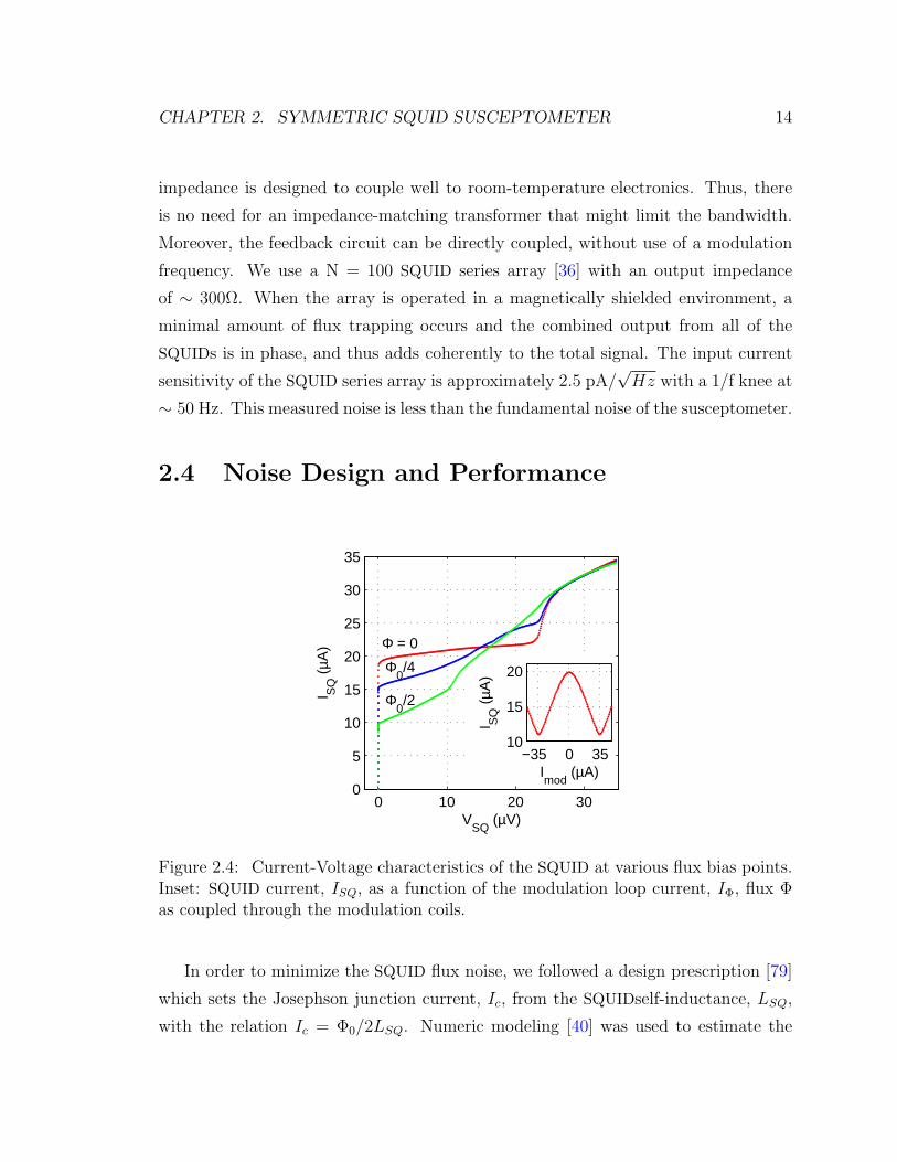
Figure 2.4: Current-Voltage characteristics of the SQUID at various flux bias points.Inset: SQUID current, ISQ, as a function of the modulation loop current, IΦ, flux Φas coupled through the modulation coils.
In order to minimize the SQUID flux noise, we followed a design prescription [79]
which sets the Josephson junction current, Ic, from the SQUIDself-inductance, LSQ,
with the relation Ic = Φ0/2LSQ. Numeric modeling [40] was used to estimate the
CHAPTER 2. SYMMETRIC SQUID SUSCEPTOMETER 15
inductance of individual SQUID components yielding: modulation core region, 55
pH, strip line, 9 pH/mm, tapper region, 4 pH , pickup loop, 13 pH. The combined
inductance LSQ ≈ 100pH agrees to within experimental uncertainty of the actual
inducatance, as extrapolated [67] from the critical currents at applied flux values of
Φ = 0 and Φ0/2. The corresponding design Ic ≈ 10 µA agrees well with the measured
Max(Ic/2) as shown in figure 2.4a. Using the same design prescription, Shunted DC
SQUIDs are non-Hysteretic when the parameter βC = 2πIcR2CJ/Φ0 ≤ 1, where CJ
is the capacitance of each junction. We report on our lowest resistance (RSQ = 1.2Ω)
devices which have a non-hysteretic response and the measured noise performance.
The choices give a design value of βL = 1 and βC = 0.3. The dynamic resistance
under a common operating bias is approximately 3.5 Ω.
A bias resistor of approximately 100 mΩ is fabricated on the same substrate as
the susceptometer. This resistor is not used at ultra-low temperatures where heat
loading is an issue.
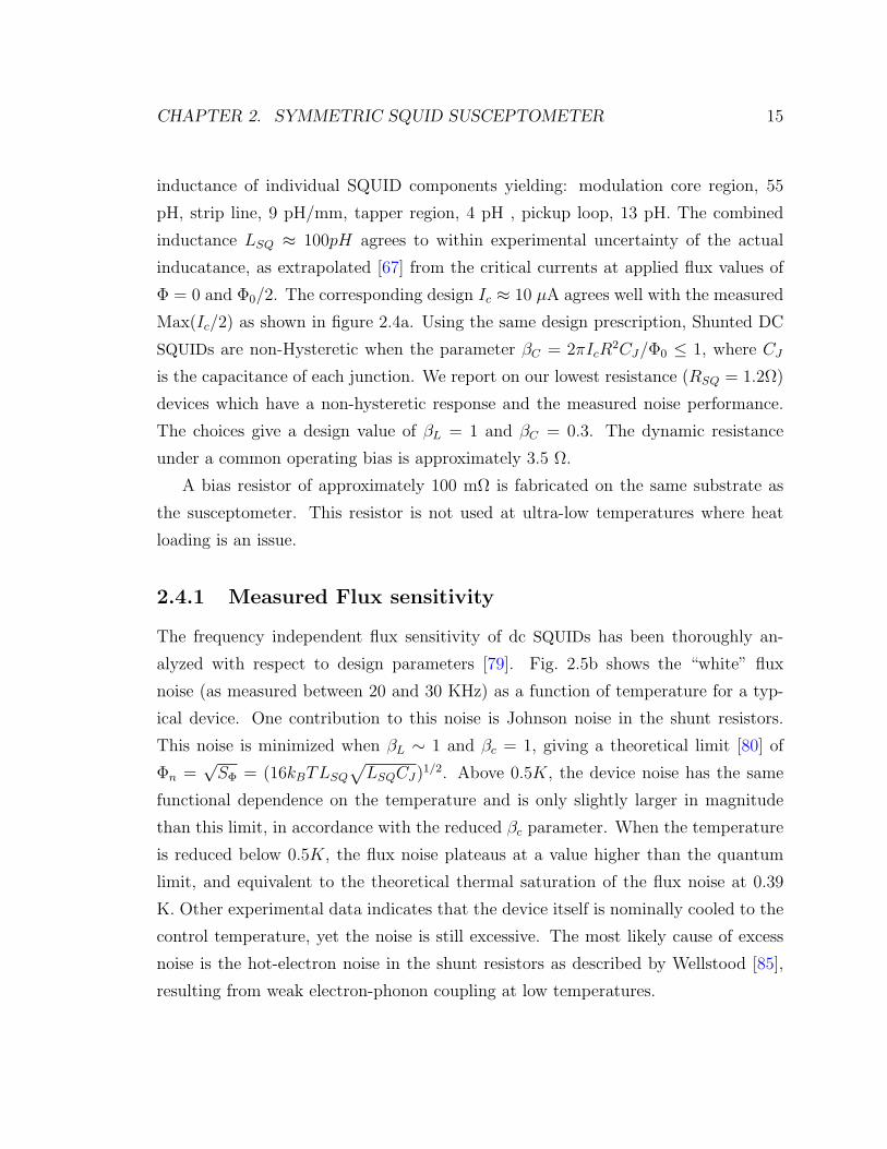
2.4.1 Measured Flux sensitivity
The frequency independent flux sensitivity of dc SQUIDs has been thoroughly an-
alyzed with respect to design parameters [79]. Fig. 2.5b shows the “white” flux
noise (as measured between 20 and 30 KHz) as a function of temperature for a typ-
ical device. One contribution to this noise is Johnson noise in the shunt resistors.
This noise is minimized when βL ∼ 1 and βc = 1, giving a theoretical limit [80] of
Φn =√SΦ = (16kBTLSQ
√LSQCJ)1/2. Above 0.5K, the device noise has the same
functional dependence on the temperature and is only slightly larger in magnitude
than this limit, in accordance with the reduced βc parameter. When the temperature
is reduced below 0.5K, the flux noise plateaus at a value higher than the quantum
limit, and equivalent to the theoretical thermal saturation of the flux noise at 0.39
K. Other experimental data indicates that the device itself is nominally cooled to the
control temperature, yet the noise is still excessive. The most likely cause of excess
noise is the hot-electron noise in the shunt resistors as described by Wellstood [85],
resulting from weak electron-phonon coupling at low temperatures.
CHAPTER 2. SYMMETRIC SQUID SUSCEPTOMETER 16
b
Temperature (K)
Whi
te N
oise
(µΦ
0 Hz−
1/2 )
Data
Thermal limit
Quantum limit
e−phCouplingLimits
Cooling
0.1 0.2 0.3 0.5 0.81 2 3 4 5
0.1
0.2
0.3
0.40.50.6
0.81
1 10 100 1,000 10,000
0.2
0.5
1
2
5
10
a Noise Spectrum Under Operating Conditions
T = 125 mK
Frequency (Hz)
Flu
x N
oise
(µΦ
0 Hz−
1/2 )
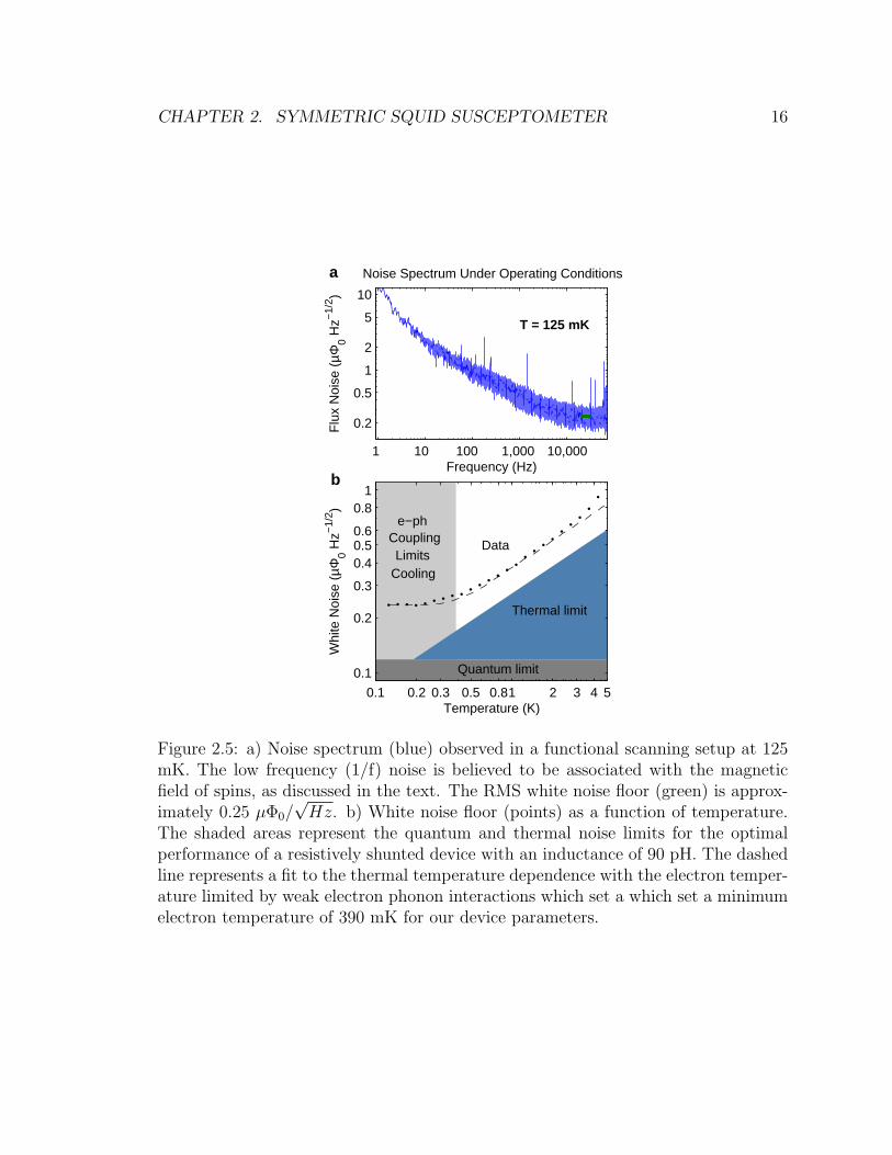
Figure 2.5: a) Noise spectrum (blue) observed in a functional scanning setup at 125mK. The low frequency (1/f) noise is believed to be associated with the magneticfield of spins, as discussed in the text. The RMS white noise floor (green) is approx-imately 0.25 µΦ0/
√Hz. b) White noise floor (points) as a function of temperature.
The shaded areas represent the quantum and thermal noise limits for the optimalperformance of a resistively shunted device with an inductance of 90 pH. The dashedline represents a fit to the thermal temperature dependence with the electron temper-ature limited by weak electron phonon interactions which set a which set a minimumelectron temperature of 390 mK for our device parameters.
CHAPTER 2. SYMMETRIC SQUID SUSCEPTOMETER 17
The 1/f-like low frequency noise is typically about 2 µΦ0/√Hz at 10 Hz, and
depends on frequency approximately as Φn ∝√SΦ = f−0.35 rather than
√SΦ = f−0.5
. We have checked that it does not come from the SQUID series array or room
temperature amplifier stages, and there is only very weak temperature dependence.
Tests using a bias reversal scheme [21] indicate that this low frequency noise is true
flux noise, rather than due to critical current fluctuations. Similar 1/f flux noise levels
have been reported for other devices [86].
2.4.2 Bandwidth
The bandwidth of the array with an open-circuit on the input coil is greater than
100 MHz. In closed-loop operation, the bandwidth is limited by the room temper-
ature electronics to approximately 5 MHz. In principle, the frequency response of
the susceptometer is limited by the L/R time-constant of the SQUID array input
inductance and susceptometer dynamic resistance. The measured bandwidth of the
present arrangement (1 MHz) is consistent with measured values of L and R.
2.5 Imaging and Coupling to Mesoscopic Samples
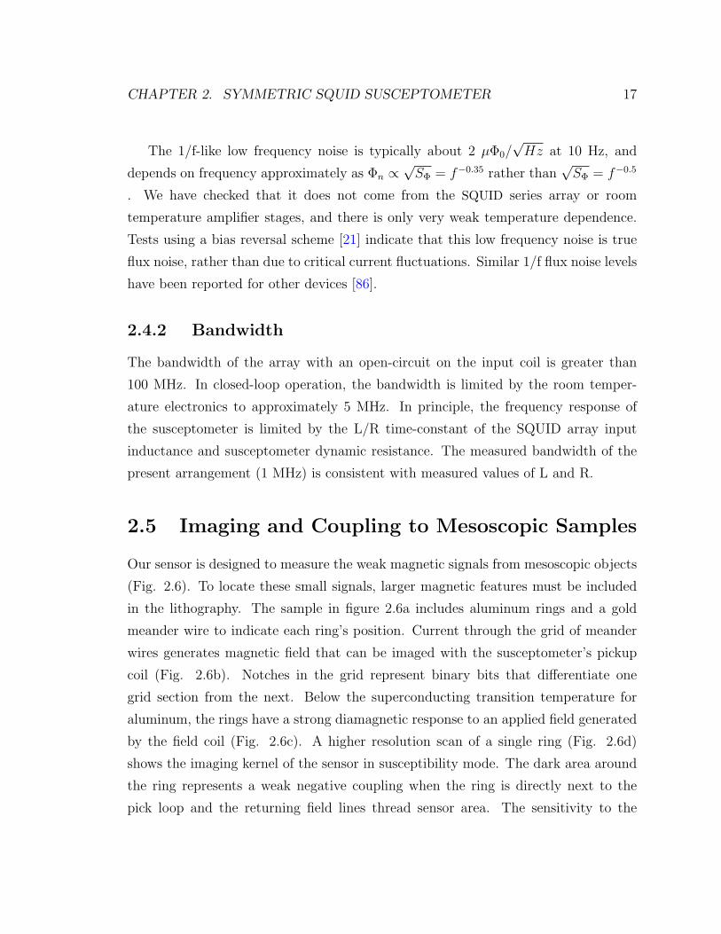
Our sensor is designed to measure the weak magnetic signals from mesoscopic objects
(Fig. 2.6). To locate these small signals, larger magnetic features must be included
in the lithography. The sample in figure 2.6a includes aluminum rings and a gold
meander wire to indicate each ring’s position. Current through the grid of meander
wires generates magnetic field that can be imaged with the susceptometer’s pickup
coil (Fig. 2.6b). Notches in the grid represent binary bits that differentiate one
grid section from the next. Below the superconducting transition temperature for
aluminum, the rings have a strong diamagnetic response to an applied field generated
by the field coil (Fig. 2.6c). A higher resolution scan of a single ring (Fig. 2.6d)
shows the imaging kernel of the sensor in susceptibility mode. The dark area around
the ring represents a weak negative coupling when the ring is directly next to the
pick loop and the returning field lines thread sensor area. The sensitivity to the
CHAPTER 2. SYMMETRIC SQUID SUSCEPTOMETER 18
Optical Image of Sample Magnetic Field from Gold Wire
30 µm
Susceptibility of a Ring
ab
c d
e f
20 µm
5 µm
30 µm
30 µm
Susceptibility of Rings
30 µm
Magnetic Field from a Vortex Low-T Susceptibility of Grid
-1
1
dΦ
dIGrid
(arb.)
SQ
-1
1
dΦ
dIFC
(arb.)
SQ
-1
1
dΦ
dIFC
(arb.)
SQ
-1
1
dΦ
dIFC
(arb.)
SQ
-1
1
Φ
(arb.)
SQ
Figure 2.6: (a) Optical micrograph of a sample with aluminum rings and a goldmeander wire. (b) Lockin measurement of current carried through the meander wire(different grid section). (c) Image of the rings’ superconducting response to fieldapplied from the field coils (susceptibility scan). (d) Higher resolution image of asingle ring showing the sensors imaging kernel in susceptibility mode. (e) Image of asingle superconducting vortex in niobium, demonstrating the magnetometry imagingkernel. (f) Susceptibility scan of the grid lines at ?? mK, which is consistent with a100 ppm? spin response.
CHAPTER 2. SYMMETRIC SQUID SUSCEPTOMETER 19
ring below the center of the scanned image represents flux threading the pickup loop
leads. The magnetometry response of a vortex pinned in niobium thin film sample
(Fig. 2.6e, zero applied field) represents typical response from a sharp feature with
its own intrinsic magnetic moment. The region where flux leaks through the pickup
loop leads represents a larger part of the “magnetometry kernal” as compared to the
susceptometry mode, because samples with intrinsic field source produce a measurable
signal outside of the area near the field coils. Figure 2.6f shows the response from a
sample like the one shown in 2.6a but where the superconducting (Al) rings have been
fabricated with normal metal (Au), and where a AlOx insulator exists above the grid
lines and below the rings. At the lowest temperatures (∼ 30 mK) a paramagnetic
susceptibility associated with spins in the metal and or this insulating layer[14] is
visible after averaging times of a few to several tens of minutes.
Once a scanning technique has been used to identify a specific sample on a multi-
sample substrate, the sensor can be used to make in situ background measurements,
allowing for the aquisition of a full I − Φ curve. This procedure involves measuring
the nonlinear SQUID response as a function of field (Fig. 2.7b) at various distances
from the sample in question (Fig. 2.7a). We usually apply a sinusoidal current to the
field coils in order to avoid high frequency components, which would be more affected
by the finite measurement bandwidth. The counter-wound design leads to the initial
two orders of magnitude of cancellation of the applied flux, as described above. After
nulling the linear in-phase component of this response by feeding an adjustable current
into the center tap, we typically find a residual signal on the order of 10−4 times the
bare applied flux. This residual signal consists mostly of an out-of-phase component,
which arises as the difference of two large signals of equal amplitude with a very
slight phase shift. Particularly at a large applied field, a nonlinear component that we
attribute to current induced pair breaking in or near the field coils becomes visible. To
distinguish this sensor background from the much smaller sample signal, we measure
it in situ by moving the pickup loop away from the sample and subtracting the result
from that obtained when coupled to the sample. Our best results were obtained when
moving the scanner on and off the sample parallel to the substrate, and measuring
about 1 s at each position, so that the background susceptibility from the substrate is
CHAPTER 2. SYMMETRIC SQUID SUSCEPTOMETER 20
−40 −20 0 20 40
−0.50
0.51
IFC
(mA)
−100
10
ΦS
Q (
µ Φ
0)
−2000
0
2000
a
dΦSQ
/dIFC
(µΦ0/mA)
b
c
d
−0.5
0
0.5
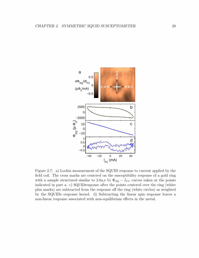
Figure 2.7: a) Lockin measurement of the SQUID response to current applied by thefield coil. The cross marks are centered on the susceptibility response of a gold ringwith a sample structured similar to 2.6a,e b) ΦSQ − IFC curves taken at the pointsindicated in part a. c) SQUIDresponse after the points centered over the ring (whiteplus marks) are subtracted from the response off the ring (white circles) as weightedby the SQUIDs response kernel. d) Subtracting the linear spin response leaves anon-linear response associated with non-equilibrium effects in the metal.
CHAPTER 2. SYMMETRIC SQUID SUSCEPTOMETER 21
also eliminated, and slow variations in the sensor background are averaged out. With
this procedure, we were able to obtain a nonlinear response of less than 0.1 µΦ0 at a
field coil current of 35 mA (corresponding to about 35 Φ0 or 35 G) after averaging for
38 hrs above a region of bare silicon substrate and subtracting the linear component.
The latter was at least partly due to the susceptibility of nearby metal patterned on
the substrate. Thus, we have achieved a cumulative background rejection of better
than 8.5 orders of magnitude.
2.6 Conclusion
We have characterized a Nb high-symmetry scanning SQUID susceptometer between
0.025 K and 6 K. The spectral density of the flux noise in the frequency-independent
region is 0.25 µΦ0/√Hz below ∼ 200 mK. This device has better than 100 times
greater spin sensitivity than our previous device, with more than 1000 times greater
bandwidth. The improved performance is due to the reduced sensor loop dimensions,
improved shielding, and improved symmetry with regard to the SQUID and field loop
placement, and voltage biasing techniques on the readout stage. As expected, the
limiting factor in bandwidth is set by the array input loop and the dynamic resistance
of the SQUID susceptometer. The ability to position the sensor over multiple samples
in a given cryogenic run and the ability to isolate the sensor from the samples for
background subtraction combine to maximize the device utility and sensitivity.
This work was supported by the Packard Foundation and by NSF Grants No.
DMR-0507931, DMR-0216470, ECS-0210877 and PHY-0425897. Some analysis was
supported by Stanford’s Center for Probing the Nanoscale (CPN), an NSF NSEC,
NSF Grant No. PHY-0425897. We thank J. R. Kirtley and K. Irwin for useful
discussions.
Chapter 3
A Terraced Scanning SQUID
Susceptometer with Sub-Micron
Pickup Loops
3.1 Our Sub-micron Terraced Susceptometers
Nicholas C. Koshnick, Martin E. Huber, Julie A. Bert, Clifford W. Hicks, Jeff Large,
Hal Edwards, Kathryn A. Moler
Applied Physics Letters, Dec 15, 2008 [50]
Abstract
SQUIDs can have excellent spin sensitivity depending on their magnetic flux noise,
pick-up loop diameter, and distance from the sample. We report a family of scanning
SQUID susceptometers with terraced tips that position the pick-up loops 300 nm
from the sample. The 600 nm – 2µm pickup loops, defined by focused ion beam, are
integrated into a 12-layer optical lithography process allowing flux-locked feedback,
in situ background subtraction and optimized flux noise. These features enable a
sensitivity of ∼70 electron spins per root Hertz at 4K.
22
CHAPTER 3. SUB-MICRON TERRACED SUSCEPTOMETER 23
In 1989, Ketchen et al.[45] argued that the advent of sub-micron lithography should
enable Superconducting Quantum Interference Devices (SQUIDs) with single electron
spin sensitivity. Stationary devices can measure nanomagnets with great success [88],
but it remains difficult, even with the highest spin-sensitivity SQUIDs [22], to detect
single-molecule field sources. Scanning devices [84, 46, 64, 32, 27, 37] make it possible
to isolate magnetic field sources and to perform background measurements in situ
[49]. Single-layer scanning nano-SQUIDs [32] have not yet achieved the excellent flux
sensitivity of the best large multi-layer SQUIDs. Multilayer SQUIDs thus far have
had large pickup areas that do not capture dipole field lines well thereby limiting the
spin sensitivity of these devices. For a normal-oriented dipole on the center line of a
pickup loop of radius R, the spin sensitivity, Sn, is
Sn(µB/√
Hz) = ΦnR
re
(1 +
h2
R2
)3/2
(3.1)
where Φn is the flux noise in units of Φ0/√
Hz, h is the pickup loop’s height above
the sample, and re = e2/mc2 ≈ 2.8× 10⁻¹⁵ m [45]. On the center line, near-optimal
signal is achieved for h < R. The spin sensitivity can be further improved by placing
the dipole near the edge of the pickup loop, although demagnetization limits this
enhancement for h < w, where w is the linewidth. For simplicity, we use Eq. 1 to
compare representative published scanning SQUIDs (Table 1).
Our scanning SQUID combines Focused Ion Beam (FIB) defined pick-up loops
with a 12 layer optical lithography process that includes local field coils. Integrated
terraces minimize h. We characterize the imaging kernel with a superconducting
vortex and a dipole field source. Flux noise measurements at 4 Kelvin demonstrate
a spin sensitivity of ∼70 µB/√
Hz. Flux noise may decrease at lower temperatures
(sections 2.4, 3.2) leading to a projected sensitivity of . 15 µB/√
Hz.
Our susceptometer incorporates two symmetric counter-wound arms, each with
an integrated modulation loop, pickup loop, and local field coil (Fig 1a). A three
metalization layer, linear coaxial transmission line geometry shields the device from
CHAPTER 3. SUB-MICRON TERRACED SUSCEPTOMETER 24
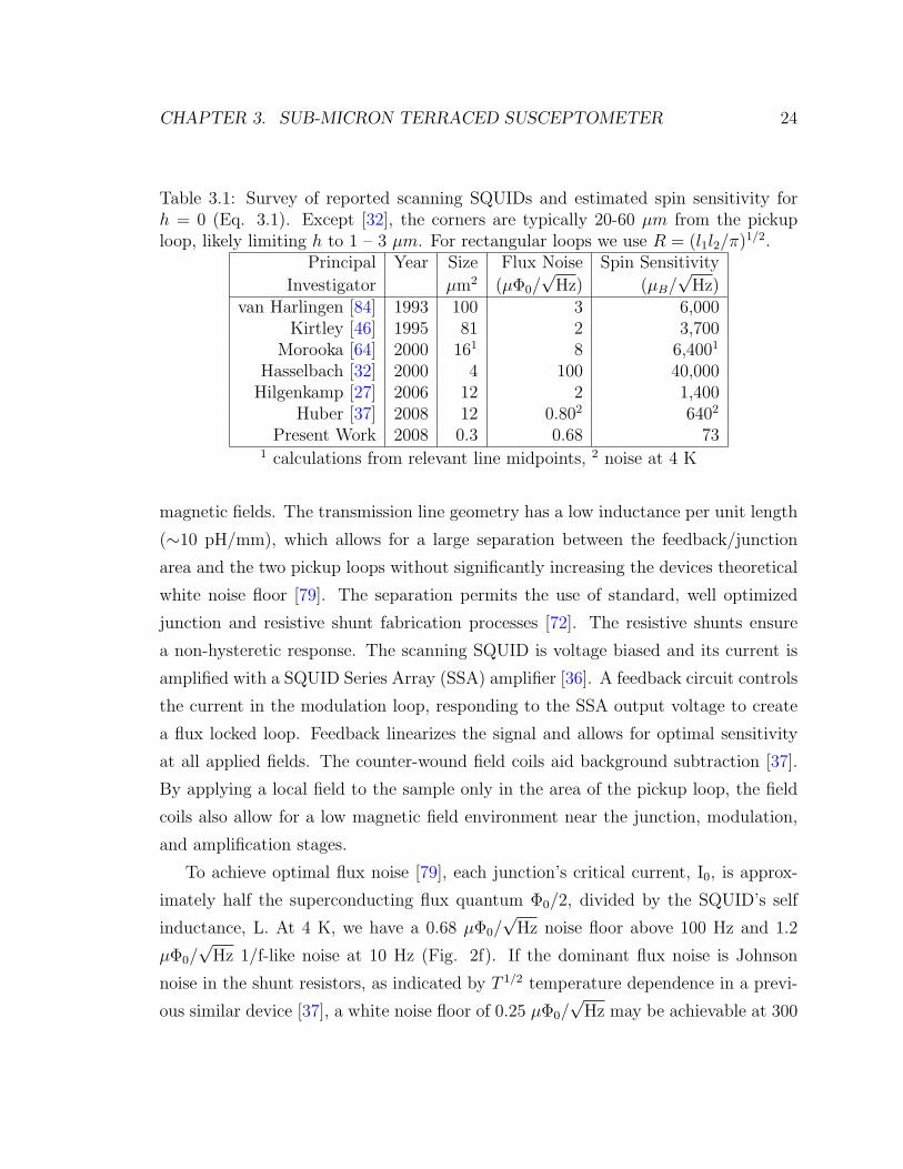
Table 3.1: Survey of reported scanning SQUIDs and estimated spin sensitivity forh = 0 (Eq. 3.1). Except [32], the corners are typically 20-60 µm from the pickuploop, likely limiting h to 1 – 3 µm. For rectangular loops we use R = (l1l2/π)1/2.
Principal Year Size Flux Noise Spin Sensitivity
Investigator µm2 (µΦ0/√
Hz) (µB/√
Hz)van Harlingen [84] 1993 100 3 6,000
Kirtley [46] 1995 81 2 3,700Morooka [64] 2000 161 8 6,4001
Hasselbach [32] 2000 4 100 40,000Hilgenkamp [27] 2006 12 2 1,400
Huber [37] 2008 12 0.802 6402
Present Work 2008 0.3 0.68 731 calculations from relevant line midpoints, 2 noise at 4 K
magnetic fields. The transmission line geometry has a low inductance per unit length
(∼10 pH/mm), which allows for a large separation between the feedback/junction
area and the two pickup loops without significantly increasing the devices theoretical
white noise floor [79]. The separation permits the use of standard, well optimized
junction and resistive shunt fabrication processes [72]. The resistive shunts ensure
a non-hysteretic response. The scanning SQUID is voltage biased and its current is
amplified with a SQUID Series Array (SSA) amplifier [36]. A feedback circuit controls
the current in the modulation loop, responding to the SSA output voltage to create
a flux locked loop. Feedback linearizes the signal and allows for optimal sensitivity
at all applied fields. The counter-wound field coils aid background subtraction [37].
By applying a local field to the sample only in the area of the pickup loop, the field
coils also allow for a low magnetic field environment near the junction, modulation,
and amplification stages.
To achieve optimal flux noise [79], each junction’s critical current, I0, is approx-
imately half the superconducting flux quantum Φ0/2, divided by the SQUID’s self
inductance, L. At 4 K, we have a 0.68 µΦ0/√
Hz noise floor above 100 Hz and 1.2
µΦ0/√
Hz 1/f-like noise at 10 Hz (Fig. 2f). If the dominant flux noise is Johnson
noise in the shunt resistors, as indicated by T 1/2 temperature dependence in a previ-
ous similar device [37], a white noise floor of 0.25 µΦ0/√
Hz may be achievable at 300
CHAPTER 3. SUB-MICRON TERRACED SUSCEPTOMETER 25
mK (see section 3.2). Cooling fins attached to the shunt resistors of some devices to
minimize the effect of electron-phonon coupling limited cooling may enable a white
noise floor of 0.12 µΦ0/√
Hz at dilution refrigerator temperatures (see section 3.2).
When limited by Johnson noise in resistive shunts, the theoretical flux noise de-
pendence scales like L3/2, whereas quantum noise scales like L1/2 [79]. The incentive
for a well quantified low inductance adds to the criteria for optimal pickup loop de-
sign. When the width, w, or the thickness, t, of a superconducting feature become
smaller than the penetration depth, λ, kinetic inductance can overcome the geomet-
rical inductance contribution [18] and scales like Lk ∝ λ2/wt [60]. Thus, linewidths
smaller than λ are undesirable. This effect, along with phase winding considerations
related to coherence length effects [31], ultimately sets the pickup loop size limit.
Inductance also scales with feature length, so we have kept the sub-micron portion of
the leads short, just long enough to allow the pickup loop to touch down first without
excessive stray pickup.
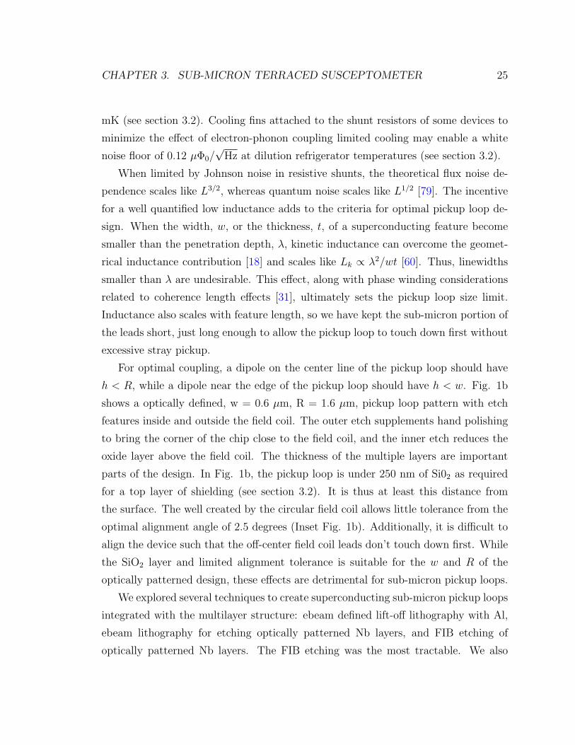
For optimal coupling, a dipole on the center line of the pickup loop should have
h < R, while a dipole near the edge of the pickup loop should have h < w. Fig. 1b
shows a optically defined, w = 0.6 µm, R = 1.6 µm, pickup loop pattern with etch
features inside and outside the field coil. The outer etch supplements hand polishing
to bring the corner of the chip close to the field coil, and the inner etch reduces the
oxide layer above the field coil. The thickness of the multiple layers are important
parts of the design. In Fig. 1b, the pickup loop is under 250 nm of Si02 as required
for a top layer of shielding (see section 3.2). It is thus at least this distance from
the surface. The well created by the circular field coil allows little tolerance from the
optimal alignment angle of 2.5 degrees (Inset Fig. 1b). Additionally, it is difficult to
align the device such that the off-center field coil leads don’t touch down first. While
the SiO2 layer and limited alignment tolerance is suitable for the w and R of the
optically patterned design, these effects are detrimental for sub-micron pickup loops.
We explored several techniques to create superconducting sub-micron pickup loops
integrated with the multilayer structure: ebeam defined lift-off lithography with Al,
ebeam lithography for etching optically patterned Nb layers, and FIB etching of
optically patterned Nb layers. The FIB etching was the most tractable. We also
CHAPTER 3. SUB-MICRON TERRACED SUSCEPTOMETER 26
5 µm−10 0 10
0
1 2.5°
µm
100
200
300
40020 µm
0 10 20
−0.5
0
0.5
1
µm
5° 2°
10 µm
a b
c d
pickup
loop
500nm500nm
Figure 3.1: a) Diagram of a counterwound SQUID susceptometer. Both the opticallypatterned tips (b) and FIB defined tips (c, d) feature etch defined terraces that reducethe pickup loop to sample distance. Figure b, inset: AFM data down the center lineof the device showing that the pickup loop is closest to the surface when the tip isaligned at precisely 2.5 degrees (more detail in section 3.2). In the FIB design (c), thethickness of the field coil and and pickup loop leads combine with the inner terraceto form a high centerline that allows roll angle tolerance. Figure c, inset: AFM datashowing the pickup loop can touch down first when the pitch angle is between 2-5.Pickup loops down to 600 nm can be reliably fabricated with a FIB defined etchprocess of the topmost layer.
found that sputtered Nb has a smaller penetration depth (∼90 nm) than e-beam
evaporated Al patterned with PMMA liftoff (∼120-160 nm), allowing for smaller
linewidths and reducing the calculated [40] inductance for a pair of pickup loops (22
pH vs. 66 pH). The inductance of the rest of the design is 60-65 pH. Here, we only
report results from optically and FIB defined Nb tips.
Our FIB design uses three superconducting layers (Fig 1c) such that the field coil
lines (gray) run underneath a shielding layer (purple) and approach the tip from the
same angle as the pickup loop. The pickup loop on the top layer (green) is closest to
the sample, which also allows for post-optical FIB processing. This design allows the
pickup loop to touch first when the SQUID is aligned to a pitch angle of 2 – 5(Fig.
CHAPTER 3. SUB-MICRON TERRACED SUSCEPTOMETER 27
1c inset), with a roll tolerance equal to the pitch angle.
To increase durability, we fabricated some devices with the pickup loop retracted
from the end of the etch-defined Si02 tab (Fig 1d), allowing the Si02 to take the
brunt of the wear. The Si02 tab also overlaps with the inside edge of the field coil,
making a high point that protects the pickup loop for pitch angles less than 2 degrees.
The alignment angle is difficult to set accurately and can change due to thermal
contractions, so these considerations are important for protecting the device.
10 µm
0.12Φ
0
dipole
1 µm
simulation
1 µm
vortex
1 µm
simulation
1 µm
−2 0 2
0
0.2
0.4
0.6
ΦS
Q (
Φ0)
section direction (µm)
vortex x
y
dipole
model
data
1 100 100000.1
1
10
Frequency (Hz)
µΦ
0/√
Hz
0.68
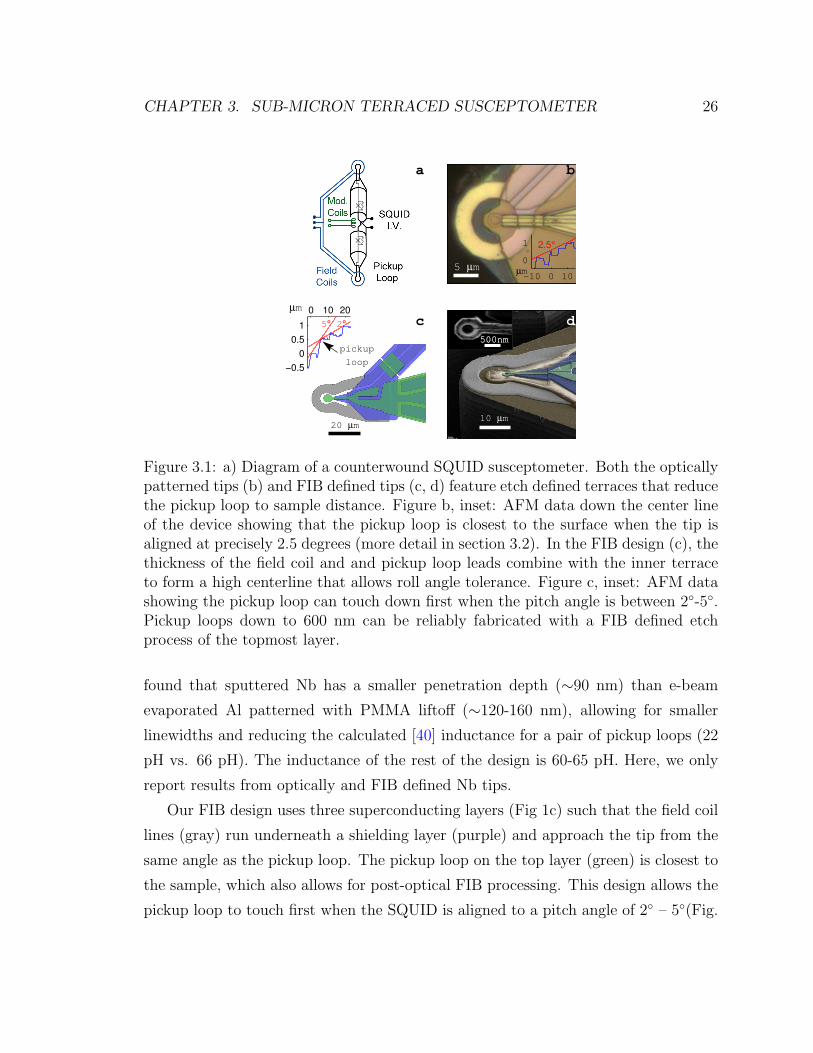
(a)(b) (c)
(d) (e)
(f)(g)
Figure 3.2: a) A FIB-fabricated device’s magnetometry response near an isolatedsuperconducting vortex. Both positive and negative flux coupling occurs near theleads to the pickup loop (shown on the right side). (b-f) data and modeled resultsfor a pickup loop with a 500 nm inner diameter and 250 nm linewidth. The fluxcaptured from an isolated surface dipole (b) and monopole magnetic field source (c)agrees with the modeled results (d,e) calculated by integrating the field lines thatthread a pickup loop kernal located 400 nm above the surface. (f) Linescans of (b-e)offset for clarity. (g) Noise spectrum at 4 K. The green line shows the rms averagebetween 5 KHz and 10 KHz.
We imaged Sr2RuO4 (Fig. 2) to characterize the FIB-defined device’s coupling
to a sample. Flux from a monopole-like superconducting vortex can couple through
both the pickup loop and its leads (Fig. 2a). Our smallest SQUIDs are designed
to do comparative studies on and off a particular mesoscopic structure, rather than
CHAPTER 3. SUB-MICRON TERRACED SUSCEPTOMETER 28
provide a point like imaging kernel.
Fitting a simple model of the pickup loop response to the vortex and dipole (Fig.
2b-g) gives an effective h. The vortex model is a monopole field source one penetration
depth (λSr2RuO4 = 150 nm) below the surface [46]. The dipole model is a free-space
dipole field source at the surface. The field from each of these two sources is integrated
over the effective pickup loop area at an effective height heff = 400 nm. This heff
implies that the closest side of the 200 nm thick pickup loop is 300 nm above the
scanned surface. Several effects could make this estimate of h larger than the physical
distance from the sample, such as the existence of a Meissner image dipole, λSr2RuO4 >
150 nm due to dead layers or finite T, and demagnetization effects from the thickness
of the pickup loop.
In conclusion, we have demonstrated SQUIDs with 0.68 µΦ0/√
Hz flux noise at
4 K, reliable FIB pickup loops with diameters as small as 600 nm, and a terraced
geometry that allows the pickup loop to come within 300 nm of the surface. These
features give a spin sensitivity of ∼70 µB/√
Hz, that is, the device noise is equivalent
to the signal from a single electron spin after an averaging time of a little more
than one hour. At lower temperatures a lower flux noise is likely, leading to spin
sensitivities less than 15µB/√
Hz.
3.2 Supplemental Material”
This section is also posed as EPAPS Document No. E-APPLAB-93-013850
(available at http://www.aip.org/pubservs/epaps.html).
This supplementary material explains the focused ion beam fabrication process, layer
thickness effects, and the possible effects of the shunt-resistor cooling fins.
CHAPTER 3. SUB-MICRON TERRACED SUSCEPTOMETER 29
3.2.1 FIB fabrication
The Focus Ion Beam (FIB) etch process was optimized at Texas Instruments circuit
design and repair lab with single beam (ion beam only) machines. The images shown
in Fig. 3.3 were taken at Stanford using a dual beam, SEM and ion beam, machine.
After etching, 15 of 17 devices continued to work with modulation depths and sym-
metry properties similar to their pre-tested values indicating no substantial change
in the devices’ inductance [67].
3.2.2 Layer Thickness Effects
Our fabrication steps did not include a planarization process between the various layer
depositions and etches. The geometric effects created by multiple layer crossings can
therefore be significant. We have used this to our advantage to optimize the touch
down properties of the tip as described in the main text and in Fig. 3.4a-d. The
graphical representation of the layers in b, d, and e do not demonstrate that the
etch-defined walls are not vertical. Therefore layers that appear to be discontinuous
in b and d are usually connected by material that extends over the side walls.
Because we did whole-wafer processing at NIST, we were not constrained to stan-
dard layer thicknesses or by the requirements of other devices. We processed two
wafers with the thicknesses listed in Table 3.2.
The values for wafer W46, shown in Fig. 3.4b, were chosen to further enhance the
alignment tolerance made possible by the new design. While this increase in the the
touchdown tolerance angle was not required, most of the FIB work was nevertheless
done on devices from this wafer because there was less over-etch on the W2 layer. This
left a comparatively wide pickup-loop-to-SQUID-body stem, which was easier to FIB
(ie. the process shown in Fig 3.3c). Conversely, most of the 3 and 4.6 µm SQUIDs
were from wafer W47. This was because many of the optically defined devices on
W46 lost their field coils during during an ultra-sound cleaning step.
The thicknesses for wafer W47 were used to construct Fig. 3.4d. The W47
thicknesses were chosen to be similar to the previous device [37] in order to reduce
the chance of open and short circuits that can occur at layer crossings. The one
CHAPTER 3. SUB-MICRON TERRACED SUSCEPTOMETER 30
5 µm 5 µm 5 µm
20 µm 20 µm
20 µm
2 µm 2 µm 2 µm
(a) (b) (c) (d)
(e) (f) (g) (h) (i)
Figure 3.3: Pickup loop structures were milled from an optically patterned Nb tab.(a) A FIB drilled hole creates the center of the pickup loop. (b) Successive stepsshape the outside of the pickup loop. (c) Leads are created by milling the center ofthe optically-defined stem, which connects the circular pickup loop to the rest of theSQUID. The pickup loop center is re-milled to remove redeposited material. (d) Thedevice chip is polished to a corner defined by an optically patterened trench, whichallows the active area of the device to touch first. (e,f) Before milling, a Pt strapis connected to the degenerately doped Si trench in order to increase the top layer’svisibility. This process allows the etch-stop point to be identified in situ while milling.The Pt strap is subsequently milled away. (g) SEM of a pickup loop that was milledin the presence of XeF2 gas to increase the etch rate and reduce the re-deposition.We found that this process continues to etch the Nb after the intended exposure overa period of many minutes. This effect is apparent in the distance between the innersquare, which represents the intended etch area, and the outer circle. This image alsoshows the result of over-etching the SiO2 layer, which leading to SiO2 peeling (bottomof inner square). To avoid wuch corrosive effects, later etches were done in withoutXeF2. (h) We could reliably make structures with line widths of ∼ 200 nm, limitedonly by Ga implantation effects [81] and the superconducting penetration depth.When compared to previous pickup loop structures that remain under oxide layers,these top layer structures show increased sensitivity to both mechanical contact (i)and electrostatic shock.
CHAPTER 3. SUB-MICRON TERRACED SUSCEPTOMETER 31
10 µm
0 10 20 30
−1
−0.5
0
0.5
1
µm
µm
5° 2°
S
−−BE
I1
−−W1
I2
−−−−−W2
5 µm
1 µm
−10 0 10 20−1.5
−1
−0.5
0
0.5
1
1.5
2.5°
µm
µm
−10 −5 0 5 10
−20
−10
0
10
20
IF.C.
(mA)
ΦSQUID (m
Φ0)
−10 0 10 20−1.5
−1
−0.5
0
0.5
1
µm
µm
(a) (b)
(c) (d)
(e)(f)
Figure 3.4: (a) Diagram of the three optically-defined superconducting layers beforethe final FIB milling step. (b) AFM data showing a cross section along the center lineof the SQUID with a graphical representation of the substrate (S), superconductinglayers (BE, W1, W2), and insulating layers (I1, I2) that create the steps. The layercrossings and etches are designed in such a way that the top layer pickup loop cantouch first if the alignment angle is between 2 and 5. (c) AFM data showing a 4.6µm optically defined SQUID with an etched terrace similar to the 3 µm discussed inthe main text. (d) AFM data and the corresponding layer diagram along the directionof one of the pickup loop leads. The pickup loop is closest to the sample when thedevice is aligned at an angle of 2.5. The top layer is used as a shield to make asmaller magnetometry imaging kernel. When imaging items of the pickup loops 4.6µm size, the increased scan height caused by the lack of alignment tolerance, andburied (middle layer) pickup loop is not significant. Therefore this device is welloptimized for imaging micron scale samples. (e) SQUID response as a function offield coil current in a 3 µm device. Flux jumps reproducibly occur at certain valuesof IF.C.. (f) Diagram demonstrating how a 200 nm base electrode layer (as used inprevious devices [37]) allows for more contiguous upper wiring layers, as compared tothe 300 nm base electrode line (b,c) used in this generation of devices.
CHAPTER 3. SUB-MICRON TERRACED SUSCEPTOMETER 32
Table 3.2: Layer thicknesses of the two processed wafers.Wafer Counter Base Resistors Insulator Wiring Insulator Wiring
Electrode Electrode one one two two(CE) (BE) (I1) (W1) (I2) (W2)
W46 120 nm 300 nm 150 nm 425 nm 180 nm 330 nm 200W47 120 nm 300 nm 150 nm 350 nm 230 nm 350 nm 250
exception was that the base electrode thickness was increased from 200 to 300 nm to
help increase the maximum field coil current, ImaxF.C. . The width of the field coil lines
was also increased. While these changes allowed ImaxF.C. to increase from ∼ 75 mA to
∼ 135 mA, the current where vortices begin move, IvjumpF.C. , went from ∼ 45 mA to
as little as 6 mA (Fig. 3.4e). Above ±13 mA, the vorticies jump at irregular field
values, making the careful comparison of magnetization curves between two points
on or off the sample difficult. To the extent that precise magnetization curves [49]
are an important design goal, future design improvements should focus on increasing
IvjumpF.C. rather than ImaxF.C. . While many effects can cause a low IvjumpF.C. , we expect the
reduced value may be caused by discontinuities created by the 300 nm base electrode
layer, as portrayed by the difference between Fig. 3.4d and Fig. 3.4f. The value of
IvjumpF.C. was similar for both W46 and W47.
3.2.3 Cooling fins
As discussed in the main text, the dominant noise source in our design is expected
to be Johnson noise in the shunt resistors. At low temperatures Joule heating from
the SQUID bias current can saturate the electron temperature of the resistors, and
thereby saturate the device’s white noise floor above the quantum and the thermal
limits. In this case, cooling is most likely limited by the relatively weak electron-
phonon coupling interactions [85]. To address this potential limitation, we have added
cooling fins to our shunt resistors to increase the volume where electron-phonon in-
teractions can occur, Fig. 3.5a. The cooling fins increase the normal electron volume
by more than a factor of one thousand allowing the minimum theoretical electron
temperature to go from 392 mK to 135 mK, Fig. 3.5b.
CHAPTER 3. SUB-MICRON TERRACED SUSCEPTOMETER 33
60 µm
Cooling Fin
Temperature (K)
Whi
te N
oise
(µΦ
0/Hz1/
2 )
JohnsonNoise Limit
Quantum Noise Limit
e−ph
Lim
it W
ith F
ins
e−ph
Coo
ling
Lim
it w
/o F
ins 4.6 µm device
FIB device
0.1 0.20.3 0.5 0.81 2 3 4 5
0.1
0.2
0.3
0.40.50.6
0.81(a) (b)
Shunt Resistor J. Junction
Mod Coils
Figure 3.5: (a) An optical micrograph of the SQUID core, which includes Josephsonjunctions, shunt resistors, and modulation coils. The design improves on our previouswork [37] by adding cooling fins to help dissipate the heat generated in the shuntresistors by increasing the volume where electrons and phonons can thermalize. (b)A reproduction of the white noise of an earlier device [37] as a function of temperature,and the 0.68 µΦ0/
√Hz noise from one current generation device at 4.2K. The lower
right shaded areas represent the Johnson and quantum noise limits [79], given therelevant device parameters. The left hand shaded areas indicate the e-ph limitedcooling limits with and without cooling fins when a 1.2 Ω shunt resistor is heated by9 µA of current.
CHAPTER 3. SUB-MICRON TERRACED SUSCEPTOMETER 34
The cooling fins must be well coupled to the shunt resistors so that thermal gra-
dients do not limit the desired effect. One can obtain a back-of-the-envelope estimate
for such a gradient by using the Wiedeman-Franz law. From this law at a base tem-
perature of 0.1K, 200 pW of power in a resistor (10 µA through 2 Ω) generates a
thermal gradient of ∼ 0.1K when the resistance between the shunt resistor and the
main part of the cooling fin, Rc, is 1Ω. This gradient scales approximately linearly
with Rc. The shunt resistors were designed to be less than 0.5 squares away from to
the cooling fins in order to make the thermal gradient less than 0.1 K. Both the resis-
tors and the cooling fins are made from a PdAu layer with R∼ 2Ω. The cooling fins
were fabricated directly on top of the silicon wafer to maximize thermal conductivity
to the substrate.
Chapter 4
Fluctuation Induced
Superconductivity in Mesoscopic
Aluminum Rings
4.1 Fluctuation Superconductivity in Mesoscopic
Aluminum Rings
Nicholas C. Koshnick, Hendrik Bluhm, Martin E. Huber, Kathryn A. Moler,
From Science, 318, 1440-1443 (2007)
Reprinted with permission from AAAS.
Modified slightly to use the available space for clarity.
Abstract
Fluctuations are important near phase transitions, where they can be difficult to de-
scribe quantitatively. Superconductivity in mesoscopic rings is particularly intriguing
because the critical temperature is an oscillatory function of magnetic field. There
is an exact theory for thermal fluctuations in one-dimensional superconducting rings,
which are therefore expected to be an excellent model system. We measure the sus-
ceptibility of many rings, one ring at a time, using a scanning SQUID that can isolate
35
CHAPTER 4. FLUCTUATION SUPERCONDUCTIVITY IN RINGS 36
magnetic signals from seven orders of magnitude larger background applied flux. We
find that the fluctuation theory describes the results and that a single parameter
characterizes the ways in which the fluctuations are especially important at magnetic
fields where the critical temperature is suppressed.
Superconductivity requires both electron pairing and the coalescence of the pairs
into a macroscopic quantum state with long-range phase coherence, usually described
as a single wavefunction. In restricted geometries, thermal energy allows contribu-
tions from multiple wavefunctions to dramatically change the behavior of the system
[26, 51, 53]. Experimental knowledge of fluctuations in 1D is largely derived from
transport measurements [55], which can alter the state of a mesoscopic sample: gen-
erating measurable voltages may induce non-equilibrium dynamics, and leads on the
sample introduce proximity effects over the length scale of the temperature-dependent
Ginzburg-Lanau (G-L) coherence length, ξ. We use a contact-less technique to study
isolated, quasi-1D rings with a contact-less technique that allows us to measure fluc-
tuation effects on length scales that are comparable to and smaller than ξ(T ).
Using a scanning micro-Superconducting QUantum Interference Device (SQUID),
we detect the persistent currents in many quasi-1D aluminum rings, one ring at a time,
paying particular attention to small currents near each ring’s superconducting tran-
sition temperature, Tc. Although the magnetic signals are small, such measurements
have many advantages in principle. In 1D, the current about a ring, I, is related to
the free energy, F , via I = −∂F/∂Φa, where Φa is the flux threaded through the
ring by an applied magnetic field. Measuring I as a function of Φa thus allows us
to test a fundamental thermodynamic variable and our understanding of the ring’s
state. If the superconducting condensate is coherent about the ring’s circumference
L, the ring’s current near zero applied field is proportional to the density of pairs.
Deviations from such mean field solutions provide information about amplitude and
phase fluctuations in the ring. Because the kinetic energy is related to the applied
flux, it can be tuned externally, which can lead to additional fluctuation effects.
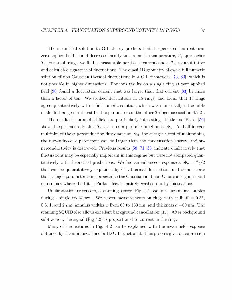
CHAPTER 4. FLUCTUATION SUPERCONDUCTIVITY IN RINGS 37
The mean field solution to G-L theory predicts that the persistent current near
zero applied field should decrease linearly to zero as the temperature, T , approaches
Tc. For small rings, we find a measurable persistent current above Tc, a quantitative
and calculable signature of fluctuations. The quasi-1D geometry allows a full numeric
solution of non-Gaussian thermal fluctuations in a G-L framework [73, 83], which is
not possible in higher dimensions. Previous results on a single ring at zero applied
field [90] found a fluctuation current that was larger than that current [83] by more
than a factor of ten. We studied fluctuations in 15 rings, and found that 13 rings
agree quantitatively with a full numeric solution, which was numerically intractable
in the full range of interest for the parameters of the other 2 rings (see section 4.2.2).
The results in an applied field are particularly interesting. Little and Parks [56]
showed experimentally that Tc varies as a periodic function of Φa. At half-integer
multiples of the superconducting flux quantum, Φ0, the energetic cost of maintaining
the flux-induced supercurrent can be larger than the condensation energy, and su-
perconductivity is destroyed. Previous results [58, 71, 33] indicate qualitatively that
fluctuations may be especially important in this regime but were not compared quan-
titatively with theoretical predictions. We find an enhanced response at Φa = Φ0/2
that can be quantitatively explained by G-L thermal fluctuations and demonstrate
that a single parameter can characterize the Gaussian and non-Gaussian regimes, and
determines where the Little-Parks effect is entirely washed out by fluctuations.
Unlike stationary sensors, a scanning sensor (Fig. 4.1) can measure many samples
during a single cool-down. We report measurements on rings with radii R = 0.35,
0.5, 1, and 2 µm, annulus widths w from 65 to 180 nm, and thickness d =60 nm. The
scanning SQUID also allows excellent background cancellation (12). After background
subtraction, the signal (Fig 4.2) is proportional to current in the ring.
Many of the features in Fig. 4.2 can be explained with the mean field response
obtained by the minimization of a 1D G-L functional. This process gives an expression
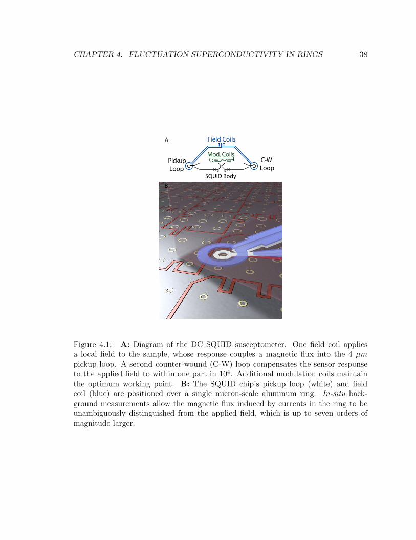
CHAPTER 4. FLUCTUATION SUPERCONDUCTIVITY IN RINGS 38
Field Coils
Mod. Coils
SQUID Body
A
B
Pickup Loop
C-W Loop
Figure 4.1: A: Diagram of the DC SQUID susceptometer. One field coil appliesa local field to the sample, whose response couples a magnetic flux into the 4 µmpickup loop. A second counter-wound (C-W) loop compensates the sensor responseto the applied field to within one part in 104. Additional modulation coils maintainthe optimum working point. B: The SQUID chip’s pickup loop (white) and fieldcoil (blue) are positioned over a single micron-scale aluminum ring. In-situ back-ground measurements allow the magnetic flux induced by currents in the ring to beunambiguously distinguished from the applied field, which is up to seven orders ofmagnitude larger.
CHAPTER 4. FLUCTUATION SUPERCONDUCTIVITY IN RINGS 39
−5
0
5 C
−0.1
0
0.11.22K 1.245K
1.257K
−50
0
50 B
ΦS
QU
ID (
µΦ0)
−1
0
11.22K1.23K
1.236K
I ring (
µA)
−200
0
200 A
−5
0
51.18K1.20K
1.22K
−0.5 −0.25 0 0.25 0.5
−100
0
100D
ΦS
QU
ID (
µΦ0)
Applied Flux (Φ0)
−0.1
0
0.11.245K
1.25K
I ring (
µA)
−1 0 1
−7575
−202 1.255K
Figure 4.2: SQUID signal (left axis) and ring current (right axis) as a function ofapplied flux Φa for two rings, both with thickness d = 60 nm and width w = 110 nm.The fluctuation theory (dashed red) was fit to the data (blue) through the temperatureanalysis shown in Fig 4.3. A-C Radius R = 0.35 µm, fitted Tc(Φa = 0) = 1.247 K,and γ = 0.075. The green dashed line is the theoretical mean-field response forT = 1.22K and shows the characteristic Little-Parks lineshape, in which the ring isnot superconducting near Φa = Φ0/2. The excess persistent current in this regionindicates the large fluctuations in the Little-Parks regime. D Radius R = 2 µm, fittedTc = 1.252 K, and γ = 13. The periodic response (right inset) shows a 1D treatmentis appropriate and can be approximated by a thermal average over mean field G-Lfluxoid states (eq. 4.2 and section 4.2) until addition fluctuations contribute near Tc.
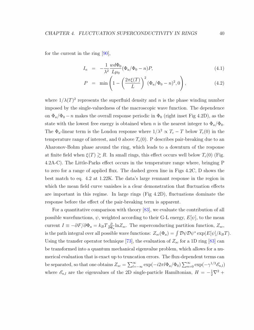
CHAPTER 4. FLUCTUATION SUPERCONDUCTIVITY IN RINGS 40
for the current in the ring [90],
In = − 1
λ2
wdΦ0
Lµ0
(Φa/Φ0 − n)P, (4.1)
P = min
(1−
(2πξ(T )
L
)2
(Φa/Φ0 − n)2, 0
), (4.2)
where 1/λ(T )2 represents the superfluid density and n is the phase winding number
imposed by the single-valuedness of the macroscopic wave function. The dependence
on Φa/Φ0−n makes the overall response periodic in Φ0 (right inset Fig 4.2D), as the
state with the lowest free energy is obtained when n is the nearest integer to Φa/Φ0.
The Φa-linear term is the London response where 1/λ2 ∝ Tc − T below Tc(0) in the
temperature range of interest, and 0 above Tc(0). P describes pair-breaking due to an
Aharonov-Bohm phase around the ring, which leads to a downturn of the response
at finite field when ξ(T ) & R. In small rings, this effect occurs well below Tc(0) (Fig.
4.2A-C). The Little-Parks effect occurs in the temperature range where, bringing P
to zero for a range of applied flux. The dashed green line in Figs 4.2C, D shows the
best match to eq. 4.2 at 1.22K. The data’s large remnant response in the region in
which the mean field curve vanishes is a clear demonstration that fluctuation effects
are important in this regime. In large rings (Fig 4.2D), fluctuations dominate the
response before the effect of the pair-breaking term is apparent.
For a quantitative comparison with theory [83], we evaluate the contribution of all
possible wavefunctions, ψ, weighted according to their G-L energy, E[ψ], to the mean
current I ≡ −∂F/∂Φa = kBT∂∂Φa
lnZsc. The superconducting partition function, Zsc,
is the path integral over all possible wave functions: Zsc(Φa) =∫DψDψ∗ exp(E[ψ]/kBT ).
Using the transfer operator technique [73], the evaluation of Zsc for a 1D ring [83] can
be transformed into a quantum mechanical eigenvalue problem, which allows for a nu-
merical evaluation that is exact up to truncation errors. The flux-dependent terms can
be separated, so that one obtains Zsc =∑∞
l=−∞ exp(−i2πlΦa/Φ0)∑∞
n=0 exp(−γ1/3En,l)
where En,l are the eigenvalues of the 2D single-particle Hamiltonian, H = −12∇2 +
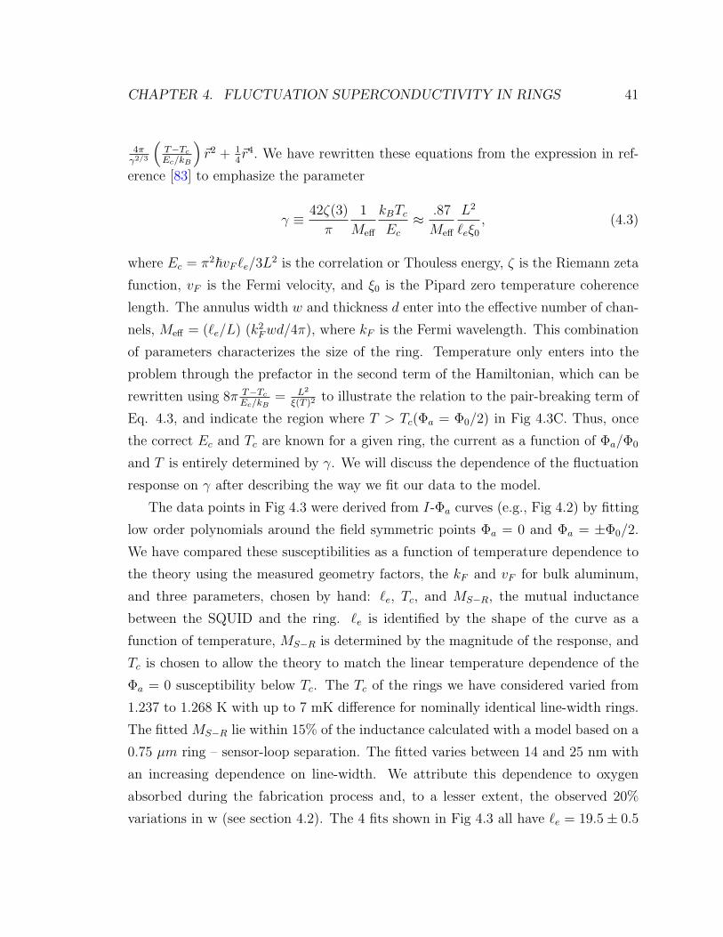
CHAPTER 4. FLUCTUATION SUPERCONDUCTIVITY IN RINGS 41
4πγ2/3
(T−Tc
Ec/kB
)~r2 + 1
4~r4. We have rewritten these equations from the expression in ref-
erence [83] to emphasize the parameter
γ ≡ 42ζ(3)
π
1
Meff
kBTcEc≈ .87
Meff
L2
`eξ0
, (4.3)
where Ec = π2~vF `e/3L2 is the correlation or Thouless energy, ζ is the Riemann zeta
function, vF is the Fermi velocity, and ξ0 is the Pipard zero temperature coherence
length. The annulus width w and thickness d enter into the effective number of chan-
nels, Meff = (`e/L) (k2Fwd/4π), where kF is the Fermi wavelength. This combination
of parameters characterizes the size of the ring. Temperature only enters into the
problem through the prefactor in the second term of the Hamiltonian, which can be
rewritten using 8π T−Tc
Ec/kB= L2
ξ(T )2 to illustrate the relation to the pair-breaking term of
Eq. 4.3, and indicate the region where T > Tc(Φa = Φ0/2) in Fig 4.3C. Thus, once
the correct Ec and Tc are known for a given ring, the current as a function of Φa/Φ0
and T is entirely determined by γ. We will discuss the dependence of the fluctuation
response on γ after describing the way we fit our data to the model.
The data points in Fig 4.3 were derived from I-Φa curves (e.g., Fig 4.2) by fitting
low order polynomials around the field symmetric points Φa = 0 and Φa = ±Φ0/2.
We have compared these susceptibilities as a function of temperature dependence to
the theory using the measured geometry factors, the kF and vF for bulk aluminum,
and three parameters, chosen by hand: `e, Tc, and MS−R, the mutual inductance
between the SQUID and the ring. `e is identified by the shape of the curve as a
function of temperature, MS−R is determined by the magnitude of the response, and
Tc is chosen to allow the theory to match the linear temperature dependence of the
Φa = 0 susceptibility below Tc. The Tc of the rings we have considered varied from
1.237 to 1.268 K with up to 7 mK difference for nominally identical line-width rings.
The fitted MS−R lie within 15% of the inductance calculated with a model based on a
0.75 µm ring – sensor-loop separation. The fitted varies between 14 and 25 nm with
an increasing dependence on line-width. We attribute this dependence to oxygen
absorbed during the fabrication process and, to a lesser extent, the observed 20%
variations in w (see section 4.2). The 4 fits shown in Fig 4.3 all have `e = 19.5± 0.5
CHAPTER 4. FLUCTUATION SUPERCONDUCTIVITY IN RINGS 42
1.18 1.2 1.22 1.24 1.26
−4
−2
0
2A
dI/d
Φa (
µA/Φ
0)
T (K)
Φa= 0
Φa=
Φ0__
2
1 1.01 1.020
0.2
0.4
0.6
0.8
B
1/λ ef
f2
(µm
−2 )
T/Tc (K)
Φa= 0
R = .35 µm
R = .5 µm
R = 1 µm
R = 2 µm
C
dI/d
Φa (
µA/Φ
0)
8kB(T−T
c(0))/πE
c = ± (2R/ξ(T))2
γ = 13
γ = 1.6
γ = 0.22 γ = 0.075
Φa= 0
Φa=
Φ0__
2
−1 −0.5 0 0.5
−2
−1
0
1
Figure 4.3: Susceptibility data (symbols) and fits (lines) at Φa = 0 (positive values)and Φ0/2 (negative values) for 110 nm wide 60 nm thick rings with various radii,R. A Smaller rings have a larger temperature region where the Little-Parks criterionξ(T ) > 2R is satisfied, and thus have a larger region with a reduced Φa = Φ0/2response. B Φa = 0 susceptibility scaled with the cross section and radius to showthe effective mean field superfluid density around Tc. Smaller rings have an enhancedfluctuation response. C When the temperature is scaled by the correlation energyEc, the susceptibility is uniquely determined by the size parameter γ. The greyand green shaded regions indicate the temperature above Tc(Φa) for Φ = 0 andΦ0/2, respectively. The fluctuation response above Tc(Φa) is clearly enhanced forΦa = Φ0/2. The dotted line shows a Gaussian prediction (see section 4.2) that isvalid at some γ-dependent temperature above Tc(Φa). When γ & 1, the response atΦa = 0 and Φ0/2 are comparable in the Little-Parks regime, which corresponds to afluctuation dominated sinusoidal I − Φa response.
CHAPTER 4. FLUCTUATION SUPERCONDUCTIVITY IN RINGS 43
nm. The agreement with the 1D models we have discussed demonstrates that the
finite line-width effects are not essential to our physical result and that small variations
in w do not qualitatively change the response above Tc(Φa).
Near Tc(Φa), γ characterizes the non-Gaussian fluctuations that interpolate be-
tween the mean field behavior far below Tc and the Gaussian fluctuations that domi-
nate at high temperatures. Non-Gaussian fluctuations are important when quadratic
expansions of the free energy cannot describe the physical result. This is particularly
apparent at Tc(Φa), where any Gaussian approximation would predict a divergent sus-
ceptibility [3]. By using Eq 4.2 to define an effective superfluid density from the zero
field response, 1λ2
eff= µ0L
wd∂I∂Φa
∣∣Φa=0
, one can see (Fig 4.3B) that fluctuations make the
susceptibility deviate from the mean field response below Tc(0), gradually smoothing
the transition. Our parameterization of the theory shows that γ is the only sample
dependent parameter at T = Tc(0). The temperature range where non-Gaussian fluc-
tuations are important is typically parameterized through the Ginzburg parameter as
|T−Tc(Φa)|/Tc < Gi, or equivalently |T−Tc(Φa)|/Ec < 2π2
√γ = Tc
EcGi [25, 75]. Inside
this range, γ determines the magnitude of the response. Far above this range, Gaus-
sian fluctuations dominate and the susceptibility is a function of |T −Tc|/Ec ∝ L2/ξ2
alone.
The theory’s dependence on γ allows us to state the criterion for the visibility of the
Little-Parks effect in the context of fluctuations. The region that is shaded in green
in Fig 4.3C is above Tc(Φa = Φ0/2) because ξ(T ) > L/π. The susceptibility would
be zero in this regime if fluctuation effects were not considered. When γ 1, the
distinct Little-Parks shape is visible, in that the susceptibility is smaller at Φa = Φ0/2
than at Φa = 0. However, when γ 1, the Little-Parks shape is entirely washed out
by fluctuations (Fig 4.4). For sufficiently large γ, the susceptibilities at Φ = 0 and
Φ0/2 are equal and opposite even below Tc(Φ = 12) so the response appears sinusoidal.
This dependence on γ, rather than L and ξ alone, is the reason why the Little-Parks
lineshape does not occur in the ring shown in Fig 4.2A, 4.4C.
Several factors contribute to the large fluctuation response near Φa = Φ0/2 above
Tc(Φa). First, the Gaussian fluctuations between Tc(Φa = 0) and Tc(Φa) have an large
magnitude which is due to the interplay between adjacent phase winding states. In
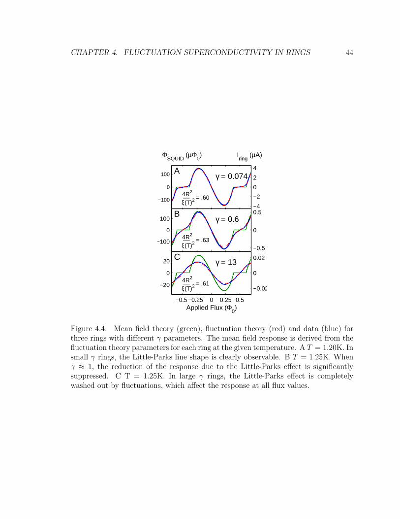
CHAPTER 4. FLUCTUATION SUPERCONDUCTIVITY IN RINGS 44
−0.5−0.25 0 0.25 0.5
−20
0
20
Applied Flux (Φ0)
−0.02
0
0.02
−100
0
100
−0.5
0
0.5
−100
0
100
−4
−2
0
2
4
ΦSQUID
(µΦ0) I
ring (µA)
A
B
C
4R2
4R2
4R2
__
__
__
ξ(T)2
ξ(T)2
ξ(T)2
= .60
= .63
= .61
γ = 0.074
γ = 0.6
γ = 13
Figure 4.4: Mean field theory (green), fluctuation theory (red) and data (blue) forthree rings with different γ parameters. The mean field response is derived from thefluctuation theory parameters for each ring at the given temperature. A T = 1.20K. Insmall γ rings, the Little-Parks line shape is clearly observable. B T = 1.25K. Whenγ ≈ 1, the reduction of the response due to the Little-Parks effect is significantlysuppressed. C T = 1.25K. In large γ rings, the Little-Parks effect is completelywashed out by fluctuations, which affect the response at all flux values.
CHAPTER 4. FLUCTUATION SUPERCONDUCTIVITY IN RINGS 45
small γ rings, the non-Gaussian fluctuation region in Fig 4.3C is quite small. Thus,
there is a large region where the magnitude of the persistent current near Φ = Φ0/2
is strictly a function of kB(T − Tc)/Ec. In large γ rings, non-Gaussian fluctuations
play an increased role in the phase diagram, multiple phase winding modes need to
be considered [25] indicating the importance of phase fluctuations. In all rings, non-
homogeneous wavefunction solutions similar to saddle points solutions may have a
non-negligible contribution to the final currents due to their vanishing energy cost
near Tc(Φa). Small variations in width 4.2 make non-homogeneous wavefunctions
more important [9], and would be important to include in an extended theory.
Fluctuation effects play a important role in 1D superconducting structures. Our
analysis explicitly demonstrates how Gaussian and non-Gaussian fluctuations affect
the persistent current in rings with various diameters and cross-sections, as a function
of applied magnetic flux. A single parameter, γ, characterizes the fluctuations for
a given ratio of the temperature-dependent coherence length to the circumference.
When γ is large, the signature of a Little-Parks flux dependent Tc(Φa) is entirely
washed out by fluctuations. When γ is small, the susceptibility in the non-Gaussian
region near Tc(Φa) is enhanced and Gaussian fluctuations are clearly visible between
Tc(Φa) and Tc(0) for Φa ≈ Φ0/2. This new framework for understanding Little-Parks
fluctuations is supported by our data on fluctuation-induced currents in rings.
4.2 Supplementary Online Material for
“”Fluctuation Superconductivity in Mesoscopic
Aluminum Rings”
Abstract
In the materials and methods section, this document elaborates on the experimen-
tal Superconducting Quantum Interference Device (SQUID) technique introduced in
section 4.1 by describing the measurement apparatus and experimental conditions.
After describing the sample fabrication, special attention is given to variations in the
CHAPTER 4. FLUCTUATION SUPERCONDUCTIVITY IN RINGS 46
cross section of the ring, which can have the effect of a decreased mean free path.
The supporting online text section expands theoretical discussion, pedagogically in-
troducing the Ginzburg Landau (G-L) free energy and the effects one might expect
in finite line-width rings. The discussion includes a fluxoid fluctuation model that is
appropriate far below Tc(Φ) and a Gaussian fluctuation model that is appropriate far
above Tc(Φ). The section concludes by describing aspects of the full fluctuation solu-
tion discussed in the main text such as the difficulties involved with its full numeric
solution far from Tc(0). Two tables introduce the measured and fitted parameters for
each ring, and the agreement with a quantitative SQUID–Ring mutual inductance
model. Additional data of each ring’s response as a function of temperature at three
flux values is available online.
4.2.1 Materials and Methods
Our measurement apparatus [11] consists of a SQUID susceptometer attached to a
scanning assembly that includes a large area scanner and an atto-cube coarse posi-
tioner system. Sub-millikelvin temperature control is made possible by feeding back
on the temperature of the sample/scanner assembly, which is connected to the base
plate of a dilution refrigerator through a single copper braid. The primary evidence
for the fact that thermal drifts within the system do not significantly affect this
control mechanism is that ring-current features, which vary strongly with tempera-
ture, change by less than 1 mK after a period of up to several days regardless of the
temperature state before the measurement was made.
The DC SQUID susceptometer is voltage-biased and amplified by a series-array
SQUID preamplifier [36]. Feedback through integrated modulation coils allows for
optimal noise performance and a linearized response at all applied fields. Under
operating conditions, the susceptometer has a 1/f noise of ∼ 2 µΦ0/√
Hz around the
measurement frequency of 10 Hz. This low frequency noise is similar to the reported
noise of other devices [86]. Additional measurements indicate that this low frequency
noise is not due to the room temperature electronics or any of the amplification stages.
Tests using bias reversal schemes [21] indicate that this noise is flux noise, rather
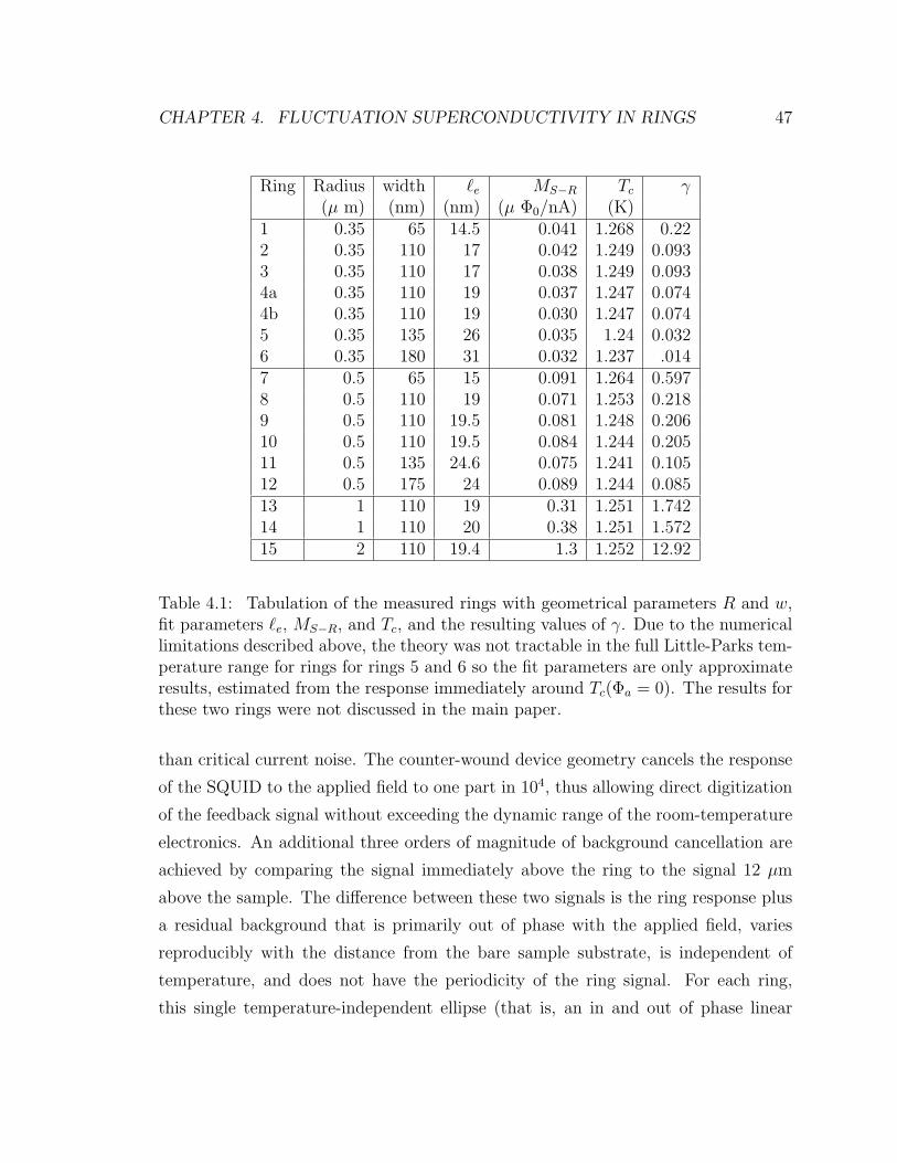
CHAPTER 4. FLUCTUATION SUPERCONDUCTIVITY IN RINGS 47
Ring Radius width `e MS−R Tc γ(µ m) (nm) (nm) (µ Φ0/nA) (K)
1 0.35 65 14.5 0.041 1.268 0.222 0.35 110 17 0.042 1.249 0.0933 0.35 110 17 0.038 1.249 0.0934a 0.35 110 19 0.037 1.247 0.0744b 0.35 110 19 0.030 1.247 0.0745 0.35 135 26 0.035 1.24 0.0326 0.35 180 31 0.032 1.237 .0147 0.5 65 15 0.091 1.264 0.5978 0.5 110 19 0.071 1.253 0.2189 0.5 110 19.5 0.081 1.248 0.20610 0.5 110 19.5 0.084 1.244 0.20511 0.5 135 24.6 0.075 1.241 0.10512 0.5 175 24 0.089 1.244 0.08513 1 110 19 0.31 1.251 1.74214 1 110 20 0.38 1.251 1.57215 2 110 19.4 1.3 1.252 12.92
Table 4.1: Tabulation of the measured rings with geometrical parameters R and w,fit parameters `e, MS−R, and Tc, and the resulting values of γ. Due to the numericallimitations described above, the theory was not tractable in the full Little-Parks tem-perature range for rings for rings 5 and 6 so the fit parameters are only approximateresults, estimated from the response immediately around Tc(Φa = 0). The results forthese two rings were not discussed in the main paper.
than critical current noise. The counter-wound device geometry cancels the response
of the SQUID to the applied field to one part in 104, thus allowing direct digitization
of the feedback signal without exceeding the dynamic range of the room-temperature
electronics. An additional three orders of magnitude of background cancellation are
achieved by comparing the signal immediately above the ring to the signal 12 µm
above the sample. The difference between these two signals is the ring response plus
a residual background that is primarily out of phase with the applied field, varies
reproducibly with the distance from the bare sample substrate, is independent of
temperature, and does not have the periodicity of the ring signal. For each ring,
this single temperature-independent ellipse (that is, an in and out of phase linear
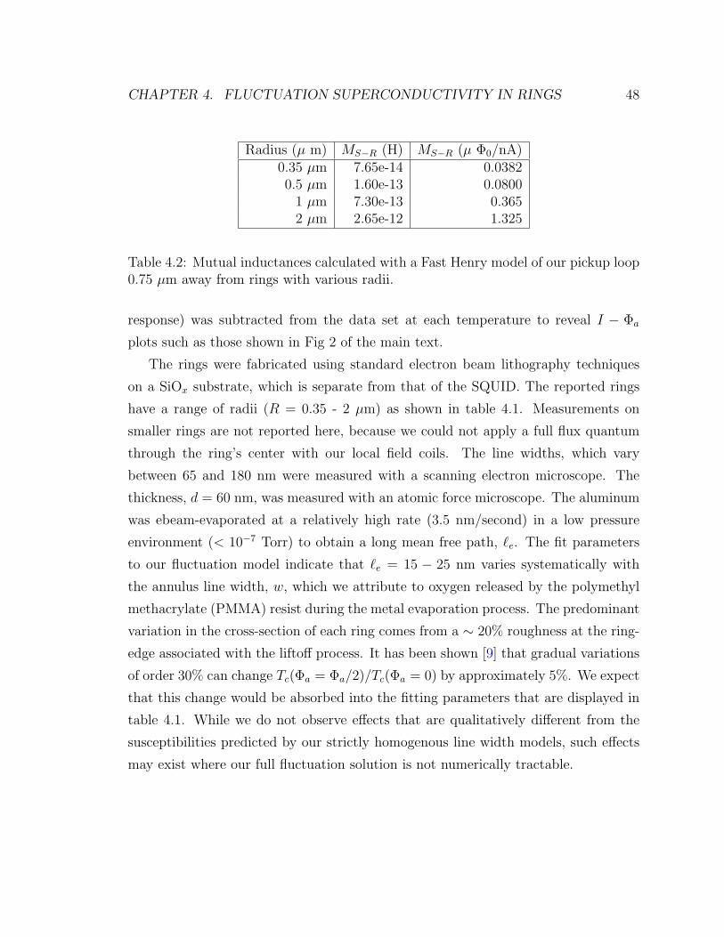
CHAPTER 4. FLUCTUATION SUPERCONDUCTIVITY IN RINGS 48
Radius (µ m) MS−R (H) MS−R (µ Φ0/nA)0.35 µm 7.65e-14 0.03820.5 µm 1.60e-13 0.0800
1 µm 7.30e-13 0.3652 µm 2.65e-12 1.325
Table 4.2: Mutual inductances calculated with a Fast Henry model of our pickup loop0.75 µm away from rings with various radii.
response) was subtracted from the data set at each temperature to reveal I − Φa
plots such as those shown in Fig 2 of the main text.
The rings were fabricated using standard electron beam lithography techniques
on a SiOx substrate, which is separate from that of the SQUID. The reported rings
have a range of radii (R = 0.35 - 2 µm) as shown in table 4.1. Measurements on
smaller rings are not reported here, because we could not apply a full flux quantum
through the ring’s center with our local field coils. The line widths, which vary
between 65 and 180 nm were measured with a scanning electron microscope. The
thickness, d = 60 nm, was measured with an atomic force microscope. The aluminum
was ebeam-evaporated at a relatively high rate (3.5 nm/second) in a low pressure
environment (< 10−7 Torr) to obtain a long mean free path, `e. The fit parameters
to our fluctuation model indicate that `e = 15 − 25 nm varies systematically with
the annulus line width, w, which we attribute to oxygen released by the polymethyl
methacrylate (PMMA) resist during the metal evaporation process. The predominant
variation in the cross-section of each ring comes from a ∼ 20% roughness at the ring-
edge associated with the liftoff process. It has been shown [9] that gradual variations
of order 30% can change Tc(Φa = Φa/2)/Tc(Φa = 0) by approximately 5%. We expect
that this change would be absorbed into the fitting parameters that are displayed in
table 4.1. While we do not observe effects that are qualitatively different from the
susceptibilities predicted by our strictly homogenous line width models, such effects
may exist where our full fluctuation solution is not numerically tractable.
CHAPTER 4. FLUCTUATION SUPERCONDUCTIVITY IN RINGS 49
4.2.2 Supplemental Online Text
The thermal fluctuations described in this study are theoretically grounded in the
Ginzburg-Landau free energy, F , for a 1D superconductor with periodic boundary
conditions. The rings are 1D in the sense that the wave function, ψ, is assumed
to only vary along x, the coordinate which is parallel to the circumference of the
ring. This assumption is valid when the annulus width, w, and thickness, d, are
much smaller than the temperature-dependent G-L coherence length, ξ(T ), which
determines the length scale for the energetic costs associated with changes in ψ. The
solution that minimizes the free energy of a homogeneous cross-section ring has the
form ψ(x) = |ψ| exp(i2πnx/L), where n is the phase-winding number guaranteed by
the single-valuedness of the wave function. The free energy [90, 91] for a solution of
this form is
F/V = α|ψ|2 +1
2β|ψ|4
+~
2m∗V
∫V
dV
(n
r+e∗
2~rB
)2
|ψ|2. (4.4)
where V is the volume of the ring and r is the radial coordinate. By minimizing
this free energy, one can obtain an expression for current, I, in a ring with finite
linewidth, as shown in [90]. This allows for a clean distinction between critical field
effects, associated with flux threading the annulus of the ring, and the pair-breaking
effects associated with the flux-induced Aharanov-Bohm phase around the ring’s cir-
cumference. To understand the Little-Parks effect [56], it is enough to consider the
w R limit (e.g. eq. 1 of the main text), where In is given by
In = − 1
λ2
wdΦ0
Lµ0
(Φa/Φ0 − n)P,
P = max
(1−
(2πξ(T )
L
)2
(Φa/Φ0 − n)2, 0
), (4.5)
This limit is appropriate because w, d λ(T ) which allows self screening effects
to be neglected. Critical field effects are negligible in our rings because the flux
CHAPTER 4. FLUCTUATION SUPERCONDUCTIVITY IN RINGS 50
captured in the annulus of the ring is much smaller than Φ0 for flux values discussed
here (Φa / Φ0/2). This last condition guarantees the strictly periodic response in
(Φa/Φ0−n), which is shown in the right inset to Fig. 2D. Above Tc(Φa) the agreement
with the 1D fluctuation theory (Fig. 2A-C) for a relatively wide (110 nm), small radius
(350 nm) ring demonstrates that the finite line-width effects are not essential to our
physical result.
At some temperature below Tc(Φa), our rings have a hysteretic response (similar
to fig 1 of [16]) that is associated with the multiple solutions to eq. 4.5 that are
possible when ξ(T ) < L/π . This metastability can be understood quantitatively
within the framework of thermally activated phase slips [53, 63] in the context of
superconducting rings [90, 16]. We believe that the data presented here is in thermal
equilibrium because it is sufficiently above the temperature where hysteresis occurs.
Our treatment is further justified by the fact that we focus on the temperatures where
ξ(T ) > L/π, where such metastable states are not theoretically possible.
Fluctuations are important when contributions from multiple wave function con-
figurations need to be considered to describe the ring’s response. A simple model [16]
estimates the equilibrium response with the Boltzmann distribution of fluxoid states.
This gives the expression
〈I(Φa)〉F =
∑n In exp(−En(Φa)/kBT )∑n exp(−En(Φa)/kBT )
(4.6)
where En(Φa) = −∫ Φa
nIndΦa is the energy associated with each local minimum of
the G-L free energy functional. While this model is not strictly applicable to our
data, because it cannot predict a response above Tc(Φa), it helps to illustrate some
of the important physics at half integer flux values. When Φa = (n + 12)Φ0, In and
In+1 contribute equally to the equilibrium current with contributions of equal and
opposite magnitude. The response thus goes through zero at the half-integer flux
values even when a mean field solution exists at that flux bias point. In this case, the
susceptibility can have a large magnitude due to the exponentially changing weight
of the fully condensed mean field states. When the superconducting response is small
(e.g. for our large γ rings when ξ(T ) / 2R), En ≈ kBT for several n states and a
CHAPTER 4. FLUCTUATION SUPERCONDUCTIVITY IN RINGS 51
large number of fluxoid states need to be considered, giving the significantly rounded
response well before Tc(Φa = Φ0/2). This phase-only model thus correctly describes
aspects of the ring behavior below Tc(Φa).
Both Gaussian and non-Gaussian fluctuations can allow for contributions from
wave function solutions that have local variations in their phase and amplitude. These
contributions are not included in the model described above, because all variation
around the ring is described by the single homogeneous phase winding determined
by n. The Gaussian response above Tc(Φa) can be derived by giving kBT of energy
to each fluxoid mode of a solution of the form ψ =∑
n cn exp(in2πx/L) [25]. This
process gives the expression
〈I〉G = 2kBTcΦ0
∞∑n=0
(Φa/Φ0 − n)
Θ/4 + (Φa/Φ0 − n)2(4.7)
where Θ ≡ 8π
(T−Tc)Ec/kB
is the temperature scale associated with the energetic cost of
a gradient in the wave function because Θ ≡ ±4R2/ξ(T )2. Gaussian fluctuations
can also be important below Tc(Φa) but in this case the solution must also take into
account the wave function response associated with the mean field response. The
model described by equation 4.7 predicts a γ-independent current that agrees well
with each ring at some γ dependent temperature above Tc(Φa).
To qualitatively understand the difference between Gaussian and non-Gaussian
fluctuations, one may consider a simplified free energy F (ψ) = α(Φa)|ψ|2 + 12β|ψ|4, in
which spatial variations of the order parameter are assumed to be frozen out, so that
its amplitude is the only variable. In this case one can define α(Φa) ∝ T − Tc(Φa)
to incorporate the flux dependence of Tc. A non-zero solution minimizes this expres-
sion below Tc(Φa), where α(Φa) is negative (β is defined to be positive). The term
“fluctuation response” refers to the response that cannot be described by this free
energy minimum alone, but requires the consideration of thermally activated fluctu-
ations around it. If these fluctuations can be calculated accurately by a quadratic
expansion of the free energy around its minimum, they are called “Gaussian”. This
occurs far above Tc(Φa), where ψ is small so that the α(Φa)|ψ|2 term dominates β|ψ|4.
Fluctuations are also Gaussian far below Tc(Φa), where the quadratic expansion can
CHAPTER 4. FLUCTUATION SUPERCONDUCTIVITY IN RINGS 52
be taken about the minimum of the so called “mexican hat” potential described by
a negative α(Φa) and positive β. As T approaches Tc(Φa), the vanishing of α(Φa)
leads to a divergence of 〈|ψ|2〉 as obtained from the quadratic expansion, which is
also reflected in eq. 4.7. It is in this regime, near Tc(Φa), that fluctuations become
“non-Gaussian” because the fluctuation amplitude is set by the β|ψ|4 term rather
than only the quadratic term. Thus, they can be thought of as interpolating between
the mean field response below Tc(Φa) and the Gaussian fluctuations that dominate at
high temperatures. The Ginzburg criterion determines the temperature range around
Tc(Φa) where non-Gaussian effects need to be considered by identifying where β〈ψ2〉2is comparable to or larger than α〈ψ2〉, (where 〈ψ2〉 is the overestimate derived from
Gaussian predictions). In our theory, β enters through γ ∝ βkBTcL3/wd, which shows
that it parametrizes the non-Gaussian term and thus controls non-Gaussian effects.
To apply the complete theory [83], we evaluate the contribution of all possible
wave functions, ψ, weighted according to their G-L energy, E[ψ], to the mean current
I ≡ −∂F/∂Φa = kBT∂∂Φa
lnZsc. The superconducting partition function, Zsc, is the
path integral over all possible wave functions: Zsc(Φa) =∫DψDψ∗ exp(−E[ψ]/kBT ).
Using the transfer operator technique [73], the evaluation of Zsc for a 1D ring [83] can
be transformed into a quantum mechanical eigenvalue problem. The flux-dependent
terms can be separated, so that one obtains
Zsc =∞∑
l=−∞
exp(−i2πlΦa/Φ0)∞∑n=0
exp(−γ1/3En,l) (4.8)
where En,l are the eigenvalues of the 2D single-particle Hamiltonian,
H = −1
2∇2 +
π2
2
Θ
γ2/3~r2 +
1
4~r4. (4.9)
We have rewritten these equations from the expression in reference [83] to emphasize
γ ≈ 16 kBTc
MeffEcand the dependence on the temperature scale Θ as defined above and
in the main text.
The fact that the Little-Parks line shape is washed out by fluctuations in large
γ rings can be understood qualitatively from the two components of γ. First, if
CHAPTER 4. FLUCTUATION SUPERCONDUCTIVITY IN RINGS 53
Tc/Ec is large, the entire Little-Parks temperature range is close to Tc(Φa = 0) and
it becomes difficult to differentiate the fluctuation effects at Φa = 0 and Φa/2. The
proportionality of γ to the cross section, entering through the number of channels,
M = k2Fwd/2π, reflects that it is energetically more costly to thermally excite a
certain order parameter amplitude over a larger volume.
While the theoretical analysis applies everywhere that a 1D G-L description is
correct in principle, numeric solutions become exponentially difficult for small γ rings
away from Tc(Φa = 0) Intuition for this difficulty can be derived from semiclassical
approximations to the lowest eigenvalue energies of Eq. 4.9. Above Tc, the Hamil-
tonian is positive definite with a lowest eigenvalue E0,0 ≈ 0 ⇒ Zsc ≈ 1. Because
the total partition function is the product of different states (Ztot = ZscZn...), Zsc
must be approximately constant above Tc(Φa). When the Little-Parks effect is sig-
nificant, this means that Zsc(Φa = Φ0/2) must also be approximately equal to one,
which leads to a difficulty in our formalism because the same eigenvalues must also
generate very large numbers at Φa = 0. For instance, when ξ = R below T (Φa = 0)
the lowest eigenvalue E0,0 can be estimated by the depth of the potential well in Eq
4.9 as E0,0 ≈ 4π4
γ4/3 . The value of the first term of the sum is thus ≈ exp 4∗π4
γ, which
can be 90 orders of magnitude larger than the value of Zsc at Φa = Φ0/2 for some of
our data points. We solved this problem through direct computation, but the expo-
nentially increasing difficulty means that further analysis of small γ rings will require
further insight or a new approach. Daumens et al. [25] have shown that the full non-
Gaussian response of two modes can be treated analytically, which should provide a
good approximation for small γ rings. Numeric techniques such as Monte Carlo or
TDGL-based Langevin simulations [8] could also provide further insight, particularly
in the case of non-homogeneous rings.
Chapter 5
Fluxoid Fluctuations in Mesoscopic
Superconducting Rings
Nicholas C. Koshnick, Hendrik Bluhm, Julie A. Bert , Kathryn A. Moler
A paper draft intended for submission to Physical Review Letters or Physical Review B
Abstract
Rings are a model system for understanding phase coherence in one dimension. Uni-
form superconducting rings exhibit metastable states whose phase winds uniformly
by an integer multiple of 2π around the ring. When the energy difference between
these states is less than or equal to the temperature, several states contribute to the
ring’s response in thermal equilibrium. We present magnetic susceptibility data and
a theoretical framework that demonstrate how these fluxoid fluctuations suppress the
ring’s diamagnetism below Tc. We also identify the parameters which determine the
crossover between the reduction of the response due to phase fluctuations and the
enhancement due to amplitude fluctuations.
54
CHAPTER 5. FLUXOID FLUCTUATIONS 55
5.1 Introduction
Fluctuations play an important role in the superconducting behavior of reduced di-
mensional samples: they can make electron pairing and long-range phase coherence
occur at different temperatures in unconventional superconductors[26], lead to the
Berezinskii-Kosterlitz-Thouless transition [51] in two dimensions (2D), cause the de-
struction of long range phase order in infinitely long one-dimensional (1D) wires [69],
and determine the resistive properties of 1D wires of finite length [53, 63, 29, 55].
We study the properties of 1D wires in a model system, uniform isolated alu-
minum rings. We focus on the case where the circumference is much longer than the
superconducting coherence length, ξ(T ). In this case one finds several metastable
states, which only differ by a phase winding, or fluxoid, number. Comparing the
response predicted from these phase-only solutions to experimental data and more
comprehensive theories allows for a clear distinction between phase and amplitude
fluctuations.
Transport measurements probing 1D fluctuations rely on the voltage generated
by changes in the phase winding value. We measure the current, I, as a function
of applied flux, Φa, which gives us access to the free energy, F . By measuring at
sufficiently high temperatures that phase slips occur rapidly compared to the mea-
surement time, we are able to probe the thermal effects associated with the energy
from phase winding about the entire ring, rather than the condensation energy of a
ring-section of length ξ, ie. the phase slip energy.
In this paper we show that the thermal distribution of fluxoid states suppresses the
ring’s diamagnetism below the mean field value. These results complement previous
studies of fluctuation effects in rings [90, 49], which mostly discuss the enhanced
diamagnetism caused by amplitude fluctuations at and above the superconducting
critical temperature, Tc. After presenting relevant ring data, we outline the theoretical
definition of the effect and state a criterion for where a downturn in the susceptibility
will occur. We then compare the fluxoid fluctuation effect to a theory that includes
all thermally induced fluctuations in the G.L. framework [73, 83]. We describe the
range of ring parameters where the simplified model is theoretically justified, and
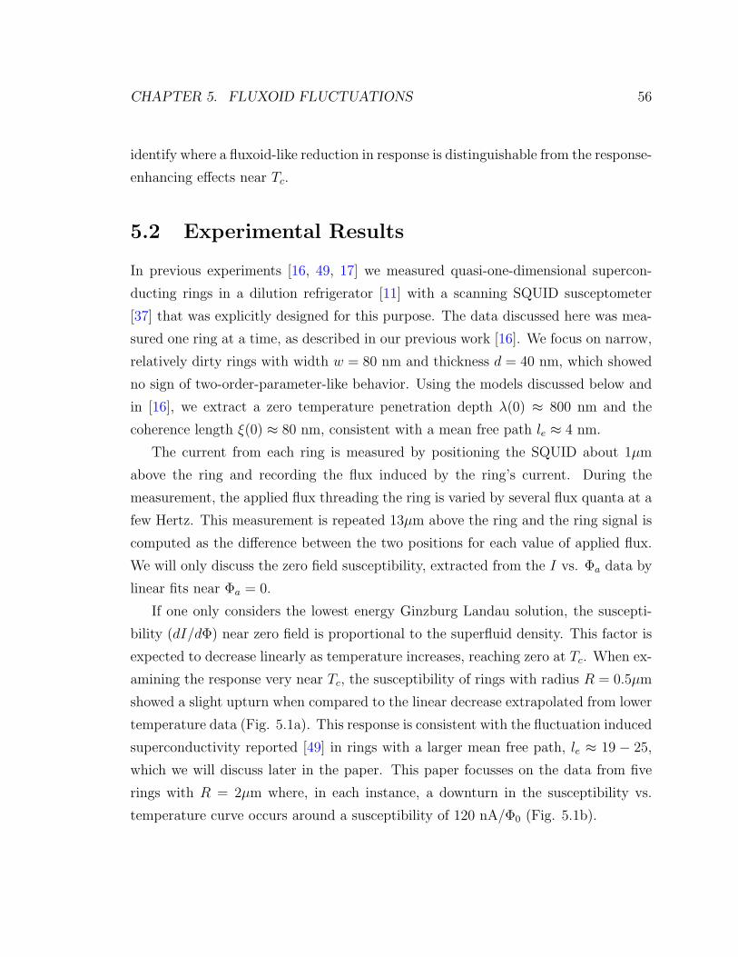
CHAPTER 5. FLUXOID FLUCTUATIONS 56
identify where a fluxoid-like reduction in response is distinguishable from the response-
enhancing effects near Tc.
5.2 Experimental Results
In previous experiments [16, 49, 17] we measured quasi-one-dimensional supercon-
ducting rings in a dilution refrigerator [11] with a scanning SQUID susceptometer
[37] that was explicitly designed for this purpose. The data discussed here was mea-
sured one ring at a time, as described in our previous work [16]. We focus on narrow,
relatively dirty rings with width w = 80 nm and thickness d = 40 nm, which showed
no sign of two-order-parameter-like behavior. Using the models discussed below and
in [16], we extract a zero temperature penetration depth λ(0) ≈ 800 nm and the
coherence length ξ(0) ≈ 80 nm, consistent with a mean free path le ≈ 4 nm.
The current from each ring is measured by positioning the SQUID about 1µm
above the ring and recording the flux induced by the ring’s current. During the
measurement, the applied flux threading the ring is varied by several flux quanta at a
few Hertz. This measurement is repeated 13µm above the ring and the ring signal is
computed as the difference between the two positions for each value of applied flux.
We will only discuss the zero field susceptibility, extracted from the I vs. Φa data by
linear fits near Φa = 0.
If one only considers the lowest energy Ginzburg Landau solution, the suscepti-
bility (dI/dΦ) near zero field is proportional to the superfluid density. This factor is
expected to decrease linearly as temperature increases, reaching zero at Tc. When ex-
amining the response very near Tc, the susceptibility of rings with radius R = 0.5µm
showed a slight upturn when compared to the linear decrease extrapolated from lower
temperature data (Fig. 5.1a). This response is consistent with the fluctuation induced
superconductivity reported [49] in rings with a larger mean free path, le ≈ 19 − 25,
which we will discuss later in the paper. This paper focusses on the data from five
rings with R = 2µm where, in each instance, a downturn in the susceptibility vs.
temperature curve occurs around a susceptibility of 120 nA/Φ0 (Fig. 5.1b).
CHAPTER 5. FLUXOID FLUCTUATIONS 57
1.49 1.5 1.51 1.52 1.53 1.540
50
100
150
200
Temp (K)
dI/d
Φ (
nA/Φ
0)
1.52 1.53 1.54 1.55
200
400
600
Temp (K)
dI/d
Φ (
nA/Φ
0)(a)
(b)
R = 0.5 µm
Tc = 1.552 K
R = 2 µm
Tc = 1.538 K
Figure 5.1: (Color Online) Zero field susceptibility (blue dots) as a function oftemperature for two rings with w = 80 nm, d = 40 nm. The black dotted linerepresents the expected susceptibility given by I ′0 (Eq. 5.3). a) Data from a ringwith R = 0.5 µm. The red line is a fit to Eqs. 5.7, 5.8, which can describe thefluctuation induced superconductivity above Tc. b) Data from a ring with R = 2 µm.The red line is the fluxoid fluctuation model (Eq. 5.5), which predicts a downturnwhen dI/dφ / 12kBT/Φ0 = 120 nA/Φ0 for T = 1.51K.
CHAPTER 5. FLUXOID FLUCTUATIONS 58
5.3 The Fluxoid Fluctuation Transition
Solutions that minimize the Ginzburg Landau free energy functional for a one dimen-
sional ring with n phase windings have free energies
FGL = −V B2c
µ0
(1− ξ(T )2
R2(φ− n)2
)2
. (5.1)
where Bc is the critical field, V is the ring volume, and µ0, the permeability of free
space, all enter into the ring’s total condensation energy. The dependence on ξ/R
accounts for the energy cost of n phase windings around the ring. The Aharonov-
Bohm phase gradient, φ = Φa/Φ0, associated with the applied flux in units of the
superconducting flux quantum, Φ0 = h/2e, can be transformed into a shift in the
boundary conditions for a wave function in a ring [19], and therefore contributes to
the energy in the same way as n.
Expanding this energy to the lowest order in ξ/R we get
En(φ) =I ′0Φ0
2(φ− n)2 − V B
2c
µ0
. (5.2)
where
I ′0 ≡ VB2c
µ0
4
Φ0
ξ2
R2= −wdΦ0
Lµ0
1
λ2. (5.3)
is the magnitude of the Meissner response I = − 1Φ0
∂F∂φ
= I ′0(φ− n) given in terms of
physical constants, geometric parameters, and the inverse squared penetration depth,
1/λ2, which is proportional to the super-fluid density.
Multiple phase winding states effect the ring response significantly when the en-
ergy difference between the lowest energy levels, ∆(En) = En=±1−En=0, is compara-
ble to kBT . This criteria is directly related to the Meissner currents that screen the
magnetic field.
If phase slips occur at a high enough rate, and the metastable fluxoid states are
in thermal equilibrium (see section 5.5), the resulting response can be modeled [16]
CHAPTER 5. FLUXOID FLUCTUATIONS 59
as a Boltzmann distribution of fluxoid states
I(φ)F =
∑n In exp(−En(φ)/kBT )∑n exp(−En(φ)/kBT )
. (5.4)
The derivative about φ = 0 is
dI
dφ
∣∣∣∣φ=0
= I ′0
(1−
∑n 2βn2 exp(−βn2)∑
n exp(−βn2)
)(5.5)
where β ≡ I ′0Φ0/2kBT . When β is large, terms with n 6= 0 are small and the
susceptibility is simply I ′0. When β < 6, the n = ±1 terms begin to play a significant
role, and the Meissner response is reduced by more than 5%. This allows us to define
dI
dφ≈ I ′0 <
12kBT
Φ0
. (5.6)
as a criterion for the visible onset of fluxoid fluctuations. A distinct down turn is
visible in Fig. 5.1 at this value (dI/dφ ≈ 0.1µA/φ0), around T = 1.51K. This down-
turn occurs close to Tc where the superfluid density decreases linearly with increasing
temperature. However, we note that fluxoid fluctuations are energetically allowed for
sufficiently long, thin rings, even for much larger superfluid densities at T Tc.
5.4 Relating Fluxoid and Non-Fluxoid Fluctuations
Thus far, we have considered a simplified description that explains the existence of
the downturn in susceptibility shown in figure 5.1b. In some of the data, near T = Tc,
the L ξ assumption is not strictly valid. In this case, the energy between successive
metastable states is no longer directly related to the Meissner current as described
above. Equation 5.4 is also not well behaved because incorporating the quartic term
of Eq. 5.1 requires the consideration of infinitely many states. Furthermore, our
treatment thus far has ignored phase oscillations that are not uniform around the ring
and amplitude oscillations of every kind. To address these issues, we compare our
simple fluxoid model to the model of von Oppen and Riedel, VOR [83], which allows
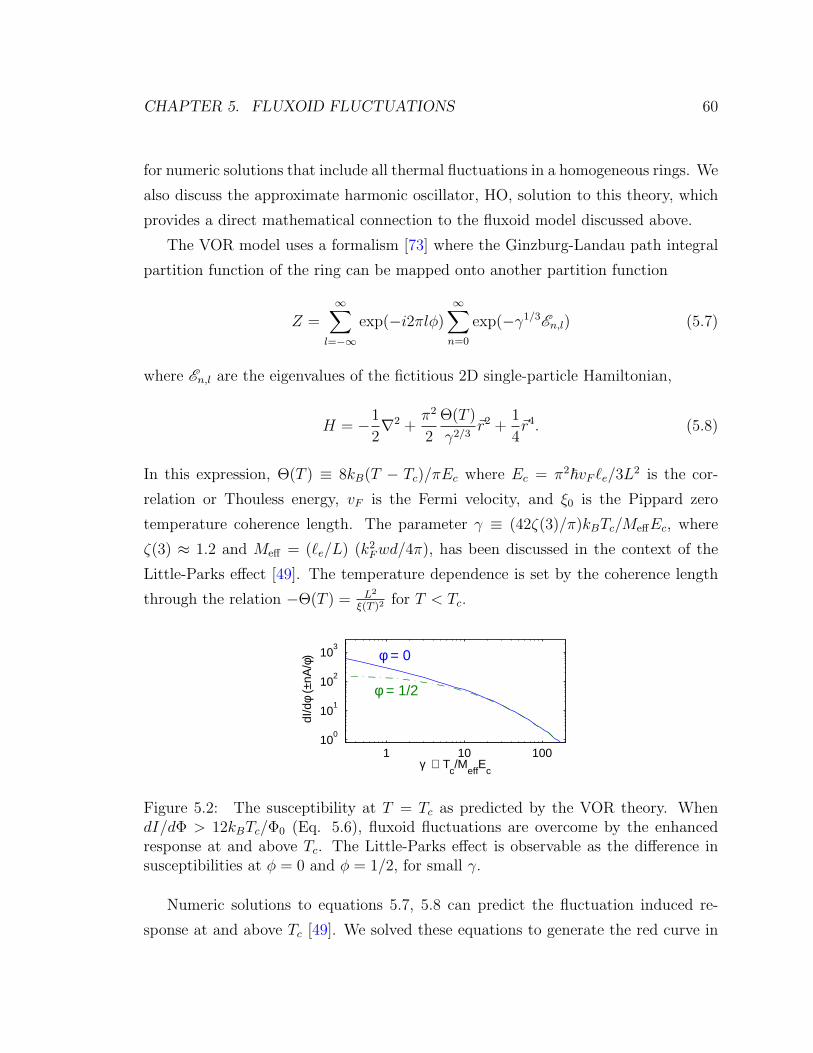
CHAPTER 5. FLUXOID FLUCTUATIONS 60
for numeric solutions that include all thermal fluctuations in a homogeneous rings. We
also discuss the approximate harmonic oscillator, HO, solution to this theory, which
provides a direct mathematical connection to the fluxoid model discussed above.
The VOR model uses a formalism [73] where the Ginzburg-Landau path integral
partition function of the ring can be mapped onto another partition function
Z =∞∑
l=−∞
exp(−i2πlφ)∞∑n=0
exp(−γ1/3En,l) (5.7)
where En,l are the eigenvalues of the fictitious 2D single-particle Hamiltonian,
H = −1
2∇2 +
π2
2
Θ(T )
γ2/3~r2 +
1
4~r4. (5.8)
In this expression, Θ(T ) ≡ 8kB(T − Tc)/πEc where Ec = π2~vF `e/3L2 is the cor-
relation or Thouless energy, vF is the Fermi velocity, and ξ0 is the Pippard zero
temperature coherence length. The parameter γ ≡ (42ζ(3)/π)kBTc/MeffEc, where
ζ(3) ≈ 1.2 and Meff = (`e/L) (k2Fwd/4π), has been discussed in the context of the
Little-Parks effect [49]. The temperature dependence is set by the coherence length
through the relation −Θ(T ) = L2
ξ(T )2 for T < Tc.
1 10 10010
0
101
102
103
γ ∝ Tc/M
effE
c
dI/d
φ (±
nA/φ
) φ = 0
φ = 1/2
Figure 5.2: The susceptibility at T = Tc as predicted by the VOR theory. WhendI/dΦ > 12kBTc/Φ0 (Eq. 5.6), fluxoid fluctuations are overcome by the enhancedresponse at and above Tc. The Little-Parks effect is observable as the difference insusceptibilities at φ = 0 and φ = 1/2, for small γ.
Numeric solutions to equations 5.7, 5.8 can predict the fluctuation induced re-
sponse at and above Tc [49]. We solved these equations to generate the red curve in
CHAPTER 5. FLUXOID FLUCTUATIONS 61
Fig. 5.1a. In Fig. 5.2, we show the susceptibility as a function of γ at T = Tc. At this
temperature, γ is the only sample dependent parameter . When the susceptibility
at T = Tc is greater than that given by Eq. 5.6, (eg. ≈120 nA for Tc = 1.5 K)
the fluctuation induced superconductivity at and above Tc masks the fluxoid effects
that can reduce the response below Tc. This indicates that a visible downturn in the
susceptibility cannot occur if γ . 10 when Tc ≈ 1.5K.
The presence of a visible upturn or downturn is demonstrated in the plots of the-
oretical susceptibilities as a function of temperature shown in Fig. 5.3. In this figure
we use the relation I ′0 = kBTc4π4Θ(T )/γΦ0 to compare the full theoretical response
to the simplified models. When γ = 3, the susceptibility at T = Tc is 140 nA, so a
downturn is not observable. When γ = 3100, the fluctuation induced superconduc-
tivity near T ≈ Tc is negligible, and the fluxoid induced downturn becomes visible
below Tc.
At some temperature sufficiently below Tc, the mexican hat potential given by
Eq. 5.8 is mostly parabolic near its minimum. In this case, non-Gaussian effects
should not play a significant role, and the eigenvalue solutions can be estimated by
a harmonic oscillator (HO) approximation. Solutions have the form ~r = |r| exp(ilφ),
so Eq. 5.8 can be written as a 1D problem, H = −12d2
dr2 + V (r) where
V (r) =l2
2r2+π2Θ(T )
2γ2/3r2 +
1
4r4. (5.9)
Expanding V (r) about its minimum at Rm(l) the eigenvalues have the form
En,l =l2
2Rm(l)2+Rm(l)4
4+ ω(n+ 1/2) (5.10)
where ω =√π2Θ(T )/2γ2/3 + 3Rm(l)2 + 3l2/Rm(l)4
Only terms that change with l, the angular momentum coordinate in the fictitious
Hamiltonian, contribute to the flux dependence of the partition function, thus only
these terms can contribute to the thermodynamic ring-current. If we only include the
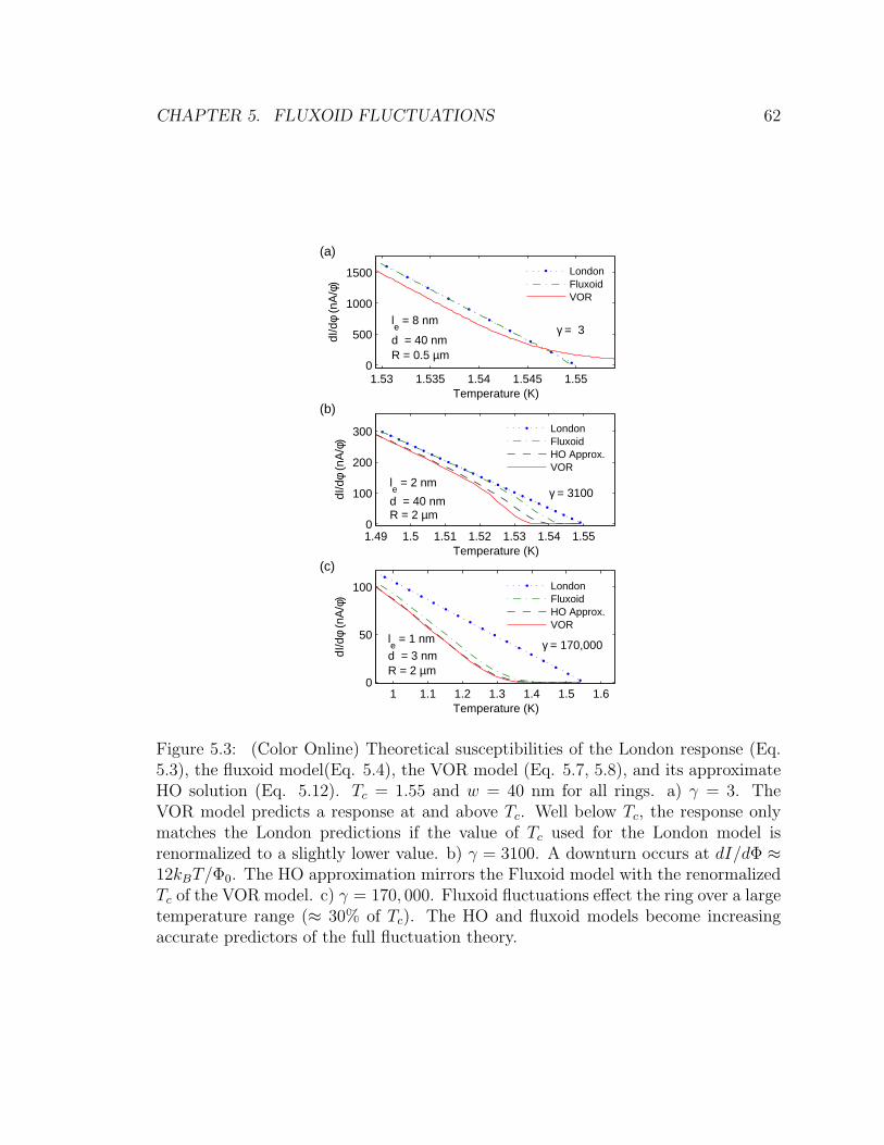
CHAPTER 5. FLUXOID FLUCTUATIONS 62
1.53 1.535 1.54 1.545 1.550
500
1000
1500
Temperature (K)
dI/d
φ (n
A/φ
)
R = 0.5 µmd = 40 nm
le = 8 nm
γ = 3
LondonFluxoidVOR
1.49 1.5 1.51 1.52 1.53 1.54 1.550
100
200
300
Temperature (K)
dI/d
φ (n
A/φ
)
R = 2 µmd = 40 nm
le = 2 nm
γ = 3100
LondonFluxoidHO Approx.VOR
1 1.1 1.2 1.3 1.4 1.5 1.60
50
100
Temperature (K)
dI/d
φ (n
A/φ
)
R = 2 µmd = 3 nm
le = 1 nm γ = 170,000
LondonFluxoidHO Approx.VOR
(a)
(b)
(c)
Figure 5.3: (Color Online) Theoretical susceptibilities of the London response (Eq.5.3), the fluxoid model(Eq. 5.4), the VOR model (Eq. 5.7, 5.8), and its approximateHO solution (Eq. 5.12). Tc = 1.55 and w = 40 nm for all rings. a) γ = 3. TheVOR model predicts a response at and above Tc. Well below Tc, the response onlymatches the London predictions if the value of Tc used for the London model isrenormalized to a slightly lower value. b) γ = 3100. A downturn occurs at dI/dΦ ≈12kBT/Φ0. The HO approximation mirrors the Fluxoid model with the renormalizedTc of the VOR model. c) γ = 170, 000. Fluxoid fluctuations effect the ring over a largetemperature range (≈ 30% of Tc). The HO and fluxoid models become increasingaccurate predictors of the full fluctuation theory.
CHAPTER 5. FLUXOID FLUCTUATIONS 63
l2/2Rm(0)2 term, the current is
I = kBT1
Z
∂
∂Φa
Zsc =
∑n 2πl sin (2πlφ) exp(l2γ/π2Θ(T ))∑n cos (2πlφ) exp(l2γ/π2Θ(T ))
(5.11)
which is exactly equivalent to equation 5.4. Including the second two terms of Eq.
5.10, which account for the angular momentum dependence of ω and Rm(l), we get
Z =∞∑
l=−∞
exp(−i2πlφ) exp(−γ1/3V (Rm(l)))
× exp(−γ1/3ω/2)
1− exp(−γ1/3ω)(5.12)
Figure 5.3b,c show the results from the simple fluxoid model (Eqs. 5.4, 5.11, dashed
green lines), and this HO approximation (dashed black lines) alongside the VOR
model (Eq. 5.7, 5.8, solid red) and the London response (Eq.5.3, dotted blue). The
HO solution qualitatively reproduces the downturn in susceptibility of the fluxoid
model. One striking difference is that both the VOR model and its HO approximation
have an offset in the linear regime far below Tc when compared to the London or
fluxoid model. This can be described as an apparent renormalization in Tc due to the
consideration of all possible fluctuation modes.
When γ is in the range of a few thousand (Fig. 5.3c), the VOR model predicts
more of a downturn in the susceptibility than is predicted by the fluxoid or HO mod-
els, which is presumably due to contributions from non-homogeneous phase winding
solutions, amplitude fluctuations, or both. When γ is substantially larger, the fluxoid
fluctuation effect occurs far below Tc. In this case, the harmonic oscillator and Tc
shifted fluxoid models are in good agreement with the more complete theory, indicat-
ing that that fluxoid fluctuation approximation is valid.
Superconducting phase slips in one dimensional wires have been the subject of
theoretical and experimental interest for several decades. While phase slips deter-
mine the onset of resistance, the fluxoid process we describe here causes the loss of
another hallmark of superconductivity, the ability to screen magnetic field. Our rings
are a model 1D system that is easy to manipulate with modern fabrication techniques.
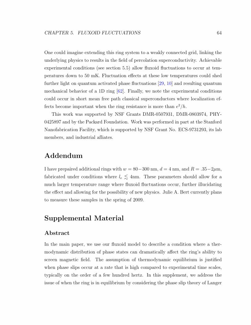
CHAPTER 5. FLUXOID FLUCTUATIONS 64
One could imagine extending this ring system to a weakly connected grid, linking the
underlying physics to results in the field of percolation superconductivity. Achievable
experimental conditions (see section 5.5) allow fluxoid fluctuations to occur at tem-
peratures down to 50 mK. Fluctuation effects at these low temperatures could shed
further light on quantum activated phase fluctuations [29, 10] and resulting quantum
mechanical behavior of a 1D ring [62]. Finally, we note the experimental conditions
could occur in short mean free path classical superconductors where localization ef-
fects become important when the ring resistance is more than e2/h.
This work was supported by NSF Grants DMR-0507931, DMR-0803974, PHY-
0425897 and by the Packard Foundation. Work was performed in part at the Stanford
Nanofabrication Facility, which is supported by NSF Grant No. ECS-9731293, its lab
members, and industrial afliates.
Addendum
I have prepaired additional rings with w = 80−300 nm, d = 4 nm, and R = .35−2µm,
fabricated under conditions where le . 4nm. These parameters should allow for a
much larger temperature range where fluxoid fluctuations occur, further illucidating
the effect and allowing for the possibility of new physics. Julie A. Bert currently plans
to measure these samples in the spring of 2009.
Supplemental Material
Abstract
In the main paper, we use our fluxoid model to describe a condition where a ther-
modynamic distribution of phase states can dramatically affect the ring’s ability to
screen magnetic field. The assumption of thermodynamic equilibrium is justified
when phase slips occur at a rate that is high compared to experimental time scales,
typically on the order of a few hundred hertz. In this supplement, we address the
issue of when the ring is in equilibrium by considering the phase slip theory of Langer
CHAPTER 5. FLUXOID FLUCTUATIONS 65
and Ambegaokar [53] as formulated for rings [91, 90].
5.5 Conditions for Equilibrium
The phase slip theory of Langer and Ambegaokar [53] as formulated for rings [91, 90],
predicts a phase slip rate, by calculating the lowest energy pathway between two
fluxoid states as defined by the energy barrier for the saddle point in wave function
configuration space. The saddle point energy is
Fsaddle = Fc
(4√
2δ
3
ξ
L− (2 + δ)2
18
)(5.13)
where Fc ≡ wdLB2c/µ0 is the ring’s condensation energy and δ is a real number
between 0 and 1 that satisfies the relation
2πn =2√3
L
ξ
√1− δ2
+ 2 tan−1
(√3δ
2(1− δ)
)+ 2πφ. (5.14)
In the regime of interest L ξ, δ must be close to one. By using the substitution
δ = 1 − (ε ξL
)2, expanding to lowest order in ξ/L, and solving for ε, we arrive at a
simplified expression
δ = 1−(√3π(2n− 2φ− 1)
Lξ− 2√
2
)2
. (5.15)
Going back to the energy expression, we can see that the lowest flux indepen-
dent terms give Fsaddle = Fc(4√
2ξ/3L − 1/2) (red dotted line in fig 5.4). As ξ/L
becomes increasingly small, the flux dependent nature of both Fsaddle and FGL be-
come less important to the energy difference ∆Esaddle = Fsaddle − FGL leaving only
this flux-independent term. While Fc is proportional to the volume of the entire ring,
∆Esaddle ≈ 3.8wdξB2c/µ0 is proportional to the condensation energy of a section of
the ring of length ξ. The criterion for phase slips is therefore physically distinct from
the energy difference, ∆EGL = En=±1 −En=0 as defined by Eq. 2 in the main paper,
that determines the temperature where fluxoid fluctuations occur. However, in the
limit where L ξ, the fluxoid condition is already satisfied when phase slips begin
CHAPTER 5. FLUXOID FLUCTUATIONS 66
−0.5 0 0.5 1 1.5−1
−0.9
−0.8
−0.7
Applied Flux (Φ0)
Fc
FGL
Fsaddle
n= −1 n= 0 n= 1
−1,0 0,1
−0.5 0 0.5 1 1.5
−1
−0.98
−0.96
−0.94
Applied Flux (Φ0)
Fc
FGL
Fsaddle
n= −1 n= 0 n= 1
−1,0 0,1
(a) (b)
Figure 5.4: Fluxoid (solid) and saddle point (dashed) energies as a function ofapplied flux, in units of the condensation energy. The red dotted line is ≈ 3.8 timesthe condensation energy for a ring section of length ξ. a The respective energies whenL/ξ(T ) = 80. b The respective energies when L/ξ(T ) = 30. The fluxoid fluctuationenergy ∆EGL = En=±1 − En=0 scales differently than ∆Esaddle.
to occur, so in the longest wires both the fluxoid fluctuation and thermally induced
phase slip effects have the same onset temperature.
Given the the saddle point energies, we can estimate the phase slip rate as:
R = Ω exp
(−(Fsaddle − FGL)
kBT
)(5.16)
The prefactor, Ω = (L/ξ)(Fsaddle − FGL/kBT )1/2/τ , was derived based on arguments
using the time dependent Ginzburg Landau model [63], where τ = πh/8kB(Tc−T ) is
the relaxation time. In this formulation, the temperature dependence of the exponent
is set by ξ(T ) and λ(T ). Aluminum with le = 4nm has λ(0) ≈ 800nm and ξ(0) ≈85nm. Using standard temperature dependences for these parameters, a ring of this
material with w = 80nm and d = 40nm will have switching occur on experimental
time scales down to 1.1 K when Tc ≈ 1.24, while a ring with d = 4nm will continue
to have phase slips down to 0.45 K. Already, in this range, the foundations of time-
dependent and time-independent Ginzburg Landau theory are invalid, and quantum
fluctuations may play an important role [29, 10]. In future fabrication runs, we can
extend the testable regime by further tweaking physical parameters. For instance,
using the same model with le = 1 nm, d = 2 nm, and w = 30 nm, phase slips are
predicted to occur at a high rate down to a temperature of 50 mK.
Chapter 6
Towards Superconducting Rings
Where Ec > kBTc
In this chapter, I describe my efforts to fabricate and measure small, clean rings where
the Thouless or correlation energy, Ec, is greater than or approximately equal to Tc.
When considering this problem, an important limit is the amount of field that we can
apply with the on-chip field coils. If we only consider rings where we can apply at
least half a flux quantum of field, we are limited to rings that have a radius R ' 350
nm. This sets a limit to the extent by which Ec ∝ vF le/R2 can be increased simply
by reducing R. After briefly discussing the exciting new physics in this regime, we will
discuss our efforts to make cleaner rings (e.g. longer le) and clean rings with reduced
Tc.
67
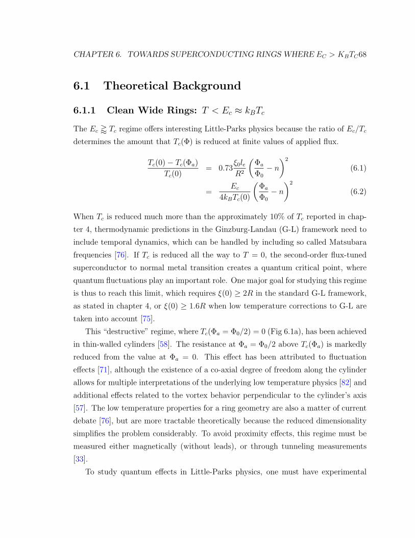
CHAPTER 6. TOWARDS SUPERCONDUCTING RINGS WHERE EC > KBTC68
6.1 Theoretical Background
6.1.1 Clean Wide Rings: T < Ec ≈ kBTc
The Ec ' Tc regime offers interesting Little-Parks physics because the ratio of Ec/Tc
determines the amount that Tc(Φ) is reduced at finite values of applied flux.
Tc(0)− Tc(Φa)
Tc(0)= 0.73
ξ0leR2
(Φa
Φ0
− n)2
(6.1)
=Ec
4kBTc(0)
(Φa
Φ0
− n)2
(6.2)
When Tc is reduced much more than the approximately 10% of Tc reported in chap-
ter 4, thermodynamic predictions in the Ginzburg-Landau (G-L) framework need to
include temporal dynamics, which can be handled by including so called Matsubara
frequencies [76]. If Tc is reduced all the way to T = 0, the second-order flux-tuned
superconductor to normal metal transition creates a quantum critical point, where
quantum fluctuations play an important role. One major goal for studying this regime
is thus to reach this limit, which requires ξ(0) ≥ 2R in the standard G-L framework,
as stated in chapter 4, or ξ(0) ≥ 1.6R when low temperature corrections to G-L are
taken into account [75].
This “destructive” regime, where Tc(Φa = Φ0/2) = 0 (Fig 6.1a), has been achieved
in thin-walled cylinders [58]. The resistance at Φa = Φ0/2 above Tc(Φa) is markedly
reduced from the value at Φa = 0. This effect has been attributed to fluctuation
effects [71], although the existence of a co-axial degree of freedom along the cylinder
allows for multiple interpretations of the underlying low temperature physics [82] and
additional effects related to the vortex behavior perpendicular to the cylinder’s axis
[57]. The low temperature properties for a ring geometry are also a matter of current
debate [76], but are more tractable theoretically because the reduced dimensionality
simplifies the problem considerably. To avoid proximity effects, this regime must be
measured either magnetically (without leads), or through tunneling measurements
[33].
To study quantum effects in Little-Parks physics, one must have experimental
CHAPTER 6. TOWARDS SUPERCONDUCTING RINGS WHERE EC > KBTC69
Figure 6.1: Diagram of Tc as a function of applied flux. The gray scale in the re-gion indicates the relative importance of fluctuation effects above Tc(Φa), with darkerregions having the potential for stronger fluctuation effects. a) Diagram of an Alu-minum ring with Tc(0) = 1.15. b) A bilayer ring with Tc(0) = .3.
access to temperatures well below Tc. In some sense, this represents a trade-off,
because materials with lower Tc’s have a longer zero-temperature coherence length
(ξ(0) ∝ 1/Tc), and thus are more affected by the Little-Parks effect. We have primar-
ily worked with aluminum (Al) because it is a well-known material with a relatively
low Tc and a relatively long mean free path. In Al, ξ0 ≈ 1.6 is much larger than le,
so ξ(0) ∝ √leξ0. Section 6.2 will primarily talk about mean free path engineering of
aluminum, in an attempt to reach the destructive regime.
In practice, the finite line-width, w, of superconducting rings can allow for addi-
tional reduction in Tc(Φa) in two ways. First, wider rings tend to have a larger le (see
table 4.1), presumably due to less edge scattering and less oxidation effects from the
outgassing of nearby PMMA during the metal deposition process. Second, wide rings
have a lower critical field, Hc2. Critical field effects reduce Tc with increasing flux,
which adds to the strictly 1D, periodic Little-Parks physics, shown in figure 6.1. This
means that finite-width rings can have Tc(Φ = Φ0/2) = 0 even when their coherence
length and radius would predict that they would not reach the destructive regime if
one only considers equation 6.2.
Zhang and Price [90, 91] derived an expression for the Ginzburg Landau free
energy for rings with finite width. After minimizing this expression, they found the
CHAPTER 6. TOWARDS SUPERCONDUCTING RINGS WHERE EC > KBTC70
current
I =
(n−
(1 +
w2
4R2
)Φa
Φ0
)min
[1− ξ(0)2
R2
((n− Φa
Φ0
)2
+w2
4R2∗(n2
3+
Φa
Φ0
2)), 0
].
(6.3)
This expression has terms that relate to both flux focusing and Hc2 effects in a some-
what non-trivial way. Analyzing the conditions when I = 0, Φa 6= 0, yields us a plot
of Tc(Φa), from which we can derive a Tc versus Φa that has a decreasing phase with
additional applied field. This effect is, of course, also important for superconducting
cylinders, where the combination of Little-Parks and Hc physics has already been
discussed [57]. The first w/2R term in equation 6.3 increases the effective applied
flux, allowing us to study smaller rings. The reduction in Tc due to the second term
with w/2R also allows rings to more easily reach Tc(Φa = Φ0/2) = 0. Clearly, this
effect is limited to the case where w = R, at which point the ring becomes a disc.
The Little-Parks effect can most easily be distinguished from Hc effects when super-
conductivity re-emerges at an applied flux value |Φa| ≈ Φ0/2. For rings with radii R
= 300 nm, this sets a limit on ξ(T ) > 500 nm.
6.1.2 Bilayers: T < Tc < Ec
A second approach to reach the limit where Ec > Tc is to maintain cleanliness while
reducing Tc by making the ring from a bilayered superconducting/normal metal ma-
terial. The physical intuition for the advantage of this approach does not rely on the
fact that in pure metals, ξ(0) ∝ ξ0 ∝ 1/Tc, which is probably not true for a proximity-
effect reduced Tc. Rather, the curvature of the ring’s Tc(Φa) phase diagram is set by
some coherence length that should not reduce much in the bilayered material. By
using the proximity effect to reduce Tc, there is a smaller temperature range to which
the Tc(Φa) must to be lowered, in order to reach Tc(Φ0/2) = 0 (Eq.6.2, Fig. 6.1). In-
tuition for this logic stems from the Usadel equations, where a single-order parameter
describes the superconducting response to Little-Parks-like phase gradients, Tc low-
ering magnetic impurities, or magnetic fields [4] Thus, in this simplified picture, the
Tc reducing proximity effect and Little-Parks effect can be summed independently.
CHAPTER 6. TOWARDS SUPERCONDUCTING RINGS WHERE EC > KBTC71
Although the Usadel theory formally only applies to homogeneous systems, similar
logic might apply even with the introduction of normal metal layers.
A bilayer ring in the Cooper limit can can be modeled as a superconductor with
a transverse-direction-independent order parameter and new physical parameters λ
and ξ. This limit requires that the thickness of both layers is d / le, and that the
transmission coefficient between layers is sufficiently large. If a highly conductive
noble metal is used for the normal metal layer, the ring can also have an increased le
which in turn increases Ec.
The successful implementation of a SC/N ring could always allow for Ec kBTc,
if Tc is made to be arbitrarily small. The question then becomes what values are
experimentally accessible. SQUID radiation on the sample limits effective ring tem-
peratures to ∼ 200 mK [15]; thus in our experimental setup, many bilayered systems
may only be measured in a regime where T > Ec/kB > Tc. Even so, this limit presents
an interesting regime that is intimately related to the h/2e persistent current physics
in normal metal rings or the response of aluminum rings above Hc2 [13]. In the Gaus-
sian region above Tc, the magnitude of fluctuation is ∝ Tc/Φ0. The magnitude of h/e
persistent currents is ∝ Ec/Φ0 [70]. Thus, by varying the superconductor or normal
metal layer thicknesses, one can reach a limit where the two effects co-exist.
Clean, low-Tc, 2D materials have received attention in the superconductor-metal
transition literature recently as a regime where even small amounts of disorder could
lead to large spacial variations in the superconducting properties [78]. This prediction
may manifest itself as enhanced mesoscopic fluctuations in measurements of a large
number of nominally identical rings. Such a result would considerably extend the
G-L description of the way inhomogeneities affect the Little-Parks effect [9].
The exact behavior of bilayered samples is difficult to relate to the physics dis-
cussed in chapter 4 because it is not clear whether the mesoscopic parameters that
characterize γ have the same role in a bilayered system as they do in pure classical
superconductors. That fact aside, it is interesting to note that a clean, low Tc super-
conductor, governed by standard G-L theory, would have different criteria for where
the Little-Parks line-shape may be washed out by fluctuations. This is because the
magnitude of susceptibility, shown for instance in figure 4.3c, needs to be scaled with
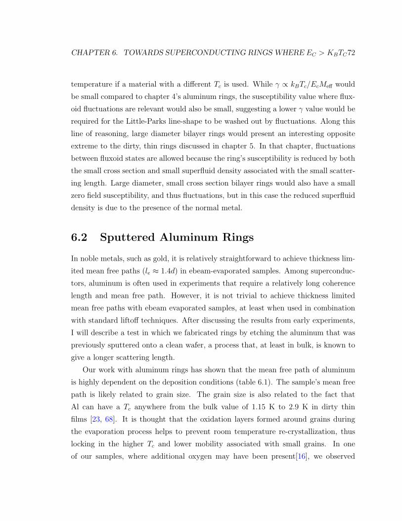
CHAPTER 6. TOWARDS SUPERCONDUCTING RINGS WHERE EC > KBTC72
temperature if a material with a different Tc is used. While γ ∝ kBTc/EcMeff would
be small compared to chapter 4’s aluminum rings, the susceptibility value where flux-
oid fluctuations are relevant would also be small, suggesting a lower γ value would be
required for the Little-Parks line-shape to be washed out by fluctuations. Along this
line of reasoning, large diameter bilayer rings would present an interesting opposite
extreme to the dirty, thin rings discussed in chapter 5. In that chapter, fluctuations
between fluxoid states are allowed because the ring’s susceptibility is reduced by both
the small cross section and small superfluid density associated with the small scatter-
ing length. Large diameter, small cross section bilayer rings would also have a small
zero field susceptibility, and thus fluctuations, but in this case the reduced superfluid
density is due to the presence of the normal metal.
6.2 Sputtered Aluminum Rings
In noble metals, such as gold, it is relatively straightforward to achieve thickness lim-
ited mean free paths (le ≈ 1.4d) in ebeam-evaporated samples. Among superconduc-
tors, aluminum is often used in experiments that require a relatively long coherence
length and mean free path. However, it is not trivial to achieve thickness limited
mean free paths with ebeam evaporated samples, at least when used in combination
with standard liftoff techniques. After discussing the results from early experiments,
I will describe a test in which we fabricated rings by etching the aluminum that was
previously sputtered onto a clean wafer, a process that, at least in bulk, is known to
give a longer scattering length.
Our work with aluminum rings has shown that the mean free path of aluminum
is highly dependent on the deposition conditions (table 6.1). The sample’s mean free
path is likely related to grain size. The grain size is also related to the fact that
Al can have a Tc anywhere from the bulk value of 1.15 K to 2.9 K in dirty thin
films [23, 68]. It is thought that the oxidation layers formed around grains during
the evaporation process helps to prevent room temperature re-crystallization, thus
locking in the higher Tc and lower mobility associated with small grains. In one
of our samples, where additional oxygen may have been present[16], we observed
CHAPTER 6. TOWARDS SUPERCONDUCTING RINGS WHERE EC > KBTC73
line-width-dependent Tc’s of up to 1.9 K. In general, longer le’s are achieved when
thicker/wider samples (less edge scattering) are evaporated at high deposition rate,
on a warm sample substrate (both associated with larger grains), in a chamber with
a lower vapor pressure (less oxygen and other impurities).
Table 6.1: Aluminum film properties during three sample fabrication processes. Themean free path, le, was determined from the effect ξ has on the ring’s response.
Reference Deposition Rate Pressure Film Thickness le[49] ∼ 30 A/sec 1× 10⁻⁷ torr 60 nm 14-25 nm[16] ∼ 1 A/sec ∼ 1× 10⁻⁶ torr 40 nm 4 nm[2] ∼ 0.1 A/sec 5.7× 10⁻⁷ torr 4 nm non-SC
Our experience with the variables listed above suggests that it will be difficult
to fabricate samples with ebeam evaporators that have mean free paths that are
substantially larger than the values presented in table 6.1. Without increasing le
substantially, ∆Tc(Φa)/Tc(0) will be reduced by no more than ∼6% of Tc(Φa = 0).
Noble-metal-like mean free paths may be possible in aluminum created by other
means such as MBE. Notably, it is thought that sputter evaporated aluminum films
can also have thickness limited mean free paths in some cases [61]. The combination
of line-width effects (∼ 30%) and the low temperature reduction in the coherence
length criterium (20%) means that a Tc(Φa = Φ0/2) = 0 could be achieved with
ξ(0) = 400 nm or le = 140 nm for a 350 nm radius ring. Since even rings with
∆Tc(Φa)/Tc(0) ≈ 50% present the possibility of exciting new physics, we fabricated
sputtered aluminum rings and present the results in this section.
We received a 200 nm thick aluminum on silicon sample grown by Erik Lucero
in the Martinis Group at University of California at Santa Barbara in a dedicated
aluminum sputtering system. We fabricated rings with a chlorine based reactive ion
etch process in the Plasma Quest R© at Stanford Nano-Fabrication facility (SNF). The
sparse rings were patterned with ebeam lithography using Ma-N 2403, a novolac-
based negative-tone resist. We found that doses that created the intended features
also created a resist scum halo, presumably due to electron backscattering, which
sometimes extended more than a micron over the nearby area (Fig. 6.2b). This
scum acted as an effective etch stop (Fig. 6.2c). The minimum dose-to-clear varied
CHAPTER 6. TOWARDS SUPERCONDUCTING RINGS WHERE EC > KBTC74
−50 −25 0 25 50H
applied (Oe)
Re
sist
an
ce (
arb
.)
500 nm2 µm
(a) (b) (c)
Figure 6.2: a) Resistance of a sputtered aluminum film as a function of appliedfield, demonstrating a critical field of 24.5 Gauss. b) Ma-N 2403 negative-tone resistpatterned by ebeam lithography. The large dark area is thought to be resist scum.Note the large grain size in the aluminum film. c) The resist scum acts as an effectiveetch stop when making rings. The scum was minimized by varying the dose, beamacceleration, and using various amounts of oxygen plasma etching as a precursor tothe ring etch process.
considerably with radius and line width, and the scum was not effectively removed
by an oxygen plasma de-scum recipe designed to cut through ≈ 30 nm of resist. A
suitable array of rings was created using a combination of these methods: an oxygen
de-scum recipe, which removed ≈ 115 nm of the ≈ 350 nm thick resist, and three
separate dose factors for each combination of ring parameters.
Low temperature measurements of the bulk film and the above-mentioned rings
revealed limits to the use of sputtered aluminum as an ultra-clean material. The
critical field (Hc2) of bulk films was 24.5 Gauss at 0.51 K, which corresponds to a
coherence length ξ(0.51) = 366 nm. Extrapolating this to zero temperature using
a standard G-L temperature dependence gives ξ(0) ≈ 300 nm, from which we can
derive le = 1.4ξ(0)2/ξ0 ≈ 80 nm. This le is not thickness-limited, but it is better than
what we have observed in ebeam evaporated films (Table 6.1).
The ring fabrication reduced the bulk film le, ξ(0) considerably. This may be due
to corrosion from the Cl etch, or from additional edge scattering from the large grain
structure that is apparent in Fig 6.2a,b. Fitting the cubic component of ring I − Φ
curves, we find ξ ≈ 90 nm at 0.25 K, which corresponds to ξ(0) ≈ 80 nm or le ≈ 5 nm.
CHAPTER 6. TOWARDS SUPERCONDUCTING RINGS WHERE EC > KBTC75
Another check on the cleanliness of the rings, which would lead to a larger but still
not large enough le, is that the Little-Parks effect was observable, but the minimum
Tc(Φa) was no more than 15% below Tc(0). Difficulties with dilution refrigerator
operation lead to the conclusion of this cool down without significant further results.
6.3 Normal Metal/Superconductor Bilayer Rings
The normal/superconductor bilayer idea was originally suggested to us by John
Price at the University of Colorado - Boulder. He was exposed to the concept
through interactions with the transition edge sensor (TES) community after Xiax-
ian Zhang’s unsuccessful attempts to create Ec > Tc superconducting rings with
normal/superconductor alloys. TES sensors and our rings require similar features,
but for separate reasons. X-ray/infrared analysis requires large pixel sizes and fast
thermal response times (e.g. clean films). A low, tunable Tc allows for optimal ther-
mal noise, typically achieved when Tc ≈ 100−200 mK. In this context, several groups
have tested a number of material combinations, including Cu/Mo [38, 34], Au/Mo
[20], Al/Ag [89], AlMn/Al [74].
Making bilayered materials with a high transmission coefficient can be challenging.
Known issues include oxididation, film stress, impurity levels, corrosion, and interdi-
fussion. Because of these issues, we based our work on a previously engineered system
of Cu/Mo, although our project complicates this further with the sub-micron ring
line widths. The primary difficulty with this particular combination is the all known
chemical etchants that remove copper remove Molybdenum much more aggressively,
resulting in interlayer undercutting and roughness that can extend microns from the
edge point of a desired feature. The current TES solution is to use normal metal
capping layers (Fig 6.3) that provide boundary conditions that reduce edge effects
[35]. Such a solution would be very difficult to implement effectively in sub-micron
rings.
We worked with a 140 mK Tc, 70 nm thick Cu, 45 nm thick Molybdenum sample,
given to us by Gene Hilton at N.I.S.T.-Boulder. Our sparse small-featured rings
required ebeam lithography on a negative-tone resist. As described in the previous
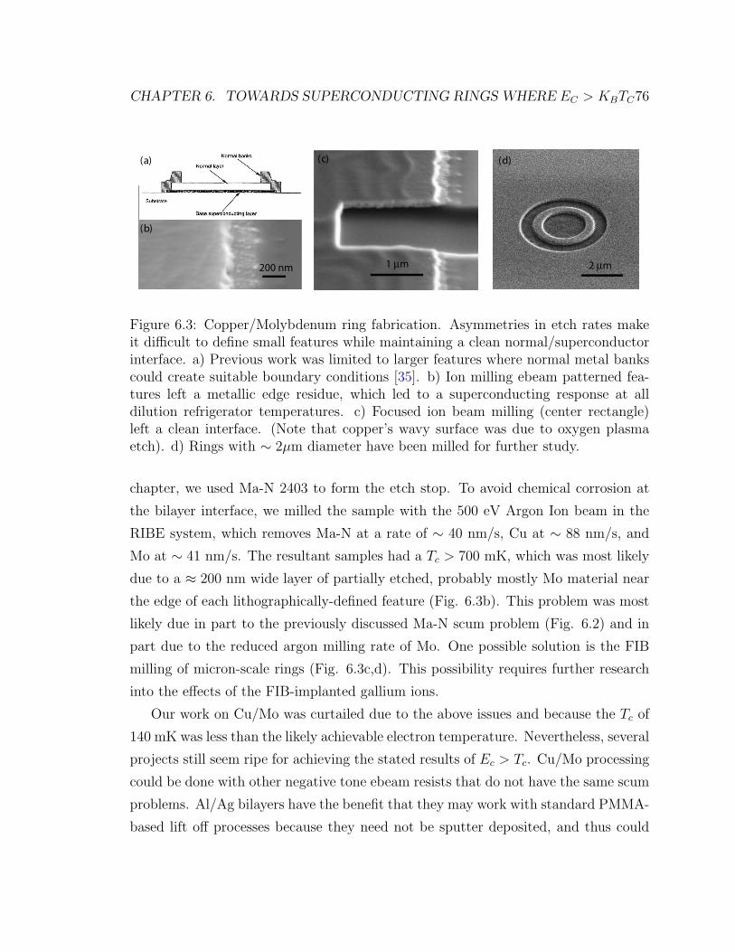
CHAPTER 6. TOWARDS SUPERCONDUCTING RINGS WHERE EC > KBTC76
(a)
(b)
200 nm 2 µm1 µm
(c) (d)
Figure 6.3: Copper/Molybdenum ring fabrication. Asymmetries in etch rates makeit difficult to define small features while maintaining a clean normal/superconductorinterface. a) Previous work was limited to larger features where normal metal bankscould create suitable boundary conditions [35]. b) Ion milling ebeam patterned fea-tures left a metallic edge residue, which led to a superconducting response at alldilution refrigerator temperatures. c) Focused ion beam milling (center rectangle)left a clean interface. (Note that copper’s wavy surface was due to oxygen plasmaetch). d) Rings with ∼ 2µm diameter have been milled for further study.
chapter, we used Ma-N 2403 to form the etch stop. To avoid chemical corrosion at
the bilayer interface, we milled the sample with the 500 eV Argon Ion beam in the
RIBE system, which removes Ma-N at a rate of ∼ 40 nm/s, Cu at ∼ 88 nm/s, and
Mo at ∼ 41 nm/s. The resultant samples had a Tc > 700 mK, which was most likely
due to a ≈ 200 nm wide layer of partially etched, probably mostly Mo material near
the edge of each lithographically-defined feature (Fig. 6.3b). This problem was most
likely due in part to the previously discussed Ma-N scum problem (Fig. 6.2) and in
part due to the reduced argon milling rate of Mo. One possible solution is the FIB
milling of micron-scale rings (Fig. 6.3c,d). This possibility requires further research
into the effects of the FIB-implanted gallium ions.
Our work on Cu/Mo was curtailed due to the above issues and because the Tc of
140 mK was less than the likely achievable electron temperature. Nevertheless, several
projects still seem ripe for achieving the stated results of Ec > Tc. Cu/Mo processing
could be done with other negative tone ebeam resists that do not have the same scum
problems. Al/Ag bilayers have the benefit that they may work with standard PMMA-
based lift off processes because they need not be sputter deposited, and thus could
CHAPTER 6. TOWARDS SUPERCONDUCTING RINGS WHERE EC > KBTC77
also be deposited with more widely available set of equipment. The main drawback of
Al/Ag systems is their reported degradation with time [38, 34]. More exotic, liftoff-
compatible bilayers made from Al/AlMn could also offer the promise of high mobility
and low Tc [66].
Appendix A
1/f-like Noise in Our System
In chapters 2 and 3, we focussed on the white noise of our susceptometers, comparing
it to other scanning SQUIDs (table 3.1), describing the temperature dependence (Fig.
2.5), and discussing cooling fin engineering that may allow for a reduced electron
temperature in the shunt resistors (Fig. 3.5). The noise at low-frequencies is often
much larger than the white noise floor. At the time of this writing, the SQUID-Array
circuit as implemented in our dilution refrigerator has a bandwidth greater than 70
KHz (fig A.1a), with significant phase shifts as low as ∼ 5 Khz. When measuring
susceptibility, we typically applied a sinusoidal field at frequencies, f , between 4-
111 Hz. Ring signals with N periods are sensitive to the noise at 2Nf , somewhat
alleviating this criterum, but other signals such as spin susceptibility measurements
do not have this advantage. Low frequency noise is thus often the limiting factor
during our measurements. This low frequency 1/f -like noise is also the limiting noise
for flux qubit dephasing and often the most important noise process for a variety of
other electronic technologies. It is therefore worthwhile to report the information we
have about our system’s low-frequency noise.
By a process of elimination, we conclude that the dominant low frequency noise
source in our system, when operating properly, is that of the susceptometer itself. The
low frequency noise in the devices reported in chapter 2 are consistent with rather
large levels characterized elsewhere [86]. These levels are consistent with models which
attribute the noise to electronic spins on the surface of the material [48]. The low
78
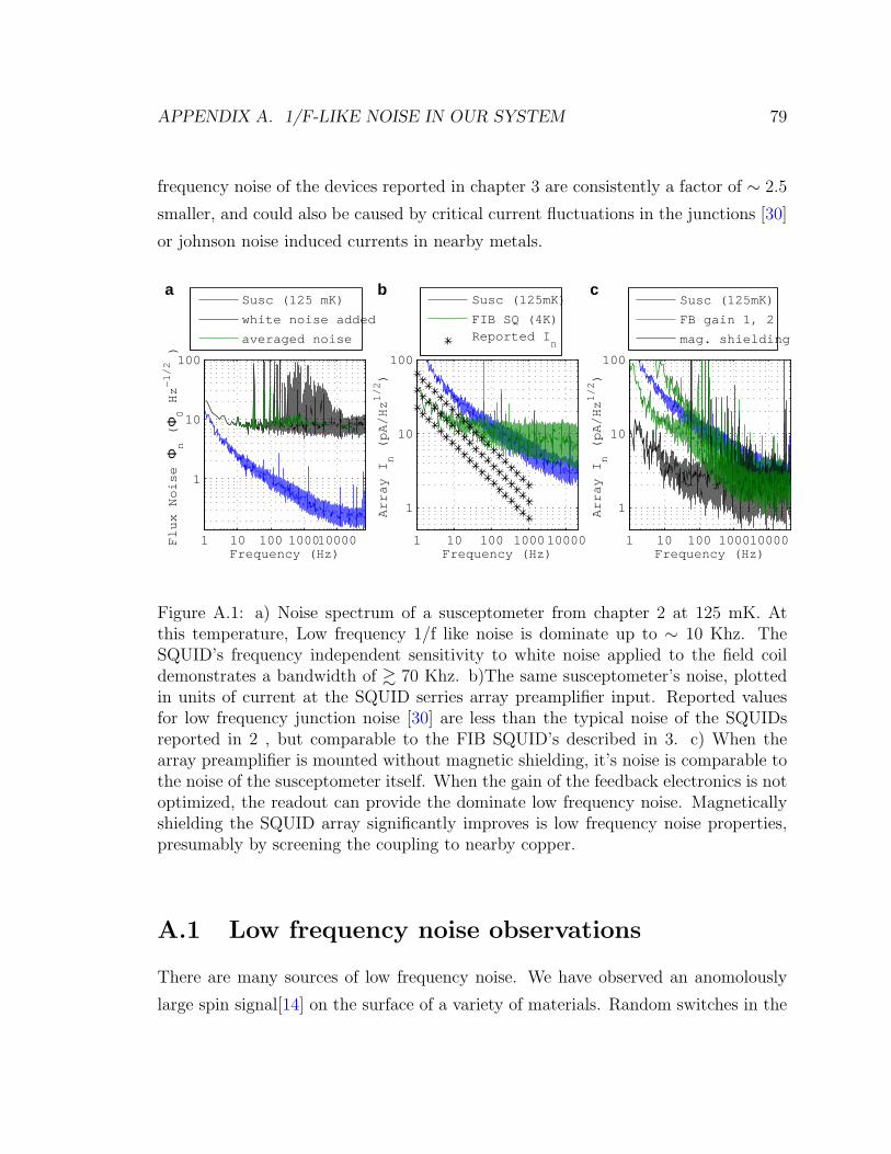
APPENDIX A. 1/F-LIKE NOISE IN OUR SYSTEM 79
frequency noise of the devices reported in chapter 3 are consistently a factor of ∼ 2.5
smaller, and could also be caused by critical current fluctuations in the junctions [30]
or johnson noise induced currents in nearby metals.
1 10 100 100010000
1
10
100
Frequency (Hz)
Flu
x N
ois
e
Φn (
Φ0 H
z−
1/2
)
Susc (125 mK)
white noise added
averaged noise
1 10 100 1000 10000
1
10
100
Frequency (Hz)
Arr
ay
In (
pA
/Hz
1/2
)
Susc (125mK)
FIB SQ (4K)Reported I
n
1 10 100 100010000
1
10
100
Frequency (Hz)
Arr
ay
In (
pA
/Hz
1/2
)
Susc (125mK)
FB gain 1, 2
mag. shielding
a b c
Figure A.1: a) Noise spectrum of a susceptometer from chapter 2 at 125 mK. Atthis temperature, Low frequency 1/f like noise is dominate up to ∼ 10 Khz. TheSQUID’s frequency independent sensitivity to white noise applied to the field coildemonstrates a bandwidth of & 70 Khz. b)The same susceptometer’s noise, plottedin units of current at the SQUID serries array preamplifier input. Reported valuesfor low frequency junction noise [30] are less than the typical noise of the SQUIDsreported in 2 , but comparable to the FIB SQUID’s described in 3. c) When thearray preamplifier is mounted without magnetic shielding, it’s noise is comparable tothe noise of the susceptometer itself. When the gain of the feedback electronics is notoptimized, the readout can provide the dominate low frequency noise. Magneticallyshielding the SQUID array significantly improves is low frequency noise properties,presumably by screening the coupling to nearby copper.
A.1 Low frequency noise observations
There are many sources of low frequency noise. We have observed an anomolously
large spin signal[14] on the surface of a variety of materials. Random switches in the
APPENDIX A. 1/F-LIKE NOISE IN OUR SYSTEM 80
orrientations of these spins could be the source of at least some of the 1/f-like noise
[48] but it is important to rule out other factors.
Critical current fluctuations are often the dominant low-f noise source in Hi-Tc
SQUIDs, but well engineered junctions made from low-Tc materials have less switch-
ing states, and critical current fluctuations are often times not the dominant problem
[21]. Several reported values [30] are shown in figure A.1b. A typical measurement
of a chapter 2 device has a low-f noise above this value. On this generation, we have
also implemented a bias reversal scheme [21], but saw no decrease in low frequency
noise. Thus, we conclude critical current fluctuations do not limit the first generation
of devices. At the time of this writing, bias reversal has not been implemented on the
devices in chapter 3, and the measured reduced value of low-f noise could be explained
by this effect.
Because low-f noise is a ubiquitous problem, it is important to analyze the ampli-
cation stages independently. The measurements reported in figure A.1c were made
in closed loop mode, with the SQUID susceptometer unbiased. Sub-optimal feedback
gain can add additional low-f noise, presumably from the room temperature ICs. In-
dividual 1/f2-like telegraph switchers (plausably from vortex based two-level systems)
can occasionally be seen in the array noise. Magnetical shielding significantly reduces
the low-f noise in the array (Fig. A.1c). This is presumably due to a reduction in the
coupling to normal metal currents, as described in the next section.
A.2 Calculation of low-f noise from nearby metal
We now turn to a method for calculating low frequency noise contribution from john-
son noise induced eddy currents in nearby metals. The approach uses the fasthenry
inductance program [40] to calculate the complex frequency dependent impedance,
Z(ω), of a given susceptometer design. Nearby normal metal contributes a non-zero
frequency-dependent real component to the impedance, which in turn acts as a john-
son noise voltage source, Vn =√
4kBTRe(Z). The corresponding current noise is
In = Vn/|Z|, where most of the impedance is from the reactance |Z| ≈ Im(Z) ≈ iωL,
and the flux noise is Φn = InL.
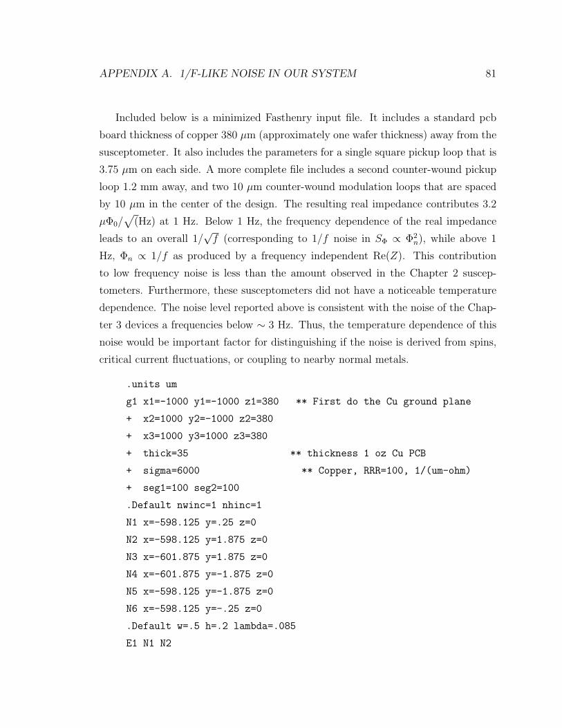
APPENDIX A. 1/F-LIKE NOISE IN OUR SYSTEM 81
Included below is a minimized Fasthenry input file. It includes a standard pcb
board thickness of copper 380 µm (approximately one wafer thickness) away from the
susceptometer. It also includes the parameters for a single square pickup loop that is
3.75 µm on each side. A more complete file includes a second counter-wound pickup
loop 1.2 mm away, and two 10 µm counter-wound modulation loops that are spaced
by 10 µm in the center of the design. The resulting real impedance contributes 3.2
µΦ0/√
(Hz) at 1 Hz. Below 1 Hz, the frequency dependence of the real impedance
leads to an overall 1/√f (corresponding to 1/f noise in SΦ ∝ Φ2
n), while above 1
Hz, Φn ∝ 1/f as produced by a frequency independent Re(Z). This contribution
to low frequency noise is less than the amount observed in the Chapter 2 suscep-
tometers. Furthermore, these susceptometers did not have a noticeable temperature
dependence. The noise level reported above is consistent with the noise of the Chap-
ter 3 devices a frequencies below ∼ 3 Hz. Thus, the temperature dependence of this
noise would be important factor for distinguishing if the noise is derived from spins,
critical current fluctuations, or coupling to nearby normal metals.
.units um
g1 x1=-1000 y1=-1000 z1=380 ** First do the Cu ground plane
+ x2=1000 y2=-1000 z2=380
+ x3=1000 y3=1000 z3=380
+ thick=35 ** thickness 1 oz Cu PCB
+ sigma=6000 ** Copper, RRR=100, 1/(um-ohm)
+ seg1=100 seg2=100
.Default nwinc=1 nhinc=1
N1 x=-598.125 y=.25 z=0
N2 x=-598.125 y=1.875 z=0
N3 x=-601.875 y=1.875 z=0
N4 x=-601.875 y=-1.875 z=0
N5 x=-598.125 y=-1.875 z=0
N6 x=-598.125 y=-.25 z=0
.Default w=.5 h=.2 lambda=.085
E1 N1 N2
APPENDIX A. 1/F-LIKE NOISE IN OUR SYSTEM 82
E2 N2 N3
E3 N3 N4
E4 N4 N5
E5 N5 N6
.external N1 Nf
.freq fmin=0.159155 fmax=1.59155 ndec=0.01
.end
Appendix B
Concepts for future scanning
SQUID designs
Nicholas C. Koshnick, John R. Kirtley, Kathryn A. Moler
An early paper draft intended for submission to Superconductor Science and Tech-
nology
Abstract
In this paper we discuss design concepts for decreasing the spatial resolution, improv-
ing the sensitivity and reducing the invasiveness in scanning Superconducting Quan-
tum Interference Device (SQUID) microscope sensors with integrated flux pickup
loops. This can be done not only by reducing the ground-rule line widths and spac-
ings, but also by taking advantage of planarization, reducing flux noise through re-
ducing the SQUID inductance, and reducing back-action through dispersive readouts
or on-chip filtering.
83
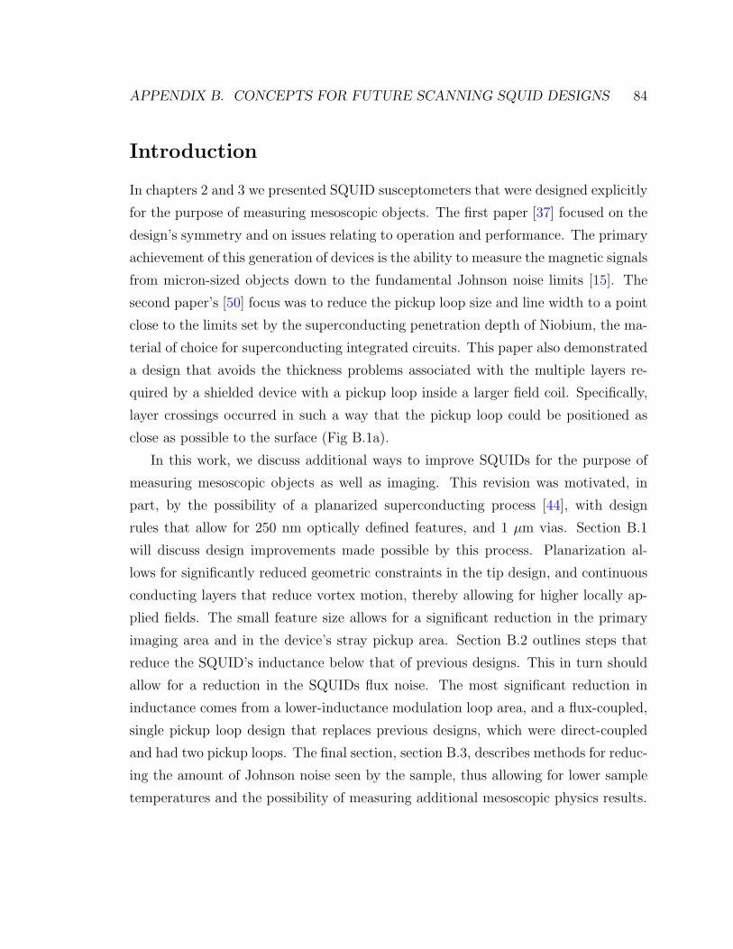
APPENDIX B. CONCEPTS FOR FUTURE SCANNING SQUID DESIGNS 84
Introduction
In chapters 2 and 3 we presented SQUID susceptometers that were designed explicitly
for the purpose of measuring mesoscopic objects. The first paper [37] focused on the
design’s symmetry and on issues relating to operation and performance. The primary
achievement of this generation of devices is the ability to measure the magnetic signals
from micron-sized objects down to the fundamental Johnson noise limits [15]. The
second paper’s [50] focus was to reduce the pickup loop size and line width to a point
close to the limits set by the superconducting penetration depth of Niobium, the ma-
terial of choice for superconducting integrated circuits. This paper also demonstrated
a design that avoids the thickness problems associated with the multiple layers re-
quired by a shielded device with a pickup loop inside a larger field coil. Specifically,
layer crossings occurred in such a way that the pickup loop could be positioned as
close as possible to the surface (Fig B.1a).
In this work, we discuss additional ways to improve SQUIDs for the purpose of
measuring mesoscopic objects as well as imaging. This revision was motivated, in
part, by the possibility of a planarized superconducting process [44], with design
rules that allow for 250 nm optically defined features, and 1 µm vias. Section B.1
will discuss design improvements made possible by this process. Planarization al-
lows for significantly reduced geometric constraints in the tip design, and continuous
conducting layers that reduce vortex motion, thereby allowing for higher locally ap-
plied fields. The small feature size allows for a significant reduction in the primary
imaging area and in the device’s stray pickup area. Section B.2 outlines steps that
reduce the SQUID’s inductance below that of previous designs. This in turn should
allow for a reduction in the SQUIDs flux noise. The most significant reduction in
inductance comes from a lower-inductance modulation loop area, and a flux-coupled,
single pickup loop design that replaces previous designs, which were direct-coupled
and had two pickup loops. The final section, section B.3, describes methods for reduc-
ing the amount of Johnson noise seen by the sample, thus allowing for lower sample
temperatures and the possibility of measuring additional mesoscopic physics results.
APPENDIX B. CONCEPTS FOR FUTURE SCANNING SQUID DESIGNS 85
B.1 Advantages of a planarized device with multi-
layer sub-micron features
The thickness of superconducting layers in an integrated process is constrained to
be larger than the superconducting penetration depth. Layers thinner than this have
limited field screening abilities and narrow, thin features can have a non-negligible ki-
netic inductance. To avoid these potential problems, superconducting foundries post
design rules with layers thicknesses between 150 and 200 nm, substantially greater
than the ≈ 85 nm penetration depth of sputtered Niobium. Given the thickness of
individual layers, it is difficult to design sub-micron features into a multi-layered ar-
chitecture, because small features cannot be reliably fabricated when the underlying
height profile varies on the same length scale. It is therefore reasonable to con-
clude that any new superconducting foundry that utilizes the now readily available
sub-micron lithography tools, will also likely choose to adopt chemical-mechanical
polishing steps after each conductor/insulator layer.
The adoption of a planarization process would considerably reduce the geometric
constraints that determine whether the pickup loop layer will touch down first. Our
previous paper [50] described the use of a shallow etch outside the pickup loop and
a deep etch outside the field coil. This geometry, shown in the layer diagram in
Fig. B.1a, can allow a top-layer pickup loop to touch down first with an alignment
tolerance of 3 degrees. Such alignment tolerance is necessary because of the limited
alignment ability in home-built scanners and because changes after alignment due to
thermal contractions. With a planarized process, a minimum alignment angle is no
longer inherent in the design. This means a larger tolerance angle can be achieved
(Fig B.1b,c,), or a wider field coil can be used, which has the potential of increasing
the maximum usable applied field.
Another very important geometric advantage of a planarized design is that the via
to a top layer pickup loop can be much closer to the pickup loop itself, which would
allow for a smaller imaging kernel. In the design shown in Fig B.1a, the electrical
connection to the top layer is more than 15 µm from the touch down point. Although
the magnetic field seen by the pickup loop leads (in layer W2) is partially screened
APPENDIX B. CONCEPTS FOR FUTURE SCANNING SQUID DESIGNS 86
Deep
RIE
Deep
RIE
RIE
Deep
RIE
(a)
(c)
(e)
(d)
(f )
(b)
5 µm
10 µm
5 µm
Figure B.1: (Color Online) Comparison of design layouts and layer considerations fora planarized vs. a non-planarized design with sub-micron feature sizes. (a-c) Cross-sections down the the center line of the design showing layer thickness effects. (a)Layer thicknesses of a non planarized process described elsewhere [50], with three su-perconducting layers (BE, W1, W2), two insulating layers (I1, I2), and the substrate.Atomic force microscope data (blue) shows the tolerance angles that would allow atop layer FIB fabricated pickup loop to touch first. (b) The layer thicknesses of aplanarized design allow for much shorter pickup loop leads with the same toleranceangles. (c) The layer thickness diagram of a middle layer pickup loop design. (d-f)Top down view of SQUID design. (d) Passing the field coil under the linear coaxsection of the SQUID leads allows for a symmetric tip. (e) The mid-layer pickup loopdesign shown in (c). (f) The top layer design shown in (b).
APPENDIX B. CONCEPTS FOR FUTURE SCANNING SQUID DESIGNS 87
by the middle layer (W1), the long leads still make for a large area where the SQUID
is responsive to the sample’s magnetic field. In a planarized design, the vias can be
brought as close as is allowed by the design rules.
In previous papers we have demonstrated how susceptometry and background
cancellations can enable Johnson noise limited detection of magnetic signals from
mesoscopic samples such as superconducting and normal metal rings. Such objects
can have periodic response due to quantum mechanical effects, where the amplitude of
this response is inversely related to the ring size. The minimum ring size is set by the
applied field, because at least half a flux quantum of field is required to distinguish a
periodic signal from an (often much larger) linear signal related to spins. Furthermore,
we have found that if the field is not sourced by the local field coils, then coupling
into the SQUID modulation loop, SQUID array amplifier, and additional vibration-
related signals severely reduce the technique’s sensitivity. Increasing the width and
thickness of the field coil loop is not enough to increase the usable maximum applied
field. We have found that these measures increase the field coil current that makes
the SQUID go normal, but that sensitivity is no longer optimal once vortices begin to
move at a much lower field [50]. Planarization also allows for continuous conducting
layers, which reduces thin superconducting areas in the design, and thus should also
help to reduce the field coil current where vortices begin to move.
Spatial resolution is an important factor of a SQUID’s design for many reasons.
In the large set of cases where it is acceptable have the pickup loop ' 300 nm from
the sample, it is advantageous to put the pickup loop in the middle layer as shown
in Figs. B.1c-e. This allows for a minimal image kernel size, because both the top
and bottom layers can screen the pickup loop from magnetic field. The width of
the shielding layers has been kept to a minimum in the area immediately before the
pickup loop to minimize the flux-focusing effects that can increase the effective pickup
loop size [42].
Our design for a SQUID with a pickup loop in the top layer, Fig. B.1f, is similar
to that of Fig. B.1e, except that the flux-focusing condition was relaxed to allow for
shorter leads and thus less stray coupling. Both designs have a field coil line that
APPENDIX B. CONCEPTS FOR FUTURE SCANNING SQUID DESIGNS 88
crosses far behind the pickup loop area in a region where the SQUID has a linear coax-
ial geometry, Fig. B.1d. This allows for a symmetric tip, minimal unshielded leads,
and thus a pickup and transition area that contributes minimally to the inductance
of the rest of the design.
B.2 Optimizing flux sensitivity through reduced
inductance
While table 3.1 demonstrates that the flux sensitivity of our SQUIDs is comparable
to or better than scanning devices of its kind, quantum-limited devices [21] with flux
sensitivities as low as ∼ 0.08µΦ0/√Hz [5] have been realized. Referring back to Fig.
3.5, we note that our designs are limited by thermal noise in the shunt resistors.
When optimally tuned, this Johnson noise dependence scales like L3/2 where L is the
SQUID’s self inductance [79]. The quantum limited flux noise has a L1/2 dependence
when optimally tuned. By reducing L one can both reduce the SQUID’s overall white
noise floor, and increase the temperature, where temperature-independent quantum
noise becomes the dominate noise source.
For both the optically [37] and FIB [50] fabricated SQUIDs, the inductance [40] of
each section is approximately 12 pH per pickup loop, 10 pH/mm in the linear coaxial
connection region, and ∼ 55 pH for the core junction/modulation loop area.
The majority of the core area inductance in the previous designs come from the
two modulation loops, each with an inner diameter of 10 µm. Estimating from their
inner diameter [39], these two loops contribute 30 pH to the total inductance. This
contribution would decrease linearly with a reduction in the diameter of the loop.
The main drawback to this in our case (low bandwidth requirements) is that more
current is required to keep the SQUID in a flux-locked loop. Increases in the amount
of current sent to the modulation loops can lead to heating from stray resistances
in dilution refrigerator temperature wiring. Reducing the modulation loop diameter
to 4 µm decreases the self inductance to 12 pH, while maintaining a reasonable 175
uA/phi0 mutual inductance. Further enhancement could come from having only one
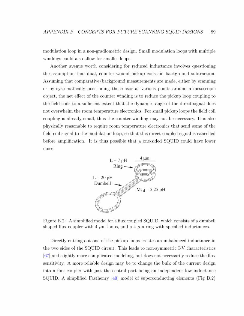
APPENDIX B. CONCEPTS FOR FUTURE SCANNING SQUID DESIGNS 89
modulation loop in a non-gradiometric design. Small modulation loops with multiple
windings could also allow for smaller loops.
Another avenue worth considering for reduced inductance involves questioning
the assumption that dual, counter wound pickup coils aid background subtraction.
Assuming that comparative/background measurements are made, either by scanning
or by systematically positioning the sensor at various points around a mesoscopic
object, the net effect of the counter winding is to reduce the pickup loop coupling to
the field coils to a sufficient extent that the dynamic range of the direct signal does
not overwhelm the room temperature electronics. For small pickup loops the field coil
coupling is already small, thus the counter-winding may not be necessary. It is also
physically reasonable to require room temperature electronics that send some of the
field coil signal to the modulation loop, so that this direct coupled signal is cancelled
before amplification. It is thus possible that a one-sided SQUID could have lower
noise.
4 µm
Mr-d = 5.25 pH
L = 7 pH Ring
L = 20 pHDumbell
Figure B.2: A simplified model for a flux coupled SQUID, which consists of a dumbellshaped flux coupler with 4 µm loops, and a 4 µm ring with specified inductances.
Directly cutting out one of the pickup loops creates an unbalanced inductance in
the two sides of the SQUID circuit. This leads to non-symmetric I-V characteristics
[67] and slightly more complicated modeling, but does not necessarily reduce the flux
sensitivity. A more reliable design may be to change the bulk of the current design
into a flux coupler with just the central part being an independent low-inductance
SQUID. A simplified Fasthenry [40] model of superconducting elements (Fig B.2)
APPENDIX B. CONCEPTS FOR FUTURE SCANNING SQUID DESIGNS 90
illustrates the tradeoffs between the reduced coupling to the sample, and the reduction
in the SQUID’s inductance. It considers the inductances of two objects: a simple 4
µm diameter ring, and a “dumbell” consisting of two 4 µm diameter loops coupled
by two lines. This dumbell object has a self inductance, Ld = 20 pH, and can
be considered either as a direct coupled SQUID or the flux coupler that is coupled
to the ring. In the latter case, the ring, which has a self inductance Lr = 7 pH,
represents the non-directly coupled SQUID. The mutual inductance between the ring
and dumbell is Mr−d = 5.25 pH. The flux-coupled SQUID only sees Mr−d/Ld = .26
as much flux as its direct-coupled counterpart, but when limited by Johnson noise, it
has (Lr/Ld)3/2 = .21 as much white noise. Flux-coupled and direct-coupled SQUIDs
therefore have very similar white noise characteristics until the inductance is small
enough that the L1/2-dependent quantum limit is applicable. The main advantage
may be that a flux-coupled SQUID could have only one pickup loop, substantially
reducing the inductance without leaving the SQUID unbalanced.
B.3 Reducing SQUID sample back action
Understanding the way the SQUID perturbs the sample is an important part of
measuring quantum effects in mesoscopic samples. We will consider one of the sim-
plest kinds of back action on the sample, joule heating from SQUID radiation at the
Josephson frequency, fj. While studying persistent currents in normal metal rings,
we discovered that metallic regions had a spin-like linear susceptibility that increased
with decreasing temperature. The coupled SQUID radiation of ≈ 10−14 Watts for our
≈ 2Ω rings, balanced by electron-phonon limited cooling [85], limited the temperature
in isolated rings to about 200 mK [15]. Since there are many interesting effects that
only occur below this temperature, it is important to consider design aspects that
can reduce this form of back action.
In general, the cost of reduced back-action is often reduced sensitivity. A simple
estimate for the energy dissipated in a ring is given by the flux-change-induced ring-
voltage
Vring =dΦ
dt= I0fjMSQ−s (B.1)
APPENDIX B. CONCEPTS FOR FUTURE SCANNING SQUID DESIGNS 91
where MSQ−s is the mutual inductance between the SQUID and the sample. The
power dissipated is then just V 2ring/R, where R is the ring’s resistance. One can
reduce this heating effect by moving the SQUID further away from the sample, thereby
reducing MSQ−s. This is only a useful approach when there is ample signal. Another
approach is to bias the SQUID with the lowest possible voltage, and thus lowest
operating fj. In general, this approach is limited by the minimum voltage bias (∝kBT/e), where the SQUID noise begins to deteriorate, and by the feedback electronics’
ability to lock into a signal that has a reduced modulation amplitude.
The noise dependance on L3/2, mentioned in section B.2, was calculated in the
βL = 2LI0/Φ0 ≈ 1 limit, where the standard design rules [79] set critical current to
I0 = Φ0/2L, and the appropriate shunt resistor is determined by βc ≈ 1. Increasing
the flux sensitivity by reducing L thus comes with an increased I0 and correspondingly
increased radiation on the sample. While the SQUID’s energy sensitivity, Φ2n/L, is
optimal for βL ≈ 1, the relevant figure of merit when measuring mesoscopic samples
must include back action. The optimal point in this case would probably require
I0 < Φ0/2L. This effect has been analyzed in quantum limited SQUIDs [24].
Another way to reduce the back action on the sample is to read out the the SQUID
dispersively. Josephson radiation (and thus sample heating) does not occur when the
SQUID is in the zero voltage state. Dispersive readout measures the flux-dependence
of the inductance, without inducing voltage, typically by placing the SQUID in some
kind of resonant circuit. Thus the Josephson radiation (of typically 1-10 GHz) gets
replaced by the readout frequency (∼ 100 Mhz). One excellent way to implement
dispersive readout involves the microstrip SQUID amplifier designed by the group of
John Clarke [65]. The superconducting qubit community has invested considerable
effort in comparing the back action from this type of measurement to the back action
from other non-voltage state readout schemes, such as the scanning SQUIDs [32] that
rely on the bias current switching threshold.
A final way to limit SQUID heating would be to implement on-chip filters inside
the SQUID circuit that divert the Josephson frequency currents from the pickup loop
and sample. This approach was implemented with LC filters by John Price’s group
[90] in a two-chip design. Implementing the same type of LC filters on a single chip
APPENDIX B. CONCEPTS FOR FUTURE SCANNING SQUID DESIGNS 92
would help to keep inductive losses to a minimum. We estimate the feasibility of this
approach by noting the capacitance in our 40 µm wide, 1.2 mm long linear coaxial
coupler with a 200 nm wire-to-wire spacing is roughly 20 pF. The 30 pH pickup loop
and strip line inductance thus has a cutoff frequency of 6.5 Ghz, indicating that a
reasonable portion of the Josephson frequency current is already not flowing through
the pickup loop itself. The radiation from the SQUID would be further decoupled
from the sample if the on-chip capacitance was further increased.
A second type of on-chip filter involves placing a placing a small ( 0.3 Ω) shunting
resistor between the SQUID and the pickup loop. This form of an RC filter works
as a frequency dependent current divider, where the Josephson frequency currents
would see a reactance of 0.95 Ω (15 pH at ∼ 10 Ghz) and thus largely run through
the shunt, whereas the zero frequency currents that set up the SQUID phase relations
would still all be coupled to the pickup loop itself.
As with the LC filter technique, this logic intrinsically relies on the fact that we
are trying to measure time-averaged equilibrium currents in our rings, and thus can
simply limit the frequencies where effective coupling occurs to some value below the
frequencies involved with the intrinsic SQUID (or for that mater, ring) dynamics.
The LC filter could effectively shunt essentially all of the Josephson frequency radi-
ation if such an ideal capacitor layer, with sufficiently low stray inductance, could
be incorporated into the superconducting process. The effectiveness of the RC filter
is limited by the Johnson current noise it sends through the pickup loop, integrated
up to the bandwidth set by the LC filter. In practice, however, it is likely that this
RC shunting technique could reduce the sample temperature significantly before this
limit sets in.
Bibliography
[1] Attocube Systems AG.
[2] An Aug.-Sep. 2008 ring cool down intended to provide extra data for the phase
fluctuations discussed in chapter 5.
[3] V. Ambegaokar and U. Eckern. Nonlinear diamagnetic response in mesoscopic
rings of superconductors above tsub c. Europhys. Lett., 13(8):733 – 8, Dec 1990.
[4] A. Anthore, H. Pothier, and D. Esteve. Density of states in a superconductor
carrying a supercurrent. Physical Review Letters, 90(12):127001, March 2003.
[5] D. D. Awschalom, J. R. Rozen, M. B. Ketchen, W. J. Gallagher, A. W. Klein-
sasser, R. L. Sandstrom, and B. Bumble. Low-noise modular microsusceptometer
using nearly quantum limited dc squids. Applied Physics Letters, 53(21):2108–
2110, November 1988.
[6] D. D. Awschalom, J. Warnock, and S. Vonmolnar. Low-temperature mag-
netic spectroscopy of a dilute magnetic semiconductor. Physical Review Letters,
58(8):812 – 15, FEB 1987.
[7] J. G. Bednorz and K. A. Muller. Possible high tc superconductivity in the ba-
la-cu-o system. Zeitschrift fur Physik B Condensed Matter, 64(2):189–193, June
1986.
[8] Jorge Berger. Ginzburg-landau equations with consistent langevin terms for
nonuniform wires. Phys. Rev. B, 75(18):184522, 2007.
93
BIBLIOGRAPHY 94
[9] Jorge Berger and Jacob Rubinstein. Topology of the order parameter in the
little-parks experiment. Phys. Rev. Lett., 75(2):320–322, Jul 1995.
[10] Alexey Bezryadin. Quantum suppression of superconductivity in nanowires.
Journal of Physics: Condensed Matter, 20:043202, 2008.
[11] P. G. Bjornsson, B. W. Gardner, J. R. Kirtley, and K. A. Moler. Scanning su-
perconducting quantum interference device microscope in a dilution refrigerator.
Rev. Sci. Inst., 72(11):4153 – 8, NOV 2001.
[12] P. G. Bjornsson, Y. Maeno, M. E. Huber, and K. A. Moler. Scanning magnetic
imaging of srsub 2ruosub 4. Physical Review B (Condensed Matter and Materials
Physics), 72(1):12504 – 1, 2005.
[13] Ania Bleszynski and Jack Harris. (unpublished).
[14] H. Bluhm, N. C. Koshnick, J.A. Bert, M. E. Huber, and K. A. Moler. Spin-like
susceptibility of metallic and insulating thin films at low temperature. (unpub-
lished).
[15] Hendrik Bluhm, Nicholas C Koshnick, Julie A Bert, Martin E Hu-
ber, and Kathryn A Moler. Persistent currents in normal metal rings.
arXiv.org:0810.4384, October 2008. Accepted for publication in Physical Re-
view Letters.
[16] Hendrik Bluhm, Nicholas C. Koshnick, Martin E. Huber, and Kathryn A. Moler.
Magnetic response of mesoscopic superconducting rings with two order parame-
ters. Physical Review Letters, 97:237002–4, December 2006.
[17] Hendrik Bluhm, Nicholas C Koshnick, Martin E Huber, and Kathryn A
Moler. Multiple fluxoid transitions in mesoscopic superconducting rings.
arXiv.org:0709.1175, September 2007.
[18] Ernst Helmut Brandt and John R. Clem. Superconducting thin rings with finite
penetration depth. Physical Review B, 69:184509, May 2004.
BIBLIOGRAPHY 95
[19] N. Byers and C. N. Yang. Theoretical considerations concerning quantized mag-
netic flux in superconducting cylinders. Phys. Rev. Lett., 7(2):46–49, Jul 1961.
[20] J. A. Chervenak, F. M. Finkbeiner, T. R. Stevenson, D. J. Talley, R. P. Brekosky,
S. R. Bandler, E. Figueroa-Feliciano, M. A. Lindeman, R. L. Kelley, T. Saab, and
C. K. Stahle. Fabrication of transition edge sensor x-ray microcalorimeters for
constellation-x. Nuclear Instruments and Methods in Physics Research Section A:
Accelerators, Spectrometers, Detectors and Associated Equipment, 520(1-3):460–
462, March 2004.
[21] J. Clarke and A. I. Braginski, editors. The SQUID Handbook. Weinheim : Wiley-
VCH, 2003.
[22] J.-P. Cleuziou, W. Wernsdorfer, V. Bouchiat, T. Ondarcuhu, and M. Monthioux.
Carbon nanotube superconducting quantum interference device. Nat Nano, 1:53–
59, October 2006.
[23] Roger W. Cohen and B. Abeles. Superconductivity in granular aluminum films.
Physical Review, 168(2):444, April 1968.
[24] V. Danilov, K. Likharev, and A. Zorin. Quantum noise in squids. Magnetics,
IEEE Transactions on, 19(3):572–575, 1983.
[25] M. Daumens, C. Meyers, and A. Buzdin. Little-parks effect for arbitrary geom-
etry: fluctuations of the magnetic moment of mesoscopic loops. Physics Letters
A, 248:445–452, Nov 1998.
[26] V.J. Emery and S.A. Kivelson. Importance of phase fluctuations in supercon-
ductors with small superfluid density. Nature, 374:434–437, March 1995.
[27] M. Freitag, J.C. Tsang, J. Kirtley, A. Carlsen, J. Chen, A. Troeman,
H. Hilgenkamp, and Ph. Avouris. Electrically excited, localized infrared emission
from single carbon nanotubes. Nano Letters, 6:1425–1433, July 2006.
BIBLIOGRAPHY 96
[28] Brian W. Gardner, Janice C. Wynn, Per G. Bjornsson, Eric W. J. Straver,
Kathryn A. Moler, John R. Kirtley, and Mark B. Ketchen. Scanning supercon-
ducting quantum interference device susceptometry. Review of Scientific Instru-
ments, 72(5):2361–2364, 2001.
[29] N. Giordano. Evidence for macroscopic quantum tunneling in one-dimensional
superconductors. Physical Review Letters, 61:2137, October 1988.
[30] D. J. Van Harlingen, T. L. Robertson, B. L. T. Plourde, P. A. Reichardt,
T. A. Crane, and John Clarke. Decoherence in josephson-junction qubits due to
critical-current fluctuations. Physical Review B, 70(6):064517, 2004.
[31] K. Hasselbach, D. Mailly, and J. R. Kirtley. Micro-superconducting quantum
interference device characteristics. Journal of Applied Physics, 91:4432–4437,
April 2002.
[32] K. Hasselbach, C. Veauvy, and D. Mailly. Microsquid magnetometry and mag-
netic imaging. Physica C, 332:140–147, May 2000.
[33] M. Hayashi and H. Ebisawa. Superconducting fluctuations in a mesoscopic ring
structure: Little-Parks oscillation in fluctuation regime. Physica C Superconduc-
tivity, 352:191–194, April 2001.
[34] G.C. Hilton, J.M. Martinis, K.D. Irwin, N.F. Bergren, D.A. Wollman, M.E. Hu-
ber, S. Deiker, and S.W. Nam. Microfabricated transition-edge x-ray detectors.
Applied Superconductivity, IEEE Transactions on, 11(1):739–742, 2001.
[35] Gene C. Hilton, John M. Martinis, Kent D. Irwin, and David A. Wollman.
Normal metal boundary conditions for multi-layer tes detectors, September 2002.
U.S. Patent Classification: 250/336.2 ; International Classification: H01L 3900.
[36] M. E. Huber, P. A. Neil, R. G. Benson, D. A. Burns, A. F. Corey, C. S. Flynn,
Y. Kitaygorodskaya, O. Massihzadeh, J. M. Martinis, and G. C. Hilton. Dc squid
series array amplifiers with 120 mhz bandwidth (corrected). Applied Supercon-
ductivity, IEEE Transactions on, 11(2):4048–4053, 2001.
BIBLIOGRAPHY 97
[37] Martin E. Huber, Nicholas C. Koshnick, Hendrik Bluhm, Leonard J. Archuleta,
Tommy Azua, Per G. Bjornsson, Brian W. Gardner, Sean T. Halloran, Erik A.
Lucero, and Kathryn A. Moler. Gradiometric micro-squid susceptometer for
scanning measurements of mesoscopic samples. Review of Scientific Instruments,
79(5):053704, 2008.
[38] K. D. Irwin, G. C. Hilton, John M. Martinis, S. Deiker, N. Bergren, S. W. Nam,
D. A. Rudman, and D. A. Wollman. A mo-cu superconducting transition-edge
microcalorimeter with 4.5ev energy resolution at 6kev. Nuclear Instruments and
Methods in Physics Research Section A: Accelerators, Spectrometers, Detectors
and Associated Equipment, 444(1-2):184–187, April 2000.
[39] J. Jaycox and M. Ketchen. Planar coupling scheme for ultra low noise DC
SQUIDs. Magnetics, IEEE Transactions on, 17(1):400–403, 1981.
[40] M. Kamon, M. J. Tsuk, and J. K. White. Fasthenry: a multipole-accelerated
3-d inductance extraction program. IEEE Transactions on Microwave Theory
and Techniques, 42(9):1750 – 1758, Sept 1994.
[41] M. B. Ketchen and J. R. Kirtley. Design and performance aspects of pickup loop
structures for miniature squid magnetometry. IEEE Transactions on Applied
Superconductivity, 5(2):2133 – 2136, Jun 1995.
[42] M. B. Ketchen and J. R. Kirtley. Design and performance aspects of pickup loop
structures for miniature squid magnetometry. IEEE Transactions on Applied
Superconductivity, 5(2):2133 – 2136, Jun 1995.
[43] M. B. Ketchen, T. Kopley, and H. Ling. Miniature squid susceptometer. Applied
Physics Letters, 44(10):1008 – 10, May 1984.
[44] M. B. Ketchen, D. Pearson, A. W. Kleinsasser, C.-K. Hu, M. Smyth, J. Logan,
K. Stawiasz, E. Baran, M. Jaso, T. Ross, K. Petrillo, M. Manny, S. Basava-
iah, S. Brodsky, S. B. Kaplan, W. J. Gallagher, and M. Bhushan. Sub-mu m,
BIBLIOGRAPHY 98
planarized, Nb-AlOx -Nb josephson process for 125 mm wafers developed in part-
nership with si technology. Applied Physics Letters, 59(20):2609–2611, November
1991.
[45] M.B. Ketchen, D.D. Awschalom, W.J. Gallagher, A.W. Kleinsasser, R.L. Sand-
strom, J.R. Rozen, and B. Bumble. Design, fabrication, and performance of
integrated miniature squid susceptometers. Magnetics, IEEE Transactions on,
25:1212–1215, 1989.
[46] J. R. Kirtley, M. B. Ketchen, K. G. Stawiasz, J. Z. Sun, W. J. Gallagher, S. H.
Blanton, and S. J. Wind. High-resolution scanning squid microscope. Applied
Physics Letters, 66:1138–1140, February 1995.
[47] John R. Kirtley and John P. Wikswo. Scanning squid microscopy. Annual Review
of Materials Science, 29(1):117–148, 1999.
[48] Roger H. Koch, David P. DiVincenzo, and John Clarke. Model for 1/f flux noise
in squids and qubits. Physical Review Letters, 98(26):267003–4, June 2007.
[49] Nicholas C. Koshnick, Hendrik Bluhm, Martin E. Huber, and Kathryn A. Moler.
Fluctuation superconductivity in mesoscopic aluminum rings. Science, 318:1440–
1443, November 2007.
[50] Nicholas C. Koshnick, Martin E. Huber, Julie A. Bert, Clifford W. Hicks, Jeff
Large, Hal Edwards, and Kathryn A. Moler. A terraced scanning superconduct-
ing quantum interference device susceptometer with submicron pickup loops.
Applied Physics Letters, 93(24):243101–3, December 2008.
[51] J M Kosterlitz and D J Thouless. Ordering, metastability and phase transi-
tions in two-dimensional systems. Journal of Physics C: Solid State Physics,
6(7):1181–1203, 1973.
[52] S. K. H. Lam and D. L. Tilbrook. Development of a niobium nanosupercon-
ducting quantum interference device for the detection of small spin populations.
Applied Physics Letters, 82(7):1078–1080, 2003.
BIBLIOGRAPHY 99
[53] J. S. Langer and Vinay Ambegaokar. Intrinsic resistive transition in narrow
superconducting channels. Phys. Rev., 164(2):498–510, Dec 1967.
[54] A. Larkin and A. A. Varlamov. Theory of Fluctuations in Superconductors.
Oxford University Press, USA, 2005.
[55] C. N. Lau, N. Markovic, M. Bockrath, A. Bezryadin, and M. Tinkham. Quantum
phase slips in superconducting nanowires. Phys. Rev. Lett., 87(21):217003, Nov
2001.
[56] W. A. Little and R. D. Parks. Observation of quantum periodicity in the tran-
sition temperature of a superconducting cylinder. Phys. Rev. Lett., 9(1):9, Jul
1962.
[57] Y. Liu, H. Wang, Yu. Zadorozhny, M.M. Rosario, B.Y. Rock, N.A. Kurz, and
P.T. Carrigan. Ultrathin, doubly connected superconducting cylinders: A link
between one- and two-dimensional superconductors. Physica C: Superconductiv-
ity, 468(4):331–336, February 2008.
[58] Y. Liu, Yu. Zadorozhny, M. M. Rosario, B. Y. Rock, P. T. Carrigan, and
H. Wang. Destruction of the Global Phase Coherence in Ultrathin, Doubly
Connected Superconducting Cylinders. Science, 294(5550):2332–2334, 2001.
[59] D. Mailly, C. Chapelier, and A. Benoit. Experimental observation of persistent
currents in gaas-algaas single loop. Physical Review Letters, 70(13):2020, March
1993.
[60] J. B. Majer, J. R. Butcher, and J. E. Mooij. Simple phase bias for supercon-
ducting circuits. Applied Physics Letters, 80:3638–3640, 2002.
[61] J. Martinis. personal communication, 2008.
[62] K. A. Matveev, A. I. Larkin, and L. I. Glazman. Persistent current in su-
perconducting nanorings. Physical Review Letters, 89(9):096802, 2002. Copy-
right (C) 2009 The American Physical Society; Please report any problems to
BIBLIOGRAPHY 100
[63] D. E. McCumber and B. I. Halperin. Time scale of intrinsic resistive fluctuations
in thin superconducting wires. Phys. Rev. B, 1(3):1054–1070, Feb 1970.
[64] Toshimitsu Morooka, Keiichi Tanaka, Akikazu Odawara, Satoshi Nakayama, At-
sushi Nagata, Masanori Ikeda, and Kazuo Chinone. Development of scanning
squid microscope for studying superconducting films and devices. Physica C,
335:157–163, June 2000.
[65] Michael Muck, J. B. Kycia, and John Clarke. Superconducting quantum inter-
ference device as a near-quantum-limited amplifier at 0.5 ghz. Applied Physics
Letters, 78(7):967–969, February 2001.
[66] G. O’Neil, D. Schmidt, N. A. Miller, J. N. Ullom, A. Williams, G. B. Arnold,
and S. T. Ruggiero. Observation of nonmagnetic resonant scattering effects
by tunneling in dilute al-mn alloy superconductors. Physical Review Letters,
100(5):056804–4, February 2008.
[67] R. L. Peterson and C. A. Hamilton. Analysis of threshold curves for supercon-
ducting interferometers. Journal of Applied Physics, 50:8135–8142, December
1979.
[68] Richard B. Pettit and J. Silcox. Film structure and enhanced superconductivity
in evaporated aluminum films. Physical Review B, 13(7):2865, April 1976.
[69] T. M. Rice. Superconductivity in one and two dimensions. Phys. Rev.,
140(6A):A1889–A1891, Dec 1965.
[70] Eberhard K. Riedel and Felix von Oppen. Mesoscopic persistent current in small
rings. Physical Review B, 47(23):15449, June 1993.
[71] M. M. Rosario, Y. Zadorozhny, B. Y. Rock, P. T. Carrigan, H. Wang, and
Y. Liu. Superconducting fluctuations in the destructive regime of ultrathin,
superconducting cylinders. Physica B Condensed Matter, 329:1415–1416, May
2003.
BIBLIOGRAPHY 101
[72] J.E. Sauvageau, C.J. Burroughs, P.A.A. Booi, M.W. Cromar, R.P. Benz, and
J.A. Koch. Superconducting integrated circuit fabrication with low temperature
ecr-based pecvd sio2 dielectric films. Applied Superconductivity, IEEE Transac-
tions on, 5:2303–2309, 1995.
[73] D. J. Scalapino, M. Sears, and R. A. Ferrell. Statistical mechanics of one-
dimensional ginzburg-landau fields. Phys. Rev. B, 6(9):3409–3416, Nov 1972.
[74] D. R. Schmidt, K. W. Lehnert, A. M. Clark, W. D. Duncan, K. D. Irwin,
N. Miller, and J. N. Ullom. A superconductor–insulator–normal metal bolometer
with microwave readout suitable for large-format arrays. Applied Physics Letters,
86(5):053505–3, 2005.
[75] G. Schwiete. personal communication, 2007.
[76] Georg Schwiete and Yuval Oreg. Persistent current in small superconducting
rings. arXiv.org:0812.4088, December 2008.
[77] J. Siegel, J. Witt, N. Venturi, and S. Field. Compact large-range cryogenic
scanner. Review of Scientific Instruments, 66(3):2520 – 3, MAR 1995.
[78] B. Spivak, P. Oreto, and S. A. Kivelson. Theory of quantum metal to supercon-
ductor transitions in highly conducting systems. Physical Review B (Condensed
Matter and Materials Physics), 77(21):214523–18, June 2008.
[79] Claudia D. Tesche and John Clarke. dc squid: Noise and optimization. Journal
of Low Temperature Physics, 29:301–331, November 1977.
[80] Claudia D. Tesche and John Clarket. dc squid: Current noise. Journal of Low
Temperature Physics, 37(3):397–403, November 1979.
[81] A.G.P. Troeman, H. Derking, B. Borger, J. Pleikies, D. Veldhuis, and
H. Hilgenkamp. Nanosquids based on niobium constrictions. Nano Letters,
7:2152–2156, July 2007.
BIBLIOGRAPHY 102
[82] Oskar Vafek, M. R Beasley, and Steven A Kivelson. Disorder induced
non-fermi liquid near a metal-superconductor quantum phase transition.
arXiv.org:0505688, May 2005.
[83] F. von Oppen and E. K. Riedel. Flux-periodic persistent current in mesoscopic
superconducting rings close to tsub c. Phys. Rev. B, 46(5):3203 – 6, AUG 1992.
[84] L.N. Vu and D.J. Van Harlingen. Design and implementation of a scanning
squid microscope. Applied Superconductivity, IEEE Transactions on, 3:1918–
1921, 1993.
[85] F. C. Wellstood, C. Urbina, and John Clarke. Hot-electron effects in metals.
Physical Review B, 49:5942, March 1994.
[86] Frederick C. Wellstood, Cristian Urbina, and John Clarke. Low-frequency noise
in dc superconducting quantum interference devices below 1 k. Applied Physics
Letters, 50(12):772–774, 1987.
[87] W. Wernsdorfer, K. Hasselbach, D. Mailly, B. Barbara, A. Benoit, L. Thomas,
and G. Suran. Dc-squid magnetization measurements of single magnetic parti-
cles. Journal of magnetism and magnetic materials, 145(1-2):33–39, 1995.
[88] W. Wernsdorfer, E. Bonet Orozco, K. Hasselbach, A. Benoit, B. Barbara, N. De-
moncy, A. Loiseau, H. Pascard, and D. Mailly. Experimental evidence of the
neel-brown model of magnetization reversal. Physical Review Letters, 78:1791,
March 1997. and related refferences.
[89] D.A. Wollman, K.D. Irwin, G.C. Hilton, L.L. Dulcie, D.E. Newbury, and J.M.
Martinis. High-resolution, energy-dispersive microcalorimeter spectrometer for
x- ray microanalysis. Journal of Microscopy, 188(3):196–223, 1997.
[90] X. Zhang and J. C. Price. Susceptibility of a mesoscopic superconducting ring.
Phys. Rev. B, 55(5):3128 – 3140, FEB 1997.
[91] Xiaxian Zhang. SQUID Microsusceptometry of Mesoscopic Superconducting
Rings. PhD thesis, University of Colorado, 1996.