Embed Size (px)
Citation preview

Nano-technology and Nano-electronics
Department of Electrical and Computer Engineering,
University of Tehran
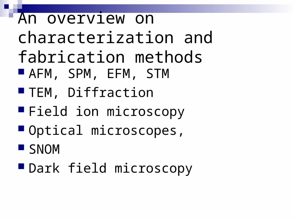
An overview on characterization and fabrication methods AFM, SPM, EFM, STM TEM, Diffraction Field ion microscopy Optical microscopes, SNOM Dark field microscopy

Fabrication in Nano-scale
Layer deposition Lithography, electron, ion Mask, resolution improvement Nano-imprint Various CMOS steps
Characterization techniques
Optical microscopes, limited resolution, Electron microscopes, atomic level resolution, TEM, powerful with ability to give diffraction
patterns, STM, SPM, AFM, PFM, MFM, tip-based
technique, not electron-beam Field Ion microscopes, near field optical
microscopes, And our-own microscope idea!!!
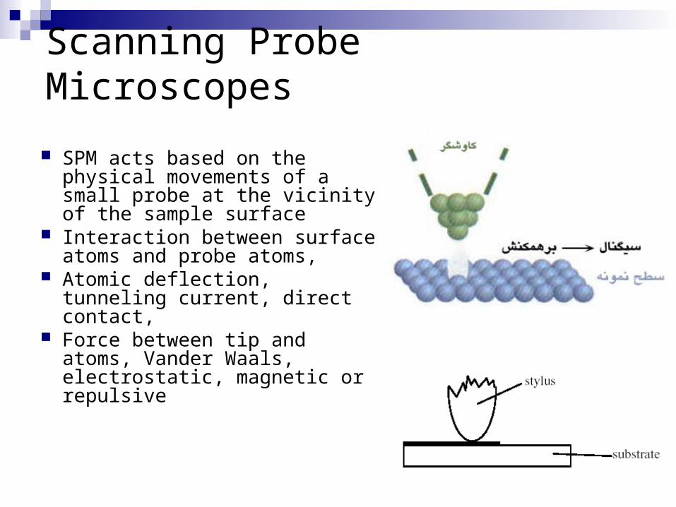
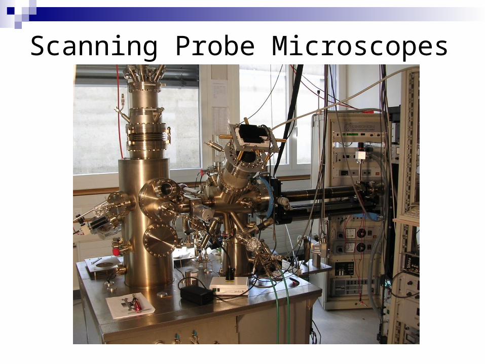
Scanning Probe Microscopes
SPM acts based on the physical movements of a small probe at the vicinity of the sample surface
Interaction between surface atoms and probe atoms,
Atomic deflection, tunneling current, direct contact,
Force between tip and atoms, Vander Waals, electrostatic, magnetic or repulsive
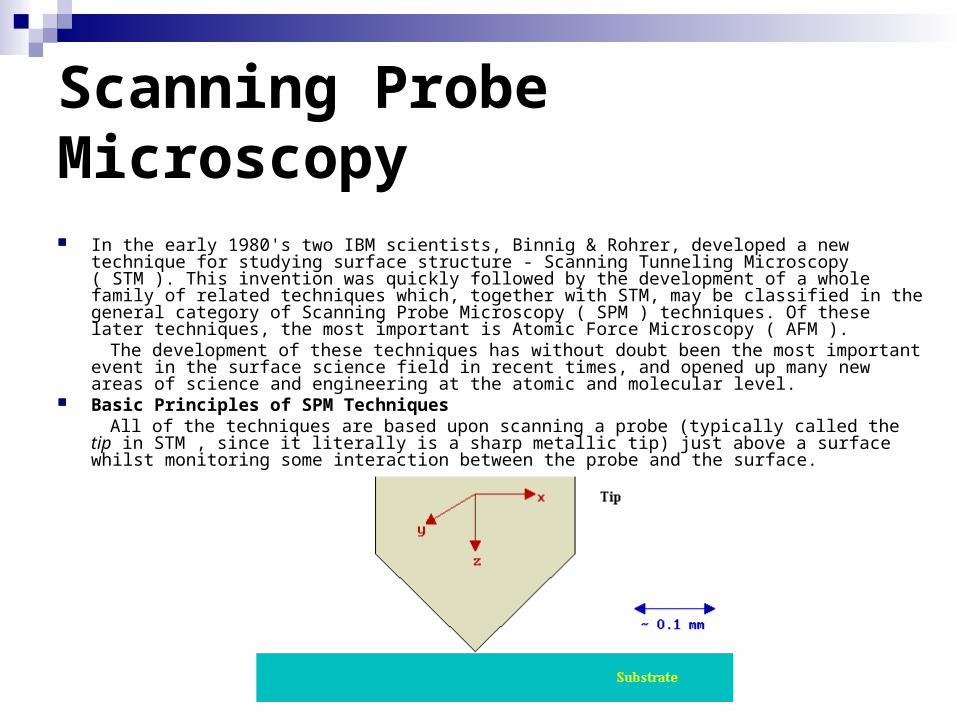
Scanning Probe Microscopy
In the early 1980's two IBM scientists, Binnig & Rohrer, developed a new technique for studying surface structure - Scanning Tunneling Microscopy ( STM ). This invention was quickly followed by the development of a whole family of related techniques which, together with STM, may be classified in the general category of Scanning Probe Microscopy ( SPM ) techniques. Of these later techniques, the most important is Atomic Force Microscopy ( AFM ).
The development of these techniques has without doubt been the most important event in the surface science field in recent times, and opened up many new areas of science and engineering at the atomic and molecular level.
Basic Principles of SPM Techniques All of the techniques are based upon scanning a probe (typically called the tip in STM , since it
literally is a sharp metallic tip) just above a surface whilst monitoring some interaction between the probe and the surface.
Scanning Probe Microscopy
The interaction that is monitored in : STM - is the tunneling current between a metallic tip and a
conducting substrate which are in very close proximity but not actually in physical contact.
AFM - is the van der Waals force between the tip and the surface; this may be either the short range repulsive force (in contact-mode) or the longer range attractive force (in non-contact mode).
For the techniques to provide information on the surface structure at the atomic level (which is what they are capable of doing ! ) :
1. the position of the tip with respect to the surface must be very accurately controlled (to within about 0.1 Å) by moving either the surface or the tip.
2. the tip must be very sharp - ideally terminating in just a single atom at its closest point of approach to the surface.
Scanning Probe Microscopy
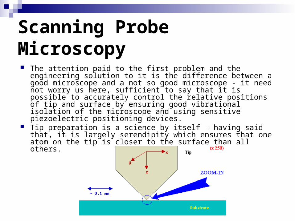
The attention paid to the first problem and the engineering solution to it is the difference between a good microscope and a not so good microscope - it need not worry us here, sufficient to say that it is possible to accurately control the relative positions of tip and surface by ensuring good vibrational isolation of the microscope and using sensitive piezoelectric positioning devices.
Tip preparation is a science by itself - having said that, it is largely serendipity which ensures that one atom on the tip is closer to the surface than all others.
Scanning Probe Microscopy
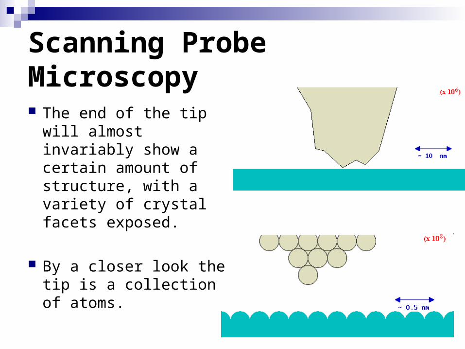
The end of the tip will almost invariably show a certain amount of structure, with a variety of crystal facets exposed.
By a closer look the tip is a collection of atoms.
Scanning Tunneling Microscopy
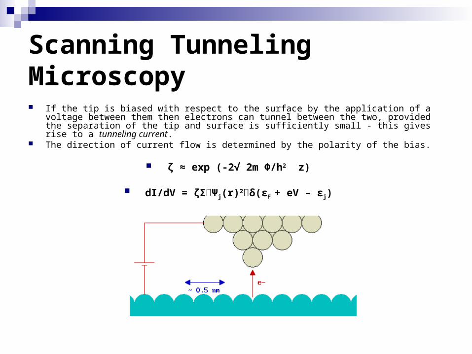
If the tip is biased with respect to the surface by the application of a voltage between them then electrons can tunnel between the two, provided the separation of the tip and surface is sufficiently small - this gives rise to a tunneling current.
The direction of current flow is determined by the polarity of the bias.
ζ ≈ exp (-2√ 2m Φ/h2 z)
dI/dV = ζΣ׀Ψj(r) 2׀ δ(εF + eV – εj)
Scanning Tunneling Microscopy
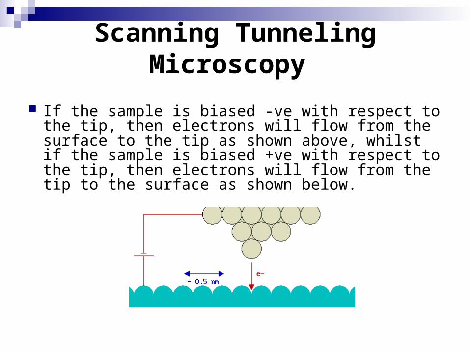
If the sample is biased -ve with respect to the tip, then electrons will flow from the surface to the tip as shown above, whilst if the sample is biased +ve with respect to the tip, then electrons will flow from the tip to the surface as shown below.
Scanning Probe Microscopes
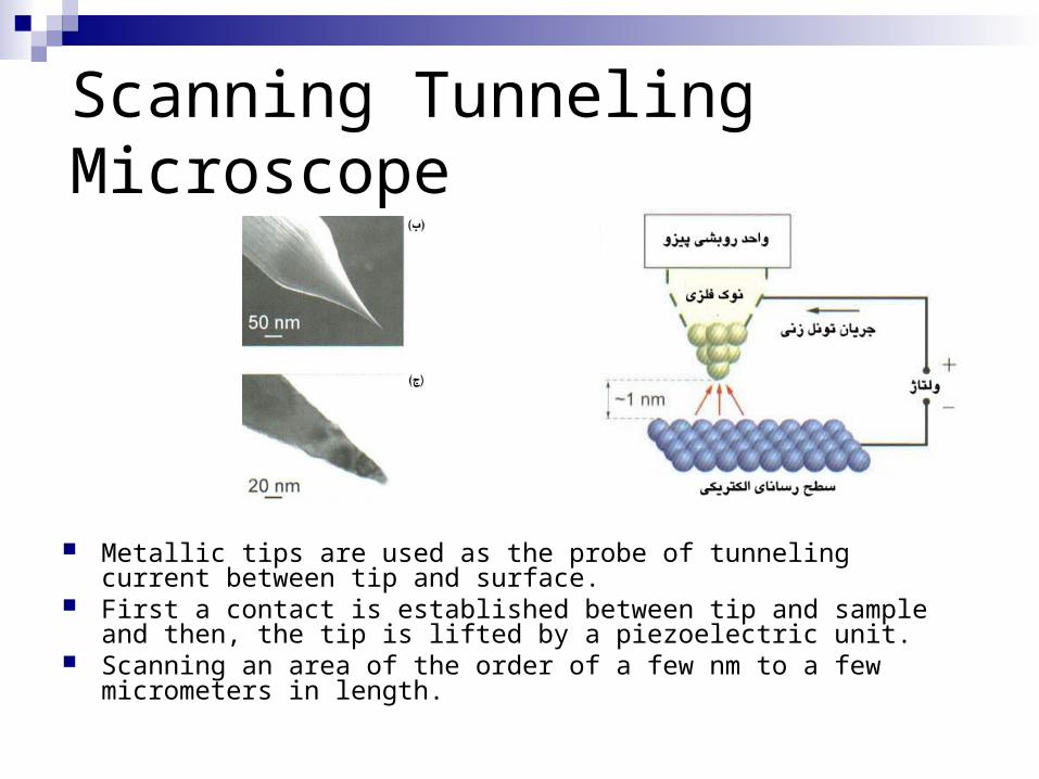
Scanning Tunneling Microscope
Metallic tips are used as the probe of tunneling current between tip and surface.
First a contact is established between tip and sample and then, the tip is lifted by a piezoelectric unit.
Scanning an area of the order of a few nm to a few micrometers in length.
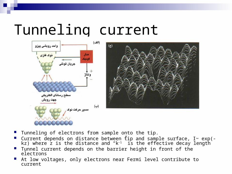
Tunneling current
Tunneling of electrons from sample onto the tip. Current depends on distance between tip and sample surface, I~ exp(-kz)
where z is the distance and “k-1” is the effective decay length Tunnel current depends on the barrier height in front of the electrons At low voltages, only electrons near Fermi level contribute to current
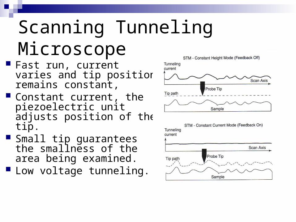
Scanning Tunneling Microscope Fast run, current varies
and tip position remains constant,
Constant current, the piezoelectric unit adjusts position of the tip.
Small tip guarantees the smallness of the area being examined.
Low voltage tunneling.
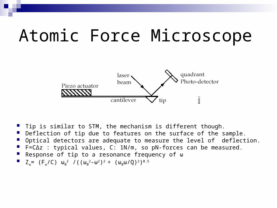
Atomic Force Microscope
Tip is similar to STM, the mechanism is different though. Deflection of tip due to features on the surface of the sample. Optical detectors are adequate to measure the level of deflection. F=CΔz : typical values, C: 1N/m, so pN-forces can be measured. Response of tip to a resonance frequency of ω Zω= (Fω/C) ω0
2 /((ω02-ω2)2 + (ω0ω/Q)2)0.5
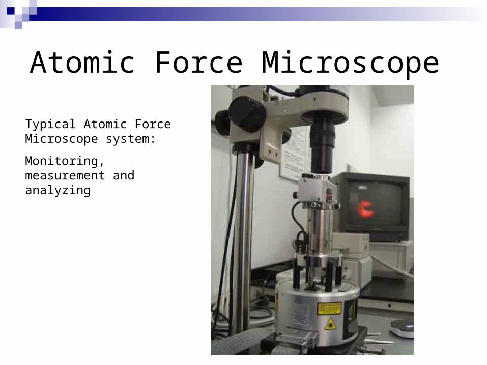
Atomic Force Microscope
Typical Atomic Force Microscope system:
Monitoring, measurement and analyzing
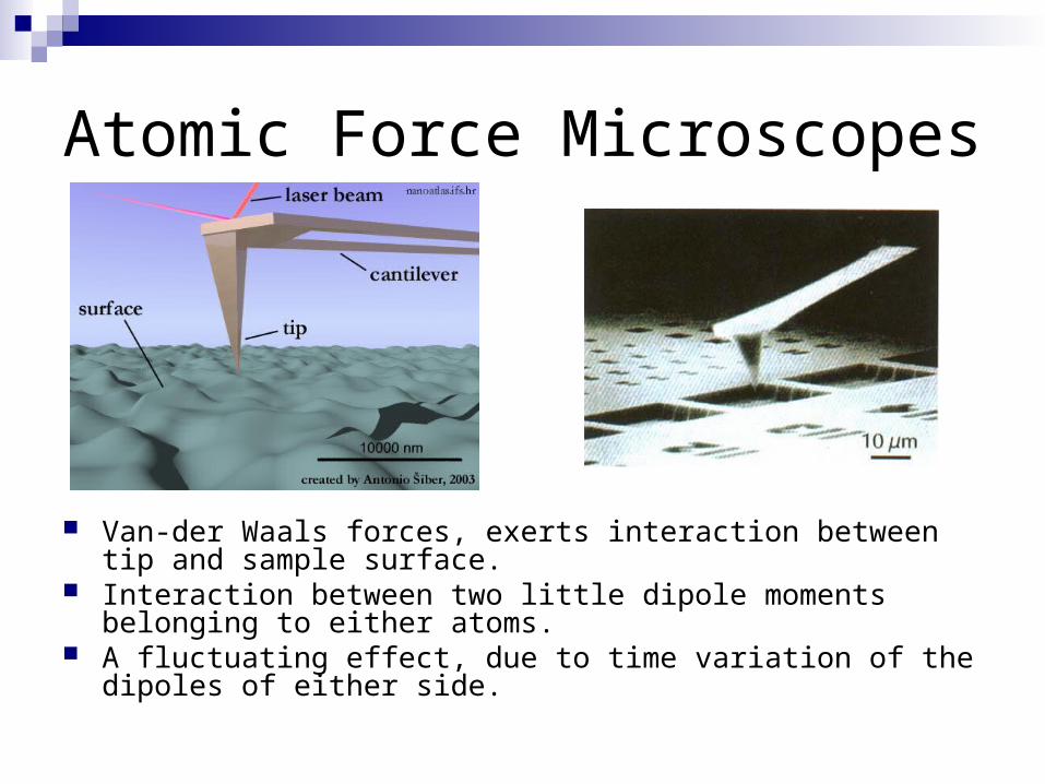
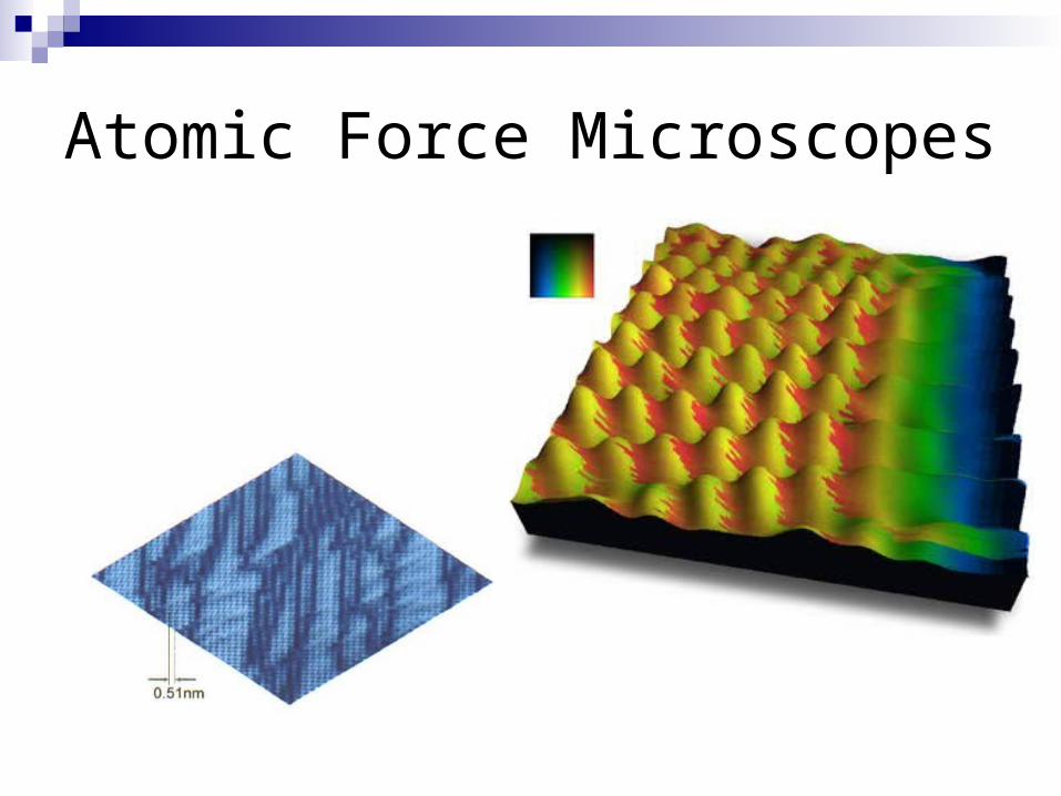
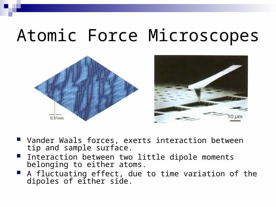
Atomic Force Microscopes
Van-der Waals forces, exerts interaction between tip and sample surface.
Interaction between two little dipole moments belonging to either atoms.
A fluctuating effect, due to time variation of the dipoles of either side.
Atomic Force Microscopes
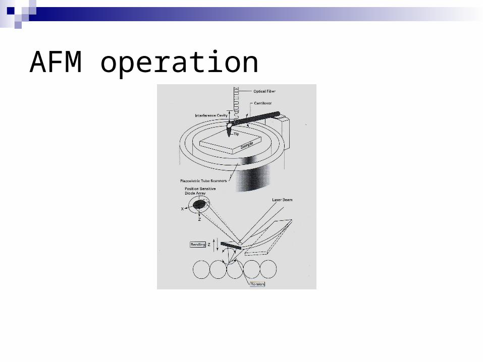
AFM operation
Atomic Force Microscopes
Vander Waals forces, exerts interaction between tip and sample surface.
Interaction between two little dipole moments belonging to either atoms.
A fluctuating effect, due to time variation of the dipoles of either side.
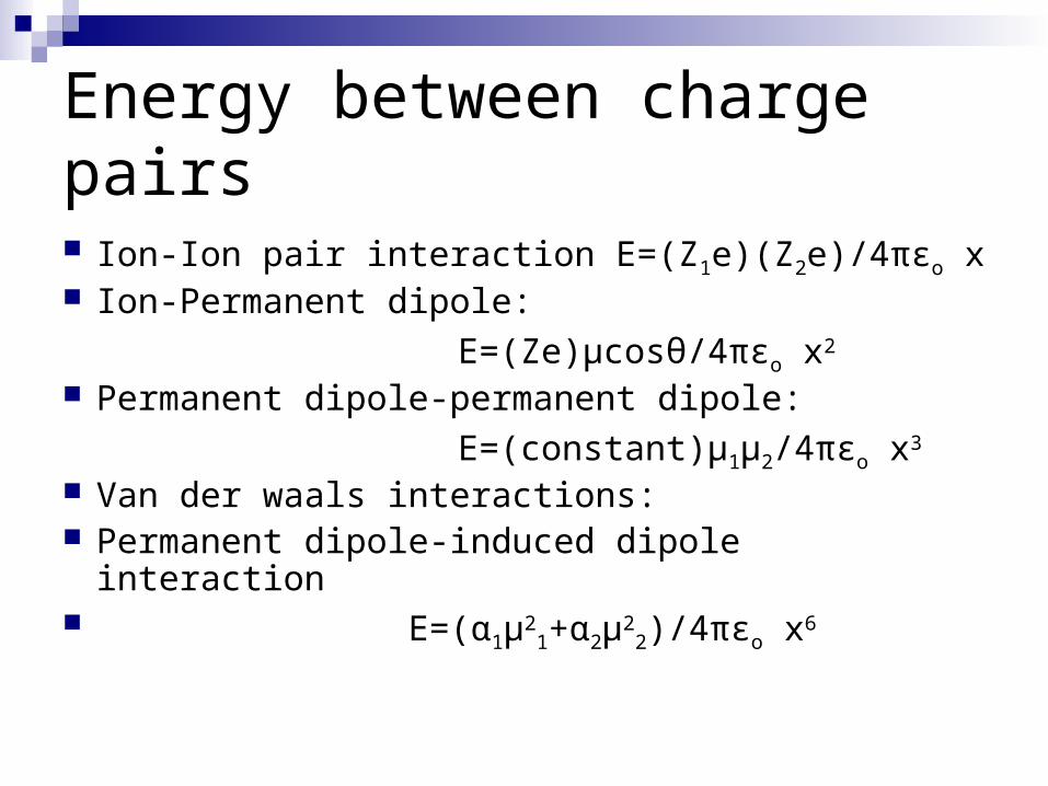
Energy between charge pairs
Ion-Ion pair interaction E=(Z1e)(Z2e)/4πεo x Ion-Permanent dipole:
E=(Ze)µcosθ/4πεo x2
Permanent dipole-permanent dipole:
E=(constant)µ1µ2/4πεo x3
Van der waals interactions: Permanent dipole-induced dipole interaction E=(α1µ2
1+α2µ22)/4πεo x6
Interactions
Short range, strong interaction: At very close separation, a strong repulsive force develops with a “x12” power. E=ζ x-12
Total interaction potential, E=ζ x-12 – βx-6
Attractions between spherical particles is assumed to be the summation of all individual atoms or molecules.
dE=-0.5 ρ2β/x6 dV1 dV2 (ρ: number of atoms in unit volume)
Two identical spheres, (R>> x) E=-AR/12x Different radii, R1 and R2 E=-AR1R2 /6x(R1 + R2) Two surfaces, E=-A/(12 πx2) In all cases, A= ρ2 π2 β which is called “Hamker constant”
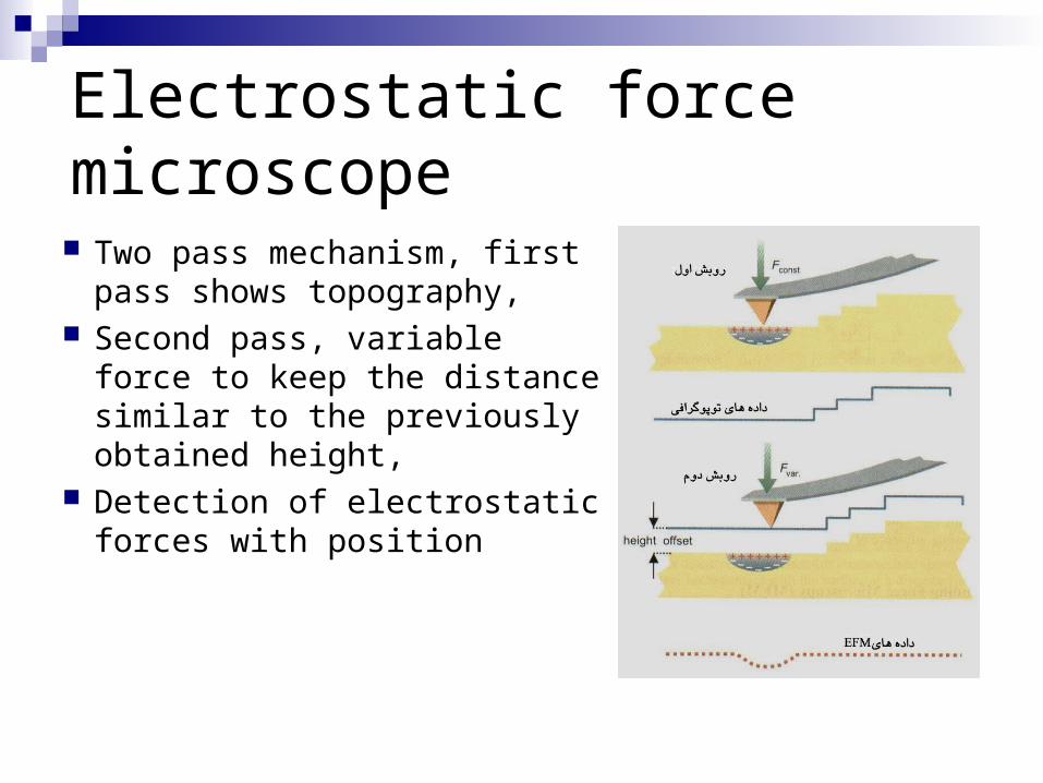
Electrostatic force microscope
Two pass mechanism, first pass shows topography,
Second pass, variable force to keep the distance similar to the previously obtained height,
Detection of electrostatic forces with position
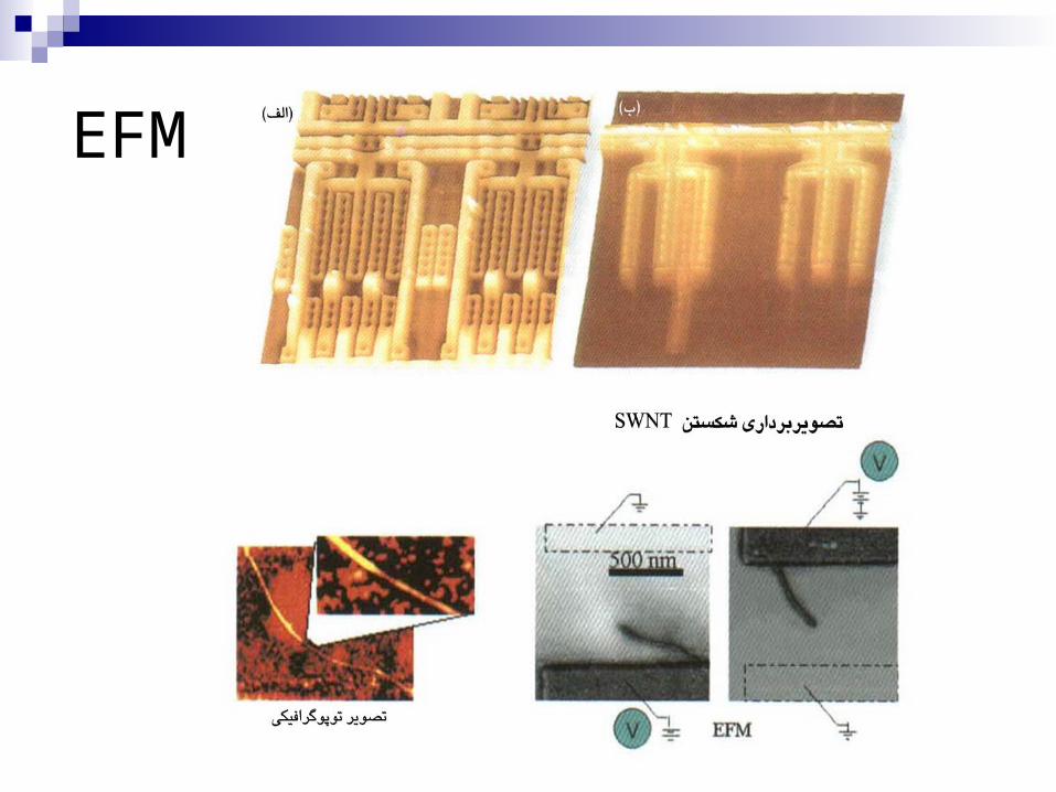
EFM
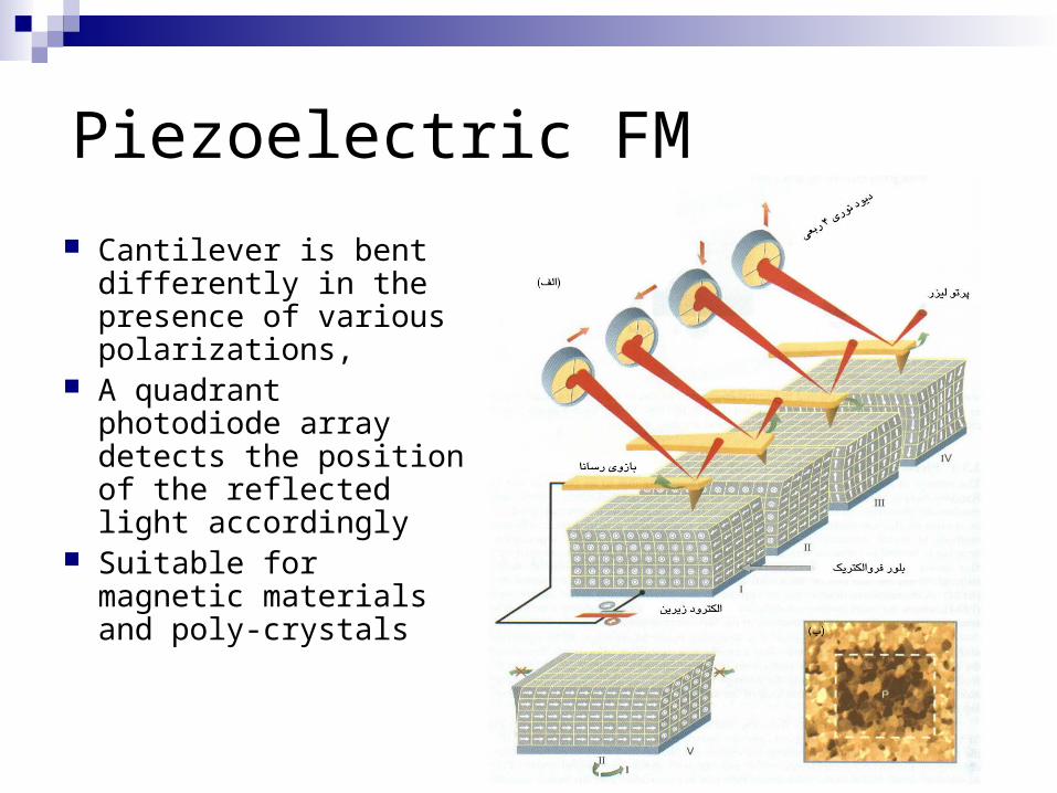
Piezoelectric FM
Cantilever is bent differently in the presence of various polarizations,
A quadrant photodiode array detects the position of the reflected light accordingly
Suitable for magnetic materials and poly-crystals
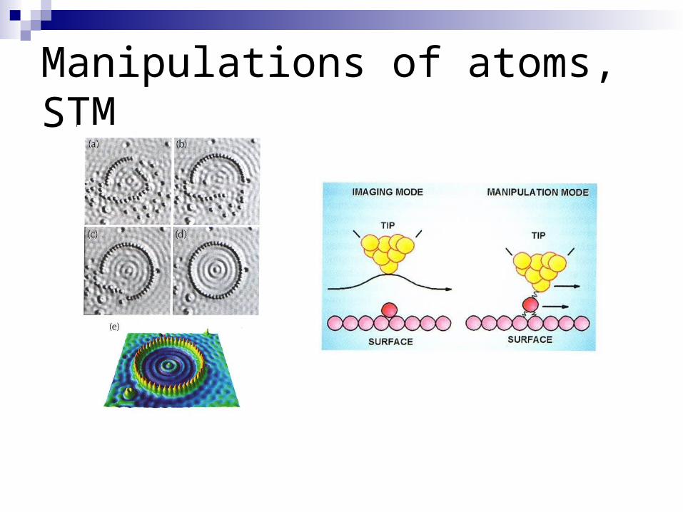
Manipulations of atoms, STM
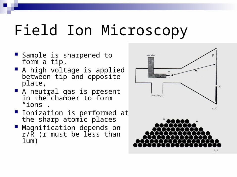
Field Ion Microscopy
Sample is sharpened to form a tip,
A high voltage is applied between tip and opposite plate,
A neutral gas is present in the chamber to form “ions”.
Ionization is performed at the sharp atomic places
Magnification depends on r/R (r must be less than 1um)
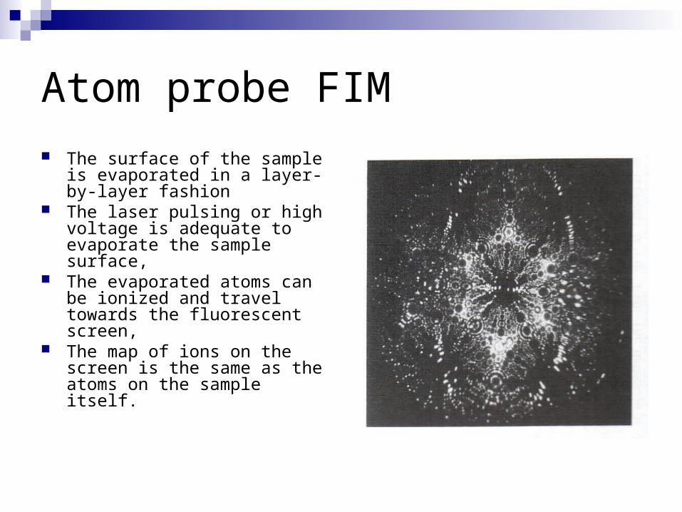
Atom probe FIM
The surface of the sample is evaporated in a layer-by-layer fashion
The laser pulsing or high voltage is adequate to evaporate the sample surface,
The evaporated atoms can be ionized and travel towards the fluorescent screen,
The map of ions on the screen is the same as the atoms on the sample itself.
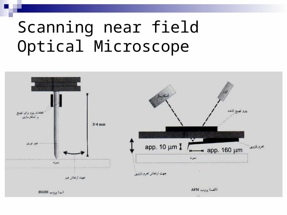
Scanning near field Optical Microscope
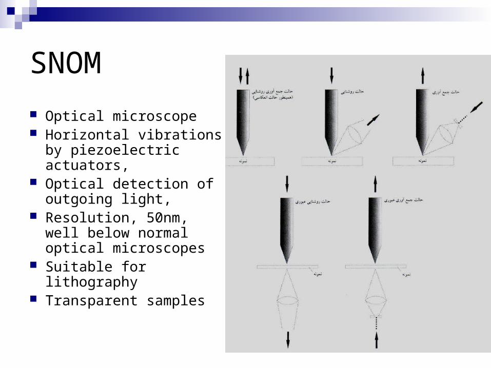
SNOM
Optical microscope Horizontal vibrations by
piezoelectric actuators, Optical detection of
outgoing light, Resolution, 50nm, well
below normal optical microscopes
Suitable for lithography Transparent samples
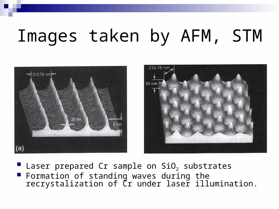
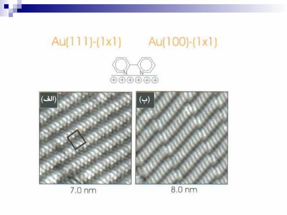
Images taken by AFM, STM
Laser prepared Cr sample on SiO2 substrates Formation of standing waves during the recrystalization
of Cr under laser illumination.
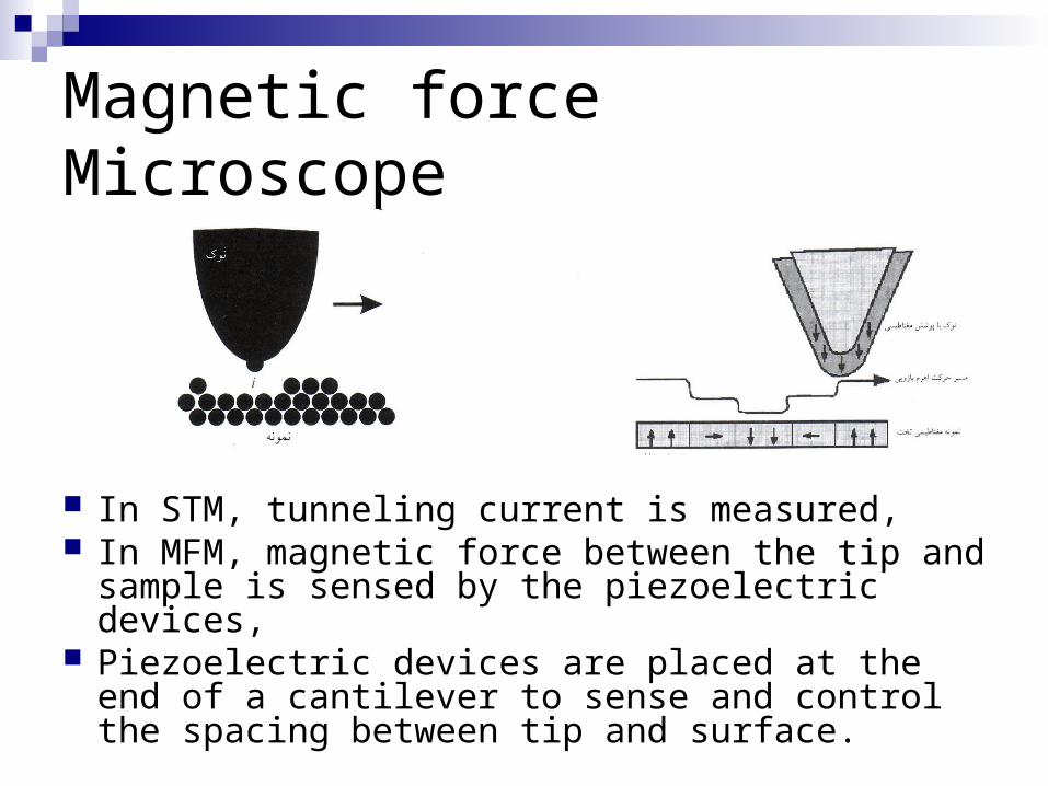
Magnetic force Microscope
In STM, tunneling current is measured, In MFM, magnetic force between the tip and
sample is sensed by the piezoelectric devices, Piezoelectric devices are placed at the end of a
cantilever to sense and control the spacing between tip and surface.
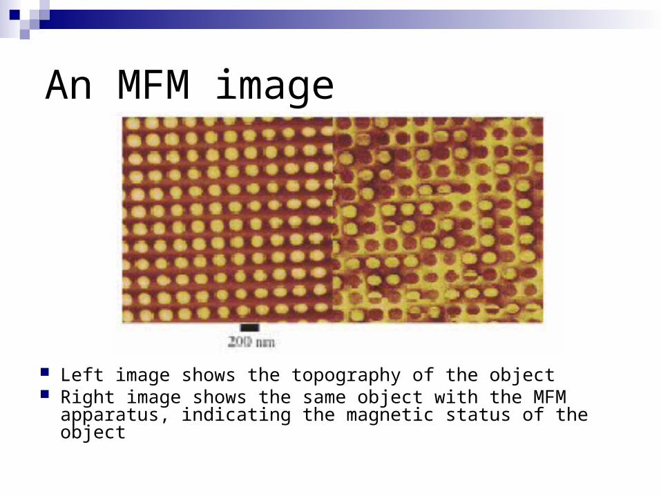
An MFM image
Left image shows the topography of the object Right image shows the same object with the MFM
apparatus, indicating the magnetic status of the object