Embed Size (px)
Citation preview
0885-8993 (c) 2013 IEEE. Personal use is permitted, but republication/redistribution requires IEEE permission. Seehttp://www.ieee.org/publications_standards/publications/rights/index.html for more information.
This article has been accepted for publication in a future issue of this journal, but has not been fully edited. Content may change prior to final publication. Citation information: DOI10.1109/TPEL.2014.2315834, IEEE Transactions on Power Electronics
1
Abstract—The proposed converter has the following features: 1) zero current commutation (ZCC) and natural voltage clamping (NVC) eliminate the need for active-clamp circuits or passive snubbers required to absorb surge voltage in conventional current-fed topologies; 2) Switching losses are reduced significantly owing to zero-current switching (ZCS) of primary side devices and zero-voltage switching (ZVS) of secondary side devices. Turn-on switching transition loss of primary devices is also negligible. 3) Soft-switching and NVC are inherent and load independent. 4) The voltage across primary side device is independent of duty cycle with varying input voltage and output power and clamped at rather low reflected output voltage enabling the use of low voltage semiconductor devices. These merits make the converter good candidate for interfacing low voltage dc bus with high voltage dc bus for higher current applications. Steady state, analysis, design, simulation and experimental results are presented.
Index Terms—Current-fed converter, DC/DC converter,
Natural clamping, Soft-switching, Zero-current commutation.
I INTRODUCTION
RANSPORTATION electrification has received significant interest owing to limited supply of fossil fuels
and concern of global climate change [1-2]. Battery based Electric vehicles (EVs) and Fuel Cell Vehicles (FCVs) are emerging as viable solutions for transportation electrification with lower emission, better vehicle performance and higher fuel economy. Compared with pure battery based EVs, FCVs are quite appealing with the merits of zero-emission, satisfied driving range, short refueling time, high efficiency, and high reliability. A diagram of a typical FCV propulsion system is shown in Fig. 1 [3-5]. Bidirectional and unidirectional dc/dc converters are utilized to develop high voltage bus for the inverter. The energy storage system (ESS) is used to overcome the limitations of lacking energy storage capability and fast power transient of FCVs.
Bidirectional converter with high boost ratio and high efficiency is required to connect the low-voltage ESS and high voltage dc link bus. Compared with non-isolated topologies, high frequency (HF) transformer isolated converters are preferred with merits of high step up ratio, galvanic isolation and flexibility of system configuration [6]. HF transformer isolated converters could be either voltage-fed [7-9] or current-fed [10-20]. Advantages and disadvantages of both types are compared in [21-23]. The voltage-fed converters have
Fig. 1. Diagram of a FCV propulsion system.
low switch voltage ratings enabling the use of switches with low on-state resistance. This can significantly reduce conduction loss of primary side switches. However, voltage-fed converters suffer from several limitations, i.e. high pulsating current at input, limited soft-switching range, rectifier diode ringing, duty cycle loss (if inductive output filter), high circulating current through devices and magnetics, and relatively low efficiency for high voltage amplification and high input current applications. Compared with voltage-fed converters, current-fed converters exhibit smaller input current ripple, lower diode voltage rating, lower transformer turns-ratio, negligible diode ringing, no duty cycle loss, and easier current control ability. Besides, current-fed converters can precisely control the charging and discharging current of ESS, which helps achieving higher charging/discharging efficiency. Thus current-fed converter is more feasible for the application of ESS in FCVs.
Three topologies of isolated current-fed dc/dc converters, i.e. full-bridge [10-12], L-type half bridge [13-15], and push-pull [16-17] have been researched. One drawback of current-fed converters is the high turn-off voltage spike across the devices. Normally, active-clamp circuits [14-16, 24-25], RCD passive snubbers [11] or energy recovery snubber [6] are employed to absorb the surge voltage and assist soft-switching. In RCD snubbers, energy absorbed by the clamping capacitor is dissipated in the resistor resulting in low efficiency. Active-clamp suffers from high current stress (peak) and higher circulating current at light load.
The leakage inductance and parasitic capacitance of the HF transformer were utilized to achieve zero current switching (ZCS) in [17-19]. However, resonant current is much higher than input current that increases the current stress of devices and magnetics requiring higher VA rating components. Besides, the variable frequency modulation makes the control implementation difficult and complex [20]. External auxiliary circuits are utilized to achieve ZCS and reduce the circulating current in [26-28] but complex. Although the trapped energy
Naturally Clamped Zero Current Commutated Soft-switching Current-fed Push-Pull DC/DC
Converter: Analysis, Design, and Experimental ResultsPan Xuewei, Student Member, IEEE and Akshay K Rathore, Senior Member, IEEE
T
0885-8993 (c) 2013 IEEE. Personal use is permitted, but republication/redistribution requires IEEE permission. Seehttp://www.ieee.org/publications_standards/publications/rights/index.html for more information.
This article has been accepted for publication in a future issue of this journal, but has not been fully edited. Content may change prior to final publication. Citation information: DOI10.1109/TPEL.2014.2315834, IEEE Transactions on Power Electronics
2
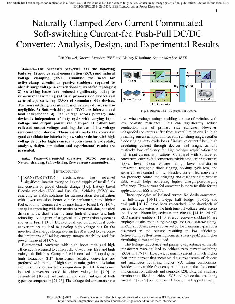
Fig.2. Proposed ZCS current-fed push-pull dc/dc converter.
can be recycled, the auxiliary circuits still contribute to a significant amount of loss. In current-fed bidirectional converter, active soft commutation technique [11, 29-30] is proposed to divert the switch current to another switch through transformer to achieve natural or zero current commutation thus reducing or eliminating the need of snubber.
In this paper, a novel secondary modulation based naturally clamped soft-switching bidirectional snubberless current-fed push-pull converter is proposed as shown in Fig. 2. Natural voltage clamping (NVC) with ZCS of primary devices is achieved by proposed secondary modulation and therefore avoids the need of passive snubbers or active-clamp making it snubberless. Switching losses are reduced significantly owing to ZCS of primary switches and ZVS of secondary switches that permits HF switching operation with smaller magnetics.
The objectives of this paper are to explain steady-state operation and analysis, illustrate design, and demonstrate experimental performance of the proposed converter. The objectives are realized and outlined in various Sections as follows: Steady-state operation of the converter is explained and its mathematical analysis is reported in Section II. Detailed converter design procedure is illustrated in Section III. Analysis and design are verified by simulation results using PSIM 9.0.4 in Section IV. Experimental results on a laboratory prototype of 250W are demonstrated to validate and show the converter performance in Section IV.
II OPERATION AND ANALYSIS OF THE CONVERTER
For the sake of simplicity, the following assumptions are made to study the operation and explain the analysis of the converter: a) Boost inductor L is large enough to maintain constant current through it. b) All the components are ideal. c) Series inductors Llk1 and Llk2 include the leakage inductances of the transformer. The total value of Llk1 and Llk2 is represented as Llk_T. Llk represents the equivalent series inductor reflected to the high voltage side. d) Magnetizing inductance of the transformer is infinitely large.
A. Boost mode (Discharging Mode) Operation
In this part, steady-state operation and analysis with zero current commutation (ZCC) and NVC concept has been explained. Before turning off one of primary side switches (say S1), the other switch (say S2) is turned-on. Reflected output voltage 2Vo/n appears across the transformer primary. It diverts the current from one switch to the other one through transformer causing current through just triggered switch to rise and the current through conducting switch to fall to zero naturally resulting in ZCC. Later the body diode across switch start conducting and its gating signal is removed leading to ZCS
turn-off of the device. Commutated device capacitance starts charging with NVC.
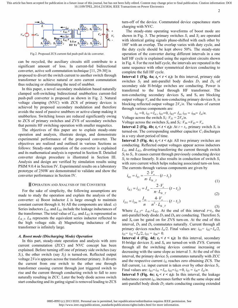
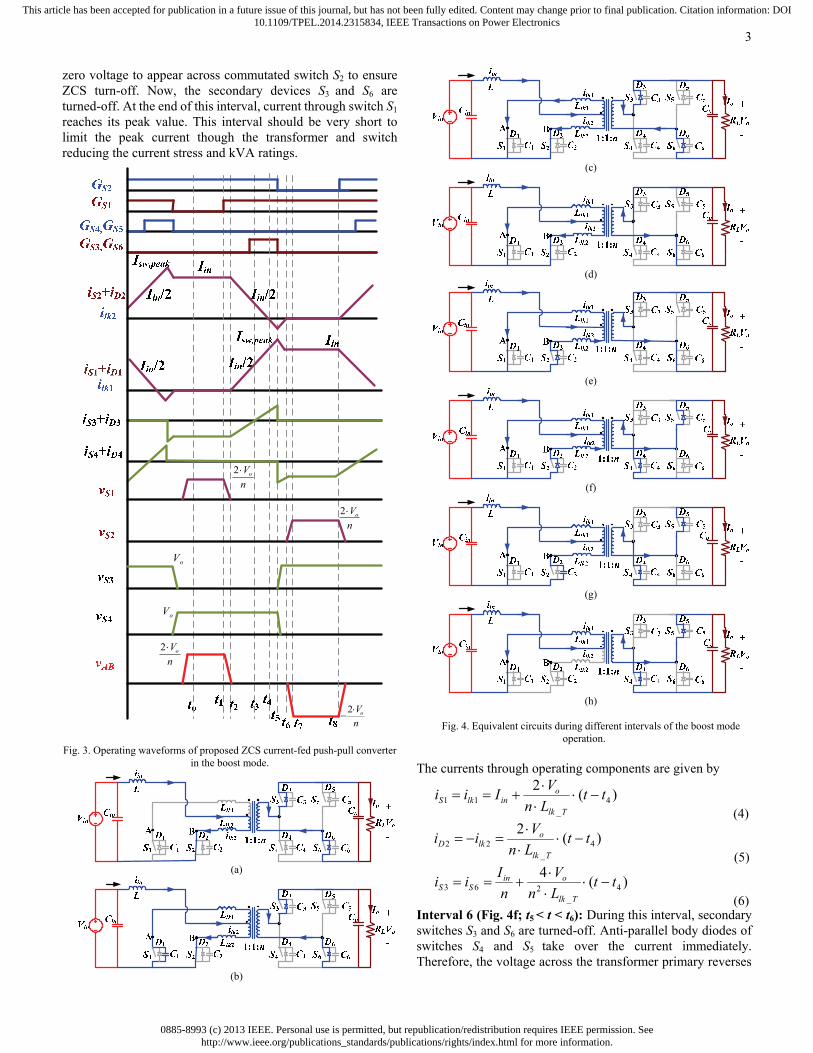
The steady-state operating waveforms of boost mode are shown in Fig. 3. The primary switches S1 and S2 are operated with identical gating signals phase-shifted with each other by 180o with an overlap. The overlap varies with duty cycle, and the duty cycle should be kept above 50%. The steady-state operation of the converter during different intervals in a one half HF cycle is explained using the equivalent circuits shown in Fig. 4. For the rest half cycle, the intervals are repeated in the same sequence with other symmetrical devices conducting to complete the full HF cycle. Interval 1 (Fig. 4a; to < t < t1): In this interval, primary side switches S2 and anti-parallel body diodes D3 and D6 of secondary side H-bridge switches are conducting. Power is transferred to the load through HF transformer. The non-conducting secondary devices S4 and S5 are blocking output voltage Vo and the non-conducting primary devices S1 is blocking reflected output voltage 2Vo/n. The values of current through various components are: iS1 =0, iS2 =Iin , ilk1=0, ilk2= Iin, iD3 = iD6= Iin/n. Voltage across the switch S1: VS1 = 2Vo/n. Voltage across the switches S4 and S5: VS4 =VS5 = Vo. Interval 2 (Fig. 4b; t1 < t < t2): At t = t1, primary switch S1 is turned-on. The corresponding snubber capacitor C1 discharges in a very short period of time. Interval 3 (Fig. 4c; t2 < t < t3): All two primary switches are conducting. Reflected output voltages appear across inductors Llk1 and Llk2, diverting/transferring the current through switch S2 to S1. It causes current through previously conducting device S2 to reduce linearly. It also results in conduction of switch S1 with zero current which helps reducing associated turn-on loss. The currents through various components are given by
)(2
2_
11 ttLn
Vii
Tlk
oSlk
(1)
)(2
2_
22 ttLn
VIii
Tlk
oinSlk
(2)
)(4
2_
263 ttLn
V
n
Iii
Tlk
oinDD
(3)
Where Llk_T= Llk1+Llk2. At the end of this interval t=t3, the anti-parallel body diode D3 and D6 are conducting. Therefore S3 and S6 can be gated on for ZVS turn-on. At the end of this interval, D3 and D6 commutates naturally. Current through all primary devices reaches Iin/2. Final values are: ilk1= ilk2=Iin/2, iS1= iS2 =Iin/2, iD3 = iD6= 0. Interval 4 (Fig. 4d; t3 < t < t4): In this interval, secondary H-bridge devices S3 and S6 are turned-on with ZVS. Currents through all the switching devices continue increasing or decreasing with the same slope as interval 3. At the end of this interval, the primary device S2 commutates naturally with ZCC and the respective current iS2 reaches zero obtaining ZCS. The full current, i.e. input current is taken over by other device S1. Final values are: ilk1=iS1 =Iin, ilk2=iS2 =0, iS3 = iS6= Iin/n. Interval 5 (Fig. 4e; t4 < t < t5): In this interval, the leakage inductance current ilk1 increases further with the same slope and anti-parallel body diode D2 starts conducting causing extended
0885-8993 (c) 2013 IEEE. Personal use is permitted, but republication/redistribution requires IEEE permission. Seehttp://www.ieee.org/publications_standards/publications/rights/index.html for more information.
This article has been accepted for publication in a future issue of this journal, but has not been fully edited. Content may change prior to final publication. Citation information: DOI10.1109/TPEL.2014.2315834, IEEE Transactions on Power Electronics
3
zero voltage to appear across commutated switch S2 to ensure ZCS turn-off. Now, the secondary devices S3 and S6 are turned-off. At the end of this interval, current through switch S1 reaches its peak value. This interval should be very short to limit the peak current though the transformer and switch reducing the current stress and kVA ratings.
oV
oV
n
Vo2
n
Vo2
n
Vo2
n
Vo
2
Fig. 3. Operating waveforms of proposed ZCS current-fed push-pull converter
in the boost mode.
(a)
(b)
(c)
(d)
(e)
(f)
(g)
(h)
Fig. 4. Equivalent circuits during different intervals of the boost mode
operation.
The currents through operating components are given by
)(2
4_
11 ttLn
VIii
Tlk
oinlkS
(4)
)(2
4_
22 ttLn
Vii
Tlk
olkD
(5)
)(4
4_
263 ttLn
V
n
Iii
Tlk
oinSS
(6)
Interval 6 (Fig. 4f; t5 < t < t6): During this interval, secondary switches S3 and S6 are turned-off. Anti-parallel body diodes of switches S4 and S5 take over the current immediately. Therefore, the voltage across the transformer primary reverses
0885-8993 (c) 2013 IEEE. Personal use is permitted, but republication/redistribution requires IEEE permission. Seehttp://www.ieee.org/publications_standards/publications/rights/index.html for more information.
This article has been accepted for publication in a future issue of this journal, but has not been fully edited. Content may change prior to final publication. Citation information: DOI10.1109/TPEL.2014.2315834, IEEE Transactions on Power Electronics
4
polarity. The current through the switch S1 and body diodes D2 also start decreasing.
The currents through operating components are given by
)(2
5_
,11 ttLn
VIii
Tlk
opeakswlkS
(7)
)(2
5_
,222 ttLn
VIii
Tlk
opeakDlkD
(8)
)(4
5_
2
,54 tt
Ln
V
n
Iii
Tlk
opeaklkDD
(9)
At the end of this interval, current through D2 reduce to zero and is commutated naturally. Current through S1 reaches Iin. Final values: ilk1= iS1=Iin, ilk2= iD2 =0, iD4 = iD5= Iin/n. Interval 7 (Fig. 4g; t6 < t < t7): In this interval, snubber capacitor C2 charges to 2Vo/n in a short period of time. Switch S2 is in forward blocking mode now. Interval 8 (Fig. 4h; t7 < t < t8): In this interval, currents through S1 and transformer are constant at input current Iin . Current through anti-parallel body diodes of the secondary switches D4 and D5 is at Iin/n. The final values are: ilk1=iS1 =Iin, ilk2=iS2 =0, iD4 = iD5= Iin/n. Voltage across the switch S2 VS2 = 2Vo/n. In this half HF cycle, current has transferred from switch S2 to S1, and the transformer current has reversed its polarity. B. Buck mode (Charging Mode) Operation
In the reverse direction, the converter acts as a standard voltage-fed full-bridge center-tapped converter with inductive output filter. The regenerative braking energy can be fed back and recharge the low voltage storage from high voltage bus, thus increasing overall system efficiency. Standard phase-shift PWM control technique is employed to achieve ZVS of high voltage side and ZCS of low voltage side. At low voltage side, devices need not be controlled because body diodes of the devices can take over as high-frequency rectifier.
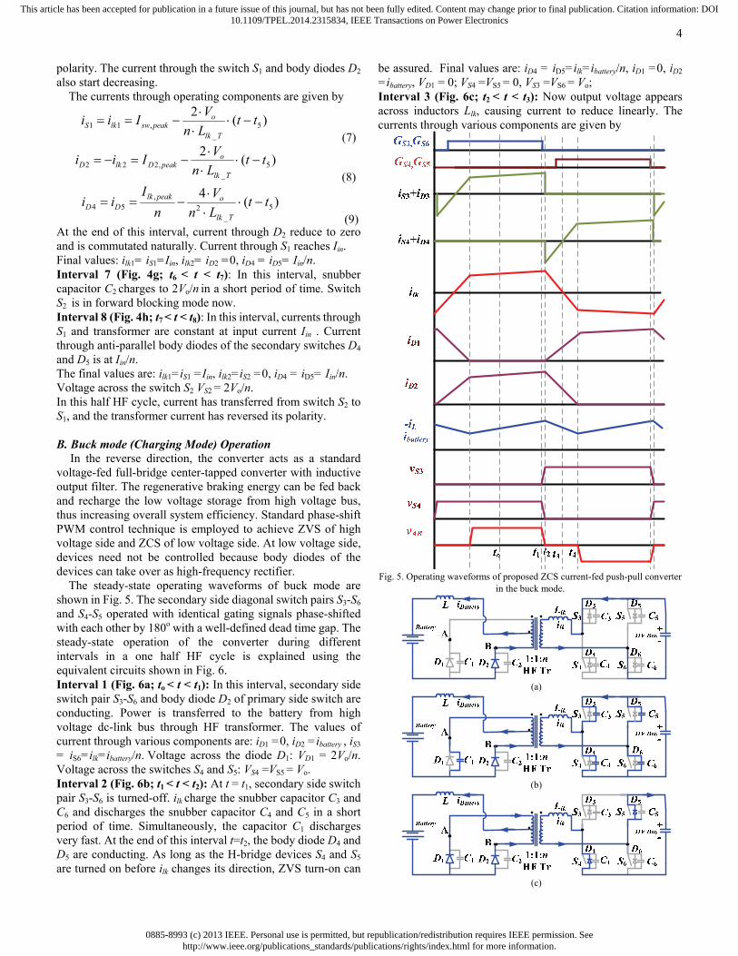
The steady-state operating waveforms of buck mode are shown in Fig. 5. The secondary side diagonal switch pairs S3-S6 and S4-S5 operated with identical gating signals phase-shifted with each other by 180o with a well-defined dead time gap. The steady-state operation of the converter during different intervals in a one half HF cycle is explained using the equivalent circuits shown in Fig. 6. Interval 1 (Fig. 6a; to < t < t1): In this interval, secondary side switch pair S3-S6 and body diode D2 of primary side switch are conducting. Power is transferred to the battery from high voltage dc-link bus through HF transformer. The values of current through various components are: iD1 =0, iD2 =ibattery , iS3 = iS6=ilk=ibattery/n. Voltage across the diode D1: VD1 = 2Vo/n. Voltage across the switches S4 and S5: VS4 =VS5 = Vo. Interval 2 (Fig. 6b; t1 < t < t2): At t = t1, secondary side switch pair S3-S6 is turned-off. ilk charge the snubber capacitor C3 and C6 and discharges the snubber capacitor C4 and C5 in a short period of time. Simultaneously, the capacitor C1 discharges very fast. At the end of this interval t=t2, the body diode D4 and D5 are conducting. As long as the H-bridge devices S4 and S5 are turned on before ilk changes its direction, ZVS turn-on can
be assured. Final values are: iD4 = iD5=ilk=ibattery/n, iD1 =0, iD2 =ibattery, VD1 = 0; VS4 =VS5 = 0, VS3 =VS6 = Vo; Interval 3 (Fig. 6c; t2 < t < t3): Now output voltage appears across inductors Llk, causing current to reduce linearly. The currents through various components are given by
Fig. 5. Operating waveforms of proposed ZCS current-fed push-pull converter
in the buck mode.
(a)
(b)
(c)
0885-8993 (c) 2013 IEEE. Personal use is permitted, but republication/redistribution requires IEEE permission. Seehttp://www.ieee.org/publications_standards/publications/rights/index.html for more information.
This article has been accepted for publication in a future issue of this journal, but has not been fully edited. Content may change prior to final publication. Citation information: DOI10.1109/TPEL.2014.2315834, IEEE Transactions on Power Electronics
5
(d)
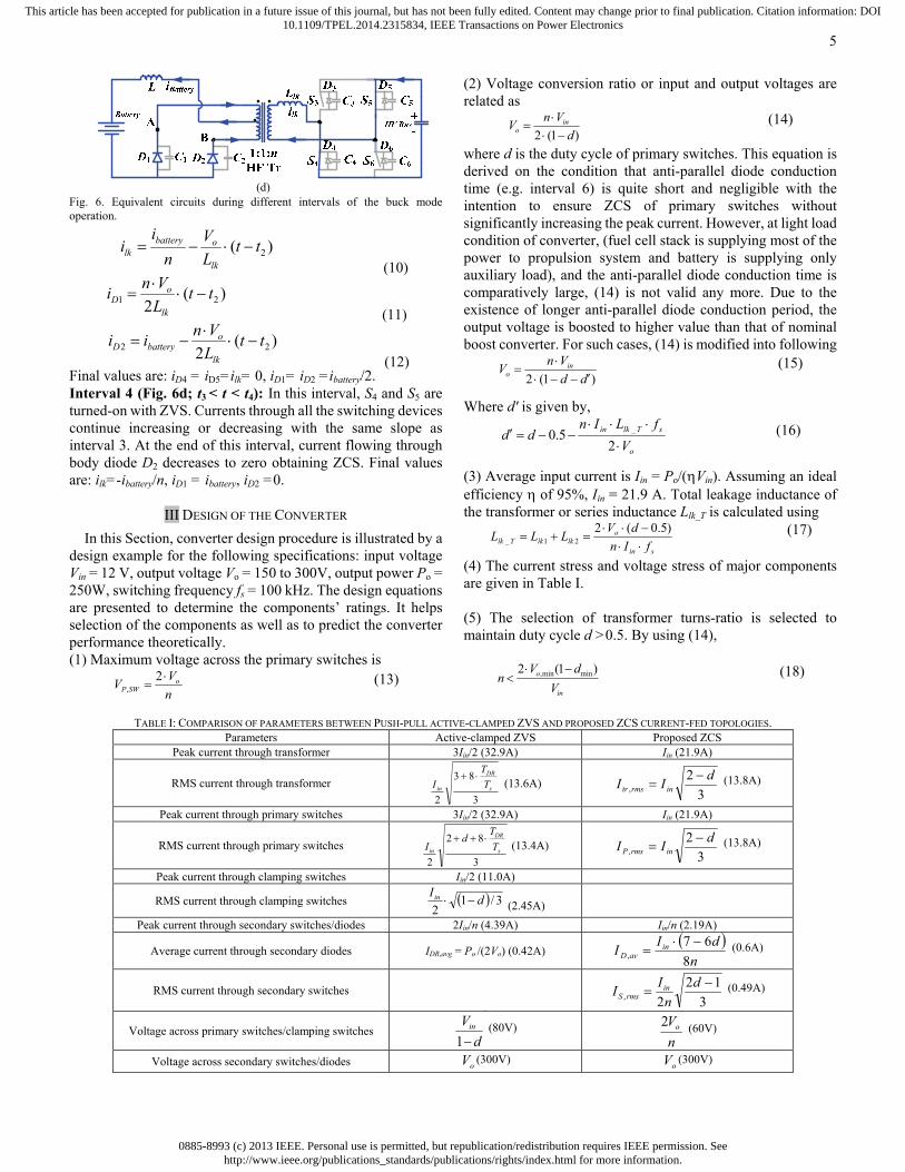
Fig. 6. Equivalent circuits during different intervals of the buck mode operation.
)( 2ttL
V
n
ii
lk
obatterylk
(10)
)(2 21 tt
L
Vni
lk
oD
(11)
)(2 22 tt
L
Vnii
lk
obatteryD
(12) Final values are: iD4 = iD5=ilk= 0, iD1= iD2 =ibattery/2. Interval 4 (Fig. 6d; t3 < t < t4): In this interval, S4 and S5 are turned-on with ZVS. Currents through all the switching devices continue increasing or decreasing with the same slope as interval 3. At the end of this interval, current flowing through body diode D2 decreases to zero obtaining ZCS. Final values are: ilk=-ibattery/n, iD1 = ibattery, iD2 =0.
III DESIGN OF THE CONVERTER
In this Section, converter design procedure is illustrated by a design example for the following specifications: input voltage Vin = 12 V, output voltage Vo = 150 to 300V, output power Po = 250W, switching frequency fs = 100 kHz. The design equations are presented to determine the components’ ratings. It helps selection of the components as well as to predict the converter performance theoretically. (1) Maximum voltage across the primary switches is
n
VV o
SWP
2,
(13)
(2) Voltage conversion ratio or input and output voltages are related as
)1(2 d
VnV in
o
(14)
where d is the duty cycle of primary switches. This equation is derived on the condition that anti-parallel diode conduction time (e.g. interval 6) is quite short and negligible with the intention to ensure ZCS of primary switches without significantly increasing the peak current. However, at light load condition of converter, (fuel cell stack is supplying most of the power to propulsion system and battery is supplying only auxiliary load), and the anti-parallel diode conduction time is comparatively large, (14) is not valid any more. Due to the existence of longer anti-parallel diode conduction period, the output voltage is boosted to higher value than that of nominal boost converter. For such cases, (14) is modified into following
)1(2 dd
VnV in
o
(15)
Where d' is given by,
o
sTlkin
V
fLIndd
25.0 _ (16)
(3) Average input current is Iin = Po/(Vin). Assuming an ideal efficiency of 95%, Iin = 21.9 A. Total leakage inductance of the transformer or series inductance Llk_T is calculated using
sin
olklkTlk fIn
dVLLL
)5.0(2
21_ (17)
(4) The current stress and voltage stress of major components are given in Table I.
(5) The selection of transformer turns-ratio is selected to maintain duty cycle d >0.5. By using (14),
in
o
V
dVn
)1(2 minmin,
(18)
TABLE I: COMPARISON OF PARAMETERS BETWEEN PUSH-PULL ACTIVE-CLAMPED ZVS AND PROPOSED ZCS CURRENT-FED TOPOLOGIES.
Parameters Active-clamped ZVS Proposed ZCS Peak current through transformer 3Iin/2 (32.9A) Iin (21.9A)
RMS current through transformer 3
83
2s
DR
in T
T
I
(13.6A) 3
2,
dII inrmstr
(13.8A)
Peak current through primary switches 3Iin/2 (32.9A) Iin (21.9A)
RMS current through primary switches 3
82
2s
DR
in T
Td
I
(13.4A) 3
2,
dII inrmsP
(13.8A)
Peak current through clamping switches Iin/2 (11.0A)
RMS current through clamping switches 3/12
dIin (2.45A)
Peak current through secondary switches/diodes 2Iin/n (4.39A) Iin/n (2.19A)
Average current through secondary diodes IDR,avg = Po /(2Vo) (0.42A)
n
dII in
avD 8
67,
(0.6A)
RMS current through secondary switches
-
3
12
2,
d
n
II in
rmsS (0.49A)
Voltage across primary switches/clamping switches d
Vin
1 (80V)
n
Vo2 (60V)
Voltage across secondary switches/diodes oV (300V) oV (300V)
0885-8993 (c) 2013 IEEE. Personal use is permitted, but republication/redistribution requires IEEE permission. Seehttp://www.ieee.org/publications_standards/publications/rights/index.html for more information.
This article has been accepted for publication in a future issue of this journal, but has not been fully edited. Content may change prior to final publication. Citation information: DOI10.1109/TPEL.2014.2315834, IEEE Transactions on Power Electronics
6
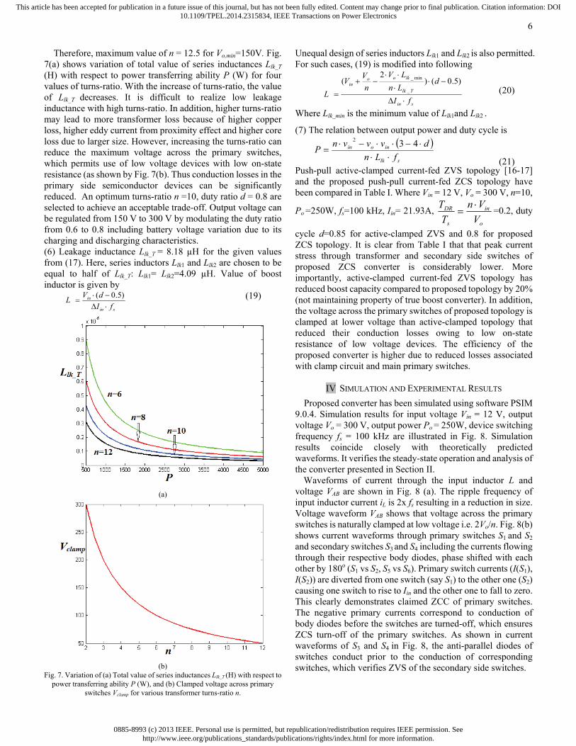
Therefore, maximum value of n = 12.5 for Vo,min=150V. Fig. 7(a) shows variation of total value of series inductances Llk_T
(H) with respect to power transferring ability P (W) for four values of turns-ratio. With the increase of turns-ratio, the value of Llk_T decreases. It is difficult to realize low leakage inductance with high turns-ratio. In addition, higher turns-ratio may lead to more transformer loss because of higher copper loss, higher eddy current from proximity effect and higher core loss due to larger size. However, increasing the turns-ratio can reduce the maximum voltage across the primary switches, which permits use of low voltage devices with low on-state resistance (as shown by Fig. 7(b). Thus conduction losses in the primary side semiconductor devices can be significantly reduced. An optimum turns-ratio n =10, duty ratio d = 0.8 are selected to achieve an acceptable trade-off. Output voltage can be regulated from 150 V to 300 V by modulating the duty ratio from 0.6 to 0.8 including battery voltage variation due to its charging and discharging characteristics. (6) Leakage inductance Llk_T = 8.18 µH for the given values from (17). Here, series inductors Llk1 and Llk2 are chosen to be equal to half of Llk_T: Llk1= Llk2=4.09 µH. Value of boost inductor is given by
sin
in
fI
dVL
)5.0( (19)
(a)
(b) Fig. 7. Variation of (a) Total value of series inductances Llk_T (H) with respect to
power transferring ability P (W), and (b) Clamped voltage across primary switches Vclamp for various transformer turns-ratio n.
Unequal design of series inductors Llk1 and Llk2 is also permitted. For such cases, (19) is modified into following
sin
Tlk
lkooin
fI
dLn
LV
n
VV
L
)5.0()2
(_
min_
(20)
Where Llk_min is the minimum value of Llk1and Llk2 .
(7) The relation between output power and duty cycle is
slk
inoin
fLn
dvvvnP
432
(21) Push-pull active-clamped current-fed ZVS topology [16-17] and the proposed push-pull current-fed ZCS topology have been compared in Table I. Where Vin = 12 V, Vo = 300 V, n=10,
Po =250W, fs=100 kHz, Iin= 21.93A, o
in
s
DR
V
Vn
T
T =0.2, duty
cycle d=0.85 for active-clamped ZVS and 0.8 for proposed ZCS topology. It is clear from Table I that that peak current stress through transformer and secondary side switches of proposed ZCS converter is considerably lower. More importantly, active-clamped current-fed ZVS topology has reduced boost capacity compared to proposed topology by 20% (not maintaining property of true boost converter). In addition, the voltage across the primary switches of proposed topology is clamped at lower voltage than active-clamped topology that reduced their conduction losses owing to low on-state resistance of low voltage devices. The efficiency of the proposed converter is higher due to reduced losses associated with clamp circuit and main primary switches.
IV SIMULATION AND EXPERIMENTAL RESULTS
Proposed converter has been simulated using software PSIM 9.0.4. Simulation results for input voltage Vin = 12 V, output voltage Vo = 300 V, output power Po = 250W, device switching frequency fs = 100 kHz are illustrated in Fig. 8. Simulation results coincide closely with theoretically predicted waveforms. It verifies the steady-state operation and analysis of the converter presented in Section II.
Waveforms of current through the input inductor L and voltage VAB are shown in Fig. 8 (a). The ripple frequency of input inductor current iL is 2x fs resulting in a reduction in size. Voltage waveform VAB shows that voltage across the primary switches is naturally clamped at low voltage i.e. 2Vo/n. Fig. 8(b) shows current waveforms through primary switches S1 and S2 and secondary switches S3 and S4 including the currents flowing through their respective body diodes, phase shifted with each other by 180o (S1 vs S2, S5 vs S6). Primary switch currents (I(S1), I(S2)) are diverted from one switch (say S1) to the other one (S2) causing one switch to rise to Iin and the other one to fall to zero. This clearly demonstrates claimed ZCC of primary switches. The negative primary currents correspond to conduction of body diodes before the switches are turned-off, which ensures ZCS turn-off of the primary switches. As shown in current waveforms of S3 and S4 in Fig. 8, the anti-parallel diodes of switches conduct prior to the conduction of corresponding switches, which verifies ZVS of the secondary side switches.
0885-8993 (c) 2013 IEEE. Personal use is permitted, but republication/redistribution requires IEEE permission. Seehttp://www.ieee.org/publications_standards/publications/rights/index.html for more information.
This article has been accepted for publication in a future issue of this journal, but has not been fully edited. Content may change prior to final publication. Citation information: DOI10.1109/TPEL.2014.2315834, IEEE Transactions on Power Electronics
7
(a)
(b)
Fig. 8. Simulation results for output power of 250W at 300V. (a) Current through input inductor iL and voltage VAB. (b) Primary switches currents iS1 and iS2 and secondary switches currents iS3 and iS4.
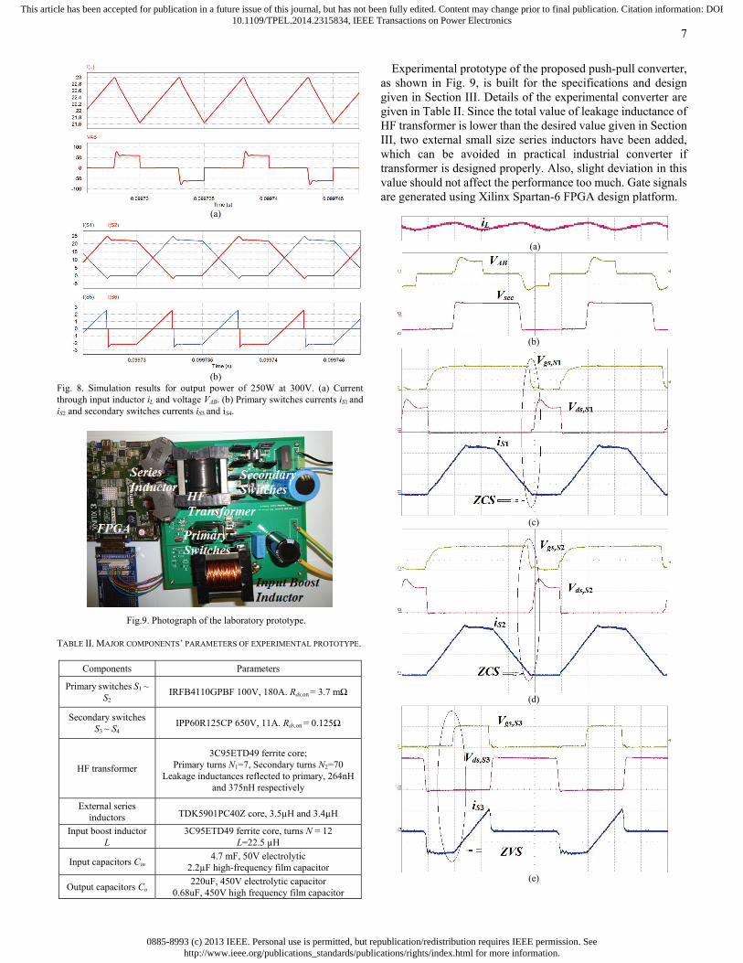
Fig.9. Photograph of the laboratory prototype.
TABLE II. MAJOR COMPONENTS’ PARAMETERS OF EXPERIMENTAL PROTOTYPE.
Components Parameters
Primary switches S1 ~ S2
IRFB4110GPBF 100V, 180A. Rds,on = 3.7 mΩ
Secondary switches S3 ~ S4
IPP60R125CP 650V, 11A. Rds,on = 0.125Ω
HF transformer
3C95ETD49 ferrite core; Primary turns N1=7, Secondary turns N2=70
Leakage inductances reflected to primary, 264nH and 375nH respectively
External series inductors TDK5901PC40Z core, 3.5µH and 3.4µH
Input boost inductor L
3C95ETD49 ferrite core, turns N = 12 L=22.5 µH
Input capacitors Cin 4.7 mF, 50V electrolytic
2.2µF high-frequency film capacitor
Output capacitors Co 220uF, 450V electrolytic capacitor
0.68uF, 450V high frequency film capacitor
Experimental prototype of the proposed push-pull converter, as shown in Fig. 9, is built for the specifications and design given in Section III. Details of the experimental converter are given in Table II. Since the total value of leakage inductance of HF transformer is lower than the desired value given in Section III, two external small size series inductors have been added, which can be avoided in practical industrial converter if transformer is designed properly. Also, slight deviation in this value should not affect the performance too much. Gate signals are generated using Xilinx Spartan-6 FPGA design platform.
(a)
(b)
(c)
(d)
(e)
0885-8993 (c) 2013 IEEE. Personal use is permitted, but republication/redistribution requires IEEE permission. Seehttp://www.ieee.org/publications_standards/publications/rights/index.html for more information.
This article has been accepted for publication in a future issue of this journal, but has not been fully edited. Content may change prior to final publication. Citation information: DOI10.1109/TPEL.2014.2315834, IEEE Transactions on Power Electronics
8
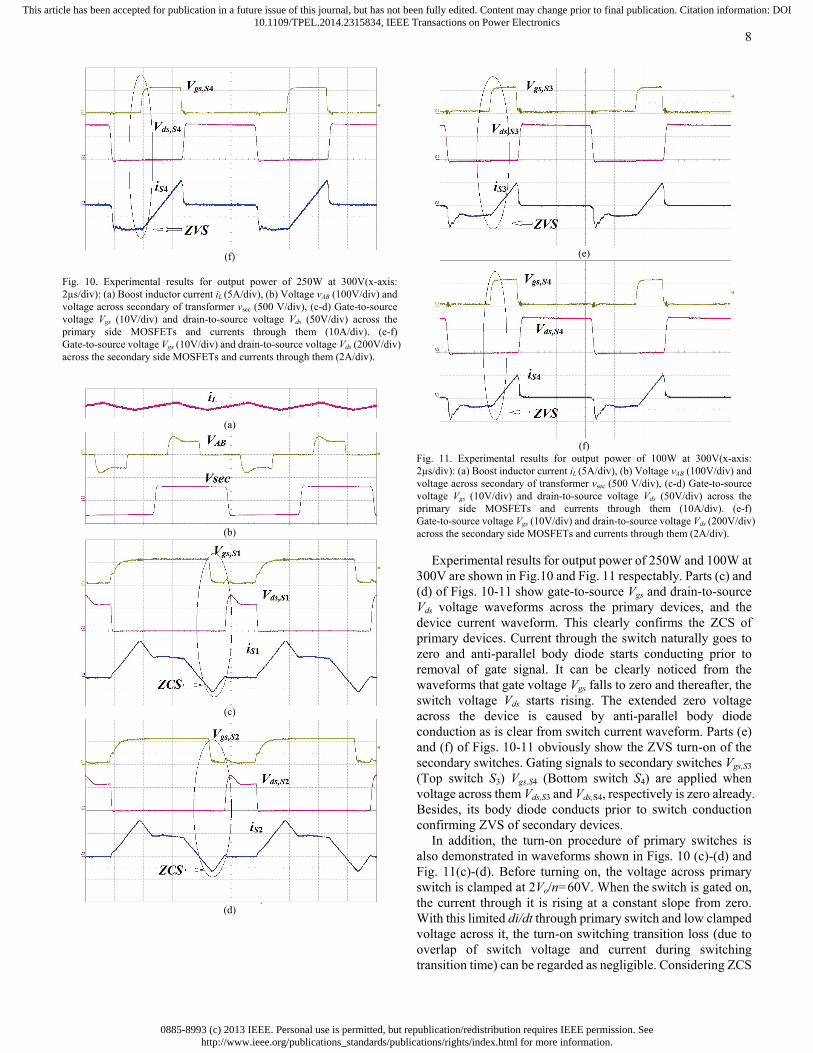
(f)
Fig. 10. Experimental results for output power of 250W at 300V(x-axis: 2µs/div): (a) Boost inductor current iL (5A/div), (b) Voltage vAB (100V/div) and voltage across secondary of transformer vsec (500 V/div), (c-d) Gate-to-source voltage Vgs (10V/div) and drain-to-source voltage Vds (50V/div) across the primary side MOSFETs and currents through them (10A/div). (e-f) Gate-to-source voltage Vgs (10V/div) and drain-to-source voltage Vds (200V/div) across the secondary side MOSFETs and currents through them (2A/div).
(a)
(b)
(c)
(d)
(e)
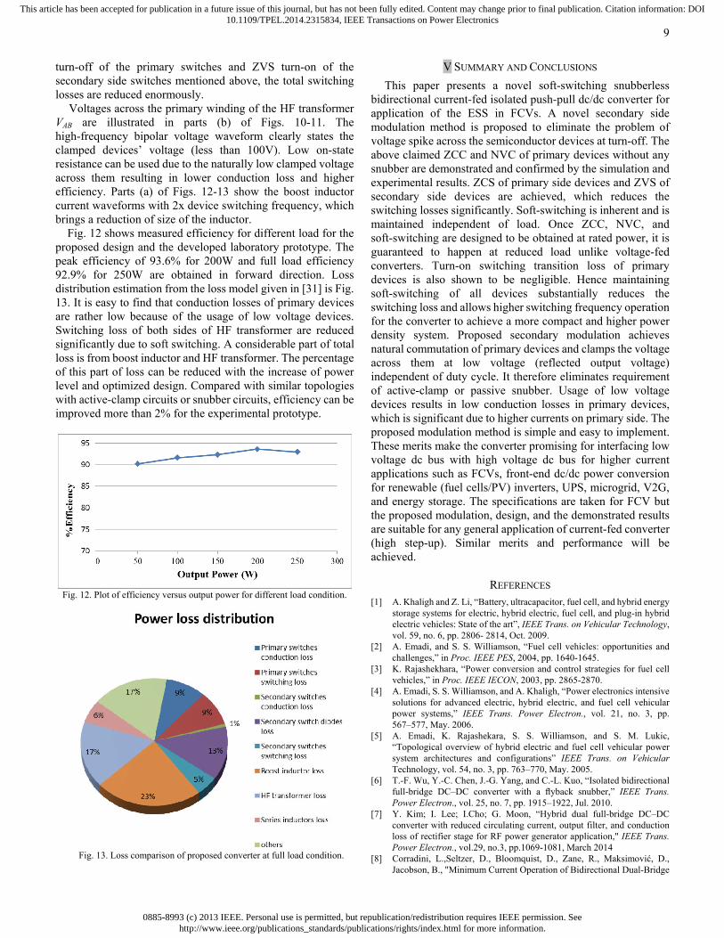
(f)
Fig. 11. Experimental results for output power of 100W at 300V(x-axis: 2µs/div): (a) Boost inductor current iL (5A/div), (b) Voltage vAB (100V/div) and voltage across secondary of transformer vsec (500 V/div), (c-d) Gate-to-source voltage Vgs (10V/div) and drain-to-source voltage Vds (50V/div) across the primary side MOSFETs and currents through them (10A/div). (e-f) Gate-to-source voltage Vgs (10V/div) and drain-to-source voltage Vds (200V/div) across the secondary side MOSFETs and currents through them (2A/div).
Experimental results for output power of 250W and 100W at 300V are shown in Fig.10 and Fig. 11 respectably. Parts (c) and (d) of Figs. 10-11 show gate-to-source Vgs and drain-to-source Vds voltage waveforms across the primary devices, and the device current waveform. This clearly confirms the ZCS of primary devices. Current through the switch naturally goes to zero and anti-parallel body diode starts conducting prior to removal of gate signal. It can be clearly noticed from the waveforms that gate voltage Vgs falls to zero and thereafter, the switch voltage Vds starts rising. The extended zero voltage across the device is caused by anti-parallel body diode conduction as is clear from switch current waveform. Parts (e) and (f) of Figs. 10-11 obviously show the ZVS turn-on of the secondary switches. Gating signals to secondary switches Vgs,S3 (Top switch S3) Vgs,S4 (Bottom switch S4) are applied when voltage across them Vds,S3 and Vds,S4, respectively is zero already. Besides, its body diode conducts prior to switch conduction confirming ZVS of secondary devices.
In addition, the turn-on procedure of primary switches is also demonstrated in waveforms shown in Figs. 10 (c)-(d) and Fig. 11(c)-(d). Before turning on, the voltage across primary switch is clamped at 2Vo/n=60V. When the switch is gated on, the current through it is rising at a constant slope from zero. With this limited di/dt through primary switch and low clamped voltage across it, the turn-on switching transition loss (due to overlap of switch voltage and current during switching transition time) can be regarded as negligible. Considering ZCS
0885-8993 (c) 2013 IEEE. Personal use is permitted, but republication/redistribution requires IEEE permission. Seehttp://www.ieee.org/publications_standards/publications/rights/index.html for more information.
This article has been accepted for publication in a future issue of this journal, but has not been fully edited. Content may change prior to final publication. Citation information: DOI10.1109/TPEL.2014.2315834, IEEE Transactions on Power Electronics
9
turn-off of the primary switches and ZVS turn-on of the secondary side switches mentioned above, the total switching losses are reduced enormously.
Voltages across the primary winding of the HF transformer VAB are illustrated in parts (b) of Figs. 10-11. The high-frequency bipolar voltage waveform clearly states the clamped devices’ voltage (less than 100V). Low on-state resistance can be used due to the naturally low clamped voltage across them resulting in lower conduction loss and higher efficiency. Parts (a) of Figs. 12-13 show the boost inductor current waveforms with 2x device switching frequency, which brings a reduction of size of the inductor.
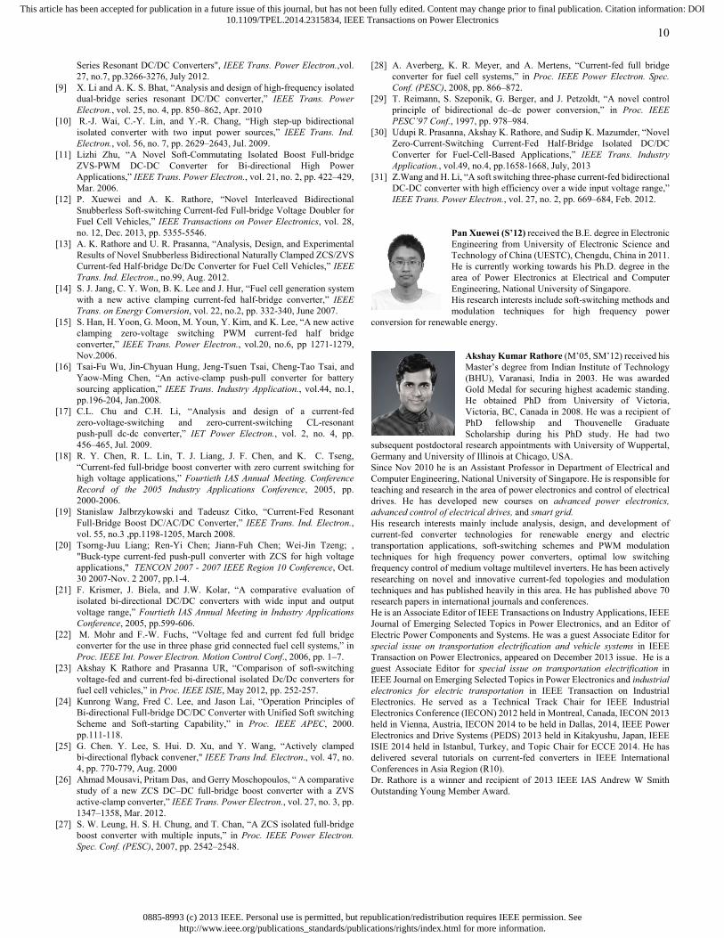
Fig. 12 shows measured efficiency for different load for the proposed design and the developed laboratory prototype. The peak efficiency of 93.6% for 200W and full load efficiency 92.9% for 250W are obtained in forward direction. Loss distribution estimation from the loss model given in [31] is Fig. 13. It is easy to find that conduction losses of primary devices are rather low because of the usage of low voltage devices. Switching loss of both sides of HF transformer are reduced significantly due to soft switching. A considerable part of total loss is from boost inductor and HF transformer. The percentage of this part of loss can be reduced with the increase of power level and optimized design. Compared with similar topologies with active-clamp circuits or snubber circuits, efficiency can be improved more than 2% for the experimental prototype.
Fig. 12. Plot of efficiency versus output power for different load condition.
Fig. 13. Loss comparison of proposed converter at full load condition.
V SUMMARY AND CONCLUSIONS
This paper presents a novel soft-switching snubberless bidirectional current-fed isolated push-pull dc/dc converter for application of the ESS in FCVs. A novel secondary side modulation method is proposed to eliminate the problem of voltage spike across the semiconductor devices at turn-off. The above claimed ZCC and NVC of primary devices without any snubber are demonstrated and confirmed by the simulation and experimental results. ZCS of primary side devices and ZVS of secondary side devices are achieved, which reduces the switching losses significantly. Soft-switching is inherent and is maintained independent of load. Once ZCC, NVC, and soft-switching are designed to be obtained at rated power, it is guaranteed to happen at reduced load unlike voltage-fed converters. Turn-on switching transition loss of primary devices is also shown to be negligible. Hence maintaining soft-switching of all devices substantially reduces the switching loss and allows higher switching frequency operation for the converter to achieve a more compact and higher power density system. Proposed secondary modulation achieves natural commutation of primary devices and clamps the voltage across them at low voltage (reflected output voltage) independent of duty cycle. It therefore eliminates requirement of active-clamp or passive snubber. Usage of low voltage devices results in low conduction losses in primary devices, which is significant due to higher currents on primary side. The proposed modulation method is simple and easy to implement. These merits make the converter promising for interfacing low voltage dc bus with high voltage dc bus for higher current applications such as FCVs, front-end dc/dc power conversion for renewable (fuel cells/PV) inverters, UPS, microgrid, V2G, and energy storage. The specifications are taken for FCV but the proposed modulation, design, and the demonstrated results are suitable for any general application of current-fed converter (high step-up). Similar merits and performance will be achieved.
REFERENCES [1] A. Khaligh and Z. Li, “Battery, ultracapacitor, fuel cell, and hybrid energy
storage systems for electric, hybrid electric, fuel cell, and plug-in hybrid electric vehicles: State of the art”, IEEE Trans. on Vehicular Technology, vol. 59, no. 6, pp. 2806- 2814, Oct. 2009.
[2] A. Emadi, and S. S. Williamson, “Fuel cell vehicles: opportunities and challenges,” in Proc. IEEE PES, 2004, pp. 1640-1645.
[3] K. Rajashekhara, “Power conversion and control strategies for fuel cell vehicles,” in Proc. IEEE IECON, 2003, pp. 2865-2870.
[4] A. Emadi, S. S. Williamson, and A. Khaligh, “Power electronics intensive solutions for advanced electric, hybrid electric, and fuel cell vehicular power systems,” IEEE Trans. Power Electron., vol. 21, no. 3, pp. 567–577, May. 2006.
[5] A. Emadi, K. Rajashekara, S. S. Williamson, and S. M. Lukic, “Topological overview of hybrid electric and fuel cell vehicular power system architectures and configurations” IEEE Trans. on Vehicular Technology, vol. 54, no. 3, pp. 763–770, May. 2005.
[6] T.-F. Wu, Y.-C. Chen, J.-G. Yang, and C.-L. Kuo, “Isolated bidirectional full-bridge DC–DC converter with a flyback snubber,” IEEE Trans. Power Electron., vol. 25, no. 7, pp. 1915–1922, Jul. 2010.
[7] Y. Kim; I. Lee; I.Cho; G. Moon, “Hybrid dual full-bridge DC–DC converter with reduced circulating current, output filter, and conduction loss of rectifier stage for RF power generator application," IEEE Trans. Power Electron., vol.29, no.3, pp.1069-1081, March 2014
[8] Corradini, L.,Seltzer, D., Bloomquist, D., Zane, R., Maksimović, D., Jacobson, B., "Minimum Current Operation of Bidirectional Dual-Bridge
0885-8993 (c) 2013 IEEE. Personal use is permitted, but republication/redistribution requires IEEE permission. Seehttp://www.ieee.org/publications_standards/publications/rights/index.html for more information.
This article has been accepted for publication in a future issue of this journal, but has not been fully edited. Content may change prior to final publication. Citation information: DOI10.1109/TPEL.2014.2315834, IEEE Transactions on Power Electronics
10
Series Resonant DC/DC Converters", IEEE Trans. Power Electron.,vol. 27, no.7, pp.3266-3276, July 2012.
[9] X. Li and A. K. S. Bhat, “Analysis and design of high-frequency isolated dual-bridge series resonant DC/DC converter,” IEEE Trans. Power Electron., vol. 25, no. 4, pp. 850–862, Apr. 2010
[10] R.-J. Wai, C.-Y. Lin, and Y.-R. Chang, “High step-up bidirectional isolated converter with two input power sources,” IEEE Trans. Ind. Electron., vol. 56, no. 7, pp. 2629–2643, Jul. 2009.
[11] Lizhi Zhu, “A Novel Soft-Commutating Isolated Boost Full-bridge ZVS-PWM DC-DC Converter for Bi-directional High Power Applications,” IEEE Trans. Power Electron., vol. 21, no. 2, pp. 422–429, Mar. 2006.
[12] P. Xuewei and A. K. Rathore, “Novel Interleaved Bidirectional Snubberless Soft-switching Current-fed Full-bridge Voltage Doubler for Fuel Cell Vehicles,” IEEE Transactions on Power Electronics, vol. 28, no. 12, Dec. 2013, pp. 5355-5546.
[13] A. K. Rathore and U. R. Prasanna, “Analysis, Design, and Experimental Results of Novel Snubberless Bidirectional Naturally Clamped ZCS/ZVS Current-fed Half-bridge Dc/Dc Converter for Fuel Cell Vehicles,” IEEE Trans. Ind. Electron., no.99, Aug. 2012.
[14] S. J. Jang, C. Y. Won, B. K. Lee and J. Hur, “Fuel cell generation system with a new active clamping current-fed half-bridge converter,” IEEE Trans. on Energy Conversion, vol. 22, no.2, pp. 332-340, June 2007.
[15] S. Han, H. Yoon, G. Moon, M. Youn, Y. Kim, and K. Lee, “A new active clamping zero-voltage switching PWM current-fed half bridge converter,” IEEE Trans. Power Electron., vol.20, no.6, pp 1271-1279, Nov.2006.
[16] Tsai-Fu Wu, Jin-Chyuan Hung, Jeng-Tsuen Tsai, Cheng-Tao Tsai, and Yaow-Ming Chen, “An active-clamp push-pull converter for battery sourcing application,” IEEE Trans. Industry Application., vol.44, no.1, pp.196-204, Jan.2008.
[17] C.L. Chu and C.H. Li, “Analysis and design of a current-fed zero-voltage-switching and zero-current-switching CL-resonant push-pull dc-dc converter,” IET Power Electron., vol. 2, no. 4, pp. 456–465, Jul. 2009.
[18] R. Y. Chen, R. L. Lin, T. J. Liang, J. F. Chen, and K. C. Tseng, “Current-fed full-bridge boost converter with zero current switching for high voltage applications,” Fourtieth IAS Annual Meeting. Conference Record of the 2005 Industry Applications Conference, 2005, pp. 2000-2006.
[19] Stanislaw Jalbrzykowski and Tadeusz Citko, “Current-Fed Resonant Full-Bridge Boost DC/AC/DC Converter,” IEEE Trans. Ind. Electron., vol. 55, no.3 ,pp.1198-1205, March 2008.
[20] Tsorng-Juu Liang; Ren-Yi Chen; Jiann-Fuh Chen; Wei-Jin Tzeng; , "Buck-type current-fed push-pull converter with ZCS for high voltage applications," TENCON 2007 - 2007 IEEE Region 10 Conference, Oct. 30 2007-Nov. 2 2007, pp.1-4.
[21] F. Krismer, J. Biela, and J.W. Kolar, “A comparative evaluation of isolated bi-directional DC/DC converters with wide input and output voltage range,” Fourtieth IAS Annual Meeting in Industry Applications Conference, 2005, pp.599-606.
[22] M. Mohr and F.-W. Fuchs, “Voltage fed and current fed full bridge converter for the use in three phase grid connected fuel cell systems,” in Proc. IEEE Int. Power Electron. Motion Control Conf., 2006, pp. 1–7.
[23] Akshay K Rathore and Prasanna UR, “Comparison of soft-switching voltage-fed and current-fed bi-directional isolated Dc/Dc converters for fuel cell vehicles,” in Proc. IEEE ISIE, May 2012, pp. 252-257.
[24] Kunrong Wang, Fred C. Lee, and Jason Lai, “Operation Principles of Bi-directional Full-bridge DC/DC Converter with Unified Soft switching Scheme and Soft-starting Capability,” in Proc. IEEE APEC, 2000. pp.111-118.
[25] G. Chen. Y. Lee, S. Hui. D. Xu, and Y. Wang, “Actively clamped bi-directional flyback convener," IEEE Trans Ind. Electron., vol. 47, no. 4, pp. 770-779, Aug. 2000
[26] Ahmad Mousavi, Pritam Das, and Gerry Moschopoulos, “ A comparative study of a new ZCS DC–DC full-bridge boost converter with a ZVS active-clamp converter,” IEEE Trans. Power Electron., vol. 27, no. 3, pp. 1347–1358, Mar. 2012.
[27] S. W. Leung, H. S. H. Chung, and T. Chan, “A ZCS isolated full-bridge boost converter with multiple inputs,” in Proc. IEEE Power Electron. Spec. Conf. (PESC), 2007, pp. 2542–2548.
[28] A. Averberg, K. R. Meyer, and A. Mertens, “Current-fed full bridge converter for fuel cell systems,” in Proc. IEEE Power Electron. Spec. Conf. (PESC), 2008, pp. 866–872.
[29] T. Reimann, S. Szeponik, G. Berger, and J. Petzoldt, “A novel control principle of bidirectional dc–dc power conversion,” in Proc. IEEE PESC’97 Conf., 1997, pp. 978–984.
[30] Udupi R. Prasanna, Akshay K. Rathore, and Sudip K. Mazumder, “Novel Zero-Current-Switching Current-Fed Half-Bridge Isolated DC/DC Converter for Fuel-Cell-Based Applications,” IEEE Trans. Industry Application., vol.49, no.4, pp.1658-1668, July, 2013
[31] Z.Wang and H. Li, “A soft switching three-phase current-fed bidirectional DC-DC converter with high efficiency over a wide input voltage range,” IEEE Trans. Power Electron., vol. 27, no. 2, pp. 669–684, Feb. 2012.
Pan Xuewei (S’12) received the B.E. degree in Electronic Engineering from University of Electronic Science and Technology of China (UESTC), Chengdu, China in 2011. He is currently working towards his Ph.D. degree in the area of Power Electronics at Electrical and Computer Engineering, National University of Singapore. His research interests include soft-switching methods and modulation techniques for high frequency power
conversion for renewable energy.
Akshay Kumar Rathore (M’05, SM’12) received his Master’s degree from Indian Institute of Technology (BHU), Varanasi, India in 2003. He was awarded Gold Medal for securing highest academic standing. He obtained PhD from University of Victoria, Victoria, BC, Canada in 2008. He was a recipient of PhD fellowship and Thouvenelle Graduate Scholarship during his PhD study. He had two
subsequent postdoctoral research appointments with University of Wuppertal, Germany and University of Illinois at Chicago, USA. Since Nov 2010 he is an Assistant Professor in Department of Electrical and Computer Engineering, National University of Singapore. He is responsible for teaching and research in the area of power electronics and control of electrical drives. He has developed new courses on advanced power electronics, advanced control of electrical drives, and smart grid. His research interests mainly include analysis, design, and development of current-fed converter technologies for renewable energy and electric transportation applications, soft-switching schemes and PWM modulation techniques for high frequency power converters, optimal low switching frequency control of medium voltage multilevel inverters. He has been actively researching on novel and innovative current-fed topologies and modulation techniques and has published heavily in this area. He has published above 70 research papers in international journals and conferences. He is an Associate Editor of IEEE Transactions on Industry Applications, IEEE Journal of Emerging Selected Topics in Power Electronics, and an Editor of Electric Power Components and Systems. He was a guest Associate Editor for special issue on transportation electrification and vehicle systems in IEEE Transaction on Power Electronics, appeared on December 2013 issue. He is a guest Associate Editor for special issue on transportation electrification in IEEE Journal on Emerging Selected Topics in Power Electronics and industrial electronics for electric transportation in IEEE Transaction on Industrial Electronics. He served as a Technical Track Chair for IEEE Industrial Electronics Conference (IECON) 2012 held in Montreal, Canada, IECON 2013 held in Vienna, Austria, IECON 2014 to be held in Dallas, 2014, IEEE Power Electronics and Drive Systems (PEDS) 2013 held in Kitakyushu, Japan, IEEE ISIE 2014 held in Istanbul, Turkey, and Topic Chair for ECCE 2014. He has delivered several tutorials on current-fed converters in IEEE International Conferences in Asia Region (R10). Dr. Rathore is a winner and recipient of 2013 IEEE IAS Andrew W Smith Outstanding Young Member Award.