Embed Size (px)
Citation preview
HAL Id: hal-00472593https://hal.archives-ouvertes.fr/hal-00472593
Submitted on 12 Apr 2010
HAL is a multi-disciplinary open accessarchive for the deposit and dissemination of sci-entific research documents, whether they are pub-lished or not. The documents may come fromteaching and research institutions in France orabroad, or from public or private research centers.
L’archive ouverte pluridisciplinaire HAL, estdestinée au dépôt et à la diffusion de documentsscientifiques de niveau recherche, publiés ou non,émanant des établissements d’enseignement et derecherche français ou étrangers, des laboratoirespublics ou privés.
Near-field observation of surface plasmon polaritonpropagation on thin metal stripes
J. C. Weeber, J. R. Krenn, Alain Dereux, B. Lamprecht, Y. Lacroute, J. P.Goudonnet
To cite this version:J. C. Weeber, J. R. Krenn, Alain Dereux, B. Lamprecht, Y. Lacroute, et al.. Near-field observation ofsurface plasmon polariton propagation on thin metal stripes. Physical Review B: Condensed Matterand Materials Physics (1998-2015), American Physical Society, 2001, 64 (4), pp.045411. �hal-00472593�
Near–field observation of surface plasmon polariton propagation
on thin metal stripes.
J-C. Weeber, J. R. Krenn(†), A. Dereux, B. Lamprecht(†), Y. Lacroute and J. P. Goudonnet
Laboratoire de Physique de l’Universite de Bourgogne, Optique Submicronique, BP 47870,
F-21078 Dijon, France
(†) Institut fur Experimentalphysik, Universitat Graz,Universitatsplatz 5, A-8010 Graz, Austria
(May 22, 2001)
Abstract
We use a Photon Scanning Tunneling Microscope to probe the field of sur-
face plasmon polaritons modes excited on finite width thin metal films (metal
stripes). We first investigate the coupling between surface plasmons launched
by a focused beam on a homogeneous thin film and the modes sustained by
metal stripes of different widths. We show that, if the width of the metal
stripe is about a few microns, a strong coupling with the stripe modes can be
achieved at visible frequencies. A sharp transverse confinement of the field
associated to the surface plasmon modes propagating on the metal stripe is
unambiguously observed on the constant height Photon Scanning Tunneling
Microscope (PSTM) images. The back–reflection of theses modes at the end
of the stripe leads to a surface–wave interference pattern from which the wave-
length of the stripe surface plasmon modes is directly measured. We finally
demonstrate that metal stripes could be used for optical addressing purposes
at the micron scale since a stripe with a triangularly shaped termination per-
forms the focusing of the stripe surface plasmon field.
1

PACS:
78.66.-w Optical properties of specific thin films, surfaces, and low- dimen-
sional structures
71.36.+c Polaritons
07.79.Fc Near-field scanning optical microscopes
Typeset using REVTEX
2
I. INTRODUCTION
Surface Plasmon Polaritons (SPP) are electromagnetic modes existing at the interface
between a metal and a dielectric material [1]. SPP modes can propagate along the metal–air
interface over a finite length depending on the ohmic losses of the metal. Theoretically, a
typical mean–free path of a few tens of micrometers can be achieved at visible frequencies.
The most common technique to excite a SPP at a metal-air interface consists in evaporating
a thin metal film onto an optically dense substrate. Illuminating through the substrate at
an angle of incidence slightly larger than the critical angle for total internal reflection allows
the wave–vector of the incident light to match the one of the SPP. This technique known
as Attenuated Total Reflection (ATR) leads to an illumination of the thin film similar to
the usual illumination conditions of a sample observed with a Photon Scanning Tunneling
Microscope (PSTM) [2]. Therefore, the PSTM turns out to be an efficient tool to investigate,
in direct space, SPP excited in the ATR configuration. During the last decade, several works
have demonstrated the capabilities of the PSTM to probe SPP in the near–field zone. For
example, the first direct observation of SPP propagation along a silver-air interface can be
found in Ref. [3]. More recently, elastic SPP scattering on individual surface defects has
been reported in Refs [4–6]. However, in all the previously cited works, the SPP was excited
on thin metal films of infinite widths. Up to now very little is known about the near–field
behavior of a SPP launched on a finite width thin metal film (metal stripe).
In this work, we use a PSTM to perform what we believe to be the first near–field
observations of SPP modes excited, at a visible frequency, on a metal stripe with a width in
the range of a few micrometers. The excitation of SPP modes on a metal stripe is not only
of fundamental interest but may have also practical applications. Indeed, on the basis of
theoretical results and of far–field measurements, it has been shown very recently that thin
metal stripes, embedded in a homogeneous dielectric and supporting long–range SPP modes,
could be used as waveguides at optical telecommunication frequencies [7–9]. In this work,
since we are concerned with metal stripes deposited on a glass substrate, the excitation of
3
long–range SPP modes is not expected. Accordingly, a propagation length large enough to
be useful for large scale integrated optics purposes seems rather unrealistic. However, the
structures we consider provide an easy route to achieve the optical addressing by a surface–
wave of objects deposited on a substrate such as metal nano-particles or even molecules. In
the context of near–field optical microscopy, these features may be of experimental interest
to investigate the near–field response of single objects.
The paper is organized as follows. In section II, we describe the experimental set–up we
have used to obtain the constant height PSTM images. In section III, we investigate the
behavior of a SPP excited by the focused gaussian beam on a thin film area with lateral
dimensions much larger than the incident spot. In section IV, the coupling between the
modes sustained by stripes of different widths and a SPP launched on the homogeneous thin
film is considered. Specifically, the influence of an azimuthal or lateral misalignement of the
incident beam with the axis of the stripe is discussed. Having in mind to use metal stripes
for optical addressing applications, we consider in section V the capability of a triangulary
shaped stripe termination to focus the field of a surface plasmon mode excited by shining
the incident beam directly on a stripe. Finally, concluding remarks are given in section VI.
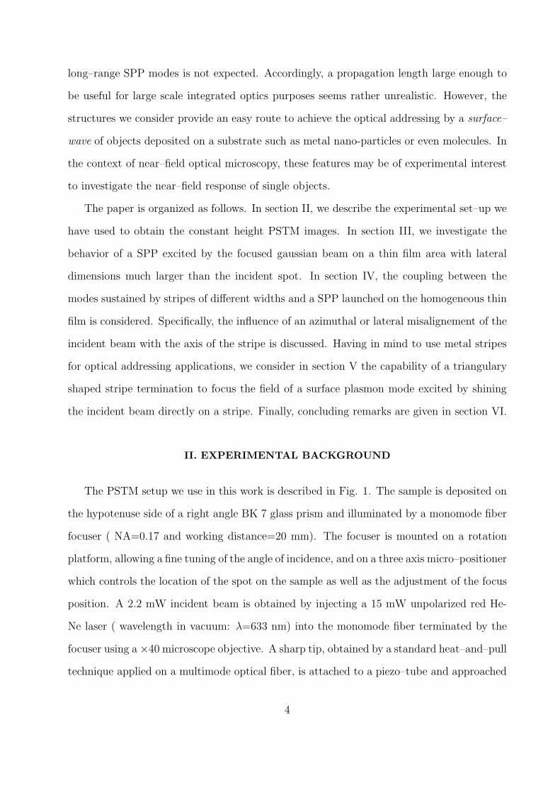
II. EXPERIMENTAL BACKGROUND
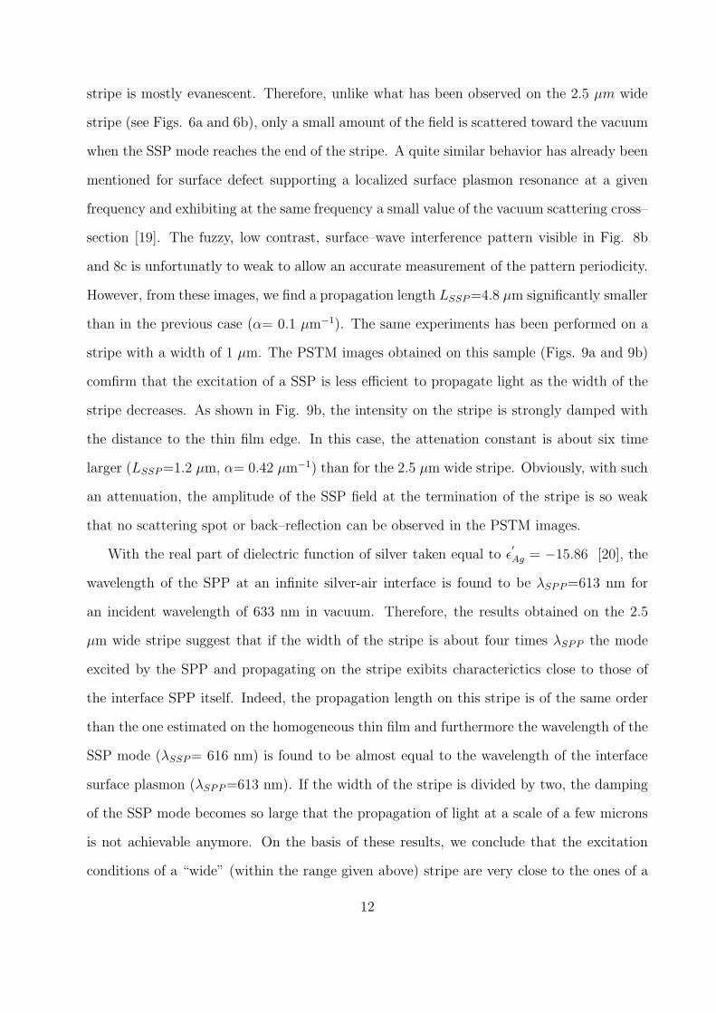
The PSTM setup we use in this work is described in Fig. 1. The sample is deposited on
the hypotenuse side of a right angle BK 7 glass prism and illuminated by a monomode fiber
focuser ( NA=0.17 and working distance=20 mm). The focuser is mounted on a rotation
platform, allowing a fine tuning of the angle of incidence, and on a three axis micro–positioner
which controls the location of the spot on the sample as well as the adjustment of the focus
position. A 2.2 mW incident beam is obtained by injecting a 15 mW unpolarized red He-
Ne laser ( wavelength in vacuum: λ=633 nm) into the monomode fiber terminated by the
focuser using a ×40 microscope objective. A sharp tip, obtained by a standard heat–and–pull
technique applied on a multimode optical fiber, is attached to a piezo–tube and approached
4
to the immediate vicinity of the sample surface in order to collect the optical near–field
resulting from the illumination of the sample. The optical signal picked-up by the fiber–tip
is then converted by a photo-multiplier tube and amplified in a current/voltage amplifier.
When the tip is scanned at constant height in the near–field zone, the signal collected by the
probe provides the spatial distribution of the optical near–field intensity in a plane parallel
to the sample surface.
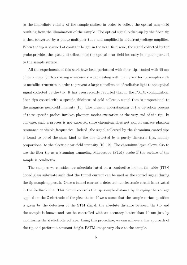
All the experiments of this work have been performed with fiber–tips coated with 15 nm
of chromium. Such a coating is necessary when dealing with highly scattering samples such
as metallic structures in order to prevent a large contribution of radiative light to the optical
signal collected by the tip. It has been recently reported that in the PSTM configuration,
fiber–tips coated with a specific thickness of gold collect a signal that is proportional to
the magnetic near-field intensity [10]. The present understanding of the detection process
of these specific probes involves plasmon modes excitation at the very end of the tip. In
our case, such a process is not expected since chromium does not exhibit surface plasmon
resonance at visible frequencies. Indeed, the signal collected by the chromium coated tips
is found to be of the same kind as the one detected by a purely dielectric tips, namely
proportional to the electric near–field intensity [10–12]. The chromium layer allows also to
use the fiber tip as a Scanning Tunneling Microscope (STM) probe if the surface of the
sample is conductive.
The samples we consider are microfabricated on a conductive indium-tin-oxide (ITO)
doped glass substrate such that the tunnel current can be used as the control signal during
the tip-sample approach. Once a tunnel current is detected, an electronic circuit is activated
in the feedback line. This circuit controls the tip–sample distance by changing the voltage
applied on the Z electrode of the piezo–tube. If we assume that the sample surface position
is given by the detection of the STM signal, the absolute distance between the tip and
the sample is known and can be controlled with an accuracy better than 10 nm just by
monitoring the Z electrode voltage. Using this procedure, we can achieve a fine approach of
the tip and perform a constant height PSTM image very close to the sample.
5
III. SURFACE PLASMON POLARITON EXCITATION WITH A FOCUSED
BEAM
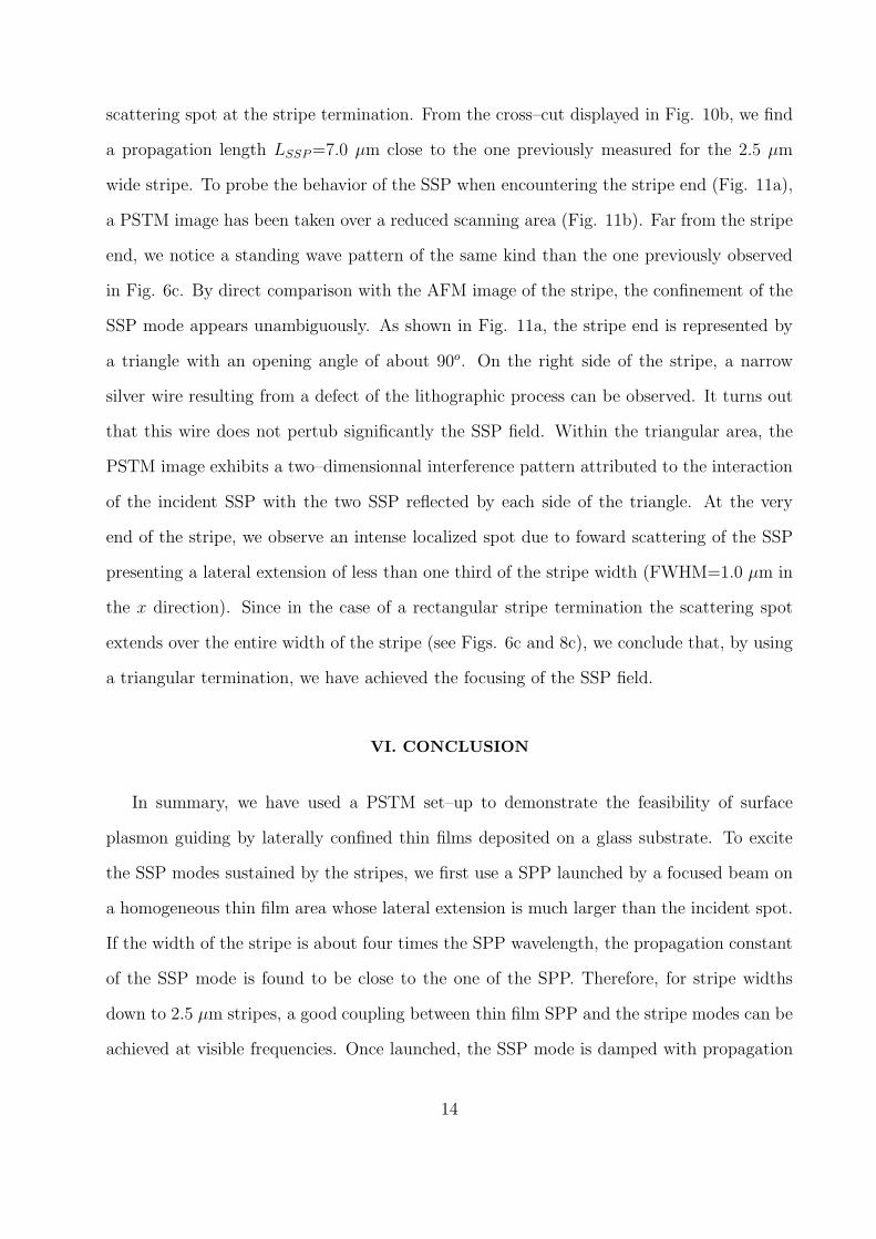
The first sample we consider has been designed to investigate the coupling between
the surface plasmon modes supported by a metal stripe and a classical SPP excited on
a homogeneous thin film area. The sample has been realized by standard electron–beam
lithography technique on a ITO glass substrate covered with a spin-coated, 200 nm thick,
polymethylmeta acrylate (PMMA) layer. After the lithography process, a silver film with
a thickness of 60 nm has been deposited by sputtering onto the substrate. The root mean
square (RMS) roughness of the silver film as determined by Atomic Force Microscope (AFM)
imaging has been found to be about 2.5 nm. After the lift-off of the PMMA layer, the sample
shown in Fig. 2a has been obtained. The sample consists of a large thin film area to which
several silver stripes of different widths are connected. The lower face of the substrate has
been optically connected to the glass prism using an index matching oil such that the SPP
at the silver-air interface can be excited in the ATR configuration. If the polarizer mounted
on the focuser is rotated to align the electric field of the incident beam with the plane of
incidence (TM polarization), the SPP excitation on the thin film area is effective at an angle
of incidence of about 43o. Because we use a focused beam illumination, the SPP excitation
manifest itself as a dark line in the circular reflected spot observed at the exit face of the
prism. Obviously, this dark line is due to the absorption of the incident light travelling with
a parallel component of the wave-vector that matches the one of the SPP.
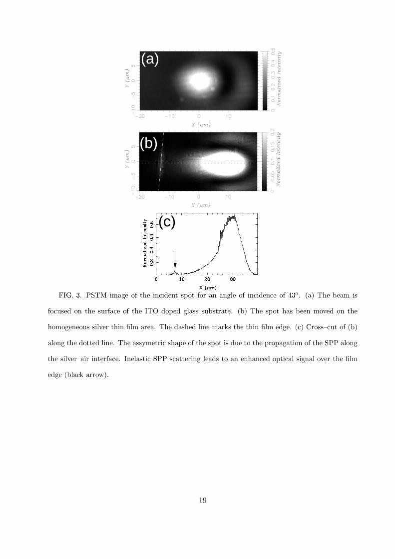
The two images shown in Fig. 3a and Fig. 3b have been obtained for an incident beam
respectively focused on the surface of the ITO substrate and on the homogeneous silver thin
film area. In both cases, the beam propagates from the right towards the left side in a
plane of incidence parallel to the x axis and impinges on the surface of the sample with an
angle of incidence of 43o. If located on the ITO substrate (Fig. 3a), the spot resulting from
the total internal reflection of the incident beam exhibits an almost circular shape. This
image, as well as all the PSTM images presented in this work, is normalized with respect to
6
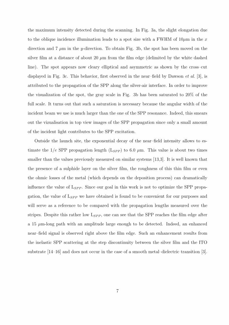
the maximum intensity detected during the scanning. In Fig. 3a, the slight elongation due
to the oblique incidence illumination leads to a spot size with a FWHM of 10µm in the x
direction and 7 µm in the y-direction. To obtain Fig. 3b, the spot has been moved on the
silver film at a distance of about 20 µm from the film edge (delimited by the white dashed
line). The spot appears now cleary elliptical and asymmetric as shown by the cross–cut
displayed in Fig. 3c. This behavior, first observed in the near–field by Dawson et al. [3], is
attributed to the propagation of the SPP along the silver-air interface. In order to improve
the visualization of the spot, the gray scale in Fig. 3b has been saturated to 20% of the
full scale. It turns out that such a saturation is necessary because the angular width of the
incident beam we use is much larger than the one of the SPP resonance. Indeed, this smears
out the vizualisation in top view images of the SPP propagation since only a small amount
of the incident light contributes to the SPP excitation.
Outside the launch site, the exponential decay of the near–field intensity allows to es-
timate the 1/e SPP propagation length (LSPP ) to 6.0 µm. This value is about two times
smaller than the values previously measured on similar systems [13,3]. It is well known that
the presence of a sulphide layer on the silver film, the roughness of this thin film or even
the ohmic losses of the metal (which depends on the deposition process) can dramatically
influence the value of LSPP . Since our goal in this work is not to optimize the SPP propa-
gation, the value of LSPP we have obtained is found to be convenient for our purposes and
will serve as a reference to be compared with the propagation lengths measured over the
stripes. Despite this rather low LSPP , one can see that the SPP reaches the film edge after
a 15 µm-long path with an amplitude large enough to be detected. Indeed, an enhanced
near–field signal is observed right above the film edge. Such an enhancement results from
the inelastic SPP scattering at the step discontinuity between the silver film and the ITO
substrate [14–16] and does not occur in the case of a smooth metal–dielectric transition [3].
7
IV. METAL STRIPES EXCITATION WITH A SURFACE PLASMON
POLARITON
In this section, we focus on the coupling between a SPP launched on the homogeneous
thin film area and the stripe surface plasmon (SSP) modes sustained by a metal thin film of
finite width.
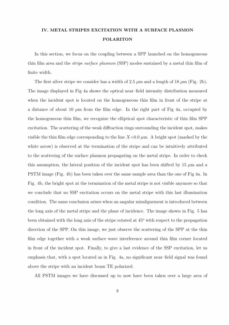
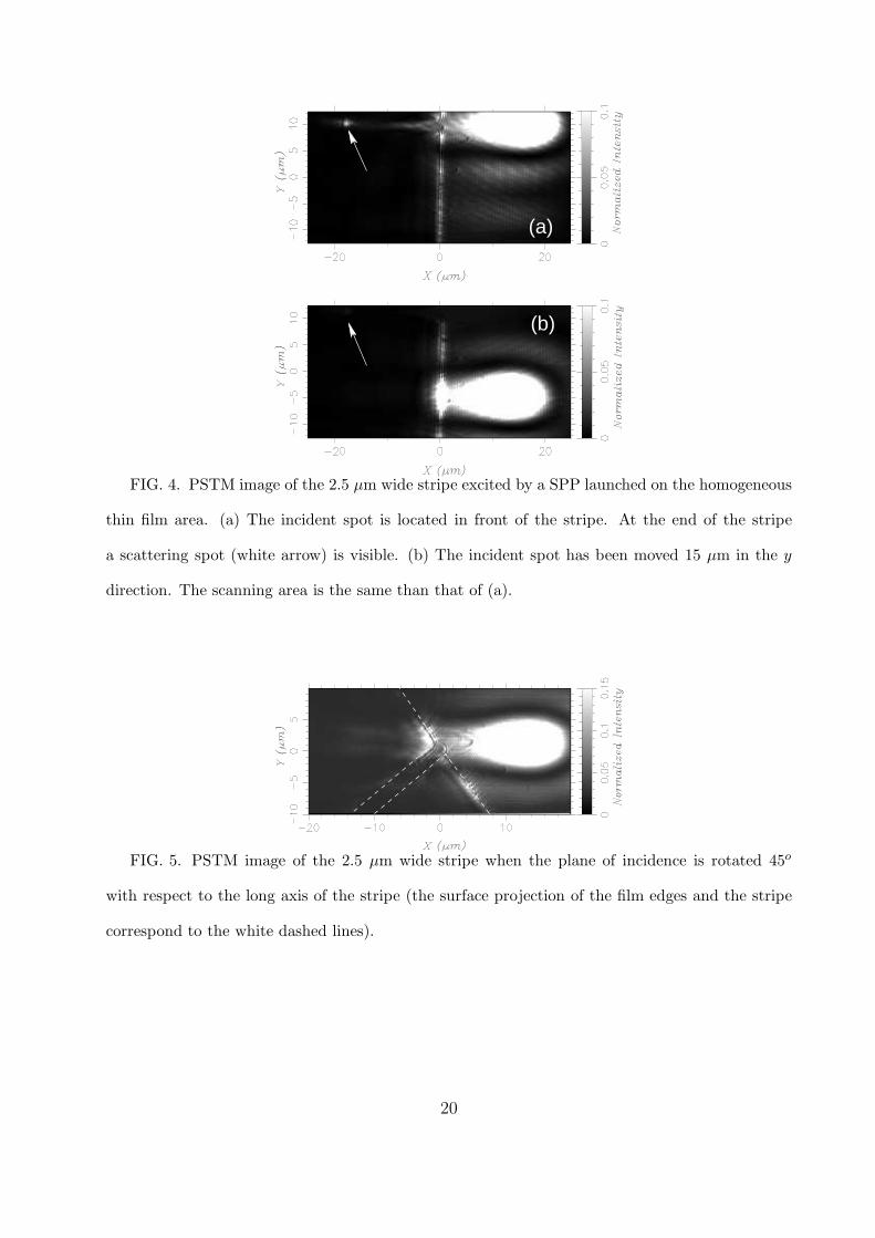
The first silver stripe we consider has a width of 2.5 µm and a length of 18 µm (Fig. 2b).
The image displayed in Fig 4a shows the optical near–field intensity distribution measured
when the incident spot is located on the homogeneous thin film in front of the stripe at
a distance of about 10 µm from the film edge. In the right part of Fig 4a, occupied by
the homogeneous thin film, we recognize the elliptical spot characteristic of thin film SPP
excitation. The scattering of the weak diffraction rings surrounding the incident spot, makes
visible the thin film edge corresponding to the line X=0.0 µm. A bright spot (marked by the
white arrow) is observed at the termination of the stripe and can be intuitively attributed
to the scattering of the surface plasmon propagating on the metal stripe. In order to check
this assumption, the lateral position of the incident spot has been shifted by 15 µm and a
PSTM image (Fig. 4b) has been taken over the same sample area than the one of Fig 4a. In
Fig. 4b, the bright spot at the termination of the metal stripe is not visible anymore so that
we conclude that no SSP excitation occurs on the metal stripe with this last illumination
condition. The same conclusion arises when an angular misalignement is introduced between
the long axis of the metal stripe and the plane of incidence. The image shown in Fig. 5 has
been obtained with the long axis of the stripe rotated at 45o with respect to the propagation
direction of the SPP. On this image, we just observe the scattering of the SPP at the thin
film edge together with a weak surface–wave interference around thin film corner located
in front of the incident spot. Finally, to give a last evidence of the SSP excitation, let us
emphasis that, with a spot located as in Fig. 4a, no significant near–field signal was found
above the stripe with an incident beam TE polarized.
All PSTM images we have discussed up to now have been taken over a large area of
8

several hundreds µm2. For all these images, the typical tip–sample distance was set to be
about 350 nm using the procedure previously described. This value has been choosen small
enough to allow the detection of a near–field signal but at the same time large enough to
prevent from a tip crash during the constant height scanning over a sample that could be
slightly tilted with respect to the scanning plane. However, as the scanning area is reduced,
the tip–sample distance can be safely decreased. We show in Fig.6 a series of PSTM images
recorded over the 2.5 µm–wide stripe for decreasing scanning areas and tip–sample distances.
Fig. 6a shows the behavior already discussed for Fig. 4a. By zooming on the stripe and by
reducing the tip–sample distance to 100 nm, we observe in Fig. 6b a neat standing wave
pattern on both the homogeneous thin film area and the stripe. The interference pattern
appears even more cleary in Fig. 6c at the end of the stripe if the tip–sample distance is
reduced to less than 50 nm. Such an interference pattern obviously shows the interaction of
the SSP propagating on the metal stripe and the one back–reflected at its termination.
The curve displayed in Fig. 7a corresponds to a cross-cut of Fig. 6c taken perpendiculary
to the long axis of the stripe. The most remarkable feature brought to the fore on this cross–
cut is the lateral confinement of the SSP mode to the width of the stripe. The two dashed
lines in Fig. 7a represent the edges of the stripe. Note that the location of these two lines
with respect to the SSP’s profile is rather arbitrary since we didn’t perform simultaneous
topographic and near–field optical imaging. However, assuming that the maximum intensity
is detected at the center of the stripe, one can see that the near–field signal over the edges
drops to an almost null value. Qualitatively, this behavior is in agreement with the spatial
distribution of the electric field associated with the modes sustained by a metal waveguide
embedded in a homogeneous dielectric and exhibiting only one maximum along the direction
perpendicular to the stripe axis (see for example the modes labelled as sa1b or ss1
b in Ref. [7]).
The length of the stripe we consider is less than eight times larger than its width, however,
in a first approximation, we can assume that the field of the SSP propagating on our finite–
length metal stripe varies along the propagation dimension as the modes existing on an
infinitly long stripe [7]. With this assumption, the electric field components of the SSP
9
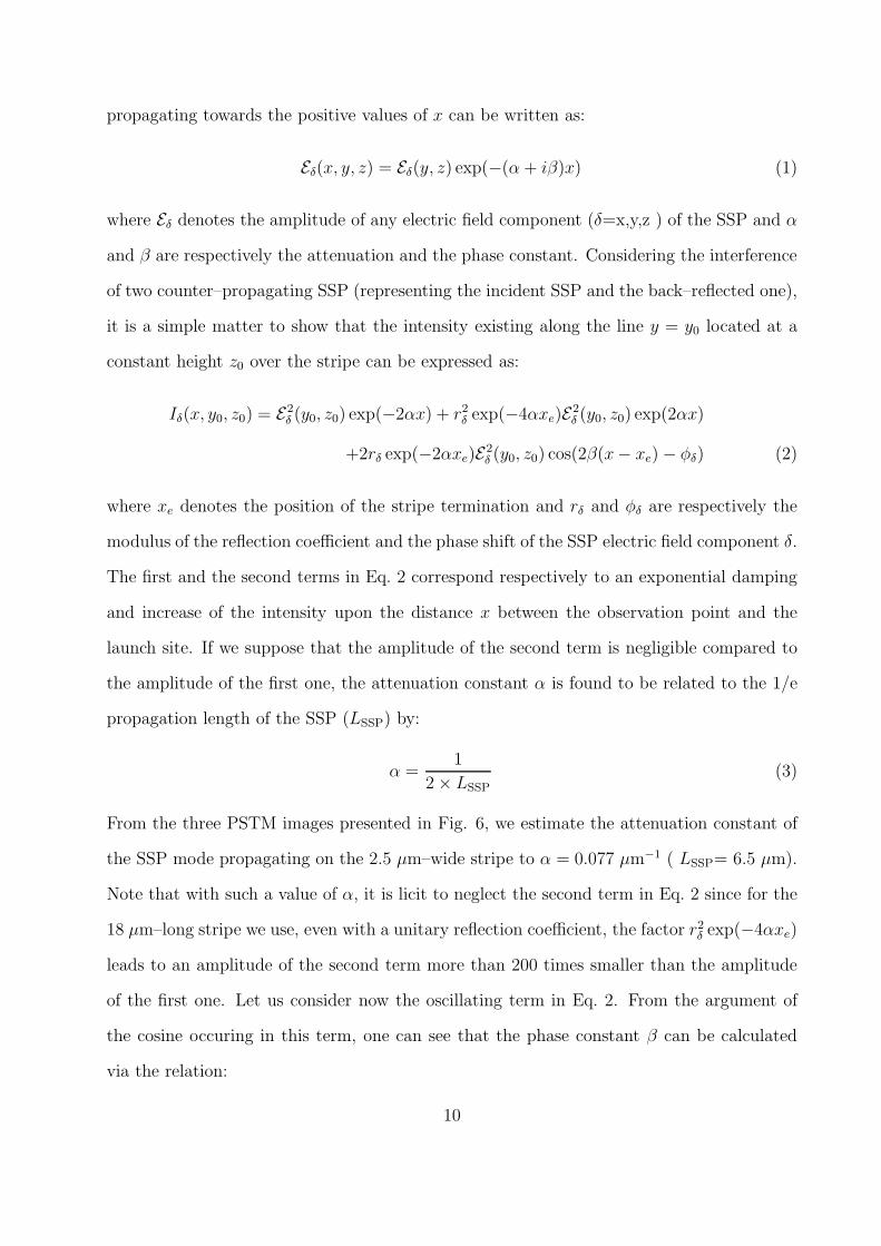
propagating towards the positive values of x can be written as:
Eδ(x, y, z) = Eδ(y, z) exp(−(α + iβ)x) (1)
where Eδ denotes the amplitude of any electric field component (δ=x,y,z ) of the SSP and α
and β are respectively the attenuation and the phase constant. Considering the interference
of two counter–propagating SSP (representing the incident SSP and the back–reflected one),
it is a simple matter to show that the intensity existing along the line y = y0 located at a
constant height z0 over the stripe can be expressed as:
Iδ(x, y0, z0) = E2δ (y0, z0) exp(−2αx) + r2
δ exp(−4αxe)E2δ (y0, z0) exp(2αx)
+2rδ exp(−2αxe)E2δ (y0, z0) cos(2β(x− xe) − φδ) (2)
where xe denotes the position of the stripe termination and rδ and φδ are respectively the
modulus of the reflection coefficient and the phase shift of the SSP electric field component δ.
The first and the second terms in Eq. 2 correspond respectively to an exponential damping
and increase of the intensity upon the distance x between the observation point and the
launch site. If we suppose that the amplitude of the second term is negligible compared to
the amplitude of the first one, the attenuation constant α is found to be related to the 1/e
propagation length of the SSP (LSSP) by:
α =1
2 × LSSP(3)
From the three PSTM images presented in Fig. 6, we estimate the attenuation constant of
the SSP mode propagating on the 2.5 µm–wide stripe to α = 0.077 µm−1 ( LSSP= 6.5 µm).
Note that with such a value of α, it is licit to neglect the second term in Eq. 2 since for the
18 µm–long stripe we use, even with a unitary reflection coefficient, the factor r2δ exp(−4αxe)
leads to an amplitude of the second term more than 200 times smaller than the amplitude
of the first one. Let us consider now the oscillating term in Eq. 2. From the argument of
the cosine occuring in this term, one can see that the phase constant β can be calculated
via the relation:
10
β =π
dSSP
(4)
if dSSP denotes the periodicity of the interference pattern observed on the PSTM images.
By averaging 20 periods on the cross–cut displays in Fig. 7b, we find a periodicity dSSP=308
nm corresponding to a phase constant β = 10.2 µm−1. The most surprising feature of
the image shown in Fig. 6c is probably the visibilty of the interference pattern over a
distance about tree times larger than the propagation length LSSP. However, this behavior
is in agreement with Eq. 2 since the amplitude of the oscillating term does not depend
on the propagation distance x. Therefore, as it can observed in Fig. 7b, the amplitude
of the stationary wave pattern remains constant along the stripe. The large amplitude of
the interferences compared to the monotonically attenuated intensity background suggests
a quite large reflection coefficient at the end of the stripe in qualitative agreement with
numerical computations of the SPP scattering by a 1D indentation in a homogeneous thin
film [17,18].
The previous experiment demonstrates that the propagation constant of a SSP can be
deduced directly from the constant height PSTM images. In order to evaluate the dispersion
of the complex propagation constant with respect to the width of the stripe, we analyse now
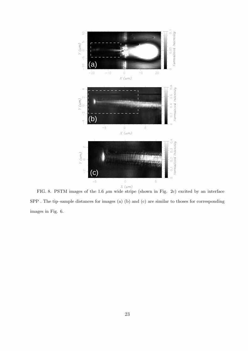
the results obtained for a stripe with a width of 1.6 µm ( length kept at 18 µm, see Fig. 2c).
The PSTM images of this new sample are shown in Fig. 8. As in the previous case, the SSP
excitation revealed by the detection of an optical near–field signal over the stripe can be
observed in the large scanning image (Fig. 8a). However, the intensity of the scattering spot
at the termination of the stripe is found to be much weaker than in the previous situation.
Note that it is licit to compare the relative intensity in Fig. 6a and 8a since in both case,
the normalization intensity is imposed by the incident spot. When reducing the scanning
area and the tip-sample distance, we observe a spatial distribution of the near–field signal
confined to the width of the stripe together with an intense spot at its termination (Figs.
8b and 8c). Since this spot is only clearly visible on the near–field images taken with a tip–
sample distance of a few tens of nanometers, we conclude that, the field at the end of the
11
stripe is mostly evanescent. Therefore, unlike what has been observed on the 2.5 µm wide
stripe (see Figs. 6a and 6b), only a small amount of the field is scattered toward the vacuum
when the SSP mode reaches the end of the stripe. A quite similar behavior has already been
mentioned for surface defect supporting a localized surface plasmon resonance at a given
frequency and exhibiting at the same frequency a small value of the vacuum scattering cross–
section [19]. The fuzzy, low contrast, surface–wave interference pattern visible in Fig. 8b
and 8c is unfortunatly to weak to allow an accurate measurement of the pattern periodicity.
However, from these images, we find a propagation length LSSP=4.8 µm significantly smaller
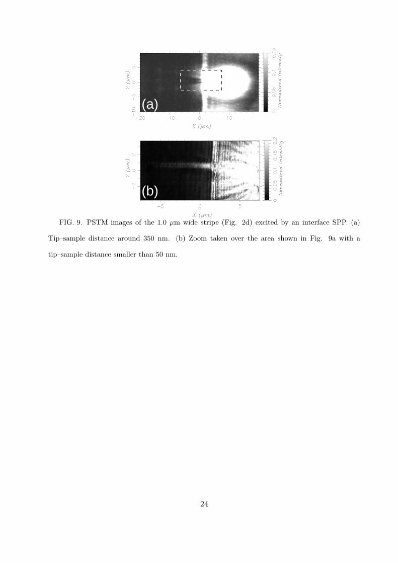
than in the previous case (α= 0.1 µm−1). The same experiments has been performed on a
stripe with a width of 1 µm. The PSTM images obtained on this sample (Figs. 9a and 9b)
comfirm that the excitation of a SSP is less efficient to propagate light as the width of the
stripe decreases. As shown in Fig. 9b, the intensity on the stripe is strongly damped with
the distance to the thin film edge. In this case, the attenation constant is about six time
larger (LSSP=1.2 µm, α= 0.42 µm−1) than for the 2.5 µm wide stripe. Obviously, with such
an attenuation, the amplitude of the SSP field at the termination of the stripe is so weak
that no scattering spot or back–reflection can be observed in the PSTM images.
With the real part of dielectric function of silver taken equal to ǫ′
Ag = −15.86 [20], the
wavelength of the SPP at an infinite silver-air interface is found to be λSPP=613 nm for
an incident wavelength of 633 nm in vacuum. Therefore, the results obtained on the 2.5
µm wide stripe suggest that if the width of the stripe is about four times λSPP the mode
excited by the SPP and propagating on the stripe exibits characterictics close to those of
the interface SPP itself. Indeed, the propagation length on this stripe is of the same order
than the one estimated on the homogeneous thin film and furthermore the wavelength of the
SSP mode (λSSP= 616 nm) is found to be almost equal to the wavelength of the interface
surface plasmon (λSPP=613 nm). If the width of the stripe is divided by two, the damping
of the SSP mode becomes so large that the propagation of light at a scale of a few microns
is not achievable anymore. On the basis of these results, we conclude that the excitation
conditions of a “wide” (within the range given above) stripe are very close to the ones of a
12

thin film SPP.
V. FOCUSING STRIPE SURFACE PLASMON MODES FIELD
The short propagation length of the SSP modes at visible frequencies prohibits the use
of the thin metal stripe for macroscopic integrated optic purposes. However, the thin metal
stripe provides an interface between a macroscopic source of illumination (the focused beam
in our case) and objects deposited on a transparent substrate or even directly on the stripe.
Accordingly, one can anticipate potential applications of the metal stripes to achieve the
optical addressing at micron scale by a surface–wave of nanoscopic objects such as metal
nanoparticles or molecules. With this goal in mind, the main challenge is the control of the
SSP mode confinement. The previous results prove that the utilization of narrow stripes to
achieve a good SSP confinement is not convenient since it leads at the same time to a drastic
reduction of the propagation length. Recently, it has been reported in several works that 2D-
waves optical components relying on elastic multiple SPP scattering could be generated from
an arrangement of large thin film indentations [4,5]. Obviously, a surface–wave lens would be
of great help to perform the focusing of the SSP mode. Unfortunatly, a lens generated from
indentations in the stripe seems rather inconceivable in our case since it would prevent SSP
propagation. To overcome these difficulties, we have adopted the most basic solution that
consists in using a “wide” stripe to keep the propagation length at a reasonable level and to
structure the shape of the stripe termination in order to squeeze the lateral extension of the
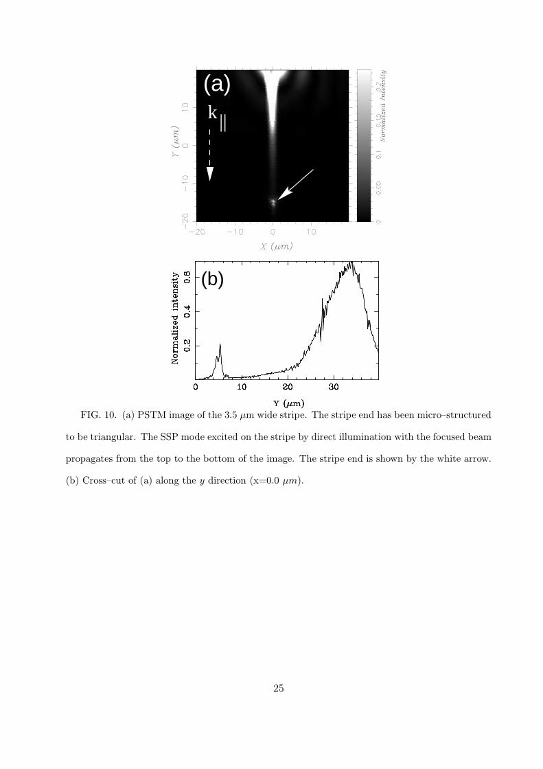
SSP mode. To this aim, a 3.5 µm wide silver stripe with a triangularly shaped termination
has been micro–fabricated. Since we known from the previous results that with such a width
the SSP launching is effective for illuminations parameters close to those that correspond to
the excitation of an infinite thin film SPP, the stripe has been excited with the focused beam
shining directly on it at an angle of incidence of 43o. The constant height PSTM image shown
in Fig. 10a has been obtained for an incident spot located about 30 µm from the stripe end.
The SSP propagation (from the top to the bottom) is clearly visible and leads to an intense
13
scattering spot at the stripe termination. From the cross–cut displayed in Fig. 10b, we find
a propagation length LSSP =7.0 µm close to the one previously measured for the 2.5 µm
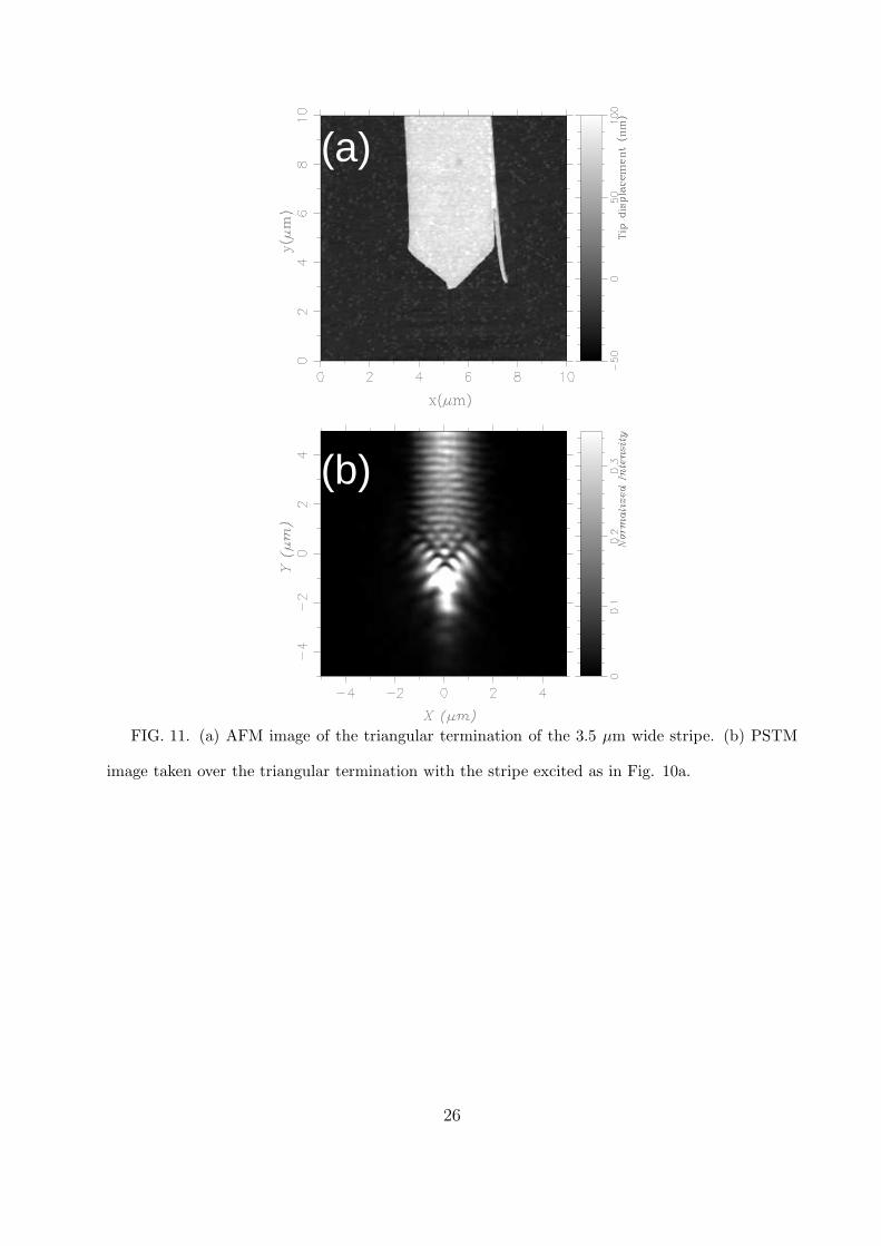
wide stripe. To probe the behavior of the SSP when encountering the stripe end (Fig. 11a),
a PSTM image has been taken over a reduced scanning area (Fig. 11b). Far from the stripe
end, we notice a standing wave pattern of the same kind than the one previously observed
in Fig. 6c. By direct comparison with the AFM image of the stripe, the confinement of the
SSP mode appears unambiguously. As shown in Fig. 11a, the stripe end is represented by
a triangle with an opening angle of about 90o. On the right side of the stripe, a narrow
silver wire resulting from a defect of the lithographic process can be observed. It turns out
that this wire does not pertub significantly the SSP field. Within the triangular area, the
PSTM image exhibits a two–dimensionnal interference pattern attributed to the interaction
of the incident SSP with the two SSP reflected by each side of the triangle. At the very
end of the stripe, we observe an intense localized spot due to foward scattering of the SSP
presenting a lateral extension of less than one third of the stripe width (FWHM=1.0 µm in
the x direction). Since in the case of a rectangular stripe termination the scattering spot
extends over the entire width of the stripe (see Figs. 6c and 8c), we conclude that, by using
a triangular termination, we have achieved the focusing of the SSP field.
VI. CONCLUSION
In summary, we have used a PSTM set–up to demonstrate the feasibility of surface
plasmon guiding by laterally confined thin films deposited on a glass substrate. To excite
the SSP modes sustained by the stripes, we first use a SPP launched by a focused beam on
a homogeneous thin film area whose lateral extension is much larger than the incident spot.
If the width of the stripe is about four times the SPP wavelength, the propagation constant
of the SSP mode is found to be close to the one of the SPP. Therefore, for stripe widths
down to 2.5 µm stripes, a good coupling between thin film SPP and the stripe modes can be
achieved at visible frequencies. Once launched, the SSP mode is damped with propagation
14

distance but, laterally, remains well confined all along the stripe. When reaching the stripe
end, a quite large back–reflection of the SSP field leads to the creation of a stationary wave
pattern exhibiting a constant amplitude all along the stripe. Finally, a direct excitation
of the SSP mode by the incident focused beam has been demonstrated for a 3.5 µm wide
stripe. Using a triangularly shaped stripe termination, we have shown that a focusing of
the SSP field could be achieved. On the basis of these results, many other situations as the
splitting or the deviation of SSP can be considered. Experiments dealing with these topics
are in progress and will be reported elsewhere.
15
REFERENCES
[1] H. Raether, Surface Plasmons, Springer Tracts in Modern Physics, Vol 111 (Springer,
Berlin, 1988).
[2] R.C. Reddick, R.J. Warmack, T.L. Ferrell, Phys. Rev. B, 39, 767 (1989).
[3] P. Dawson, F. de Fornel, J.P. Goudonnet, Phys. Rev. Lett., 72, 2927 (1994).
[4] S. I. Bozhevolnyi, F. A. Pudonin, Phys. Rev. Lett., 78, 2823 (1997).
[5] S. I. Bozhevolnyi, V. Coello, Phys. Rev. B, 58, 10899 (1998).
[6] I. I. Smolyaninov, D. L. Mazzoni, C. C. Davis, Phys. Rev. Lett., 77, 3877 (1996).
[7] P. Berini, Phys. Rev. B, 61, 10484 (2000).
[8] R. Charbonneau, P. Berini, E. Berolo, E. Lisicka-Shrzek, Optics Lett. 25, 844 (2000).
[9] P. Berini, Optics Express, 7, 329 (2000).
[10] E. Devaux, A. Dereux, E. Bourillot, J-C Weeber, Y. Lacroute, J-P Goudonnet, Ch.
Girard, Phys. Rev. B, 62, 10504 (2000).
[11] J. R. Krenn, A. Dereux, J-C Weeber, E. Bourillot, Y. Lacroute, J-P Goudonnet, G.
Schider, W. Gotschy, A. Leitner, F. R. Ausseneg, Ch. Girard, Phys. Rev. Lett., 82,
2590 (1999).
[12] J-C Weeber, E. Bourillot, A. Dereux, J-P Goudonnet, Y. Chen, Ch. Girard, Phys. Rev.
Lett., 77, 5332 (1996).
[13] M. van Exter, A. Lagendijk, Phys. Rev. Lett., 60, 49 (1988).
[14] R. F. Wallis, A. A. Maradudin, G. I. Stegeman, Appl. Phys. Lett. 42, 764 (1983).
[15] H. A. Jamid, S. J. Al-Bader, IEEE Photonic Technology Letter, 7, 321 (1995).
[16] H. A. Jamid, S. J. Al-Bader, IEEE Photonic Technology Letter, 9, 220 (1997).
16

[17] J. A. Sanchez-Gil, Appl. Phys. Lett., 73, 3509 (1998).
[18] U. Schroeter, S. Seider, S. Tode, D. Heitmann, Ultramicroscopy, 68, 223 (1997).
[19] A. V. Shchegrov, I. V. Novikov, A. A. Maradudin, Phys. Rev. Lett., 78, 4269 (1997).
[20] Handbook of Optical Constants of Solids, edited by D. Palik (Academic, New York,
1985).
17
FIGURES
elec
trod
eZ
LASER
PM I/VPC
Prism Microscope objective
Polarizer
Focusing lens
Optical fiber
FeedbackFiber tip
PSTM
STM
V offset
Z voltage
Sample
Z voltage
FIG. 1. Schematic view of the experimental PSTM setup. (PM): Photomultiplier, (I/V): Cur-
rent/voltage amplifier, (details see text).
µ250 m
(a)(d)
(c)(b)
(b)(d)
(c)
FIG. 2. (a) SEM image of the silver sample designed to study the coupling between interface
SPP and the modes sustained by finite width thin metal films (stripes). Several stripes of different
widths are connected to a large homogeneous thin film area of 250×250 µm2. Atomic force micro-
scope images of the three stripes considered. (b) width=2.5 µm. (c) width=1.6 µm. (d) width=1.0
µm
18
(c)
(a)
(b)
FIG. 3. PSTM image of the incident spot for an angle of incidence of 43o. (a) The beam is
focused on the surface of the ITO doped glass substrate. (b) The spot has been moved on the
homogeneous silver thin film area. The dashed line marks the thin film edge. (c) Cross–cut of (b)
along the dotted line. The assymetric shape of the spot is due to the propagation of the SPP along
the silver–air interface. Inelastic SPP scattering leads to an enhanced optical signal over the film
edge (black arrow).
19
(a)
(b)
FIG. 4. PSTM image of the 2.5 µm wide stripe excited by a SPP launched on the homogeneous
thin film area. (a) The incident spot is located in front of the stripe. At the end of the stripe
a scattering spot (white arrow) is visible. (b) The incident spot has been moved 15 µm in the y
direction. The scanning area is the same than that of (a).
FIG. 5. PSTM image of the 2.5 µm wide stripe when the plane of incidence is rotated 45o
with respect to the long axis of the stripe (the surface projection of the film edges and the stripe
correspond to the white dashed lines).
20
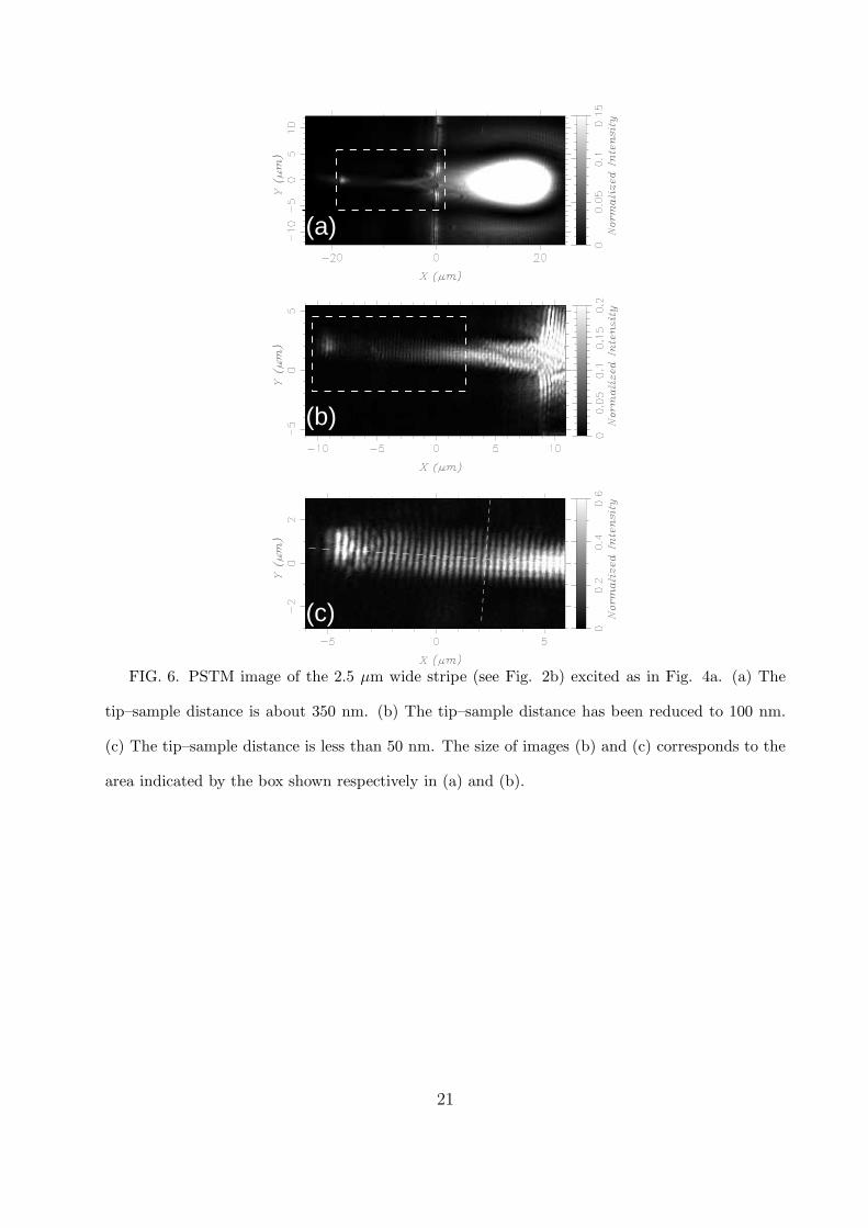
(b)
(c)
(a)
FIG. 6. PSTM image of the 2.5 µm wide stripe (see Fig. 2b) excited as in Fig. 4a. (a) The
tip–sample distance is about 350 nm. (b) The tip–sample distance has been reduced to 100 nm.
(c) The tip–sample distance is less than 50 nm. The size of images (b) and (c) corresponds to the
area indicated by the box shown respectively in (a) and (b).
21
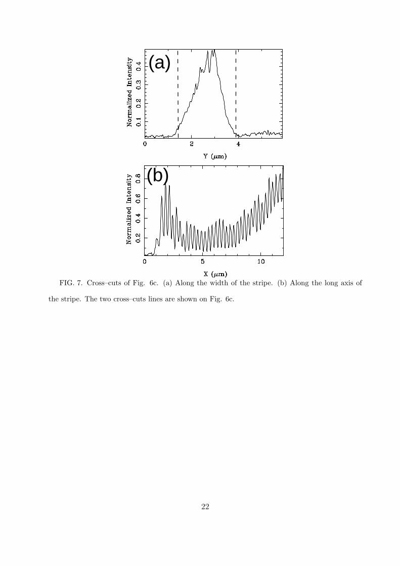
(b)
(a)
FIG. 7. Cross–cuts of Fig. 6c. (a) Along the width of the stripe. (b) Along the long axis of
the stripe. The two cross–cuts lines are shown on Fig. 6c.
22
(b)
(a)
(c)
FIG. 8. PSTM images of the 1.6 µm wide stripe (shown in Fig. 2c) excited by an interface
SPP . The tip–sample distances for images (a) (b) and (c) are similar to thoses for corresponding
images in Fig. 6.
23
(b)
(a)
FIG. 9. PSTM images of the 1.0 µm wide stripe (Fig. 2d) excited by an interface SPP. (a)
Tip–sample distance around 350 nm. (b) Zoom taken over the area shown in Fig. 9a with a
tip–sample distance smaller than 50 nm.
24
k||
(a)
(b)
FIG. 10. (a) PSTM image of the 3.5 µm wide stripe. The stripe end has been micro–structured
to be triangular. The SSP mode excited on the stripe by direct illumination with the focused beam
propagates from the top to the bottom of the image. The stripe end is shown by the white arrow.
(b) Cross–cut of (a) along the y direction (x=0.0 µm).
25
(b)
(a)
FIG. 11. (a) AFM image of the triangular termination of the 3.5 µm wide stripe. (b) PSTM
image taken over the triangular termination with the stripe excited as in Fig. 10a.
26