Embed Size (px)
Citation preview
Costanza, May 7-8, 2013 M. Balucani
New selective processing technique for solar cell
M. Balucani1,4, K. Kholostov1, P. Nenzi1, R. Crescenzi1,
L. Serenelli2, M. Izzi2, M. Tucci2
D. Bernardi3
D. Ciarniello4
1 DIET-Sapienza University of Rome, Via Eudossiana, 18 - 00184 Roma (ITALY),; 2 ENEA Casaccia Research Centre Rome, ITALY,
3 2BG S.r.l. Padova (ITALY), 4 Rise TechnolgyS.r.l. Roma (ITALY),
2
Costanza, May 7-8, 2013 M. Balucani
Outline
•Introduction
•Plating Technology Key Issues
•What we are able to solve and how we do it
•Dynamic Liquid Drop/Meniscus
•Main results achieved
•Conclusions
3
Costanza, May 7-8, 2013 M. Balucani
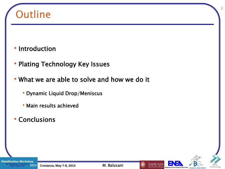
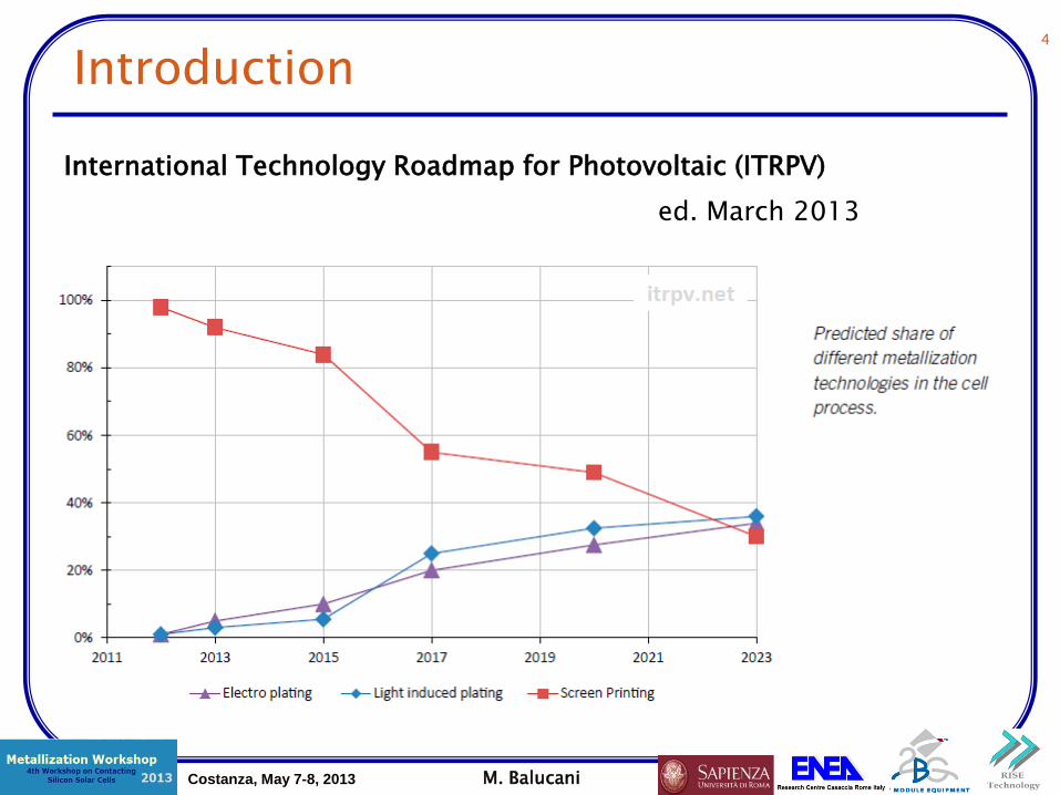
International Technology Roadmap for Photovoltaic (ITRPV)
ed. March 2013
Introduction
4
Costanza, May 7-8, 2013 M. Balucani
International Technology Roadmap for Photovoltaic (ITRPV)
ed. March 2013
Introduction

5
Costanza, May 7-8, 2013 M. Balucani
Current plating main key issues:
Pin-holes Front side: Ni-Cu adhesion to Si Back side: direct plating on Al Speed of Plating Throughput and Space floor Drag-out Reduce additive consumption
Plating Technology Key Issues Before the introduction of alternative metallization techniques, technical issues
in reliability and adhesion have to be solved. Appropriate equipment also needs to be available (ITRPV)
LIP 0.6-3.0 A/dm2
0.3-0.5 ml/w
6
Costanza, May 7-8, 2013 M. Balucani
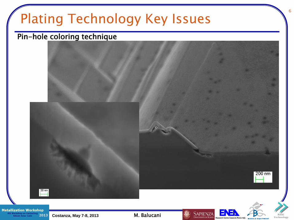
Pin-hole coloring technique
Plating Technology Key Issues
7
Costanza, May 7-8, 2013 M. Balucani
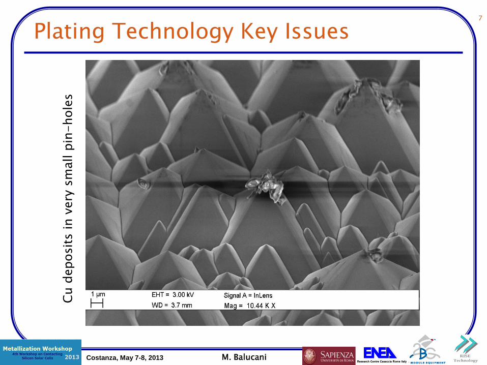
Cu d
eposit
s in v
ery
sm
all p
in-hole
s
Plating Technology Key Issues
8
Costanza, May 7-8, 2013 M. Balucani
What we are able to solve…..
Pin-holes Localized Treatment Front side:Ni-Cu adhesion to Si Porous Silicon Back side: direct plating on Al Yes …. Speed of Plating Jet plating : Vfluid=2ms-1
Drag-out Very low...................
9
Costanza, May 7-8, 2013 M. Balucani
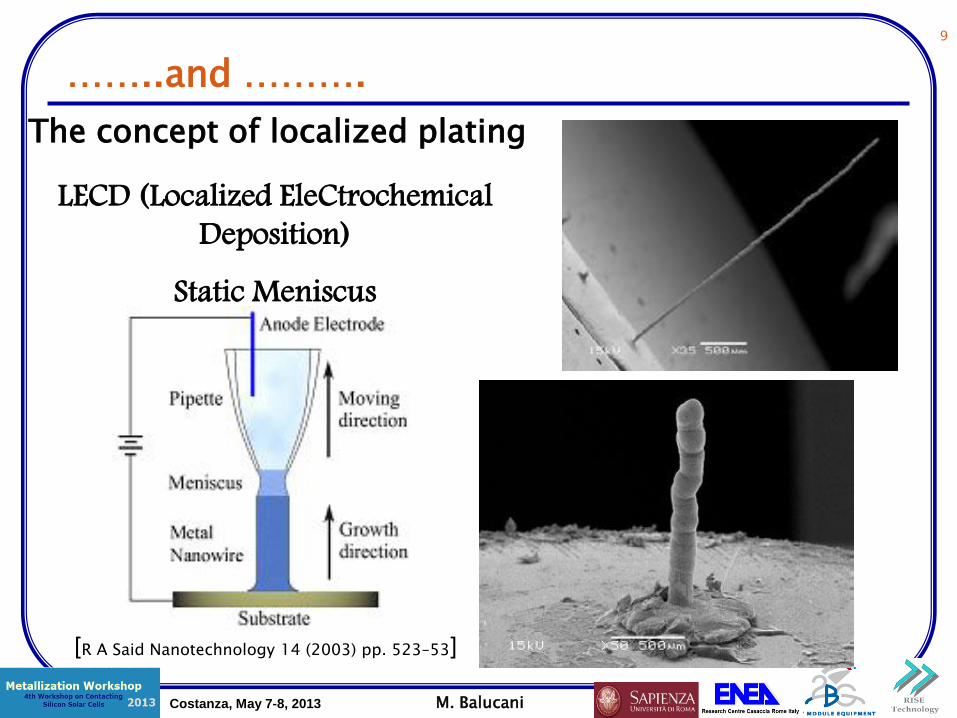
……..and ……….
The concept of localized plating
LECD (Localized EleCtrochemical
Deposition)
Static Meniscus
[R A Said Nanotechnology 14 (2003) pp. 523–53]
10
Costanza, May 7-8, 2013 M. Balucani
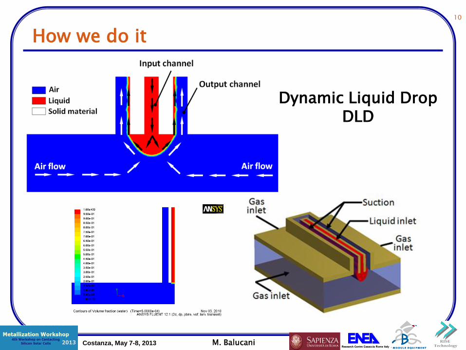
How we do it
Dynamic Liquid Drop DLD
11
Costanza, May 7-8, 2013 M. Balucani
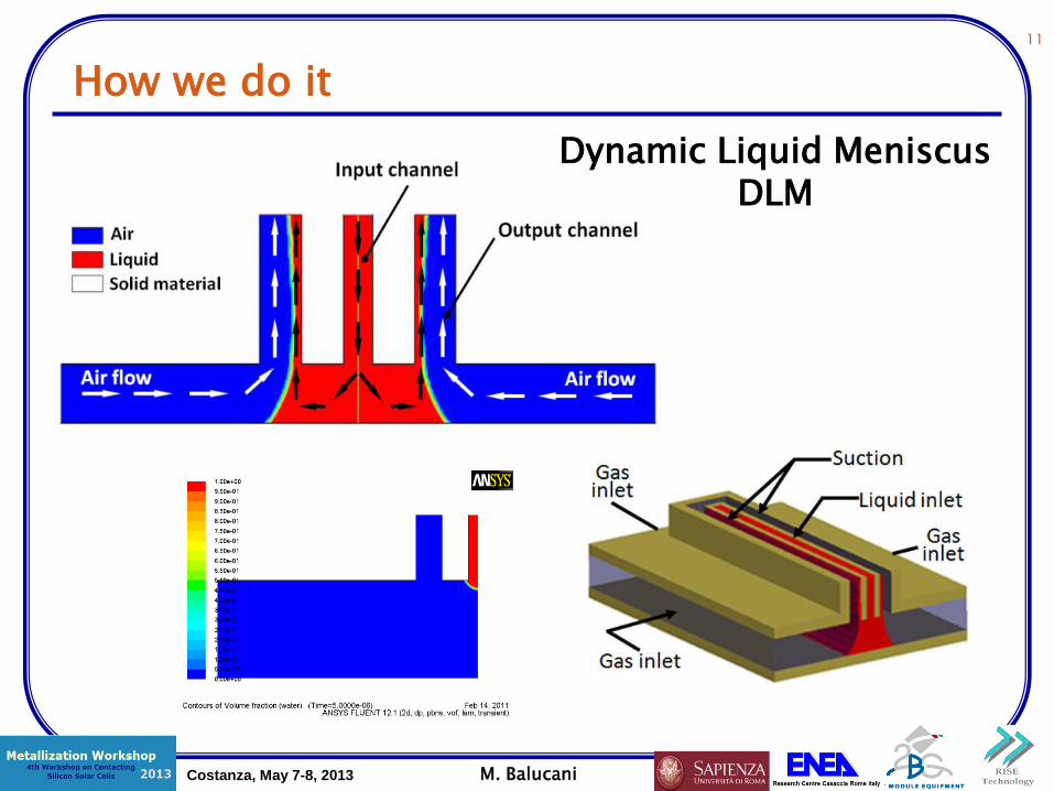
How we do it
Dynamic Liquid Meniscus DLM
12
Costanza, May 7-8, 2013 M. Balucani
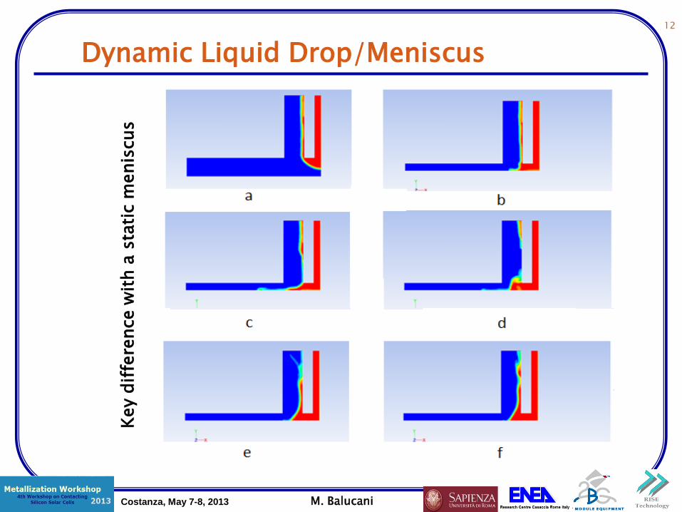
Dynamic Liquid Drop/Meniscus
Key d
iffe
rence w
ith a
sta
tic m
enis
cus
13
Costanza, May 7-8, 2013 M. Balucani
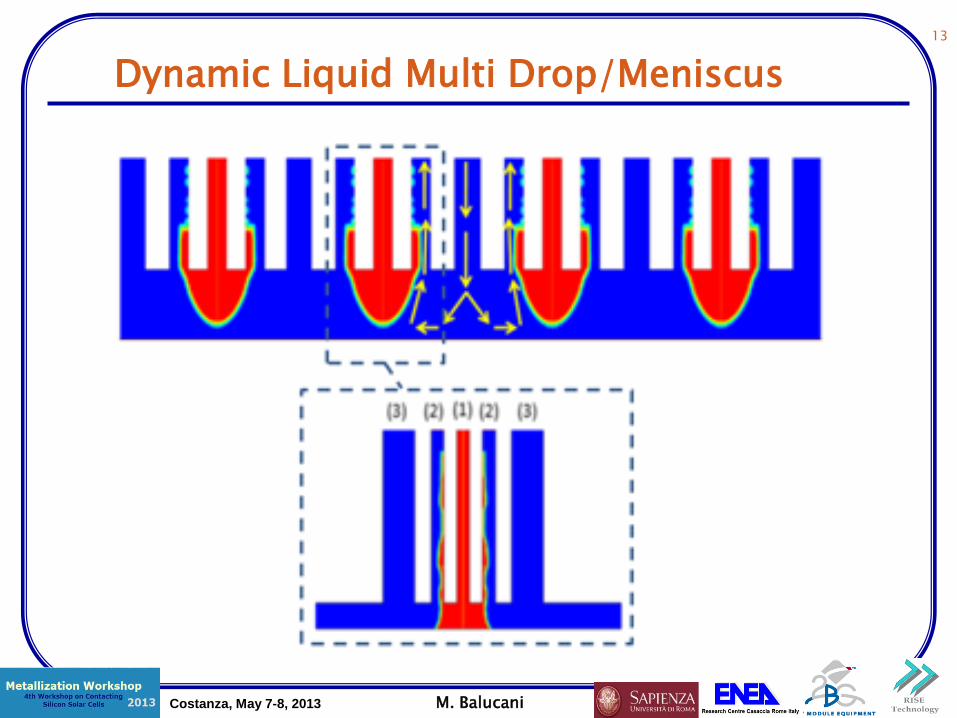
Dynamic Liquid Multi Drop/Meniscus

14
Costanza, May 7-8, 2013 M. Balucani
Dynamic Liquid Drop/Meniscus
Gravity influence
Inlet > 8 mm Go Up-side down
15
Costanza, May 7-8, 2013 M. Balucani
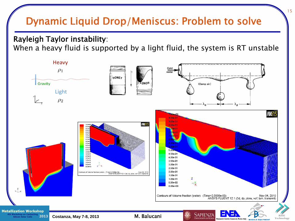
Rayleigh Taylor instability: When a heavy fluid is supported by a light fluid, the system is RT unstable
Dynamic Liquid Drop/Meniscus: Problem to solve
16
Costanza, May 7-8, 2013 M. Balucani
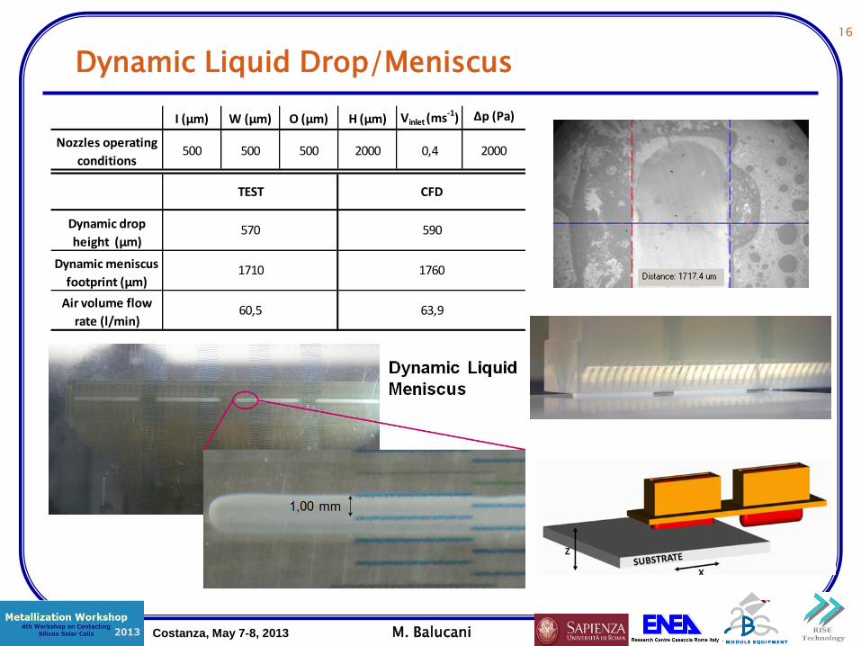
I (µm) W (µm) O (µm) H (µm) Vinlet (ms-1) Δp (Pa)
500 500 500 2000 0,4 2000Nozzles operating
conditions
TEST CFD
60,5 63,9Air volume flow
rate (l/min)
Dynamic drop
height (µm)
Dynamic meniscus
footprint (µm)
570 590
1710 1760
Dynamic Liquid Drop/Meniscus
17
Costanza, May 7-8, 2013 M. Balucani
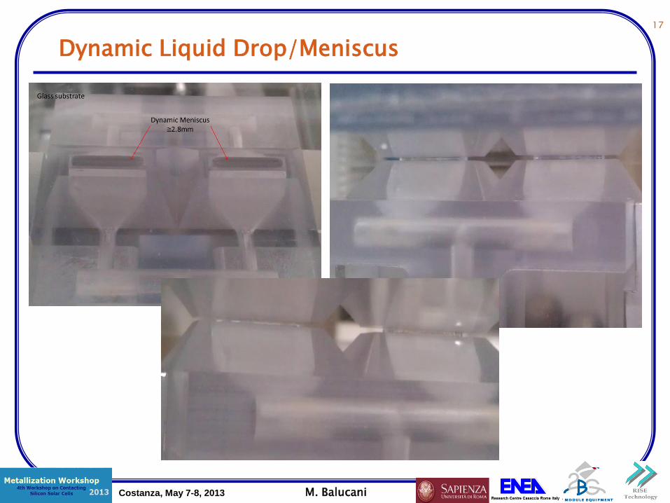
Dynamic Liquid Drop/Meniscus
18
Costanza, May 7-8, 2013 M. Balucani
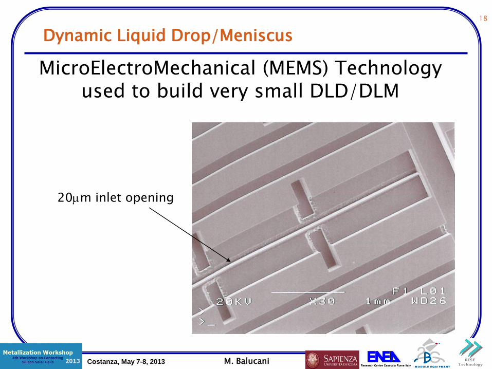
Dynamic Liquid Drop/Meniscus
20m inlet opening
MicroElectroMechanical (MEMS) Technology used to build very small DLD/DLM

19
Costanza, May 7-8, 2013 M. Balucani
Dynamic Liquid Drop/Meniscus: how we use it
DLD-DLM configurations for: a) Opening of ARC layer or any kind of etching
b) Porous Silicon formation on n-type doped emitter
c) Electroplating on Porous Silicon region on n-type doped emitter
d) Porous Silicon suitable for n- or p-type doped emitter
e) Electroplating on Porous Silicon region on p-type emitter
20
Costanza, May 7-8, 2013 M. Balucani
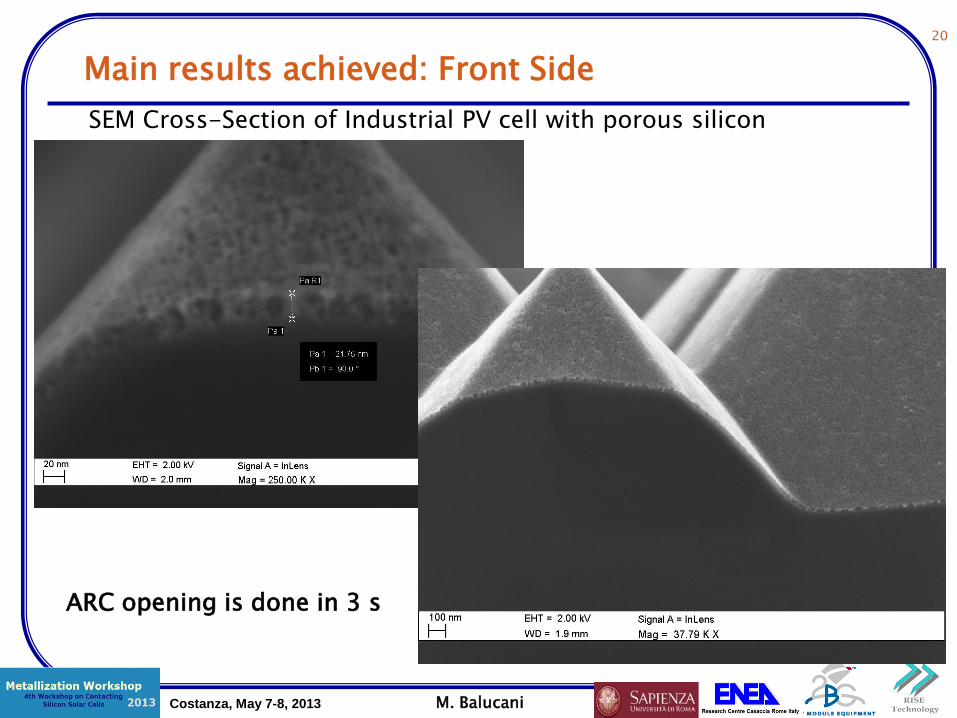
Main results achieved: Front Side
SEM Cross-Section of Industrial PV cell with porous silicon
ARC opening is done in 3 s
21
Costanza, May 7-8, 2013 M. Balucani
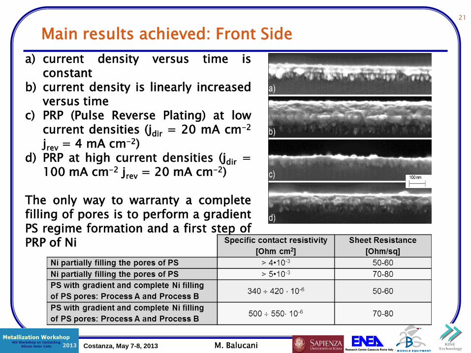
Main results achieved: Front Side
a) current density versus time is constant
b) current density is linearly increased versus time
c) PRP (Pulse Reverse Plating) at low current densities (jdir = 20 mA cm-2 jrev = 4 mA cm-2)
d) PRP at high current densities (jdir = 100 mA cm-2 jrev = 20 mA cm-2)
The only way to warranty a complete filling of pores is to perform a gradient PS regime formation and a first step of PRP of Ni
22
Costanza, May 7-8, 2013 M. Balucani
Main results achieved: Front Side

23
Costanza, May 7-8, 2013 M. Balucani
Main results achieved: Front Side
Cross-section made by Focus Ion Beam
Cu
Ni
Si
24
Costanza, May 7-8, 2013 M. Balucani
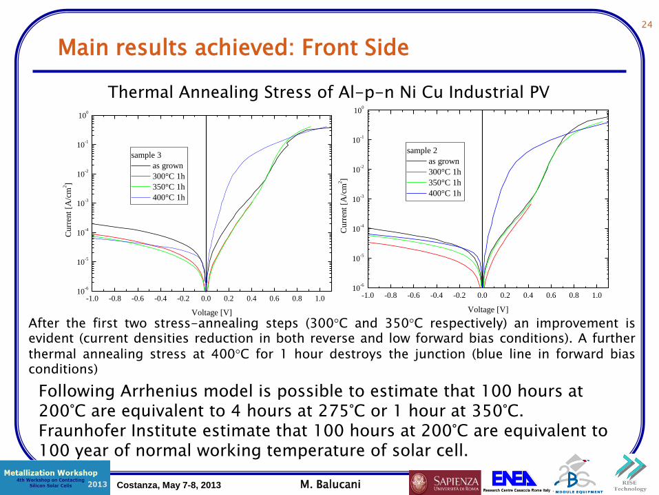
Main results achieved: Front Side
Thermal Annealing Stress of Al-p-n Ni Cu Industrial PV
-1.0 -0.8 -0.6 -0.4 -0.2 0.0 0.2 0.4 0.6 0.8 1.010
-6
10-5
10-4
10-3
10-2
10-1
100
Cu
rren
t [A
/cm
2]
Voltage [V]
sample 3
as grown
300°C 1h
350°C 1h
400°C 1h
-1.0 -0.8 -0.6 -0.4 -0.2 0.0 0.2 0.4 0.6 0.8 1.010
-6
10-5
10-4
10-3
10-2
10-1
100
Cu
rren
t [A
/cm
2]
Voltage [V]
sample 2
as grown
300°C 1h
350°C 1h
400°C 1h
Following Arrhenius model is possible to estimate that 100 hours at 200°C are equivalent to 4 hours at 275°C or 1 hour at 350°C. Fraunhofer Institute estimate that 100 hours at 200°C are equivalent to 100 year of normal working temperature of solar cell.
After the first two stress-annealing steps (300°C and 350°C respectively) an improvement is evident (current densities reduction in both reverse and low forward bias conditions). A further thermal annealing stress at 400°C for 1 hour destroys the junction (blue line in forward bias conditions)

25
Costanza, May 7-8, 2013 M. Balucani
Main results achieved: Back Side
Force [N]
Deformation [mm]
Silv
er
paste
adhesio
n t
est
F=0.5N/mm
26
Costanza, May 7-8, 2013 M. Balucani
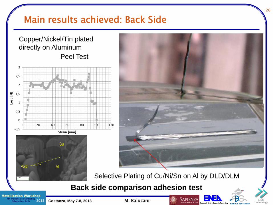
Back side comparison adhesion test
Copper/Nickel/Tin plated
directly on Aluminum
Selective Plating of Cu/Ni/Sn on Al by DLD/DLM
Peel Test
Main results achieved: Back Side
27
Costanza, May 7-8, 2013 M. Balucani
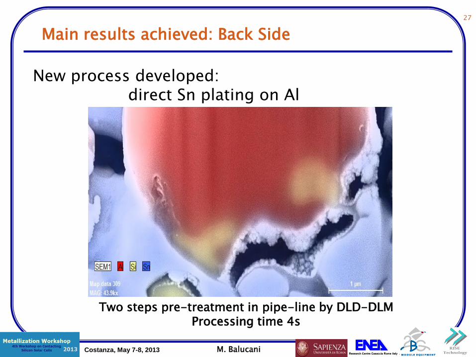
Main results achieved: Back Side
New process developed: direct Sn plating on Al
Two steps pre-treatment in pipe-line by DLD-DLM Processing time 4s
28
Costanza, May 7-8, 2013 M. Balucani
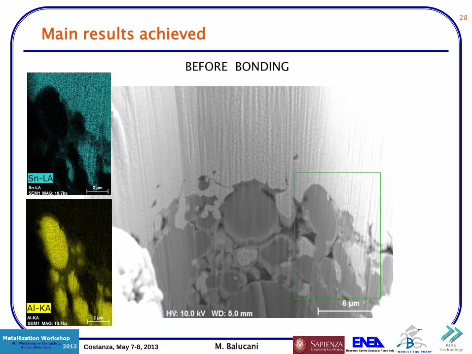
BEFORE BONDING
Main results achieved

29
Costanza, May 7-8, 2013 M. Balucani
AFTER BONDING AND PEEL TEST: ADHESION >1.0 N/mm
Main results achieved
Different solar cell 4x4cm2 with back Ag localized contact were compared with Sn localized contact and direct Al contact
Sample Voc [mV] Jsc [mAcm-2] Normalized FF Normalized Eff Rs [cm2]
S29 - Al contact 625 36.3 1 1.000 2.3 S29 - Ag contact 586 34,6 0.782 0.700 3.0 S29 - Sn contact 624 36.1 0.992 0.992 2.3
S30 - Al contact 628 35.4 1 1.000 2.9 S30 - Ag contact 590 34.5 0.825 0.756 3.0 S30 - Sn contact 628 34.7 0.998 0.980 2.8
30
Costanza, May 7-8, 2013 M. Balucani
Conclusions
The New Selective Wet Processing allows:
• Plating on back contact solar cell (no need of resit)
• Plating on front contact (no need of resit)
Very fast process: Jet Plating Vfluid=2ms-1
Drag-out is very low……
• What more can DLD-DLM offer: • Edge isolation of solar cell • Wet etching (e.g. texturization of solar cells)
• And ……many other applications
Costanza, May 7-8, 2013 M. Balucani
Thanks for your attention
M. Balucani1,4, K. Kholostov1, P. Nenzi1, R. Crescenzi1,
L. Serenelli2, M. Izzi2, M. Tucci2
D. Bernardi3
D. Ciarniello4
1 DIET-Sapienza University of Rome, Via Eudossiana, 18 - 00184 Roma (ITALY),; 2 ENEA Casaccia Research Centre Rome, ITALY,
3 2BG S.r.l. Padova (ITALY), 4 Rise TechnolgyS.r.l. Roma (ITALY),