Embed Size (px)
Citation preview
1
NISC Modeling and Compilation
Mehrdad Reshadi and Daniel Gajski
Center for Embedded Computer Systems University of California, Irvine Irvine, CA 92697-3425, USA
(949) 824-8059
{reshadi, gajski}@cecs.uci.edu
CECS Technical Report 04-33 December, 2004
2
NISC Modeling and Compilation
Mehrdad Reshadi, Daniel Gajski
Center for Embedded Computer Systems University of California, Irvine Irvine, CA 92697-3425, USA
(949) 824-8059
{reshadi, gajski}@cecs.uci.edu
CECS Technical Report 04-33 December, 2004
Abstract Running an application on a general purpose processor is not very efficient and implementing the whole application in hardware is not always possible. The best option is to run the application on a customized datapath that is designed based on the characteristics of the application. The instruction set interface in normal processors limits the possible customization of the datapath. In NISC, the instruction interface is removed and the datapath is directly controlled. Therefore, any customization in the datapath can be easily utilized by the supporting tools such as compiler and simulator and one set of such tools is enough to handle all kinds of datapaths. To achieve this goal, a generic model is needed to capture the datapath information that these tools require. In this report we present one such model and show how it can be used for simulation and compilation. We also explain the structure of a NISC compiler and show some preliminary experiments on multiple NISC architecture and their comparison with MIPS architecture.
i
Contents 1 Introduction ...........................................................................................................................1 2 NISC’s View of the Processor ................................................................................................2 3 NISC Methodology................................................................................................................4 4 NISC Processor Model...........................................................................................................6
4.1 Model of Datapath ........................................................................................................7 4.2 Multi-cycle and pipelined component support .............................................................10 4.3 Pipelined datapath.......................................................................................................11
5 Simulation ...........................................................................................................................11 6 Compilation .........................................................................................................................12
6.1 Compiling the input program ......................................................................................13 6.1.1 Types......................................................................................................................13 6.1.2 Global variables......................................................................................................13 6.1.3 Functions ................................................................................................................13 6.1.4 Constants ................................................................................................................14
6.2 Architecture preprocessor............................................................................................14 6.3 Pre-binder ...................................................................................................................14 1. Immediate .......................................................................................................................14 2. RegisterDirect .................................................................................................................14 3. RegisterIndex..................................................................................................................14 4. MemoryDirect.................................................................................................................14 5. MemoryIndex .................................................................................................................14 6.4 CDFG constructor.......................................................................................................15 6.5 Scheduler ....................................................................................................................15 6.6 Register binder............................................................................................................16
7 Experiments.........................................................................................................................16 8 Summary and Future work ...................................................................................................19 9 References ...........................................................................................................................20
ii
List Of Figures Figure 1 - General sequential hardware ..........................................................................................2 Figure 2 - RISC and CISC block diagram ......................................................................................3 Figure 3 - NISC block diagram ......................................................................................................4 Figure 4 - NISC methodology........................................................................................................5 Figure 5 – A sample NISC architecture ..........................................................................................6 Figure 6 - NISC model of a simple datapath...................................................................................7 Figure 7 - Component database for Figure 6...................................................................................8 Figure 8 - Pseudo code of the simulation main loop .....................................................................11 Figure 9 - Main simulation function for datapath of Figure 6........................................................12 Figure 10- NISC compiler flow Figure 4b ....................................................................................13 Figure 11- A sample SFSMD.......................................................................................................15 Figure 12- NP: NISC with no pipelining ......................................................................................17 Figure 13- CP: NISC with controller pipelining ...........................................................................17 Figure 14- CDP: NISC with controller and datapath pipelining ....................................................17 Figure 15- CDP+F: NISC with controller and datapath pipelining + data forwarding....................17 Figure 16- NM1: NISC with datapath similar to MIPS .................................................................17 Figure 17- NM2: NISC with datapath similar to MIPS but having one extra ALU ........................17
List Of Tables Table 1- Control word bit width for NISC architectures ...............................................................17 Table 2- Number of control words in NISC architectures and instructions in MIPS ......................18 Table 3- Ratio of NISC to MIPS program memory size................................................................18 Table 4- Average operation per control word in NISC architectures. ............................................18 Table 5- Compilation times (in seconds) ......................................................................................18 Table 6- Number of clock cycles..................................................................................................19 Table 7- Speedup over MIPS .......................................................................................................19
1
NISC Modeling and Compilation
Mehrdad Reshadi and Daniel Gajski Center for Embedded Computer Systems
University of California, Irvine
1 Introduction In a Soc design, the system is usually partitioned into smaller components that execute a specific set of tasks or applications. These components are usually in the form of an IP, developed by a third party or reused from previous designs. The efficiency of the SoC design relies on efficient use of IP cores as well as use of efficient IP cores. Efficient use of an IP core depends on the tools and techniques that are utilized for mapping the application to the IP. On the other hand the efficiency of an IP depends on how well it matches the needs and behavior of the application. The system components may be implemented by pure software, running on a general purpose processor; pure hardware using logic gates; or a mixture of software and customized hardware.
General purpose processors are fairly easy to program and the size of the application is bounded by the size of the program memory, which is normally very large. However, because of their generality, these processors are not very efficient in terms of quality metrics such as performance and energy consumption. Such processors use an instruction set as their interface which is used by a compiler to map the application. The available compilers can perform well as long as the instruction set is fixed, very generic and fairly simple (RISC type). In other words, the efficiency of general purpose processors and the efficient use of them are very much limited by their instruction set.
Implementing a system component in hardware only using standard cell libraries can be very efficient in terms of performance and energy consumption. However, they have very little flexibility and the size of the applications that they can implement is bounded by the available chip area. Because of the complexities involved in developing such components, the synthesis tools can work only on relatively simple applications. High design complexity and cost of these components limits their use in SoC.
A better option for implementing a system component or an IP is to have a custom hardware for each application that runs an optimized software. This approach is more efficient than using only general purpose processor and more flexible than using logic blocks. Application Specific Instruction set Processors (ASIPs) tried to achieve this goal by performing the following steps:
1. Finding a proper and critical sub-functionality of the application as a candidate for speedup.
2. Designing an efficient datapath or upgrading an existing one for executing the candidate sub-functionality.
3. Designing an instruction and upgrading the processor instruction decoder accordingly.
4. Upgrading the compiler to take advantage of the new complex instruction.
5. Compiling the application to use the new improved datapath.
Although the ASIP approach can offer higher performance for applications, it faces two major limitations:
1. Typically in ASIPs, an already existing general purpose processor (base processor) is upgraded to run the application faster. Due to the timing and area limitations that the base processor imposes on the instruction decoder, the complexity of the instructions generated in the third step in the above ASIP approach is very much limited by the instruction decoder. This in turn limits the type of possible
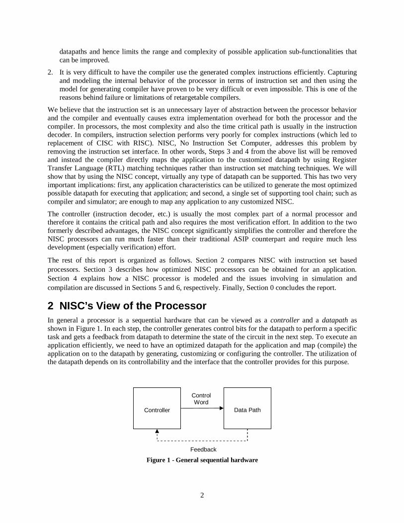
2
datapaths and hence limits the range and complexity of possible application sub-functionalities that can be improved.
2. It is very difficult to have the compiler use the generated complex instructions efficiently. Capturing and modeling the internal behavior of the processor in terms of instruction set and then using the model for generating compiler have proven to be very difficult or even impossible. This is one of the reasons behind failure or limitations of retargetable compilers.
We believe that the instruction set is an unnecessary layer of abstraction between the processor behavior and the compiler and eventually causes extra implementation overhead for both the processor and the compiler. In processors, the most complexity and also the time critical path is usually in the instruction decoder. In compilers, instruction selection performs very poorly for complex instructions (which led to replacement of CISC with RISC). NISC, No Instruction Set Computer, addresses this problem by removing the instruction set interface. In other words, Steps 3 and 4 from the above list will be removed and instead the compiler directly maps the application to the customized datapath by using Register Transfer Language (RTL) matching techniques rather than instruction set matching techniques. We will show that by using the NISC concept, virtually any type of datapath can be supported. This has two very important implications: first, any application characteristics can be utilized to generate the most optimized possible datapath for executing that application; and second, a single set of supporting tool chain; such as compiler and simulator; are enough to map any application to any customized NISC.
The controller (instruction decoder, etc.) is usually the most complex part of a normal processor and therefore it contains the critical path and also requires the most verification effort. In addition to the two formerly described advantages, the NISC concept significantly simplifies the controller and therefore the NISC processors can run much faster than their traditional ASIP counterpart and require much less development (especially verification) effort.
The rest of this report is organized as follows. Section 2 compares NISC with instruction set based processors. Section 3 describes how optimized NISC processors can be obtained for an application. Section 4 explains how a NISC processor is modeled and the issues involving in simulation and compilation are discussed in Sections 5 and 6, respectively. Finally, Section 0 concludes the report.
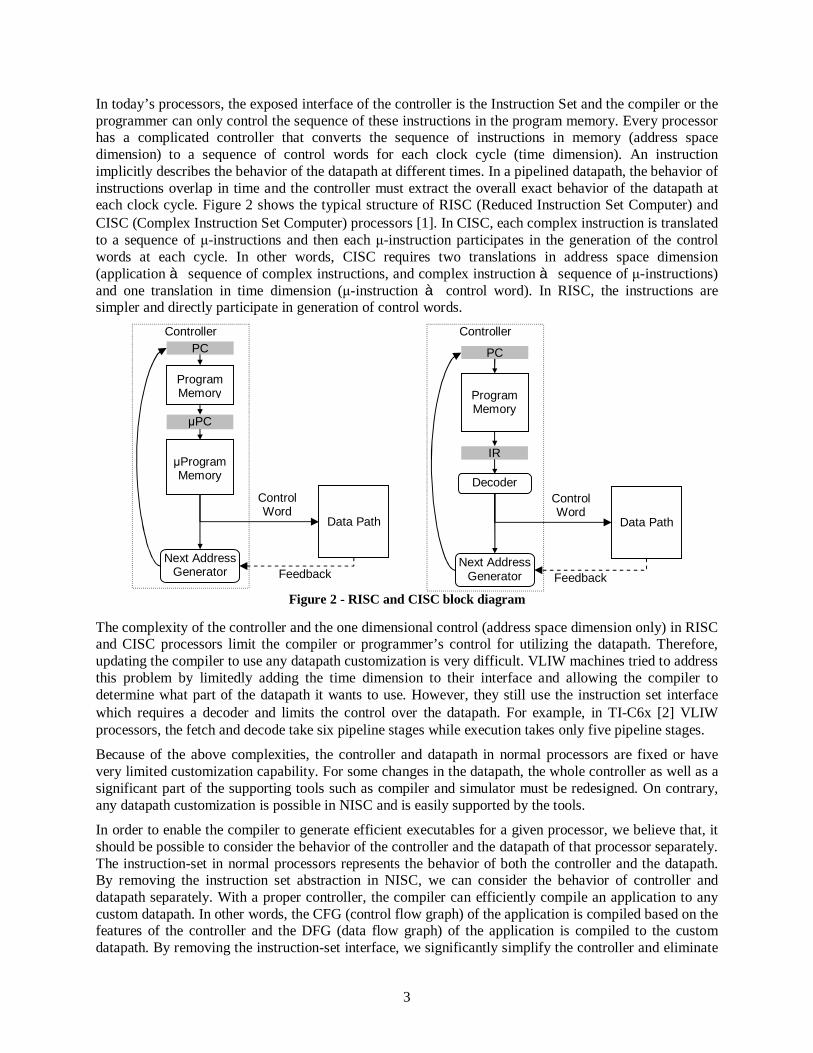
2 NISC’s View of the Processor In general a processor is a sequential hardware that can be viewed as a controller and a datapath as shown in Figure 1. In each step, the controller generates control bits for the datapath to perform a specific task and gets a feedback from datapath to determine the state of the circuit in the next step. To execute an application efficiently, we need to have an optimized datapath for the application and map (compile) the application on to the datapath by generating, customizing or configuring the controller. The utilization of the datapath depends on its controllability and the interface that the controller provides for this purpose.
Figure 1 - General sequential hardware
Controller Data Path
Feedback
Control Word
3
In today’s processors, the exposed interface of the controller is the Instruction Set and the compiler or the programmer can only control the sequence of these instructions in the program memory. Every processor has a complicated controller that converts the sequence of instructions in memory (address space dimension) to a sequence of control words for each clock cycle (time dimension). An instruction implicitly describes the behavior of the datapath at different times. In a pipelined datapath, the behavior of instructions overlap in time and the controller must extract the overall exact behavior of the datapath at each clock cycle. Figure 2 shows the typical structure of RISC (Reduced Instruction Set Computer) and CISC (Complex Instruction Set Computer) processors [1]. In CISC, each complex instruction is translated to a sequence of μ-instructions and then each μ-instruction participates in the generation of the control words at each cycle. In other words, CISC requires two translations in address space dimension (application à sequence of complex instructions, and complex instruction à sequence of μ-instructions) and one translation in time dimension (μ-instruction à control word). In RISC, the instructions are simpler and directly participate in generation of control words.
Figure 2 - RISC and CISC block diagram
The complexity of the controller and the one dimensional control (address space dimension only) in RISC and CISC processors limit the compiler or programmer’s control for utilizing the datapath. Therefore, updating the compiler to use any datapath customization is very difficult. VLIW machines tried to address this problem by limitedly adding the time dimension to their interface and allowing the compiler to determine what part of the datapath it wants to use. However, they still use the instruction set interface which requires a decoder and limits the control over the datapath. For example, in TI-C6x [2] VLIW processors, the fetch and decode take six pipeline stages while execution takes only five pipeline stages.
Because of the above complexities, the controller and datapath in normal processors are fixed or have very limited customization capability. For some changes in the datapath, the whole controller as well as a significant part of the supporting tools such as compiler and simulator must be redesigned. On contrary, any datapath customization is possible in NISC and is easily supported by the tools.
In order to enable the compiler to generate efficient executables for a given processor, we believe that, it should be possible to consider the behavior of the controller and the datapath of that processor separately. The instruction-set in normal processors represents the behavior of both the controller and the datapath. By removing the instruction set abstraction in NISC, we can consider the behavior of controller and datapath separately. With a proper controller, the compiler can efficiently compile an application to any custom datapath. In other words, the CFG (control flow graph) of the application is compiled based on the features of the controller and the DFG (data flow graph) of the application is compiled to the custom datapath. By removing the instruction-set interface, we significantly simplify the controller and eliminate
Controller
Data Path
Feedback
Control Word
Program Memory
PC
μPC
μProgram Memory
Next Address Generator
Controller
Data Path
Feedback
Control Word
Program Memory
PC
IR
Decoder
Next Address Generator
4
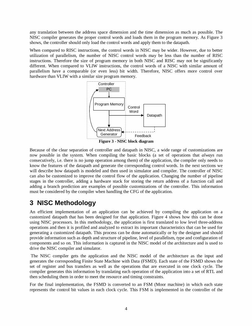
any translation between the address space dimension and the time dimension as much as possible. The NISC compiler generates the proper control words and loads them in the program memory. As Figure 3 shows, the controller should only load the control words and apply them to the datapath.
When compared to RISC instructions, the control words in NISC may be wider. However, due to better utilization of parallelism, the number of NISC control words may be less than the number of RISC instructions. Therefore the size of program memory in both NISC and RISC may not be significantly different. When compared to VLIW instructions, the control words of a NISC with similar amount of parallelism have a comparable (or even less) bit width. Therefore, NISC offers more control over hardware than VLIW with a similar size program memory.
Figure 3 - NISC block diagram
Because of the clear separation of controller and datapath in NISC, a wide range of customizations are now possible in the system. When compiling the basic blocks (a set of operations that always run consecutively, i.e. there is no jump operation among them) of the application, the compiler only needs to know the features of the datapath and generate the corresponding control words. In the next sections we will describe how datapath is modeled and then used in simulator and compiler. The controller of NISC can also be customized to improve the control flow of the application. Changing the number of pipeline stages in the controller, adding a hardware stack for storing the return address of a function call and adding a branch prediction are examples of possible customizations of the controller. This information must be considered by the compiler when handling the CFG of the application.
3 NISC Methodology An efficient implementation of an application can be achieved by compiling the application on a customized datapath that has been designed for that application. Figure 4 shows how this can be done using NISC processors. In this methodology, the application is first translated to low level three-address operations and then it is profiled and analyzed to extract its important characteristics that can be used for generating a customized datapath. This process can be done automatically or by the designer and should provide information such as depth and structure of pipeline, level of parallelism, type and configuration of components and so on. This information is captured in the NISC model of the architecture and is used to drive the NISC compiler and simulator.
The NISC compiler gets the application and the NISC model of the architecture as the input and generates the corresponding Finite State Machine with Data (FSMD). Each state of the FSMD shows the set of register and bus transfers as well as the operations that are executed in one clock cycle. The compiler generates this information by translating each operation of the application into a set of RTL and then scheduling them in order to meet the resource and timing constraints.
For the final implementation, the FSMD is converted to an FSM (Moor machine) in which each state represents the control bit values in each clock cycle. This FSM is implemented in the controller of the
Controller
Datapath
Feedback
Control Word
Program Memory
PC
Next Address Generator

5
NISC processor. Depending on the size and complexity of the FSM and the design constraints, such as area and timing, the controller can be implemented in two possible ways:
• For simple FSMs, the controller can be synthesized using the standard cell libraries. A commercial synthesis tool, such as Design Compiler, can do the synthesis from the description of the FSM.
• For more complex FSMs, the controller can be implemented using a memory and a program counter (PC). The control words are stored in the memory and selected by PC.
The FSMD is also used to generate a cycle-accurate simulation model of the architecture. The simulator gets the sequence of the control words and simulates them on the model of the target NISC processor. Since NISC does not have any instruction-set, there will be no functional simulator in the traditional sense of it. The functionality of the application is validated by compiling and running the application itself or the equivalent 3-address operations. The cycle-accurate simulator can be used for both validating the correctness of the timing and functionality of the compiler’s output; and providing performance metrics such as speed and energy consumption for the Model Generator. The performance results of the simulator can be analyzed to fine tune the structure of the customized NISC processor.
Figure 4 shows the overall NISC methodology. The NISC processor model plays the key role in this methodology. Its structure determines the flexibility of the analyzer or designer for suggesting more optimized processors. It also affects the quality and complexity of the simulator and compiler.
FSMD
3 address code
NISC CompilerNISC Architecture
C-Compiler
Application
Architecture Generator
RTL Generator
Synthesizable RTL
Cycle-Accurate Simulator
Commercial Synthesis Tool
CW Generator
Control Words
(a) Model Generator
(d) Synthesizer
(b) Compiler
(c) Simulator
Figure 4 - NISC methodology
6
4 NISC Processor Model The NISC processor model is used mainly for three purposes:
3. Translating application operations to register transfers by the compiler and generating the corresponding FSMD.
4. Constructing the control words from the set of register transfers.
5. Decoding the control words back to their corresponding register transfers by simulator.
Our NISC model includes three category of information: the clock frequency, model of controller, and model of datapath. The model of controller captures the functionality of “Next Address Generator” unit, number of pipeline stages in the controller and the branch delay or the branch prediction strategy. This model is used during compilation and translation of the CFG of the input application. The model of datapath captures the flow and timing of possible data transfers in the processor as well as the mapping between the control bits of the units and their functionality. The model of datapath is in fact a netlist of the components describing their connectivity. The model of components captures information such as timing between the ports of component, and the functionality of the component. Details of model of datapath are described in Section 4.1.
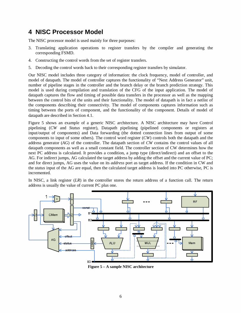
Figure 5 shows an example of a generic NISC architecture. A NISC architecture may have Control pipelining (CW and Status register), Datapath pipelining (pipelined components or registers at input/output of components) and Data forwarding (the dotted connection lines from output of some components to input of some others). The control word register (CW) controls both the datapath and the address generator (AG) of the controller. The datapath section of CW contains the control values of all datapath components as well as a small constant field. The controller section of CW determines how the next PC address is calculated. It provides a condition, a jump type (direct/indirect) and an offset to the AG. For indirect jumps, AG calculated the target address by adding the offset and the current value of PC; and for direct jumps, AG uses the value on its address port as target address. If the condition in CW and the status input of the AG are equal, then the calculated target address is loaded into PC otherwise, PC is incremented.
In NISC, a link register (LR) in the controller stores the return address of a function call. The return address is usually the value of current PC plus one.
Figure 5 – A sample NISC architecture
7
In addition to standard components, the datapath can have pipelined and multi-cycle components. For example in Figure 5, ALU, MUL and Mem are single-cycle, pipelined and multi-cycle components, respectively.
There is no limitation on the connections of components in the datapath. If the input of a component comes from multiple sources, a Bus or a Multiplexer is used to select the actual input. The buses are explicitly modeled and we assume one control bit per each writer to the bus. The multiplexers are implicit and we assume log2
n control bits for n writers.
In this section, we first describe the model of datapath and then review the modeling and support of multi-cycle components as well as pipelined datapaths.
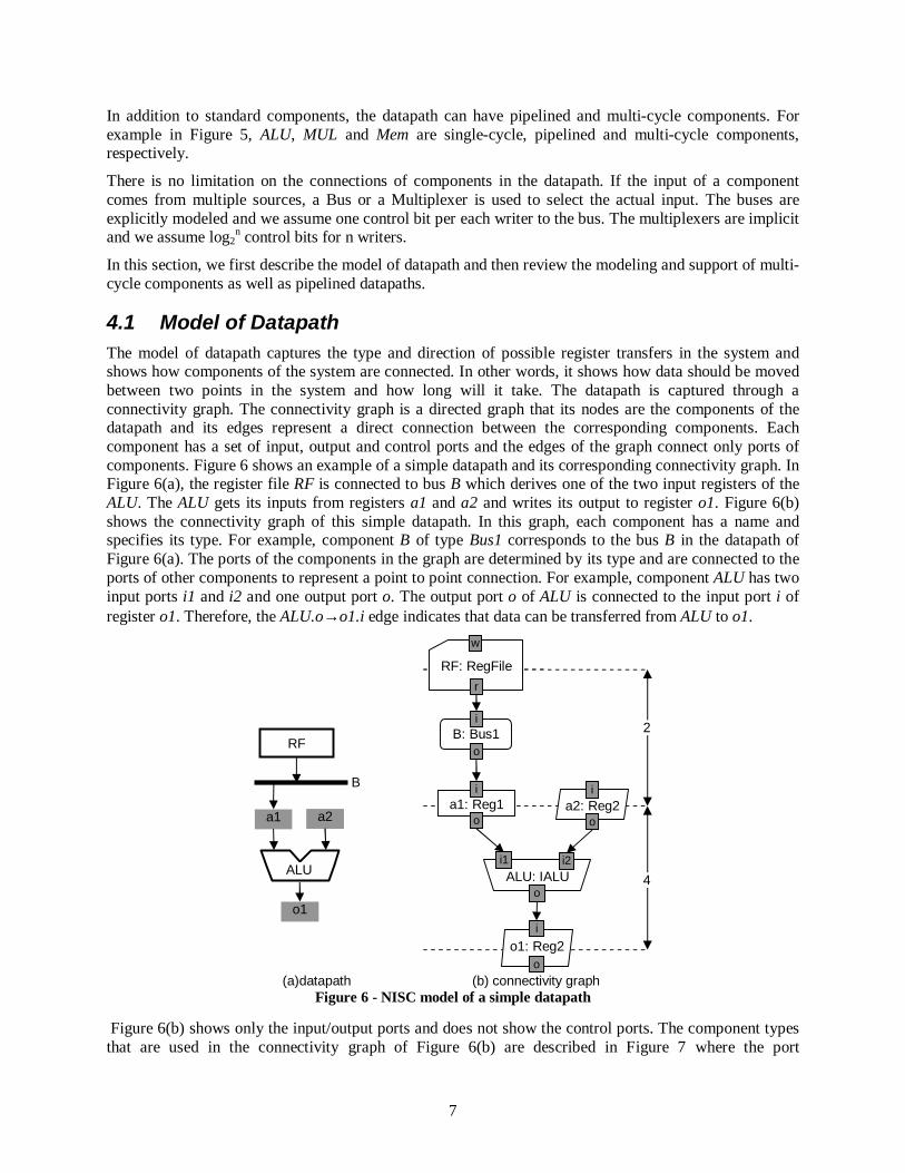
4.1 Model of Datapath The model of datapath captures the type and direction of possible register transfers in the system and shows how components of the system are connected. In other words, it shows how data should be moved between two points in the system and how long will it take. The datapath is captured through a connectivity graph. The connectivity graph is a directed graph that its nodes are the components of the datapath and its edges represent a direct connection between the corresponding components. Each component has a set of input, output and control ports and the edges of the graph connect only ports of components. Figure 6 shows an example of a simple datapath and its corresponding connectivity graph. In Figure 6(a), the register file RF is connected to bus B which derives one of the two input registers of the ALU. The ALU gets its inputs from registers a1 and a2 and writes its output to register o1. Figure 6(b) shows the connectivity graph of this simple datapath. In this graph, each component has a name and specifies its type. For example, component B of type Bus1 corresponds to the bus B in the datapath of Figure 6(a). The ports of the components in the graph are determined by its type and are connected to the ports of other components to represent a point to point connection. For example, component ALU has two input ports i1 and i2 and one output port o. The output port o of ALU is connected to the input port i of register o1. Therefore, the ALU.o→o1.i edge indicates that data can be transferred from ALU to o1.
(a)datapath (b) connectivity graph
Figure 6 - NISC model of a simple datapath
Figure 6(b) shows only the input/output ports and does not show the control ports. The component types that are used in the connectivity graph of Figure 6(b) are described in Figure 7 where the port
ALU: IALU i1 i2
o 4
2
a1: Reg1 o
i a2: Reg2
i
o
B: Bus1 o
i
o1: Reg2 i
o
RF: RegFile
r
w
RF
B
a1 a2
ALU
o1
8
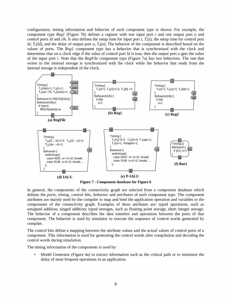
configuration, timing information and behavior of each component type is shown. For example, the component type Reg1 (Figure 7b) defines a register with one input port i and one output port o and control ports ld and clk. It also defines the setup time for input port i, Ts(i), the setup time for control port ld, Ts(ld), and the delay of output port o, Td(o). The behavior of the component is described based on the values of ports. The Reg1 component type has a behavior that is synchronized with the clock and determines that on a clock edge if the value of control port ld is true, then the output port o gets the value of the input port i. Note that the RegFile component type (Figure 7a) has two behaviors. The one that writes to the internal storage is synchronized with the clock while the behavior that reads from the internal storage is independent of the clock.
Figure 7 - Component database for Figure 6
In general, the components of the connectivity graph are selected from a component database which defines the ports, timing, control bits, behavior and attributes of each component type. The component attributes are mainly used by the compiler to map and bind the application operation and variables to the components of the connectivity graph. Examples of these attributes are: typed operations, such as unsigned addition, singed addition; typed storages, such as floating point storage, short integer storage. The behavior of a component describes the data transfers and operations between the ports of that component. The behavior is used by simulator to execute the sequence of control words generated by compiler.
The control bits define a mapping between the attribute values and the actual values of control ports of a component. This information is used for generating the control words after compilation and decoding the control words during simulation.
The timing information of the components is used by:
• Model Generator (Figure 4a) to extract information such as the critical path or to minimize the delay of most frequent operations in an application.
(d) IALU
Timing:{ Tpp(i1→o)=1.5; Tpp(i2→o)=1; Tpp(op→o)=1;
} Behavior:{ switch(op){ case ADD: o= i1+i2; break; case SUB: o=i1-i2; break;…
}; }
i1 i2
o
op
(a) RegFile
Timing:{ Ts(rIdx)=1; Td(r)=1; Ts(w)=.75; Ts(wIdx)=1;
} Behavior:{r=REGS[rIdx];} Behavior(clk):{ If (wen) REGS[wIdx]=w; }
w
r
rIdx
wIdx wen clk
(f) Bus1
Timing:{} Behavior:{ if (b1) o=i; }
o
i
b1
(b) Reg1
Timing:{ Ts(i)=1; Td(o)=1.5; Ts(ld) =1;
} Behavior(clk):{
if (ld) o=i;
} o
i
ld
clk
(c) Reg2
Timing:{ Ts(i)=1; Td(o)=1; Ts(ld)=1;
} Behavior(clk):{
if (ld) o=i;
} o
i
ld clk
(e) P-IALU
Timing:{ Ts(i1)=0.5; Ts(i2)=0; Ts(op)=1;
Td(o)=1; #stages=1; } Behavior:{ switch(op){ case ADD: o= i1+i2; break; case SUB: o=i1-i2; break;…
}; }
i1 i2
o
op

9
• Compiler (Figure 4b) to determine the number of required clock cycles for each register transfer or operation.
• Simulator (Figure 4c) to validate the timings and evaluate the performance.
The timing information of all components (both storage and functional units) is represented in four different forms:
• Setup time Ts(x) for input or control ports. It shows the amount of time that the data must be available on ports x before the clock edge.
• Output Delay Td(x) for output ports. It shows the amount of time after the clock edge that it takes for the value to appear on output port x.
• Port-to-Port Delay Tpp(x→y) from input or control ports to output ports. It shows the amount of time that it takes for the effect of the value of input or control port x to appear on the output port y.
• Sequence relation or time difference Tdif(x<y) between any two ports. It shows the amount of time that an event on y should or will happen after an event on x. Note that all other timing forms can be represented with Tdif. For example, Ts(x) = Tdif(x<clk) and Td(x)=Tdif(clk<x). However, the other forms carry more semantic information that can be used by the tools.
The structure of ports (and hence the interpretation of timing information) for each component depend on its type. We define seven types of components as follows:
1. Register is a single-storage clocked component that has at least one input port and one output port. Figure 7b shows an example register component type.
2. Register File is a multi-storage clocked component. For each write or read port, there is at least one address control port whose value determines which internal storage element is read by the corresponding output port or is written by the corresponding input port. Usually, for each input port a single bit control port enables the write. Writes are always synchronized with the clock, i.e. the address and input port value are used to update the internal storage only at the edge clock. Therefore, for input ports and their corresponding address control ports a setup time, Ts, must be defined. The reads from register file are independent of the clock and any time the value of an output address changes, the value of the corresponding internal storage appears on the output port. Therefore, for an output port r and its corresponding control port rIidx, Tpp(rIidx→r) must be defined. Other control ports may be used for enabling/disabling the reads or writes. Usually, the read/write addresses of a register file are directly controlled by CW. Figure 7a shows an example register file component type.
3. Bus is component that has multiple input and control ports but one output port. It does not have any internal storage and therefore is not clocked. Figure 7f shows an example bus component type.
4. Memory is also a multi-storage component similar to Register File. However, it usually works as combinational logic (clock independent) and may use only one address control port to determine the internal storage to be used for read or write. Typically, a chip-enable control signal enables/disables the memory and a read-write control signal determines the behavior of the memory. The timing protocol of memory can be captures through several Tpp and Tdif timings. Usually, the load/store address of a memory comes from datapath.
5. Computational Unit is a combinational unit that performs an operation on the input data and produces an output. It may have control signals for determining the type of its operation. Figure 7d shows an example computational unit component type.
10
6. Pipelined Computational Unit is similar to the Computational Unit but has a specific number of internal pipeline stages. Therefore, instead of having port-to-port delays, a setup time is defined for the input and control ports relative to the first internal pipeline stage and an output delay is defined for the output ports relative to the last internal pipeline stage. The number of internal pipeline stages of such components must also be captured by the model. Figure 7e shows an example pipelined computational unit component type.
7. Compound component is an abstraction of a connectivity graph that can be used as a component in another connectivity graph. By using this component, the model can support hierarchical designs. The ports, timing and behavior of this component are defined by its corresponding connectivity graph. Before any processing in the tools, these components may be expanded and the connectivity graph if flattened.
To enable further customization of the datapath towards the characteristics of the application, the NISC datapath model supports multi-cycle component and pipelined controller/datapath to provide faster and better performance. Pipelining not only improves the resource utilization but also can help reducing the clock period. By supporting multi-cycle component, the clock period is no longer limited by the critical path. In the next sections, we describe how these features are captures and review their possible effects on the simulator and compiler.
4.2 Multi-cycle and pipelined component support A multi-cycle component takes more than one clock cycle to generate its output. This means the clock frequency is not necessarily bounded by the critical path. In the NISC processor model, whenever the clock period is less than the delay of component, that component should be treated as multi-cycle. Therefore, no special representation is needed for such components in the model of datapath. Whenever a register transfer involves a multi-cycle component, the NISC compiler must expand the corresponding control bits over multiple cycles during the generation of control words. In this way, the control words guarantee the correct execution and therefore the simulator does not need to handle multi-cycle components different than the normal ones.
To understand this concept better, consider the following example based on datapath of Figure 6. Assume the operation x=y+z is translated to o1=ALU(+, a1, a2) register transfer which takes four units according to the connectivity graph of Figure 6 and component database information of Figure 7. If the clock period is at least 4 units, then the whole operation can be done in one cycle and the control word would be: clock n: o.load = 1; ALU.op = +;
Now assume that the clock period is only two units. For a correct execution, the control signals of the ALU must remain unchanged during two consecutive cycles and the result must be loaded in the output register at the end of the second cycle. Therefore the control word would be: clock n: ALU.op = +; clock n+1: o1.load = 1; ALU.op = +;
A multi-cycle component can be pipelined. This means that the control and input values need to remain stable only during one (first) cycle but the output will be generated after multiple cycles. A pipelined component has internal registers that carry the intermediate data and control values. Assume that the ALU component of Figure 6 is one stage pipelined and Ts(i1)=0.5, Ts(i2)=0, Td(o)=1 (Figure 7e). For the above example, the control signals of ALU that select addition operation are only needed in the first cycle of execution. The actual control bits of the rest of pipeline stages of the component are generated internally. Therefore, with a clock period of two units, the control word would be: clock n: ALU.op = +; clock n+1: o.load = 1;
11
All of these cases can be simply detected by comparing the clock period with the timing information of components models of datapath.
4.3 Pipelined datapath Pipelining is a powerful parallelizing feature that inevitably appears in any modern processor. The pipeline in a NISC processor is divided into two consecutive parts: controller pipeline and datapath pipeline. The controller pipeline generates the control words or fetches them from the memory. This part of the pipeline is very simple and almost identical in all NISC processors. The second part of the processor pipeline is the datapath pipeline. The flow of data in the datapath pipeline is solely controlled by the control word. In connectivity graph of the datapath, the stages of the pipeline are represented by registers and pipelined computational units. Since the control words describe the complete behavior of the datapath pipeline, the simulator can easily handle any complex pipeline structure by simply applying the control bits to the components and simulating individual component behaviors. However, the compiler must generate the exact and detailed behavior of the pipeline and therefore, the complexity and structure of the pipeline have a direct effect on the complexity of the algorithms used in the compiler. In Section 6, we briefly describe what the compiler needs to do to handle the pipeline.
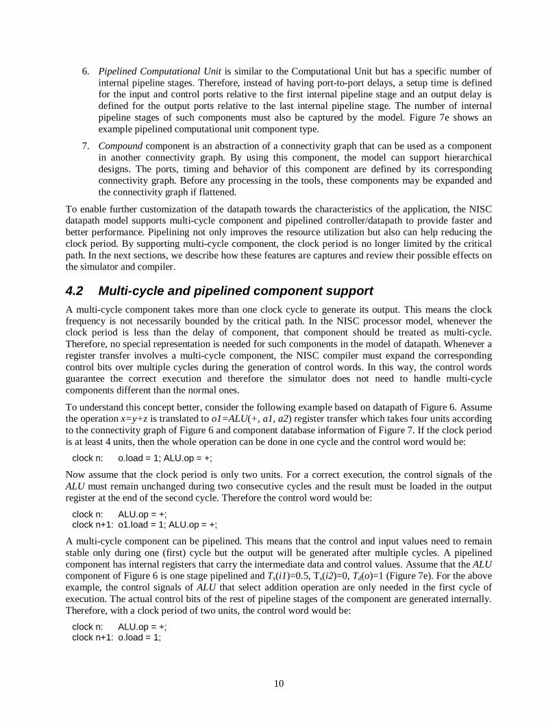
5 Simulation The simulator is used for both validating the output of the compiler and evaluating the performance of the NISC processor. The output of the compiler has both timing and functionality information that must be validated. Validating the timing of register transfers can be statically done using the connectivity graph and comparing its information against the value of control bits in the control words. Therefore, the simulator needs only to validate the functionality of the output of the compiler. On the other hand, since each control word represents the behavior of the processor in one clock cycle, the number of executed control words is equal to the number of clock cycles that the execution takes. In this way, a functional simulation of the control words also represents the performance of the processor.
Considering the general structure of a NISC processor shown in Figure 3, the main loop of the simulator is very simple and straight forward. Figure 8 shows the pseudo code of the simulation main loop. In each cycle of simulation, first the control word corresponding to current PC is read from memory; and then, the datapath pipeline is executed using the contents of the current control word. At the end of each cycle, the next value of PC is calculated using the content of control word and the feedback from datapath. The feedback from datapath typically includes the value of status bits and a possible target address for indirect jumps. The control word indicates whether the PC must be incremented or updated with the target address.
ControlWord cw = 0; while (not end of program) { cw = Mem[PC]; execute ( cw ); PC = calculate next PC from cw and datapath feedback; }
Figure 8 - Pseudo code of the simulation main loop
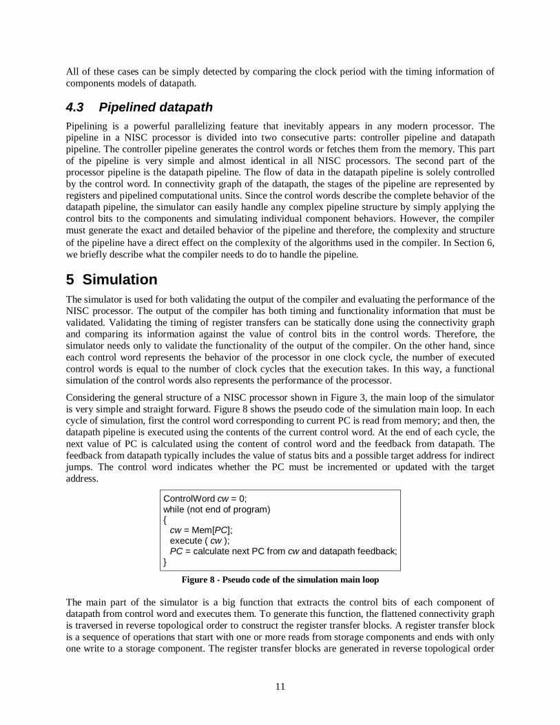
The main part of the simulator is a big function that extracts the control bits of each component of datapath from control word and executes them. To generate this function, the flattened connectivity graph is traversed in reverse topological order to construct the register transfer blocks. A register transfer block is a sequence of operations that start with one or more reads from storage components and ends with only one write to a storage component. The register transfer blocks are generated in reverse topological order
12
to ensure all storages are read before they are written. Figure 9 shows the simulation main function of the datapath of Figure 6. In this pseudo code, the control word cw contains all of the control bits of the components of the datapath. For example, a1 in Figure 6 is a Reg1 component type (Figure 7b) and therefore has an ld control bit that is connected to cw.a1.ld. During the traversal of the connectivity graph, the behavior of each component is copied from its corresponding component type to the body of execute function. In the second register transfer block of Figure 9, lines 15, 17, 19 are the behaviors of the RegFile, Bus1 and Reg1 from Figure 7a, Figure 7f and Figure 7b, respectively. Also, for every edge in the connectivity graph, an assignment is generated in the simulation function. For example, in the second register transfer block of Figure 9, lines 16 and 18 represent the RF.r→B.i and B.o→a1.i edges of the connectivity graph of Figure 6(b) respectively.
01 02 03 04 05 06 07 08 09 10 11 12 13 14 15 16 17 18 19 20 21 22 23 24 25
void execute(ControlWord cw) {
//Register transfer Block 1 ALU.i2 = a2.o; ALU.i1 = a1.o; switch (cw.ALU.op) { case Add: ALU.o = ALU.i1 + ALU.i2; break; case Sub: ALU.o = ALU.i1 - ALU.i2; break; //… } o1.i = ALU.o;
if (cw.o1.ld) o1.o = o1.i; // Register transfer Block 2 RF.r = RF.regs[cw.RF.idx]; B.i = RF.r; if (cw.B.b1) B.o = B.i; a1.i = B.o; if (cw.a1.ld) a1.o = a1.i; // Register transfer Block 3 //other part of the datapath that writes into a2 a1.i = … if (cw.a2.ld) a2.o = a1.i; }
Figure 9 - Main simulation function for datapath of Figure 6
The generated code for the execute function in the simulator is compiled and optimized by a conventional C or C++ compiler. During this optimization, each register transfer block is reduced to manipulation of register data only.
6 Compilation To execute an application on a given datapath, the compiler must translate each operations of the application to sequences of register transfers by generating proper control words for each cycle. In this section we detail the NISC compiler internal phases and its place in the NISC methodology.
13
Scheduler
FSMD
3 address code
Register Binding
CDFG Constructor
CDFGOrder of basic
blocks in memorygenerated
automatically or manually
Target Architecture
pre-binder
C-Compiler
C Application
Compiler
CW Generator
Control Words
Architecture Preprocessor
Figure 10- NISC compiler flow Figure 4b
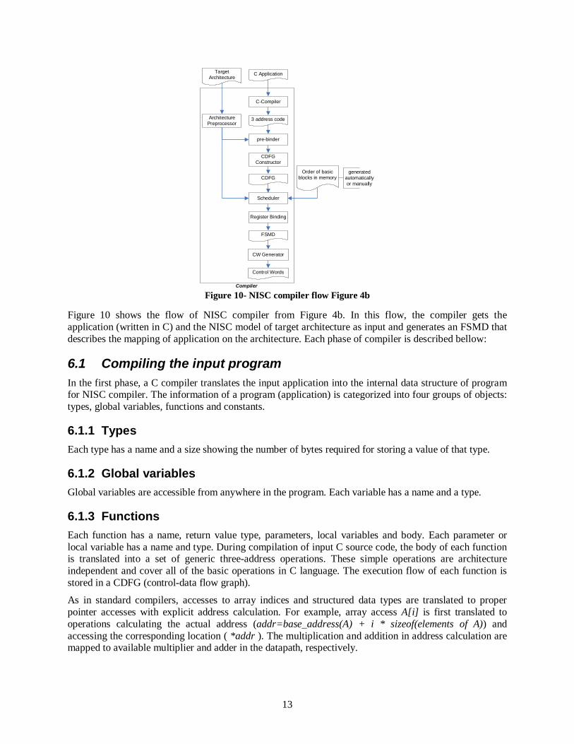
Figure 10 shows the flow of NISC compiler from Figure 4b. In this flow, the compiler gets the application (written in C) and the NISC model of target architecture as input and generates an FSMD that describes the mapping of application on the architecture. Each phase of compiler is described bellow:
6.1 Compiling the input program In the first phase, a C compiler translates the input application into the internal data structure of program for NISC compiler. The information of a program (application) is categorized into four groups of objects: types, global variables, functions and constants.
6.1.1 Types Each type has a name and a size showing the number of bytes required for storing a value of that type.
6.1.2 Global variables Global variables are accessible from anywhere in the program. Each variable has a name and a type.
6.1.3 Functions Each function has a name, return value type, parameters, local variables and body. Each parameter or local variable has a name and type. During compilation of input C source code, the body of each function is translated into a set of generic three-address operations. These simple operations are architecture independent and cover all of the basic operations in C language. The execution flow of each function is stored in a CDFG (control-data flow graph).
As in standard compilers, accesses to array indices and structured data types are translated to proper pointer accesses with explicit address calculation. For example, array access A[i] is first translated to operations calculating the actual address (addr=base_address(A) + i * sizeof(elements of A)) and accessing the corresponding location ( *addr ). The multiplication and addition in address calculation are mapped to available multiplier and adder in the datapath, respectively.

14
6.1.4 Constants Similar to global variables, all constants of the program are stored separately. Each constant has a value and a type and is treated as a read-only variable.
6.2 Architecture preprocessor Before the NISC model of architecture can be used by the compiler, its information must be processed to extract the compiler related information such as different pipeline paths; structure of controller pipeline; and mapping of operations and functional units. The architecture preprocessor phase extracts the information and stores them in proper data structures.
6.3 Pre-binder The pre-binder gets the information of the target architecture and binds the variables of the program to proper storages. We define the following types of storage accesses depending on where the data value is stored:
1. Immediate: Data is stored directly in the control word and is usually used for small constant values.
2. RegisterDirect: Data is stored in a register.
3. RegisterIndex: Data is stored in a register file and accessed by a filed in the control word.
4. MemoryDirect: Data is stored in memory or scratch pad and addressed by a constant. The constant itself may use any addressing mode.
5. MemoryIndex: data stored in memory or scratch pad and addressed by a constant and a register (base). The constant itself may use any addressing mode. The register is an individual register or one in a register file.
By default, the pre-binder uses the following storage binding for different types of variables:
1. Global variables are accessed with MemoryDirect if no data segment register is defined. Otherwise, MemoryIndex access mode is used for binding global variables.
2. Return value of functions are accessed with RegisterDircet, RegisterIndex, MemoryDirect or MemoryIndex. The actual access mode is specified in the architecture model.
3. Function parameters are accessed with MemoryIndex (stack based) mode.
4. Local variables are accessed with RegisterIndex mode if their address is never used. Otherwise, they are bound using MemoryIndex (stack based) mode.
5. Constants can be bound in any of the following ways:
• Immediate mode can be used to store the constants in the control word. This option is the fastest but requires longer CW. Usually, the Immediate access mode is only used for small constants values, e.g. less than 8 bits.
• RegisterDirect or RegisterIndex mode can be used to store the constant in a register or register file. This option is relatively fast and results in smaller CW size, but requires more storage elements.
• MemoryDirect mode can be used for storing constants in a memory. This option is slow but is good for storing very large constant values.
6. Temporary values in function bodies are not bounded in pre-binding phase.
15
In the pre-binding phase, only unbounded variables are bounded. Therefore, the user can also manually bind any variable (including temporaries) and such bindings will not be modified by the pre-binder or in the register binding phase.
To avoid the complications of pointer analysis, any load/store operation uses the main memory by default but user can manually set their corresponding storage. This storage must eventually match storage of the variable that is being loaded/stored.
Unless all variables in a program are manually bounded, the automatic binding algorithm requires the target architecture to provide: a stack pointer register for function calls; a fixed point and a floating point register file as the default storage of unbounded fixed point and floating point variables, respectively.
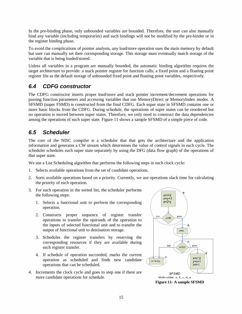
6.4 CDFG constructor The CDFG constructor inserts proper load/store and stack pointer increment/decrement operations for passing function parameters and accessing variables that use MemoryDirect or MemoryIndex modes. A SFSMD (super FSMD) is constructed from the final CDFG. Each super state in SFSMD contains one or more basic blocks from the CDFG. During schedule, the operations of super states can be reordered but no operation is moved between super states. Therefore, we only need to construct the data dependencies among the operations of each super state. Figure 11 shows a sample SFSMD of a simple piece of code.
6.5 Scheduler The core of the NISC compiler is a scheduler that that gets the architecture and the application information and generates a CW stream which determines the value of control signals in each cycle. The scheduler schedules each super state separately by using the DFG (data flow graph) of the operations of that super state.
We use a List Scheduling algorithm that performs the following steps in each clock cycle:
1. Selects available operations from the set of candidate operations.
2. Sorts available operations based on a priority. Currently, we use operations slack time for calculating the priority of each operation.
3. For each operation in the sorted list, the scheduler performs the following steps:
1. Selects a functional unit to perform the corresponding operation.
2. Constructs proper sequence of register transfer operations to transfer the operands of the operation to the inputs of selected functional unit and to transfer the output of functional unit to destination storage.
3. Schedules the register transfers by reserving the corresponding resources if they are available during each register transfer.
4. If schedule of operation succeeded, marks the current operation as scheduled and finds new candidate operations that can be scheduled.
4. Increments the clock cycle and goes to step one if there are more candidate operations for schedule.
Figure 11- A sample SFSMD
16
In addition to the delay of the operations of a program, the compiler also needs to know the delay of changing the current state. If the target architecture does not have any controller pipeline, then any state change always takes one cycle. However, in presence of controller pipelining, a state change may take one or more than one cycle depending on the pipeline length of controller. The programs that are run on such architectures are usually more complex and therefore, the pipelined controller is usually implemented by a memory. In a memory based implementation of the controller, the control words are stored in a memory; the states are mapped to memory addresses; and the current state is represented with a program counter (PC) register. For every state change, if the current state and next state are stored in two consecutive memory addresses, PC is incremented; otherwise the address of next state is loaded into PC. While incrementing the PC takes one cycle, loading a new address into PC will take more than one cycle when the controller is pipelined. Therefore, in order to extract the timing of a state change we need to know the order of states in memory. This information is extracted from the order of basic blocks in the memory, shown in Figure 10. In NISC compiler tool flow, this order is given as an input or generated automatically and is preserved in the output to maintain the correctness of the schedule. Figure 11 shows an example SFSMD in which the circles represent super states containing one or more basic blocks of the CDFG. Each super state is eventually converted to a serial sequence of states each representing one clock cycle. Therefore, the cost of changing states can be extracted from the super states as well. Because of the given order of super states in Figure 11, changing state from a to e, c to e or d to c require generating new address (rather than incrementing PC). A pipelined controller will need multiple states for such transitions.
6.6 Register binder After assigning operations to control steps by scheduler, the Register Binding phase, binds the temporary values of the basic blocks that were not bound in pre-binding. This is similar to a typical register allocation phase in a traditional compiler.
7 Experiments We currently have implemented a proof-of-concept compiler that gets the model of a NISC architecture and compiles a given program on that architecture by generating the proper control words. To evaluate the functionality and efficiency of the current NISC compiler, we compiled five programs on six NISC architectures as well as the MIPS 4K [3]. The programs were as follows:
• Ones Counter: a simple ones counter that counts the number of ones in a 32 bit integer.
• Bdist2: the bdist2 function in the MPEG2 encoder [4] that calculates the absolute distance error between a 16×h block and a bidirectional prediction.
• DCT: the Discrete Cosine Transform algorithm.
• FFT: Fast Fourier Transform algorithem.
• Sort: the bubble sort algorithm.
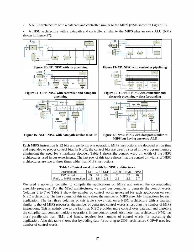
We used the six following NISC architectures:
• A NISC architecture without any pipelining (NP shown in Figure 12).
• A NISC architecture with only controller pipelining (CP shown in Figure 13).
• A NISC architecture with both controller and datapath pipelining (CDP shown in Figure 14).
• A NISC architecture with controller and datapath pipelining as well as data forwarding (CDP+F shown in Figure 15).
17
• A NISC architecture with a datapath and controller similar to the MIPS (NM1 shown in Figure 16).
• A NISC architecture with a datapath and controller similar to the MIPS plus an extra ALU (NM2 shown in Figure 17).
PC
CW
+
LR
constRF
ALU Mem
address
status
CMem
PC
AG
CW
offset
+1 LR
MUL
B1
B3
B2
Figure 12- NP: NISC with no pipelining Figure 13- CP: NISC with controller pipelining RF
ALU Mem
CMem
PC
AG
CW
offset
+1 LR
MUL
const
statusstatus
R1 R4R2 R5 R7 R8
R9R6R3
address
B3
B1
B2
RF
ALU Mem
CMem
PC
AG
CW
offset
+1 LR
MUL
const
status
status R1 R4R2 R5 R7 R8
R9R6R3
address
B3
B1
B2
B4B5B6
Figure 14- CDP: NISC with controller and datapath
pipelining Figure 15- CDP+F: NISC with controller and
datapath pipelining + data forwarding
CMem
PC
AG
CW
offset
+1 LR
const
status
address
ABDB
B4
B1
B2
B3
RF
ALUMUL
P
AR DR
Mem
SP xSP
CMem
PC
AG
CW
offset
+1 LR
const
status
address
ABDB
B1
B2
B3
RF
ALUMUL
P
A R DR
Mem
S P x SP
ALU2
B6
B5
B4
Figure 16- NM1: NISC with datapath similar to MIPS Figure 17- NM2: NISC with datapath similar to
MIPS but having one extra ALU
Each MIPS instruction is 32 bits and performs one operation. MIPS instructions are decoded at run time and expanded to proper control bits. In NISC, the control bits are directly stored in the program memory eliminating the need for a hardware decoder. Table 1 shows the control word bit width of the NISC architectures used in our experiments. The last row of this table shows that the control bit widths of NISC architectures are two to three times wider than MIPS instructions.
Table 1- Control word bit width for NISC architectures Architecture NP CP CDP CDP+F NM1 NM2 CW bit width 59 59 69 81 82 87
Ratio to MIPS instruction 1.8 1.8 2.2 2.5 2.6 2.7
We used a gcc-mips compiler to compile the applications on MIPS and extract the corresponding assembly programs. For the NISC architectures, we used our compiler to generate the control words. Columns 2 to 7 of Table 2 show the number of control words generated for each application on each NISC architecture. The last column of this table show the number of MIPS assembly instructions for each application. The last three columns of this table shows that, on a NISC architecture with a datapath similar to that of MIPS processor, the number of generated control words is less than the number of MIPS instructions. This is mainly due to the fact that NISC provides more control over datapath and therefore the compiler can compact multiple operations in one control word. Also note that, architecture NM2 has more parallelism than NM1 and hence, requires less number of control words for executing the application. Also this table shows that by adding data-forwarding to CDP, architecture CDP+F uses less number of control words.
18
Table 2- Number of control words in NISC architectures and instructions in MIPS NP CP CDP CDP+F NM1 NM2 MIPS
Ones Counter 6 8 11 11 8 8 12 Bdist2 71 74 82 66 65 55 73 DCT 24 27 35 33 27 26 37 FFT 219 219 216 164 160 131 210 Sort 23 28 43 38 29 28 31
Table 3 compares the size of program memory of NISC architectures with that of MIPS. The numbers in this table are calculated from the following equation:
Ratio NISC program memory size vs. MIPS= control word bit with × # of control words
32 × # of MIPS instructions
The last two columns of this table show that the program memories of NM1 and NM2 architectures are almost twice larger than that of MIPS. However, the difference decreases when there is more parallelism in the application and the datapath. For example, although NM2 has wider control words compared to NM1, the program memory of applications such as FFT that have parallelism is smaller than the corresponding program memory of NM1. Since in NISC, no-op operations must be explicitly stored in the program memory, the structure of datapath can also affect the program memory size. For example, although NM1 and NM2 require smaller program memory than CDP and CDP+F, while having wider control words.
Table 3- Ratio of NISC to MIPS program memory size NP CP CDP CDP+F NM1 NM2
Ones Counter 0.92 1.23 1.98 2.32 1.71 1.81 Bdist2 1.79 1.87 2.42 2.29 2.28 2.05 DCT 1.20 1.35 2.04 2.26 1.87 1.91 FFT 1.92 1.92 2.22 1.98 1.95 1.70 Sort 1.37 1.67 2.99 3.10 2.40 2.46
Table 4 shows the average operation per control word of each application on different NISC architectures. The second column of this table shows the number of operations in each application (including reads and writes). The rest of table show the number of operations divided by the corresponding number of control words (Table 2).
Table 4- Average operation per control word in NISC architectures. #operations NP CP CDP CDP+F NM1 NM2
Ones Counter 10 1.67 1.25 0.91 0.91 1.25 1.25 Bdist2 100 1.41 1.35 1.22 1.52 1.54 1.82 DCT 35 1.46 1.30 1.00 1.06 1.30 1.35 FFT 248 1.13 1.13 1.15 1.51 1.55 1.89 Sort 37 1.61 1.32 0.86 0.97 1.28 1.32
Table 5 shows the compilation time of each application on each NISC architecture. The compilation times shown in this table exclude the time needed for converting the C language to generic 3-address operations. We used a standard compiler for generating the 3-address code. Note that for more limited architectures, the compiler must spend more time to generate the control words. The current implementation of the compiler is not optimized for speed and the compilation times are presented to show that although the NISC compiler is more sophisticated than a traditional instruction-set based compiler, the speed of current compiler is in an acceptable range.
Table 5- Compilation times (in seconds) NP CP CDP CDP+F NM1 NM2
Ones Counter 0.1 0.1 0.1 0.1 0.1 0.1 Bdist2 2.4 2.4 2.0 0.8 1.5 0.5 DCT 0.3 0.2 0.2 0.2 0.2 0.1 FFT 157.2 149.6 116.3 8.7 7.1 4.3
19
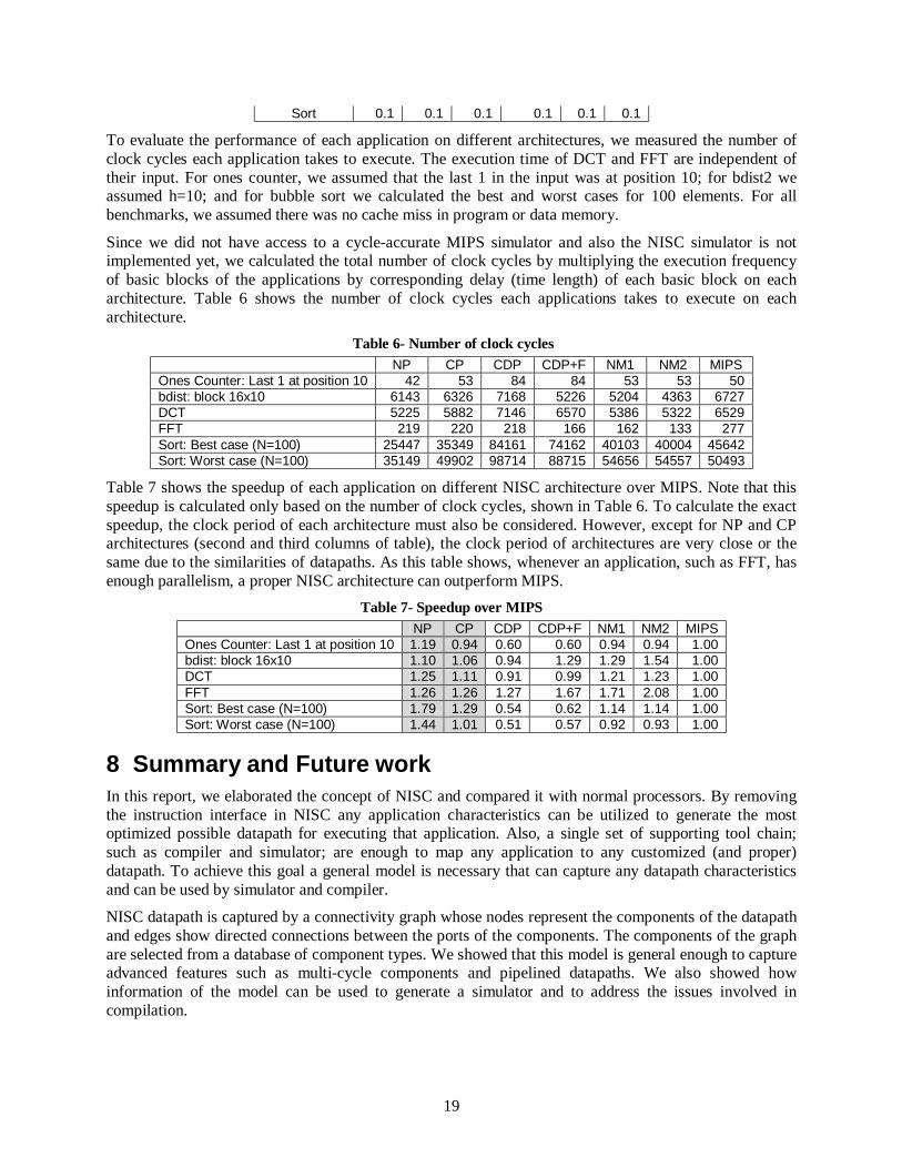
Sort 0.1 0.1 0.1 0.1 0.1 0.1
To evaluate the performance of each application on different architectures, we measured the number of clock cycles each application takes to execute. The execution time of DCT and FFT are independent of their input. For ones counter, we assumed that the last 1 in the input was at position 10; for bdist2 we assumed h=10; and for bubble sort we calculated the best and worst cases for 100 elements. For all benchmarks, we assumed there was no cache miss in program or data memory.
Since we did not have access to a cycle-accurate MIPS simulator and also the NISC simulator is not implemented yet, we calculated the total number of clock cycles by multiplying the execution frequency of basic blocks of the applications by corresponding delay (time length) of each basic block on each architecture. Table 6 shows the number of clock cycles each applications takes to execute on each architecture.
Table 6- Number of clock cycles NP CP CDP CDP+F NM1 NM2 MIPS
Ones Counter: Last 1 at position 10 42 53 84 84 53 53 50 bdist: block 16x10 6143 6326 7168 5226 5204 4363 6727 DCT 5225 5882 7146 6570 5386 5322 6529 FFT 219 220 218 166 162 133 277 Sort: Best case (N=100) 25447 35349 84161 74162 40103 40004 45642 Sort: Worst case (N=100) 35149 49902 98714 88715 54656 54557 50493
Table 7 shows the speedup of each application on different NISC architecture over MIPS. Note that this speedup is calculated only based on the number of clock cycles, shown in Table 6. To calculate the exact speedup, the clock period of each architecture must also be considered. However, except for NP and CP architectures (second and third columns of table), the clock period of architectures are very close or the same due to the similarities of datapaths. As this table shows, whenever an application, such as FFT, has enough parallelism, a proper NISC architecture can outperform MIPS.
Table 7- Speedup over MIPS NP CP CDP CDP+F NM1 NM2 MIPS
Ones Counter: Last 1 at position 10 1.19 0.94 0.60 0.60 0.94 0.94 1.00 bdist: block 16x10 1.10 1.06 0.94 1.29 1.29 1.54 1.00 DCT 1.25 1.11 0.91 0.99 1.21 1.23 1.00 FFT 1.26 1.26 1.27 1.67 1.71 2.08 1.00 Sort: Best case (N=100) 1.79 1.29 0.54 0.62 1.14 1.14 1.00 Sort: Worst case (N=100) 1.44 1.01 0.51 0.57 0.92 0.93 1.00
8 Summary and Future work In this report, we elaborated the concept of NISC and compared it with normal processors. By removing the instruction interface in NISC any application characteristics can be utilized to generate the most optimized possible datapath for executing that application. Also, a single set of supporting tool chain; such as compiler and simulator; are enough to map any application to any customized (and proper) datapath. To achieve this goal a general model is necessary that can capture any datapath characteristics and can be used by simulator and compiler.
NISC datapath is captured by a connectivity graph whose nodes represent the components of the datapath and edges show directed connections between the ports of the components. The components of the graph are selected from a database of component types. We showed that this model is general enough to capture advanced features such as multi-cycle components and pipelined datapaths. We also showed how information of the model can be used to generate a simulator and to address the issues involved in compilation.
20
The internal flow of current implementation of our NISC compiler was described here. We presented some preliminary experiments to show that the compiler can in fact get the architectural information from the NISC model rather than being fixed for a specific architecture. The results also showed that, on proper datapaths, the compiler can exploit the available parallelism of applications and generate codes that outperform that of a MIPS compiler. This is the first attempt for developing a NISC compiler. Clearly, there is a lot more improvements and compiler optimizations that can be added to the current implementation to make the NISC compiler even better than its current state.
Our future work focuses on adding more parallelizing optimizations to the compiler. To complete the NISC methodology (Figure 4); an architecture generator, a simulator and a synthesizer must also be implemented in future. These tools are beyond the scope of current project but are eventually necessary for exploiting the full range of benefits that NISC offers. The research on simulator and compiler will also help us verify the information and structure of the model and improve it, if necessary.
9 References [1] D. Gajski, "NISC: The Ultimate Reconfigurable Component," CECS Technical Report 03-28, October
1, 2003.
[2] http://www.dspvillage.ti.com TMS320C6000 CPU and Instruction Set Reference Guide.
[3] MIPS32® 4K™ Family available at http://www.mips.com.
[4] C. Lee et al. Mediabench: A tool for evaluating and synthesizing multimedia and communications systems. Micro, 1997