Embed Size (px)
Citation preview
NITROGEN INCORPORATED HAFNIA GATE DIELECTRIC THIN FILM AND TITANIUM BASED METAL GATE ELECTRODE FOR DUAL GATE APPLICATION
By
SEUNG-YOUNG SON
A DISSERTATION PRESENTED TO THE GRADUATE SCHOOL OF THE UNIVERSITY OF FLORIDA IN PARTIAL FULFILLMENT
OF THE REQUIREMENTS FOR THE DEGREE OF DOCTOR OF PHILOSOPHY
UNIVERSITY OF FLORIDA
2008
1
© 2008 Seung-Young Son
2

To my mom, wife and my friends
3
ACKNOWLEDGMENTS
My sincere thanks go to my advisor, Dr. Rajiv K. Singh for having given me a chance to
work in his Laser group and for supporting me academically and financially all through my
graduate study. I truly appreciate his feedback in research, life, technical writing and for
inculcating the qualities of perseverance and creativity in scientific research. I would like to
thank Dr. Stephen Pearton for exposing me on having a professional outlook to life, for his
research feedback. Thanks go to Dr. David Norton and Dr. Fan Ren for their interest in my
research and for serving on my dissertation committee. I truly appreciate his friendship and
concern. Dr. Brent Gila deserves special thanks for his friendship, for his patience in listening to
all my complaints about research and life and for his suggestions on thin film processing. My
sincere thanks go to Jennifer Wrighton for patiently helping me again with the paperwork and
travel reimbursements. I would like to express my special thanks to Korean students in UF MSE
(Wantae, Junghun, Jaewon,Chanwoom and so on) for beautiful times with alcohol and golf.
Thanks go to all past and current members of Singh group (far too many to mention) for their
friendship and assistance with my research (especially Kumar, Taekon, Jaeseok, Sushant,
Myunghwan and Sejin). Finally I want to extend my thanks and gratitude to my mentors at
Samsung, Korea , Dr. Kang, Mr. Cho and Jung for exposing me to the world of microprocessors
by giving a chance to work under them filled with wonderful discussions. Of course, all of this
would not have been possible had it not been for my wonderful family. I love them and I am
eternally indebted to them for giving me a healthy upbringing and teaching me the values of life
and the importance of education. Dedicating my Ph.D. to them is just one of my life-long list of
ways of expressing my love and gratitude to them.
4
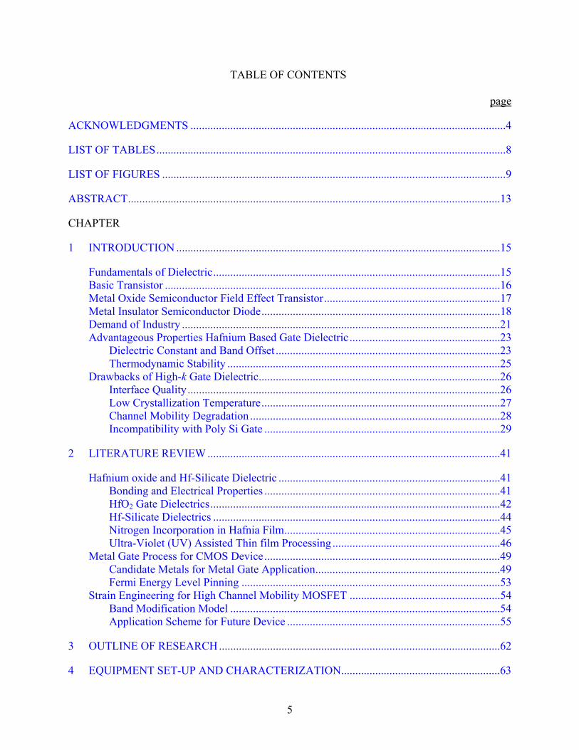
TABLE OF CONTENTS
page
ACKNOWLEDGMENTS ...............................................................................................................4
LIST OF TABLES...........................................................................................................................8
LIST OF FIGURES .........................................................................................................................9
ABSTRACT...................................................................................................................................13
CHAPTER
1 INTRODUCTION ..................................................................................................................15
Fundamentals of Dielectric.....................................................................................................15
Basic Transistor ......................................................................................................................16
Metal Oxide Semiconductor Field Effect Transistor..............................................................17
Metal Insulator Semiconductor Diode....................................................................................18
Demand of Industry ................................................................................................................21
Advantageous Properties Hafnium Based Gate Dielectric .....................................................23
Dielectric Constant and Band Offset ...............................................................................23
Thermodynamic Stability ................................................................................................25
Drawbacks of High-k Gate Dielectric.....................................................................................26
Interface Quality..............................................................................................................26
Low Crystallization Temperature....................................................................................27
Channel Mobility Degradation ........................................................................................28
Incompatibility with Poly Si Gate ...................................................................................29
2 LITERATURE REVIEW .......................................................................................................41
Hafnium oxide and Hf-Silicate Dielectric ..............................................................................41
Bonding and Electrical Properties ...................................................................................41
HfO2 Gate Dielectrics......................................................................................................42
Hf-Silicate Dielectrics .....................................................................................................44
Nitrogen Incorporation in Hafnia Film............................................................................45
Ultra-Violet (UV) Assisted Thin film Processing ...........................................................46
Metal Gate Process for CMOS Device...................................................................................49
Candidate Metals for Metal Gate Application.................................................................49
Fermi Energy Level Pinning ...........................................................................................53
Strain Engineering for High Channel Mobility MOSFET .....................................................54
Band Modification Model ...............................................................................................54
Application Scheme for Future Device ...........................................................................55
3 OUTLINE OF RESEARCH...................................................................................................62
4 EQUIPMENT SET-UP AND CHARACTERIZATION........................................................63
5
Laser System...........................................................................................................................63
Pulsed Laser Ablation via Excimer Lasers.............................................................................65
Vacuum Chamber, Component and Operation.......................................................................66
Atomic Layer Deposition .......................................................................................................67
Atomic Layer Deposition Process ...................................................................................67
Wafer Bending Experiment ....................................................................................................69
Material and Chemical Characterization Techniques.............................................................70
X-ray Reflectivity............................................................................................................70
X-ray Photoelectron Spectroscopy (XPS) .......................................................................71
High Resolution Transmission Electron Microscopy (HR-TEM)...................................72
Auger Electron Spectroscopy (AES)...............................................................................72
Secondary Ion Mass Spectroscopy (SIMS).....................................................................73
Electrical Characterization......................................................................................................74
Current-Voltage Measurements.......................................................................................75
Capacitance-Voltage Measurements ...............................................................................76
5 STUDY OF INTERFACE DEGRADATION OF HAFNIUM-SILICATE DIELECTRICS DURING THERMAL NITRIDATION PROCESS.....................................85
Introduction.............................................................................................................................85
Experimental Detail ................................................................................................................86
Results and Discussion ...........................................................................................................87
Conclusions.............................................................................................................................92
6 HIGH EFFICIENCY NITROGEN INCORPORATION TECHNIQUE USING UV ASSISTED LOW TEMPERATURE PROCESS FOR HAFNIA DIELECTRICS................99
Introduction.............................................................................................................................99
Experimental Detail ..............................................................................................................100
Results and Discussion .........................................................................................................101
Conclusion ............................................................................................................................104
7 UV ASSISTED LOW TEMPERATURE NITRIDATION AND POST DEPOSITION OXIDATION TECHNIQUE FOR HfO2 GATE DIELECTRIC..........................................110
Introduction...........................................................................................................................110
Experimental Detail ..............................................................................................................111
Results and Discussion .........................................................................................................112
UV Assisted Low Temperature Growth of Hafnia Film ...............................................112
UV Assisted Oxidation Resistance of Hafnia Film.......................................................115
Conclusions...........................................................................................................................117
8 AN EVALUATION OF COMPATIBILITY FOR TITANIM BASED METAL GATE ELECTRODE ON HAFNIUM-SILICATE DIELECTRICS FOR DUAL METAL GATE APPLICATIONS ......................................................................................................124
Introduction...........................................................................................................................124
Experimental Detail ..............................................................................................................125
6
Results and Discussions........................................................................................................126
Conclusions...........................................................................................................................129
9 AN EVALUATION OF THERMAL STABILITY OF TITANIUM BORIDE METAL GATE ON HF-SILICATE FOR P-CHANNEL METAL OXIDE SEMICONDUCTOR APPLICATION ....................................................................................................................134
Introduction...........................................................................................................................134
Experimental Detail ..............................................................................................................135
Results and Discussion .........................................................................................................136
Conclusions...........................................................................................................................139
10 STRAIN INDUCED CHANGES IN GATE LEAKAGE CURRENT AND DIELECTRIC CONSTANT OF NITRIDED HF-SILICATE DIELECTRIC SILICON MOS CAPACITORS............................................................................................................144
Introduction...........................................................................................................................144
Experimental Detail ..............................................................................................................145
Result and Discussion...........................................................................................................146
Conclusion ............................................................................................................................147
11 CONCLUSIONS ..................................................................................................................153
LIST OF REFERENCES.............................................................................................................155
BIOGRAPHICAL SKETCH .......................................................................................................164
7
LIST OF TABLES
Table page 1-1 The 2003 ITRS technology roadmap for memory device .................................................23
1-2 Gibbs free energy of formation for potential alternative high-k dielectrics ......................26
5-1 Summary of x-ray reflectivity data on roughness, density, and thickness of IL and HfSiNO films. ....................................................................................................................93
6-1 Summary of x-ray reflectivity data on roughness, density, and thickness of IL and Hf-silicate films. ..............................................................................................................107
8
LIST OF FIGURES
Figure page 1-1 Schematics of a typical MOSFET device. .........................................................................30
1-2 Schematics of MIS device. ...............................................................................................30
1-3 Energy band diagrams of ideal MIS diodes at V=0 (a) n-type and (b) p-type..................31
semiconductor ....................................................................................................................31
1-4 Energy band diagrams for ideal MIS diode structure when the gate is biased. (a) Accumulation (b) Depletion and (c) Inversion ..................................................................32
1-5 C-V curve shift based on the gate bias due to the positive or negative charges (a) for p-type semiconductor.........................................................................................................33
1-6 Distortion or stretch out of the C-V curve due to the presence of interface trapped charges ...............................................................................................................................33
1-7 Various electron tunneling modes. In films with thicknesses greater ~ 50 Å, FN tunneling dominates and the mechanism shifts to direct tunneling in films thinner than 50 Å............................................................................................................................34
1-8 Expected leakage current density and leakage current operation limit with respect to the equivalent oxide thickness (EOT)................................................................................35
1-9 Band gap and dielectric constant for gate oxide candidate materials. ...............................36
1-10 Conduction and valence band offset of various gate oxide candidate materials. ..............37
1-11 Comparison of GIXD of hafnium oxide film deposited at 200 oC and 600 oC .................37
1-12 Various scattering centers of MOSFET.............................................................................38
1-13 Comparison of channel mobility of SiO2 and higk-k dielectric MOSFET .......................39
1-14 Defect formation at the poly-Si and high-k dielectric interface is most likely the cause of the Fermi level pinning which causes high threshold voltages in MOSFET (M = Zr or Hf)....................................................................................................................40
2-1 Plot of work function versus atomic number. Work functions are generally observed to increasing moving across a row of transition metal elements. ......................................58
2-2 Process flow for the stacked dual metal gate integration. The difficulty in this approach is that two gate stacks of different heights need to be etched simultaneously.............................................................................................................................................59
9
2-3 Process flow for the metallic integration showing how two metals are formed by depositing a metal stack, selectively patterning and etching the top metal, and annealing to alloy the bi-metal stack. ................................................................................59
2-4 Process flow for the ion implantation and solid-state diffusion of nitrogen to form a nitrogen-rich (NMOS) and a nitrogen-deficient electrode (PMOS). .................................60
2-5 The six-fold degeneracy of electron, before and after biaxially tensile strain...................60
2-6 Schematic features of the various process strain: (a) silicon nitride capping layer to create a tensile channel (b) embedded SiGe S/D process strain to create a compressive strain..............................................................................................................61
4-1 Sketch of the pulsed laser deposition (PLD) system. ........................................................78
4-2 Photograph of an UV lamp array in the pulsed laser deposition system. The lamps were located at a distance of ~ 5-7 cm from the substrate.................................................78
4-3 Atomic layer deposition of ZrO2........................................................................................79
4-4 ALD acceptable temperature window ...............................................................................79
4-5 Schematic illustration of ALD HfSiOx deposition cycle. ................................................80
4-6 A fixture to simulate uniaxially-strained MOS devices. For a uniaxial stress, two pairs of cylindrical rods are used and a sample is inserted between the pairs. ..................81
4-7 Illustration of a uniaxial wafer bending jig. (a) an unstressed sample (b) a stressed sample. (c) is the practical deflection and induced stress. .................................................82
4-8 Typical X-ray reflectivity (XRR) spectrum from a thin film deposited on Si...................83
4-9 Typical X-ray photoelectron spectroscopy spectrum of graded hafnium silicate film deposited on silicon. The binding energy shifts of Hf 4f photoelectron peak can be used to determine the nature of bonding present in the films. The different angles represent the photoelectron take off angles or escape angles. ...........................................83
4-10 Metal oxide semiconductor capacitance-voltage curves (a) low frequency (b) high frequency and (c) deep depletion.......................................................................................84
5-1 The comparison of XRR patterns with respect to the nitridation temperature. .................93
5-2 Dependence of (a) Hf 4f peak region and (b) N 1s core level of XPS scan on nitridation temperature. The percentages in N 1s deconvoluted spectra represent area fraction of the respective peaks..........................................................................................94
5-3 Electrical measurement results of Pt/Hf-silicate/Si MOS device fabricated on films with different nitridation treatments (a) Flat band voltage and (b) current density – gate voltage characteristic..................................................................................................95
10
5-4 Cumulative probability of breakdown voltage for 7 nm thick Hf-silicate on Pt electrode with respect to the nitridation temperature. Lines are fits to a Weibull distribution (Eq. 5-1)..........................................................................................................96
5-5 Interface state density (Dit) changes with respect to the nitridation temperature. ............97
5-6 (a ) The change of peak electron mobility with respect to the nitridation temperatures (b) Electron mobility versus electric field in MOSFET device fabricated for HfSiON films of 1.2 nm EOT (poly Si gate) nitrided at 650 oC and 850 o C................................................................................................................................98
6-1 XPS Si 2p spectra comparison of Hf-silicate films with respect to the methodological approaches (350 °C thermally nitrided sample 1, 650 °C thermally nitrided sample 2, and 350 °C UV nitrided sample 3)...................................................................................106
6-2 X-ray reflectivity (XRR) scans of thermally nitrided (samples 1 and 2) and UV nitrided (sample 3) films..................................................................................................107
6-3 SIMS depth profile of thermally nitrided film (650 °C) and UV nitrided film ...............108
(350 °C) after 400 °C UV oxidation (a) oxygen and (b) nitrogen. ..................................108
6-4 C-V comparison plot of three set of samples with 400 °C UV oxidation. .......................109
7-1 XPS Si 2p spectra comparison of nitrided samples (sample 1 and 2) and non-nitrided sample 3. ..........................................................................................................................119
7-2 Cross-sectional HR-TEM images. (a) non-nitrided sample 3 (b) UV assisted nitrided sample 1. ..........................................................................................................................120
7-3 Comparison of electrical properties of nitrided samples and non-nitrided sample (a) C-V comparison (b) J-V comparison................................................................................120
7-4 The interfacial layer thickness changes with respect to the PDA times for sample 1 and 3.................................................................................................................................121
7-5 The interfacial layer density changes with respect to the PDA times for sample 1 and 3........................................................................................................................................122
7-6 XPS Si 2p spectra comparison with respect to the PDA times (a) UV assisted nitrided sample 1 (b) non-nitrided sample 3. ...................................................................122
7-7 Arrhenius plots for interfacial growth for UV assisted nitrogen incorporated films and vacuum deposited films(a). Comparison of activation energies for oxygen diffusion in various oxidation times for sample 1 and 3(b). ............................................123
8-1 C-V characteristics of the MOS device with Ti, TiN, and TiB2 gate on Hf-silicate film at 1 MHz...................................................................................................................130
11
8-2 The (qVfb + Φsub) vs EOT plots for the Ti, TiN and TiB2 gates. The EOTi and dielectric constant were determined by EOT vs Thigh-k plot inset in figure......................131
8-3 J-V plot for Ti, TiN and TiB2 gates on Hf-silicate dielectric. Inset in figure shows Poole-Frenkel (ln(J/E) vs E1/2) plot of three kinds of Ti based electrodes on Hf-silicate at 25 oC.................................................................................................................132
8-4 Extracted trap depth of MOS devices with three kinds of gate electrode using slope of ln(J/E) vs 1/T plot at different gate voltage which were inset in the figure. ...............133
9-1 Electrical measurement results (a) C-V characteristics at 1MHz of the MOS device with TiB2 gate on Hf-silicate film with at different annealing temperatures, (b) The qVfb + Φsub vs EOT plots for the TiB2 gate after different annealing. Φmeff with consideration of interface is inset in figure......................................................................140
9-2 AES depth profiles of Au/Ti/TiB2/Hf-silicate/Si MOS structure as a function of annealing temperature......................................................................................................141
9-3 HRTEM images of TiB2/ Hf-silicate (7 nm)/Si stack at as-deposited state and after annealing at 1100 °C under N2 atmosphere. ....................................................................142
9-4 Electrical measurement results (a) EOT vs leakage current density plot at 1MV/cm for TiB2 gates on Hf-silicate dielectric of different annealing temperatures. Inset figure is hysteresis (ΔVH) of TiB2/Hf-silicate/Si MOS capacitors as a function of annealing temperature......................................................................................................143
10-1 C-V characteristics at 1MHz of the MOS device with Pt and Al gate on nitrided Hf-silicate film. The inset shows current density-voltage (J-V) measurements of both devices..............................................................................................................................149
10-2 Poole-Frenkel (ln(J/E) vs E1/2) plot of Pt and Al gate on nitrided Hf-silicate film at 25 oC. Inset in figure shows a schematic band diagram for MOS capacitors with HfSiON dielectric and interlayer and metal gates (Pt and Al) under negative gate bias...........................................................................................................................................150
10-3 Changes in gate leakage current of Si MOS capacitors with HfSiON dielectric as a function of applied stress. ................................................................................................151
10-4 Changes in dielectric constant of HfSiON, HfSiOx and HfO2, measured from C-V and PF slope change.........................................................................................................152
12
Abstract of Dissertation Presented to the Graduate School of the University of Florida in Partial Fulfillment of the Requirements for the Degree of Doctor of Philosophy
NITROGEN INCORPORATED HAFNIA GATE DIELECTRIC THIN FILM AND TITANIUM
BASED METAL GATE ELECTRODE FOR DUAL GATE APPLICATION
By
Seung-young Son
August 2008 Chair: Rajiv K. Singh Major: Materials Science and Engineering
We evaluated the effect of nitridation temperature on interface layer (IL) quality of Hf-
silicate gate dielectric has been reported. An increase in IL density and IL roughness was
observed as the nitridation temperature was increased. Preferential interface reaction at
dielectric-Si interface at higher temperatures was analyzed. The progressive increase in IL
roughness finally led to degradation of breakdown voltage, shift in flat band voltage (0.54V) and
deterioration of electron channel mobility by 20 % in samples nitrided at 1123 K. To reduce the
interface degradation of thermal nitridation process, a low temperature process (623 K) for
nitrogen incorporation in hafnia gate dielectric has been proposed. This method is based on post-
deposition nitridation under ultraviolet light illuminated NH3 ambience. Uniformity of nitrogen
distribution in the film was measured. Moreover, the amount of nitrogen incorporated by this
process was comparable to that of high temperature thermal nitridation, maintaining low
interface roughness (0.3 nm).
An evaluation of Ti based gate metals has been reported. The effective metal work
function were 4.27, 4.56 and 5.08 eV for Ti, TiN and TiB2, respectively. Regardless of gate
electrodes, the conduction mechanism of the samples fitted with Poole-Frenkel model which is
related to oxygen vacancies in the film. Ti gate electrode was found to be more favorable for
13
14
NMOS device and TiB2 gate electrode can be used for PMOS. Further research for thermal
stability of TiB2 gate electrodes was conducted. The extracted effective metal work function for
TiB2 gate was about 5.08 eV. The work function showed almost identical values and sharp
interface between metal and dielectric was confirmed after post deposition annealing by 1273 K.
The work function lowering (4.91 eV) at 1373 K was caused by metal-dielectric intermixing and
oxygen vacancy formation. TiB2 gate electrode was found to be suitable for use in PMOS device.
Finally, Uniaxial–mechanical–strain altered gate leakage current and dielectric constant of
MOS device are measured. Uniaxial stress is applied using four–point wafer bending along one
one zero plane direction. The gate leakage current and dielectric constant are found to increase
by up to 2 % under tensile and compressive stress direction.
CHAPTER 1 INTRODUCTION
Fundamentals of Dielectric
Dielectrics are a class of materials, which have no free carriers for electrical conduction.
They are also known as insulators (non-metallic) and exhibit or can be made to exhibit a dipole
structure. A dipole refers to the separation of positively and negatively charged entities on an
atomic level. These charged entities are bound to the atom or molecule and are therefore not
available for conduction. When dielectric materials are placed in an electric field, a phenomenon
called “polarization” occurs whereby there is a shift in the charge distribution that leads to the
dielectric behavior of the material system.1 Polarization induces electric dipoles, which are
aligned with the applied field. The resistance of a material to polarization is measured by a
parameter called the dielectric constant (k). Dielectric materials are widely used in modern
electronics. Passivation of high voltage junctions, isolation of devices and interconnects, gate
insulation in field effect transistors are a few of the applications which involve dielectric
materials. Silicon dioxide (SiO2), silicon nitride (Si3N4) and aluminum oxide (Al2O3) are a few of
the commonly used dielectric materials in different areas of electronics and technology.
The dielectric constant is the ratio of the permittivity of the material (ε) to the permittivity
of vacuum or free space (εo).
κ = ε / ε o (1-1)
When two metal plates (parallel plate capacitor structure) are placed under an electric field,
one plate becomes positively charged and the other becomes negatively charged. The
capacitance C is related to the magnitude of charge stored on either plate Q by
C = Q / V (1-2)
15
where V = voltage applied across the plates. The units of capacitance are farads (F) or
coulombs/volt. When vacuum is present in between the parallel plates, the capacitance is
computed by
C = ε 0 [A / L] (1-3)
where A = area of the plates L = distance between the plates ε0 = permittivity of free space
or vacuum (8.85 10-12 F/m) ×
If a dielectric material is inserted in between the two plates, then the capacitance is
computed by
C = ε [A / L] (1-4)
Where ε = permittivity of the dielectric material. ε is always greater than unity The ratio of
the permittivity of the dielectric material to the permittivity of free space or vacuum is termed as
the relative permittivity. It is denoted by
ε r = ε / ε o (1-5)
Relative permittivity is unitless and is also called as the dielectric constant of the material.
As it is greater than unity, insertion of a dielectric material between the two metal plates
represents an increase in charge storing capacity of the parallel plate capacitor.
Basic Transistor
The transistor is arguably one of the most important inventions of the twentieth century.
The invention of this device has created countless technological advancements in the field of
modern science and technology. Tremendous advancements based on the basic transistor have
now enabled transfer of data, information and ideas from one corner of the world to the other in a
matter a few seconds. In the current generation devices, the microprocessors (heart of a
computer) contain millions of transistors, which are meticulously and completely integrated onto
a small microchip. The basis of the current computer technology is the use of complementary
16
metal oxide semiconductor (CMOS) schemes as the logic components in integrated circuits
(IC’s). Vacuum tubes were initially used (before the invention of transistors) for signal
amplification purposes in the long distance communication devices. Though the state of art
technology then, the vacuum tubes came with a number of disadvantages. They were bulky,
required extensive cooling, and consumed enormous power for operation. Around the mid
1940’s research was being conducted at Bell Laboratories (popularly known as Bell Labs)
towards a new variety of materials called semiconductors. These are non-metals (Si and Ge),
which could be made conducting by the addition of minute amounts of impurities (dopants). The
first transistor was created on the 16th December 1947 and it consisted of strips of gold foil on a
plastic triangle in intimate contact with a slab of germanium (Ge). This design soon underwent
improvements with the creation of the junction “sandwich” transistor. The use of semiconductors
presented the scientific community with advantages such as no warm up time, less power
consumption and higher efficiency. Towards the end of the 1950’s, the transistor design was
modified (individually by Jack Kilby and Robert Noyce) into a simplified integrated circuit
(device which contained more than one transistor).
Metal Oxide Semiconductor Field Effect Transistor
The metal oxide field effect transistor (MOSFET) is one of the key components in an
electronic device, particularly in digital integrated circuits. In this device a voltage applied on a
contact called “gate,” which is isolated from a conducting channel by a dielectric, controls the
current flow through a conducting channel in the device. The transistor basically works as a
switching device based on the field effect theory. A schematic of a MOSFET is shown in Figure
1-1.2 The conducting channel could be n or p type. The substrate polarity is opposite of that of
the channel. For example, an n type channel is created in a p-type Si substrate. Holes and
electrons are the majority carriers responsible for current conduction in p-type and n-type silicon
17
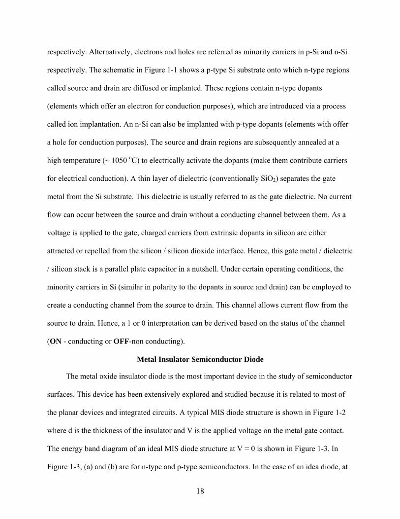
respectively. Alternatively, electrons and holes are referred as minority carriers in p-Si and n-Si
respectively. The schematic in Figure 1-1 shows a p-type Si substrate onto which n-type regions
called source and drain are diffused or implanted. These regions contain n-type dopants
(elements which offer an electron for conduction purposes), which are introduced via a process
called ion implantation. An n-Si can also be implanted with p-type dopants (elements with offer
a hole for conduction purposes). The source and drain regions are subsequently annealed at a
high temperature (~ 1050 oC) to electrically activate the dopants (make them contribute carriers
for electrical conduction). A thin layer of dielectric (conventionally SiO2) separates the gate
metal from the Si substrate. This dielectric is usually referred to as the gate dielectric. No current
flow can occur between the source and drain without a conducting channel between them. As a
voltage is applied to the gate, charged carriers from extrinsic dopants in silicon are either
attracted or repelled from the silicon / silicon dioxide interface. Hence, this gate metal / dielectric
/ silicon stack is a parallel plate capacitor in a nutshell. Under certain operating conditions, the
minority carriers in Si (similar in polarity to the dopants in source and drain) can be employed to
create a conducting channel from the source to drain. This channel allows current flow from the
source to drain. Hence, a 1 or 0 interpretation can be derived based on the status of the channel
(ON - conducting or OFF-non conducting).
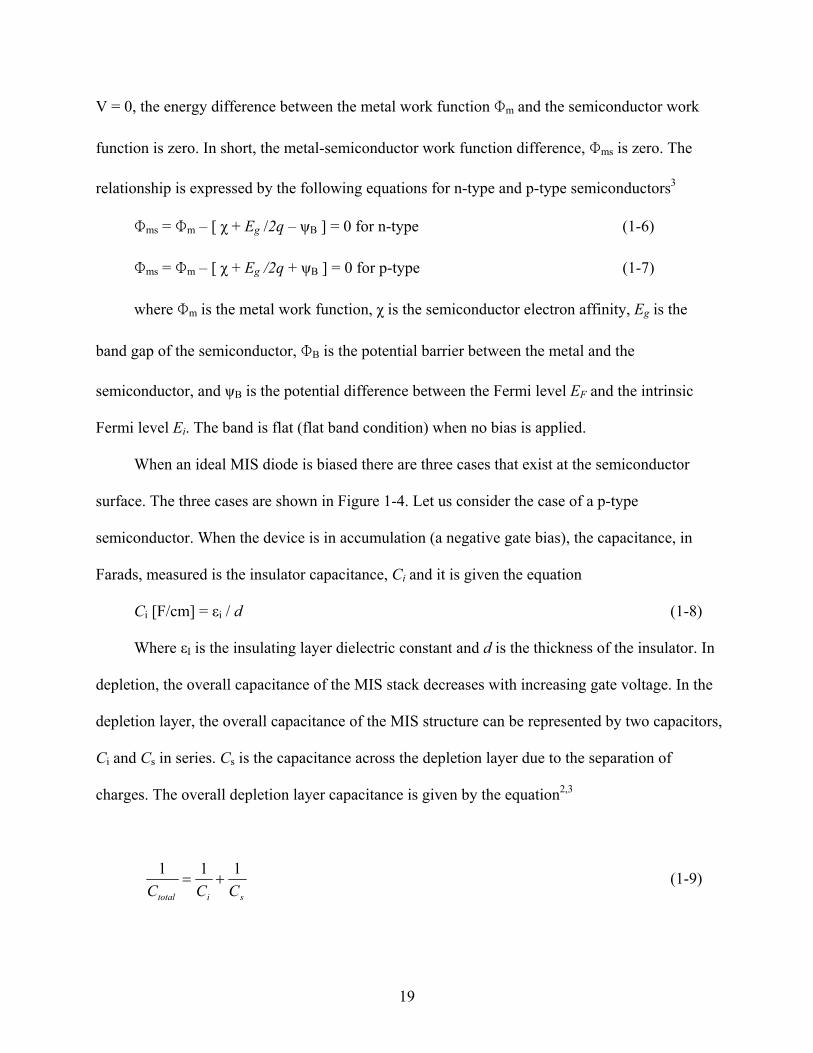
Metal Insulator Semiconductor Diode
The metal oxide insulator diode is the most important device in the study of semiconductor
surfaces. This device has been extensively explored and studied because it is related to most of
the planar devices and integrated circuits. A typical MIS diode structure is shown in Figure 1-2
where d is the thickness of the insulator and V is the applied voltage on the metal gate contact.
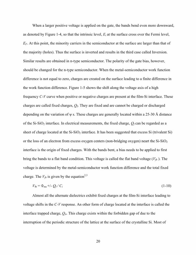
The energy band diagram of an ideal MIS diode structure at V = 0 is shown in Figure 1-3. In
Figure 1-3, (a) and (b) are for n-type and p-type semiconductors. In the case of an idea diode, at
18
V = 0, the energy difference between the metal work function Φm and the semiconductor work
function is zero. In short, the metal-semiconductor work function difference, Φms is zero. The
relationship is expressed by the following equations for n-type and p-type semiconductors3
Φms = Φm – [ χ + Eg /2q – ψB ] = 0 for n-type (1-6)
Φms = Φm – [ χ + Eg /2q + ψB ] = 0 for p-type (1-7)
where Φm is the metal work function, χ is the semiconductor electron affinity, Eg is the
band gap of the semiconductor, ΦB is the potential barrier between the metal and the
semiconductor, and ψB is the potential difference between the Fermi level EF and the intrinsic
Fermi level Ei. The band is flat (flat band condition) when no bias is applied.
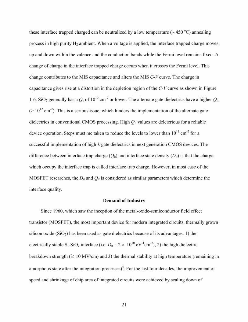
When an ideal MIS diode is biased there are three cases that exist at the semiconductor
surface. The three cases are shown in Figure 1-4. Let us consider the case of a p-type
semiconductor. When the device is in accumulation (a negative gate bias), the capacitance, in
Farads, measured is the insulator capacitance, Ci and it is given the equation
Ci [F/cm] = εi / d (1-8)
Where εI is the insulating layer dielectric constant and d is the thickness of the insulator. In
depletion, the overall capacitance of the MIS stack decreases with increasing gate voltage. In the
depletion layer, the overall capacitance of the MIS structure can be represented by two capacitors,
Ci and Cs in series. Cs is the capacitance across the depletion layer due to the separation of
charges. The overall depletion layer capacitance is given by the equation2,3
sitotal CCC
111+= (1-9)
19
When a larger positive voltage is applied on the gate, the bands bend even more downward,
as denoted by Figure 1-4, so that the intrinsic level, Ei at the surface cross over the Fermi level,
EF. At this point, the minority carriers in the semiconductor at the surface are larger than that of
the majority (holes). Thus the surface is inverted and results in the third case called Inversion.
Similar results are obtained in n-type semiconductor. The polarity of the gate bias, however,
should be changed for the n-type semiconductor. When the metal-semiconductor work function
difference is not equal to zero, charges are created on the surface leading to a finite difference in
the work function difference. Figure 1-5 shows the shift along the voltage axis of a high
frequency C-V curve when positive or negative charges are present at the film-Si interface. These
charges are called fixed charges, Qf. They are fixed and are cannot be charged or discharged
depending on the variation of ψ s. These charges are generally located within a 25-30 Å distance
of the Si-SiO2 interface. In electrical measurements, the fixed charge, Qf can be regarded as a
sheet of charge located at the Si-SiO2 interface. It has been suggested that excess Si (trivalent Si)
or the loss of an electron from excess oxygen centers (non-bridging oxygen) neart the Si-SiO2
interface is the origin of fixed charges. With the bands bent, a bias needs to be applied to first
bring the bands to a flat band condition. This voltage is called the flat band voltage (Vfb ). The
voltage is determined by the metal-semiconductor work function difference and the total fixed
charge. The Vfb is given by the equation2,3
Vfb = Φms +/- Qf / Ci (1-10)
Almost all the alternate dielectrics exhibit fixed charges at the film-Si interface leading to
voltage shifts in the C-V response. An other form of charge located at the interface is called the
interface trapped charge, Qit. This charge exists within the forbidden gap of due to the
interruption of the periodic structure of the lattice at the surface of the crystalline Si. Most of
20
these interface trapped charged can be neutralized by a low temperature (~ 450 oC) annealing
process in high purity H2 ambient. When a voltage is applied, the interface trapped charge moves
up and down within the valence and the conduction bands while the Fermi level remains fixed. A
change of charge in the interface trapped charge occurs when it crosses the Fermi level. This
change contributes to the MIS capacitance and alters the MIS C-V curve. The charge in
capacitance gives rise at a distortion in the depletion region of the C-V curve as shown in Figure
1-6. SiO2 generally has a Qit of 1010 cm-2 or lower. The alternate gate dielectrics have a higher Qit
(> 1012 cm-2). This is a serious issue, which hinders the implementation of the alternate gate
dielectrics in conventional CMOS processing. High Qit values are deleterious for a reliable
device operation. Steps must me taken to reduce the levels to lower than 1011 cm-2 for a
successful implementation of high-k gate dielectrics in next generation CMOS devices. The
difference between interface trap charge (Qit) and interface state density (Dit) is that the charge
which occupy the interface trap is called interface trap charge. However, in most case of the
MOSFET researches, the Dit and Qit is considered as similar parameters which determine the
interface quality.
Demand of Industry
Since 1960, which saw the inception of the metal-oxide-semiconductor field effect
transistor (MOSFET), the most important device for modern integrated circuits, thermally grown
silicon oxide (SiO2) has been used as gate dielectrics because of its advantages: 1) the
electrically stable Si-SiO2 interface (i.e. Dit ~ 2 × 10¹⁰ eV-1cm-2), 2) the high dielectric
breakdown strength (≥ 10 MV/cm) and 3) the thermal stability at high temperature (remaining in
amorphous state after the integration processes)4. For the last four decades, the improvement of
speed and shrinkage of chip area of integrated circuits were achieved by scaling down of
21
physical thickness of the SiO2 gate dielectrics and gate length (L). However, beyond the 100 nm
node technology, SiO2 has reached its physical limitations: higher leakage current and reliability
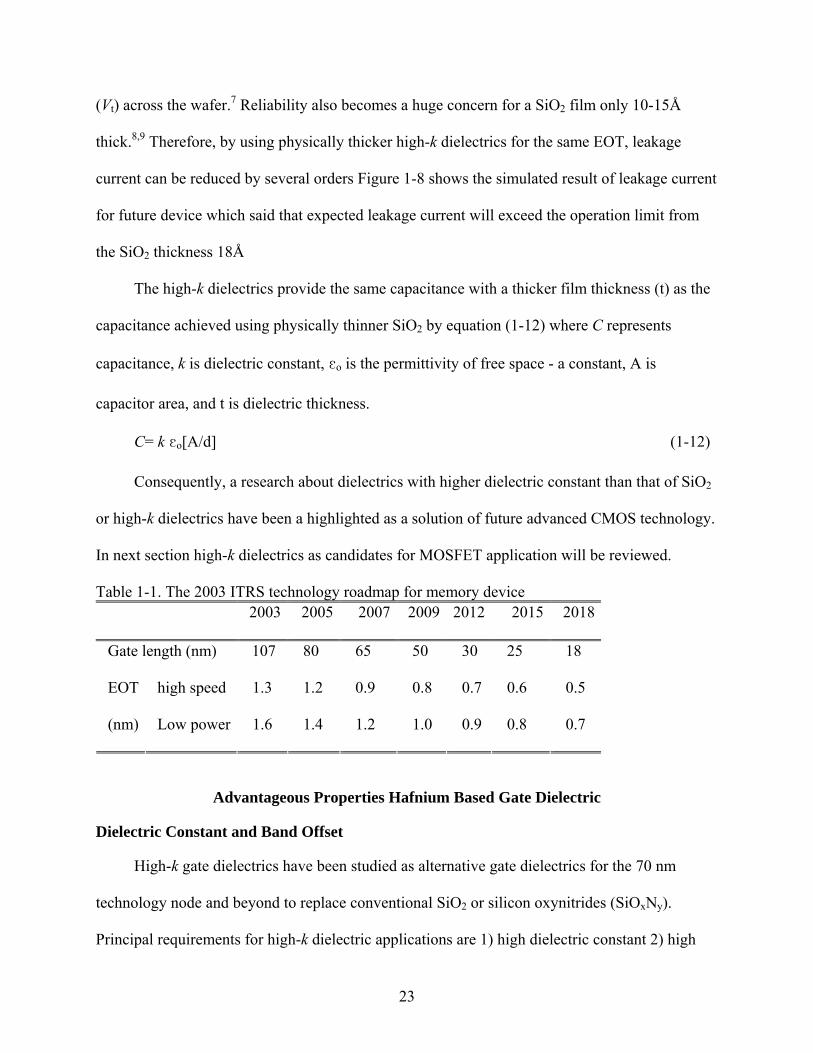
concerns. As shown in Table 1-1,5 continuing scaling down of the MOSFET device with the
minimum feature size of 90 nm and below requires EOT (Equivalent Oxide Thickness) less than
15 Å. A 10-15Å-thick SiO2 layer corresponds to only around 3-4 mono-layers of SiO2. In this
thinner EOT range, SiO2 suffers from leakage current too high to be used (particularly) for low
power operation due to the direct tunneling of electrons as shown Fig. 1-7. 2,6
Leakage current of SiO2 is governed by Fouler-Nordheim tunneling where conduction
occurs by field assisted electron tunneling at the field range of Vi ≡ Ei d > ΦB while direct
tunneling of electrons at the lower field Vi ≡ Ei d < φB where Vi , Ei , and ΦB represent voltage
applied to dielectric, electric field across dielectric and barriers height between gate electrode
and dielectric, respectively.2 In other words, as the thickness of SiO2 becomes thinner, leakage
current is more likely to be governed by direct tunneling current which increases significantly as
thickness becomes thinner by equation (1-11).
⎪⎭
⎪⎬⎫
⎪⎩
⎪⎨⎧
⎟⎟⎠
⎞⎜⎜⎝
⎛−Φ−⎟
⎠⎞
⎜⎝⎛ +Φ−⎟⎟
⎠
⎞⎜⎜⎝
⎛−Φ−⎟
⎠⎞
⎜⎝⎛ −Φ=
2exp
22exp
22
VBdVVBdVdAJ BBBB (1-11)
Where h
qAπ2
2
= , h
qmB
*24π= and BΦ is barrier height, respectively. In equation (1-11)
q, m*, and h represent electron charge, effective mass of electron, and Plank’s constant,
respectively.
In addition, SiO2 thickness uniformity across a 12 inch wafer imposes even more crucial
difficulty in the growth of such a thin film, since even a mono-layer difference in thickness
represents a large percentage difference and thus can result in the variation of threshold voltage
22
(Vt) across the wafer.7 Reliability also becomes a huge concern for a SiO2 film only 10-15Å
thick.8,9 Therefore, by using physically thicker high-k dielectrics for the same EOT, leakage
current can be reduced by several orders Figure 1-8 shows the simulated result of leakage current
for future device which said that expected leakage current will exceed the operation limit from
the SiO2 thickness 18Å
The high-k dielectrics provide the same capacitance with a thicker film thickness (t) as the
capacitance achieved using physically thinner SiO2 by equation (1-12) where C represents
capacitance, k is dielectric constant, εo is the permittivity of free space - a constant, A is
capacitor area, and t is dielectric thickness.
C= k εo[A/d] (1-12)
Consequently, a research about dielectrics with higher dielectric constant than that of SiO2
or high-k dielectrics have been a highlighted as a solution of future advanced CMOS technology.
In next section high-k dielectrics as candidates for MOSFET application will be reviewed.
Table 1-1. The 2003 ITRS technology roadmap for memory device 2003 2005 2007 2009 2012 2015 2018
Gate length (nm) 107 80 65 50 30 25 18
high speed 1.3 1.2 0.9 0.8 0.7 0.6 0.5 EOT
(nm) Low power 1.6 1.4 1.2 1.0 0.9 0.8 0.7
Advantageous Properties Hafnium Based Gate Dielectric
Dielectric Constant and Band Offset
High-k gate dielectrics have been studied as alternative gate dielectrics for the 70 nm
technology node and beyond to replace conventional SiO2 or silicon oxynitrides (SiOxNy).
Principal requirements for high-k dielectric applications are 1) high dielectric constant 2) high
23
band offset with electrodes (i.e. barrier height) to suppress leakage current 3) thermally and
chemically stable in contact with Si substrate.
In Figure 1-9, dielectric constants of high-k candidates were summarized. A TiO2 showing
profoundly higher k in Figure 1-9, was reported not to be thermally stable with silicon
substrates.10 Moreover, it is worth mentioning that high-k dielectrics such as BST with a too high
dielectric constant ( >100) does not seem to be appropriate since the excessive high dielectric
constant causes field induced barrier lowering (FIBL) which degrade short channel effects of
MOSFETs.11
For electrons traveling from the Si substrate to the gate, the conduction band offset (ΔEc)
is the barrier and for electrons traveling from the gate to the Si substrate. A favorable band
alignment is very essential because the leakage current increases exponentially with decreasing
barrier height and thickness for direct electron tunneling transport mechanism. Figure 1-10
shows the relative band alignment of various prospective material systems with Si. If the
experimental ΔEc values of these systems were much less than 1.0 eV, electron transport would
lead to unacceptable leakage current precluding the implementation of a particular material
system. Since most of the new systems do not have reported values of ΔEc, the band gap (Eg) is
commonly used as an indication of the possible values of ΔEc. However, the valence and
conduction band offsets need not always be symmetric as in some material systems, the valence
band offsets constitute most of the band gap. Hence, the prospective material of choice should
posses a favorable band offset as well as a higher band gap.
A Ta2O5, which has been studied widely for the application in DRAM storage capacitors
appears to be inappropriate for the gate electrode application. Also, the Al2O3 and Si3N4 which
show reasonable band offsets, can not satisfy the dielectric constant criteria as shown in
24
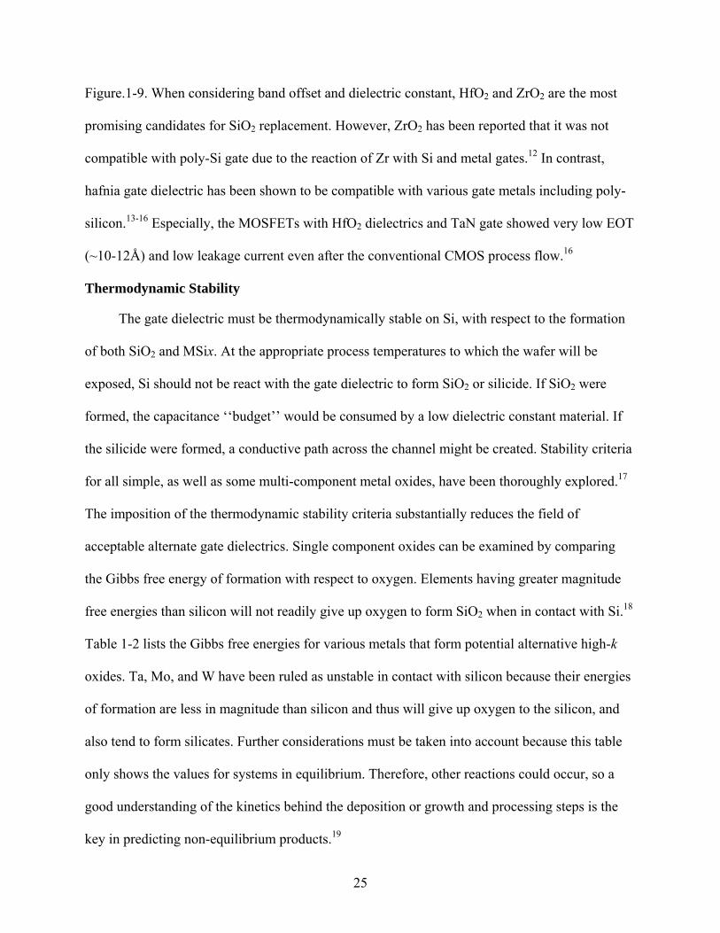
Figure.1-9. When considering band offset and dielectric constant, HfO2 and ZrO2 are the most
promising candidates for SiO2 replacement. However, ZrO2 has been reported that it was not
compatible with poly-Si gate due to the reaction of Zr with Si and metal gates.12 In contrast,
hafnia gate dielectric has been shown to be compatible with various gate metals including poly-
silicon.13-16 Especially, the MOSFETs with HfO2 dielectrics and TaN gate showed very low EOT
(~10-12Å) and low leakage current even after the conventional CMOS process flow.16
Thermodynamic Stability
The gate dielectric must be thermodynamically stable on Si, with respect to the formation
of both SiO2 and MSix. At the appropriate process temperatures to which the wafer will be
exposed, Si should not be react with the gate dielectric to form SiO2 or silicide. If SiO2 were
formed, the capacitance ‘‘budget’’ would be consumed by a low dielectric constant material. If
the silicide were formed, a conductive path across the channel might be created. Stability criteria
for all simple, as well as some multi-component metal oxides, have been thoroughly explored.17
The imposition of the thermodynamic stability criteria substantially reduces the field of
acceptable alternate gate dielectrics. Single component oxides can be examined by comparing
the Gibbs free energy of formation with respect to oxygen. Elements having greater magnitude
free energies than silicon will not readily give up oxygen to form SiO2 when in contact with Si.18
Table 1-2 lists the Gibbs free energies for various metals that form potential alternative high-k
oxides. Ta, Mo, and W have been ruled as unstable in contact with silicon because their energies
of formation are less in magnitude than silicon and thus will give up oxygen to the silicon, and
also tend to form silicates. Further considerations must be taken into account because this table
only shows the values for systems in equilibrium. Therefore, other reactions could occur, so a
good understanding of the kinetics behind the deposition or growth and processing steps is the
key in predicting non-equilibrium products.19
25
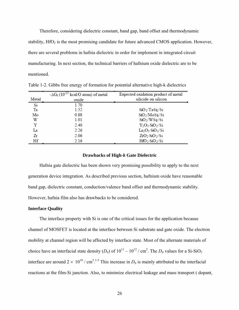
Therefore, considering dielectric constant, band gap, band offset and thermodynamic
stability, HfO2 is the most promising candidate for future advanced CMOS application. However,
there are several problems in hafnia dielectric in order for implement in integrated circuit
manufacturing. In next section, the technical barriers of hafnium oxide dielectric are to be
mentioned.
Table 1-2. Gibbs free energy of formation for potential alternative high-k dielectrics
Drawbacks of High-k Gate Dielectric
Hafnia gate dielectric has been shown very promising possibility to apply to the next
generation device integration. As described previous section, hafnium oxide have reasonable
band gap, dielectric constant, conduction/valence band offset and thermodynamic stability.
However, hafnia film also has drawbacks to be considered.
Interface Quality
The interface property with Si is one of the critical issues for the application because
channel of MOSFET is located at the interface between Si substrate and gate oxide. The electron
mobility at channel region will be affected by interface state. Most of the alternate materials of
choice have an interfacial state density (Dit) of 1011 – 1012 / cm2. The Dit values for a Si-SiO2
interface are around 2 1010 / cm2.1-5 This increase in Dit is mainly attributed to the interfacial
reactions at the film-Si junction. Also, to minimize electrical leakage and mass transport ( dopant,
×
26
Si etc), the interfacial layer should be amorphous phase because the grain boundary of poly-
crystalline interface could be an inappropriate path. Hence, interface engineering schemes have
been developed to form oxynitrides and oxide/nitride reaction barriers between these high-k
metal oxide materials and Si in an attempt to prevent or at least minimize reaction with the
underlying Si.20-25 These barrier layers have been shown to reduce the extent of reaction between
the high-k dielectric and Si, as well as to help maintain a high channel carrier mobility. It is
important to note, however, that using an interfacial layer of SiO2 or another low permittivity
material, will limit the highest possible gate stack capacitance, or equivalently, the lowest
achievable EOT value.
Moreover, several simple oxides including HfO2 have been reported as having high oxygen
diffusivity. Any annealing treatments which have an excess of oxygen present (either from the
ambient or from a sidewall oxide, for example) will lead to rapid oxygen diffusion through the
oxides, resulting in SiOx or SiO2-containing interface layers. Since this oxide layer is completely
uncontrollable and unexpected layer, the quality of interface can not be same as intentionally
thermal grown SiO2 film. It is important to note that using an interfacial layer of SiO2 or another
low permittivity material, will limit the highest possible gate stack capacitance, or equivalently,
the lowest achievable EOT value
Low Crystallization Temperature
The most serious problem of hafnium oxide is known as low crystallization temperature.
Generally, the device integration process includes high temperature ( < 1000 oC) process for
example carrier activation annealing after ion implantation, metal filling on high aspect ratio
contact, RTA and etc. Therefore, the gate oxide heat budget can not be avoidable. During the
integration process, amorphous hafnium oxide films are easily crystallized under 600 oC and then
changed to a partially crystallized poly crystalline hafnium oxide film. As the grain boundary of
27
poly crystalline oxide will be a large current path and mass transportation source, the low
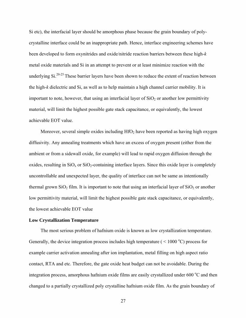
crystallization temperature is a critical barrier to be overcome. Figure 1-11 shows the comparison
of grazing incidence x-ray diffraction (GIXD) of hafnium oxide films which were deposited at
200 oC and 600 oC. The sample in the 200°C deposition remained amorphous which is to be
expected as the crystallization temperature for HfO2 is 450-500 °C. However, the 600 oC
deposited film at exhibited broad peaks, a sign of rather poor and randomly oriented crystallites.
Identification of the main peaks and relative intensities was found to match the monoclinic HfO2
phase The peak at 55.5° is from the (311) plane of the silicon substrate.
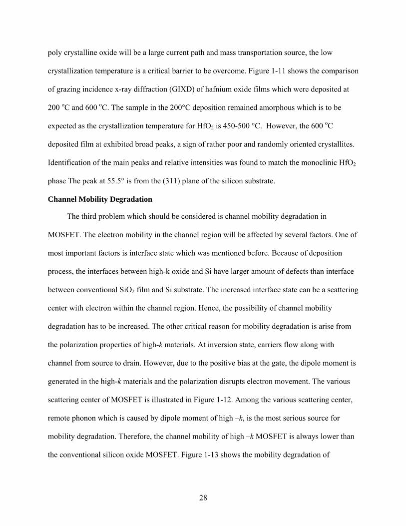
Channel Mobility Degradation
The third problem which should be considered is channel mobility degradation in
MOSFET. The electron mobility in the channel region will be affected by several factors. One of
most important factors is interface state which was mentioned before. Because of deposition
process, the interfaces between high-k oxide and Si have larger amount of defects than interface
between conventional SiO2 film and Si substrate. The increased interface state can be a scattering
center with electron within the channel region. Hence, the possibility of channel mobility
degradation has to be increased. The other critical reason for mobility degradation is arise from
the polarization properties of high-k materials. At inversion state, carriers flow along with
channel from source to drain. However, due to the positive bias at the gate, the dipole moment is
generated in the high-k materials and the polarization disrupts electron movement. The various
scattering center of MOSFET is illustrated in Figure 1-12. Among the various scattering center,
remote phonon which is caused by dipole moment of high –k, is the most serious source for
mobility degradation. Therefore, the channel mobility of high –k MOSFET is always lower than
the conventional silicon oxide MOSFET. Figure 1-13 shows the mobility degradation of
28
MOSFET using SiO2 gate and high-k dielectric. The channel mobility of high-k device is around
40% lower than SiO2 gate due to the increased polarization and remote phonon scattering.26-29
Incompatibility with Poly Si Gate
The final technological barrier of high-k dielectric application is incompatibility with poly-
Si gate material. The conventional CMOS technologies have used poly-Si gate materials due to
the relatively easy process and good compatibility with SiO2/SiON gate dielectrics. Thus, the
huge amounts of integration knowledge have been accumulated based on the poly-Si gate. The
main advantages of poly-Si gate are listed below.
• Compatible with high temperature process : self-aligned source & drain (SAC process)
• Work function can be tuned via doping control : easy approach to dual gate scheme
• Easy to deposit : LPCVD minimal damage and good step coverage
• Easy to etch and good removal by CMP : poly-Si can be etched (having high selectivity with SiO2 and nitride) using SF6, NF3, Cl2 chemistry
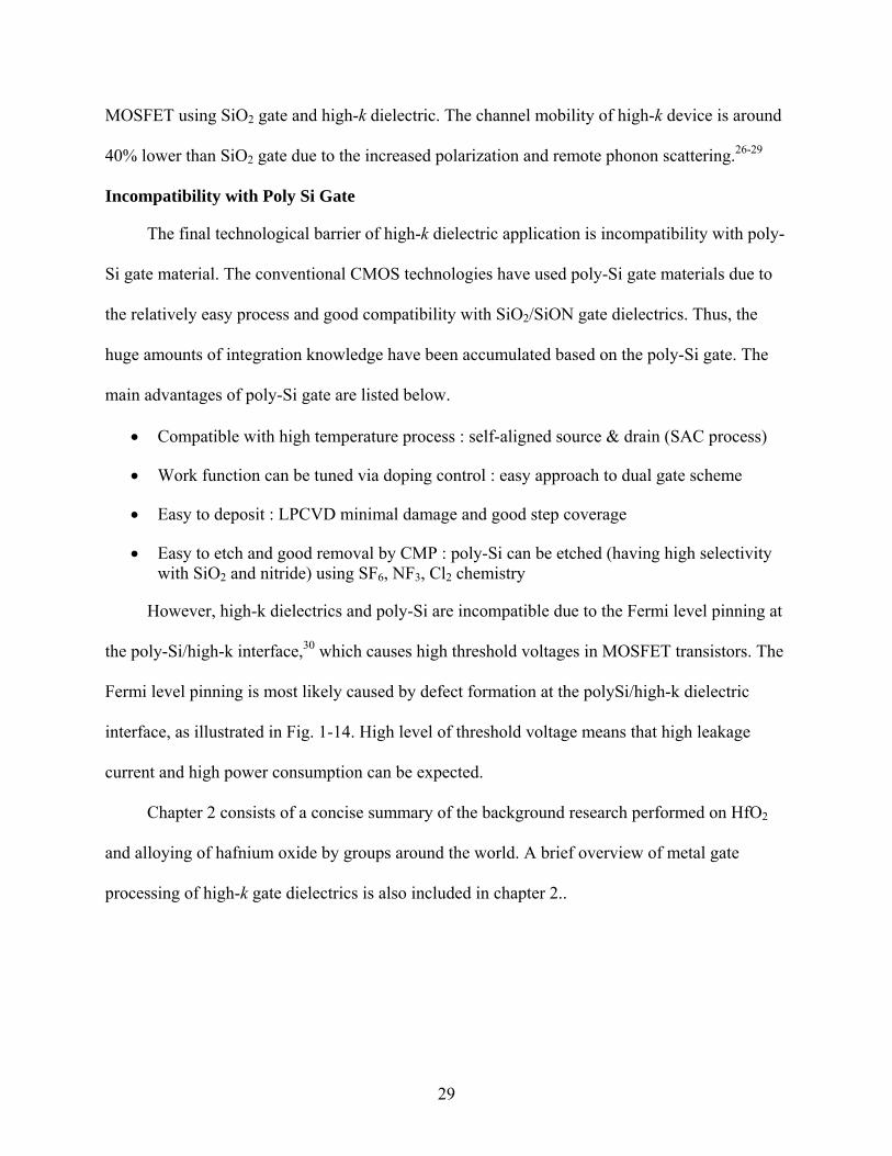
However, high-k dielectrics and poly-Si are incompatible due to the Fermi level pinning at
the poly-Si/high-k interface,30 which causes high threshold voltages in MOSFET transistors. The
Fermi level pinning is most likely caused by defect formation at the polySi/high-k dielectric
interface, as illustrated in Fig. 1-14. High level of threshold voltage means that high leakage
current and high power consumption can be expected.
Chapter 2 consists of a concise summary of the background research performed on HfO2
and alloying of hafnium oxide by groups around the world. A brief overview of metal gate
processing of high-k gate dielectrics is also included in chapter 2..
29
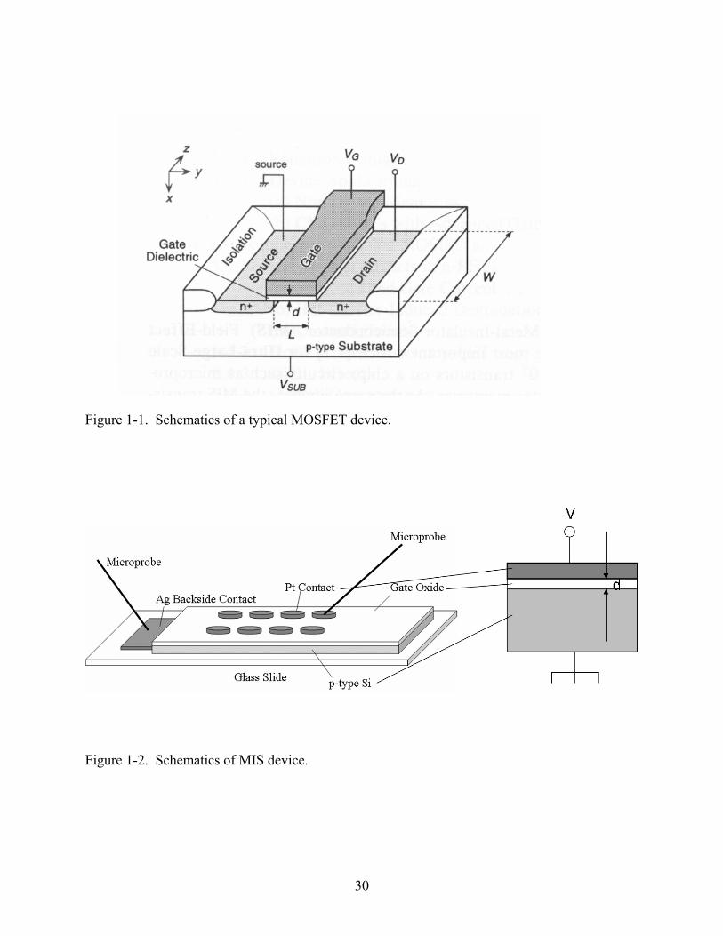
Figure 1-1. Schematics of a typical MOSFET device.
Figure 1-2. Schematics of MIS device.
30
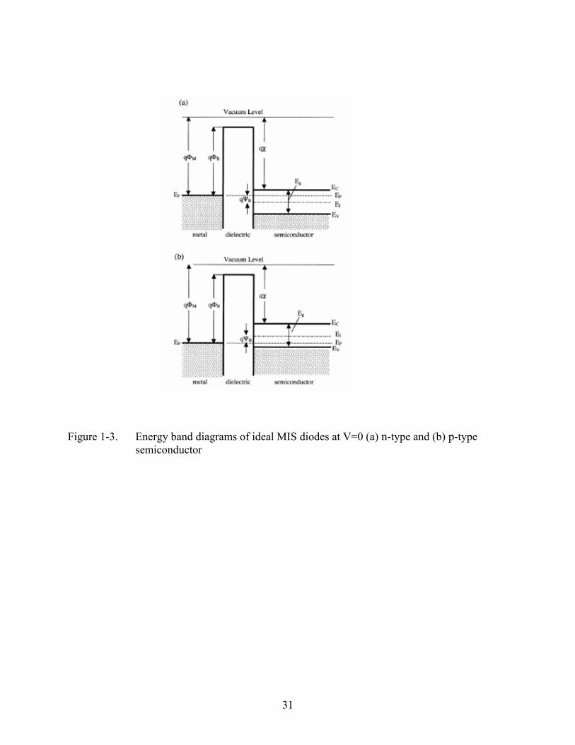
Figure 1-3. Energy band diagrams of ideal MIS diodes at V=0 (a) n-type and (b) p-type semiconductor
31
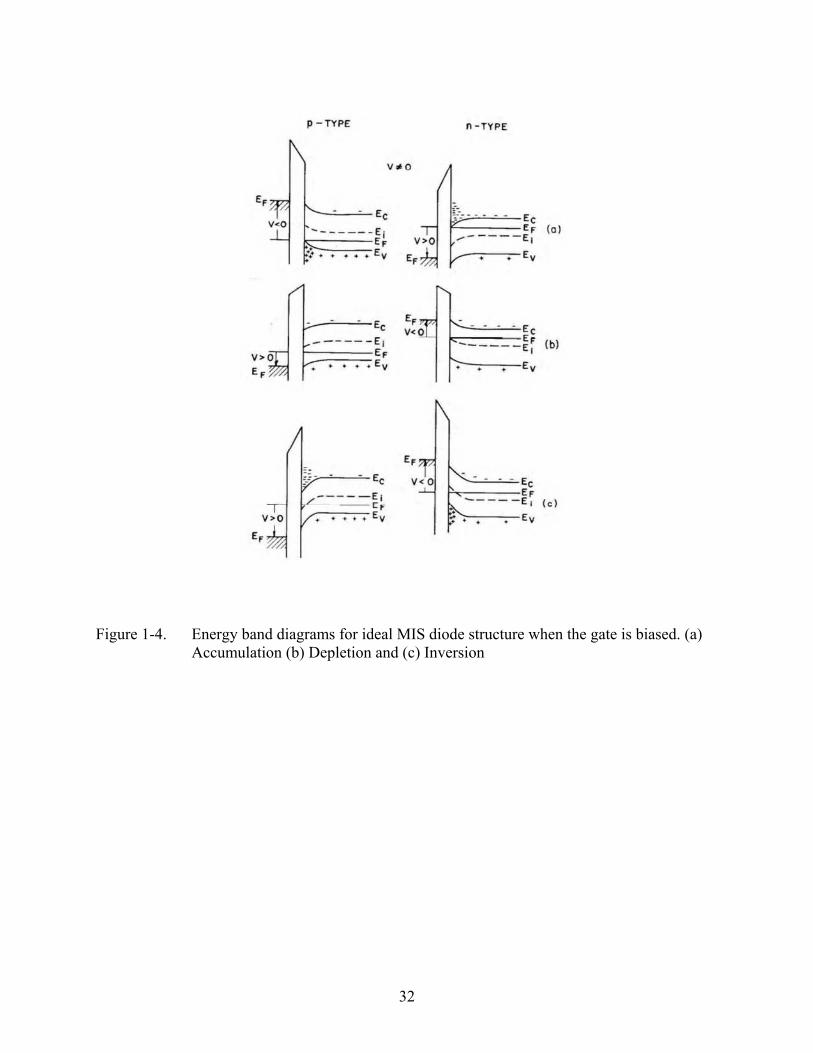
Figure 1-4. Energy band diagrams for ideal MIS diode structure when the gate is biased. (a) Accumulation (b) Depletion and (c) Inversion
32
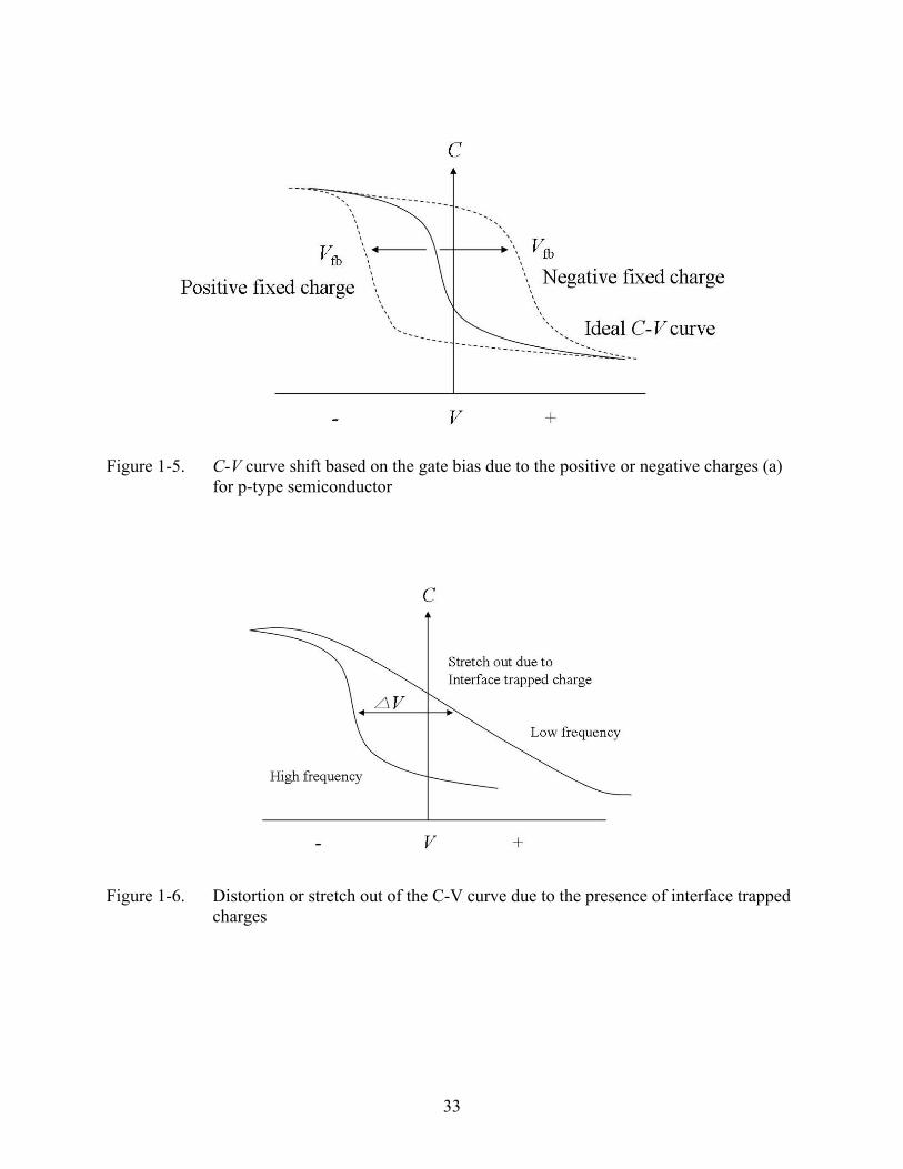
Figure 1-5. C-V curve shift based on the gate bias due to the positive or negative charges (a) for p-type semiconductor
Figure 1-6. Distortion or stretch out of the C-V curve due to the presence of interface trapped charges
33
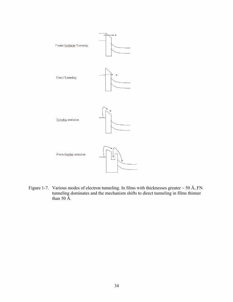
Figure 1-7. Various modes of electron tunneling. In films with thicknesses greater ~ 50 Å, FN tunneling dominates and the mechanism shifts to direct tunneling in films thinner than 50 Å.
34
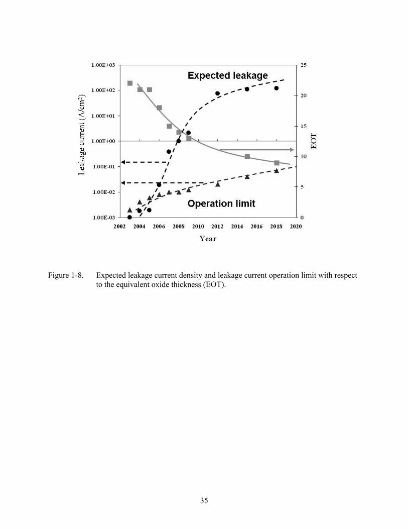
Figure 1-8. Expected leakage current density and leakage current operation limit with respect to the equivalent oxide thickness (EOT).
35
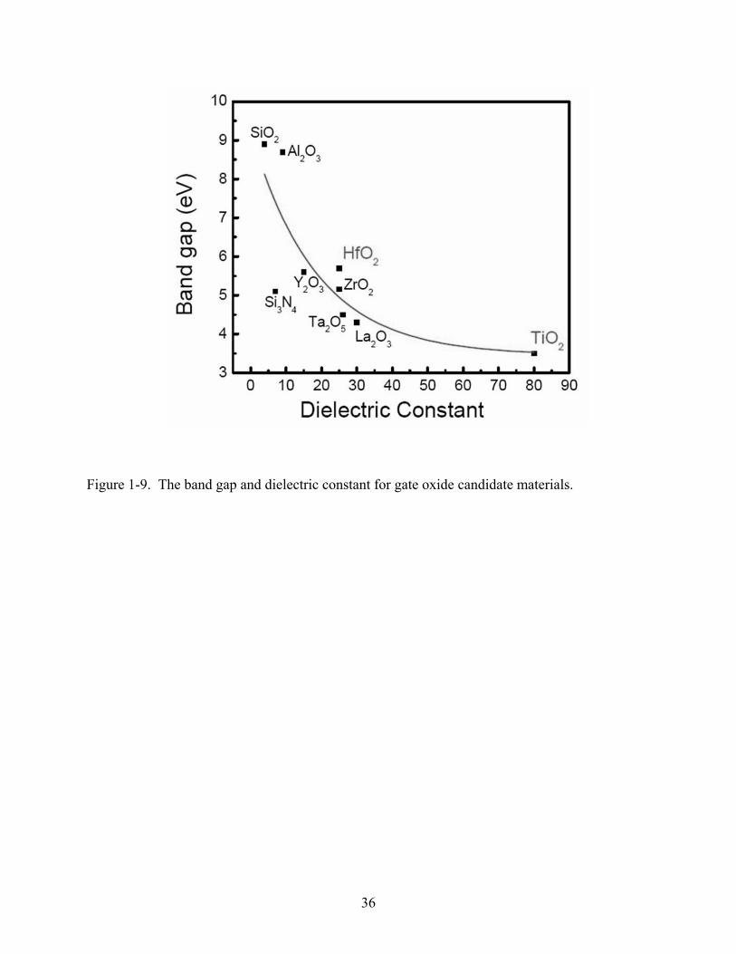
Figure 1-9. The band gap and dielectric constant for gate oxide candidate materials.
36
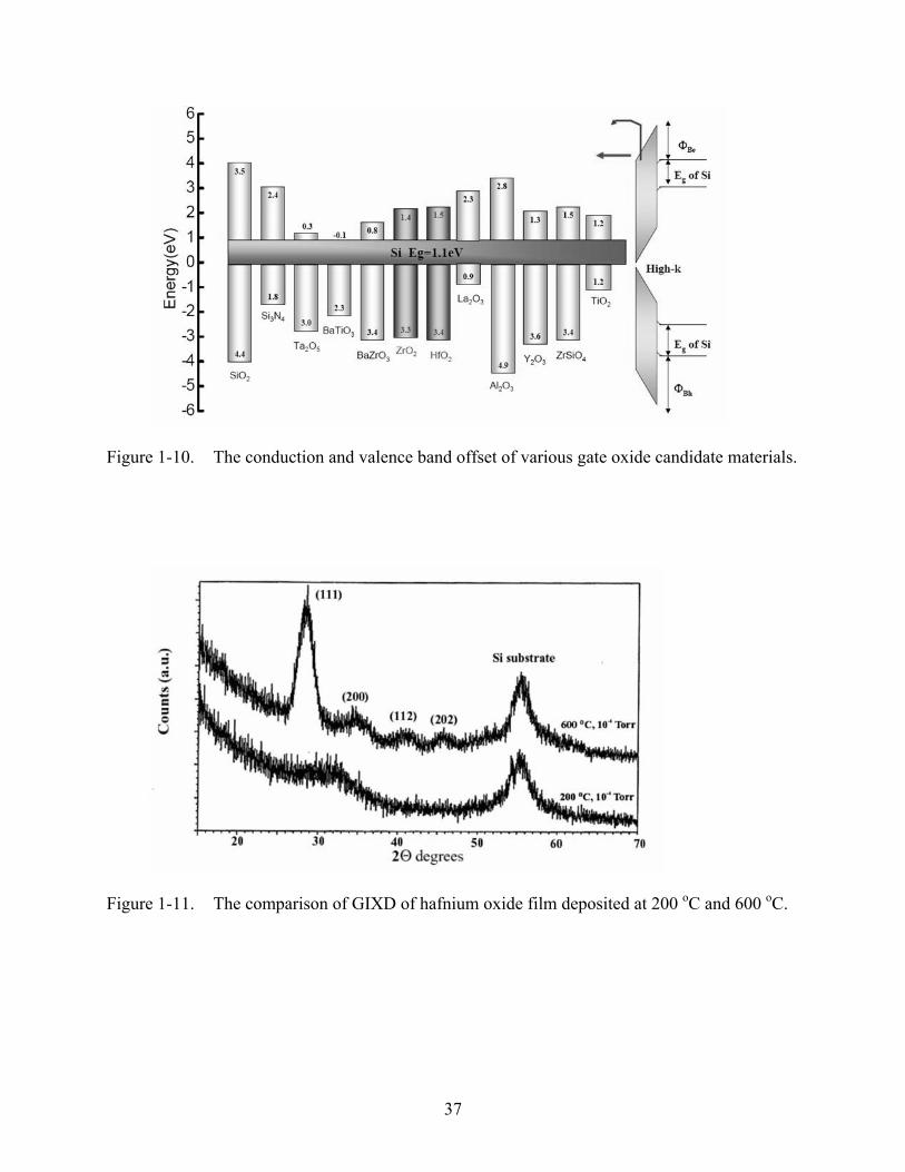
Figure 1-10. The conduction and valence band offset of various gate oxide candidate materials.
Figure 1-11. The comparison of GIXD of hafnium oxide film deposited at 200 oC and 600 oC.
37
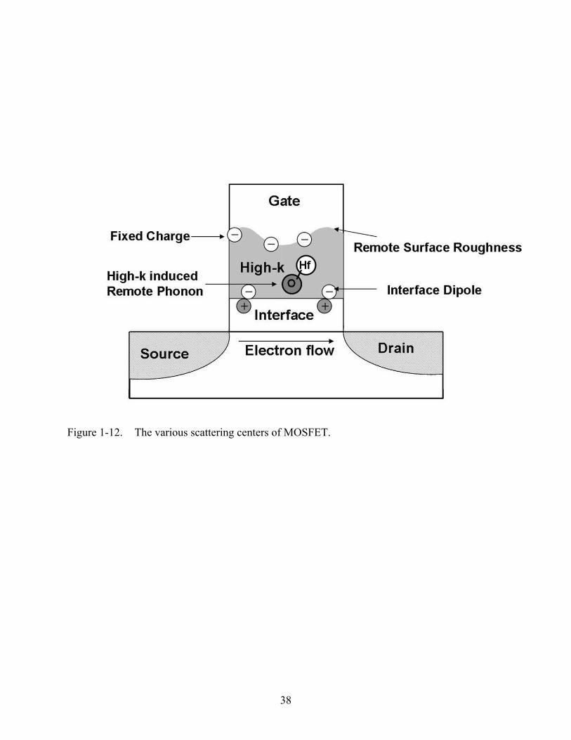
Figure 1-12. The various scattering centers of MOSFET.
38
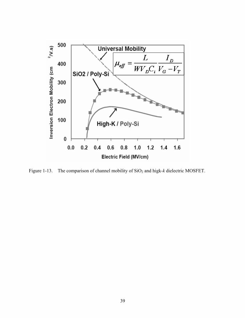
Figure 1-13. The comparison of channel mobility of SiO2 and higk-k dielectric MOSFET.
39
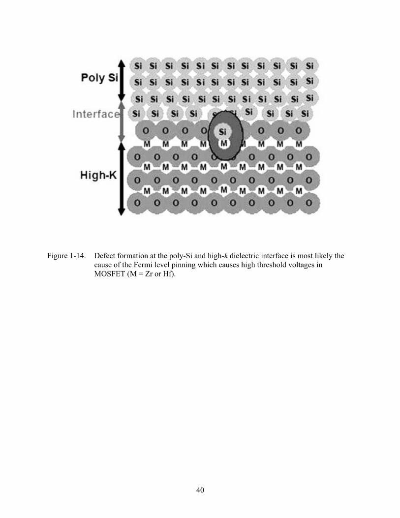
Figure 1-14. Defect formation at the poly-Si and high-k dielectric interface is most likely the cause of the Fermi level pinning which causes high threshold voltages in MOSFET (M = Zr or Hf).
40
CHAPTER 2 LITERATURE REVIEW
HfO2 and Hf-Silicate Dielectric
A significant amount of research and monetary funding has gone into finding alternate
gate dielectric materials to replace the current gate oxide (SiO2) in the past decade. Several
variations in conventional thin film processing have been developed to tailor the material and
electrical properties of the gate dielectric to attain the desired objectives. The material systems
investigated as prospective candidates include Al2O3, HfO2, ZrO2, Ta2O5 and alloyed oxides of
Hf, Ti and Al. Processes such as nitridation of the dielectric films, surface nitridation of Si prior
to dielectric growth, plasma treatments, ultra-violet (UV) radiation assisted thin film processing
and UV assisted metal oxidation are among the few of the variations in conventional thin film
processing. Though there is a huge disparity in the obtained results on a particular material
system, several new constraints are now in place for selection of the next generation gate
dielectric. Factors such as minimal threshold voltage instability, microstructure stability at high
temperatures (~ 1000 oC), minimal charge trapping and carrier mobility closer to SiO2 (> 90%)
have become the key norms nowadays.
Bonding and Electrical Properties
Among all the above-mentioned material systems, HfO2 and Hf silicate like structures have
shown the most promise as future gate dielectrics. The key advantages of hafnium oxide include
a relatively high dielectric constant (~ 21-25) depending on processing conditions, reasonable
band offsets for acceptable leakage properties and thermodynamic stability with Si.4,31 Hf silicate
exhibits an interface, which is the closest to Si-SiO2 interface due to similar bonding chemistry
and coordination. Hf silicates also have a larger bandgap (~ 6 eV) with favorable conduction
band alignments with Si and have also been reported to be thermally stable with Si at high
41
temperatures. Hf silicates exhibit dielectric constants ranging from 8 – 14 depending on the
amount of Hf present in the films.4,11,12 Bluementhal et al. have reported that the structure of
ZrSiO is tetragonal and is composed of parallel chains of atoms consisting of – Zr - 2O – Si - 2O
– Zr – 2O – Zr and so on where each Zr and Si atom shares bonds with four oxygen atoms within
the chains.32 In addition, each Zr and Si atom also shares two oxygen atoms with the
neighbouring chains providing a three dimensional stability to the material. The structural units
are ZrO2 and SiO2. A dielectric constant of 12.6 was reported for ZrSiO4 by Bluementhal et al.
which is reasonable considering that this material system is comprised of SiO2 (ε ~ 3.9) and ZrO2
(ε ~ 25). Analogously, HfSiO4 is also expected to have a similar structure due to its chemical
similarity with ZrO2. The HfSiO4 is also expected to exhibit a dielectric constant of ~ 12-15
based on the processing conditions, microstructure of the film and on the relative Hf content.
Considering all the above-mentioned properties of Hf and Zr silicates, they are promising
candidates for alternate gate dielectric applications.
HfO2 Gate Dielectrics
L. Kang et al. have investigated the electrical and material properties of R.F. sputtered
HfO2 films on Si.33 The films (~ 45 Å thick) were deposited at room temperature in a controlled
O2 ambient to suppress excessive growth of the low k interfacial layer at the dielectric-Si
interface. They reported an equivalent oxide thickness (EOT) of ~ 13.5 Å. Pt was used as the
gate electrode. The estimated leakage current densities were ~ 10-4 A/cm2. For comparison, a 13
Å SiO2 film is expected to exhibit a leakage current density of 100 A/cm2 or higher. In addition
to an EOT of 13.5 Å, hysteresis values lower than 100 mV were also obtained. This study shows
that the HfO2 can be implemented as the next generation gate dielectric when processed under
the right processing conditions. The effects of high temperature treatment of HfO2 dielectrics
were studied by S. W. Nam et al.34 The films were deposited by DC magnetron sputtering
42
process at room temperature. First, a layer of Hf metal was deposited as an oxidation barrier and
then a thin layer of HfO2 was deposited on the Hf metal in an ambient of Ar and O2. The Hf
metal layer helps to form HfO2 by reducing the native oxide on Si. The as-deposited films were
found to be amorphous. However, the monoclinic and orthorhombic phases of polycrystalline
HfO2 were reported to emerge after annealing at 650 oC and 900 oC respectively in O2 and N2
ambient. The measured EOT values were ~ 19 Å for N2 annealed samples and ~ 28 Å for O2
annealed samples. The increase in EOT is believed to be due to the oxidation of the underlying
Si substrate. Lee et al. reported EOT values around 9 Å with reasonably low leakage in HfO2
MOS capacitors with Pt gate electrodes.35 They also reported a slight growth of an interfacial
layer at the HfO2 – Si interface. However, the main concerns of implementing a metal gate are
lack of thermal stability and unfavorable band alignments. Pt is considered to be inadequate for
NMOS applications due to its large work function (~ 5.3 eV). Nevertheless, Pt, due to its
chemical inertness, is still an effective gate electrode for preliminary studies of gate dielectrics
through MOS capacitors.
The main issues with HfO2 are the growth of the low k interfacial layer at the hafnia-Si
interface and the amorphous to polycrystalline transformation at high temperatures. The
interfacial layer severely reduces the overall dielectric constant of HfO2 and the formation of
grain boundaries is deleterious for a reliable device operation as they act as leakage paths. Hence,
from an EOT point of view, HfO2 is reaching its scalability limits due to the above-mentioned
issues. Other methods such as alloying HfO2 with high permittivity materials such as TiO2 are
being actively considered to obtain EOT values of 15 Å and lower with acceptable leakage
current densities.36
43
Hf-Silicate Dielectrics
Hafnium silicate based chemistries were also / are still being heavily investigated for their
attractive properties such as a moderate k, large bandgap (~ 6 eV) and excellent interfacial
stability with Si. Wilk et al. have reported on the electrical and material properties of Hf-Si-O
material system.37 The films were sputter deposited at various substrate temperatures ranging
from 25 – 600 oC. No evidence of Hf-Si formation was detected by XPS analysis and MOS
capacitors were fabricated on the Hf-Si-O dielectric films using Au as the gate electrode for its
relatively large work function (~ 5.3 eV). The work function of the Au electrode is helpful in
creating a zero flatband voltage condition. The films deposited at 500 oC on Si exhibited a ε
value of 11 and an EOT of 17.8 Å. No quantum mechanical corrections were included in the
extraction of EOT values. The films exhibited leakage current densities around 10-6 to 10-5
A/cm2 at 1 to 1.5 V bias range. In addition to excellent preliminary electrical results, the Hf-Si-O
films were also found to be thermally stable after an 800 oC anneal in N2 ambient. The Hf-Si-O
and Si interface was found to be atomistically sharp after the high temperature annealing. De
Gendt et al. have reported on Hf silicates processed by atomic vapor deposition (AVD) at 550
oC.38 The films exhibited dielectric constants ranging form 6 – 14 depending on the film
composition. EOT values of 13 Å were extracted with leakage current densities lower than 10-2
A/cm2. The flat band voltage was found to vary with the film composition from -0.1 V to 0.45 V.
These studies establish the promising aspects of Hf-Si-O material systems as alternate gate
dielectrics. However, a sub 13 Å with leakage current densities of 10-4 A/cm2 and lower are more
desirable for high performance applications and for reliable device operation. A composition
window for Hf content is extremely important to tailor the electrical properties to suit the
objectives.
44
Nitrogen Incorporation in Hafnia Film
Nitrogen is a well-known diffusion barrier to oxygen and is regularly used in CMOS
processing. Si3N4 is an extension of the current gate dielectric. It has a dielectric constant of ~ 8
depending on the processing conditions. Given the diffusion barrier properties and the fact that
the nitrides tend to have a better electrical response in comparison to oxides, extensive research
has been done on incorporating nitrogen in HfO2.
Kang et al. have reported on the electrical and interfacial properties of hafnium oxynitride
gate dielectrics processed by reactive sputtering.39 The films were postannealed in N2 ambient at
650 oC and the nitrogen incorporation was confirmed by XPS analysis of Hf 4f and Si 2p peak
regions. In comparison to the control HfO2 films, Hf-ON films exhibited lower EOT values and
leakage current densities. Even after a post metal anneal at 950 oC in N2, an EOT of 9.6 Å was
obtained indicating excellent thermal stability. This enhanced electrical response was attributed
to the presence of Si-N bonds at the film-Si interface and due to the blocking of oxygen by
nitrogen bonding.
Kirsch et al. investigated the interfacial properties of nitrogen doped HfO2 films and have
reported on the impact of nitrogen on the electrical properties.40 A Hf target was used to initially
sputter Hf onto HF terminated Si and NH3 annealed Si substrates. The nitridation of Si was
achieved by pre-annealing the Si substrates in an NH3 ambient for 30 seconds at 700 oC. The as-
deposited Hf films were later annealed in N2 ambient for 10 seconds at 600 oC. Given the affinity
of Hf atoms towards oxygen, oxidation was merely accomplished by exposing the Hf films to the
oxygen present in the processing ambient. The HfO2 films on nitrided Si exhibited lower leakage
current densities (~ 10-5A/cm2 at - 1 V) in comparison to the control HfO2 sample. A dielectric
constant of 19 was obtained from the nitrided sample in comparison to a dielectric constant of 17
from the un-nitrided sample.
45
Recently, there have been several reports41-44 on the incorporation of both Si and N into
HfO2 (i.e. HfSiON, hafnium silicon oxynitride) which was found to improve thermal stability
further compared to HfON. Especially, M.R. Visokay et al. performed comparative study on the
effects of nitrogen incorporation for hafnium oxide and hafnium silicate films. According to M.R.
Visokay’s report 30,43, incorporation of both Si and N into HfO2 is inevitable to increase
crystallization temperature and avoid phase separation at CMOS processing temperature.
However, dielectric constants are reduced in HfSiON due to the presence of silicon oxide bonds
with much lower dielectric constant than HfO2. According to a report,44 HfSiON with optimized
composition remained amorphous state up to 1100 oC whereas dielectric constant decreased
down to ~10. In terms of application, the HfSiON appears to be very promising materials for the
low power devices rather than high speed device requiring further scaling-down of EOTs < 10Å
in the near future.
From the above studies, it is clearly evident that nitrogen incorporation can play an
important in enhancing the electrical properties of the HfO2 stack. However, the main drawback
with nitrogen incorporation is the increase in Dit values. Fedorenko et al. have performed studies
on the impact of nitrogen addition on the density of interface traps. They have reported an
increase in the interface trap density in the upper part of the Si band gap and have concluded that
in this energy range, nitrogen prevents the passivation of interface traps by forming gas
annealing or by hydrogen.45
Ultra-violet (UV) Assisted Thin film Processing
Ultra-violet radiation assisted thin film processing and thin film oxidation is an interesting
alternative to achieve an enhanced degree of oxidation in Si.46,47 At temperatures as high as 850
oC, the oxidation rate during the thermal oxidation process of Si is around 2Å/minute despite a
surplus oxygen supply. This low rate of oxidation is mainly attributed to a large energy barrier or
46
activation energy (> 1.5 eV) required for oxygen to diffuse through the oxide to reach the
underlying Si. When an UV source is employed in thin film processing, the energy of the
photons with wavelengths around 183 nm and lower is sufficient enough to convert the
molecular oxygen, which is regularly used for oxidation purposes, into atomic oxygen and ozone
(O3). This newly generated ozone further dissociates into O2 and atomic oxygen O (1D) ranging
from several percent to greater than 10%. The above-mentioned steps can be represented by the
following equations.48
O2 + hν 2O (2-1) →
O + O2 +M O3 + M (2-2) →
O3 + O 2O2 (2-3) →
O3 + O2 O2 + O2 + O (2-4) →
Further interaction of ozone with the short wavelength (254 nm and lower) photons will
lead to the dissociation of ozone as shown by the equation 2-5.
O3 + hν O2 + O (2-5) →
Photo-induced transitions occur from the conduction band of Si to the conduction band of
SiO2 (3.15 eV) and from the valence band of Si to the valence band of SiO2 (4.25 eV) when the
sample is irradiated. Hence, with the influence of UV illumination, the Si is supplied with atomic
oxygen from the gas interface and electrons from Si/SiO2 thus the probability of ionization of
oxygen species is enhanced. Boyd et al. claim that the atomic oxygen is more reactive than
molecular oxygen and has the ability to move more easily through the SiO2 matrix enabling
enhanced oxidation rates. This effect has also been reported to be more pronounced at lower and
moderate temperatures (~ 450 oC). Ramanathan et al. have investigated ultraviolet radiation
assisted oxidation of high -k dielectric films.49-51 Metal oxides (Zr and Hf) were sputter deposited
47
at room temperature on thin layers of SiO2 or nitrided SiO2. The films were oxidized for various
times (0.5 – 60 minutes) and at various oxygen partial pressures (80 mTorr – 600 Torr). The
oxide films were found to be polycrystalline with no preferred orientation. Normally, the
oxidation of a metal occurs by (i) physisorption and (ii) dissociative chemisorption. The oxygen
molecules initially form weak Van der walls forces with the metal. Subsequently the oxygen
molecules dissociate into atomic oxygen and form metal-oxide bonds. This dissociation of
molecular oxygen requires an activation energy and is the rate limiting step. With the addition of
an UV radiation source, the chemisorption step proceeds without any barrier as the energy of the
183 nm wavelength radiation is high enough to create atomic oxygen. The initial oxidation is rate
is increased when compared to natural oxidation. Moreover, the films after UV oxidation were
found to be completely oxygenated (free of oxygen deficiencies) and exhibited superior electrical
performance. Hence the benefits of UV oxidation are two fold (i) enhanced oxidation rate an (ii)
enables the formation of a stoichiometric oxide. Zirconia films up to 5 nm in thickness were
grown by the UV oxidation at room temperature whereas the natural oxidation was found to self-
limiting at 1.5 nm.
Punchaipetch et al. reported on room temperature ultraviolet (UV) oxidation of hafnium
silicide films for high-k gate dielectric applications.52 The Hf silicide films were deposited on
hydrogen terminated Si substrates at room temperature by magnetron sputtering using Ar as the
carrier gas. The Hf silicide films were subsequently oxidized under UV/O3 exposure for
conversion of Hf silicide into Hf silicate. Angle resolved x-ray photoelectron spectroscopy (AR-
XPS) analysis confirmed the oxidation of Hf silicide films into Hf silicate. The films with ~ 12%
Hf exhibited a dielectric constant of 8-9 and a leakage current density of ~ 4 × 10⁻⁵ A/cm2 at a
bias of Vfb + 1 (volts). A 4.7 nm thick Hf silicate film had minimal interfacial layer formation
48
and an equivalent oxide thickness of 26 Å (without quantum mechanical corrections) was
measured by C-V measurements at 100 KHz. The above-mentioned studies on UV assisted
processing of gate dielectric films establish the efficacy of UV illumination towards achieving
enhanced rates of oxidation and eliminating oxygen deficiencies in the films. With the current
drive towards low temperature device processing, UV assisted oxidation technique is an
interesting alternative to fabricate stoichiometric metal oxide or metal silicate films for alternate
gate dielectric applications.
Metal Gate Process for CMOS Device
To meet the scaling trends and overcome degraded inversion capacitance due to poly-
depletion, metal gate electrodes are being evaluated as a replacement to poly-silicon electrodes.53
Metal gate electrodes have the added benefit of reducing the gate resistance and eliminating the
threat of boron penetration from p+ poly-silicon into the channel region. For bulk CMOS devices,
simulations indicate that the desired work function for NMOS (PMOS) electrodes is near the
conduction (valence) band edge of silicon.54,55
Candidate Metals for Metal Gate Application
A quick review of the work functions of the elements3 shows a periodicity between work
function and atomic number. Work functions increase from left to right across a row on the
periodic table (Figure 2-1). This indicates that metals with work functions above the conduction
band edge of Si (<4.1 eV) are typically in the first three columns of the periodic table.
Alternatively, metals with work functions below the valence band edge of Si (>5.2 eV) tend to be
late transition metals. In particular, the platinum group metals such as Pt, Ir, Os, Au, Ni, Ru, Pd,
and Rh have high work functions. The vast majority of the transition metals have work functions
that exist within the band edges of silicon (4.1 eV < Φms < 5.2 eV). The work functions of metals
49
have been studied using a variety of techniques. These include the photoelectric effect,
thermionic emission, field emission, contact potential difference, and extracted from MOS
capacitors. These techniques do not necessarily produce the same value which complicates the
search for candidate materials.
To further narrow the list of viable metal gate electrodes, candidates must also possess
thermal stability up to the dopant activation temperatures of approximately 900-1000 °C.
Thermal stability includes the absence of gross reactions between the dielectric and other
surrounding materials, no inter-diffusions with surrounding materials, sufficient bulk phase
stability, and smooth interfaces with the dielectric. Due to these stringent thermal requirements
refractory metals such as W, Re, Ta, and Mo have attracted interest.
Metal nitrides and carbides have also gathered attention as metal gate electrodes. These
materials are renowned for their use as diffusion barriers in the semiconductor industry.
Transition metal nitrides and carbides are comprised of a face-centered-cubic metal structure
with nitrogen or carbon atoms occupying the octahedral interstices. This results in the rock-salt
structure (NaCl). Since N and C occupy interstices the lattice parameter is typically only ~5%
larger than that of the pure metal compound. Stuffing the interstices with N or C helps give these
materials their excellent diffusion barrier properties. These materials exhibit metal-like
conduction, but at the same time are highly refractory compared to the pure metal constituent. It
is believed that a mixture of metallic, covalent, and ionic bonding character is responsible for
this behavior.56
There have been numerous studies on the work function of interstitial nitrides for
electrode and emitter applications. This includes MoN,57
WN,58
NbN,59
TaN,58,60
TiN,57,59-61
ZrN,59
and HfN63
among others. TiAlN has also been widely studied as a metal gate electrode. 64
Although it is a ternary metal nitride, it is more closely related to the binary nitrides than the
50
amorphous ternary metals because this compound exists in the rock salt structure for Al:Ti ratios
<0.40 and in a mixture of rock salt and wurtzite structures for >0.40 Al:Ti ratio.64
TiAlN loses its
conductive properties with increasing presence of the AlN wutzite phase.
Ternary alloys of a transition metal (TM), silicon, and nitrogen have also been widely
investigated for their properties as diffusion barriers. These films are found to exist in a highly
metastable amorphous structure.65
This property makes them excellent diffusion barriers to
elevated temperatures. Ta-Si-N is currently being investigated as a stable NMOS electrode
candidate.
Another problem is the need to integrate two metals with different work functions to build
both NMOS and PMOS devices. This is easily done with poly-silicon electrodes by ion
implanting n-type or p-type dopants into NMOS or PMOS electrodes, respectively. The
implantation is performed selectively by patterning the NMOS region with photoresist while
implanting dopants into the PMOS regions and vice-versa. The implants shift the Fermi energy
of n-type poly-silicon towards the conduction band and shift the Fermi energy of p-type poly-
silicon towards the valence band to achieve the appropriate work functions and low device
threshold voltage.
Different integration approaches have been proposed for metal gates. Both conventional
integrations and replacement gate67
integrations have been proposed. Replacement gate
integrations dramatically reduce the temperatures that the metal gate must withstand because the
source/drain activation anneals are performed before the metal gate is deposited. The other
integration approaches can be classified into one of four types. These include stacked dual metal
gate integration, metal alloy integration, nitrogen modulation integration, and fully-silicided
metal gate (FUSI) integration.
51
The integration approach that most easily accommodates vastly different metals for NMOS
and PMOS electrodes is the stacked dual metal gate integration (Figure 2-2). This integration
involves depositing one metal over both the NMOS and the PMOS regions. Then patterning one
of the two regions and removing the electrode using a wet etch chemistry that is selective to the
underlying gate dielectric. A second metal can then deposited over the first metal. The most
difficult aspect of this integration is the plasma etching two different gate stacks of different
heights. This integration has been demonstrated on Si3N4 gate dielectric and on HfO2 gate
dielectrics.68
In the metal alloy approach two metals are initially deposited on top of each other. Either
the NMOS or PMOS region is then patterned so that the top metal can be selectively removed. A
high temperature annealing process is then used to inter-diffuse the two metals. This leaves an
inter-diffused metal for one of the electrodes and an elemental metal for the other electrode
(Figure 2-3). This approach has been performed using Ru-Ta69,70
, Ti-Ni71
, and Pt-Ta72
alloys. The
alloyed electrode approach has two foreseeable problems. First, it may be difficult to get one
alloy system to span the entire 1.1 eV range to meet the NMOS and PMOS work function
requirements. Second, some of the elements used in the alloy may not be thermally stable in
contact with a high permittivity dielectric. The nitrogen modulation integration has been reported
in two forms (Figure. 2-4). The first method is to ion implant nitrogen into a metal to shift its
work function. This has been demonstrated for Mo-based electrodes,73
and for TiN-based
electrodes where the N concentration is modulated via implantation of N.74
Adjusting the
nitrogen concentration has also been accomplished by solid-state diffusion of nitrogen from a
nitrogen-rich film into a nitrogen-deficient film. Like the alloy approach, it may be difficult to
52
span the entire work function range to meet the NMOS and PMOS electrode requirements by
implanting nitrogen.
Fermi Energy Level Pinning
A roadblock to successful implementation of metal gate electrodes with the proper work
functions is Fermi level pinning. Fermi pinning is a consequence of forming an interface
between a metal and a dielectric (or semiconductor). When an interface is formed, the effective
metal work function becomes “pinned” at a different energy than its vacuum work function. This
results from interfacial charge exchange between the metal Fermi level and gap states at the
metal-dielectric interface causing it to shift with respect to its unpinned location. A recent
comprehensive review of Schottky barrier concepts has been published.75
Fermi level pinning of poly-Si76
and metal electrodes77
on HfO2 has been investigated, and
Fermi pinning models have been extensively tested on a broad class of interfaces.78.79
The most
widely accepted of these models is the metal induced gap states (MIGS) model. The origin of the
gap states in the MIGS model is from the dangling bonds of under-coordinated surface atoms.
These dangling bonds produce surface states that are dispersed in continuum at energies
throughout the band gap of the dielectric. In the MIGS model, when a metal is placed in contact
with a dielectric, the metal surface states induce the gap states in the dielectric. This results in
interfacial charge exchange between the metal and the dielectric gap states causing the metal
Fermi level to shift with respect to its unpinned location towards a characteristic energy level in
the semiconductor
Other models have been proposed where the states responsible for Fermi level pinning
have an extrinsic origin. These include the unified defect theory where a specific defect, with a
high density of states at a given energy is responsible for the pinning behavior; disorder-induced
53
gap states, where variations in bond length and bond angle at an interface result in states
dispersed across the band gap; and finally the effective work function theory where the effective
work function is determined by the work function of a metallic species that precipitates at the
interface.
Strain Engineering for High Channel Mobility MOSFET
Aggressive scaling of complementary metal-oxide-semiconductor (CMOS) technology
requires a high drive current to increase circuit speed. Both the gate capacitance and carrier
mobility can improve the drive current. The high-k dielectrics and metal gate can increase gate
capacitance. However, mobility degradation, and interfacial layer scalability delay the
introduction of high-k dielectrics into industrial applications. In order to enhance the mobility,
mobility enhancement by strain, new materials such as Ge or SiGe channels, and new substrate
orientation such as (110) and (111) offers alternative ways to increase drive current.80 Applying
stress to induce appropriate strain in the channel region of metal-oxide-semiconductor field
effect transistors (MOSFETs) increases both electron and hole mobilities in the strained
channel.81,82 The mobility enhancement mechanism is explained by band modification. The
easiest way to check the strain on the Si channel is stress inducement by bending the Si wafer
directly (mechanical strain). The mechanical strain is called ‘Package-strain’ due to strain
inducement at package process. Package strain can improve the NMOS and PMOS device
performance after the fabrication of VLSI and the cost is relatively low.
Band Modification Model
The enhanced electron mobility can be explained by the conduction band modification
induced by the biaxial tensile strain, which lifts the six-fold degeneracy in the conduction band
and lowers the energy of the two valleys along the growth direction (001) (Figure 2-5). The
electrons occupy preferentially the two lower energy valleys, which has the low effective in-
54
plane transport mass. Energy splitting also suppresses intervalley scattering. The mobility at the
low field (<∼0.4 MV/cm) is dominated by impurity scattering (Coulomb scattering), the high
field mobility (>1MV/cm) is determined by the roughness scattering, and the intermediate field
mobility is dominated by the phonon scattering. Note that the effective electrical field is
perpendicular to the channel and is controlled by the gate voltage and device structure.
Conventionally, the roughness scattering is originated from the oxide/Si interface. Electron
mobility enhancement of substrate-strained Si devices at high channel doping (up to 6 ×
1018/cm3 ) is reported. If the inversion layer carrier concentration is low, the strain-induced
mobility enhancement decreases due to the ionized impurity scattering, but the enhancement
recovers at higher inversion charge concentrations, where the screening is more efficient.
Application Scheme for Future Device
Substrate-strain results in biaxial strain to channel and enhances electron and hole
mobilities. However, cost, scalability, and complexities such as low-defect Si1−xGex buffers, low
thermal budget, and integration, remain issues for production. Moreover, the hole mobility of the
Si channel at high fields is not improved significantly except at the Ge or dual channel because
the energy separation between light and heavy hole bands is not enough due to the quantization
effect. In contrast, uniaxial strain offers similar electron mobility enhancement compared with
biaxial strain, while the hole mobility improvement is more significant at high field.83 For <110>
channel orientation on (100) substrates, the uniaxial compressive strain parallel to the channel
and the uniaxial tensile stress transverse to the channel result in larger hole mobility
enhancement than biaxial tensile strain at the same stress level. Hole mobility enhancement with
these uniaxial stresses is mainly due to band warping, resulting in the decrease of the transport
effective mass along the <110> direction.84 Furthermore, these uniaxial strains may have lower
55
surface roughness scattering due to the large out-of-plane effective mass (less wave function
penetration into dielectrics).83 Process induced strain has been used to produce the desired
uniaxial strain.85 Several approaches (Figure 2-6) such as silicon nitride (Si3N4 ) cap layer,
shallow-trench isolation (STI), silicidation processes, and embedded SiGe S/D have been utilized
to realize the local strain.86
Silicon nitride film is well-known to produce a high level of stress [Figure 2-6(a)]. Si3N4
film can have either tensile or compressive strain depending on the deposition conditions, and
the drive currents of both n- and p-channel MOSFETs can be improved by controlling the stress
of the Si3N4 layer selectively. The tensile cap layer deposited by thermal chemical vapor
deposition (CVD) can improve the performance of NMOS due to the induced tensile strain in the
channel region, while the compressive cap layer deposited by plasma enhanced CVD can
improve the PMOS due to the induced compressive strain in the channel region.86 Shimizu et al.
reported that a highly tensile strained Si3N4 cap layer can improve NMOS performance but
degrade PMOS performance.86 Capping a highly-tensile Si3N4 layer shows 25% NMOS drain
current improvement,87 while selective Ge implanted into the capping layer can recover the
degradation of PMOS devices.
The strained PMOS transistor features an epitaxially grown strained SiGe film embedded
in the S/D regions using a selective epitaxial growth was reported by Intel [Figure 2-6 (b)].88 The
source and drain regions, made of an alloy of Si1−xGex, are deposited in the recessed source and
drain region. The lattice constant of the SiGe alloy is larger as compared to the bulk Si due to the
inclusion of Ge. The larger lattice constant of Si1−xGex creates a compressive stress in the channel
of a 45-nm gate length transistor between the source and drain regions, thereby resulting in
significant hole mobility improvement (>50%) with 17% Ge incorporation. It is interesting to
56
note that hole mobility is also enhanced at the high field region for the uniaxial compressive
strain parallel to the channel. By integrating and taking advantage of aforementioned strain
engineering techniques, CMOS performance can be further improved. As a final note for process
induced strain, the process strain is effective for the 90-nm node and beyond, but its
enhancement effect diminishes for large channel devices.
57
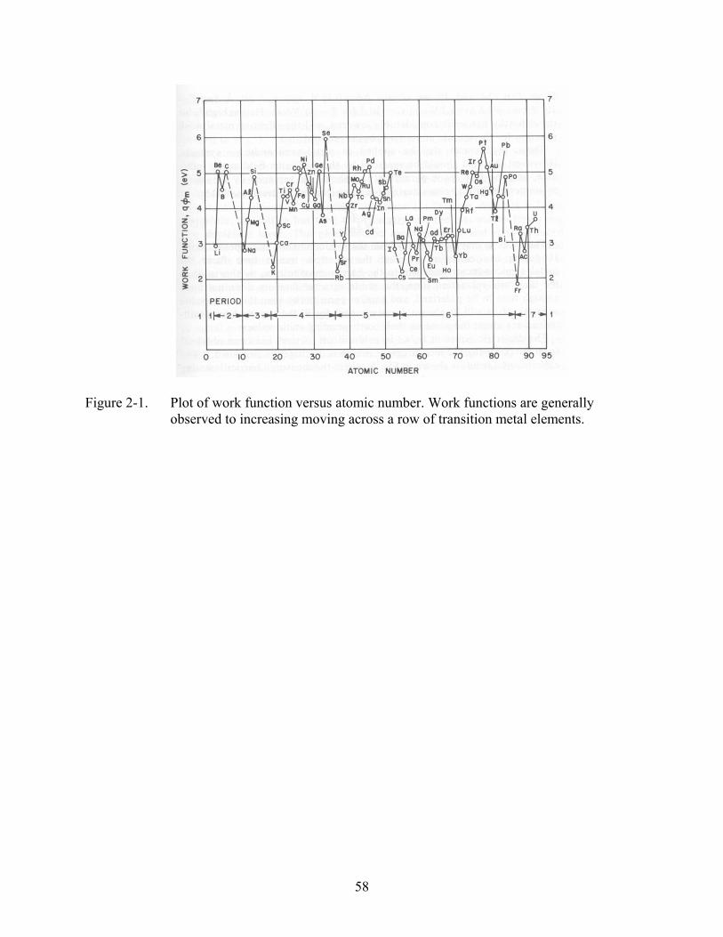
Figure 2-1. Plot of work function versus atomic number. Work functions are generally observed to increasing moving across a row of transition metal elements.
58
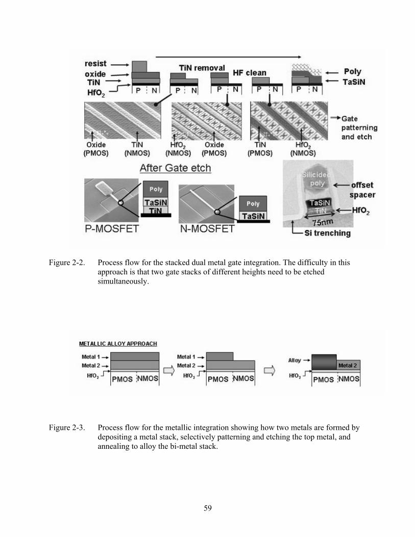
Figure 2-2. Process flow for the stacked dual metal gate integration. The difficulty in this approach is that two gate stacks of different heights need to be etched simultaneously.
Figure 2-3. Process flow for the metallic integration showing how two metals are formed by depositing a metal stack, selectively patterning and etching the top metal, and annealing to alloy the bi-metal stack.
59
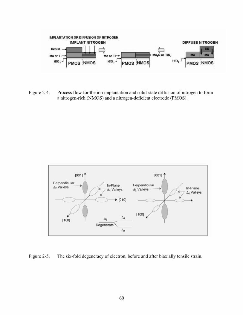
Figure 2-4. Process flow for the ion implantation and solid-state diffusion of nitrogen to form a nitrogen-rich (NMOS) and a nitrogen-deficient electrode (PMOS).
Figure 2-5. The six-fold degeneracy of electron, before and after biaxially tensile strain.
60
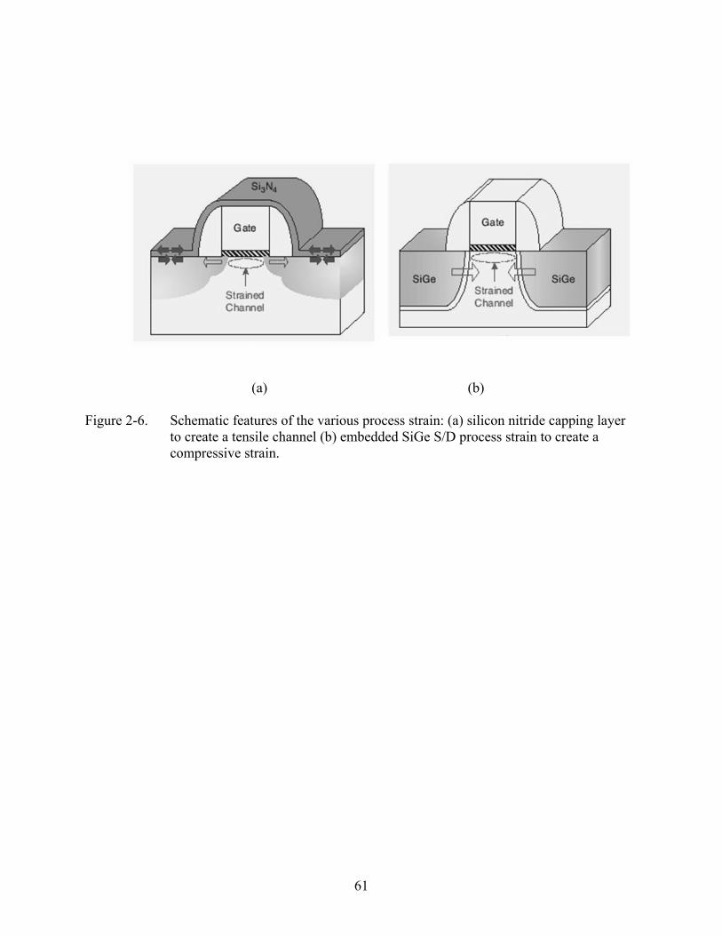
(a) (b)
Figure 2-6. Schematic features of the various process strain: (a) silicon nitride capping layer to create a tensile channel (b) embedded SiGe S/D process strain to create a compressive strain.
61
CHAPTER 3 OUTLINE OF RESEARCH
Keeping all the above mentioned constraints and requirements in mind, the search for an
alternate dielectric requires understanding of material properties of the prospective candidates
and the effects of chemical bonding on the electrical response of the dielectric. With all its
advantages hafnia (HfO2 and Hf-silicate) is still the most promising candidate and this
dissertation is based on the tailoring of Hf-silicate to achieve specific goals such as a medium
dielectric constant (15 – 20), leakage current densities lower than 10-3 A/cm2 at 1 MV/cm and
EOT values around 20 Å and lower. Chapter 4 focuses on the experimental part of this
dissertation. The processing conditions, vacuum science, equipment, sample characterization
techniques and the excimer laser set up along with the UV illumination source are described in
detail. Chapters 5, 6 and 7 describe the results of nitridation process methodologies used to tailor
the properties of hafnia film. Chapter 5 describes the interface degradation within the thermal
nitridation process. In chapter 6 and 7, UV assisted low temperature method for nitridation is
introduced. Chapter 8 and 9 explain the result of Ti based gate electrode properties in order for
dual metal gate application. In chapter 10, since future CMOS device will adopt the strained
MOSFET structure as described above, an effect of mechanical stress on MOS capacitor with
nitrided Hf-silicate dielectric has been studied. Finally, chapter 11 summarizes the research
performed in this dissertation with suggestions for future work to further possibly finetune the
experimentation and data analysis to achieve the goals.
62
CHAPTER 4 EQUIPMENT SET-UP AND CHARACTERIZATION
All the dielectric film samples, studied in this dissertation, were processed via pulsed laser
deposition (PLD). The PLD system was purchased from Neocera Inc, Gaithersburg, MD. The
deposition chamber is equipped with a multi-target carousel, which can hold a maximum of 6
targets. The metal films were initially deposited on p-Si substrates by pulsed laser ablation of
high purity targets (Hf, Ti and Si) from SCI Engineered Materials. The metal films were
subsequently oxidized in high purity oxygen ambient under the presence of ultra-violet (UV)
illumination from a low pressure-vacuum compatible Hg lamp array. The lamps were warmed up
for two minutes prior to the oxidation anneal. The substrate temperature was monitored by a
thermocouple and an optical pyrometer. The gases used in the experiments were high purity
oxygen and ammonia.
Laser System
A Lambda Physik LPX 305 i (KrF) excimer laser (s/n 9412-E-4188) was used for all laser
ablation experiments. The laser works on a pulsed mode delivering 25 nanosecond duration
square wave shaped pulses at frequencies ranging from 1-50 Hz and output energies from 10-
1100 mJ (fluence 0-3 J/cm2). The laser operation is controlled and triggered by a computer and
the mode of trigger can be “internal” or from a remote “external” computer.
Excimer lasers are nowadays commonly used in semiconductor manufacturing and in eye
surgery. Excimer actually refers to an “Excited Dimer”. Most "excimer" lasers are of the noble
gas halide type, for which the term excimer is strictly speaking a misnomer (since a dimer refers
to a molecule of two identical or similar parts). The final output wavelength of the laser is
dependent on the type of gases used. The KrF excimer laser shoots pulses around 254 nm, which
is in the ultra-violet regime. Laser action in an excimer molecule occurs because it has a bound
63
(associative) excited state, but a repulsive (disassociative) ground state. This is because noble
gases such as xenon and krypton are highly inert and do not usually form chemical compounds.
However, when in an excited state (induced by an electrical discharge), they can form
temporarily bound molecules with themselves (dimers) or with halides (complexes) such as
fluorine and chlorine. The excited compound can give up its excess energy by undergoing
spontaneous or stimulated emission, resulting in a strongly-repulsive ground state molecule
which very quickly (on the order of a picosecond) disassociates back into two unbound atoms.
This forms a population inversion between the two states. In the case of our laser, the Kr and F
species are elevated to excited states by application of very high voltages (16 - 21 kV) so that
excited KrF* species are formed. The excited species owing to their extremely short residence
time in the excited state, decay to ground state and in the process photons corresponding to a
wavelength of 254 nm are emitted. As a result of specific cavity design, conditions exist whereby
stimulated emission of coherent radiation occurs and subsequent amplified high-energy laser
output in a pulsed mode can be obtained.
The laser radiation emitted from the cavity is directed towards the deposition chamber
through a variety of optics – an aperture, beam reflectors and final focus lens, before it finally
ablates the target of choice in the chamber, which is pumped to a medium-high vacuum. The
ablation spot on the target had the dimensions of 2 × 5 mm in a nearly perfect representation of
the rectangular aperture used earlier in the beam path. This type of spot was achieved by
adjusting the focusing lens position to a local greater than the focal point of 25 cm to a position
of ~35 cm, which coincided with the image plane of the lens. Owing to the use of an aperture,
imaging of the beam was possible and a spot with a highly uniform energy density was obtained.
64
Pulsed Laser Ablation via Excimer Lasers
In the last two decades, pulsed laser deposition (PLD) has emerged as one of the most
commonly used research tools for oxide thin film processing. The technique has a lot of
advantages with low capital investment, stoichiometric transfer of material from target to
substrate, easy operation, lower vacuum requirements when compared to MBE, effective
prototyping of many different materials being main highlights of this technique. The ablation
process can be explained by the input of energy (incident) from the laser to the target material of
choice. The total incident energy is a summation of
E = Er + Ed + Ep + Ec (3-1)
E = incident energy
Er = reflected energy
Ep = plasma plume energy
Ec = energy absorbed by the cavity wall
Ed = energy of disintegration
For ablation to occur, the pulse or input laser energy should be higher than the bond
strength or energy of the material to be ablated. In short, the combination of pulse energy and
ablation threshold energy determines whether or not material ablation is possible and along with
the degree of ablation. If the pulse energy is lesser than the threshold energy, there will be no
ablation but the energy is still absorbed and this is helpful for laser annealing experiments.
However, if the energy of incidence is too high, particulate ablation can take place. This is
deleterious for high quality film growth. All the experiments were carried out with an incident
laser energy greater than the ablation threshold but low enough to prevent excessive particulate
ablation.
65
It is well known than metals have a different electronic structure than oxides. Owing to
their high reflectivity, higher energies (~ 900-1000 mJ) are typically employed to achieve
ablation.
Vacuum Chamber, Component and Operation
The pulsed laser depositions performed for this dissertation were done in a Neocera brand
vacuum system. A schematic of our Neocera PLD system is shown in Figure 4-1. The system is
a single chamber design that is routinely backfilled with nitrogen gas to atmospheric pressure so
that samples may be mounted or removed. Vacuum levels of 1 × 10⁻⁵ Torr and 1 × 10⁻⁶ Torr
were easily achieved within 3 and 6-7 hours respectively. The chamber is connected to a Pfeiffer
MD-4T oil free diaphragm roughing pump and a Pfeiffer TMU 230 turbo pump. A calibrated
Neocera brand stainless steel resistive heater capable of reaching temperatures around 850 oC is
mounted vertically in the chamber and used to controllably heat and cool the substrate to and
from a desired temperature. The studies performed in this dissertation were done under a base
pressure of 1 10-5 Torr or under 1 × × 10-2 Torr of high purity NH3 during nitridation to
incorporate nitrogen. The chamber has a computer controlled multi-target carousel. Up to 6
targets can be loaded for multi-layer or super lattice depositions. An array of Hg lamps has been
added to the chamber to perform ultraviolet assisted PLD experiments. Four Hg lamps emit a
majority of UV radiation (~240 nm) and a small portion (~ 10 %) of in the 183 nm range. The
Hg lamps are composed of a fused silica envelope with allow more than 85 % of the emitted 183
nm radiation to be transmitted. This 183 nm is mainly responsible for conversion of oxygen into
ozone and other reactive species. Figure 4-2 shows a picture of the UV lamp set up in our
Neocera PLD system. Ultra-pure gases may be added to the system through a highly sensitive
Varian brand leak valve for a wide range of deposition ambients and pressures.
66
Atomic Layer Deposition
Traditionally gate silicon dioxide has been grown and then ntireded, DRAM capacitor
dielectrics have been deposited by Chemical Vapor Deposition (CVD). Problem with thickness
control and uniformity generally limit CVD process to films thicker than 10nm. As addressed in
previous section, the gate oxide thickness of future CMOS device should be less than 10 nm.
Therefore, the need for new deposition technologies is apparent.
Deposition Mechanism
In a “standard” CVD process a wafer or a group of wafers are placed in a vacuum chamber
where chemical vapors are thermally reacted at low pressure to deposit a film on the wafer. The
deposition process is continuous – the vapors flow continually into the chamber during the
deposition cycle. The deposited film thickness depends on the temperature, pressure, gas flows
volumes and uniformity., chemical depletion effects and time ( for state of the art processes
batch systems generally no longer used due to the difficulty of achieving temperature and gas
flow uniformity over multiple substrates at the same time). Controlling all of these parameters to
the level required for good thickness control of thin films is very difficult.
Atomic Layer deposition (ALD) deposits films using pulses of gas producing one atomic
layer at a time. Within fairly wide process windows the deposited film thickness is only
dependent on the number of deposition cycles providing extremely high uniformity and thickness
control. The basic deposition process is illustrated in Figure 4-3.
Figure 4-3 illustrates the deposition of zirconium dioxide which deposition sequence is
very similar with hafnium oxide. The deposition steps are:
1) ZrCl4 vapor is introduced into the process chamber.
67
2) The ZrCl4 vapor forms and an adsorbed monolayer on the surface of the wafer.
Although not shown, following monolayer formation the chamber would be purged
of ZrCl4 vapor by an inert gas prior to the next step.
3) H2O vapor is introduced into the chamber.
4) The H2O vapor reacts with the ZrCl4 surface monolayer to produce one
monolayer of ZrO2. Because only a monolayer of ZCl4 exists on the wafer surface,
only one monolayer of ZrO2 is produced making the process self limited.
Following ZrO2 formation the chamber would be purged again and additional
cycles would be performed as necessary to produce the desired film thickness.
ALD reactions are typically carried out in the 200 oC to 400 oC temperature range. If the
deposition temperature is too high, chemical bonding cannot be sustained or the density of
chemically reactive sites is reduced- reducing deposition rates. If the deposition temperature is
too low thermally activated chmisorption and film forming reaction rates decrease reducing
deposition rates. As the deposition temperature is increased form low to high the deposition rate
increase –reaches a peak and then decreases. The temperature window for maximum deposition
rate is relatively wide compared to CVD processes that are much more temperature sensitive.
Figure 4-4 schematically illustrates the allowable temperature window for ALD.
Precursors must be volatile and thermally stable to ensure efficient transportation so that
reactions will not be precursors transportation controlled. The vapor pressure of precursors must
be high enough to completely fill the deposition chamber so that the monolayer deposition takes
place within a reasonable length of time. Precursors must chemisorb onto the surface or rapidly
react with surface groups and react aggressively with each other to keep deposition times short.
68
The precursor cannot self-decomposes or the self limiting property of ALD is lost and the
precursors should not etch or dissolute into the film or substrate.
Figure 4-5 shows a schematic diagram of deposition cycle of ALD HfSiOx. As shown in
Figure. 4-5, one cycle of ALD HfSiOx (m+n) is composed of m cycles of HfO2 and n cycles of
SiO2. It is possible that compositional control of HfSiOx is achieved by controlling the ratio of
the deposition cycle of HfO2 (m) and SiO2 (n). Very slow ALD SiO2 (m=0) deposition (< 0.1
Å/cycle) was observed with sequential exposure of Si precursor and H2O. However, ALD
HfSiOx films were successfully deposited over 0.5 Å /cycle where the m and n have the
intermediate values between 1 and 10 (1≤ m ≤10 and 1≤ n ≤10).
Wafer Bending Experiment
The uniaxial jig used in applying stress is a four point bending fixture. Figure 4-6 shows a
uniaxial jig. Such a bending structure has been well studied and a relation between the applied
force and stress under uniform stress is given by 89
2
)(3 DLF −=σ
wt (3-2)
where F is the applied force, D and L are the inner and outer support distances respectively,
and w and t are the sample’s width and thickness as shown in Figure 4-7. This formula is
accurate when the sample is not severely bent to the applied forces and the dimensions w and t
are small enough compared with D and L.89 Under these conditions, the stress directions applied
on the both surfaces of the sample can be approximated to be tangential, and the magnitude of
stress applied everywhere between the inner supports can be treated as a constant. A detailed
diagram is shown in figure 4-7. Eq. (3-2) is a useful formula in calibrating stress sensors.89,90
However, we can not use it to directly relate the jig parameters with the measured physical
quantities.
69
Another form of Eq. (3-2) fit for our experiments is found in some literatures 91:
⎟⎠⎞
⎜⎝⎛ −
⋅⋅=⋅=
32
22 aLa
dtYY εσ (3-3)
Here, s and e are the stress and strain values at the center of the sample respectively, Y is
Young’s modulus of Si along the stress direction, 2
DLa −= , and the deflection d is the vertical
displacement between the upper and lower plates of the uniaxial jig when we apply stress. In
figure 4-7, d is defined as d = di - df, and actually measured by the change in micrometer
graduations.
Material and Chemical Characterization Techniques
The as-deposited and annealed films were subjected to a variety of material and chemical
analysis techniques. Information about density, chemical bonding, chemical composition and
microstructure were extracted from the results obtained by the techniques. A brief description of
the material and chemical techniques is given below.
X-ray Reflectivity
X-ray reflectivity (XRR) measurements were made using a PANalytical X’Pert system.
Data generated from an x-ray reflectivity plot include film thickness, roughness and density of
the material under inspection. This technique is very well suited for smooth thin films and is very
sensitive to samples in the 20 – 400 nm range. This technique works by impinging the sample
with x-rays over an array of angles ranging from slightly sub-critical angles to the first few
degrees after the critical angle. The critical angle also known as Brewster’s angle corresponds to
the point at which x-rays change from total reflection off the sample surface to absorption and
interaction with the sample as defined by Snell’s law. The retrieved data results form monitoring
the intensity of the x-ray beam reflected from various interfaces relative to the incident beam as a
70
function of the scattering transfer vector. Fresnel equations will then describe the interaction of
the x-rays with one another and with the interfaces encountered in the film stack. The
constructive or destructive interference nature of the x-rays at a given angle results in the
generation of a fringe pattern. Figure 4-8 shows a typical XRR plot. The generated XRR
spectrum is modeled with a theoretical fit with a model comprising of the different layers in the
sample. For all the samples in this dissertation, a 4-layer model was employed. The layers
include (from substrate and going up) 1) Substrate – silicon in this case 2) Interfacial layer (IL)
formed at the film – Si interface 3) the deposited film 4) Surface contamination layer comprising
of sub-stiochiometric organics as all the samples contain This technique can generate important
information when employed to characterize high k as almost all of the high k films when
deposited on Si form an interfacial layer. The film and interfacial layer – thickness & density can
be obtained from the fit and hence information about the nature of the interface of the film stack
can be deduced from those parameters. However, the better the theoretical model, the more
accurate will the results match the real physical structure.
X-ray Photoelectron Spectroscopy (XPS)
XPS is a photon in-electron out technique based on the ionization of inner shell (core) level
electrons by a monochromatic photon source. The samples in this dissertation were analyzed
using a Perkin Elmer 5100 equipped with Mg Kα radiation source (1253.5 eV). When a sample
is illuminated by a monoenergetic soft x-rays (Mg Kα), the process of photoelectric effect causes
inner shell electrons with kinetic energies ~ 0 – 1500 eV to be emitted. The emitted
photoelectrons have a short mean free path (top few atomic layers) and hence XPS is a highly
surface sensitive technique. The number of photoelectrons emitted are measured based on their
kinetic energy by an electron analyzer. This results in the characteristic photoelectron spectrum
as shown in Figure 4-9. The photoelectron yield in the Y-axis is normally plotted against the
71
binding energy (BE). The kinetic energy is the energy possessed by the photoelectron after
subtracting the energy required to overcome the work function. Each orbital is associated with a
signature binding energy. Thus the photoelectron spectrum can be used to analyze the type of
bonding and elemental composition in the films based on the binding energy of the characteristic
orbital. To analyze the layers at a depth, Angle Resolved X-ray Photoelectron Spectroscopy
(AR-XPS) is normally used where the photoelectrons emanating at various escape angles are
analyzed. Hence, scans at various take off angles (150, 300 and so on) are performed. The 150
scan is surface sensitive while the 900 scan can be used to analyze the chemical environment in
the bulk of the film (in depth). XPS uses photo-ionization and energy dispersive analysis for
chemical composition analysis and study of electronic surface states.
High Resolution Transmission Electron Microscopy (HR-TEM)
Transmission electron microscopy is one of the most powerful microstrucural analysis
techniques available. By this technique we can determine defects in films and achieve atomic
imaging of the interfaces in addition to the regular microstructure analysis. The interfacial layer
abruptness, microstructure and thickness confirmations were performed using a JEOL 2100. One
of the main drawbacks of HR-TEM measurements is the intensive sample preparation required to
obtain high quality images. The sample has to be made extremely thin (~ 80-100 nm) for
electron transparency purposes. A focused ion beam was used to fabricate TEM samples to the
required thicknesses instead of the conventional ion milling process. Figure 9-3 shows a typical
HR-TEM micrograph showing the film microstructure and interfacial layers.
Auger Electron Spectroscopy (AES)
AES is a popular technique for determining the composition of the top few layers of a
surface. It cannot detect hydrogen or helium, but is sensitive to all other elements, being most
sensitive to the low atomic number elements. The electron beam can be focused over a large or
72
small surface area, or it can be directly focused on a small surface feature. This ability to focus
the electron beam to diameters of 10 nm and less makes AES an extremely useful tool for
elemental analysis of small surface features. Moreover, the ability to raster the electron beam
over an adjustable surface area provides control over the size of the analytical area. When used
in combination with ion sputter sources, AES can perform large- and small-area compositional
depth profiling. Despite the advantages of high spatial resolution and precise chemical sensitivity
attributed to AES, there are several factors that can limit the applicability of this technique,
especially when evaluating solid specimens. One of the most common limitations encountered
with Auger spectroscopy are charging effects in non-conducting samples. Charging results when
the numbers of secondary electrons leaving the sample are greater or less than the number of
incident electrons, giving rise to a net polarity at the surface. Both positive and negative surface
charges severely alter the yield of electrons emitted from the sample and hence distort the
measured Auger peaks. To complicate matters, neutralization methods employed in other surface
analysis techniques, such as secondary ion mass spectrometry (SIMS), are not applicable to AES,
as these methods usually involve surface bombardment with either electrons or ions (i.e. flood
gun).
In this work, to confirm the chemical intermixing between metal and dielectric film with
respect to the PDA temperature, AES depth profile analysis was conducted using a Physical
Electronics 660 Scanning Auger Microprobe. The electron beam conditions were 10 keV, 1 mA
beam current at 45o from sample normal.
Secondary Ion Mass Spectroscopy (SIMS)
SIMS depth profiles were acquired with a Perkin-Elmer PHI 6600 SIMS system using a
1keV cesium primary ion beam with negative and positive secondary acquisition. The current
73
intensity was set at 32 nA. The raster size was 450 × 450µm2 with 70% gating during negative
secondary acquisition and 55 % gating with positive secondary acquisition.
Under Cs bombardment, nitrogen has to be detected combined with an impurity ion or
another species in the matrix. With negative secondary acquisition, N was acquired as mass
43SiN-. Characterization of these films with negative secondary acquisition has one drawback:
mass interferences (i.e. secondary ions that occur at the same nominal mass). Mass interferences
occur whenever an isotope of one element has the same nominal mass as an isotope of another.
Isotopes of one element, dimers, and molecular combinations may also have the same nominal
mass as others.
Positive secondary acquisition using CsX+ cluster ions, where X is the impurity element of
interest has less matrix effects but the intensity of the signals is much lower than with negative
acquisition. Nitrogen was monitored using 147CsN+. Oxygen, Si, and Hf were monitored using
149CsN+, 161CsSi+, and 180CsHf+, respectively.
This SIMS data is only qualitative. SIMS is used for detection of minor impurity elements
(less than 1%in the matrix) and quantification of impurities requires the analysis of standards
under the same instrumental conditions as the unknowns. This is because SIMS is a very matrix
dependent technique, that is, the sensitivity of the same element varies with matrix composition.
Standards can be either implants or bulk-doped samples with known concentrations of the
species of interest in exactly the same matrix as the unknown samples. When standards are not
available, the levels of the impurities of interest can be compared between samples after ratioing
the intensity of the impurity of interest to a constant matrix ion.
Electrical Characterization
The quality of the dielectric films can be analyzed and confirmed by the use of electrical
characterization techniques such as capacitance-voltage (C-V) and current-voltage (I-V) methods.
74
After the dielectric film deposition and material analysis (XRR, XPS etc), metal oxide
semiconductor (MOS) devices were fabricated by depositing Pt dots of known areas on the
dielectric by R.F sputtering. The typical thickness of the dots was around 900 Å. Silver was used
as the backside contact. The Pt dots were deposited via a shadow mask with an array of circular
dots ranging from 25 – 500 μm diameter were used to create the dot arrays on the samples. The
dot size used for analysis in this dissertation was 3.16 × 10⁻⁴ A/cm2. It is important to choose the
appropriate metal for the contacts. If improper metals are chosen, band alignments may exist
whereby the nonohmic contacts are created within the device itself. As an example, the backside
contact on a p-Si wafer should have a workfunction greater than that of Si. If not, the contact will
be a Schottky contact (rectifying). After the deposition of contacts was completed, the samples
were annealed in forming gas (95 % N2 and 5 % H2) at 450 oC for 30 minutes in a conventional
furnace. This is mainly done to passivate the dangling bonds that might exist at the gate-
dielectric and dielectric-Si interfaces. Both current-voltage and capacitance-voltage
measurements were conducted after the forming gas annealing process.
Current-Voltage Measurements
Once the MOS capacitors structures were fabricated, a Keithley Instruments Inc., K1236
source measurement unit (SMU) was used to measure the current flow through the device. The
236 SMU was attached to a black box probe station equipped with a pair of Signatone Inc,
micromanipulators. The manipulators were fitted with tungsten probes that were milled to
produce a fine ~ 5 μm tip. The output of the SMU was connected to the micromanipulator in
contact with the gate (Pt) while the input was connected to the backside contact (Ag). This
configuration is optimal for the determination of current leakage pathways directly below the
device being measured (i.e, it avoids stray leakage paths). Determination of the leakage current is
an important step in analyzing the quality of the MOS device. Typically the current compliance
75
threshold (a value that may not be exceeded) of 100 nA is fed into the measurement parameters.
Then a direct current bias sweep is conducted over a voltage range and the amount of current that
passes through the MOS structure is monitored. Typically, it is best to start at a small voltage
sweep range so that it is possible to determine if the device is leaky without causing a large
amount of bias induced defects. The main goal of the leakage current measurements is to identify
a high quality MOS device that can be used for capacitance-voltage measurements to extract
parameters such as capacitance, dielectric constant and equivalent oxide thickness (EOT).
Capacitance-Voltage Measurements
Capacitance-voltage measurements serve as one of the most versatile and sensitive of all
electrical techniques. It is the ultimate tool for determining discreet differences in a MOS device
that may serve as a final word in whether a given processing condition has resulted in a high
quality device. The measurements in this dissertation were carried out with a Keithley
Instruments Inc. Win-82 measurement set-up. This system is comprised of four main
components that work in unison. The Keithley 590 capacitance meter is used for high frequency
capacitance measurements at 100 KHz and 1 MHz. The Keithley 595 capacitor meter was used
for simultaneous quasistatic low frequency measurements. The Keithley 230 voltage source is
used for static bias condition measurements. These three devices were wired into the Keithley
5951 remote input coupler, which serves to filter the device data to and from the various pieces
of equipment.
The output of a typical C-V curve is shown in figure 4-10. There are several important
features that should be noted. First, there are three important regions with respect to gate bias
voltage to take into consideration, known as accumulation, depletion and inversion. The presence
of the different regions is a result of majority charge carriers in the semiconductor. When a
negative bias is applied to the gate electrode, positively charged holes are attracted from the bulk
76
of the semiconductor to the oxide – semiconductor interface region where they accumulate
(accumulation). The depletion region is generated when a gate is made less negative and the
reduced field across the oxide causes the charge at the interface to diminish. As the sign on the
voltage changes from negative to positive, majority carriers are repelled from the interface
creating an area depleted of majority carriers (depletion region). Finally, the inversion region is
generated when the voltage becomes very positive and the depletion width has increased to a
point where the other mechanisms may become important. For example, in the depletion region,
the product of the concentration of electrons and holes (np) is much less than the square of the
intrinsic carrier concentration (ni2) and in this case, pair generation may occur and the subsequent
minority carriers may migrate to the oxide-semiconductor interface. Further depletion is
prevented due to screening effect of the minority carriers.
77
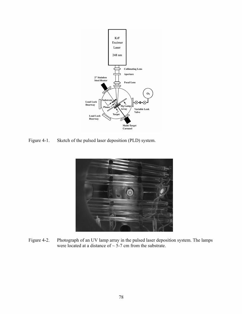
Figure 4-1. Sketch of the pulsed laser deposition (PLD) system.
Figure 4-2. Photograph of an UV lamp array in the pulsed laser deposition system. The lamps were located at a distance of ~ 5-7 cm from the substrate.
78
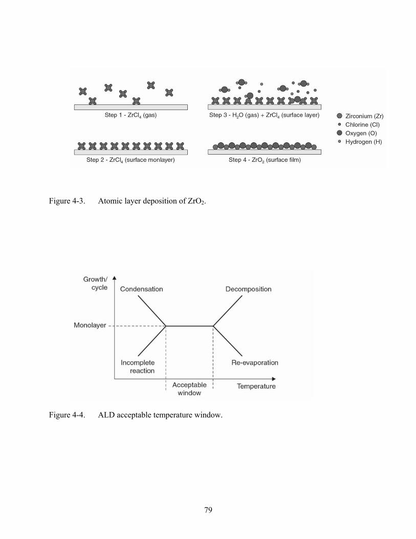
Figure 4-3. Atomic layer deposition of ZrO2.
Figure 4-4. ALD acceptable temperature window.
79
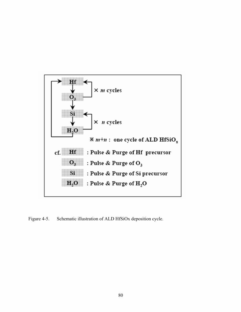
Figure 4-5. Schematic illustration of ALD HfSiOx deposition cycle.
80
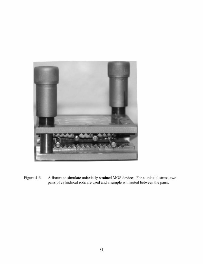
Figure 4-6. A fixture to simulate uniaxially-strained MOS devices. For a uniaxial stress, two pairs of cylindrical rods are used and a sample is inserted between the pairs.
81
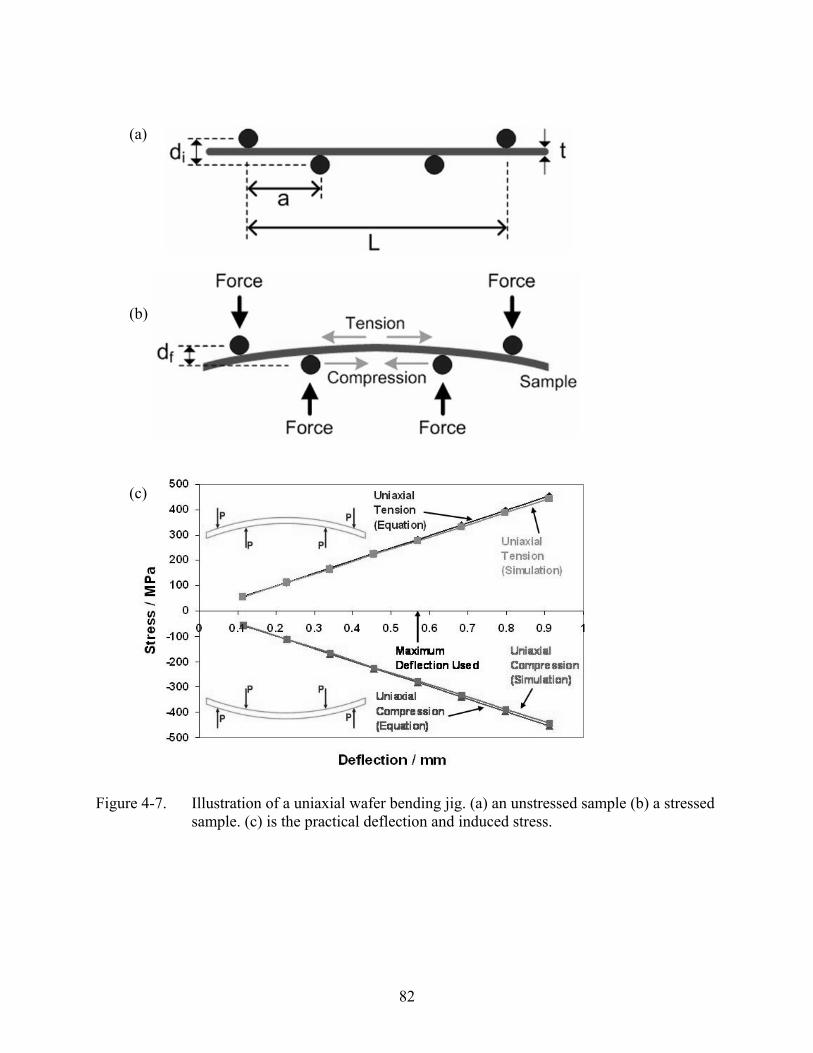
(a)
(b)
(c)
Figure 4-7. Illustration of a uniaxial wafer bending jig. (a) an unstressed sample (b) a stressed sample. (c) is the practical deflection and induced stress.
82
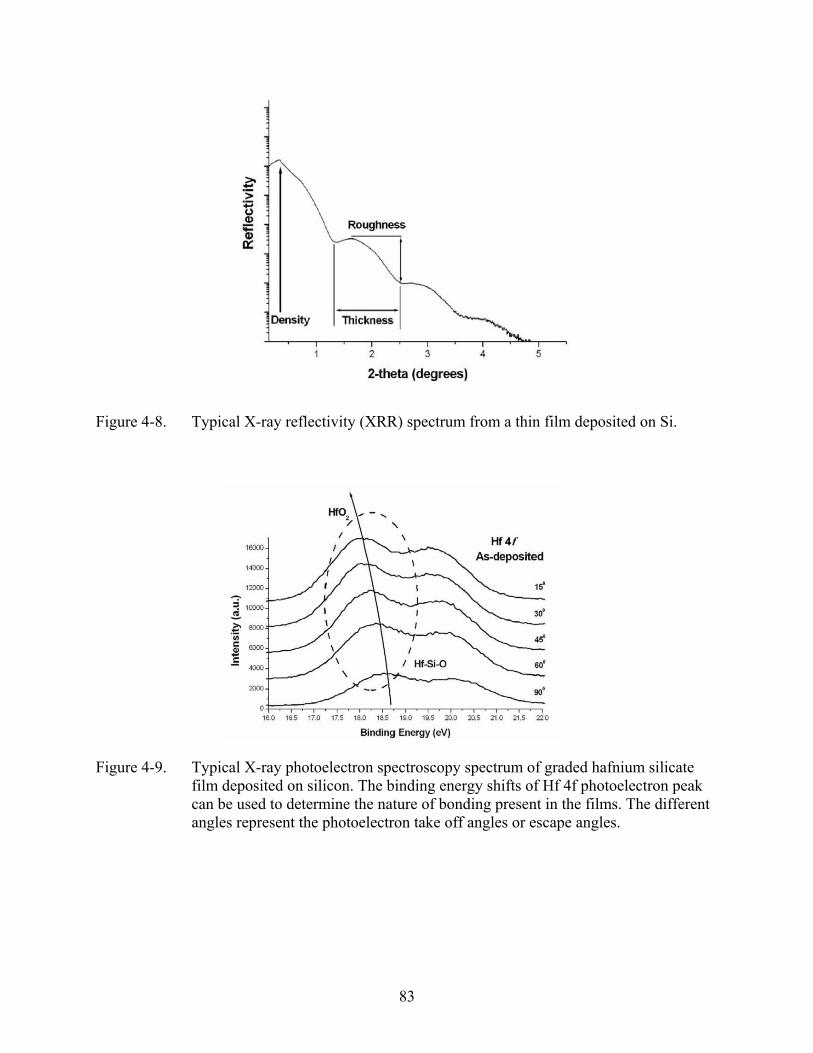
Figure 4-8. Typical X-ray reflectivity (XRR) spectrum from a thin film deposited on Si.
Figure 4-9. Typical X-ray photoelectron spectroscopy spectrum of graded hafnium silicate film deposited on silicon. The binding energy shifts of Hf 4f photoelectron peak can be used to determine the nature of bonding present in the films. The different angles represent the photoelectron take off angles or escape angles.
83
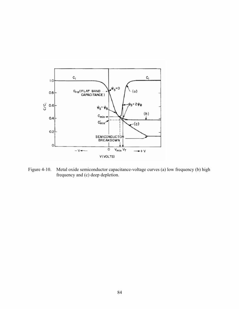
Figure 4-10. Metal oxide semiconductor capacitance-voltage curves (a) low frequency (b) high frequency and (c) deep depletion.
84
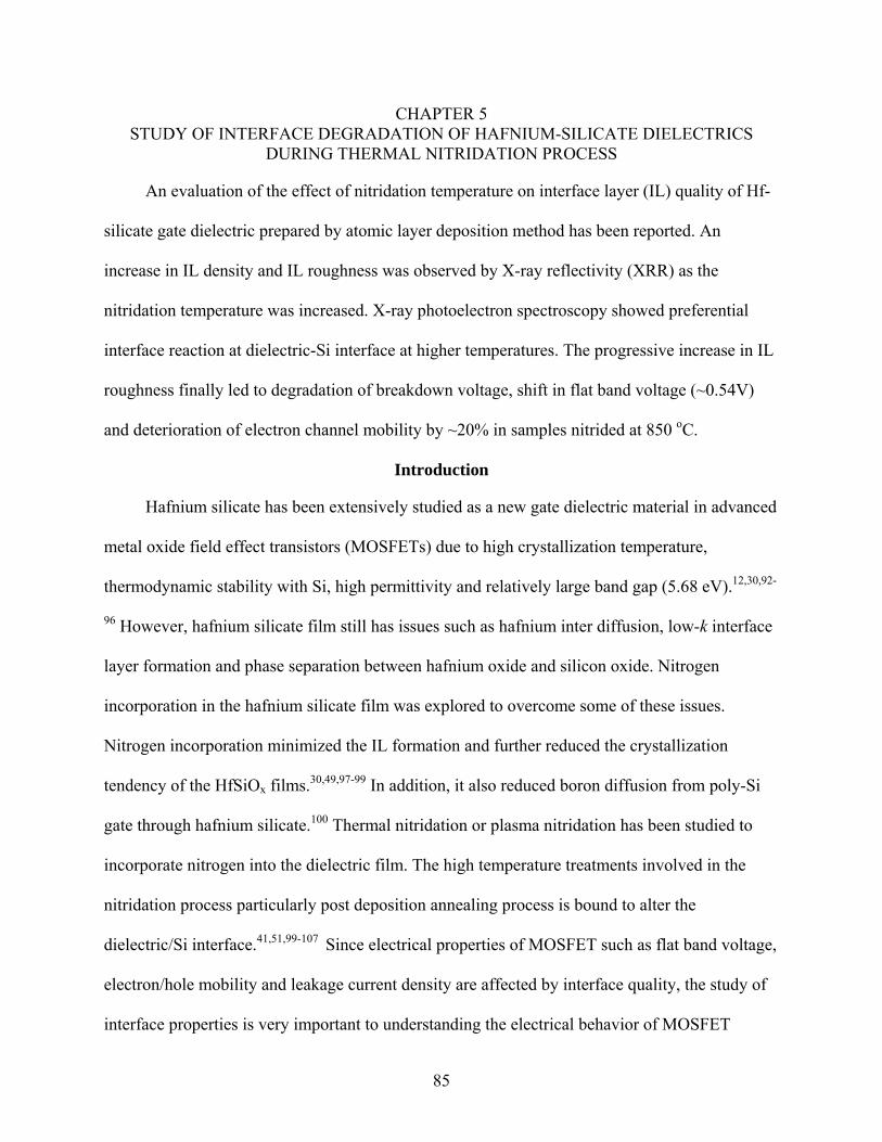
CHAPTER 5 STUDY OF INTERFACE DEGRADATION OF HAFNIUM-SILICATE DIELECTRICS
DURING THERMAL NITRIDATION PROCESS
An evaluation of the effect of nitridation temperature on interface layer (IL) quality of Hf-
silicate gate dielectric prepared by atomic layer deposition method has been reported. An
increase in IL density and IL roughness was observed by X-ray reflectivity (XRR) as the
nitridation temperature was increased. X-ray photoelectron spectroscopy showed preferential
interface reaction at dielectric-Si interface at higher temperatures. The progressive increase in IL
roughness finally led to degradation of breakdown voltage, shift in flat band voltage (~0.54V)
and deterioration of electron channel mobility by ~20% in samples nitrided at 850 oC.
Introduction
Hafnium silicate has been extensively studied as a new gate dielectric material in advanced
metal oxide field effect transistors (MOSFETs) due to high crystallization temperature,
thermodynamic stability with Si, high permittivity and relatively large band gap (5.68 eV).12,30,92-
96 However, hafnium silicate film still has issues such as hafnium inter diffusion, low-k interface
layer formation and phase separation between hafnium oxide and silicon oxide. Nitrogen
incorporation in the hafnium silicate film was explored to overcome some of these issues.
Nitrogen incorporation minimized the IL formation and further reduced the crystallization
tendency of the HfSiOx films.30,49,97-99 In addition, it also reduced boron diffusion from poly-Si
gate through hafnium silicate.100 Thermal nitridation or plasma nitridation has been studied to
incorporate nitrogen into the dielectric film. The high temperature treatments involved in the
nitridation process particularly post deposition annealing process is bound to alter the
dielectric/Si interface.41,51,99-107 Since electrical properties of MOSFET such as flat band voltage,
electron/hole mobility and leakage current density are affected by interface quality, the study of
interface properties is very important to understanding the electrical behavior of MOSFET
85
device. Previous reports have already revealed that engineering IL by nitrogen incorporation
improved the electrical properties of MOS device.95 However, all the above mentioned results
were qualitative studies, there are only a few quantitative reports for interface properties
especially, interface roughness change with respect to the nitridation process. In this chapter, I
focused on quantitative analysis of the interface layer roughness change with respect to the
nitridation temperature by XRR studies and reveal the origin of IL roughness changes by the
investigation of chemical state variation using XPS. Finally electrical characteristics of HfSiOx
films corresponding to the physical properties of IL are examined.
Experimental Detail
HfSiOx films were deposited directly on MEMC p-type (100) pre-cleaned (SC1, 1% HF
solution and DI water rinse) Si substrates with a resistivity of 3-25 Ωcm, by atomic layer
deposition (ALD) using GENUS Lynx2TM at 300oC. SiH[N(CH3)2]3 was used as Si precursor
whereas Hf(NEtMe)4 (TEMAH) was employed as Hf precursor. The oxidizing agents for
TEMAH and Si were O3 and H2O, respectively.18 In order to minimize the dielectric constant
loss of Hf-silicate film, Hf and Si ratio (Hf/Hf+Si) in the film was tuned to 0.9. HfSiOx film
deposition was followed with nitrogen incorporation by rapid thermal anneal in NH3 ambience
for 60 s. Nitridation temperature was varied from 300oC to 850oC. The change in chemical state
was investigated using x-ray photoelectron spectroscopy (XPS) with Mg Kα radiation. Interface
layer (IL) thickness and interface roughness was determined using x-ray reflectivity (XRR,
PANalytical X’pert system). For XRR spectra, an X-ray mirror and parallel plate collimator were
used as the primary and secondary optics, respectively. In order to investigate the electrical
characteristics of films, metal-oxide-semiconductor (MOS) capacitor with Pt gate electrode and
poly Si gate MOSFET was fabricated using oxide mask technique. The C-V characteristics were
analyzed at high frequency (1 MHz) using an HP 4284A LCR meter. NCSU program was used to
86
analyze the electrical measurements and extract the flat band voltage and mobility. The gate
current density-voltage (J-V) and dielectric breakdown (BD) measurements were performed
using HP4156B. The statistical approach for BD behavior was analyzed by using of Weibull
distribution function. The interfacial state density (Dit) at flat band voltage was determined by the
method of Lehovec.104-106
Results and Discussion
X-ray reflectivity (XRR) spectra of Hf-silicate films are presented in figure 5-1. Since
XRR spectra were obtained using the symmetric θ/2θ configuration with very small angles, this
technique is suitable for the investigation and characterization of thin films. From the curve
fitting of periodic pattern width and height, we can find the interface roughness and thickness.
For the best curve fitting (Wingixa software, Philips), a multi-layer model, which consisted of
the interfacial, Hf-silicate, and contamination layers, was applied. Film density was determined
by the critical angle (θc) in which the experimental deviation is about ±3% in our study. The
non-specular diffuse scattering as well as the specular scattering was considered in order to
obtain the surface and interfacial roughness values which we are focusing on in this report. The
physical structure of Hf-silicate dielectric such as thickness, density and roughness of the film
and the IL as obtained from XRR measurement after thermal nitridation is tabulated in Table 1.
It can be observed from table 5-1 that both the film and IL density is increasing with nitridation
temperature. Increase in nitrogen incorporation with increase in the nitridation temperature has
been reported earlier.95 The densification of film and IL can be attributed to the presence of
larger amount of nitrogen. The increase in thickness of IL is due to higher diffusivity of nitrogen
at higher temperatures. It should also be noted that the density of the film is more than twice that
of the IL indicating IL to be mostly Si bonded to O and N.
87
Roughness of the IL is an important property which can affect the interface charge density
and cause scattering of electrons, surprisingly it has not been studied in HfO2, Hf-silicate system
to the best of our knowledge. It is especially important in the case of post deposition nitridation
process (thermal nitridation, plasma nitridation) where growth of IL occurs at high temperatures
and is diffusion controlled. As can be observed from table 1, roughness of the IL is increasing
with nitridation temperature. The increase in nitrogen content in the film is coming at the cost of
degradation of IL/Si interface. This degradation is particularly rapid at nitridation temperatures
of 750 and 850oC as is the case with other properties.
Figure 5-2 (a) shows the effect of nitridation temperature on high resolution XPS scan of
Hf 4f peak region. The Hf 4f7/2 peak for as deposited sample which is predominantly HfSixOy is
at 18.1 eV. The Hf 4f7/2 peak undergoes a shift towards lower binding energy (BE) with increase
in nitridation temperature particularly at temperatures above 650oC. The lowering of BE
indicates an increase in the screening of Hf 4f level, which results from increased electron
density around Hf atom. In case of nitridation, increase in electron density comes from the
incorporation of N atoms having lower electronegativity i.e. by formation of Hf-N-Hf or Hf-N-Si
bonding states.102,103 The continuous shift towards lower BE implies continuously increasing
nitrogen amount in the film with higher nitridation temperature. The broadening of Hf 4f peaks
with the increase in nitridation temperature can also be seen in the figure. Peak broadening is
probably the result of randomization of Hf environment by incorporation of higher percentage of
N atoms.104 Shown in figure 5-2 (b), are the N 1s core level XPS scan and the deconvoluted
spectra of the dielectric films nitrided at different temperatures. A drastic change in the shape of
the peaks with increase in nitridation temperature can be observed, indicating a change in the
nature of N atom bonding. The N 1s spectra of nitrided Hf-silicate films was shown by Cho et al.
88
to be a fusion of numerous peaks 397.0±0.3 eV (N1), 398.1±0.2 eV (N2), 398.7±0.2 eV (N3),
400.0±0.1 eV (N4), and 403.3 eV (N5), each originating from different bonding environment of
N atoms.101,102 The low BE peaks (N1, N2, N3) comes from N atoms bonded mostly to Si atoms,
N1 from plannar structured N≡Si3, N2 differing from N1 with respect to the second nearest
neighbor and N3 peak from O-N=Si2. High BE N4 peak is attributed to N atoms bonded to Hf in
HfO2 matrix.101,102 The N5 peak was assigned to N2 and NOx molecular states which can easily
out diffused at high temperature.101,102 The 300oC nitrided sample showed a major portion of N4
state and existence of N5 peak with minor N1 state. The prominence of Hf bonded N (N4) and
N5 at 300oC can be explained by surface saturation of N atoms due to limited diffusion of N
inside the film. The increase in nitridation temperature to 650oC is marked by (i) increase in the
intensity of N1 peak, (ii) appearance of another Si bonded N3 state and (iii) disappearance of
molecular N2, NOx peaks(N5) from the spectrum. The increase in nitridation temperature will
increase the N diffusion inside the film and to the IL. This led to increase in the thickness of IL
as shown in Table 1. But the disproportionate increase in the intensity of N1 and N2 peaks
compared to the IL growth at 750 and 850 oC nitridation shows a preferential buildup of N at the
interface. The higher affinity of nitrogen to Si compared to Hf is well reported, it seems like Si
interface is acting as a sink for nitrogen during high temperature nitridation. Therefore, the
degraded IL roughness which was observed by XRR measurements, can be understood by the
result of the N inter diffusion and preferential accumulation in the IL. The IL roughness
degradation without film surface roughness change (table 5-1) also ascertains that the IL
roughness degradation was a result of inter diffusion process.
I investigated the electrical properties of the Hf silicate films to determine the structure-
property correlation. The variations in the flat band voltage with nitridation temperature are
89
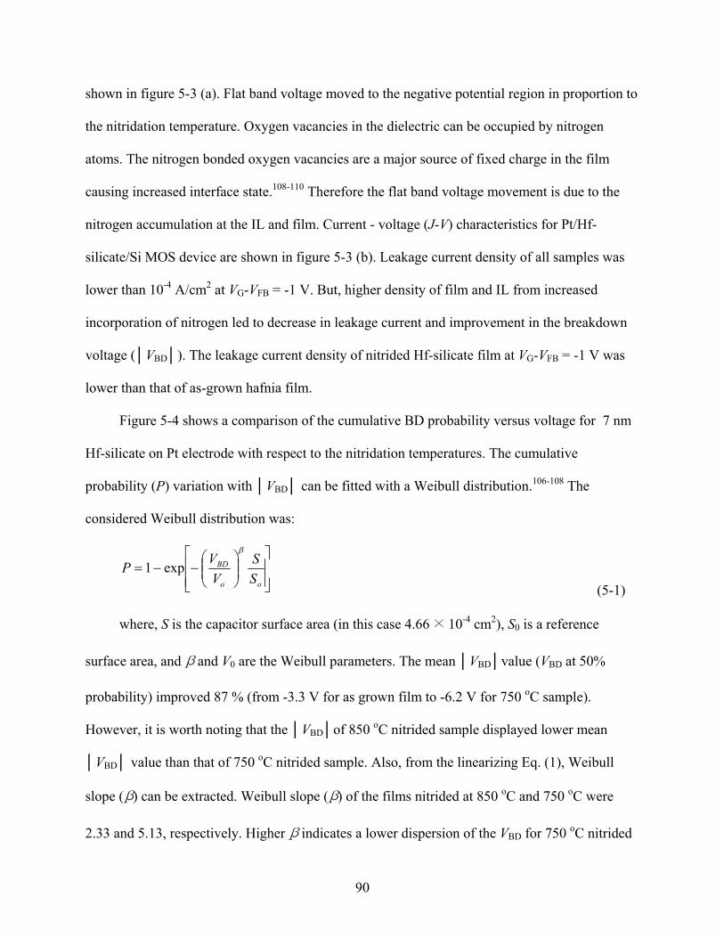
shown in figure 5-3 (a). Flat band voltage moved to the negative potential region in proportion to
the nitridation temperature. Oxygen vacancies in the dielectric can be occupied by nitrogen
atoms. The nitrogen bonded oxygen vacancies are a major source of fixed charge in the film
causing increased interface state.108-110 Therefore the flat band voltage movement is due to the
nitrogen accumulation at the IL and film. Current - voltage (J-V) characteristics for Pt/Hf-
silicate/Si MOS device are shown in figure 5-3 (b). Leakage current density of all samples was
lower than 10-4 A/cm2 at VG-VFB = -1 V. But, higher density of film and IL from increased
incorporation of nitrogen led to decrease in leakage current and improvement in the breakdown
voltage (VBD). The leakage current density of nitrided Hf-silicate film at VG-VFB = -1 V was
lower than that of as-grown hafnia film.
Figure 5-4 shows a comparison of the cumulative BD probability versus voltage for 7 nm
Hf-silicate on Pt electrode with respect to the nitridation temperatures. The cumulative
probability (P) variation with VBD can be fitted with a Weibull distribution.106-108 The
considered Weibull distribution was:
⎥⎥⎦
⎤
⎢⎢⎣
⎡⎟⎟⎠
⎞⎜⎜⎝
⎛−−=
oo
BD
SS
VVP
β
exp1 (5-1)
where, S is the capacitor surface area (in this case 4.66 × 10⁻⁴ cm2), S0 is a reference
surface area, and β and V0 are the Weibull parameters. The mean VBDvalue (VBD at 50%
probability) improved 87 % (from -3.3 V for as grown film to -6.2 V for 750 oC sample).
However, it is worth noting that the VBDof 850 oC nitrided sample displayed lower mean
VBD value than that of 750 oC nitrided sample. Also, from the linearizing Eq. (1), Weibull
slope (β) can be extracted. Weibull slope (β) of the films nitrided at 850 oC and 750 oC were
2.33 and 5.13, respectively. Higher β indicates a lower dispersion of the VBD for 750 oC nitrided
90
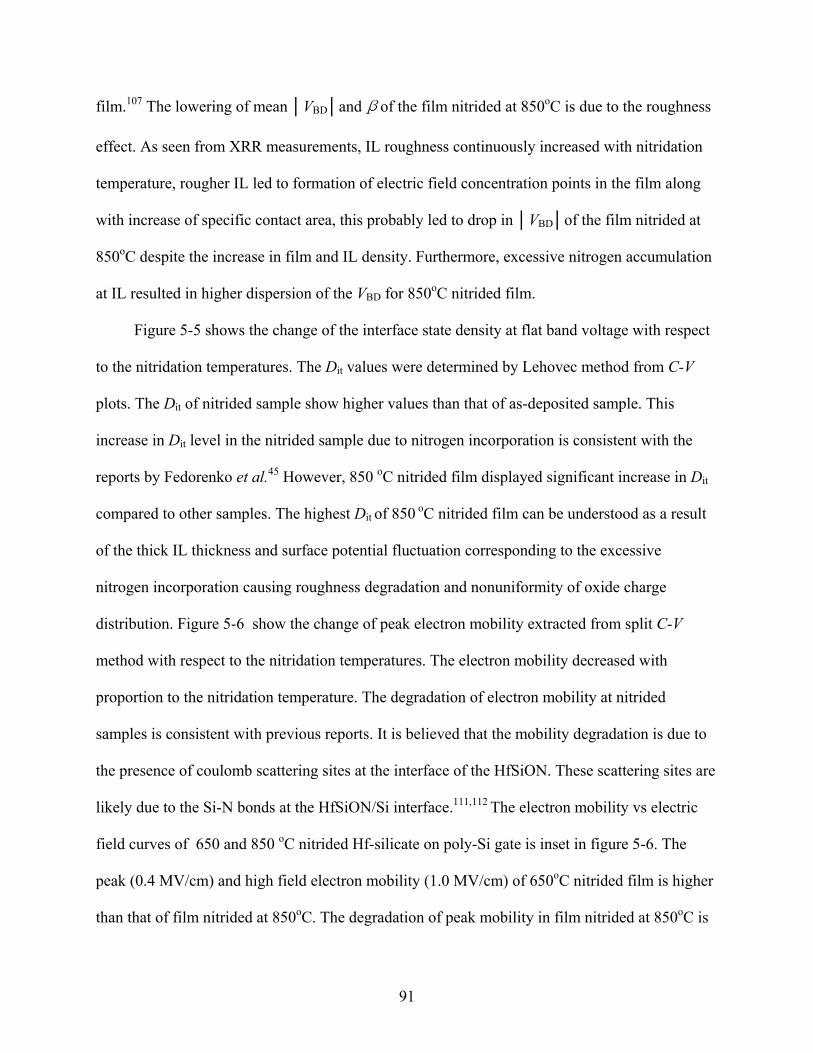
film.107 The lowering of mean VBDand β of the film nitrided at 850oC is due to the roughness
effect. As seen from XRR measurements, IL roughness continuously increased with nitridation
temperature, rougher IL led to formation of electric field concentration points in the film along
with increase of specific contact area, this probably led to drop in VBDof the film nitrided at
850oC despite the increase in film and IL density. Furthermore, excessive nitrogen accumulation
at IL resulted in higher dispersion of the VBD for 850oC nitrided film.
Figure 5-5 shows the change of the interface state density at flat band voltage with respect
to the nitridation temperatures. The Dit values were determined by Lehovec method from C-V
plots. The Dit of nitrided sample show higher values than that of as-deposited sample. This
increase in Dit level in the nitrided sample due to nitrogen incorporation is consistent with the
reports by Fedorenko et al.45 However, 850 oC nitrided film displayed significant increase in Dit
compared to other samples. The highest Dit of 850 oC nitrided film can be understood as a result
of the thick IL thickness and surface potential fluctuation corresponding to the excessive
nitrogen incorporation causing roughness degradation and nonuniformity of oxide charge
distribution. Figure 5-6 show the change of peak electron mobility extracted from split C-V
method with respect to the nitridation temperatures. The electron mobility decreased with
proportion to the nitridation temperature. The degradation of electron mobility at nitrided
samples is consistent with previous reports. It is believed that the mobility degradation is due to
the presence of coulomb scattering sites at the interface of the HfSiON. These scattering sites are
likely due to the Si-N bonds at the HfSiON/Si interface.111,112 The electron mobility vs electric
field curves of 650 and 850 oC nitrided Hf-silicate on poly-Si gate is inset in figure 5-6. The
peak (0.4 MV/cm) and high field electron mobility (1.0 MV/cm) of 650oC nitrided film is higher
than that of film nitrided at 850oC. The degradation of peak mobility in film nitrided at 850oC is
91
correlated with the result of Dit degradation which can be a coulomb scattering center.111,112
However, it should be noted that the difference in electron mobility of film nitrided at 650 and
850oC is larger at high electric field than at the field of peak mobility. The mobility degradation
at high field can be understood as a result of the IL roughness degradation caused by excessive
nitrogen piling up effect.
Conclusions
The effect of temperature in thermal nitridation process on physical structure of the IL was
investigated using XRR studies. At high nitridation temperatures, the nitridation efficiency
increased leading to increase in IL roughness apart from increase in film and IL density and IL
thickness. There was a general improvement in the electrical properties of films at higher
nitridation temperature till the degradation of interface quality due to interface roughening led to
degradation of some of the electrical properties. An excessive nitrogen piling up at IL of 850 oC
nitrided Hf-silicate resulted in nonuniform distribution of nitrogen and oxide charge, high
roughness IL and degradation of Dit, electron channel mobility and breakdown resistance.
Therefore, the quantitative results of IL roughness by XRR study showed reliable
correspondence with electrical results and can have a potential as an analysis tool of thin film
structure.
92
Table 5-1. Summary of x-ray reflectivity data on roughness, density, and thickness of IL and HfSiNO films.
Figure 5-1. The comparison of XRR patterns with respect to the nitridation temperature.
93
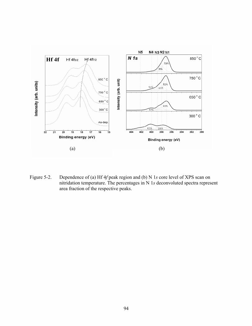
(a) (b)
Figure 5-2. Dependence of (a) Hf 4f peak region and (b) N 1s core level of XPS scan on nitridation temperature. The percentages in N 1s deconvoluted spectra represent area fraction of the respective peaks.
94
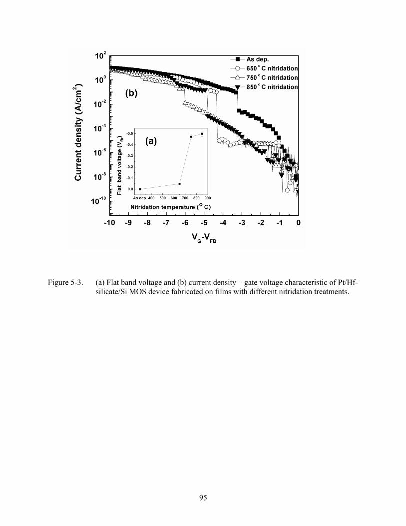
Figure 5-3. (a) Flat band voltage and (b) current density – gate voltage characteristic of Pt/Hf-silicate/Si MOS device fabricated on films with different nitridation treatments.
95
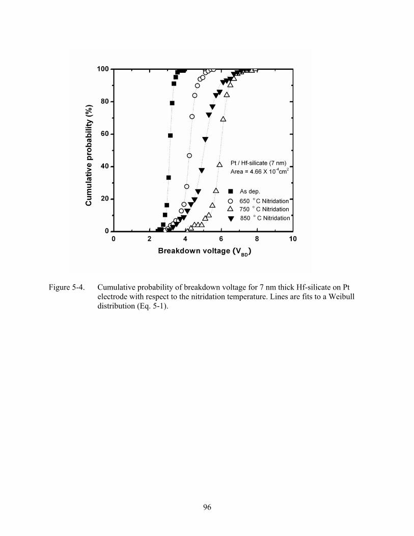
Figure 5-4. Cumulative probability of breakdown voltage for 7 nm thick Hf-silicate on Pt electrode with respect to the nitridation temperature. Lines are fits to a Weibull distribution (Eq. 5-1).
96
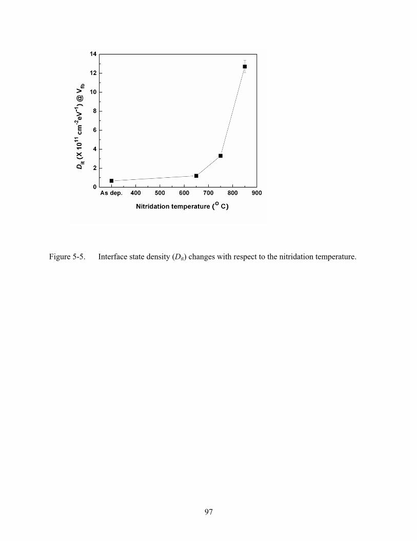
Figure 5-5. Interface state density (Dit) changes with respect to the nitridation temperature.
97
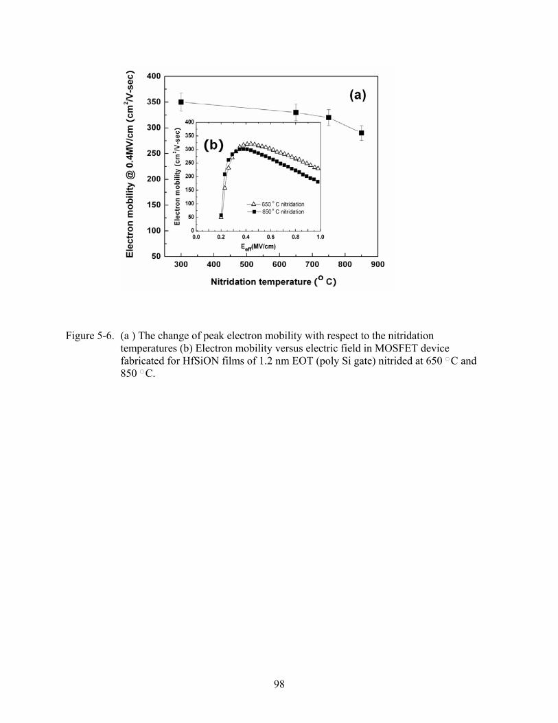
Figure 5-6. (a ) The change of peak electron mobility with respect to the nitridation temperatures (b) Electron mobility versus electric field in MOSFET device fabricated for HfSiON films of 1.2 nm EOT (poly Si gate) nitrided at 650 C and 850 C.
98
CHAPTER 6 HIGH EFFICIENCY NITROGEN INCORPORATION TECHNIQUE USING UV ASSISTED
LOW TEMPERATURE PROCESS FOR HAFNIA DIELECTRICS
An evaluation of a low temperature process (~350 oC) for nitrogen incorporation in hafnia
gate dielectric has been reported. This method is based on post-deposition nitridation under
ultraviolet light illuminated NH3 ambience. X-ray photoelectron spectroscopy confirmed the
amount of nitrogen incorporated by this process was comparable to that of high temperature
(~650 oC) thermal nitridation (~7%). Uniformity of nitrogen distribution in the film was
analyzed by secondary ion mass spectroscopy. A capacitance density of ~ 3.96 µF/cm2 with 9.4
Å equivalent oxide thickness and 10 Å thick interface layer were obtained by ultraviolet assisted
nitridation process
Introduction
Hafnium silicate has been extensively studied as an alternative gate dielectric material in
advanced metal oxide field effect transistors (MOSFETs) due to high crystallization temperature,
thermodynamic stability with Si, high permittivity and relatively large band gap (5.68 eV). 30,92-
96,113. However, hafnium silicate film still has issues such as hafnium inter diffusion, low-k
interface layer (IL) formation and phase separation between hafnium and silicon oxides.
Nitrogen incorporation in hafnium silicate was explored to enhance the resistance to thermal
degradation. Nitrogen incorporation minimized the IL formation and further reduced the
crystallization tendency of the HfSiOx films.30,114-117 In addition, it also reduced boron diffusion
from poly-Si gate through hafnium silicate.48 However, most of the nitrogen incorporation
methods employ post deposition annealing process such as rapid thermal annealing ( RTA ) in
NH3 or N2O ambience at high temperatures ( > 650 oC). As a result of high temperature
nitridation process, additional interface degradation such as low-k oxide layer growth and boron
diffusion have been observed.116,117 Hence, to reduce the total heat budget during device
99
integration, there is a critical need to explore a low temperature nitrogen doping method which
has comparable efficiency as high temperature methods in order to minimize interface
degradation.
As ultraviolet (UV) light irradiation has been reported to create highly reactive species by
photochemical dissociation process,48,118-121 UV assisted nitridation method was thought to have
the potential to lower the incorporation process temperature. In this chapter, I introduce low
temperature nitrogen incorporation method using UV illumination and thereafter compare the
interface properties, incorporation efficiency and electrical performance with thermal nitridation
process.
Experimental Detail
HfSiOx films were deposited directly on p-type (100) pre-cleaned (1% HF solution and DI
water rinse) Si substrates, by atomic layer deposition (ALD) using GENUS Lynx2TM at 300 oC.
SiH[N(CH3)2]3 was used as Si precursor whereas Hf(NEtMe)4 (TEMAH) was employed as Hf
precursor. The oxidizing agents for TEMAH and Si were O3 and H2O, respectively. After film
deposition, three different nitrogen doping methods were employed; sample 1 was prepared
using low temperature thermal incorporation method (1×10⁻² Torr NH3, 350 oC, 30 min), sample
2 was prepared under high temperature NH3 ambient (1×10⁻² Torr NH3, 650 oC, 30 min) and
sample 3 employed UV (184 nm radiation from UV lamp) assisted low temperature
incorporation method (1×10⁻² Torr NH3, 350 oC, 30 min). All the samples underwent an in-situ
oxidation at 400 oC in high purity oxygen at 300 Torr for 30 min with ultraviolet illumination
from a low pressure Hg lamp array. This step ensured complete oxidation of the film and also its
evaluation of resistance against oxidation. MOS capacitors with Pt gate electrode were fabricated
using RF magnetron sputtering. For all MOS devices, post metallization annealing (PMA) was
carried out in a tube furnace at 400 oC in forming gas (10% H2 / 90% N2) ambience for 30 min.
100
The C-V characteristics were measured at high frequency (1 MHz) using an HP 4294A LCR
meter. North Carolina State University (NCSU) program which consider quantum mechanical
effects of thin gate oxide combined with non-linear fitting techniques, was used to analyze the
electrical measurements and extraction of flat band voltage.121
Results and Discussion
The chemical bonding characteristics of IL were analyzed by high resolution x-ray
photoelectron spectroscopy (XPS, Perkins Elmer 5100) using Mg Kα radiation (1253.6 eV).
Figure 6-1. shows the XPS Si 2p scan for the three sets of samples. The Si4+ peak of high
temperature nitrided sample 2 and UV nitrided sample 3 undergoes a shift of ~ 0.7 eV to lower
binding energy in comparison to the low temperature nitrided sample 1, suggesting a difference
in bonding environment between the samples at the film–Si interface. The nitrogen amount
which was analyzed by sensitivity factor (not shown) in the 350 oC UV nitrided film (sample 3)
and 650 oC thermally nitrided film (sample 2) were 6.7 and 7.3 % respectively, whereas nitrogen
in the low temperature nitridation process (sample 1) was low (~1 %). The Si4+ peaks of
stoichiometric SiO2 and Si3N4 films are located at higher energies (103.6 eV for oxide and 101.7
eV for nitride) than the Si0 peak originating from the Si substrate (99.3 eV in this experiment).122-
125 Low nitrogen incorporation efficiency of the low temperature thermal nitridation caused the
increase of Si interaction with oxygen at film-Si interface, hence the peak shift of sample 1, away
from Si-N and towards Si-O bonding, was observed. From the nitrogen amount and Si4+ peak
position, it can be concluded that the nitrogen incorporation efficiency of UV assisted process at
350 oC was comparable to high temperature thermal nitridation process (650 oC without UV
illumination).
101
X-ray reflectivity (XRR) scan of Hf-silicate films are presented in figure 6-2. Since XRR
scans were obtained using symmetric θ/2θ configuration with very small angles, this technique is
suitable for investigation and characterization of thin films.105,106,125 For curve fitting (Wingixa
software, Philips), a multi-layer model, which consists of the interfacial, Hf-silicate, and
contamination layers, was applied. Film density was determined by the critical angle (θc) in
which the experimental deviation was about ±3% in our study. Non-specular diffuse scattering
as well as specular scattering was considered to obtain the interface roughness values. The
physical characteristic of Hf-silicate dielectric such as thickness, density and roughness of the
film and the IL as obtained from XRR measurement is tabulated in Table 6-1. The higher film
and IL density of sample 2 and 3 is the result of higher efficiency of nitridation process. Similar
changes in density were observed in earlier reports because of nitrogen incorporation and
outgasing of hydrocarbons.105,106 The IL roughness of sample 2 (4.54 Å) is higher than that of
UV assisted low temperature nitrided sample 3 (2.98 Å). The IL thickness from XRR curve
fitting of sample 2 and 3 were 16 Å and 10 Å respectively. It should be noted that even though
the nitrogen contents and film density of sample 2 and 3 were similar, the interface thickness and
roughness were different. The larger IL thickness and higher IL roughness of high temperature
nitrided sample could be understood by the NH3 dissociation model and mass transport
phenomenon. Nitrogen incorporation depends on i) surface concentration (adsorption) of atomic
nitrogen and ii) diffusion of nitrogen into the film. Surface concentration of nitrogen depends on
dissociation of NH3 which can be enhanced by both temperature and UV illumination. The low
level of nitrogen at low temperature and in the absence of UV illumination (sample 1) is the
result of lower nitrogen adsorption because of poor efficiency of NH3 dissociation. Increase in
the nitridation temperature (sample 2) enhances NH3 dissociation and hence increases atomic
102
nitrogen concentration but it also increases the diffusion of nitrogen and other species like
oxygen in the film. The increased diffusivity of these species is seen in the increase of IL
thickness and roughness. J. L. Gavartin et al reported atomic N, NH2-, NH0 and hydrogen to be
the final incorporated products of ammonia PDA process in the film.109 Of these products, NH2-
and NH0 species can occupy oxygen vacancies and does not trap interstitial oxygen, so during
nitridation and oxidation process, oxygen species are able to diffuse to the substrate and form Si-
O-N interface. In contrast, UV illumination has a possibility to generate reactive species
including atomic nitrogen more than thermally nitrided process because of excitations from UV
photon energy.109,127 Atomic nitrogen can react with interstitial oxygen with an energy gain of
1~1.5 eV. 109 In addition, low thermal energy for oxygen diffusion and increase in possibility for
oxidation state formation during UV assisted nitridation process assists immobilizing fast
diffusing oxygen.
In order to investigate the depth uniformity of incorporated nitrogen, SIMS depth profiling
method was used. SIMS depth profiles were acquired with a Perkin-Elmer PHI 6600 SIMS
system using a 1keV cesium primary ion beam with negative secondary acquisition. Under Cs
bombardment, nitrogen is detected as an ionized molecular species in combination with another
atom from the matrix. With negative secondary acquisition, N was acquired as mass 43SiN-.
Figure 6-3 shows the SiN- and O depth profiles of sample 2 and 3. In the UV nitrided sample 3,
nitrogen and oxygen were distributed uniformly in the film with nitrogen and oxygen slightly
piling up at the IL as a result of diffusion process. However, in the case of thermally nitrided
(650 oC) sample 2, due to the limited NH0 and NH2- states and high thermal energy for oxygen
diffusion, the concentration of nitrogen fluctuated rather than being uniform whereas the oxygen
concentration decreased inside the film compared to the surface region. As a result of non-
103
uniform components distribution, there was a severe pile up of nitrogen and oxygen at the IL.
Figure 6-4 shows the C-V comparison plot for the three sets of samples. As seen from the figure,
the UV nitrided sample 3 and thermally (650 oC) nitrided sample 2 showed a substantial increase
in overall capacitance in comparison to thermal nitrided (350 oC) sample 1. A maximum
capacitance density of ~3.69 µF/cm2 corresponding to an EOT of 9.4 Å and a dielectric constant
of ~22 was extracted for sample 3. The low temperature nitrided sample 1 exhibited the lowest
capacitance of ~1.37 µF/cm2 corresponding to an EOT larger than 20 Å. The larger EOT in
sample 1 can be attributed to the thick low permittivity IL due to the low nitridation efficiency.
The IL thickness of sample 1 was around 20 Å (not shown) with Si-O predominant bonding
character (figure 1). The high temperature (650 oC) nitrided sample 2 showed a capacitance
value between that of sample 1 and 3. The flat band voltage shift (~ 0.4 V) observed in sample 2
in comparison to sample 1 and 3 can be understood by the result of ammonia incorporation. A
large amount of NH2- and NH0 compared to sample 3 react with oxygen vacancies whose defect
location in energy band is near or inside valence band of Si and is a major source of fixed charge.
It has been reported that the flat band voltage shift could be cured by post deposition annealing
process in oxidation and/or reduction process.128 However, additional IL degradation (IL growth
and high interface state ; Dit) may not be avoidable in case of high temperature nitridation
method.95,128
Conclusion
In conclusion, the UV assisted low temperature nitrogen doping technique for hafnia gate
dielectric film was investigated. The incorporation efficiency of UV assisted low temperature
method was comparable to the high temperature (~650 oC) thermal nitridation process. Moreover,
due to the low process temperature and multiplicity of dissociation species, uniform distribution
of nitrogen and oxygen, thinner interface layer (10 Å), higher capacitance value (3.69 µF/cm2)
104
and smaller EOT (9.4 Å) were observed in the case of UV assisted low temperature nitrided
sample.
105
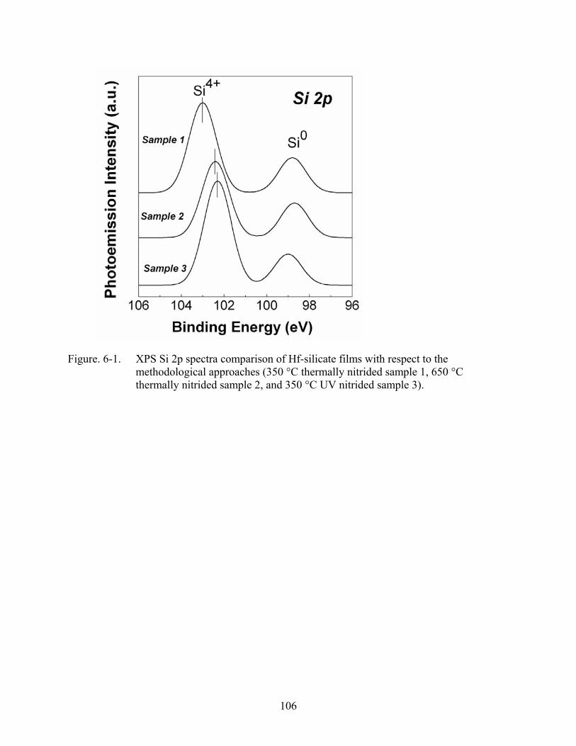
Figure. 6-1. XPS Si 2p spectra comparison of Hf-silicate films with respect to the methodological approaches (350 °C thermally nitrided sample 1, 650 °C thermally nitrided sample 2, and 350 °C UV nitrided sample 3).
106
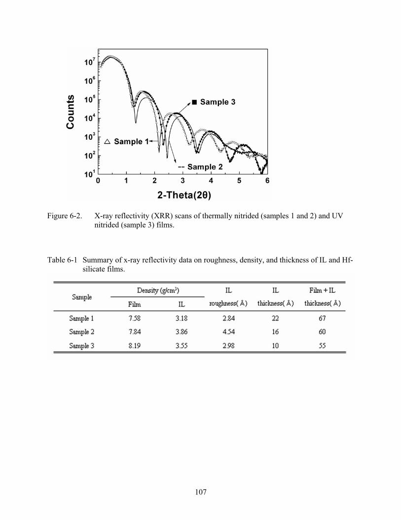
Figure 6-2. X-ray reflectivity (XRR) scans of thermally nitrided (samples 1 and 2) and UV nitrided (sample 3) films.
Table 6-1 Summary of x-ray reflectivity data on roughness, density, and thickness of IL and Hf-silicate films.
107
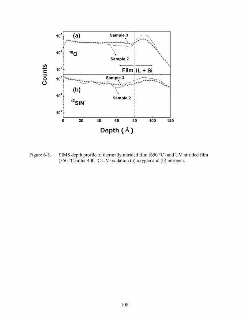
Figure 6-3. SIMS depth profile of thermally nitrided film (650 °C) and UV nitrided film (350 °C) after 400 °C UV oxidation (a) oxygen and (b) nitrogen.
108
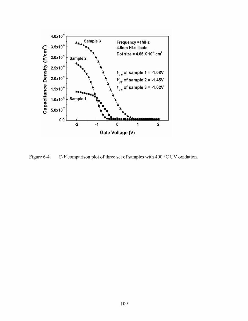
Figure 6-4. C-V comparison plot of three set of samples with 400 °C UV oxidation.
109
CHAPTER 7 UV ASSISTED LOW TEMPERATURE NITRIDATION & POST DEPOSITION OXIDATION
TECHNIQUE FOR HfO2 GATE DIELECTRIC
An evaluation of a low temperature method (~400 oC) for synthesis of nitrogen-
incorporated hafnia gate dielectric has been reported. This method is based on metal film growth
in ammonia ambient and subsequent oxidation under ultraviolet irradiation. X-ray
photoelectronic spectroscopy confirmed the presence of nitrided interface layer with a thickness
of ~12 Å. Equivalent oxide thickness values of around 11.5 Å and leakage current densities
lower than 1×10⁻⁴A/cm2 at an operation voltage (-1 V) were achieved. The post deposition UV
oxidation process was performed to check the interface oxidation resistance. The interface
growth rate showed that as the interface bonding characteristics changed from Si-N to Si-O
predominant bonding system of nitrogen incorporated films, the activation energy for oxygen
diffusion changed from 18.0 kJ/mol to 9.8 kJ/mole and the activation energy of un-doped hafnia
films was 2.3 kJ/mol in every growth region.
Introduction
Hafnium oxide has been receiving intense attention as a new gate dielectric material in
advanced metal oxide field effect transistors (MOSFETs) due to its reasonable permittivity (~
25), relatively large band gap (5.68 eV) and thermodynamic stability with Si.12,92,93 However, a
high temperature annealing of around 1000 oC, used in the conventional dopant activation
process, causes HfO2 film crystallization ( ~ 500 oC) and a low-k interface layer (IL) formation
between the film and substrate.30,39,94,95 To suppress crystallization and the IL formation, nitrogen
incorporation in the film has been studied by different researchers using various deposition
techniques. Previous studies reported that nitrogen incorporation into high-k gate dielectric help
to improve the thermal stability and forms a thinner interface layer.30,39,114,115 The most common
method for nitrogen incorporation is a deposition technique using carbon based gaseous
110
precursors such as Hf[N(CH3)2]4 and Hf[N(CH3)(C2H5)]4 followed by post deposition nitridation
(rapid thermal annealing, NH3 ambient) under high temperatures ( > 650 oC). In addition, due to
the large amount of oxygen related defects in the deposited films,116,129 high temperature ( > 700
oC) post deposition annealing (PDA) in oxidation/reduction ambient must be employed for defect
curing.116,129 As a result of high temperature nitridation and oxidation processes, unexpected
interface degradation was observed, which can potentially hinder scaling the device down in
size.116,117 As ultraviolet (UV) light irradiation has been reported to create highly reactive species
by photochemical dissociation process,48,118-120 UV assisted nitridation techniques could
potentially lower the incorporation process temperature. Therefore, in this work, low temperature
nitrogen doping during the metal film deposition and in-situ oxidation under UV illumination is
introduced in order to prevent degradation caused by high temperature post deposition nitridation
and oxidation processes. Based on the nitridation method, the enhanced IL qualities (composition,
electrical properties and thickness) are discussed. In addition, the nitrogen incorporation effects
on the UV assisted low temperature oxidation process (IL growth rate, compositional change and
diffusion activation energy) are investigated.
Experimental
Hafnium metal films were deposited on MEMC p-type (100) pre-cleaned (SC1, 1% HF
solution and DI water rinse) Si substrates having a resistivity of 9-18 Ωcm by pulsed laser
deposition (PLD) at a temperature of 350 oC. A 254 nm wavelength KrF excimer laser was used
to ablate a high purity hafnium target (>99.99%). To compare the nitrogen doping efficiency
under the low temperature condition, three sets of samples were prepared at the same process
temperature of 350 oC; sample 1 was deposited in NH3 ambient (1×10⁻² Torr) with UV irradiation,
sample 2 was deposited in NH3 ambient without UV irradiation and sample 3 was deposited in
111
high vacuum conditions (1×10⁻⁶ Torr). Next, in order to oxidize the metal film, all of the samples
then underwent an in-situ oxidation at 400 oC in high purity oxygen at 300 Torr for 30 min with
UV illumination from a low pressure Hg lamp array. To compare the IL growth rate of each
experimental sets, the PDA time period (30 to 120 min) and temperature (400 to 550 oC)were
varied. The film and IL thickness was cross-checked by x-ray reflectivity (XRR) and high
resolution transmission electron microscopy (HRTEM JEOL 2100). XRR (PANalytical X’pert
system) was also used to determine the IL density. The chemical bonding characteristics of the
films and IL were confirmed by x-ray photoelectron spectroscopy (XPS, Perkins Elmer 5100)
using Mg Kα radiation (1253.6 eV). All the peaks were calibrated with respect to C 1s at 284.6
eV. In order to investigate near the interface bonding state, 90o take off angle were applied. In
order to investigate the electrical characteristics of the deposited or annealed dielectric films, a
metal-oxide-semiconductor (MOS) capacitor with Pt gate electrode was fabricated using the
shadow mask technique. The electrical properties of the films were characterized by current
density-voltage and capacitance-voltage measurements using a Keithley instruments Win-82
system. The interface trap density Dit was calculated by the conductance method.130
Results and Discussion
UV Assisted Low Temperature Growth of Hafnia Film
Figure 7-1 shows the Si 2p scans for three sets of samples after 30 minutes of oxidation
processing. The Si4+ region of the peak in the UV assisted nitrided film (sample 1) undergoes a
shift of approximately 0.5 eV towards a lower binding energy in comparison to the thermally
nitrided film (sample 2) and the vacuum deposited film (sample 3), suggesting a change in the
bonding environment at the film–Si interface. Because 90o take off angle can detect the
interaction near the interface, it is believed that the Si peak position variations originated from
112
the interface bonding environmental changes. Previous analyses have reported that in the case of
stoichiometric SiO2 and Si3N4 films, the Si4+ peaks are located at higher energy regions (103.6eV
for oxide and 101.7 eV for nitride) than the Si0 peak (99.3eV in this experiment) which comes
from the Si substrate.121-124 Hence, the shift in peak of the UV assisted nitrided sample, away
from Si-N and towards Si-O bonding, is due to the interaction between Si-N atoms with oxygen
at film-Si interface. Since the magnitude of the shift is not very large, the influence of oxygen
involved in this interaction is assumed to be minimal. The nitrogen amount, analyzed using
appropriate sensitivity factors (not shown) of the UV assisted sample 1, was around 7 % which is
comparable to the high temperature process,[7] whereas for that of thermally nitrided sample 2
showed a lower content (~1 %). Since the nitridation efficiency is reduced at low temperatures,
other energy sources e.g. UV radiation which could assist the generation of reactive species
should be used, in order to incorporate nitrogen into the films at low temperatures ( below 350
oC). Cross-sectional HRTEM imaging was used to measure the interfacial layer thickness. Figure
7-2 shows the HRTEM micrographs of sample 1 and 3. The film thickness including the IL was
approximately same for the samples, whereas the IL thickness of the nitrogen incorporated
sample (1.2 nm) was thinner than that of the vacuum deposited sample (2.1 nm). It should be
noted that the reduced thickness of the IL in the UV assisted nitrided sample is comparable to the
values obtained by high temperature assisted techniques such as atomic layer deposition by with
rapid thermal annealing.114,115,125 In general, a reaction in the IL depends on the energetic species
of the deposition system because the conditions affect the mixing of atoms and chemical
reactions occurring near the substrate by influencing momentum transfer and diffusion.125,131
Therefore, the similar IL thickness with results of high temperature process indicate that the
oxidation efficiency of UV oxidation process is comparable with high temperature process. Also,
113
even though UV assisted oxidation has been shown to increase the growth of the IL due to the
presence of the highly active oxygen species,118,119 IL thickness of the UV nitrided sample 1
being less than that of non-nitrided vacuum deposited sample 3 can be understood by the Si-N
bonding predominant IL causing high resistance to oxidation.
Figure 7-3 (a) shows the C-V comparison plot for the three samples after 400 UV
oxidation. The UV assisted nitrided sample 1 showed a substantial increase in overall
capacitance in comparison with other samples. A maximum capacitance density of ~3.0 µF/cm2
corresponding to an EOT of 11.5 Å and a dielectric constant of approximately 21.7 were
determined for sample 1. The non-nitrided sample 3 exhibited the lowest capacitance of ~1.15
µF/cm2 corresponding to an EOT greater than 25 Å. The larger EOT in non-nitrided sample can
be attributed to the thick IL and to a low permittivity of undoped IL. The thermally nitrided
sample 2 showed a capacitance and EOT value similar to sample 3 due to the low nitridation
efficiency as described above. The estimated Dit values in the samples were 2×10¹², 8×10¹¹ and
3×10¹¹ eV-1cm-2 for UV assisted nitrided sample 1, thermally nitrided sample 2 and undoped
sample 3 respectively. The high interface trap density in the UV assisted nitrided sample is due
to the positively charged nitrogen incorporation and high efficiency of UV assisted nitridation
processes. The increase in trap density with nitrogen incorporation is consistent with the report
by Fedorenko et al.49 The leakage current density for nitrided and non-nitrided samples is shown
in Figure 3b. All the samples exhibited leakage current densities less than 10-4 A/cm2 at -1 V gate
bias. The low leakage density levels mean that the leakage current of the nitrided sample was not
seriously affected by the high interface trap density. From the fact that similar IL thickness
(figure 7-2) and Dit value of sample 3 with reported high temperature HfO2/Si film grown using
114
ALD and treated to a 1000 oC PDA process,49,132 it is believed that the oxidation efficiency of the
UV assisted low temperature process was comparable to the thermal oxidation process.
UV Assisted Oxidation Resistance of Hafnia Film
To study the effect of nitrogen on the PDA characteristics in UV assisted oxidizing
ambient conditions, post oxidation temperatures were varied from 400 oC to 550 oC. Figure 7-4
shows the IL thickness dependences of sample 1 and 3 on the oxidation time and temperature.
The IL thickness was cross-checked by HRTEM and x-ray reflectivity measurements (XRR).
The vacuum deposited samples showed relatively thicker interfacial layers and faster growth
rates than the nitried samples. The oxide growth rate in the vacuum deposited film was 2.5~2.8
Å /min, and the growth rate in the nitrogen incorporated films was 0.5~1 Å /min in the same
temperature range (400~550 oC). In the case of UV assisted nitrogen incorporated samples
oxygen diffusion to the Si substrate was hindered. This is due to the Si-N bonded interfacial
layer and the multiplicity of the NO oxidation state formation.109 It has been reported that
diffusion was more suppressed in the Si–O–N network in the N-incorporated hafnia film than in
the Si–O network in the hafnia film without N incorporation.133 Therefore, there was a drastic
increase in the IL thickness with oxidation time in non-nitrided samples due to the absence of the
Si-N bonded IL.
In order to investigate the IL density variation with respect to the oxidation process, the IL
densities of sample 1 and 3 from XRR analysis is shown in Figure 7-5. XRR has been reported to
be an effective method to characterize high-k materials since most high-k materials have a
density greater than Si and any interfacial reaction can be detected.134 The IL densities were 2.82
g/cm3 for the UV assisted nitrided film and 1.95 g/cm3 for non-nitrided film without post heat
treatment. Since the density of amorphous SiO2 and Si3N4 film are known to be ~ 2.2 and 3.1
g/cm3, respectively, the higher IL density of as deposited nitrided film as compared to non-
115
nitrided film can be attributed to nitrogen incorporation. As the UV assisted PDA time is
increased, the IL density of both samples exhibited similar values ~2.3 g/cm3 which are close to
the amorphous SiO2 film density. It should be noted that the film and IL experienced the
densification process during PDA as in the case of sample 3 where the film and interface density
increased with PDA time.105,106 However, in the case of UV assisted nitrided sample, the
interface density decreased with PDA process. The reduced interface density could be explained
by change in the bonding environment with interface oxidation.
In order to confirm the bonding environments of the IL after the UV assisted PDA process,
the Si 2p peak positions were analyzed by XPS. The Si 2p peak position is shown as a function
of oxidation time in Figure 7-6. The binding energy (BE) of the Si4+ nitrided sample which
underwent 30 minutes oxidation was found to be 102.5 eV, further increase in oxidation time to
90 and 120 minutes shifts the peak to 102.9 eV and 103.3 eV respectively(figure 6a). Since a
large amount of oxygen species are consumed by the metal film oxidation, oxygen diffusion to
the substrate can be assumed to be minimal during the 30 minutes oxidation time. Hence, the Si4+
peak location represented a predominantly Si-N bonding system. The 102.5 eV peak position of
30 min oxidized sample is very similar with the peak position of ALD grown HfSiON film,
indicating the Si-N predominant interface bonding characteristics.114,115,131 However, with
increasing oxidation time, the oxygen diffusion to Si increased leading to the formation of Si-O-
N bonding thus causing the peak position to shift to higher energies. Finally, for the 120 minutes
oxidation of sample 1, the Si4+ peak was spread and the peak position moved to high BE region
indicating the existence of various Si related bonding with a dominant Si-O bonding system. In
contrast, the non-nitrided samples did not exhibit peak shifts (103.5eV) with annealing periods,
as shown in figure 6b, implying that the interfacial bonding characteristic showed a predominant
116
Si-O bonding environment from the initial stage of the PDA process. The separation between Si0
and Si4+ peaks after 120 minutes of oxidation was about 4.1-4.3 eV which is similar to the
energy separation of SiO2 film grown by thermal oxidation.136 It also ascertains that predominant
Si-O bonding environment after 120 min oxidation.
Since the UV illumination process generates highly energetic oxygen species, the IL
oxidation process can be assumed to be an oxygen diffusion limited process and the oxygen
diffusivity would be affected by film composition and interface layer properties.116 Because
incorporated nitrogen has multiple state with oxygen, nitrogen incorporated hafnia film In order
to obtain the activation energy for oxygen diffusion with interface bonding characteristics under
UV oxidation ambient conditions, Arrhenius plots for interfacial growth with different time
ranges were plotted. Linear fits of the data were then used to obtain the activation energies(figure
7-7 (a)). Figure 7-7 (b) shows the comparison of activation energies of sample 1 and 3 with
respect to oxidation times. Region 1 refers to the oxidation time range between 30 and 60 min,
the activation energy of the UV assisted nitrogen-doped sample was 18 kJ/mol, whereas the
activation energy of vacuum deposited sample was 2.3 kJ/mol. The UV assisted nitrided samples
had a higher activation energy because of the Si-O-N bonding character of IL and the tendency
of nitrided hafnia to trap oxygen.117 Region 2 refers to the oxidation period between 90 and 120
min, since the IL characteristics changed to the predominantly lower density Si-O bonding phase,
the activation energy of nitrogen doped sample was decreased to 9.8 kJ/mol. However, due to the
consistent bonding characteristics of the IL, the activation energy of the non-nitrided samples did
not vary with oxidation time.
Conclusions
The UV assisted low temperature metal oxidation technique for nitrogen doped hafnia gate
dielectric films was investigated. At low temperatures, thermal nitridation was not an effective
117
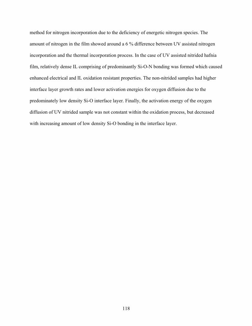
method for nitrogen incorporation due to the deficiency of energetic nitrogen species. The
amount of nitrogen in the film showed around a 6 % difference between UV assisted nitrogen
incorporation and the thermal incorporation process. In the case of UV assisted nitrided hafnia
film, relatively dense IL comprising of predominantly Si-O-N bonding was formed which caused
enhanced electrical and IL oxidation resistant properties. The non-nitrided samples had higher
interface layer growth rates and lower activation energies for oxygen diffusion due to the
predominately low density Si-O interface layer. Finally, the activation energy of the oxygen
diffusion of UV nitrided sample was not constant within the oxidation process, but decreased
with increasing amount of low density Si-O bonding in the interface layer.
118
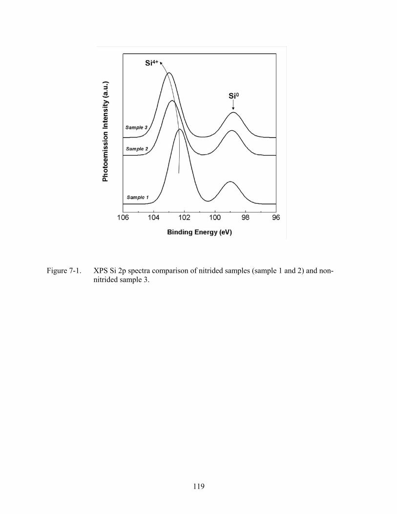
Figure 7-1. XPS Si 2p spectra comparison of nitrided samples (sample 1 and 2) and non-nitrided sample 3.
119
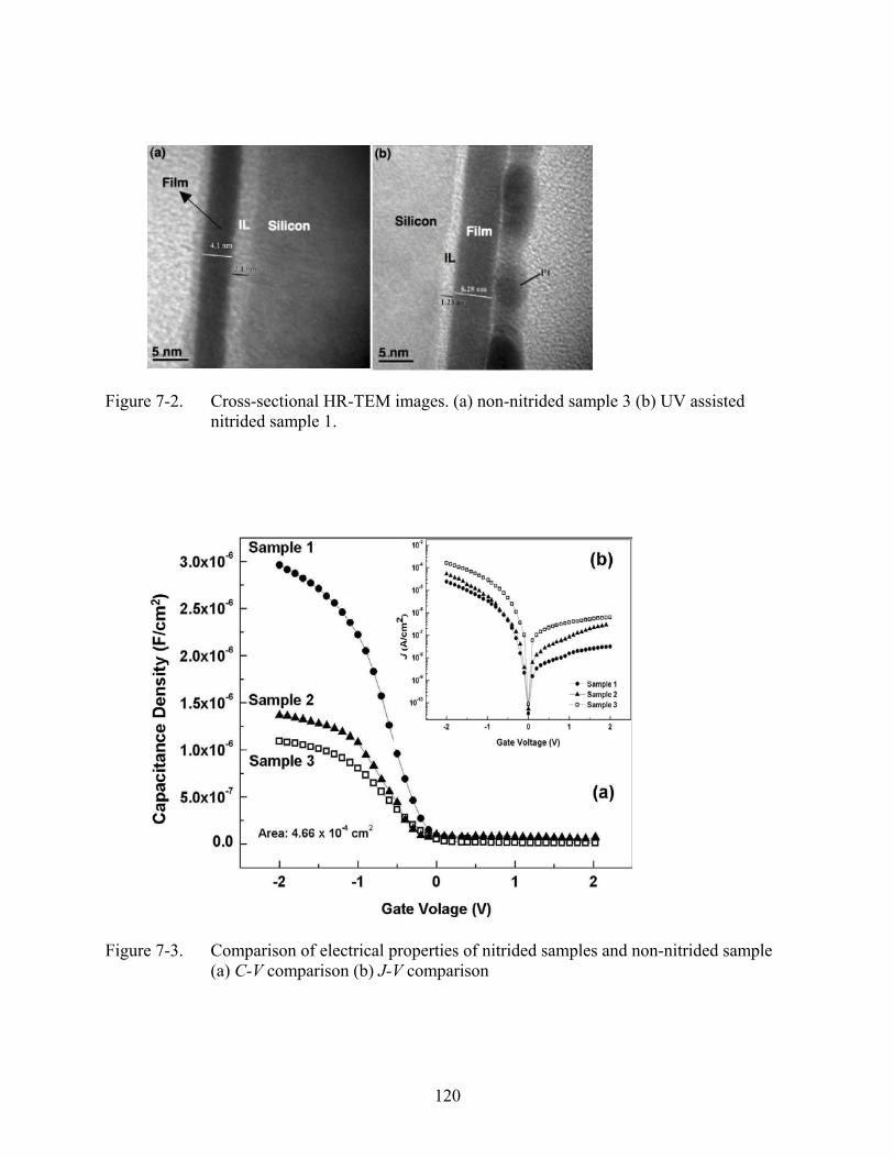
Figure 7-2. Cross-sectional HR-TEM images. (a) non-nitrided sample 3 (b) UV assisted nitrided sample 1.
Figure 7-3. Comparison of electrical properties of nitrided samples and non-nitrided sample (a) C-V comparison (b) J-V comparison
120
Figure 7-4. The interfacial layer thickness changes with respect to the PDA times for sample 1 and 3.
121
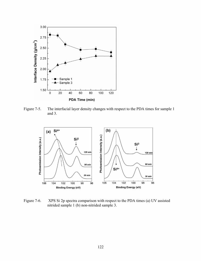
Figure 7-5. The interfacial layer density changes with respect to the PDA times for sample 1 and 3.
Figure 7-6. XPS Si 2p spectra comparison with respect to the PDA times (a) UV assisted nitrided sample 1 (b) non-nitrided sample 3.
122
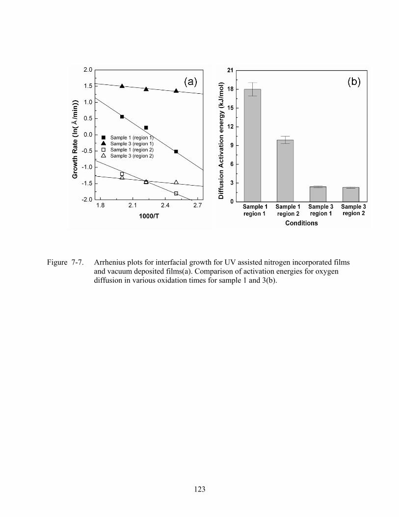
Figure 7-7. Arrhenius plots for interfacial growth for UV assisted nitrogen incorporated films and vacuum deposited films(a). Comparison of activation energies for oxygen diffusion in various oxidation times for sample 1 and 3(b).
123
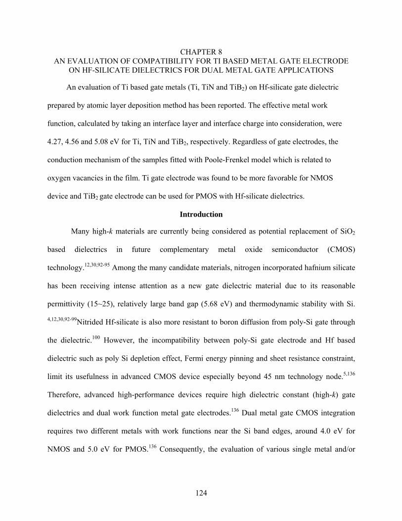
CHAPTER 8 AN EVALUATION OF COMPATIBILITY FOR TI BASED METAL GATE ELECTRODE
ON HF-SILICATE DIELECTRICS FOR DUAL METAL GATE APPLICATIONS
An evaluation of Ti based gate metals (Ti, TiN and TiB2) on Hf-silicate gate dielectric
prepared by atomic layer deposition method has been reported. The effective metal work
function, calculated by taking an interface layer and interface charge into consideration, were
4.27, 4.56 and 5.08 eV for Ti, TiN and TiB2, respectively. Regardless of gate electrodes, the
conduction mechanism of the samples fitted with Poole-Frenkel model which is related to
oxygen vacancies in the film. Ti gate electrode was found to be more favorable for NMOS
device and TiB2 gate electrode can be used for PMOS with Hf-silicate dielectrics.
Introduction
Many high-k materials are currently being considered as potential replacement of SiO2
based dielectrics in future complementary metal oxide semiconductor (CMOS)
technology.12,30,92-95 Among the many candidate materials, nitrogen incorporated hafnium silicate
has been receiving intense attention as a new gate dielectric material due to its reasonable
permittivity (15~25), relatively large band gap (5.68 eV) and thermodynamic stability with Si.
4,12,30,92-99Nitrided Hf-silicate is also more resistant to boron diffusion from poly-Si gate through
the dielectric.100 However, the incompatibility between poly-Si gate electrode and Hf based
dielectric such as poly Si depletion effect, Fermi energy pinning and sheet resistance constraint,
limit its usefulness in advanced CMOS device especially beyond 45 nm technology node.5,136
Therefore, advanced high-performance devices require high dielectric constant (high-k) gate
dielectrics and dual work function metal gate electrodes.136 Dual metal gate CMOS integration
requires two different metals with work functions near the Si band edges, around 4.0 eV for
NMOS and 5.0 eV for PMOS.136 Consequently, the evaluation of various single metal and/or
124
metal alloys on nitrogen incorporated Hf-silicate dielectric could be highlight for future
advanced CMOS technology development.
Because of good thermal stability and minimal interaction with high-k films, titanium
based materials could be an attractive candidate for metal gate application.137,138 Ti based
refractory materials such as TiN and TiB2 have been previously considered as a diffusion barrier
in metal contact formation due to its high electrical conductivity and excellent chemical inertness
at high temperature.139 In this chapter, the electrical characteristics of MOS devices with Ti
based metal gate (Ti, TiN and TiB2) on nitrogen incorporated Hf-silicate dielectric are
investigated. The effective metal work functions are extracted in order to examine its
compatibility with NMOS or PMOS devices. In addition, the conduction mechanism of Ti based
metal/Hf-silicate dielectric/ p-type Si MOS device is investigated.
Experimental Detail
HfSiOx films were deposited directly on MEMC p-type (100) pre-cleaned (SC1, 1% HF
solution and DI water rinse) 8 inch Si substrates with a resistivity of 3-25 Ωcm, by atomic layer
deposition (ALD) using GENUS Lynx2TM tool at 300oC. SiH[N(CH3)2]3 was used as Si
precursor where as Hf(NEtMe)4 (TEMAH) was employed as Hf precursor.19 The oxidizing
agents for TEMAH and Si were O3 and H2O, respectively. HfSiOx film deposition was followed
with nitrogen incorporation by rapid thermal anneal at 650 oC in NH3 ambience for 60 s. MOS
capacitors with Ti, TiN and TiB2 gate electrode were fabricated using RF magnetron sputtering.
All of the metal/compounds were deposited by Ar plasma assisted rf sputtering at a pressure of
15 mTorr and 150W rf (13.56 MHz) power. For all MOS devices, post metallization annealing
(PMA) was carried out in tube furnace at 400oC in forming gas (10% H2 / 90% N2) ambience for
30 min. The C-V characteristics were analyzed at high frequency 1 MHz using an HP 4294A
LCR meter and NCSU program was used to analyze the electrical measurements and extract the
125
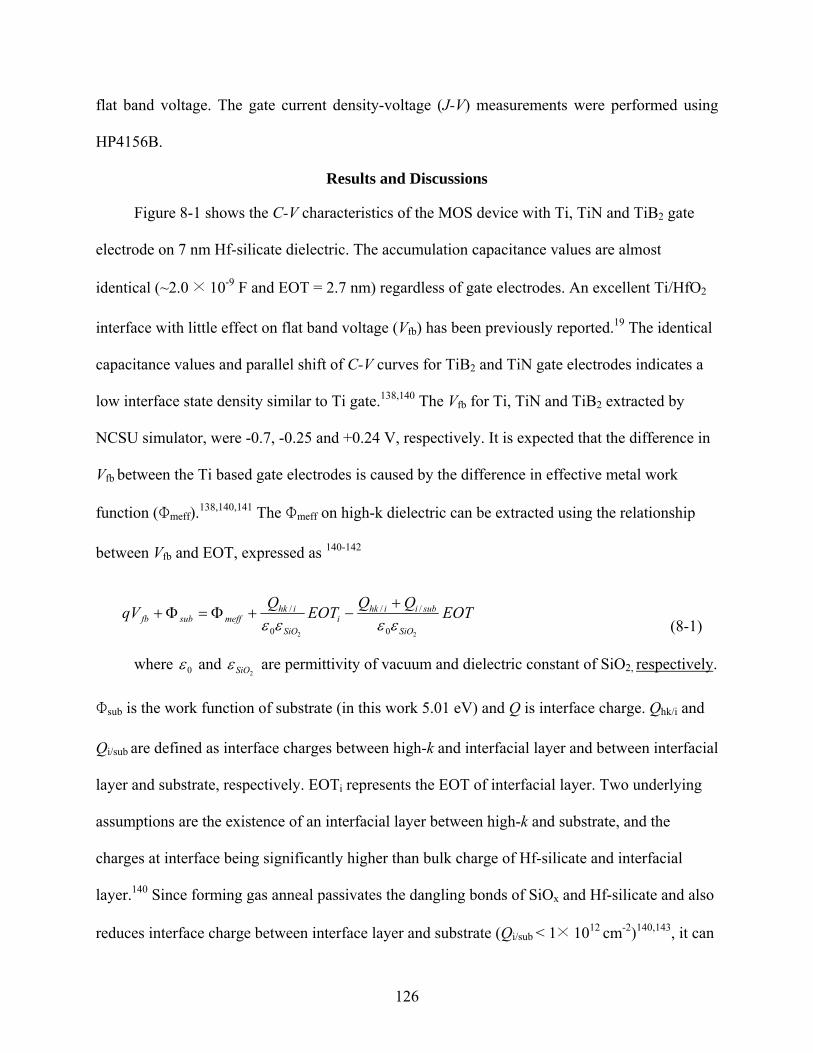
flat band voltage. The gate current density-voltage (J-V) measurements were performed using
HP4156B.
Results and Discussions
Figure 8-1 shows the C-V characteristics of the MOS device with Ti, TiN and TiB2 gate
electrode on 7 nm Hf-silicate dielectric. The accumulation capacitance values are almost
identical (~2.0 × 10⁻⁹ F and EOT = 2.7 nm) regardless of gate electrodes. An excellent Ti/HfO2
interface with little effect on flat band voltage (Vfb) has been previously reported.19 The identical
capacitance values and parallel shift of C-V curves for TiB2 and TiN gate electrodes indicates a
low interface state density similar to Ti gate.138,140 The Vfb for Ti, TiN and TiB2 extracted by
NCSU simulator, were -0.7, -0.25 and +0.24 V, respectively. It is expected that the difference in
Vfb between the Ti based gate electrodes is caused by the difference in effective metal work
function (Φmeff).138,140,141 The Φmeff on high-k dielectric can be extracted using the relationship
between Vfb and EOT, expressed as 140-142
(8-1) EOTQQEOTQqV
SiOi
Off
22 00 εεεεsubiihk
Si
ihkmesubfb
/// +−+Φ=Φ+
0ε and where 2SiOε are permittivity of vacuum and dielectric constant of SiO2, respectively.
Φsub is the work function of substrate (in this work 5.01 eV) and Q is interface charge. Qhk/i and
Qi/sub are defined as interface charges between high-k and interfacial layer and between interfacial
layer and substrate, respectively. EOTi represents the EOT of interfacial layer. Two underlying
assumptions are the existence of an interfacial layer between high-k and substrate, and the
charges at interface being significantly higher than bulk charge of Hf-silicate and interfacial
layer.140 Since forming gas anneal passivates the dangling bonds of SiOx and Hf-silicate and also
reduces interface charge between interface layer and substrate (Qi/sub < 1× 1012 cm-2)140,143, it can
126
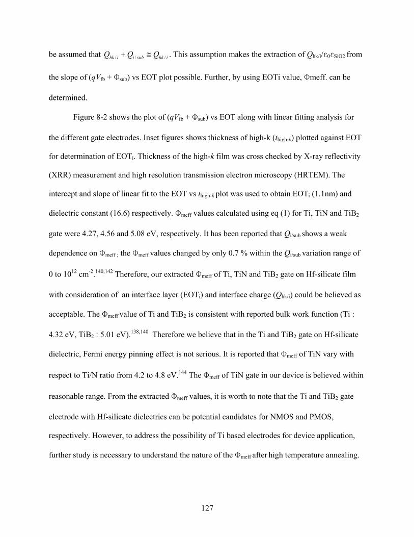
be assumed that . This assumption makes the extraction of Qhk/i/ε0εSiO2 from
the slope of (qVfb + Φsub) vs EOT plot possible. Further, by using EOTi value, Φmeff. can be
determined.
ihksubiihk QQQ /// ≅+
Figure 8-2 shows the plot of (qVfb + Φsub) vs EOT along with linear fitting analysis for
the different gate electrodes. Inset figures shows thickness of high-k (thigh-k) plotted against EOT
for determination of EOTi. Thickness of the high-k film was cross checked by X-ray reflectivity
(XRR) measurement and high resolution transmission electron microscopy (HRTEM). The
intercept and slope of linear fit to the EOT vs thigh-k plot was used to obtain EOTi (1.1nm) and
dielectric constant (16.6) respectively. Φmeff values calculated using eq (1) for Ti, TiN and TiB2
gate were 4.27, 4.56 and 5.08 eV, respectively. It has been reported that Qi/sub shows a weak
dependence on Φmeff ; the Φmeff values changed by only 0.7 % within the Qi/sub variation range of
0 to 1012 cm-2.140,142 Therefore, our extracted Φmeff of Ti, TiN and TiB2 gate on Hf-silicate film
with consideration of an interface layer (EOTi) and interface charge (Qhk/i) could be believed as
acceptable. The Φmeff value of Ti and TiB2 is consistent with reported bulk work function (Ti :
4.32 eV, TiB2 : 5.01 eV).138,140 Therefore we believe that in the Ti and TiB2 gate on Hf-silicate
dielectric, Fermi energy pinning effect is not serious. It is reported that Φmeff of TiN vary with
respect to Ti/N ratio from 4.2 to 4.8 eV.144 The Φmeff of TiN gate in our device is believed within
reasonable range. From the extracted Φmeff values, it is worth to note that the Ti and TiB2 gate
electrode with Hf-silicate dielectrics can be potential candidates for NMOS and PMOS,
respectively. However, to address the possibility of Ti based electrodes for device application,
further study is necessary to understand the nature of the Φmeff after high temperature annealing.
127
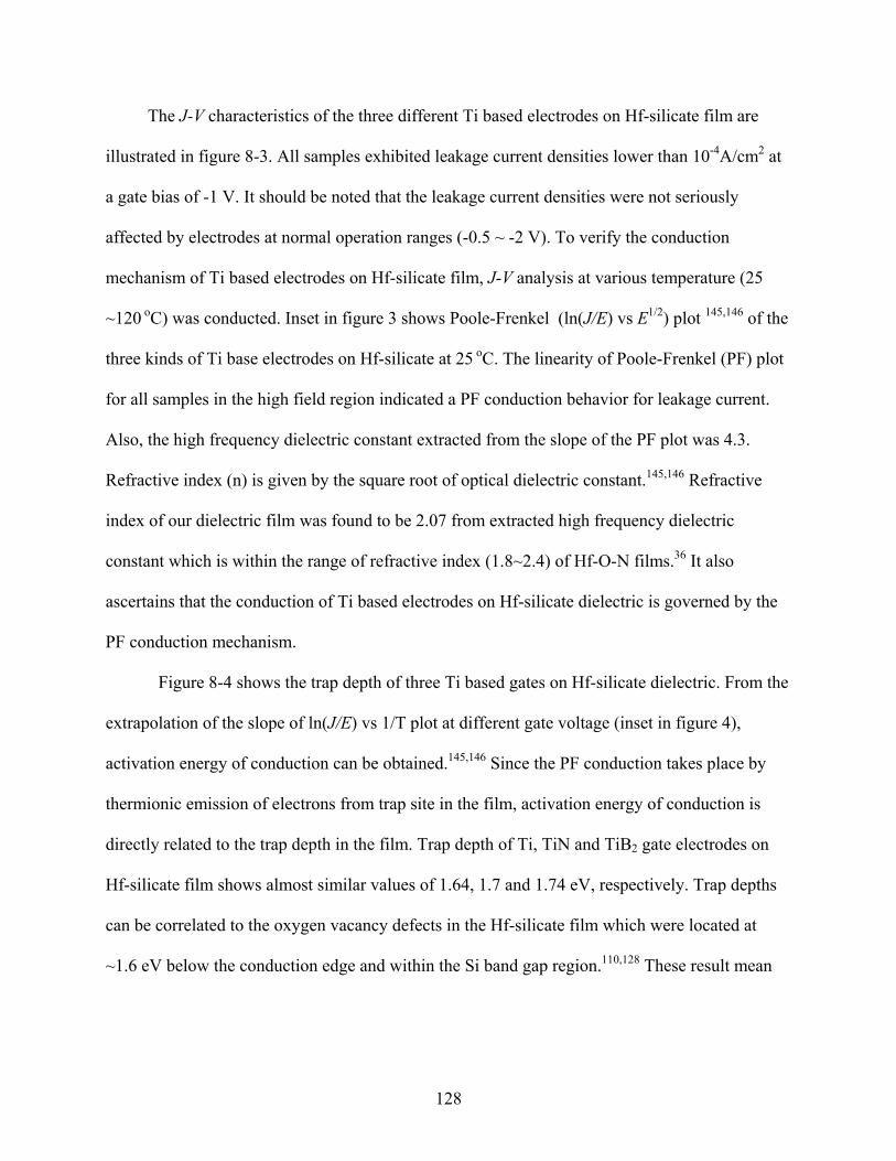
The J-V characteristics of the three different Ti based electrodes on Hf-silicate film are
illustrated in figure 8-3. All samples exhibited leakage current densities lower than 10-4A/cm2 at
a gate bias of -1 V. It should be noted that the leakage current densities were not seriously
affected by electrodes at normal operation ranges (-0.5 ~ -2 V). To verify the conduction
mechanism of Ti based electrodes on Hf-silicate film, J-V analysis at various temperature (25
~120 oC) was conducted. Inset in figure 3 shows Poole-Frenkel (ln(J/E) vs E1/2) plot 145,146 of the
three kinds of Ti base electrodes on Hf-silicate at 25 oC. The linearity of Poole-Frenkel (PF) plot
for all samples in the high field region indicated a PF conduction behavior for leakage current.
Also, the high frequency dielectric constant extracted from the slope of the PF plot was 4.3.
Refractive index (n) is given by the square root of optical dielectric constant.145,146 Refractive
index of our dielectric film was found to be 2.07 from extracted high frequency dielectric
constant which is within the range of refractive index (1.8~2.4) of Hf-O-N films.36 It also
ascertains that the conduction of Ti based electrodes on Hf-silicate dielectric is governed by the
PF conduction mechanism.
Figure 8-4 shows the trap depth of three Ti based gates on Hf-silicate dielectric. From the
extrapolation of the slope of ln(J/E) vs 1/T plot at different gate voltage (inset in figure 4),
activation energy of conduction can be obtained.145,146 Since the PF conduction takes place by
thermionic emission of electrons from trap site in the film, activation energy of conduction is
directly related to the trap depth in the film. Trap depth of Ti, TiN and TiB2 gate electrodes on
Hf-silicate film shows almost similar values of 1.64, 1.7 and 1.74 eV, respectively. Trap depths
can be correlated to the oxygen vacancy defects in the Hf-silicate film which were located at
~1.6 eV below the conduction edge and within the Si band gap region.110,128 These result mean
128
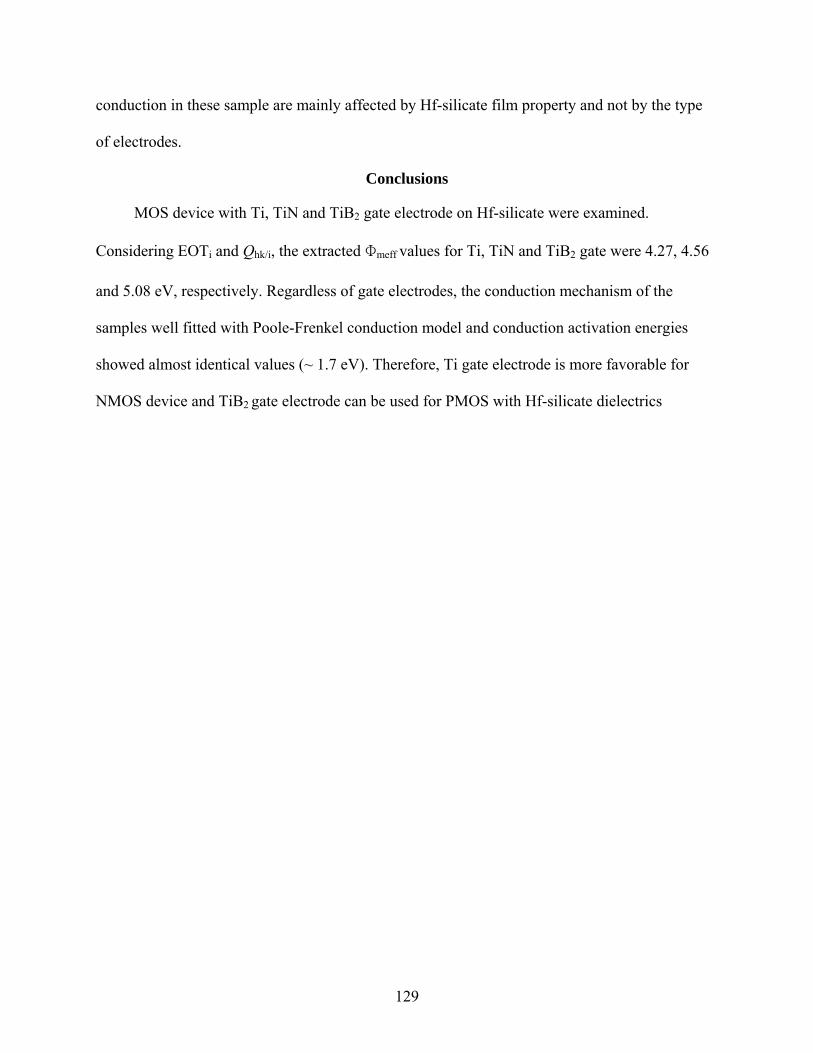
conduction in these sample are mainly affected by Hf-silicate film property and not by the type
of electrodes.
Conclusions
MOS device with Ti, TiN and TiB2 gate electrode on Hf-silicate were examined.
Considering EOTi and Qhk/i, the extracted Φmeff values for Ti, TiN and TiB2 gate were 4.27, 4.56
and 5.08 eV, respectively. Regardless of gate electrodes, the conduction mechanism of the
samples well fitted with Poole-Frenkel conduction model and conduction activation energies
showed almost identical values (~ 1.7 eV). Therefore, Ti gate electrode is more favorable for
NMOS device and TiB2 gate electrode can be used for PMOS with Hf-silicate dielectrics
129
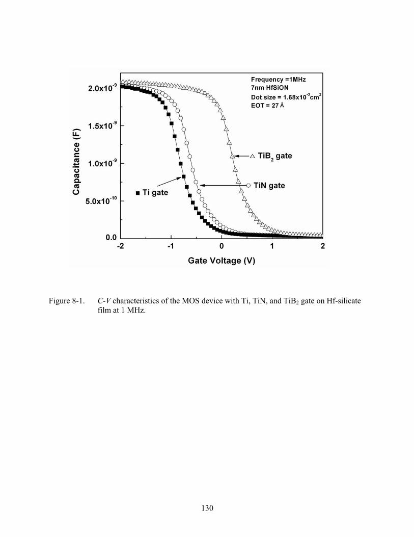
Figure 8-1. C-V characteristics of the MOS device with Ti, TiN, and TiB2 gate on Hf-silicate film at 1 MHz.
130
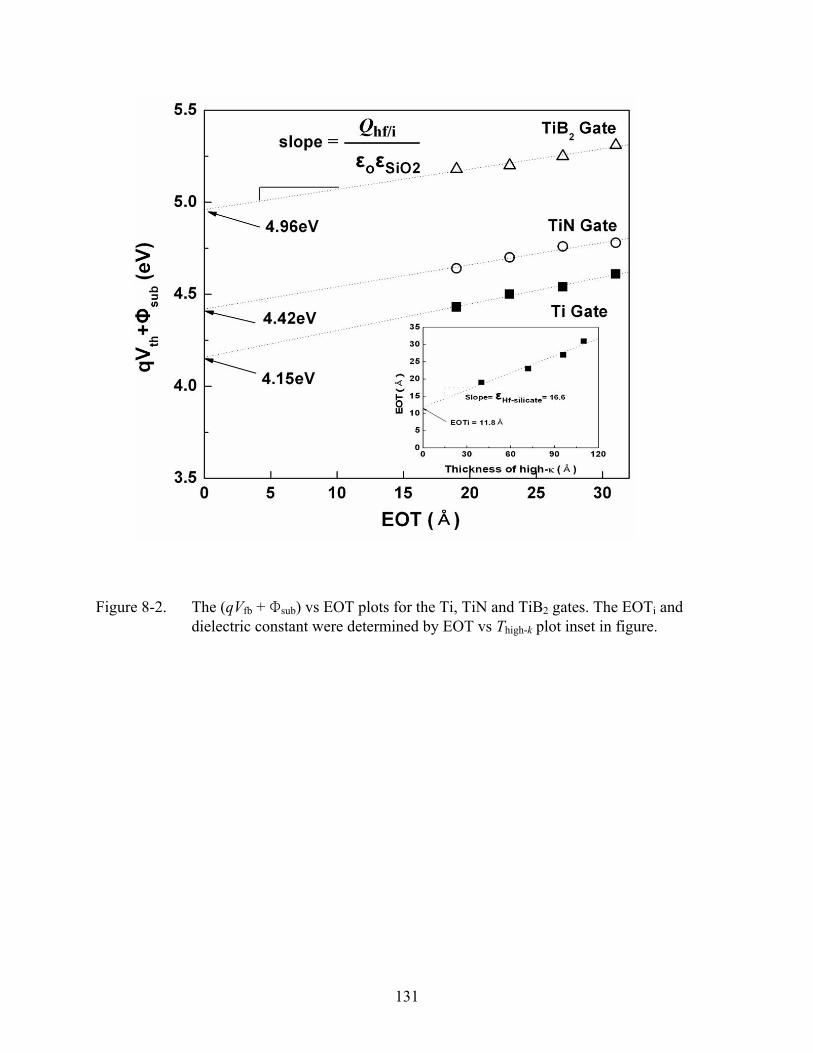
Figure 8-2. The (qVfb + Φsub) vs EOT plots for the Ti, TiN and TiB2 gates. The EOTi and dielectric constant were determined by EOT vs Thigh-k plot inset in figure.
131
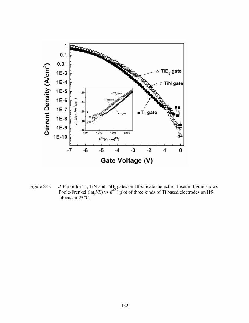
Figure 8-3. J-V plot for Ti, TiN and TiB2 gates on Hf-silicate dielectric. Inset in figure shows Poole-Frenkel (ln(J/E) vs E1/2) plot of three kinds of Ti based electrodes on Hf-silicate at 25 oC.
132
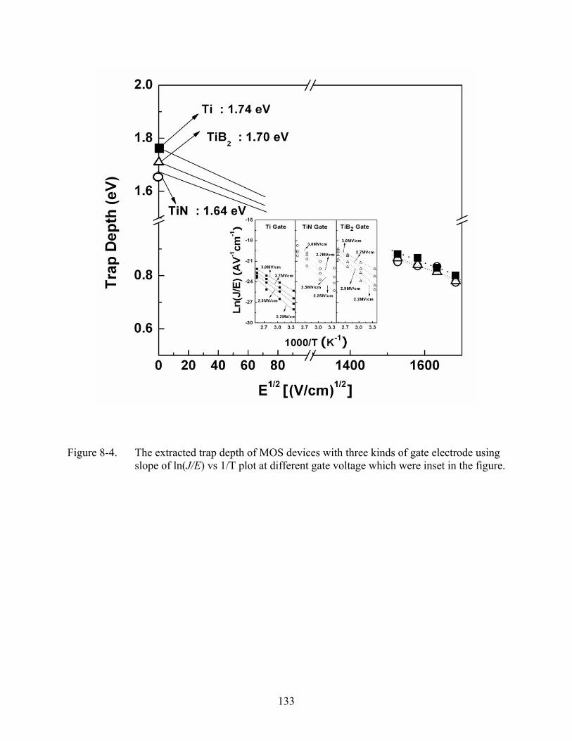
Figure 8-4. The extracted trap depth of MOS devices with three kinds of gate electrode using slope of ln(J/E) vs 1/T plot at different gate voltage which were inset in the figure.
133
CHAPTER 9 AN EVALUATION OF THERMAL STABILITY OF TIB2 METAL GATE ON HF-SILICATE
FOR P-CHANNEL METAL OXIDE SEMICONDUCTOR APPLICATION
An evaluation of TiB2 gate metal on Hf-silicate dielectric prepared by atomic layer
deposition method has been reported. The extracted effective metal work function for TiB2 gate
was about 5.08 eV. The work function showed almost identical values and sharp interface
between metal and dielectric was confirmed after post deposition annealing by 1000 oC. The
work function lowering (4.91 eV) at 1100 oC was caused by metal-dielectric intermixing and
oxygen vacancy formation. TiB2 gate electrode was found to be suitable for use in p-channel
metal oxide semiconductor device.
Introduction
Nitrogen incorporated hafnium silicate has been receiving intense attention as a gate
dielectric material for complementary metal oxide semiconductor (CMOS) devices.4,12,92-100
However, the incompatibility between poly-Si gate electrode and Hf based dielectric such as
poly Si depletion effect, Fermi energy pinning and sheet resistance constraint, limit its usefulness
in advanced CMOS device especially beyond 45 nm technology node.5,76 Therefore, advanced
high-performance devices require high dielectric constant (high-k) gate dielectrics and metal gate
electrodes. Since p-type MOS integration requires metal with work function near the Si band
edge, close to 5.0 eV, PMOS metal candidates are limited. Potential candidates such as Ru, RuO2,
and Mo have been studied for PMOS application. However, Ru electrode on SiO2 film showed
complete intermixing at high temperature (>950 oC). Physical and electrical instability of Mo and
RuO2 gate on high-k material after high temperature annealing (>850 oC) has also been reported.
Consequently, the evaluation of various single metal or metal alloys on nitrogen incorporated Hf-
silicate dielectrics after high temperature post deposition annealing (PDA) process could be
highlight for future advanced CMOS technology development.
134
Because of thermal stability and chemical inertness, titanium based refractory materials
could be an attractive candidate for metal gate application.137-139 In the Chapter 8, the possibility
of TiB2 gate electrode as a PMOS application has been proposed.147 However, to address the
possibility of TiB2 electrode for device application, the thermal stability of TiB2 electrode on Hf-
silicate and nature of metal work function after high temperature annealing should be
investigated. Therefore, in this chapter, the electrical characteristics of MOS devices with TiB2
metal gate on nitrogen incorporated Hf-silicate dielectric for PMOS application are investigated.
In addition, the stability of electrical and physical properties with respect to the post deposition
annealing (PDA) temperature is examined.
Experimental Detail
HfSiOx films were deposited directly on p-type (100) pre-cleaned (SC1, 1% HF solution
and DI water rinse) 8 inch Si substrates with a resistivity of 3-25 Ωcm, by atomic layer
deposition (ALD) using GENUS Lynx2TM at 300oC. SiH[N(CH3)2]3 was used as Si precursor
where as Hf(NEtMe)4 (TEMAH) was employed as Hf precursor. The oxidizing agents for
TEMAH and Si were O3 and H2O, respectively. HfSiOx film deposition was followed with
nitrogen incorporation by rapid thermal anneal at 650 oC in NH3 ambience for 60 s. MOS
capacitors with TiB2 gate electrode were fabricated using RF magnetron sputtering. Sintered
TiB2 ceramic target was used for TiB2 metal deposition. To minimize the external resistance, a
metallization scheme of Au(50nm)/Ti(10nm) was used on TiB2 films. All of metals and metal
alloy were deposited by Ar plasma assisted rf sputtering at a pressure of 15 mTorr and 150W rf
(13.56 MHz) power. To verify the thermal stability, post deposition annealing (PDA)
temperature was varied from 600 to 1100 oC in N2 ambience with 30 sec duration time. For all
MOS devices, post metallization annealing (PMA) was carried out in tube furnace at 400oC in
forming gas (10% H2 / 90% N2) ambience for 30 min. Auger electron spectroscopy (AES) depth
135
profile analysis was conducted using a Physical Electronics 660 Scanning Auger Microprobe.
The electron beam conditions were 10 keV, 1 mA beam current at 45o from sample normal. The
C-V characteristics were analyzed at high frequency 1 MHz using an HP 4294A LCR meter and
North Carolina State University (NCSU) program was used to analyze the electrical
measurements and extract the flat band voltage (Vfb). The gate current density-voltage (J-V)
measurements were performed using HP4156B. The effective metal work function (Φmeff) was
extracted using Vfb - EOT method.140-142 The interface state densities (Dit) were extracted by the
method of Lehovec.105,106
Results and Discussion
Figure 9-1 (a) shows the C-V characteristics of the MOS device with TiB2 gate electrode
on 7 nm Hf-silicate dielectric after different PDA treatments temperatures. The accumulation
capacitance and flat band voltage (Vfb) are almost identical (~2.0 × 10⁻⁹ F, EOT = 2.7 nm and Vfb
= 0.24 V) for samples annealed up to 1000 oC, whereas, the C-V curve of sample annealed at
1100 oC showed lower capacitance than others and displayed large parallel shift to negative bias
region (C ~ 1.2 × 10⁻⁹ F and Vfb = 0.13 V). An excellent TiB2/Hf-Silicate interface of as-
deposited sample with little effect on flat band voltage (Vfb) has been reported in our previous
work.19,20 The identical capacitance for TiB2 gate electrodes after different PDA treatment
indicates minimal reaction between electrode and dielectric.138,140,147 The stretched curve of
1100oC annealed sample indicates the increase in interface state density (Dit). The interface state
densities at flat band voltage showed almost similar value (~5.5 × 10¹¹ eV-1cm-2) up to 1000oC
annealed device. Whereas the increase in Dit (~11.3 × 10¹¹ eV-1cm-2) of 1100oC annealed sample
was measured. This lower capacitance and higher Dit at 1100oC annealed sample are attributed to
interlayer growth which we can confirm in Fig. 3. The variations of (qVfb + Φsub) with respect to
136
the EOT after high temperature annealing is presented in figure 1b (Φsub is the work function of
substrate in this work 5.01 eV). The Vfb for TiB2 metal gate did not change up to 1000 oC anneal.
However, for 1100 oC annealed TiB2 metal gate, a major shift of Vfb and an increase in slope of
(qVfb + Φsub) vs EOT plot compared with other samples indicated change of metal work function
and increase in fixed charge at IL. From the (qVfb + Φsub) vs EOT plot and EOT vs thickness of
high-k plot (not shown), we can extract effective metal work function (Φmeff) with consideration
of IL and fixed charge. These values are presented in inset of figure 9-1 (b). Φmeff of as deposited,
700, 900 and 1000 oC annealed TiB2 gate metal showed almost identical values (~5.07 eV).
However, a lower value of Φmeff (~4.91 eV) for 1100 oC annealed TiB2 gate metal was found. A
possible reason for decrease in work function after 1100 oC anneal could be instability of TiB2
alloy after 1100 oC exposure. Hence, it can be expected that degradation of capacitance values
and Φmeff was caused by intermixing of metal gate and dielectric at 1100 oC annealing.
In order to check the intermixing of metal and Hf-silicate, AES analysis was conducted.
The AES depth profiles from the as deposited, 900 and 1100 oC annealed samples are shown in
figure 9-2. The as-deposited sample shows sharp interfaces between the metal and Hf-silicate.
Till 900 oC annealing, there is no significant movement of Ti or B through the underlying layers
and metal/dielectric maintained sharp interface as in the case of as-deposited sample even if part
of Ti diffused out to the surface. TiB2 appears to be a barrier for Ti diffusion, which probably
excludes formation of TiN and TiSi phases at the interface of the Hf-silicate.139 However, after
1100 oC annealing, metal and dielectric film intermixed and there is an accompanying decrease
in abruptness of the TiB2 interface with the Hf-silicate film. The lowering of Φmeff (4.91 eV) can
137
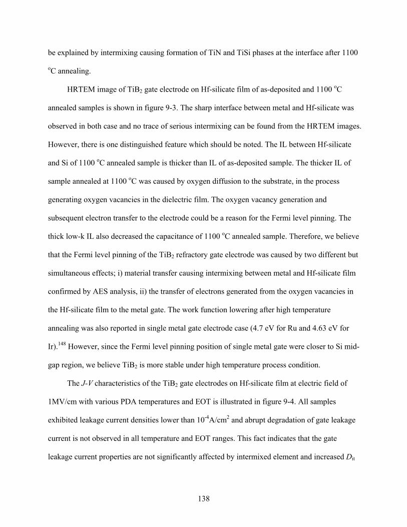
be explained by intermixing causing formation of TiN and TiSi phases at the interface after 1100
oC annealing.
HRTEM image of TiB2 gate electrode on Hf-silicate film of as-deposited and 1100 oC
annealed samples is shown in figure 9-3. The sharp interface between metal and Hf-silicate was
observed in both case and no trace of serious intermixing can be found from the HRTEM images.
However, there is one distinguished feature which should be noted. The IL between Hf-silicate
and Si of 1100 oC annealed sample is thicker than IL of as-deposited sample. The thicker IL of
sample annealed at 1100 oC was caused by oxygen diffusion to the substrate, in the process
generating oxygen vacancies in the dielectric film. The oxygen vacancy generation and
subsequent electron transfer to the electrode could be a reason for the Fermi level pinning. The
thick low-k IL also decreased the capacitance of 1100 oC annealed sample. Therefore, we believe
that the Fermi level pinning of the TiB2 refractory gate electrode was caused by two different but
simultaneous effects; i) material transfer causing intermixing between metal and Hf-silicate film
confirmed by AES analysis, ii) the transfer of electrons generated from the oxygen vacancies in
the Hf-silicate film to the metal gate. The work function lowering after high temperature
annealing was also reported in single metal gate electrode case (4.7 eV for Ru and 4.63 eV for
Ir).148 However, since the Fermi level pinning position of single metal gate were closer to Si mid-
gap region, we believe TiB2 is more stable under high temperature process condition.
The J-V characteristics of the TiB2 gate electrodes on Hf-silicate film at electric field of
1MV/cm with various PDA temperatures and EOT is illustrated in figure 9-4. All samples
exhibited leakage current densities lower than 10-4A/cm2 and abrupt degradation of gate leakage
current is not observed in all temperature and EOT ranges. This fact indicates that the gate
leakage current properties are not significantly affected by intermixed element and increased Dit
138
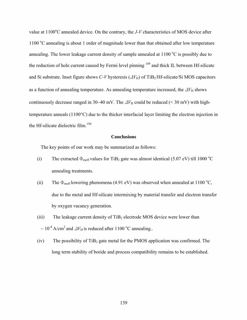
value at 1100oC annealed device. On the contrary, the J-V characteristics of MOS device after
1100 oC annealing is about 1 order of magnitude lower than that obtained after low temperature
annealing. The lower leakage current density of sample annealed at 1100 oC is possibly due to
the reduction of hole current caused by Fermi level pinning 149 and thick IL between Hf-silicate
and Si substrate. Inset figure shows C-V hysteresis (ΔVH) of TiB2/Hf-silicate/Si MOS capacitors
as a function of annealing temperature. As annealing temperature increased, the ΔVH shows
continuously decrease ranged in 30~40 mV. The ΔVH could be reduced (< 30 mV) with high-
temperature anneals (1100°C) due to the thicker interfacial layer limiting the electron injection in
the Hf-silicate dielectric film.150
Conclusions
The key points of our work may be summarized as follows:
(i) The extracted Φmeff values for TiB2 gate was almost identical (5.07 eV) till 1000 oC
annealing treatments.
(ii) The Φmeff lowering phenomena (4.91 eV) was observed when annealed at 1100 oC,
due to the metal and Hf-silicate intermixing by material transfer and electron transfer
by oxygen vacancy generation.
(iii) The leakage current density of TiB2 electrode MOS device were lower than
~ 10-4 A/cm2 and ΔVH is reduced after 1100 oC annealing..
(iv) The possibility of TiB2 gate metal for the PMOS application was confirmed. The
long term stability of boride and process compatibility remains to be established.
139
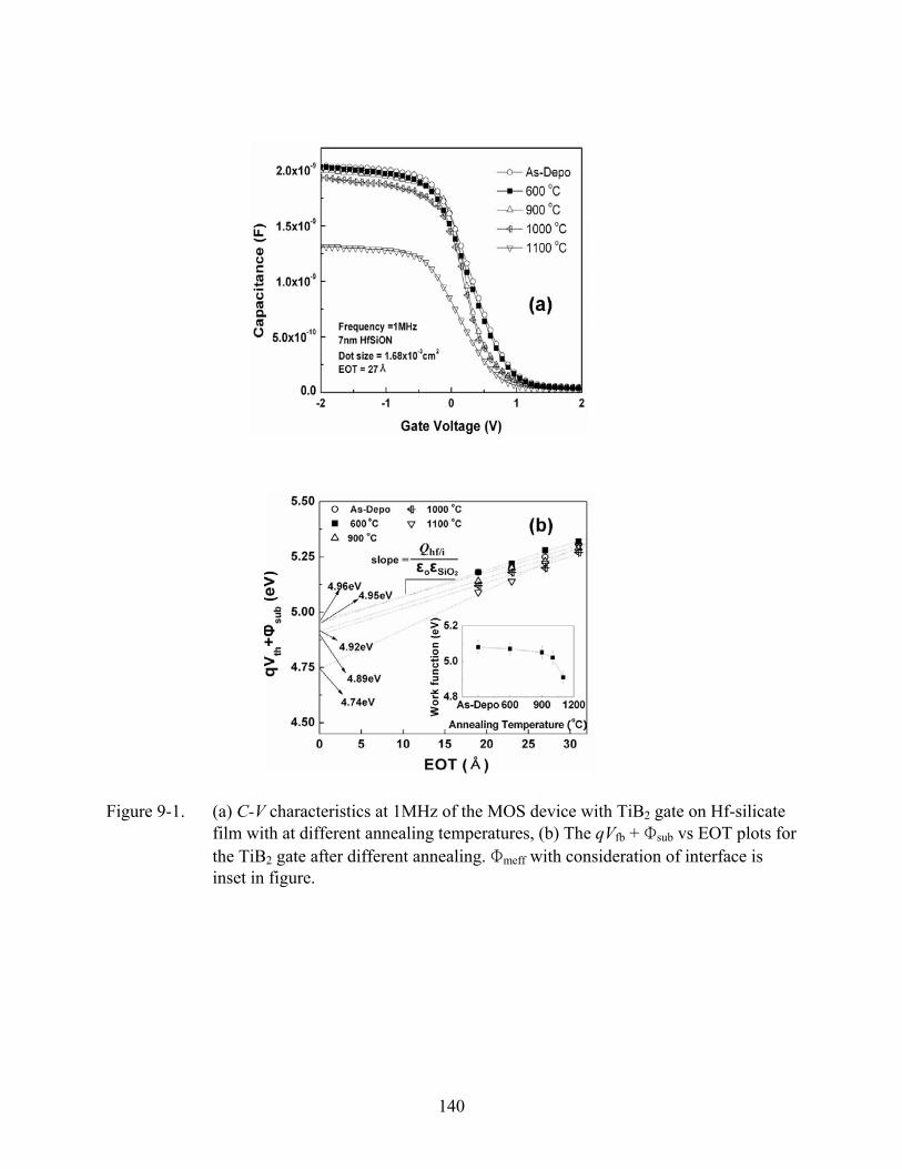
Figure 9-1. (a) C-V characteristics at 1MHz of the MOS device with TiB2 gate on Hf-silicate film with at different annealing temperatures, (b) The qVfb + Φsub vs EOT plots for the TiB2 gate after different annealing. Φmeff with consideration of interface is inset in figure.
140
Figure 9-2. AES depth profiles of Au/Ti/TiB2/Hf-silicate/Si MOS structure as a function of annealing temperature.
141
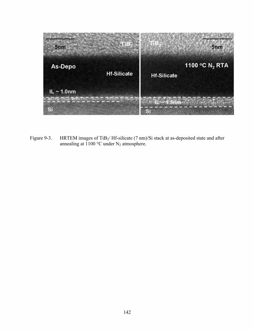
Figure 9-3. HRTEM images of TiB2/ Hf-silicate (7 nm)/Si stack at as-deposited state and after annealing at 1100 °C under N2 atmosphere.
142
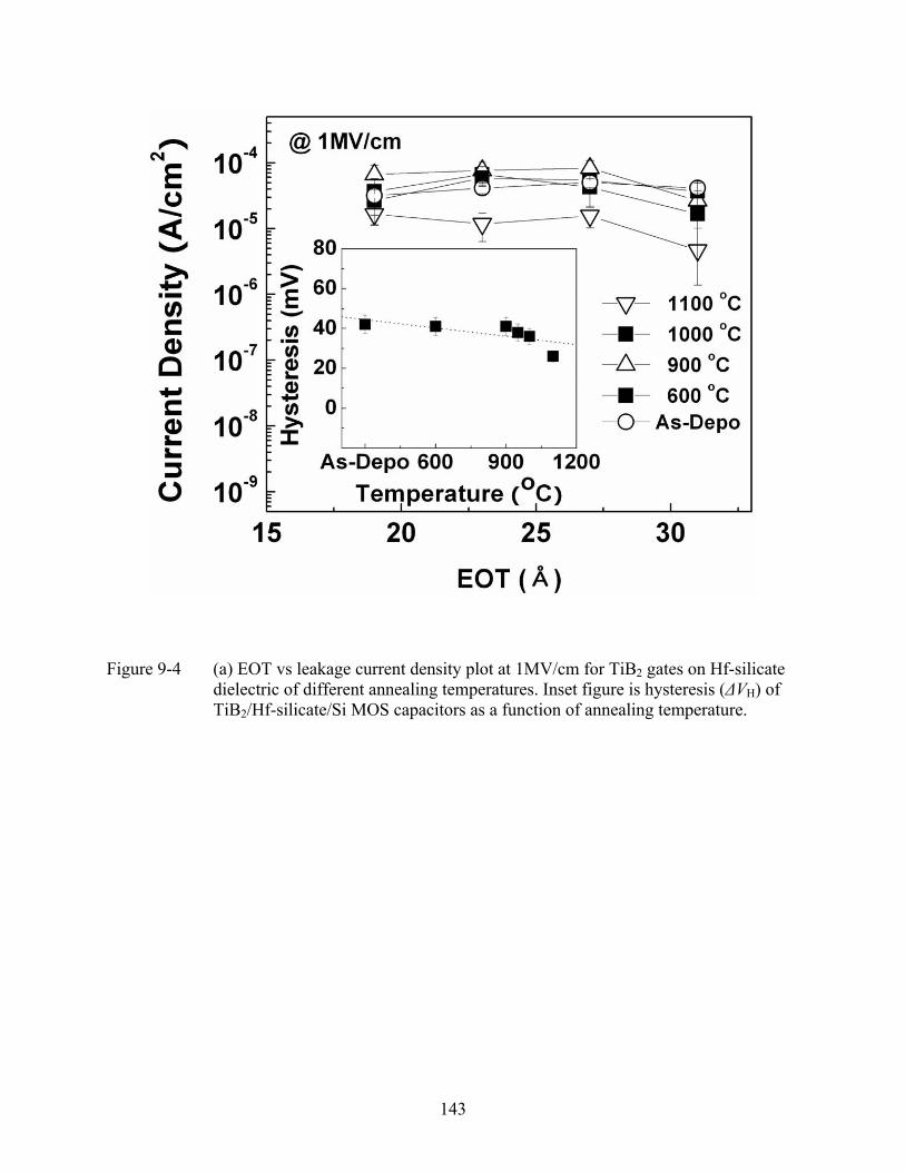
Figure 9-4 (a) EOT vs leakage current density plot at 1MV/cm for TiB2 gates on Hf-silicate dielectric of different annealing temperatures. Inset figure is hysteresis (ΔVH) of TiB2/Hf-silicate/Si MOS capacitors as a function of annealing temperature.
143
CHAPTER 10 STRAIN INDUCED CHANGES IN GATE LEAKAGE CURRENT AND DIELECTRIC
CONSTANT OF NITRIDED HF-SILICATE DIELECTRIC SILICON MOS CAPACITORS
Uniaxial–mechanical–strain altered gate leakage current and dielectric constant of silicon
metal–oxide–semiconductor (MOS) device with nitrided Hf-silicate gate dielectric are measured.
Uniaxial stress is applied using four–point wafer bending along [110] direction. The gate leakage
current and dielectric constant are found to increase by up to ~2 % under tensile and compressive
stress direction. The decrease in interface trap activation energy is used to explain leakage
current increment under mechanical stress. Doped nitrogen in Hf-silicate dielectric film occur N
p band splitting resulting increase in electronic polarization and decrease in dielectric constant.
Introduction
Hafnium silicate has been extensively studied as a gate dielectric material in advanced
metal oxide field effect transistors (MOSFETs) due to high crystallization temperature,
thermodynamic stability with Si, high permittivity and relatively large band gap (5.68 eV). 4,12,92-
100 Nitrogen incorporated Hf-silicate (HfSiON) has received attention since HfSiON minimizes
interface layer formation and reduces boron diffusion from the poly-Si gate.92-100 Also, recent
reports have addressed additional advantages of HfSiON dielectric such as increase in dielectric
constant and improvement of reliability.151,152 Therefore, HfSiON is among the top candidates to
be introduced as first generation high-k gate dielectric beyond the 45 nm era.151,152However, due
to the large remote phonon scattering, channel mobility degradation of MOSFET device with
high–k is unavoidable.153 In order to compensate the mobility degradation, strain engineering has
been introduced and explored as a promising technology.154 Recently, Thompson et al have
shown that mechanical stress induced channel mobility of MOSFET device with Hf-silicate
dielectric is similar to intrinsic channel mobility of MOSFET device with SiO2 gate
144
dielectric.155,156 However, to date, there is no systematic and quantitative result about strain effect
on dielectric constant and gate leakage current of HfSiON dielectric film.
In this work, we report, the effect of uniaxial stress on gate leakage current and dielectric
constant of Si MOS capacitors with HfSiON gate dielectric using controlled external applied
mechanical stress by 4- point bending method.
Experimental Detail
HfSiOx films were deposited directly on p-type (100) pre-cleaned (1% HF solution and DI
water rinse) 8 inch Si substrates with a resistivity of 3-25 Ωcm using atomic layer deposition
(ALD) at 300oC. SiH[N(CH3)2]3 is used as Si precursor where as Hf(NEtMe)4 (TEMAH) is
employed as Hf precursor. The oxidizing agents for TEMAH and Si are O3 and H2O,
respectively. HfSiOx film deposition is followed by nitrogen incorporation by rapid thermal
anneal (RTA) at 650 oC in NH3 ambience for 60 s. MOS capacitors with Pt and Al gate electrode
are fabricated using RF magnetron sputtering. All of the metals are deposited by Ar plasma
assisted rf sputtering at a pressure of 15 mTorr and 150W rf (13.56 MHz) power. For all MOS
devices, post metallization annealing (PMA) was carried out in tube furnace at 400oC in forming
gas (10% H2 / 90% N2) ambience for 30 min. Capacitance-voltage (C-V) and current-voltage (J-
V) measurements are performed with Agilent E4980A and Keithley 4200, respectively, using
controlled external mechanical stress along [110] direction.157 To extract the frequency-
independent device capacitance value and eliminate the effect of both series and shunt parasitic
resistances, two-frequency method is adopted.158 All C-V measurements are evaluated by NCSU
program.159 To reduce the electrical instability from HfSiON charging 160, constant gate voltage
(-1V) is applied for 160 s. The reduced instability allows monitoring of the strain-induced
change in gate leakage current.
145
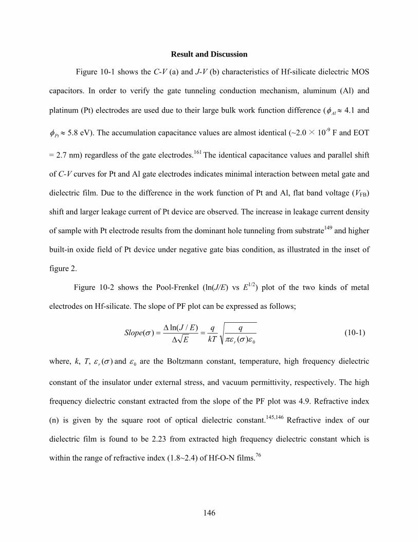
Result and Discussion
Figure 10-1 shows the C-V (a) and J-V (b) characteristics of Hf-silicate dielectric MOS
capacitors. In order to verify the gate tunneling conduction mechanism, aluminum (Al) and
platinum (Pt) electrodes are used due to their large bulk work function difference ( Alφ ≈ 4.1 and
Ptφ ≈ 5.8 eV). The accumulation capacitance values are almost identical (~2.0 × 10⁻⁹ F and EOT
= 2.7 nm) regardless of the gate electrodes.161 The identical capacitance values and parallel shift
of C-V curves for Pt and Al gate electrodes indicates minimal interaction between metal gate and
dielectric film. Due to the difference in the work function of Pt and Al, flat band voltage (VFB)
shift and larger leakage current of Pt device are observed. The increase in leakage current density
of sample with Pt electrode results from the dominant hole tunneling from substrate149 and higher
built-in oxide field of Pt device under negative gate bias condition, as illustrated in the inset of
figure 2.
Figure 10-2 shows the Pool-Frenkel (ln(J/E) vs E1/2) plot of the two kinds of metal
electrodes on Hf-silicate. The slope of PF plot can be expressed as follows;
0r )()/ln()(
εσπεσ q
kTq
EEJSlope =
ΔΔ
= (10-1)
where, k, T, )(σε r 0and ε are the Boltzmann constant, temperature, high frequency dielectric
constant of the insulator under external stress, and vacuum permittivity, respectively. The high
frequency dielectric constant extracted from the slope of the PF plot was 4.9. Refractive index
(n) is given by the square root of optical dielectric constant.145,146 Refractive index of our
dielectric film is found to be 2.23 from extracted high frequency dielectric constant which is
within the range of refractive index (1.8~2.4) of Hf-O-N films.76
146
The strain altered gate leakage currents for Al and Pt devices are shown in figure 10-3.
Regardless of electrodes, leakage current density in 2.7 MV/cm gate field increase under both
tensile and compressive stresses. Recently, Choi et al have suggested that interface trap
activation energy of SiO2/Si interface decreased with both tensile and compressive stress causing
increase in trap-assisted gate leakage current.156 Since Si-O predominant bonding characteristics
at Hf-silicate/Si interface has been reported 114-118, similar explanation can be applied to Hf-
silicate dielectric. Si-O predominant interface bonding mainly contribute trap-assisted
conduction in gate leakage current. Therefore, the applied strain changes the interface trap
activation energy, resulting in an increase in leakage current.
The relative changes in strain altered dielectric constant of HfSiON, HfSiOx(nitrogen
undoped Hf-silcate) and HfO2 film are shown in Figure 10-4. Unlike HfO2 and HfSiOx, the
dielectric constant of HfSiON increases with both tensile and compressive stresses, cross-
checked by C-V curve and slope extraction from PF plot. We believe that the incorporated
nitrogen in Hf-silicate film can be the origin of the strain-induced dielectric constant change.
Even though an exact explanation is not provided yet, strain induced N p band splitting is a
possible explanation. The N p band splitting by external strain increases the electronic transition
from the N p band to conduction band, which leads to band gap narrowing of HfSiON.160,161 The
strain-induced band gap narrowing affects electronic polarization, which related with high
frequency dielectric constant, resulting in an increased dielectric constant of HfSiON.161
Conclusion
Effect of mechanical stress on silicon metal-oxide-semiconductor capacitor with nitrided
Hf-silicate dielectric has been studied. The gate leakage current and dielectric constant was
found to be increase by up to ~2 % of both tensile and compressive stresses. Increase in leakage
current came from decreased HfSiON/Si interface trap activation energy. The fact that dielectric
147
constant variations under stress showed similar behavior by two different methods indicated the
increase in dielectric constant could be caused by increase in electronic polarization from N p
band splitting. Measurements of gate leakage current and dielectric constants of HfSiON
dielectric film under two different mechanical stress conditions provides quantitative results and
reveals that the incorporated nitrogen in the Hf-silicate film is a origin of dielectric constant
variation.
148
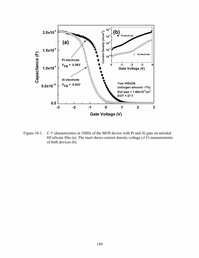
Figure 10-1. C-V characteristics at 1MHz of the MOS device with Pt and Al gate on nitrided Hf-silicate film (a). The inset shows current density-voltage (J-V) measurements of both devices (b).
149
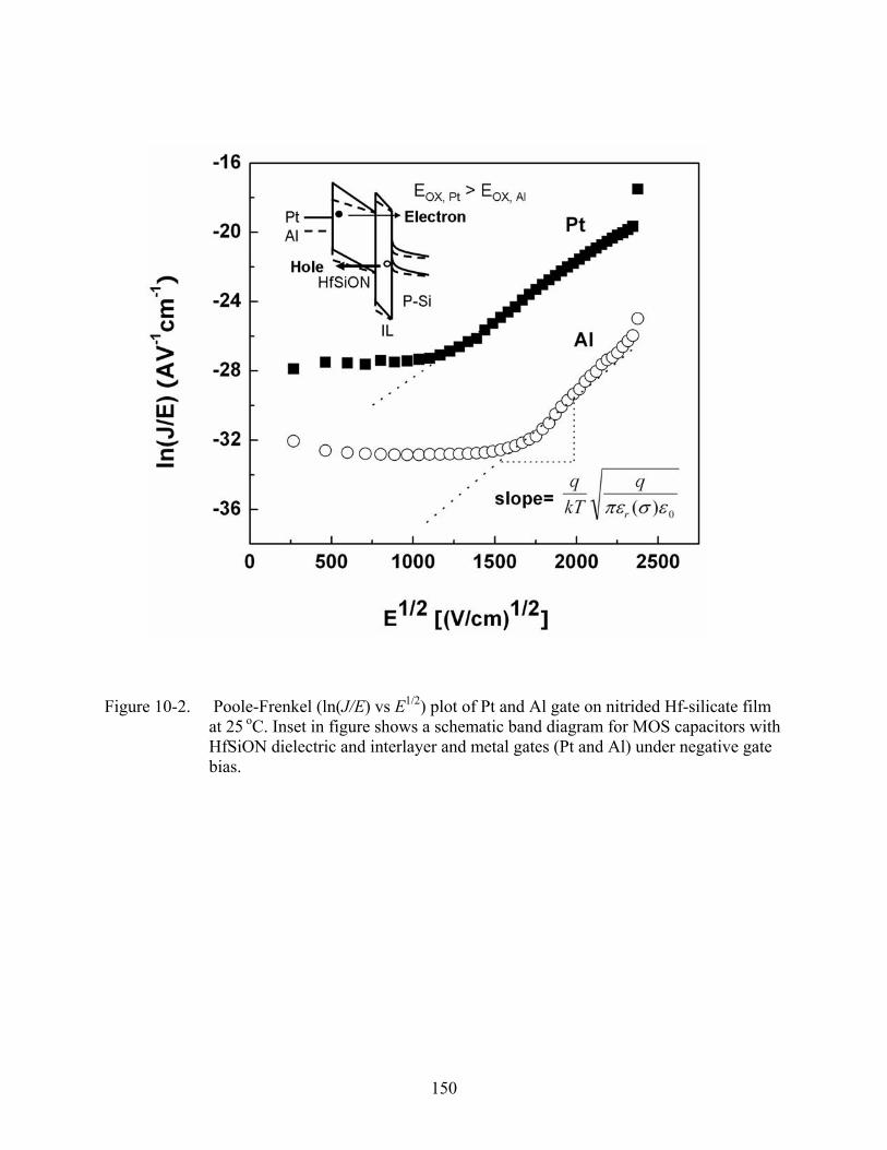
Figure 10-2. Poole-Frenkel (ln(J/E) vs E1/2) plot of Pt and Al gate on nitrided Hf-silicate film at 25 oC. Inset in figure shows a schematic band diagram for MOS capacitors with HfSiON dielectric and interlayer and metal gates (Pt and Al) under negative gate bias.
150
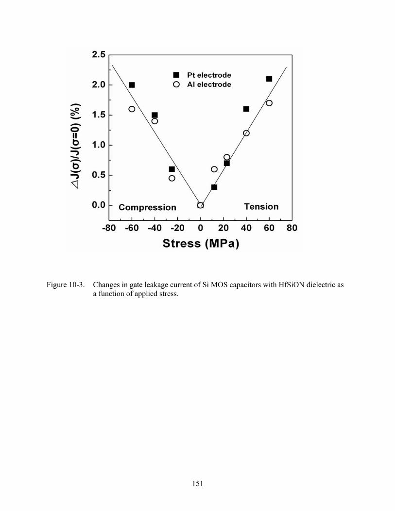
Figure 10-3. Changes in gate leakage current of Si MOS capacitors with HfSiON dielectric as a function of applied stress.
151
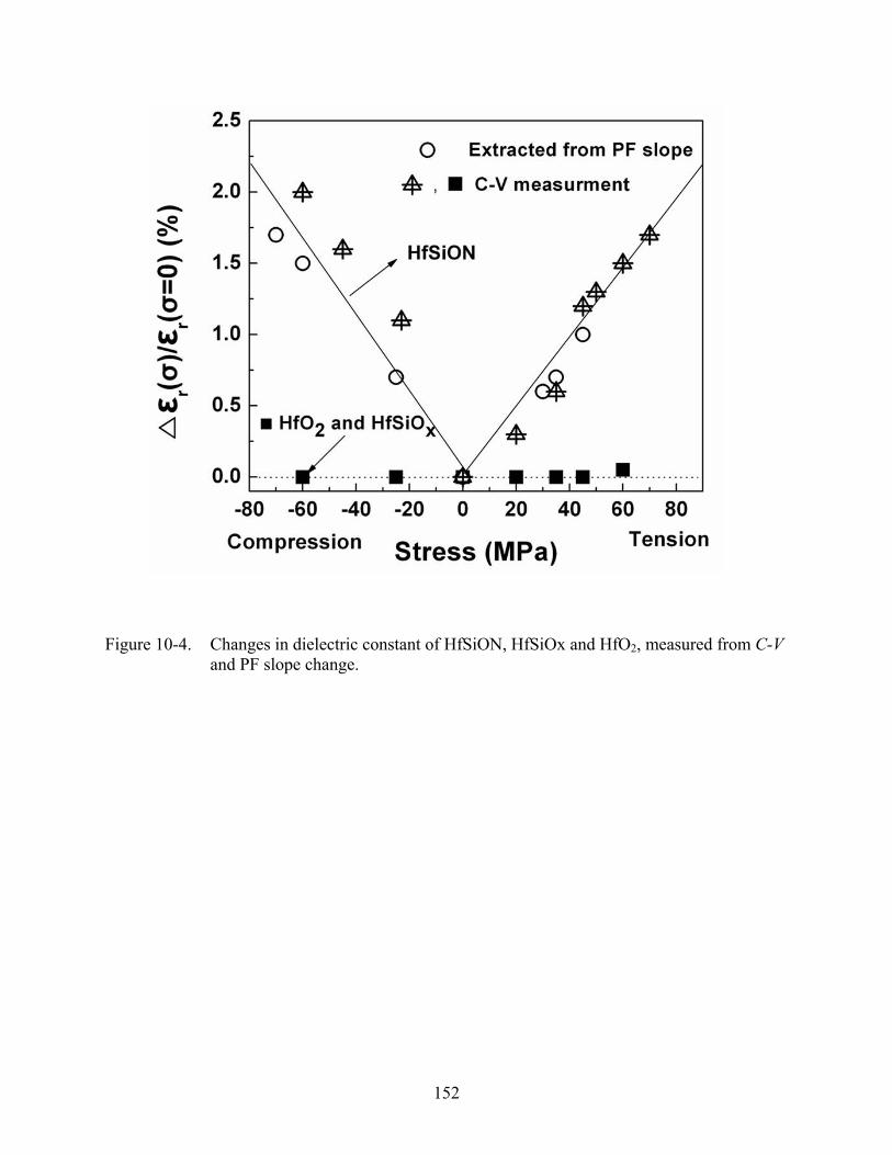
Figure 10-4. Changes in dielectric constant of HfSiON, HfSiOx and HfO2, measured from C-V and PF slope change.
152
CHAPTER 11 CONCLUSIONS
The effect of temperature in thermal nitridation process on physical structure of the IL was
investigated using XRR studies. At high nitridation temperatures, the nitridation efficiency
increased leading to increase in IL roughness apart from increase in film and IL density and IL
thickness. There was a general improvement in the electrical properties of films at higher
nitridation temperature till the degradation of interface quality due to interface roughening led to
degradation of some of the electrical properties. An excessive nitrogen piling up at IL of 850 oC
nitrided Hf-silicate resulted in nonuniform distribution of nitrogen and oxide charge, high
roughness IL and degradation of Dit, electron channel mobility and breakdown resistance.
Therefore, the quantitative results of IL roughness by XRR study showed reliable
correspondence with electrical results and can have a potential as an analysis tool of thin film
structure.
To suppress the thermal nitridation induced interface degradation, the UV assisted low
temperature nitrogen doping technique for hafnia gate dielectric film was investigated. The
incorporation efficiency of UV assisted low temperature method was comparable to the high
temperature (~650 oC) thermal nitridation process. Moreover, due to the low process temperature
and multiplicity of dissociation species, uniform distribution of nitrogen and oxygen, thinner
interface layer (10 Å), higher capacitance value (3.69 µF/cm2) and smaller EOT (9.4 Å) were
observed in the case of UV assisted low temperature nitrided sample.
By using UV assisted low temperature nitrided Hf-silicate film, in order to address the
possibility of dual gate device application, MOS device with Ti, TiN and TiB2 gate electrodes
were examined. Considering EOTi and Qhk/i, the extracted Φmeff values for Ti, TiN and TiB2 gate
were 4.27, 4.56 and 5.08 eV, respectively. Regardless of gate electrodes, the conduction
153
154
mechanism of the samples well fitted with Poole-Frenkel conduction model and conduction
activation energies showed almost identical values (~ 1.7 eV). Therefore, Ti gate electrode is
more favorable for NMOS device and TiB2 gate electrode can be used for PMOS with Hf-silicate
dielectrics
Furthermore, in order for successful implements to future CMOS devices, thermal stability
also should be confirmed. The extracted Φmeff values for TiB2 gate was almost identical (5.07 eV)
till 1000 oC annealing treatments. The Φmeff lowering phenomena (4.91 eV) was observed when
annealed at 1100 oC, due to the metal and Hf-silicate intermixing by material transfer and
electron transfer by oxygen vacancy generation. The leakage current density of TiB2 electrode
MOS device were lower than ~ 10-4 A/cm2 and ΔVH is reduced after 1100 oC annealing. The
possibility of TiB2 gate metal for the PMOS application was confirmed. The long term stability
of boride and process compatibility remains to be established.
Finally, since future CMOS device will adopt the strained MOSFET structure, an effect of
mechanical stress on silicon metal-oxide-semiconductor capacitor with nitrided Hf-silicate
dielectric has been studied. The gate leakage current and dielectric constant was found to be
increase by up to ~2 % of both tensile and compressive stresses. Increase in leakage current came
from decreased HfSiON/Si interface trap activation energy. The fact that dielectric constant
variations under stress showed similar behavior by two different methods indicated the increase
in dielectric constant could be caused by increase in electronic polarization from N p band
splitting. Measurements of gate leakage current and dielectric constants of HfSiON dielectric
film under two different mechanical stress conditions provides quantitative results and reveals
that the incorporated nitrogen in the Hf-silicate film is a origin of dielectric constant variation.
LIST OF REFERENCES
1. D. R. Askeland and P. P. Phule, The Science and Engineering of Materials, 4th ed. (Brooks
Cole Publishing Company, St. Paul, Minnesota 2002).
2. T. Hori Gate Dielectrics and MOS ULSIs (Springer Series in Electronics and Photonics 34)
3. S. M. Sze, Physics of Semiconductor Devices, 2nd ed. (Wiley, New York, 1981).
4. G. D. Wilk, R. M. Wallace, and J. M. Anthony, J. Appl. Phys. 89, 5243 (2001).
5. International Technology Roadmap for Semiconductors, 2002 edition
6. J. D. Plummer and P. B. Griffin, Proceedings of the IEEE 89, 240 (2001).
7. D. A. Buchanan, IBM, J. Res. Develop., vol. 43, pp. 245-264, (1999).
8. J. H. Stathis, IEEE Transactions on Device and Materials Reliability, 1, pp. 43 -59, (2004)
9. J. H. Stathis and D. J. DiMaria, IEEE International Electron Devices Meeting, pp. 167, (1998).
10. Y. J. Jeon, B. H. Lee, K. Zawadzki, W. J. Qi, A. Lucas, R. Nieh and J. Lee, IEDM Tech. Dig., pp.797, (1998).
11. B. Cheng, M. Cao, R. Rao, A. Inani, V. Voorde, W. M. Greene, J. M. C Stork, Y. Zhiping, P. M. Zeitzoff, J. C. S. Woo, Electron Devices, IEEE Transactions on , Vol. 46 , pp.1537 – 1544, (1999).
12. C. H. Lee, H. F. Luan, W. P. Bai, S. J. Lee, T. S. Jeon, Y. Senzaki, D. Roberts, and D. L. Kowng, IEDM Tech. Dig., pp. 27-30, (2000).
13. L. Kang, K. Onishi, Y. J. Jeon, B. H. Lee, C. S.Kang, W. Qi, R. Nieh, S. Gopalan, R. Choi, and J. C. Lee, IEDM Tech. Dig., pp. 35, (2000).
14. K. Onishi, L. Kang, R. Choi, E. Dharmarajan, S. Gopalan, Y.J. Jeon, C, S, Kang, B, H, Lee, R. Nieh, and J. C. Lee, VLSI Tech. Dig., p.131 , (2001).
15. R. Choi, C. S. Kang, B. H. Lee, K. Onishi, R. Nieh, S. Gopalan, E. Dharmarajan and J. C. Lee, VLSI Tech. Dig., pp. 15, (2001).
16. Q. Lu, H. Takeuchi, X. Meng, T. J. King, C. Hu, K.Onishi, H.-J. Cho, J. Lee, VLSI Tech. Dig., pp. 86 -87, (2002).
17. K. J. Hubbard and D. G. Schlom, J. Mat. Res. 11, 2757 (1996).
18. J. J. Chambers and G. N. Parsons, J. Appl. Phys. 90, 918 (2001).
155
19. D. G. Schlom and J. H. Haeni, Mat. Res. Soc. Bulletin 27, 198 (2002).
20. A. Chatterjee, R. A. Chapman, K. Joyner, M. Otobe, S. Hattangady, M. Bevan, G. A. Brown, H. Yang, Q. He, D. Rogers, Tech. Dig. Int. Electron Devices Meet, pp. 777, (1998).
21. P. K. Roy and I. C. Kizilyalli, Appl. Phys. Lett. 72, 2835, (1998).
22. I. C. Kizilyalli, R. Y. S. Huang, and P. K. Roy, IEEE Electron Device Lett. 19, 423 (1998).
23. Q. Lu, D. Park, A. Kalnitsky, C. Chang, C. C. Cheng, S. P. Tay, Y.-C. King, T.-J. King, C. Hu, IEEE Electron Device Lett. 19, 341, (1998).
24. D. Park, Y.-C. King, Q. Lu, T.-J. King, C. Hu, A. Kalnitsky, S.-P. Tay, and C.-C. Cheng, IEEE Electron Device Lett. 19, 441 (1998).
25. H. F. Luan, B. Z. Wu, L. G. Kang, B. Y. Kim, R. Vrtis, D. Roberts, and D. L. Kwong, Tech. Dig. Int. Electron Devices Meet, pp. 609 (1998).
26. C. W. Liu, S. Maikap and C. Y. Yu, IEEE circuit & Device magazine pp 21-33, (2005)
27. M. H. Lee, P. S. Chen, W.-C. Hua, C.-Y. Yu, Y.-C. Lee, S. Maikap, Y.M. Hsu, C.W. Liu, S.C. Lu, W.-Y. Hsieh, and M.-J. Tsai, Proc. Int. SiGe Technol. And Device Meet. (ISTDM), Frankfurt, Germany, pp. 87–88, (2004).
28. M. L. Lee and E. A. Fitzgerald, IEDM Tech. Dig., pp. 429–432, (2003).
29. R. Oberhuber, G. Zandler, and P. Vogl, Phys. Rev.B, 58, pp. 9941–9947, (1998).
30. M. R. Viscokay, J. J. Chambers, A. L. P. Rotondaro, A. Shanware and L. Colombo, Appl. Phys. Lett. 80 3138 (2002).
31. M. Balog, M. Schieber, M. Michman, and S. Patai, J.of Electrochem.Soc. 126, pp.1203-1207 (1979).
32. W. B. Bluementhal, The Chemical Behavior of Zirconium (Van Nostrand, Princeton, 1958).
33. L. Kang, B. H. Lee, W. J. Qi, Y. Jeon, R. Nieh, S. Gopalan, K. Onishi, and J. C. Lee, IEEE Electron Device Letters 21, pp.181-183 (2000).
34. S. W. Nam, J. H. Yoo, S. Nam, H. J. Choi, D. Lee, D. H. Ko, J. H. Moon, J. H. Ku, and S. Choi, J. Non-Crystalline Solids 303, 139-143 (2002).
35. B. H. Lee, L. Kang, W. J. Qi, R. Nieh, Y. Jeon, K. Onishi, and J. C. Lee, IEDM Tech. Dig., 133-136 (1999).
36. Q. Fang, J. Y. Zhang, Z. M. Wang, J. X. Wu, B. J. O'Sullivan, P. K. Hurley, T. L. Leedham, H. Davies, M. A. Audier, C. Jimenez, J. P. Senateur, and I. W. Boyd, Thin Solid Films 428, 263-268 (2003).
156
37. G. D. Wilk and R. M. Wallace, Appl. Phys. Lett. 74, pp 2854-2856 (1999).
38. S. Van Elshocht, U. Weber, T. Conard, V. Kaushik, M. Houssa, S. Hyun, B. Seitzinger, P. Lehnen, M. Schumacher, J. Lindner, M. Caymax, S. De Gendt, and M. Heyns, J.of Electrochem.Soc. 152, F185-F189 (2005).
39. G. Pant, A. Gnade, M. J. Kim, R. M. Wallace, B. E. Gnade, M. A. Quevedo-Lopez, P. D. Kirsch, and S. Krishnan, Appl. Phys. Lett. 89, 032904, (2006).
40. P. D. Kirsch, C. S. Kang, J. Lozano, J. C. Lee, and J. G. Ekerdt, J. Appl. Phys. 91, pp4353-4363 (2002).
41. S. Inumiya, K. Sekine, S. Niwa, A. Kaneko, M. Sato, T. Watanabe, H.Fukui,Y. Kamata, M. Koyama, A. Nishiyama, M. Takayanagi, K. Eguchi and Y.Tsunashima, VLSI Tech. Dig., pp.17-18 (2003).
42. T. Watanabe, M. Takayanagi, R. Iijima, K. Ishimaru, H. Ishiuchi and Y. Tsunashima, VLSI Tech. Dig., pp. 19-20 (2003).
43. M. R.Visokay, J. J.Chamber, A. L .P.Rotondaro, R. Kuan, L.Tsung, M. Douglas, M. J. Bevan, H. Bu, A. Shanware, and L. Colombo, Proceedings of 3rd International Conference on Microelectronics and Interfaces, pp.127-129, (2002).
44. M. Koyama, A. Kaneko, T. Ino, M. Koike, Y. Kamata, R.Iijima, Y. Kamimuta, A. Takashima, M. Suzuki, C. Hongo, S. Inumiya, M. Takayanagi, and A. Nishiyama, IEDM Tech. Dig., pp. 849 -852 (2002).
45. Y. G. Fedorenko, L. Truong, V. V. Afanas'ev, A. Stesmans, Z. Zhang, and S. A. Campbell, J. Appl. Phys. 98, 123703 (2005).
46. E. M. Young and W. A. Tiller, J. Appl. Phys. 662, 2086 (1987).
47. I. W. Boyd, V. Craciun, and A. Kazor, Jap. J. of Appl. Phys. 32, 6141-6146 (1993).
48. D. L. Baulch, R. A. Cox, R. F. Hampson, J. A. Kerr, J. Troe, and R. T. Watson, J. of Phys. and Chem. 9, 295-471 (1980).
49. S. Ramanathan, G. D. Wilk, D. A. Muller, C. M. Park, and P. C. McIntyre, Appl. Phys. Lett. 79, 2621 (2001).
50. S. Ramanathan, C. M. Park, and P. C. McIntyre, J. Appl. Phys. 91, 4521 (2002).
51. S. Ramanathan, D. Chi, P. C. McIntyre, C. J. Wetteland, and J. R. Tesmer, J. of the Electrochem. Soc. 150, F110 (2003).
52. P. Punchaipetch, G. Pant, M. J. Kim, R. M. Wallace, and B. E. Gnade, J. Vac. Sci. Tech. A 22, 395 (2004).
157
53. B. Maiti, P.J. Tobin, SPIE Conference on Microelectronic Device Technology III, SPIE vol. 3881 46 (1999).
54. I. De, D. Johri, A. Srivastava, C.M. Osburn, Solid State Electronics, 44, 1077 (2000)
55. B. Cheng, B. Maiti, S. Samavedam, J. Grant, B. Taylor, P. Tobin, J. Mogab, 2001 IEEE Intl. SOI Conf., (2001).
56. H. Pierson, Handbook of Refractory Carbides and Nitrides, (Noyes, 1996)
57. P. Ranade, H. Takeuchi, T-J. King, C. Hu, Electrochem. Sol. State Lett., 4 G85 (2001).
58. J. K. Schaeffer, S. B. Samavedam, D. C. Gilmer, V. Dhandapani, P. J. Tobin, J. Mogab, B-Y. Nguyen, B. E. White Jr., S. Dakshina-Murthy1, R. S. Rai, Z. -X. Jiang, R. Martin, M. V. Raymond, M. Zavala, L. B. La, J. A. Smith, R. Garcia, D. Roan, M. Kottke2, and R. B. Gregory2., J. Vac. Sci. Tech. B 21 (2003)
59. Y. Saito, S. Kawata, H. Nakane, H. Adachi, Appl. Surf. Sci. 146 177 (1999).
60. C. S. Kang, H.-J. Cho, Y. H. Kim, R. Choi, K. Onishi, A. Shahriar, J. C. Lee J. Vac. Sci. Tech. B 21 5 (2003).
61. M. Moriwaki, T. Yamada, Jpn. J. Appl. Phys., 40 2679 (2001).
62. D-G. Park, H-J. Cho, K-Y. Lim, T-H. Cha, I-S. Yeo, J-W. Park, J. Electrochem. Soc., 148 F189 (2001).
63. D-G. Park, K-Y. Lim, H-J. Cho, T-H. Cha, J-J. Kim, J-K. Ko, I-S. Yeo, J-W. Park, VLSI Tech. Dig., (2001).
64. H.Y. Yu, H.F. Lim, J.H. Chen, M.F. Li, C. Zhu, C.H. Tung, A.Y. Du, W.D. Wang, D.Z. Chi, D.-L. Kwong, IEEE Elec. Dev. Lett., 24, 4 (2003).
65. M.-A. Nicolet, P.H. Giauque, Microelectronic Engr., 55, 357 (2001).
66. Y-S. Suh, G. Heuss, V. Misra, J. Vac. Sci. Tech. B, 22, 1 (2004).
67. R. Li, Q. Xu, Trans. Electron Devices, 49, 11 (2002).
68. S. B. Samavedam, L. B. La, J. Smith, S. Daksha-Murthy, E. Luckowski, J. Schaeffer, M. Zavala, R. Martin, V. Dhandapani, D. Triyoso, H. H. Tseng, P. J. Tobin, D. C. Gilmer, C. Hobbs, W. J. Taylor, J. M. Grant, R. Hegde, J. Mogab, C. Thomas, P. Abramowitz, M. Moosa, J. Conner, J. Jiang, V. Aruachalam, M. Sadd, B-Y. Nguyen and B. White, IEDM Tech. Dig., 433-436, (2002).
69. J-H. Lee, H. Zhong, Y-S. Suh, G. Heuss, J. Gurganus, B. Chen, V. Misra, IEDM Tech. Dig. 359-362, (2002)
70. V. Misra, H. Zhong, H. Lazar, IEEE Electron Dev. Lett., 23 6 (2002).
158
71. I. Polishchuk, P. Ranade, T-J. King, C. Hu, IEEE Electron Dev. Lett., 22 9 (2001).
72. B-Y. Tsui, C-F. Huang, IEEE Electron Dev. Lett., 24 3 (2003).
73. Q. Lu, R. Lin, P. Ranade, T-J. King, C. Hu, IEEE VLSI Symp., pp 45 (2004).
74. H. Wakbayashi, Y. Saito, K. Takeuchi, T. Mogami, T. Kunio, IEEE Trans. Electron Dev., 48 2363 (2001)
75. R.T. Tung, Mat. Sci. Engr. R, 35 1-138 (2001).
76. C. Hobbs, L. Fonseca, V. Dhandapani, S. Samavedam, B. Taylor, J. Grant, L. Dip, D. Triyoso, R. Hegde, D. Gilmer, R. Garcia, D. Roan, L. Lovejoy, R. Rai, L. Hebert, H. Tseng, B. White and P. Tobin, VLSI Tech. Dig., (2003)
77. Y. C. Yeo, T. J. King, C. Hu, J. Appl. Phys. 92 12 7266 (2002).
78. H. Hasegawa, H. Ohno, J. Vac. Sci. Tech. B 4, 1130 (1986).
79. J. L. Freeouf, J.M. Woodall, Appl. Phys. Lett. 39, 727 (1981).
80. K. Rim, J. Chu, H. Chen, K.A. Jenkins, T. Kanarsky, K. Lee, A. Mocuta, H. Zhu, R. Roy, J. Newbury, J. Ott, K. Petrarca, P. Mooney, D. Lacey, S. Koester, K. Chan, D. Boyd, M. Ieong, and H.-S. Wong, VLSI Tech. Dig., pp. 98–99, (2002).
81. K.C. Liu, X. Wang, E. Quinones, X. Chen, X.D. Chen, D. Kencke, B. Anantharam, R.D. Chang, S.K. Ray, S.K. Oswal, and S.K. Banerjee, IEDM Tech. Dig., pp.63–66, (1999).
82. X. Wang, D.L. Kencke, K.C. Liu, A.F. Tasch, L.F. Register, and S. K. Banerjee, Proc. IEEE Int. Conf. Simulation of Semicond. Process. and Dev., pp.70–73 (2002).
83. K. Mistry, M. Armstrong, C. Auth, S. Cea, T. Coan, T. Ghani, T. Hoffmann, A. Murthy, J. Sandford, R. Shaheed, K. Zawadzki, K. Zhang, S. Thompson, and M. Bohr, Symp. VLSI Tech. Dig., pp. 50–51 (2004).
84. M.D. Giles, M. Armstrong, C. Auth, S.M. Cea, T. Ghani, T. Hoffmann, R. Kotlyar, P. Matagne, K. Mistry, R. Nagisetty, B. Obradovic, R. Shaheed, L. Shifren, M. Stettler, S. Tyagi, X. Wang, C. Weber, and K. Zawadzki, Symp. VLSI tech. Dig., pp. 118–119 (2004).
85. G. Scott, J. Lutze, M. Rubin, F. Nouri, and M. Manley, IEDM Tech. Dig., pp. 827–830 (1999).
86. S. Pidin, T. Mori, R. Nakamura, T. Saiki, R. Tanabe, S. Satoh, M. Kase, K. Hashimoto, and T. Sugii, Symp. VLSI Tech. Dig., pp. 54–55 (2004).
87. T. Ghani, M. Armstrong, C. Auth, M. Bost, P. Charvat, G. Glass, T. Hoffmann, K. Johnson, C. Kenyon, J. Klaus, B. McIntyre, K. Mistry, A. Murthy, J. Sandford, M. Silberstein, S. Sivakumar, P. Smith, K. Zawadzki, S. Thompson, and M. Bohr, IEDM Tech Dig., pp. 978–980 (2003).
159
88. R. E. Beaty, IEEE Trans. Components, Hybrids and Manufacturing Technology, (1992).
89. T. Chen and Y.-R. Huang, IEEE Trans. Components and Packaging Technologies, (2002).
90. J. J. Wortman and R. A. Evans, J. Appl. Phys., 36, pp. 153-156, (1965).
91. K. Yamamoto, S. Hayashi, and M. Niwa, Appl. Phys. Lett. 83, 11 (2003).
92. J. F. Kang, H. Y. Yu, C. Ren, M.-F. Li, D. S. H. Chan, H. Hu, H. F. Lim, W. D. Wang, D. Gui, and D.-L. Kwong, Appl. Phys. Lett. 84, 1588 (2004).
93. P. K Park and S. W. Kang, Appl. Phys Lett 84, 19 (2006).
94. K. Ramani, C. R. Essary, S. Y. Son, V. Craciun and R. K. Singh, Appl. Phys. Lett 83, 242902 (2006).
95. R. C. Powell, N.-E. Lee, and J. E. Greene, Appl. Phys. Lett. 60, 2505 (1992).
96. M.-H. Cho, K. B. Chung and D.–W. Moon, Appl. Phys. Lett. 89, 182908 (2006).
97. J. Kim and K. Yong. J. Appl. Phys. 100, 044106 (2006).
98. C. Kang, P. Lysaght, R. Choi, B. Lee, S. Rhee, C. Choi, M. Akbar, and J. Lee, Appl. Phys. Lett. 86, 222906 (2005).
99. M. A. Quevedo-Lopez, M. El-Bouanani, M. J. Kim, B. E. Gnade, R. M. Wallace, M. R. Visokay, A. LiFatou, J. J. Chambers, and L. Colombo, Appl. Phys. Lett. 82, 4669 (2003).
100. M.-H. Cho, K. B. Chung, C. N. Whang, D.-H. Ko, J. H. Lee and N. I. Lee, Appl. Phys. Lett. 88, 202902 (2006).
101. M.-H. Cho, K. B. Chung, and D.-H. Ko, Appl. Phys. Lett. 89, 142908 (2006).
102. K. Ramani, P. Kumar, K. Siebein, V. Craciun, R. K. Singh, Electrochem. Solid-state Lett. 10, H66 (2007).
103. H. Kato, T. Nango, T. Miyagawa, T. Katagiri, K. S. Seol, and Y. Ohki, J. Appl. Phys., 92, 1106 (2002).
104. R. Thomas, E. Rije, P. Ehrhart, A. Milanov, R. Bhakta, A. Bauneman, A. Devi, R. Fischer, and R. Waser, J. Electrochem. Soc. 154, G77 (2007).
105. A. R. Teren, R. Thomas, J. He and P. Ehrhart, Thin Solid Film, 478, 206 (2005).
106. C. Sire, S. Blonkowski, M. J. Gordon, and T. Baron Appl. Phys. Lett. 91, 242905 (2007).
107. P. Fiorenza, R. L. Nigro, V. Raineri, S. Lombardo, R. G. Toro, G. Malandrino, and I. L. Fragala, Appl. Phys. Lett. 87, 231913 (2005).
160
108. J. L. Gavartin, A. L. Shluger, A. S. Foster, and G. I. Bersuker, J. Appl. Phys. 97, 053704 (2005).
109. K. Torii, K. Shirashi, S. Miyazaki, K. Yamabe, M. Boero, T. Chikyow, K. Yamada, H. Kitajima, and T. Arikado, IEEE IEDM 04, 129 (2004).
110. M. A. Quevedo-Lopez, S. A. Krishnan, P. D. Kirsch, G. Pant, B. E. Gnade, and R. M. Wallace, Appl. Phys. Lett. 87, 262902 (2005).
111. M.-T. Wang, B. Y.-Y. Cheng, and J. Y.-M. Lee Appl. Phys. Lett. 88, 242905 (2006).
112. S. J. Lee, H. F. Luan, C. H. Lee, T. S. Jeon, W. P. Bai, Y. Senzaki, D. Roberts, and D. L. Kwong, VLSI Tech. Dig., 2001 133
113. A. Deshpande, R. Inamn, G. Jursich and C. G. Takoudis, J. Appl. Phys. 99, 9 (2006)
114. C. C. Yeo, M. S. Joo, B. J. Cho and S. J. Whang, Thin Solid Films 463, 90-95 (2004)
115. B. Sen, C. K. Sarkar, H. Wong, M. Chan and C.W. Kok, Solid-State Electronics, 50, 237 (2006)
116. M. Lee, Z. –H. Lu, W. –T. Ng, D. Landheer, X. Wu and S. Moisa, Appl. Phys. Lett. 83, 2638 (2003)
117. V. Craciun and R. K. Singh, Appl. Phys. Lett. 76, 1932 (2000)
118. V. Craciun, R. K. Singh, J. Perriere, J. Spear and D. Craciun, J. Electrochem. Soc. 147, 1077 (2000)
119. A. Srivastava, V. Craciun, J. M. Howard and R. K. Singh, Appl. Phys. Lett. 75, 9002 (1999)
120. Z. Lencces, S. Guicciardi, C. Melandri, and A. Bellosi, Br. Ceram. Trans. 94, 38 (1995)
121. J. R. Hauser and K. Ahmed, AIP Conf. Proc. 449, 235 (1998).
122. C. D. Wagner, D. E. Passoja, H. F. Hillery, T. G. Kinisky, H. A. Six, W. T. Jansen, and J. A. Taylor, J. Vac. Sci. 21, 933 (1982)
123. J. M. Howard, V. Craciun, C. Essary, and R. K. Singh, Appl. Phys. Lett. 81, 3431 (2002)
124. J. H. Park, T. J. Park, M. J. Cho, S. K. Kim, S. H. Hong, J. H. Kim, M. H. Seo, C. S. Hwang, J. Y. Won, R. J. Jeong and J. H. Choi, J. Appl. Phys 99, 094501 (2006)
125. J. Kim, S. Kim, H. Kang, J. Choi, H. Jeon, M. Cho, K. Chung, S. Back, K. Yoo, and C. Bae, J. Appl. Phys. 98, 094504 (2005).
126. J. Heitz, H. Niino and A. Yabe, Appl. Phys. Lett. 68, 2648 (1996).
161
127. N. A .Chowdhury and D. Misra, J. Electrochem. Soc. 154, G30-G37 (2007).
128. R. K. Nahar, Vikram Singh and Aparna Sharma J. Mat. Sci Electron 18 615 (2007).
129. C. L. Cheng, K. C.-Liao, and T. Wang, Electrochem. Soc. Lett. 9 F80-F82, (2006).
130. Alfred Grill, Cold Plasma in Materials Fabrication Institute of Electrical and Electronics Engineers, Inc., New York, pp. 74–80, (1994).
131. Y. K. Chiou, C. H. Chang, C. C. Wang, K. Y. Lee, T. B. Wu, R. Kwo, and M. Hong J. Electrochemical Society, 154 G99-G102 (2007).
132. N. Ikarashi, K. Watanabe, K. Masuzaki, T. Nakagawa, and M. Miyamura, J. Appl. Phys 100, 063507 (2006).
133. C. R. Essary, K. Ramani, V. Craciun and R. K. Singh Appl. Phys. Lett. 88, 182902 (2006).
134. S. Toyoda, J. Okabayashi, H. Takahashi, M. Oshima, D. Lee, S. Sun, S. sun, P. A. Pianetta, T. Ando, and S. Fukuda, Appl. Phys. Lett 87, 182908 (2005).
135. F. J. Gruntharner, P. J. Gruntharner, R. P. Vasquez, B. F. Lewis, J. Maserjian, and A. Madhukar, Phys. Rev. lett. 43, 1683 (1979).
136. M. A. Nicolet, Thin Solid Films, 52, 415, (1978).
137. C. S. Choi, Q.Wang, M. Carlton , G. A. Ruggles, A.S. Shah, IEEE Transactions on Electron Devices, 39, 10, (1992).
138. R. Khanna, S. J. Pearton, F. Ren, I.I Kravchenko, Vac. Sci. Tech. B. 24(2006).
139. H. Yang, Y. Son, S. Baek, H. Hwang, H. Lim, H. S. Jung, Appl. Phys. Lett 86, 092107 (2005).
140. H. Yang, S. Heo, D. Lee, S. Choi and H. Hwang, Jpn. J. Appl. Phys. 45, 3 (2006).
141. R. Jha, J. Gurganos, Y. H. Kim, R. Choi and Jack Lee, IEEE Electron Devices Lett. 25, 6 (2004).
142. S. H. Bae, W. P. Bai, H. C. Wen, S. Mathew, L. K. Bera, N. Balasubramanian, N. Yamada, M. F. Li, and D. L. Kwong, Symp. VLSI tech. Dig., 188 (2004).
143. J. Westlinder, G. Sjoblom and J. Olsson, Microelectronic Engineering 75 (2004).
144. D. S. Jeong, H. B.Park and C. S. Hwang, Appl. Phys. Lett 86, 072903 (2005).
145. D. Eom, S. Y. No, C. S. Hwang, and H. J. Kim, J. Electrochem. Soc. 153, 4 (2006).
146. S. Y. Son, P. Kumar, J. S. Lee, H. Cho, H. S. Jung, K. J. Min, C. J. Kang, and R. K. Singh, Electrochem. Soc. Lett.11 H81 (2008).
162
147. Y. Akasaka, G. Nakamura, K. Shiraishi, N. Umezawa, K. Yamabe, O. Ogawa, M. Lee, T. Amiaka, T. Kasuya, H. Watanabe, T. Chikyow, F. Ootsuka, Y. Nara and K. Nakamura, Jpn. J. Appl. Phys. 45, L1289–L1292, (2006).
148. S. J. Doh, J. H. Lee, J. P. Kim, J.-H. Lee, Y.-S. Kim, H.-J. Lim, H.-S. Jung, S. K. Han, M. J. Kim, N.-I. Lee, H.-K. Kang, S. G. Park, and S. B. Kang, IEEE International Reliability Physics Symp., (2005)
149. Y. S. Suh, H. Lazar, B. Chen, J. H. Lee, and V. Misra, J of Electrochem. Soc. 152, F138-F141 (2005).
150. N. Umezawa, K. Shiraishi, T. Ohno, H. Watanabe, T. Chikyow, K. Torii, K. Yamabe, K. Yamada, H. Kitajima, and T. Arikado, Appl. Phys. Lett., 86, 143507, (2005).
151. M. Koyama, H. Satake, M. Koike, T. Ino, M. Suzuki, R. Iijima, Y.Kamimuta, A. Takashima, C. Hongo, and A. Nishiyama, Tech. Dig. - Int. Electron Device Meet, (2003).
152. S. Saito, K. Torii, M. Hiratani, and T. Onai, Appl. Phys. Lett., 81, 2391-2393, (2002).
153. C. W. Liu, S. Maikap and C. –Y. Yu, IEEE Circuit and Device magazine May, pp. 21-36, (2005).
154. S. Suthram, P. Majhi, G. Sun, P. Kalra, P. Harris, K. J. Choi, D. Heh, J. Oh, D. Kelly, R. Choi, B. J. Cho, M. M. Hussain, C. Smith, S. Banerjee, W. Tsai, S. E. Thompson, H. H. Tseng, and R. Jammy, Tech. Dig. - Int. Electron Device Meet, (2007).
155. Y. S. Choi, T. Nishida, and S. E. Thompson, IEEE Electron Device Lett., pp.154, (2008).
156. S. E. Thompson, G. Sun, K. Wu, J. Lim, and T. Nishida, Tech. Dig. - Int. Electron Device Meet., pp. 94, (2004).
157. K. J. Yang and C. M. Hu, IEEE Transactions on Electron Devices, 46, pp. 1500-1501, (1999).
158. J. R. Hauser and K. Ahmed, Characterization and metrology for ULSI technology, 1998.
159. Z. M. Rittersma, J. J. G. P. Loo, Y. V. Ponomarev, M. A. Verheijen, M. Kaiser, F. Roozeboom, S. Van Elshocht, and M. Caymax, J. Electrochem. Soc., 151, G870-G877, (2004).
160. H. Momida, T. Hamada, T. Yamamoto, T. Uda, N. Umezawa, T. Chikyow, K. Shiraishi, and T. Ohno, Appl. Phys. Lett., 88, 112903, (2006).
161. N. Umezawa, K. Shiraishi, T. Ohno, H. Watanabe, T. Chikyow, K. Torii, K. Yamabe, K. Yamada, H. Ktajima, and T. Arikado, Appl. Phys. Lett., 86, 143507, (2005).
163
BIOGRAPHICAL SKETCH
My mother was a chemistry professor at Ewha Women’s University, and I have been
interested in science and applied science since my childhood. One day when I was a teenager I
read an interesting article on semiconductors. Semiconductors were described as “magic stones”.
Since then I have been fascinated with semiconductors, the magic materials. At university I
studied inorganic materials engineering and took a keen interest in the use of silicon. Learning
semiconductor theory, such as the conduction of electricity in solids and the junction of doped
semiconductors, I realized that revolutionary materials and designs can have vast potential for
increasing the flexibility and efficiency of devices. And so I dreamed of becoming an engineer:
driving progress in the field of microelectronics by researching and developing innovative
materials and analysis tools. In order to broaden my understanding of electronic materials, I
chose thin film electronics materials as the research topic of my master course at the Thin Film
Electronics Materials Lab in Hanyang University, one of the leading laboratories for
semiconductor research in Korea.
During my master’s courses work, I was thrilled to study new materials for next-generation
electronic devices and learn a variety of theoretical and experimental concepts. My early
research was focused on improvement of electrical properties between (Ba,Sr)TiO3 [BST]
dielectric thin films and various materials for bottom electrode. My professor and I thought that
the reason for the degradation might be a reduction of interface properties caused by structural
and chemical mismatch between dielectric film and electrodes. To solve this our group invented
a new conducting oxide electrode (Ca,Sr)RuO3 [CSR] and (Ba,Sr)RuO3 [BSR] and proved that
these materials show better electrical properties and less interface mismatch of which local
epitaxial in BST/BSR and BST/CSR is directly observed by using a high resolution transmission
electron microscope. This was my first success of treat ‘magic materials’. From this experience, I
164
165
could get the idea of problem solving: how to define the problem, how to design the
experimental and how to overcome the barrier which is initially likely to be unsolved.
My academic experiences and efforts started to pay off even while I was still in school. In
1998 I received the silver prize in Humantech Thesis, one of the largest thesis contests in
semiconductor research sponsored by Samsung electronics. I also co-published several SCI-
papers in international journals, including the Journal of Applied Physics and the Journal of
Materials Science.
As a process engineer at Samsung Electronics, I was very happy that I could have the
chance to use many kinds of high quality equipments for my research and to see the module
process technology that help me to widen my understanding of ULSI process. For the last several
years, I have been working on the device structure development that is the core of the fabrication
technology development in Samsung. I participated in several cardinal projects such as 3-D gate
design (STTM, FINFET, MRAM) and process development. To reduce the lattice and charge
damage of extremely small size device, I tried to find fundamental solution and to approach
many different ways. As a result of my works, I wrote several international patents and
participated in several conferences. Also, I share an opinion that conventional device concepts
may not work successfully without breakthrough and quantum jump of technology such as fine
interface control. That is why I decided to study at University of Florida, which is one of leading
research groups in the world.