Embed Size (px)
Citation preview
NONIDEAL OP AMP CIRCUITS
Objective of Lecture• Describe the impact of real operational amplifiers on the
models used in simulation and on the design approaches that have to be used.• The output voltage of the amplifier is limited by the values of the
power supplies.• and current does enter the two input terminals• The open-loop gain, AOL, of an op amp is not infinite.
• The gain of an op amp is dependent on the frequency of the signal.• The slew rate of the op amp can cause oscillations rather than
amplification, particularly when the amplifier gain is high.
inR
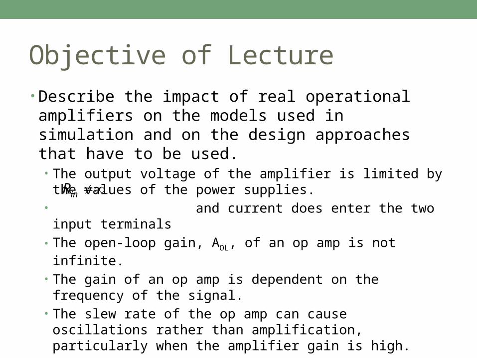
Inverting Amplifier: Voltage Supplies
is
if
V+ = 15VV– = -10V
i
i1 = 0
i2 = 0

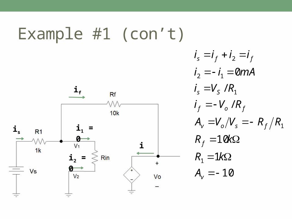
Example #1 (con’t)
i1 = 0
i2 = 0is
if
V+ = 15VV– = -10V
i
Example #1 (con’t)
i2 = 0
i1 = 0is
if
i
10
1
10
/
/
0
1
1
1
12
2
v
f
fsov
fof
Ss
ffs
A
kR
kR
RRVVA
RVi
RVi
mAii
iiii
Example #1 (con’t)
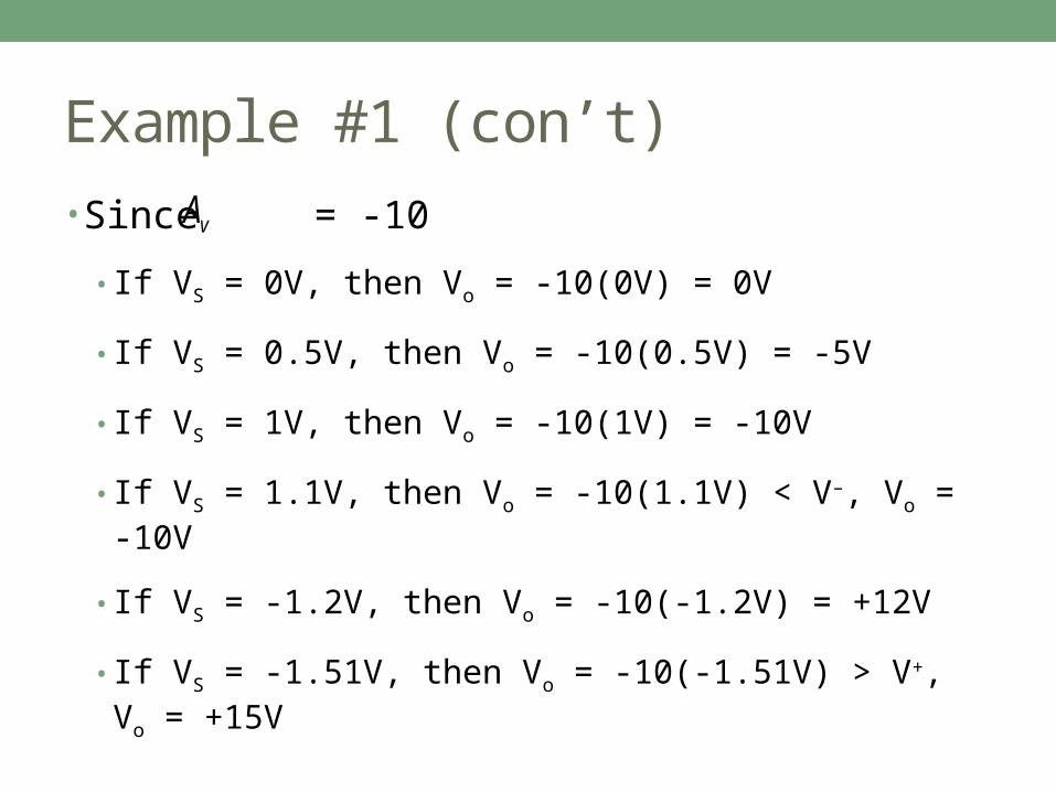
• Since = -10
• If VS = 0V, then Vo = -10(0V) = 0V
• If VS = 0.5V, then Vo = -10(0.5V) = -5V
• If VS = 1V, then Vo = -10(1V) = -10V
• If VS = 1.1V, then Vo = -10(1.1V) < V–, Vo = -10V
• If VS = -1.2V, then Vo = -10(-1.2V) = +12V
• If VS = -1.51V, then Vo = -10(-1.51V) > V+, Vo = +15V
vA

Example #1 (con’t)• Voltage transfer characteristic
Slope of the voltage transfer characteristic in the linear
region is equal to AV.

Rails• Rails is another turn for the voltage supplies that power
the operational amplifier.• Rail-to-rail operation means that the output voltage can equal V+
and V– at some points during its operation.
• 15 mV away from the voltage supplies is close enough to be called rail-to-rail.

http://www.ti.com/lit/ds/symlink/lm741.pdf
LM 741 Operational Amplifier

Non-symmetrical Swing• LM324 operational amplifier where VCCmax = 32 V

Inverting Amplifier: Finite Rin
is
if
i
is
if
i
i1 0
i2 0
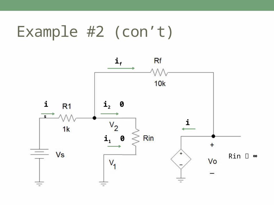
i1 0
i2 0is
if
i
Example #2 (con’t)
Rin ∞
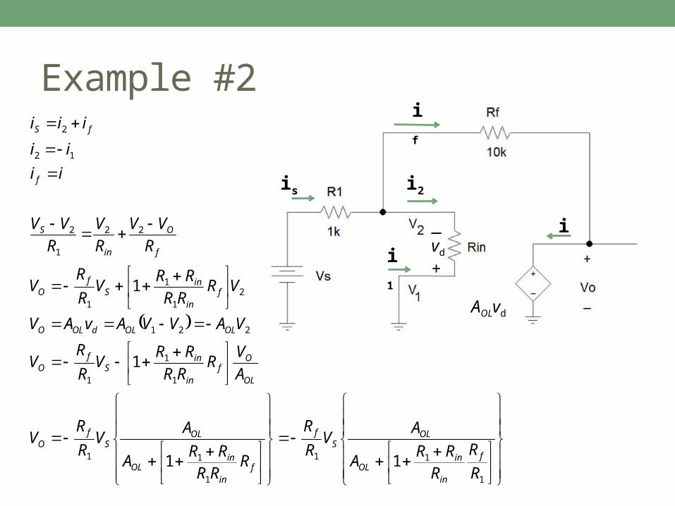
Example #2
1
11
1
11
1
1
1
221
21
1
1
22
1
2
12
2
11
1
1
R
R
RRR
A
AV
R
R
RRRRR
A
AV
R
RV
A
VR
RR
RRV
R
RV
VAVVAvAV
VRRR
RRV
R
RV
R
VV
R
V
R
VV
ii
ii
iii
f
in
inOL
OLS
f
fin
inOL
OLS
fO
OL
Of
in
inS
fO
OLOLdOLO
fin
inS
fO
f
O
in
S
f
fS
i1
i2is
if
i_vd
+
AOLvd
Gain
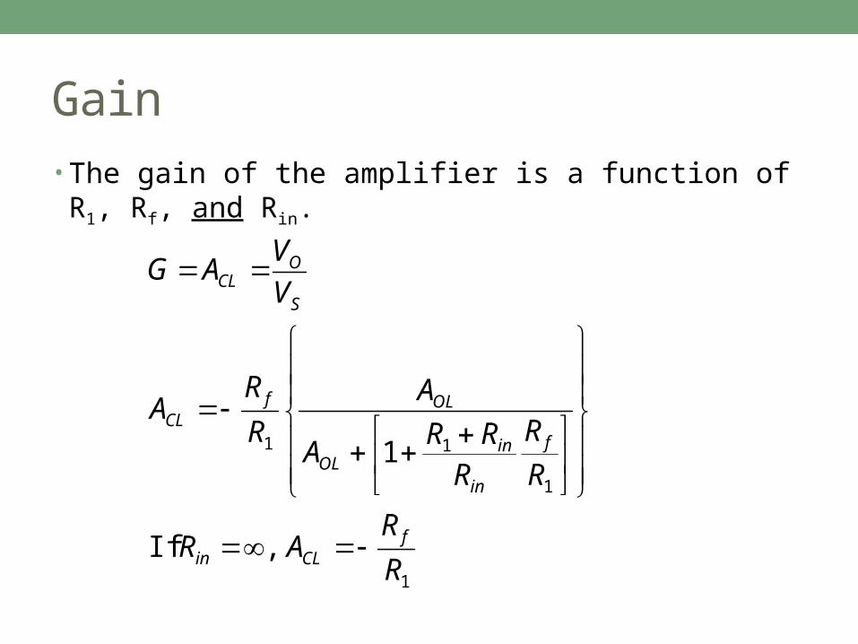
• The gain of the amplifier is a function of R1, Rf, and Rin.
1
1
11
, If
1
R
RAR
R
R
RRR
A
A
R
RA
V
VAG
fCLin
f
in
inOL
OLfCL
S
OCL

Differential Voltage (vd )
• Since Rin ∞, then i1 and i2 are not equal to zero.
• That means that the voltages at the input terminals of the op amp are not equal• V1 V2
• vd 0 V
• Because of nonideal operation of the transistors inside the operational amplifier, vd 0 V even when VO = 0 V.
• Thus, there is an input offset voltage V1 – V2 0V.
• Some transistors have a pin that allow you to counterbalance this offset voltage.
Gain
• As the open-loop gain, AOL, of the op amp is finite, the closed-loop gain is a function R1, Rf, Rin, and AOL.
OL
CL
in
inf
f
in
inOL
OLfCL
S
OCL
AG
GA
R
RR
R
R
R
R
RRR
A
A
R
RA
V
VAG
11
1
and GLet
1
1
1
1
11
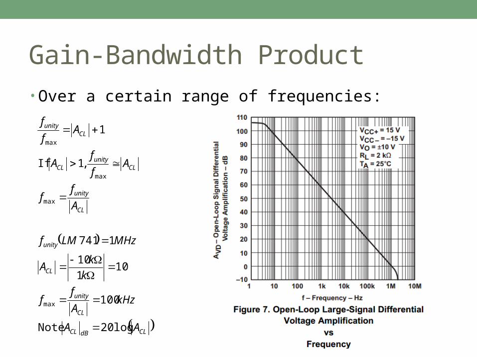
Gain-Bandwidth Product• Over a certain range of frequencies:
CLdBCL
CL
unity
CL
unity
CL
unity
CLunity
CL
CLunity
AA
kHzA
ff
k
kA
MHzLMf
A
ff
Af
fA
Af
f
log 20 Note
100
101
10
1741
,1 If
1
max
max
max
max

Slew Rate• The speed at which the output voltage changes after a change in the
input voltage.• When the closed-loop gain is very large and the operating frequency is
high, there is a chance that the output voltage will not follow the input voltage because it didn’t have time to reach the desired value before the input voltage changed.• When this happens, it is possible for the op amp circuit to start oscillating.
Electronic Design Project• The time-varying signal will be very small.
• To maximize the range of the mbed ADC that will be used to digitize the analogue signal, the amplifier will have to have a large gain.
• Because there will be significant noise on the signal that you want to detect, a bandpass filter will have to be designed that removes dc and very low frequency ac signals and removes high frequency noise.• Given the frequency range that the bandpass filter must operate
and that we would like the pulse meter to be powered by a battery, the resistors used in the filters will be large.

Op Amp Circuits to Consider• Buffers (Voltage Followers)
• Isolate one subsystem from another• Used in impedance matching
• Cascade Amplifiers• Several amplifiers in series where the overall gain is the
multiplication of the gain of each amplifier in series
• Active Filter• An op amp with a combination of resistors and capacitors at the
input termal and/or in the feedback loop.• This is considered to be a filter (low, high, or bandpass) with gain.• Passive filters (RC networks) are always lossy
• VO never is exactly equal to Vin

Op Amp Circuits to Consider (con’t)• Because there is only +9V, +5V, +3.3V, and ground
available (the battery, the voltage regulator output, and the logical high voltage on the mbed), inverting amplifiers should not be used because at least half of the signal will be lost.• Consider non-inverting amplifiers and difference amplifiers.