Embed Size (px)
Citation preview
Analog Integrated Circuits
Lecture 4: Differential Amplifiers
Analog Integrated Circuits
Lecture 4: Differential Amplifiers
ELC 601 – Fall 2013
Dr. Ahmed Nader
Dr. Mohamed M. Aboudina
Department of Electronics and Communications Engineering
Faculty of Engineering – Cairo University
11/8/2013
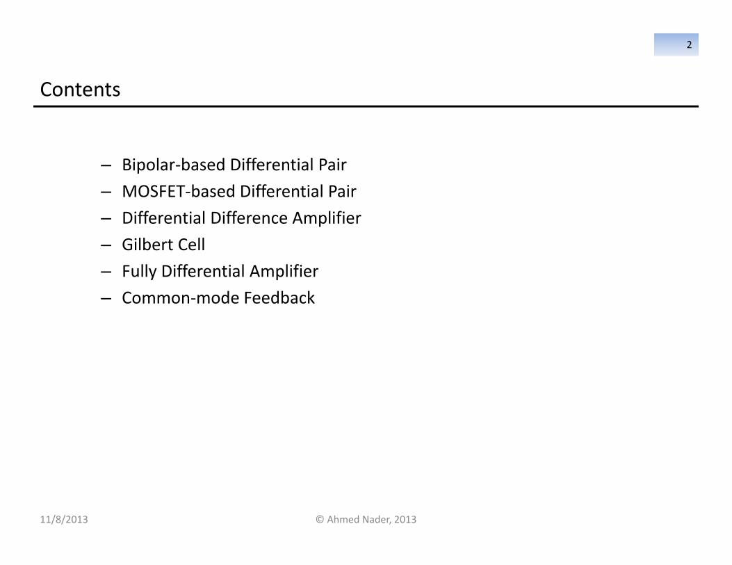
Contents
– Bipolar-based Differential Pair
– MOSFET-based Differential Pair
– Differential Difference Amplifier
– Gilbert Cell
– Fully Differential Amplifier
– Common-mode Feedback
© Ahmed Nader, 2013
2
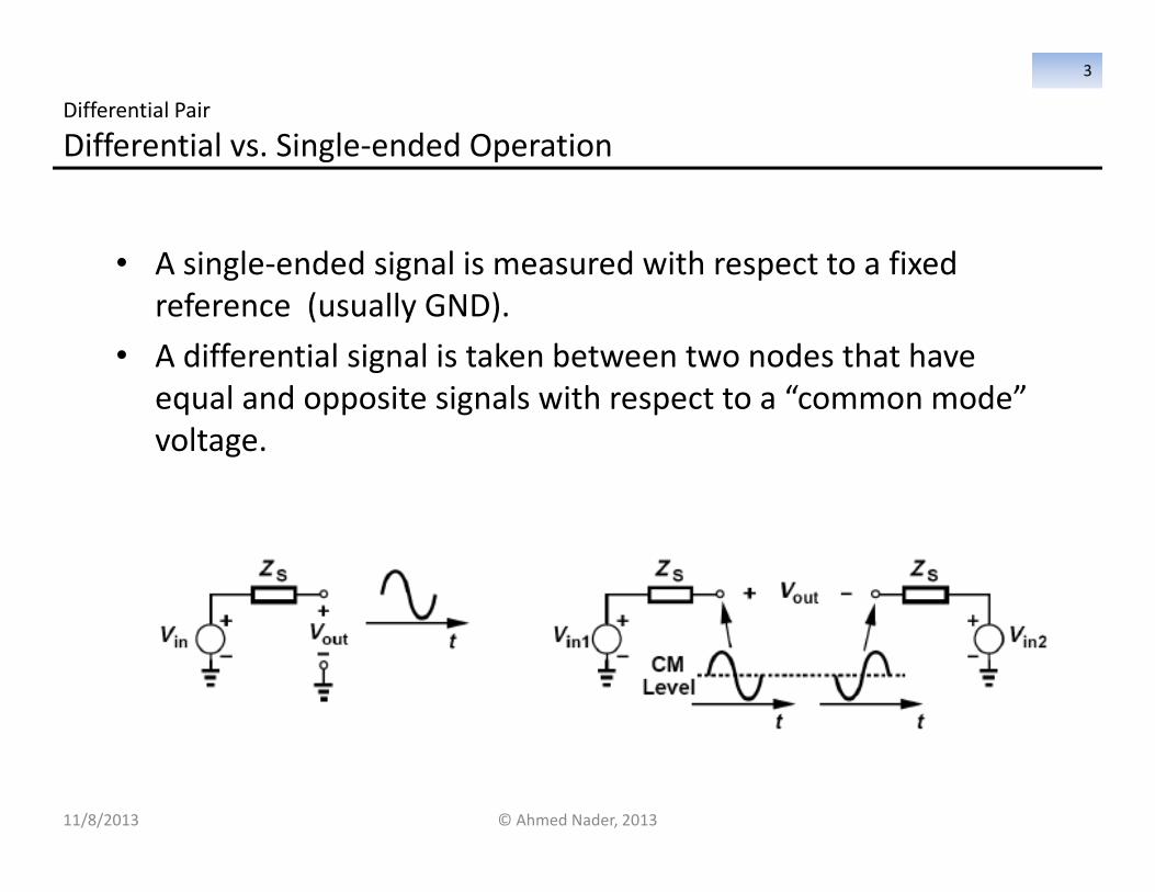
Differential Pair
Differential vs. Single-ended Operation
• A single-ended signal is measured with respect to a fixed
reference (usually GND).
• A differential signal is taken between two nodes that have
equal and opposite signals with respect to a “common mode”
voltage.
11/8/2013 © Ahmed Nader, 2013
3
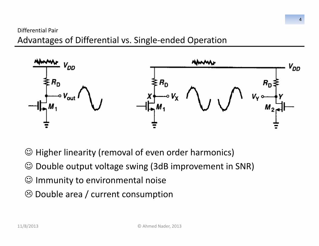
Differential Pair
Advantages of Differential vs. Single-ended Operation
11/8/2013
☺ Higher linearity (removal of even order harmonics)
☺ Double output voltage swing (3dB improvement in SNR)
☺ Immunity to environmental noise
� Double area / current consumption
© Ahmed Nader, 2013
4
Differential Pair
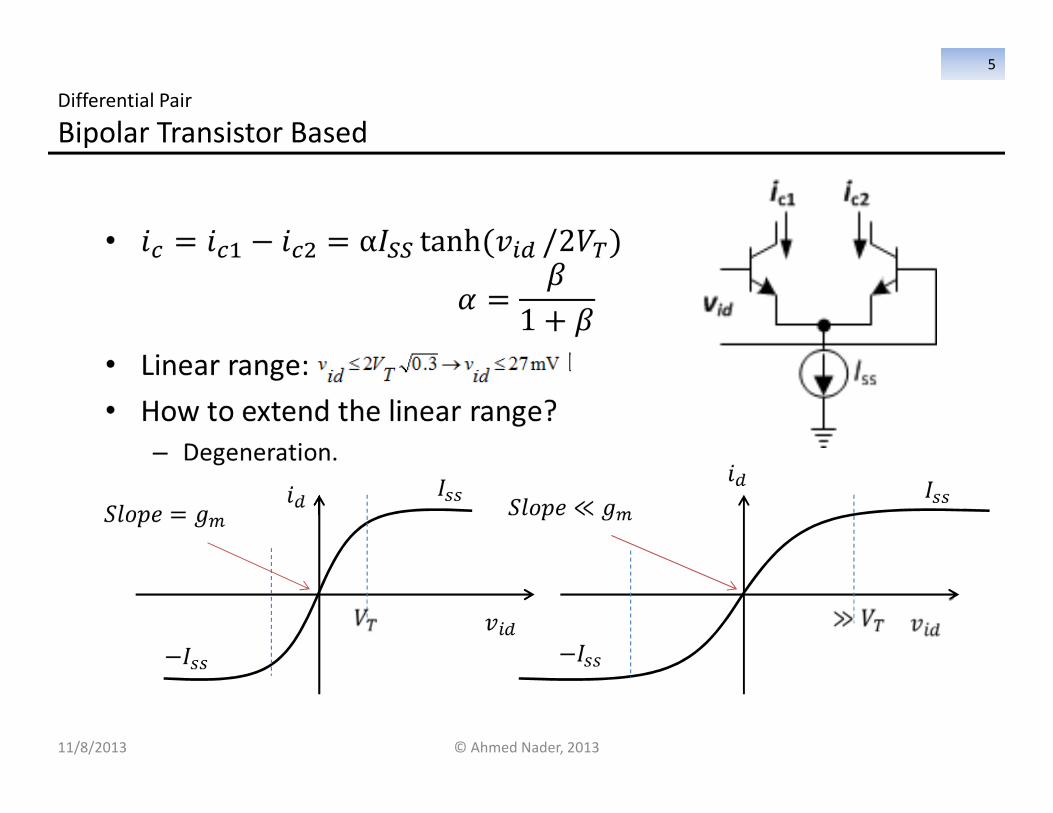
11/8/2013
Bipolar Transistor Based
© Ahmed Nader, 2013
5
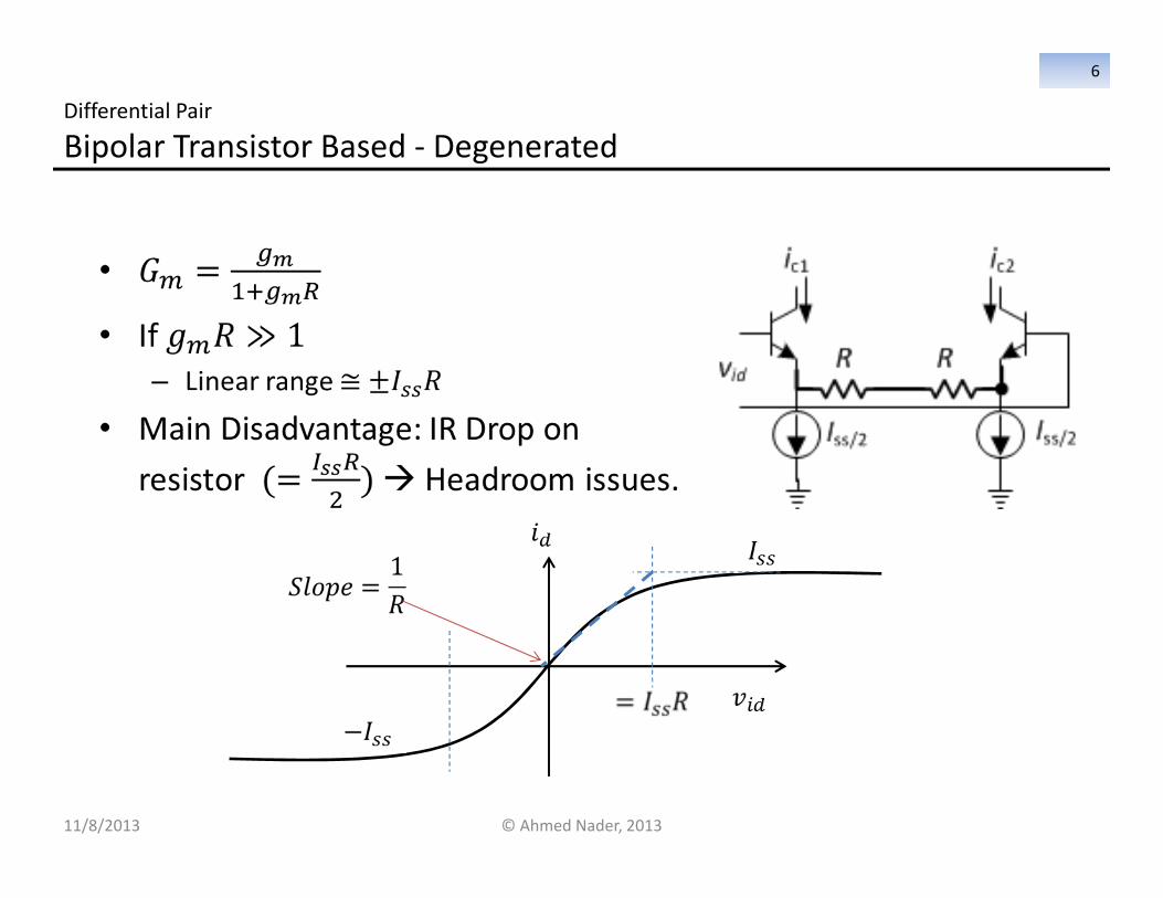
Differential Pair
11/8/2013
Bipolar Transistor Based - Degenerated
© Ahmed Nader, 2013
6
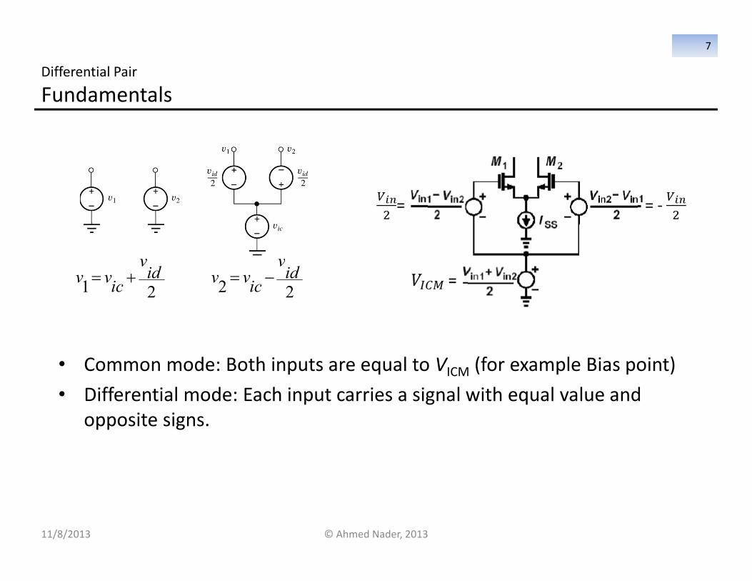
Differential Pair
Fundamentals
11/8/2013
21idv
icvv +=
22idv
icvv −=
© Ahmed Nader, 2013
7
• Common mode: Both inputs are equal to VICM (for example Bias point)
• Differential mode: Each input carries a signal with equal value and
opposite signs.
Differential Pair
Small-Signal Analysis
11/8/2013
Circuit analysis is done by
superposition of differential-mode
and common-mode signal portions.
21 ov
ov
odv −=
2
21 ov
ov
ocv+
=
=icvidv
ccAcdA
dcAddA
ocvodv
Add = differential-mode gain
Acd = common-mode to differential-mode
conversion gain
Acc = common-mode gain
Adc = differential mode to common-mode
conversion gain
For ideal symmetrical amplifier, Acd = Adc = 0.
Purely differential-mode input gives purely
differential-mode output and vice versa.
=∴icvidv
ccAddA
ocvodv 0
0
© Ahmed Nader, 2013
8
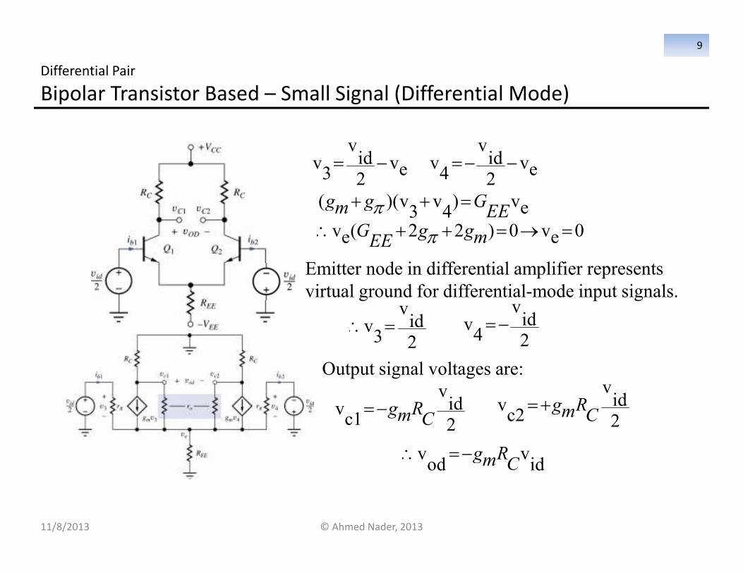
Differential Pair
11/8/2013
Bipolar Transistor Based – Small Signal (Differential Mode)
0ev0)22(ev
ev)4
v3
v)((
=→=++∴
=++
mggEEG
EEGgmg
π
π
2id
v
4v −=
ev2id
v
3v −= ev
2id
v
4v −−=
Output signal voltages are:
2id
v
c1v
CRmg−= 2
idv
c2v
CRmg+=
idv
odv
CRmg−=∴
2id
v
3v =∴
Emitter node in differential amplifier represents
virtual ground for differential-mode input signals.
© Ahmed Nader, 2013
9
Differential Pair
11/8/2013
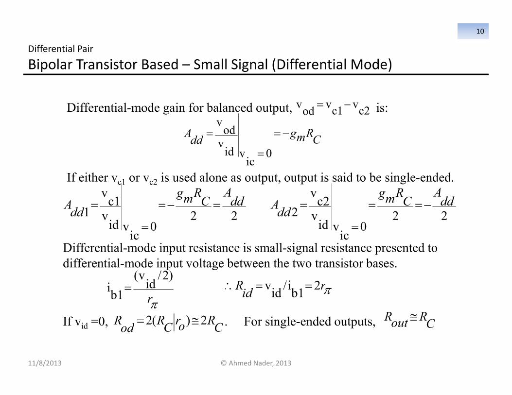
Bipolar Transistor Based – Small Signal (Differential Mode)
Differential-mode gain for balanced output, is:
If either vc1 or vc2 is used alone as output, output is said to be single-ended.
CRmgdd
A −=
=
=
0ic
vidvod
vc2
vc1
vod
v −=
220
icvid
vc1
v
1ddA
CRmg
ddA =−=
=
=22
0ic
vidvc2
v
2ddA
CRmg
ddA −==
=
=
Differential-mode input resistance is small-signal resistance presented to
differential-mode input voltage between the two transistor bases.
If vid =0, . For single-ended outputs,
πridR 2
b1i/
idv ==∴
CRorC
RodR 2)(2 ≅= R
out≅RC
πr
)2/id
v(
b1i =
© Ahmed Nader, 2013
10
Differential Pair
11/8/2013
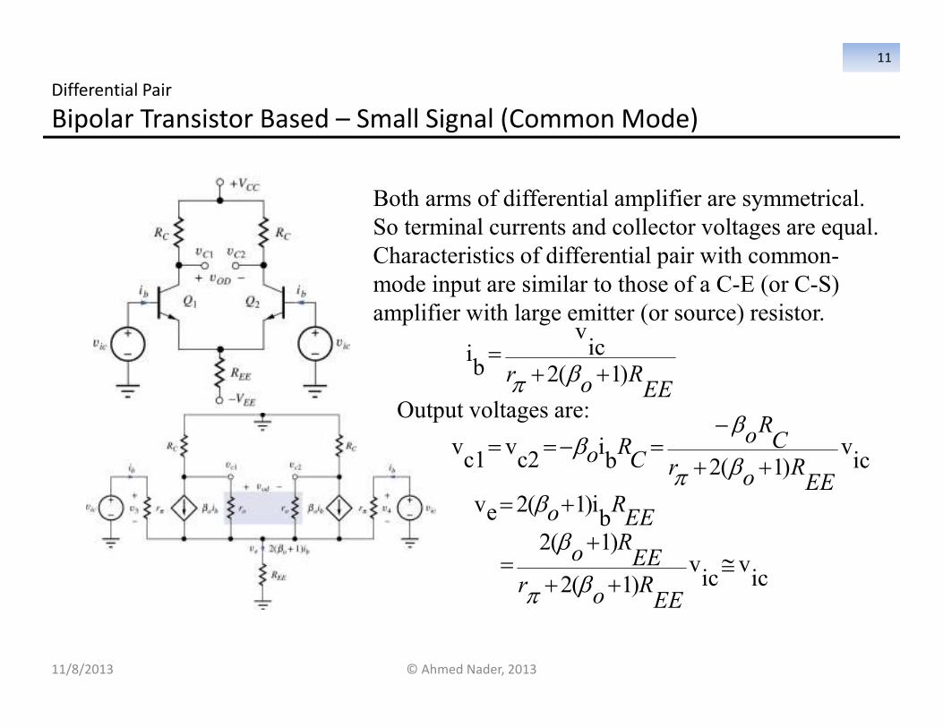
Bipolar Transistor Based – Small Signal (Common Mode)
Both arms of differential amplifier are symmetrical.
So terminal currents and collector voltages are equal.
Characteristics of differential pair with common-
mode input are similar to those of a C-E (or C-S)
amplifier with large emitter (or source) resistor.
Output voltages are:EERor )1(2
icv
bi
++=
βπ
icv
)1(2bi
c2v
c1v
EERor
CRo
CRo ++
−=−==
βπ
ββ
ve=2(βo+1)ibREE
=2(βo+1)R
EErπ +2(β
o+1)R
EE
vic≅v
ic
© Ahmed Nader, 2013
11
Differential Pair
11/8/2013
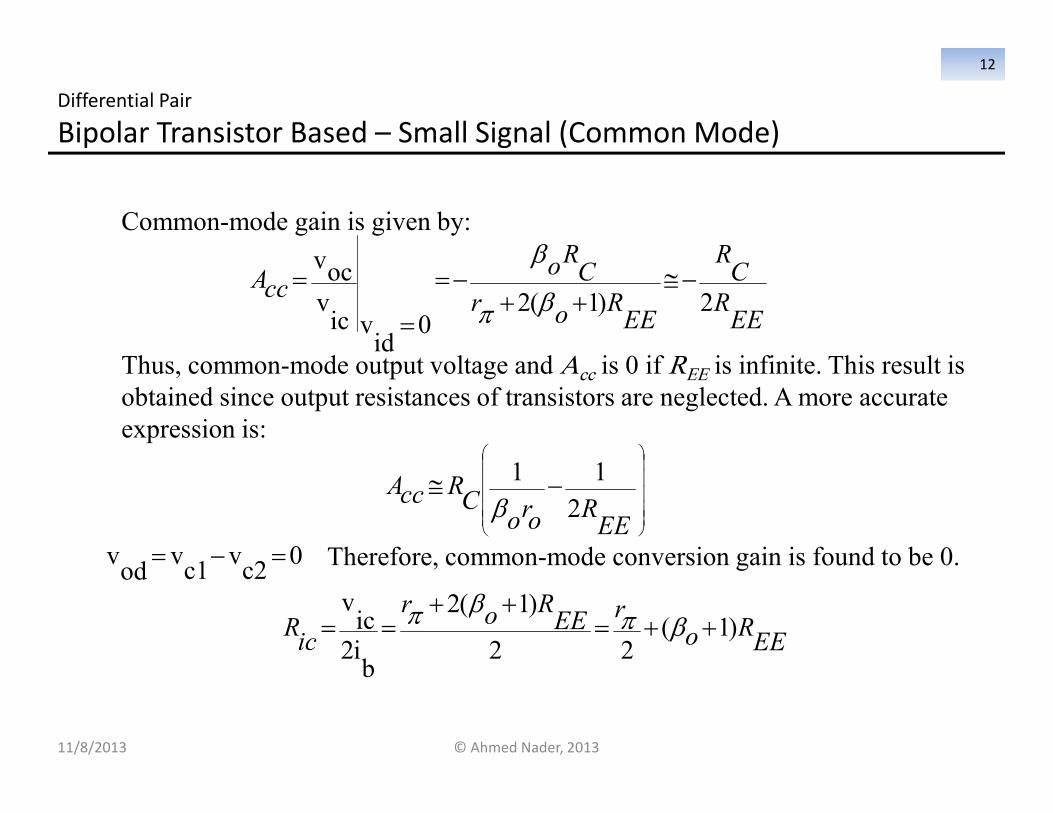
Bipolar Transistor Based – Small Signal (Common Mode)
Common-mode gain is given by:
Thus, common-mode output voltage and Acc is 0 if REE is infinite. This result is
obtained since output resistances of transistors are neglected. A more accurate
expression is:
Therefore, common-mode conversion gain is found to be 0.
EER
CR
EERor
CRo
ccA2)1(2
0id
vicv
ocv
−≅++
−=
=
=βπ
β
0c2
vc1
vod
v =−=
−≅
EERoro
CRccA
2
11
β
EERo
rEERor
icR )1(
22
)1(2
bi2ic
v++=
++== βπ
βπ
© Ahmed Nader, 2013
12
Differential Pair
11/8/2013
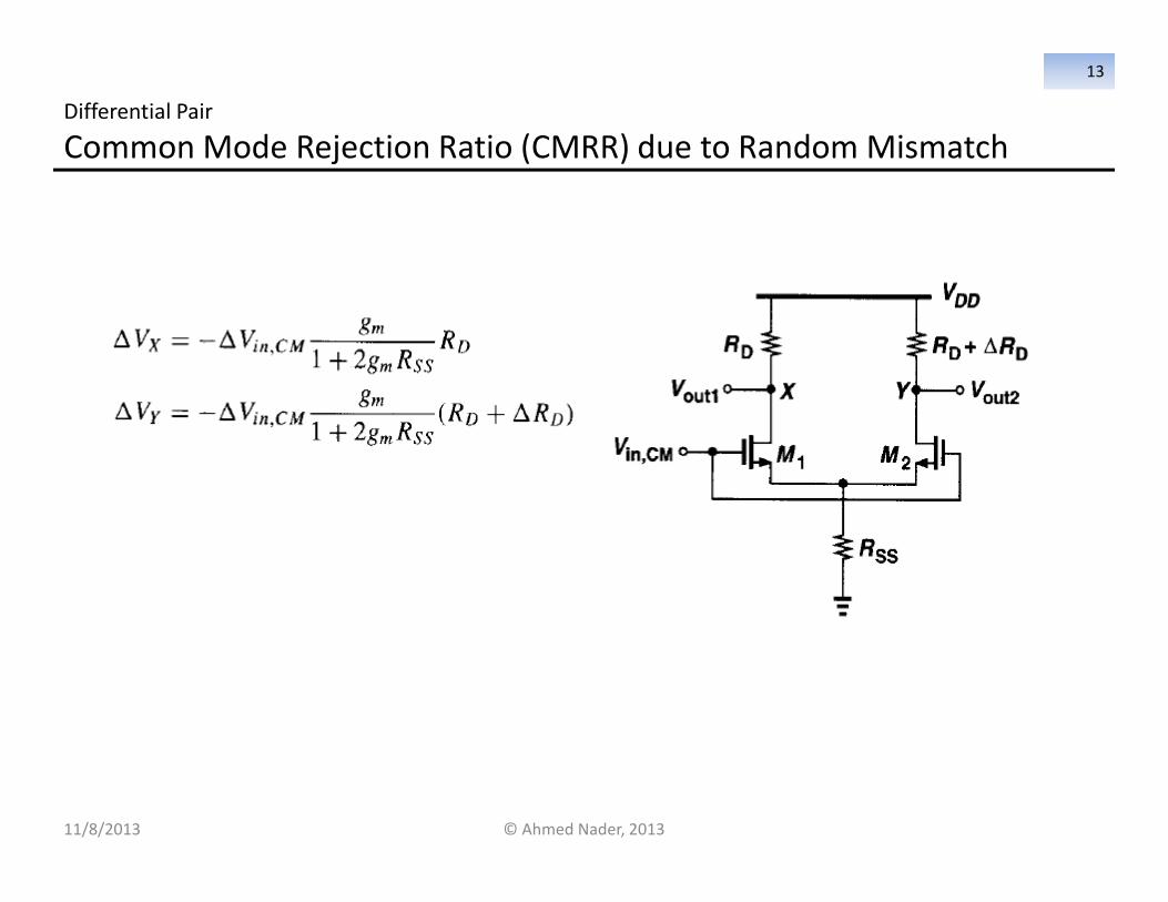
Common Mode Rejection Ratio (CMRR) due to Random Mismatch
© Ahmed Nader, 2013
13
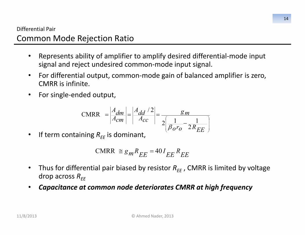
Differential Pair
11/8/2013
Common Mode Rejection Ratio
• Represents ability of amplifier to amplify desired differential-mode input signal and reject undesired common-mode input signal.
• For differential output, common-mode gain of balanced amplifier is zero, CMRR is infinite.
• For single-ended output,
• If term containing REE is dominant,
• Thus for differential pair biased by resistor REE , CMRR is limited by voltage drop across REE
• Capacitance at common node deteriorates CMRR at high frequency
−===
EERoro
mg
ccAddA
cmAdmA
2112
2/CMRR
β
EER
EEI
EERmg 40CMRR =≅
© Ahmed Nader, 2013
14
Differential Pair
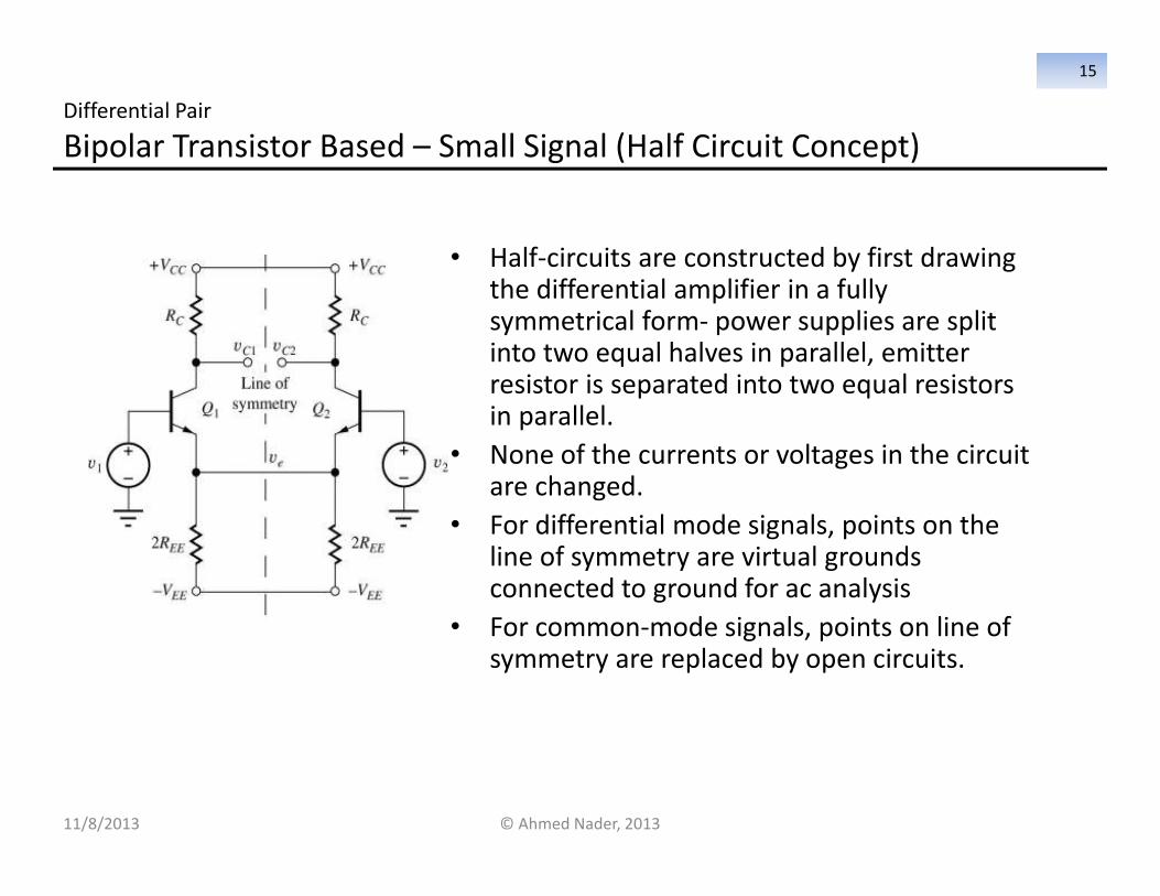
11/8/2013
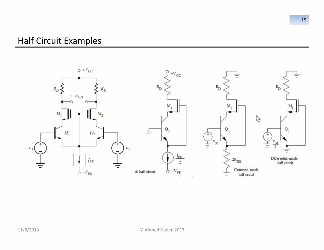
Bipolar Transistor Based – Small Signal (Half Circuit Concept)
• Half-circuits are constructed by first drawing the differential amplifier in a fully symmetrical form- power supplies are split into two equal halves in parallel, emitter resistor is separated into two equal resistors in parallel.
• None of the currents or voltages in the circuit are changed.
• For differential mode signals, points on the line of symmetry are virtual grounds connected to ground for ac analysis
• For common-mode signals, points on line of symmetry are replaced by open circuits.
© Ahmed Nader, 2013
15

Differential Pair
11/8/2013
Bipolar Transistor Based – Small Signal (Half Circuit Concept)
• Half-circuits are constructed by first drawing the differential amplifier in a fully symmetrical form- power supplies are split into two equal halves in parallel, emitter resistor is separated into two equal resistors in parallel.
• None of the currents or voltages in the circuit are changed.
• For differential mode signals, points on the line of symmetry are virtual grounds connected to ground for ac analysis
• For common-mode signals, points on line of symmetry are replaced by open circuits.
© Ahmed Nader, 2013
16
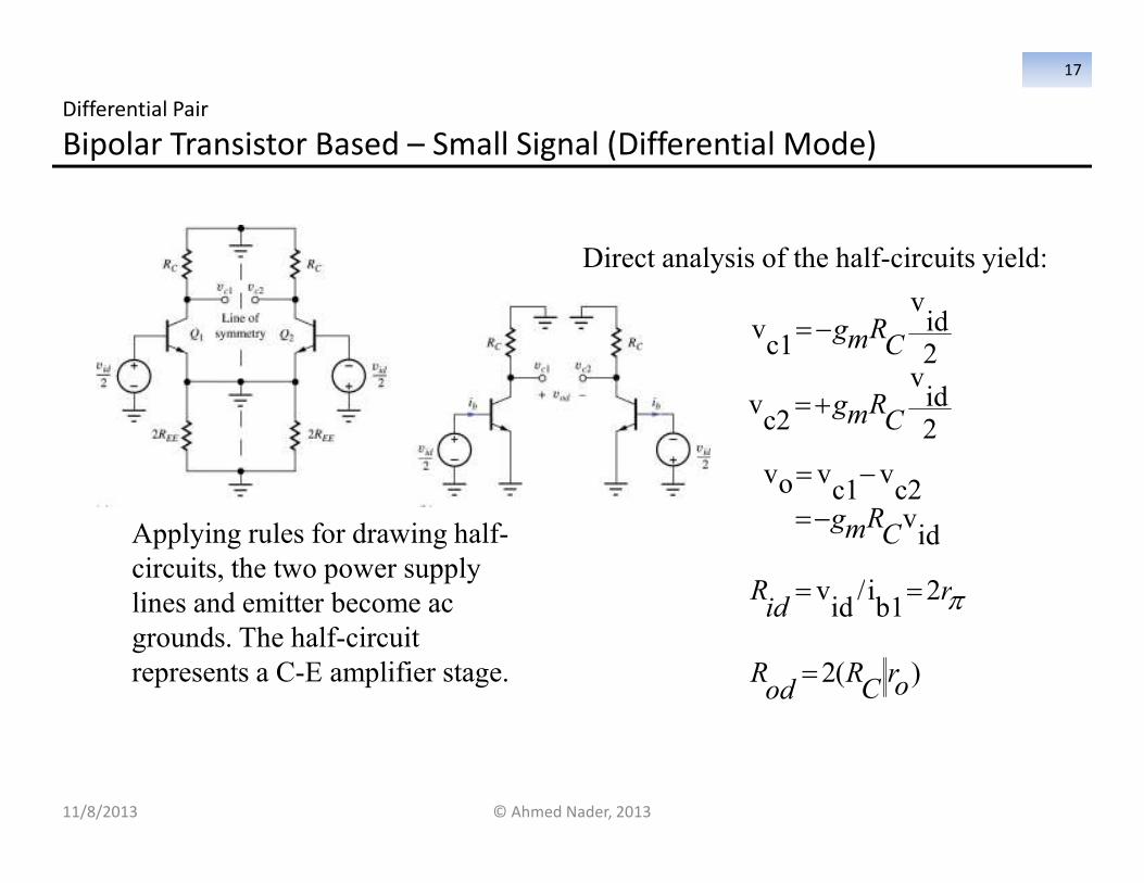
Differential Pair
11/8/2013
Bipolar Transistor Based – Small Signal (Differential Mode)
Applying rules for drawing half-
circuits, the two power supply
lines and emitter become ac
grounds. The half-circuit
represents a C-E amplifier stage.
2id
v
c1v
CRmg−=
2id
v
c2v
CRmg+=
vo= vc1−v
c2 =−gmRCv
id
Direct analysis of the half-circuits yield:
πridR 2
b1i/
idv ==
)(2 orCR
odR =
© Ahmed Nader, 2013
17
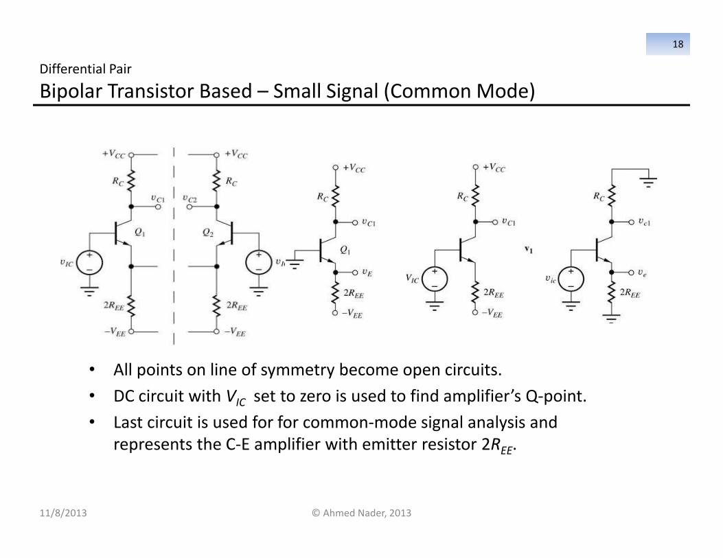
Differential Pair
11/8/2013
Bipolar Transistor Based – Small Signal (Common Mode)
• All points on line of symmetry become open circuits.
• DC circuit with VIC set to zero is used to find amplifier’s Q-point.
• Last circuit is used for for common-mode signal analysis and
represents the C-E amplifier with emitter resistor 2REE.
© Ahmed Nader, 2013
18
11/8/2013 © Ahmed Nader, 2013
19
Half Circuit Examples
11/8/2013 © Ahmed Nader, 2013
20
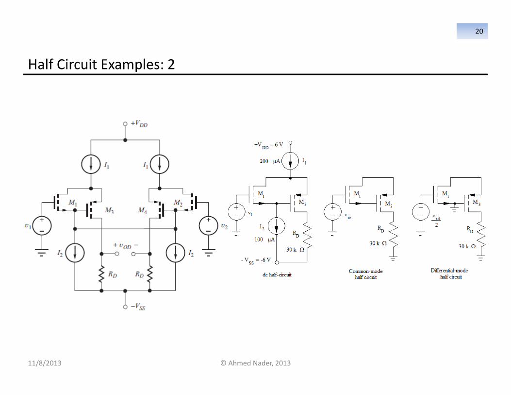
Half Circuit Examples: 2
11/8/2013 © Ahmed Nader, 2013
21
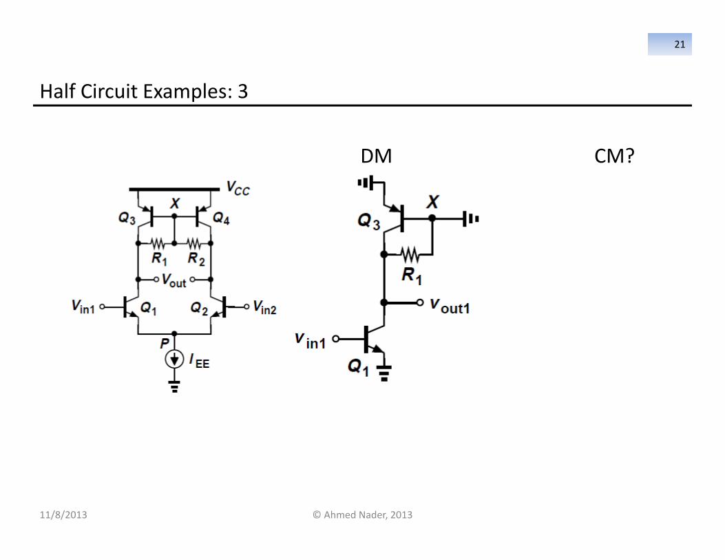
Half Circuit Examples: 3
DM CM?
Differential Pair
11/8/2013
MOSFET-Based
© Ahmed Nader, 2013
22
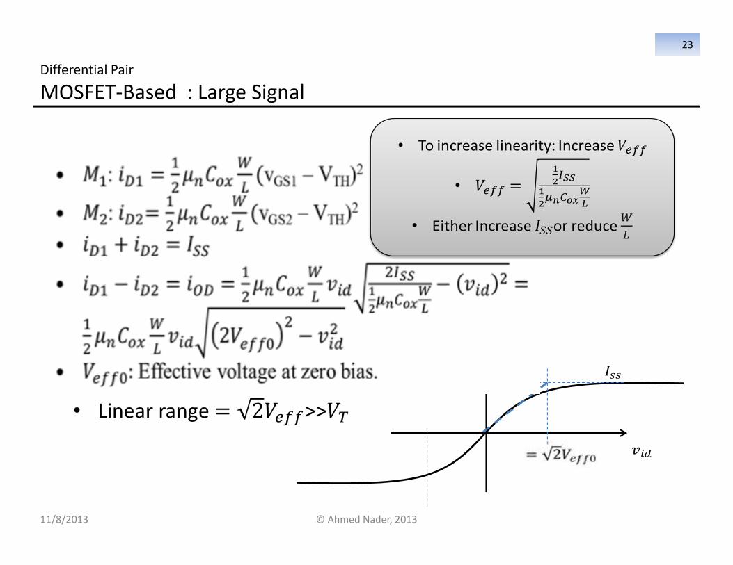
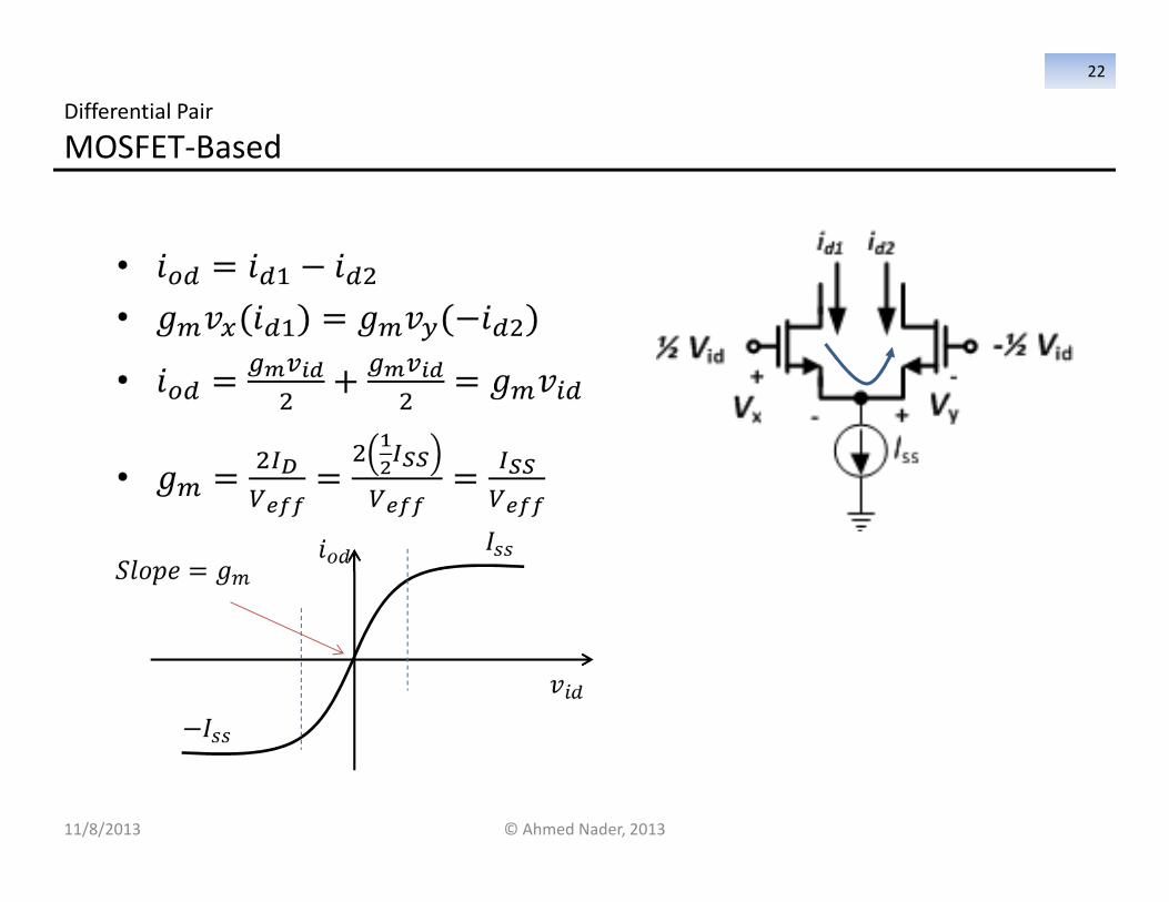
Differential Pair
11/8/2013
MOSFET-Based : Large Signal
© Ahmed Nader, 2013
23
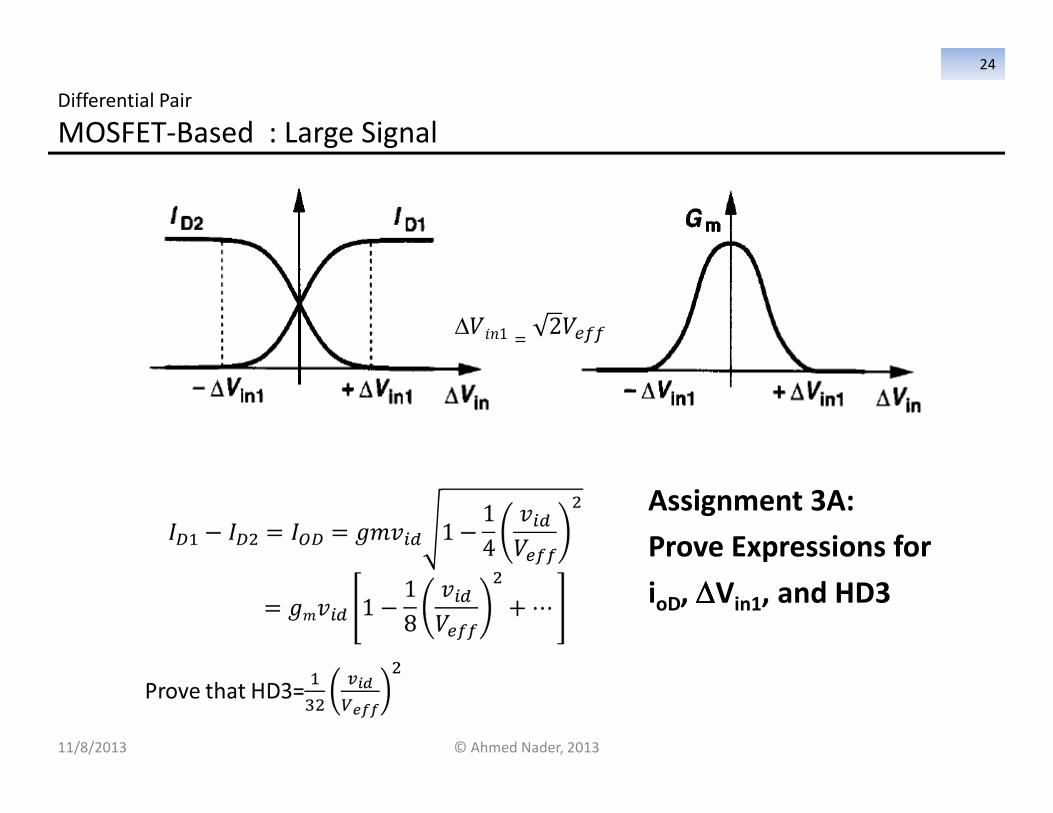
Differential Pair
11/8/2013
MOSFET-Based : Large Signal
Assignment 3A:
Prove Expressions for
ioD, ∆∆∆∆Vin1, and HD3
© Ahmed Nader, 2013
24
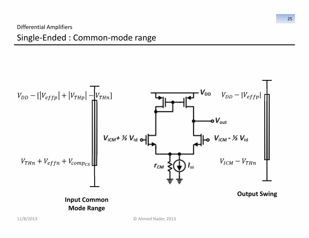
Differential Amplifiers
11/8/2013
Single-Ended : Common-mode range
Input Common
Mode Range
Output Swing
© Ahmed Nader, 2013
25
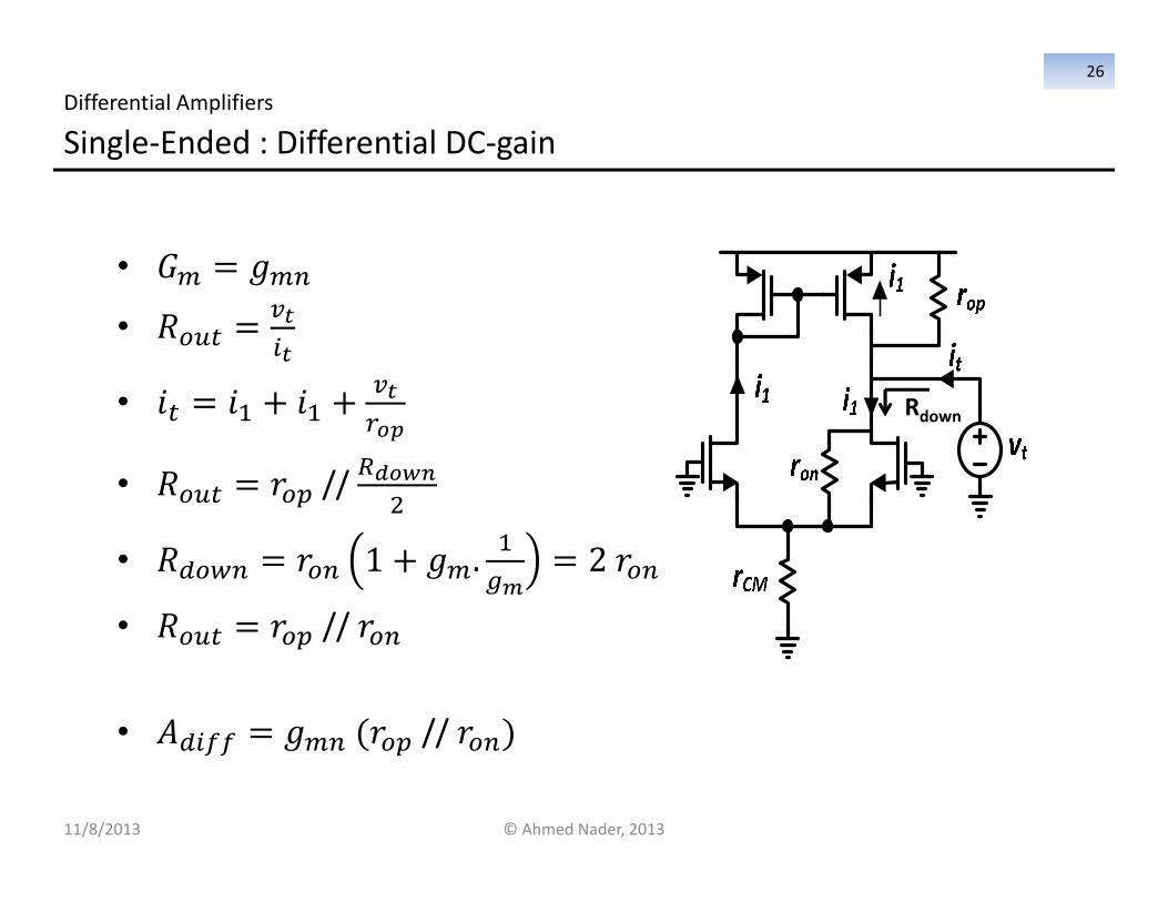
Differential Amplifiers
11/8/2013
Single-Ended : Differential DC-gain
© Ahmed Nader, 2013
26
• �� = ���
• ��� =�
��
• = � + � +�
���
• ��� = ��� // �����
�
• ����� = ��� 1 + ��.�
� = 2 ���
• ��� = ��� // ���
• "��## = ��� (��� // ���)
Rdown
Differential Amplifiers
11/8/2013
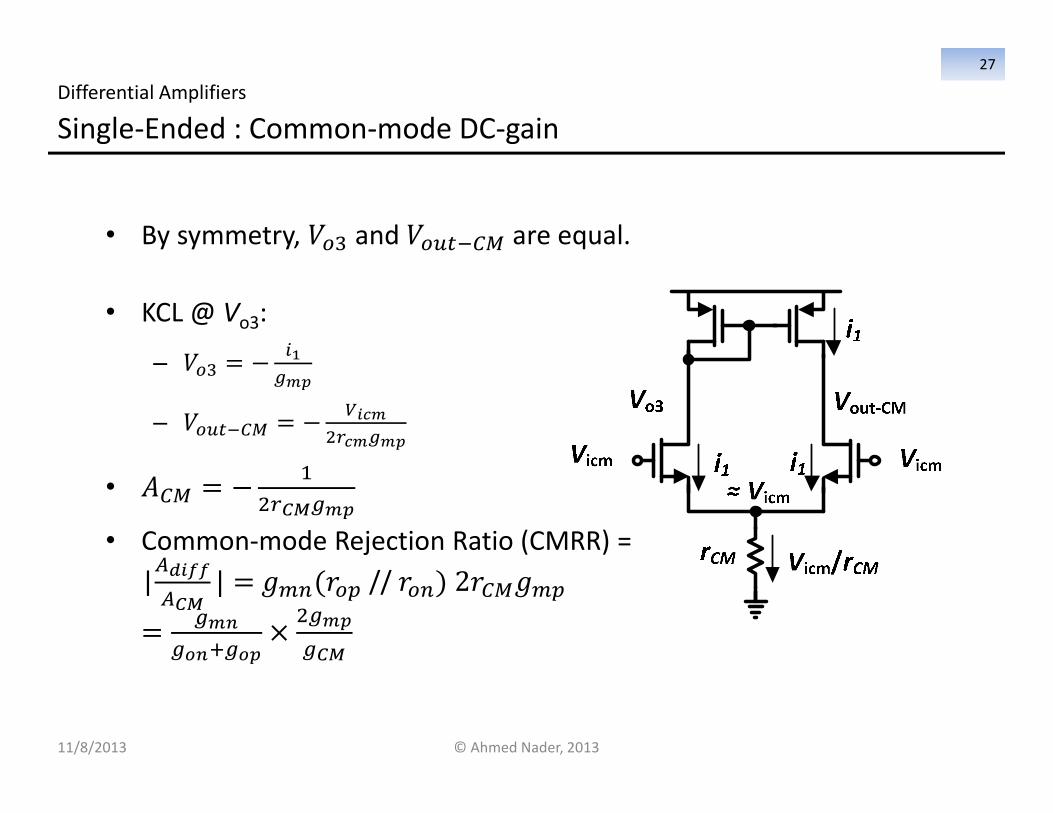
Single-Ended : Common-mode DC-gain
© Ahmed Nader, 2013
27
• By symmetry, &�' and &��()* are equal.
• KCL @ Vo3:
– &�' = −�,
� �
– &��()* = −-./
��/ � �
• ")* = −�
��01� �
• Common-mode Rejection Ratio (CMRR) =
|2�.33
201| = ���(��� // ���) 2�)*���
=� �
���5���×
�� �
�01
11/8/2013
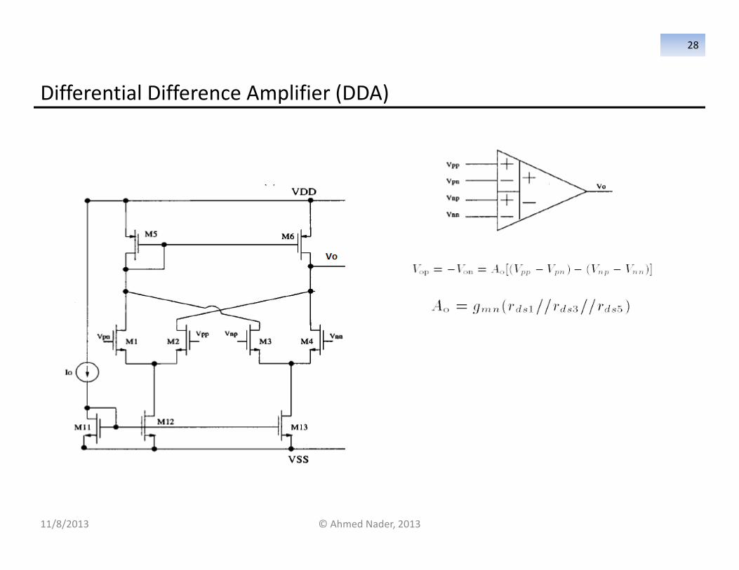
Differential Difference Amplifier (DDA)
© Ahmed Nader, 2013
28
11/8/2013
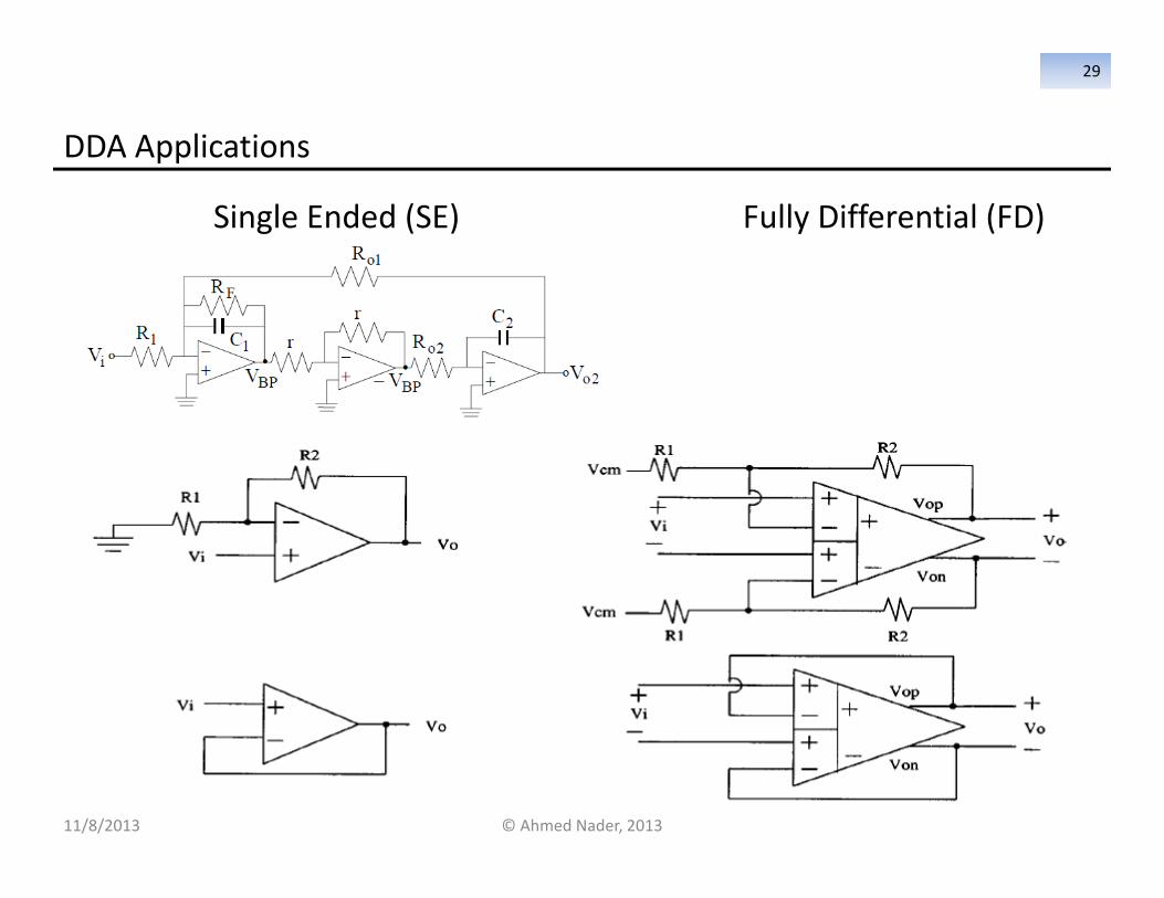
DDA Applications
© Ahmed Nader, 2013
29
Single Ended (SE) Fully Differential (FD)
11/8/2013
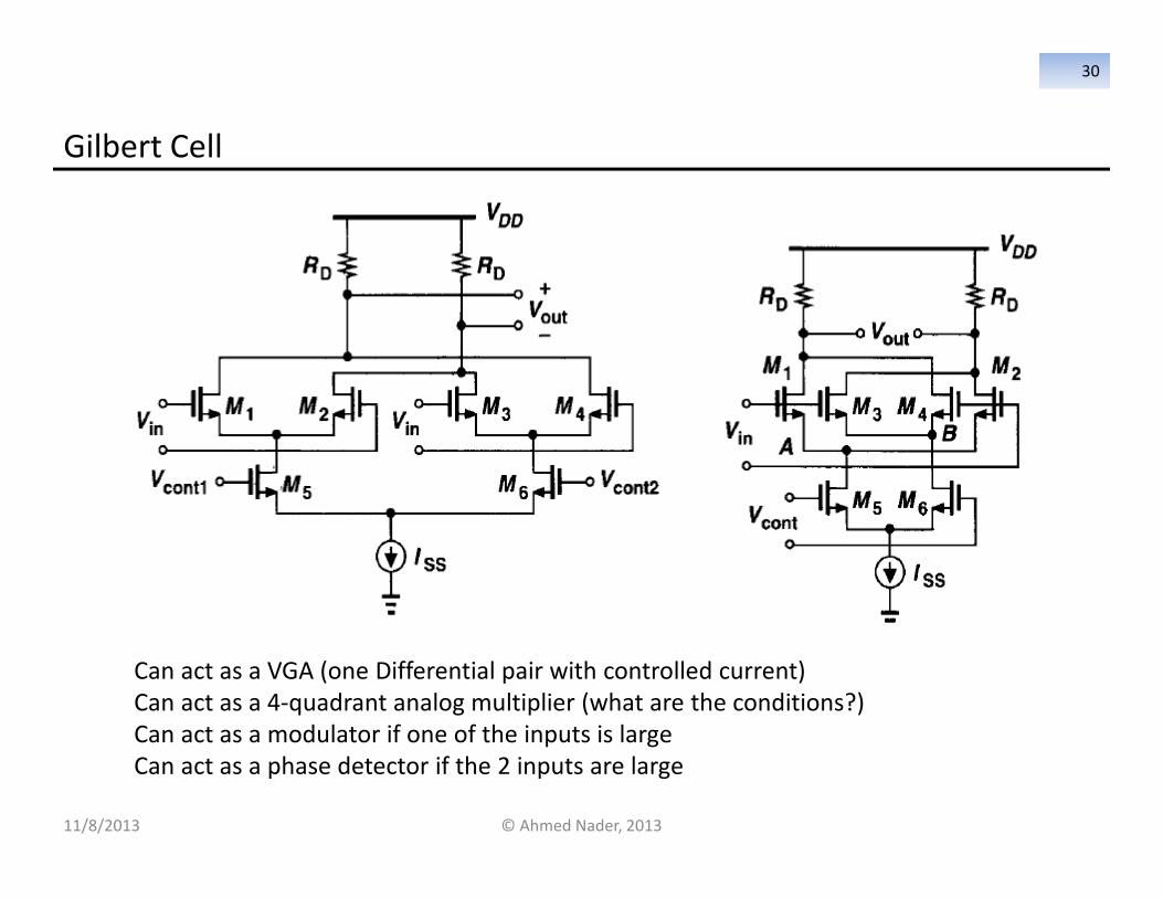
Gilbert Cell
Can act as a VGA (one Differential pair with controlled current)
Can act as a 4-quadrant analog multiplier (what are the conditions?)
Can act as a modulator if one of the inputs is large
Can act as a phase detector if the 2 inputs are large
© Ahmed Nader, 2013
30
11/8/2013
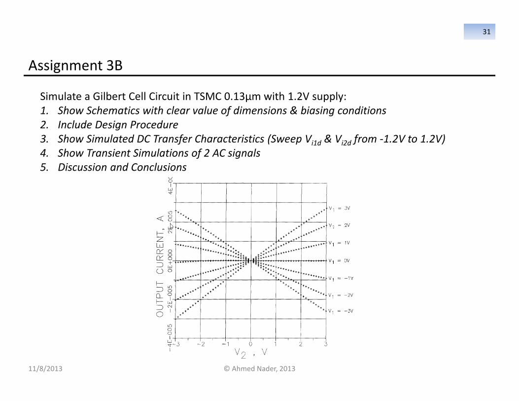
Assignment 3B
Simulate a Gilbert Cell Circuit in TSMC 0.13µm with 1.2V supply:
1. Show Schematics with clear value of dimensions & biasing conditions
2. Include Design Procedure
3. Show Simulated DC Transfer Characteristics (Sweep Vi1d & Vi2d from -1.2V to 1.2V)
4. Show Transient Simulations of 2 AC signals
5. Discussion and Conclusions
© Ahmed Nader, 2013
31
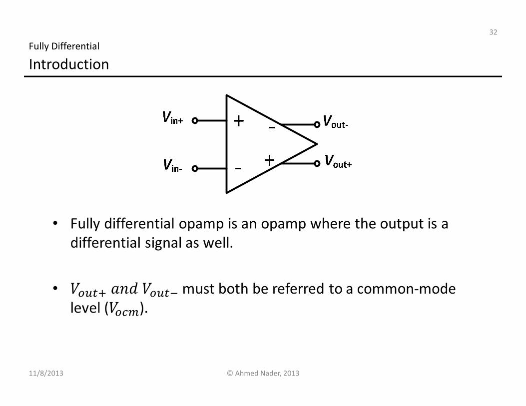
Fully Differential
11/8/2013 © Ahmed Nader, 2013
32
Introduction
Fully Differential
11/8/2013 © Ahmed Nader, 2013
33
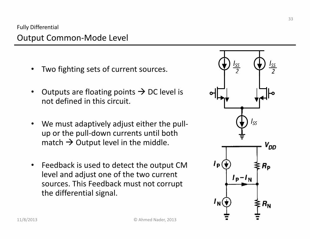
Output Common-Mode Level
• Two fighting sets of current sources.
• Outputs are floating points � DC level is not defined in this circuit.
• We must adaptively adjust either the pull-up or the pull-down currents until both match � Output level in the middle.
• Feedback is used to detect the output CM level and adjust one of the two current sources. This Feedback must not corrupt the differential signal.
Fully Differential
11/8/2013 © Ahmed Nader, 2013
34
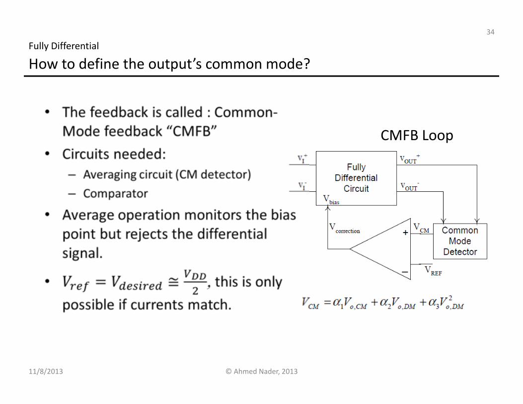
How to define the output’s common mode?
CMFB Loop
Fully Differential
11/8/2013 © Ahmed Nader, 2013
35
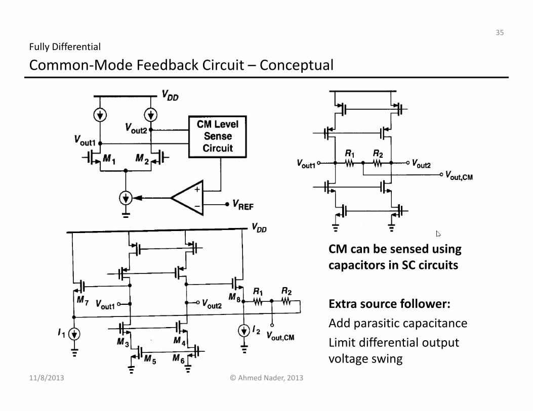
Common-Mode Feedback Circuit – Conceptual
CM can be sensed using
capacitors in SC circuits
Extra source follower:
Add parasitic capacitance
Limit differential output
voltage swing
Fully Differential
11/8/2013 © Ahmed Nader, 2013
36
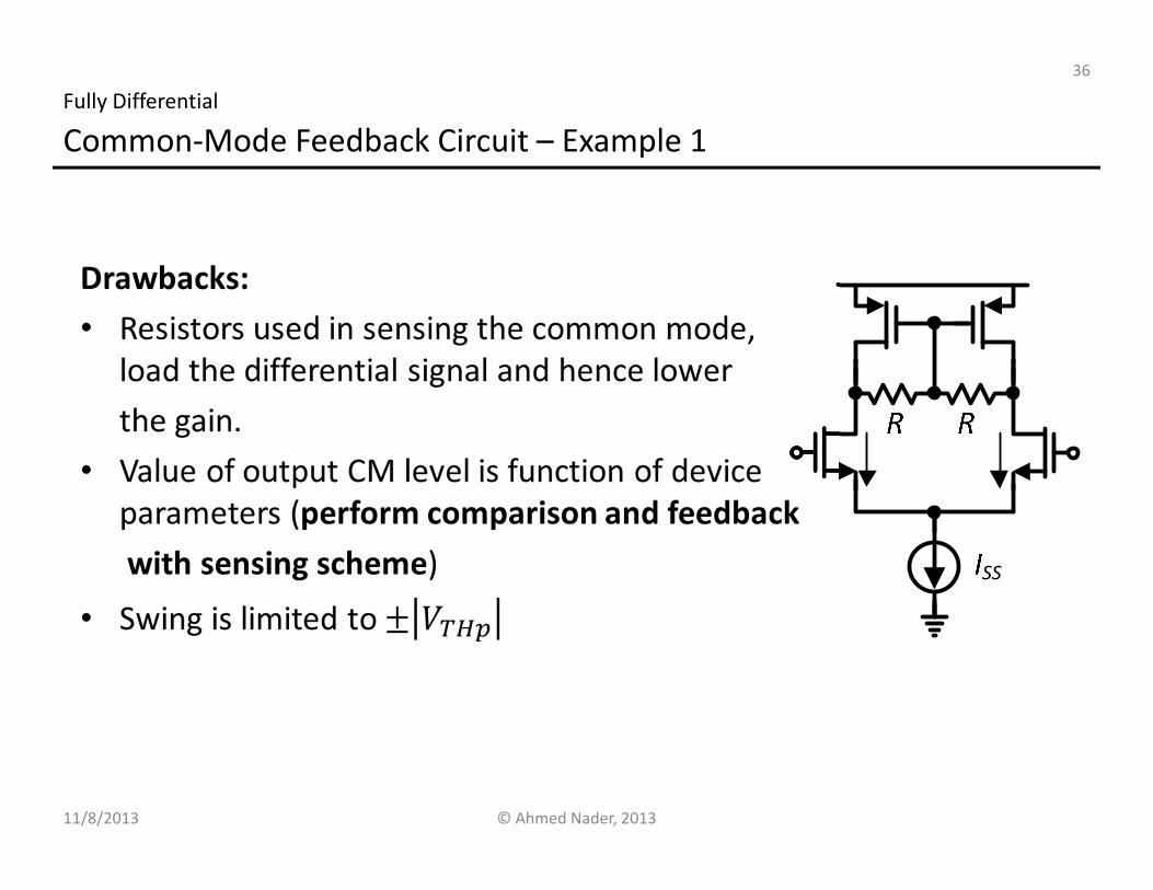
Common-Mode Feedback Circuit – Example 1
SS
Fully Differential
11/8/2013 © Ahmed Nader, 2013
37
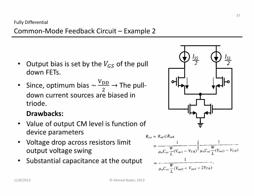
Common-Mode Feedback Circuit – Example 2
Fully Differential
11/8/2013 © Ahmed Nader, 2013
38
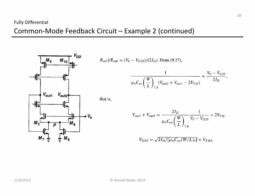
Common-Mode Feedback Circuit – Example 2 (continued)
Fully Differential
11/8/2013 © Ahmed Nader, 2013
39
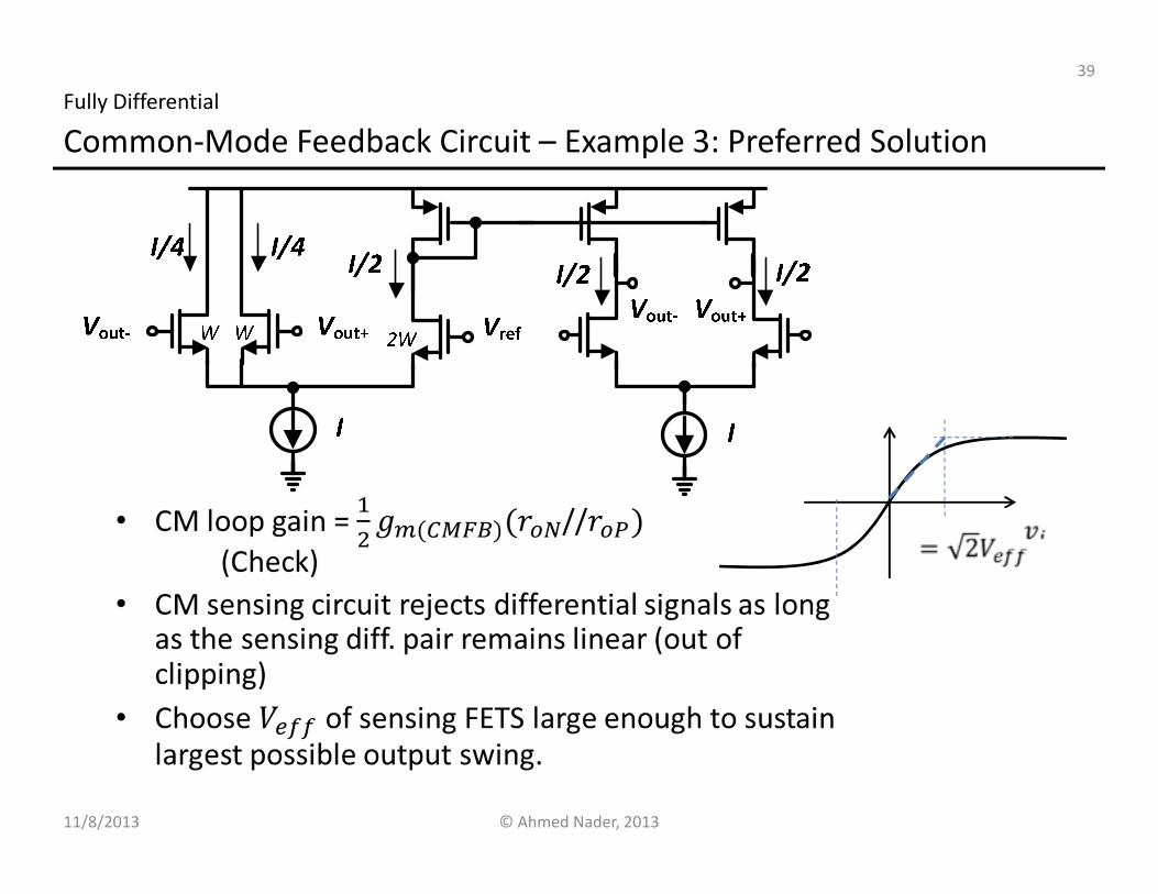
Common-Mode Feedback Circuit – Example 3: Preferred Solution
Fully Differential
11/8/2013 © Ahmed Nader, 2013
40
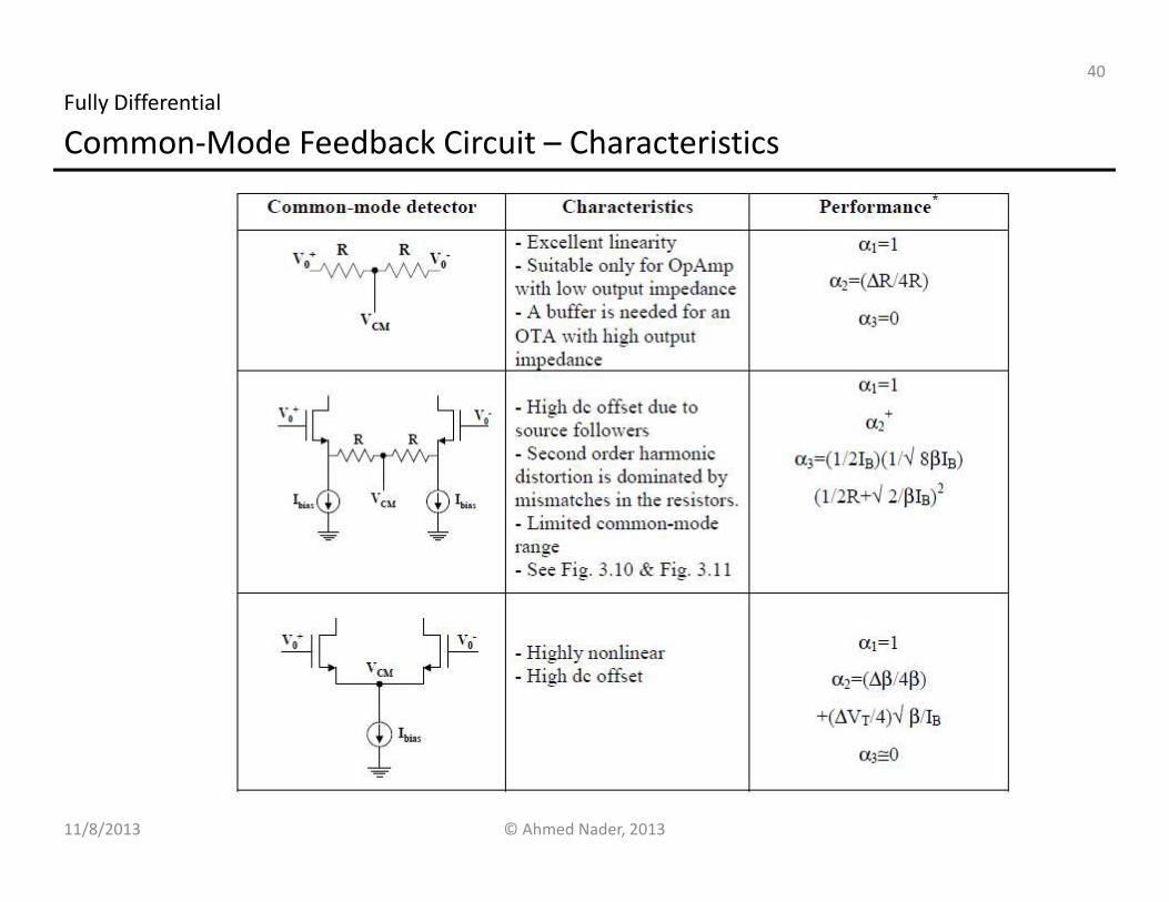
Common-Mode Feedback Circuit – Characteristics
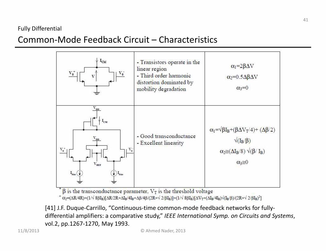
Fully Differential
11/8/2013 © Ahmed Nader, 2013
41
Common-Mode Feedback Circuit – Characteristics
[41] J.F. Duque-Carrillo, “Continuous-time common-mode feedback networks for fully-
differential amplifiers: a comparative study,” IEEE International Symp. on Circuits and Systems,
vol.2, pp.1267-1270, May 1993.