Embed Size (px)
Citation preview
OPEN
ORIGINAL ARTICLE
Nonlinear terahertz devices utilizing semiconductingplasmonic metamaterials
Huseyin R Seren1, Jingdi Zhang2,3, George R Keiser2,4, Scott J Maddox5, Xiaoguang Zhao1, Kebin Fan1,Seth R Bank5, Xin Zhang1 and Richard D Averitt2,3
The development of responsive metamaterials has enabled the realization of compact tunable photonic devices capable of
manipulating the amplitude, polarization, wave vector and frequency of light. Integration of semiconductors into the active
regions of metallic resonators is a proven approach for creating nonlinear metamaterials through optoelectronic control of the
semiconductor carrier density. Metal-free subwavelength resonant semiconductor structures offer an alternative approach to cre-
ate dynamic metamaterials. We present InAs plasmonic disk arrays as a viable resonant metamaterial at terahertz frequencies.
Importantly, InAs plasmonic disks exhibit a strong nonlinear response arising from electric field-induced intervalley scattering,
resulting in a reduced carrier mobility thereby damping the plasmonic response. We demonstrate nonlinear perfect absorbers
configured as either optical limiters or saturable absorbers, including flexible nonlinear absorbers achieved by transferring the
disks to polyimide films. Nonlinear plasmonic metamaterials show potential for use in ultrafast terahertz (THz) optics and for
passive protection of sensitive electromagnetic devices.
Light: Science & Applications (2016) 5, e16078; doi:10.1038/lsa.2016.78; published online 20 May 2016
Keywords: nonlinear absorbers; nonlinear metamaterials; plasmonic semiconductor metamaterials; terahertz metamaterials;transfer printing
INTRODUCTION
The advent of active and tunable metamaterials (MMs) introduced anew path toward controlling light-matter interactions with thepossibility to impact photonic applications spanning from microwaveto visible frequencies1. Nonlinear MMs represent an important class ofactive electromagnetic composites that can potentially pave the way toproduce tailored nonlinear optical phenomena such as harmonicgeneration or self-focusing2. Pioneering prominent examples of non-linear MMs have been demonstrated in the microwave region wherenonlinear lumped circuit elements were used3. At infrared frequencies,field enhancement plasmonic MMs provide an important routetoward creating enhanced nonlinear composites4–7.Optically responsive materials at terahertz (THz) frequencies have
also been demonstrated in the past decade through judicious MMdesign8–10. This includes the creation of dynamically tunable MMdevices employing optical, mechanical or electrical controlmethods1,11–15. Nonlinear THz MMs have also beendemonstrated16–20. The majority of tunable and nonlinear THz MMshave incorporated semiconductors into the active region of split ringresonators to enable dynamic tuning of the electromagneticresponse13,14,21,22. It is also possible to exclusively employ semiconduc-tors to create plasmonic devices at THz and infrared frequencies23–25.The plasma frequency of semiconductors can be tuned by adjusting the
doping level, providing a path toward THz plasmonic semiconductorMMs (PSMM)26–29. The response of PSMM can be tailored viastructure and geometry and can be modulated using, as examples,electric, magnetic and thermal stimuli. Importantly, semiconductorsexhibit large nonlinearities at THz frequencies30–36 enabling (asdemonstrated below) nonlinear plasmonics and providing a keycapability for future terahertz circuits and systems6,37.We have created PSMMs using n-doped InAs (n-InAs) thin films
patterned into disk arrays that are resonant at THz frequencies. As iswell known, the plasmonic response of a particle arises from dielectricconfinement. This results in a resonant response that is determined bythe geometry and the carrier concentration with the quality of theresonance determined by the scattering rate or, in the case ofsemiconducting plasmonic particles, the mobility. Thus, n-InAs is anattractive plasmonic material at THz frequencies because of the highmobility (~20× 103 cm2 V−1 s− 1) and ability to control the resonancefrequency through doping. Further, as we demonstrate, InAs disksexhibit a strong nonlinear response. In particular, high-field terahertznonlinear transmission measurements reveal that the disk plasmonresonance exhibits a nonlinear response arising from field-inducedintervalley scattering of conduction band electrons to a low-mobilitysatellite valley. We utilized these nonlinear PSMMs to create bothsaturable absorbers (SAs) and optical limiters (OLs) by incorporating a
1Laboratory for Microsystems Technology, Department of Mechanical Engineering, Boston University, Boston, MA 02215, USA; 2Department of Physics, Boston University,Boston, MA 02215, USA; 3Department of Physics, UC San Diego, La Jolla, CA 92093, USA; 4School of Engineering, Brown University, Providence, RI 02912, USA and5Microelectronics Research Center, The University of Texas at Austin, Austin, TX 78758, USACorrespondence: X Zhang, Email: [email protected]; RD Averitt, Email: [email protected] 21 September 2015; revised 21 January 2016; accepted 25 January 2016; accepted article preview online 26 January 2016
Light: Science & Applications (2016) 5, e16078; doi:10.1038/lsa.2016.78& 2016 CIOMP. All rights reserved 2047-7538/16www.nature.com/lsa
ground plane to create a perfect absorber geometry including flexibleabsorbers created via transfer of the InAs arrays to polyimide.
MATERIALS AND METHODS
FabricationFor our studies, 2-μm-thick n-InAs films were grown via molecularbeam epitaxy (MBE) with a Si doping concentration of 1017 cm− 3 ona 500-μm-thick semi-insulating (SI) GaAs substrate. A 100-nm-thickTi mask layer was patterned on the film using a lift-off technique.Next, an InAs film on a 1× 1 cm2 die was etched thoroughly usingreactive ion etching with a gas mixture of H2, CH4 and Ar. The Timask was then etched away in HF solution. For the perfect absorberson GaAs substrates, this procedure was followed by polyimide spincoating and curing, and 150 nm gold evaporation.To fabricate flexible absorbers with no substrate, we used a transfer
patterning technique. Thin films of 2-μm-thick n-doped InAs weregrown by MBE on a 500 nm AlAsSb sacrificial layer on semi-insulatingGaAs substrate. Subsequent to growth, the InAs film was patternedand etched into disks with a hexagonal symmetry (D= 60 μm,P= 72.7 μm), using a citric acid/H2O2 solution down. The exposedarea of the sacrificial layer was then etched away using a 5% HFsolution; at this step, the InAs disks remained attached to the GaAssubstrate by unexposed AlAsSb. Next, polyimide was spin-cast andcured, and Cr/Au/Ti layers were deposited on the polyimide as a dual-purpose ground plane and etchmask. Subsequently, 28 μm diameteretch holes were formed by RIE of the polyimide layer and wet etchingof the InAs, resulting in the disks acquired a ring shape. To completethe transfer of the InAs rings to polyimide, the AlAsSb sacrificial layerunderneath the InAs rings was etched away in a 5% HF bath. After 2 hof etching, the polyimide was peeled off from the GaAs substrate.A final citric acid dip was made to remove compound residues fromthe surface. Due to anisotropic wet etching of InAs, the fabricatedrings possessed a long axis diameter of 64 μm and a short axisdiameter of 60 μm. An explanatory figure showing fabrication steps forflexible PSMMs can be seen in Supplementary Fig. S1.
THz-TDSThe THz-time-domain spectroscopy (TDS) setup makes use of thetilted-pulse-front technique to generate THz pulses from a LiNbO3
crystal (see Supplementary Fig. S2). The THz pulses used in thisexperiment were ~ 1 ps in duration with a maximum electric fieldstrength of ~ 300 kV cm− 1. The field strength incident on the sampleis controlled through a pair of linear polarizers. Example time-domain
measurements of the PSMM and SI-GaAs reference are presented inSupplementary Fig. S3.
SimulationsIn our simulations, we used the Drude response for n-InAs with thefollowing parameters: Nd= 1e17 cm− 3, ε∞= 12.25, meff= 0.023, andμ= 3.5e3–1.9e4 cm2 V−1 s− 1. The SI-GaAs substrate is assumed tohave a relative dielectric constant of 12.94 with a frequency indepen-dent loss tangent of 0.006. A unit cell and a reference sample weresimulated in the time domain and the results were obtained in thesame manner as in the experiments (for example, by Fouriertransforming the time-domain data and performing a Fresnel analysisin the frequency domain). To include nonlinearities caused byintervalley scattering, we used a variable mobility and effective massin our Drude model of InAs. By varying the relationship betweenmobility and effective mass, we were able to account for the field-dependent collision frequency. Supplementary Tables S1 and S2 in theSupplementary Information provide the mobilities and effectivemasses used to model each nonlinear device.
RESULTS AND DISCUSSION
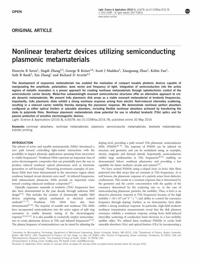
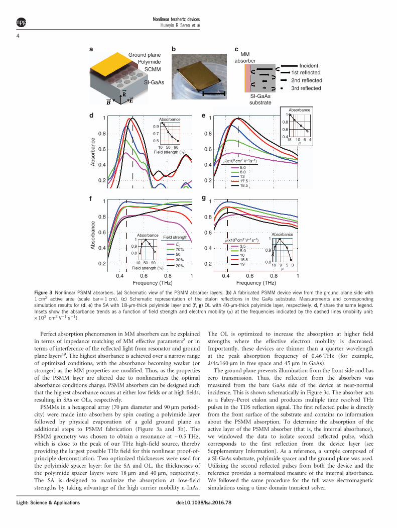
A PSMM composed of 70-μm-diameter n-InAs disks with 100 μmhexagonal lattice periodicity was fabricated as shown in Figure 1a and1b. The geometry was formed by dry etching of a 2-μm-thick n-InAsfilm grown on SI-GaAs using MBE38. Our samples were dopedto 1017 cm− 3, as shown in Figure 2, to obtain a strong plasmonicresponse at ~ 0.8 THz. The band structure, depicted in Figure 1c playsan important role in the plasmonic response. At low electric fields, thefree electrons reside predominantly in the Γ-valley and exhibit a smalleffective mass and high mobility. The oscillator strength of theplasmon resonance can, in principle, be modified at high electricfields through intervalley scattering or impact ionization30–35
(Figure 1c). For example, efficient intervalley scattering (Γ→L) wouldresult in a damping of the plasmon resonance because of theconsiderably larger effective mass and reduced mobility of carriers inthe L-valley.High-field THz-TDS was employed to characterize the samples
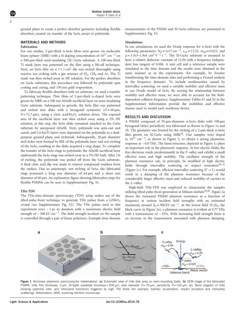
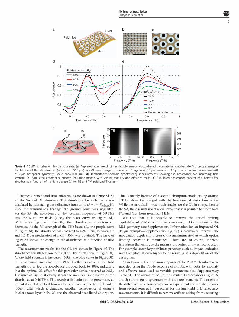
utilizing tilted-pulse-front generation in lithium niobate39,40. Figure 2ashows the measured PSMM plasmon resonance as a function offrequency at various incident field strengths with an estimatedmaximum around E0≈ 300 kV cm− 1. At the lowest field (0.1E0, theblack curve in Figure 2a), a plasmon resonance is evident at 0.77 THzwith a transmission of ~ 35%. With increasing field strength there isan increase in the transmission associated with plasmon damping.
Energy
<111><100>
L-valleymeff = 0.29
Γ-valleymeff = 0.023
X-valleymeff =0.64
Valence bandWave vector
a b c
n-InAs
SI-GaAs
SI-GaAs
n-InAs
P =100 μm
D = 70 μm
B
k
E
Figure 1 Nonlinear plasmonic semiconductor metamaterial. (a) Schematic view of InAs disk array on semi-insulating GaAs. (b) SEM image of the fabricatedPSMM: InAs film thickness: 2 μm, SI-GaAs substrate thickness=500 μm, disk diameter D=70 μm, periodicity P=100 μm. (c), Band diagram of InAsshowing potential inter- and intra-band transitions triggered by high THz fields (for example, ballistic acceleration, impact ionization and intervalleyscattering). Abbreviation: SEM, scanning electron microscope.
Nonlinear terahertz devicesHuseyin R Seren et al
2
Light: Science & Applications doi:10.1038/lsa.2016.78
At the highest field strength (E0, the purple curve in Figure 2a) thetransmission has increased to ~75%, an increase of 40% incomparison to the low-field case. Figure 2c shows the correspondingphase as a function of frequency (relative to the phase at the highestfield strength). The largest phase shift (between the lowest and highestfields) at ~ 0.9 THz was 35°; at 1.2 THz (well above resonance) it hasdecreased to ~22°. The observed damping is consistent with THzelectric field-induced intervalley scattering (Γ→L), resulting in adecrease in the average electron mobility41.To gain insight into the nonlinear response of the InAs disks, we
modeled the PSMMs using CST Microwave Studio (Framingham,MA, USA) utilizing the Drude model to describe the electromagneticresponse of InAs (see Supplementary Information for details). Inagreement with experiment, the simulated resonant response at~ 0.77 THz corresponds to the dipolar plasmonic mode of the diskstructure. To simulate the increased carrier scattering, we decreasedthe electron mobility, which results in a quenching of the plasmonoscillator strength in agreement with experiment (Figure 2b). Thisinterpretation is consistent with intervalley scattering, leading tocoexisting populations of electrons in the Γ and L valleys, whichyields an average effective mobility as indicated in Figure 2d.Specifically, our simulations are consistent with a decrease in theeffective mobility from 19× 103 cm2 V−1 s− 1 to 3.5 × 103 cm2 V−1 s− 1
on increasing the field from 0.1E0 to E0. Ignoring effects due tononparabolicity, impact ionization, and scattering to the X-valley, andassuming the Γ and L-valleys have constant mobilities of 20× 103 and20 cm2 V−1 s− 1, respectively, the observed change is consistent withgreater than 50% of the carriers being transferred to the L-valley. Inthe experimental data, there is also a slight shift in the resonancefrequency; we attribute this shift to the decrease in the plasmafrequency caused by an increase in effective mass arising from bandnonparabolicity and transfer to the L-valley at high fields42. This effectis well-captured in the simulations by increasing the effective electronmass (meff= 0.023→ 0.035) in the Drude model.The ability to fabricate MMs from semiconductor resonators opens
up vast opportunities for creating nonlinear active devices. In thefollowing, we demonstrate nonlinear absorbers (that is, SAs and OLs).Similar devices operating in the infrared currently find practical use inultrafast optics, mode locking and sensor/eye protection43,44. Indeed,bulk semiconductors can show a nonlinear absorption of THz lightdue to several electronic nonlinear processes45–47. However, usingsemiconductors in a MM perfect absorber geometry48 providesadditional control over the nonlinearity, absorption strength, fre-quency and modulation depth, reducing the device thickness incomparison to an unpatterned semiconductor device.
1
0.9
0.8
0.8
0.7
0.6
0.6
0.5
0.4
0.4
0.3
0.21 1.2 0.4 0.6 0.8 1 1.2
0.80.60.4 1 1.2 0.4 0.6 0.8 1 1.2
40
30
20
10
0
–10
–20
–30
Tran
smis
sion
Transmission Transmission
Rel
ativ
e ph
ase
(Deg
ree)
Frequency (THz)
Frequency (THz) Frequency (THz)
Frequency (THz)
0.7
0.5
0.310 50 90
Field strength (%)
0.7
0.5
0.317 11 7 5 3
�
Field strength �(×103cm2 V–1s–1)
E070%50%30%10%
3.55.08.01219
a b
c d
Figure 2 Transmission spectra of the nonlinear PSMM. (a) Measured transmission amplitude of PSMM shown in Figure 1 for various THz field strengths.Inset shows the change in transmission as a function of field strength at the resonance frequency of 0.77 THz. (b) Simulated transmission amplitude as afunction of InAs mobility with Nd=1×1017 cm−3, μ=3.5×10³–1.9×104 cm2 V−1 s−1, ε∞=12.25, meff=0.023–0.035. Inset shows the change intransmission as a function of InAs mobility (unit: ×103 cm2 V−1 s−1) at the resonance frequency of 0.77 THz. (c, d) Corresponding measured and simulatedtransmission phases normalized with respect to the phase at the highest field strength and the lowest electron mobility.
Nonlinear terahertz devicesHuseyin R Seren et al
3
Light: Science & Applicationsdoi:10.1038/lsa.2016.78
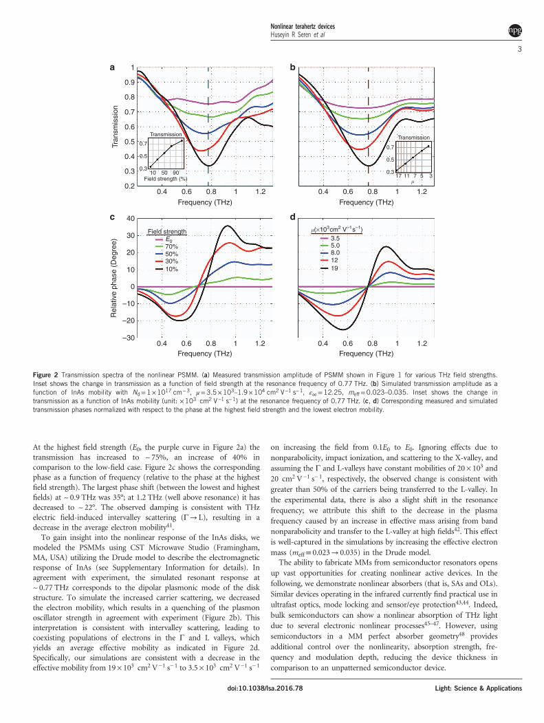
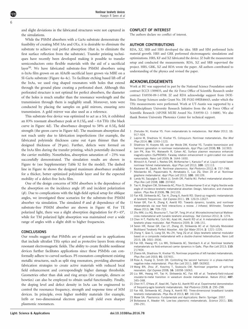
Perfect absorption phenomenon in MM absorbers can be explainedin terms of impedance matching of MM effective parameters8 or interms of interference of the reflected light from resonator and groundplane layers49. The highest absorbance is achieved over a narrow rangeof optimized conditions, with the absorbance becoming weaker (orstronger) as the MM properties are modified. Thus, as the propertiesof the PSMM layer are altered due to nonlinearities the optimalabsorbance conditions change. PSMM absorbers can be designed suchthat the highest absorbance occurs at either low fields or at high fields,resulting in SAs or OLs, respectively.PSMMs in a hexagonal array (70 μm diameter and 90 μm periodi-
city) were made into absorbers by spin coating a polyimide layerfollowed by physical evaporation of a gold ground plane asadditional steps to PSMM fabrication (Figure 3a and 3b). ThePSMM geometry was chosen to obtain a resonance at ~ 0.5 THz,which is close to the peak of our THz high-field source, therebyproviding the largest possible THz field for this nonlinear proof-of-principle demonstration. Two optimized thicknesses were used forthe polyimide spacer layer; for the SA and OL, the thicknesses ofthe polyimide spacer layers were 18 μm and 40 μm, respectively.The SA is designed to maximize the absorption at low-fieldstrengths by taking advantage of the high carrier mobility n-InAs.
The OL is optimized to increase the absorption at higher fieldstrengths where the effective electron mobility is decreased.Importantly, these devices are thinner than a quarter wavelengthat the peak absorption frequency of 0.46 THz (for example,λ/4≈160 μm in free space and 45 μm in GaAs).The ground plane prevents illumination from the front side and has
zero transmission. Thus, the reflection from the absorbers wasmeasured from the bare GaAs side of the device at near-normalincidence. This is shown schematically in Figure 3c. The absorber actsas a Fabry–Perot etalon and produces multiple time resolved THzpulses in the TDS reflection signal. The first reflected pulse is directlyfrom the front surface of the substrate and contains no informationabout the PSMM absorption. To determine the absorption of theactive layer of the PSMM absorber (that is, the internal absorbance),we windowed the data to isolate second reflected pulse, whichcorresponds to the first reflection from the device layer (seeSupplementary Information). As a reference, a sample composed ofa SI-GaAs substrate, polyimide spacer and the ground plane was used.Utilizing the second reflected pulses from both the device and thereference provides a normalized measure of the internal absorbance.We followed the same procedure for the full wave electromagneticsimulations using a time-domain transient solver.
2nd reflected
3rd reflected
1st reflectedIncident
Ground plane MMabsorber
SI-GaAs
SCMMPolyimide
Absorbance
Absorbance
AbsorbanceAbsorbance
Frequency (THz) Frequency (THz)
Field strength
Abs
orba
nce
Abs
orba
nce
SI-GaAssubstrate
a
d
f g
e
b c
11
18 10 6 40.8
0.8
0.6
0.6
0.2
0.4
0.4
1
1
1
0.8
0.8
0.8
0.6
0.6
0.2
0.4
0.4 10.80.60.4
1
0.8
0.6
0.2
0.4
1
0.8
0.6
0.2
0.45.0
0.9
0.9
1
0.8
0.9
0.7
0.5
1317.5
8.0
18.5
10 50 90Field strength (%)
Field strength (%)19 9 5 310 50 90
5030%
20%
70%E0 3.5
5.01015.519
�(x103 cm2 V–1s–1)
�(x103cm2 V–1s–1)
�
�
Figure 3 Nonlinear PSMM absorbers. (a) Schematic view of the PSMM absorber layers. (b) A fabricated PSMM device view from the ground plane side with1 cm2 active area (scale bar=1 cm). (c) Schematic representation of the etalon reflections in the GaAs substrate. Measurements and correspondingsimulation results for (d, e) the SA with 18-μm-thick polyimide layer and (f, g) OL with 40-μm-thick polyimide layer, respectively. d, f share the same legend.Insets show the absorbance trends as a function of field strength and electron mobility (μ) at the frequencies indicated by the dashed lines (mobility unit:×103 cm2 V−1 s−1).
Nonlinear terahertz devicesHuseyin R Seren et al
4
Light: Science & Applications doi:10.1038/lsa.2016.78
The measurement and simulation results are shown in Figure 3d–3gfor the SA and OL absorbers. The absorbance for each device wascalculated by subtracting the reflectance from unity (A= 1− |Ereflected|2),since the transmission through the ground plane was negligible.For the SA, the absorbance at the resonant frequency of 0.5 THzwas 97.5% at low fields (0.2E0, the black curve in Figure 3d).With increasing field strength, the absorbance monotonicallydecreases. At the full strength of the THz beam (E0, the purple curvein Figure 3d), the absorbance was reduced to 49%. Thus, between 0.2and 1.0 E0, a modulation of nearly 50% was obtained. The inset ofFigure 3d shows the change in the absorbance as a function of fieldstrength.The measurement results for the OL are shown in Figure 3f. The
absorbance was 80% at low fields (0.2E0, the black curve in Figure 3f).As the field strength is increased (0.5E0, the blue curve in Figure 3f),the absorbance increased to ~ 99%. Further increasing the fieldstrength up to E0, the absorbance dropped back to 80%, indicatingthat the optimal OL effect for this particular device occurred at 0.5E0.The inset of Figure 3f clearly shows the nonlinear modulation of theabsorbance at 0.46 THz. This reveals a limitation of the present devicein that it exhibits optical limiting behavior up to a certain field value(0.5E0), after which it degrades. Another consequence of using athicker spacer layer in the OL was the observed broadband absorption.
This is mainly because of a second absorption mode arising around1 THz whose tail merged with the fundamental absorption mode.While the modulation was much smaller for the OL in comparison tothe SA, these results nonetheless reveal that it is possible to create bothSAs and OLs from nonlinear MMs.We note that it is possible to improve the optical limiting
capabilities of PSMM with alternative designs. Optimization of theMM geometry (see Supplementary Information for an improved OLdesign example—Supplementary Fig. S7) substantially improves themodulation depth and increases the maximum field at which opticallimiting behavior is maintained. There are, of course, inherentlimitations that exist due the intrinsic properties of the semiconductor.For example, secondary nonlinear processes such as impact ionizationmay take place at even higher fields resulting in a degradation of theabsorption.As in Figure 2, the nonlinear response of the PSMM absorbers were
modeled using the Drude response of n-InAs, with both the mobilityand effective mass used as variable parameters (see SupplementaryTable S1). The overall trends in the simulated absorbances (Figure 3eand 3g) are in good agreement with the measurements. The origin ofthe differences in resonances between experiment and simulation arisefrom several sources. In particular, for the high-field THz reflectancemeasurements, it is difficult to remove artifacts arising from scattering,
Polyimide
PSMM
Gold
1
0.8
0.6
Abs
orba
nce
0.4
0.2
0
Field strength (xE0)
12.5�(x103cm2 V–1s–1)
10.0
7.55.5Perfect Absorbance
0.4 0.6 0.8
1
0.8
0.6
0.4
0.2
0
0.4 0.6Frequency (THz)
TE TM 80
60
40
20
00 0.5 1 1.5 0 0.5 1 1.5
Frequency (THz) Frequency (THz)
� � (d
egre
e)
�
Frequency (THz)
TE TM
0.8 11
15%
20%
30%
50%
a b
d e
f
c
k
EB
k
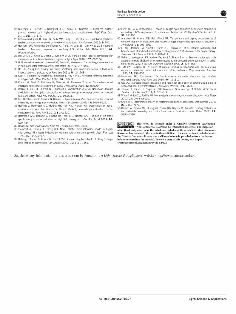
Figure 4 PSMM absorber on flexible substrate. (a) Representative sketch of the flexible semiconductor-based metamaterial absorber. (b) Microscope image ofthe fabricated flexible absorber (scale bar=500 μm). (c) Close-up image of the rings. Rings have 30 μm outer and 15 μm inner radius on average with72.7 μm hexagonal symmetry (scale bar=100 μm). (d) Terahertz-time-domain spectroscopy measurements showing the absorbance for increasing fieldstrength. (e) Simulated absorbance spectra for Drude models with varying mobility and effective mass. (f) Simulated absorbance spectra of substrate-freeabsorber as a function of incidence angle (θ) for TE and TM polarized THz light.
Nonlinear terahertz devicesHuseyin R Seren et al
5
Light: Science & Applicationsdoi:10.1038/lsa.2016.78
and slight deviations in the fabricated structures were not captured inthe simulations.While the PSMM absorbers with a GaAs substrate demonstrate the
feasibility of creating MM SAs and OLs, it is desirable to eliminate thesubstrate to achieve real perfect absorption (that is, to eliminate thefirst surface reflection from the substrate). Transfer printing techni-ques have recently been developed making it possible to transfersemiconductors onto flexible materials with the aid of a sacrificiallayer50. We have fabricated substrate-free PSMM absorbers usingn-InAs film grown on an AlAsSb sacrificial layer grown via MBE on aSI-GaAs substrate (Figure 4a–4c). To facilitate etching based lift-off ofthe InAs, we used ring shaped resonators with holes that extendthrough the ground plane creating a perforated sheet. Although thisperforated structure is not optimal for perfect absorbers, the diameterof the holes is much smaller than the resonance wavelength and thetransmission through them is negligibly small. Moreover, tests wereconducted by placing the samples on gold mirrors, ensuring zerotransmission. A gold mirror was also used as a reference.This substrate-free device was optimized to act as a SA; it exhibited
an 83% resonant absorbance peak at 0.15E0 and ~ 0.6 THz (the blackcurve in Figure 4d). The absorbance dropped to 58% at 0.5E0 fieldstrength (the green curve in Figure 4d). The maximum absorption didnot reach unity due to fabrication imperfections (for example, thefabricated polyimide thickness came out 4 μm thinner than thedesigned thickness of 29 μm). Further, defects were formed onthe InAs film during the transfer printing, which potentially decreasedthe carrier mobility. Nonetheless, absorption saturation of ~ 25% wassuccessfully demonstrated. The simulation results are shown inFigure 4e (see Supplementary Table S2 for the model). The dashedline in Figure 4e shows the designed maximum absorbance availablefor a thicker, better optimized polyimide layer and for the expectedmobility of a defect-free InAs film.One of the design concerns of MM absorbers is the dependence of
the absorption on the incidence angle (θ) and incident polarization(ϕ). Due to complications with the high-field optical setup for obliqueangles, we investigated these scenarios for the substrate-free PSMMabsorber via simulation. The simulated θ and ϕ dependence of thesubstrate-free PSMM absorber are shown in Figure 4f. For TEpolarized light, there was a slight absorption degradation for θ445°,while for TM polarized light absorption was maintained over a widerange of angles with a slight shift to higher frequencies.
CONCLUSIONS
Our results suggest that PSMMs are of potential use in applicationsthat include ultrafast THz optics and as protective layers from strongresonant electromagnetic fields. The ability to create flexible nonlineardevices further facilitates applications since these PSMMs can con-formally adhere to curved surfaces. PS resonators complement existingmetallic structures, such as split ring resonators, providing alternativefabrication strategies to create active materials with reduced localfield enhancement and correspondingly higher damage thresholds.Geometries other than disk and ring arrays (for example, dimers orbowties) can also be employed to obtain useful functionality. Finally,the doping level and defect density in InAs can be engineered tocontrol the resonance frequency, strength and response time of MMdevices. In principle, even higher mobility materials (for example,InSb or two-dimensional electron gases) will yield even sharperplasmonic resonances.
CONFLICT OF INTERESTThe authors declare no conflict of interest.
AUTHOR CONTRIBUTIONS
RDA, XZ, SRB and HRS developed the idea. SRB and SJM performed InAsmaterial growth. HRS and GRK performed electromagnetic simulations and
optimizations. HRS, KF and XZ fabricated the device. JZ built the measurement
setup and conducted the measurements. RDA, XZ and SRB supervised the
project. HRS, GRK, XZ and RDA wrote the paper. All authors contributed to
understanding of the physics and revised the paper.
ACKNOWLEDGEMENTSWork at BU was supported in part by the National Science Foundation under
contract ECCS 1309835, and the Air Force Office of Scientific Research under
contract FA9550-09-1-0708. JZ and RDA acknowledge support from DOE-
Basic Energy Sciences under Grant No. DE-FG02-09ER46643, under which the
THz measurements were performed. Work at UT-Austin was supported by a
Multidisciplinary University Research Initiative from the Air Force Office of
Scientific Research (AFOSR MURI Award No. FA9550-12- 1-0488). We also
thank Boston University Photonics Center for technical support.
1 Zheludev NI, Kivshar YS. From metamaterials to metadevices. Nat Mater 2012; 11:917–924.
2 Lapine M, Shadrivov IV, Kivshar YS. Colloquium: Nonlinear metamaterials. Rev ModPhys 2014; 86: 1093–1123.
3 Shadrivov IV, Kozyrev AB, van der Weide DW, Kivshar YS. Tunable transmission andharmonic generation in nonlinear metamaterials. Appl Phys Lett 2008; 93: 161903.
4 Jain PK, Xiao YH, Walsworth R, Cohen AE. Surface plasmon resonance enhancedmagneto-optics (SuPREMO): Faraday rotation enhancement in gold-coated iron oxidenanocrystals. Nano Lett 2009; 9: 1644–1650.
5 Minovich A, Farnell J, Neshev DN, McKerracher I, Karouta F et al. Liquid crystal basednonlinear fishnet metamaterials. Appl Phys Lett 2012; 100: 121113.
6 Kauranen M, Zayats AV. Nonlinear plasmonics. Nat Photonics 2012; 6: 737–748.7 Nikolaenko AE, Papasimakis N, Atmatzakis E, Luo ZQ, Shen ZX et al. Nonlinear
graphene metamaterial. Appl Phys Lett 2012; 100: 181109.8 Landy NI, Sajuyigbe S, Mock JJ, Smith DR, Padilla WJ. Perfect metamaterial absorber.
Phys Rev Lett 2008; 100: 207402.9 Tao H, Bingham CM, Strikwerda AC, Pilon D, Shrekenhamer D et al. Highly flexible wide
angle of incidence terahertz metamaterial absorber: Design, fabrication, and character-ization. Phys Rev B 2008; 78: 241103.
10 Fan KB, Strikwerda AC, Tao H, Zhang X, Averitt RD. Stand-up magnetic metamaterialsat terahertz frequencies. Opt Express 2011; 19: 12619–12627.
11 Keiser GR, Fan K, Zhang X, Averitt RD. Towards dynamic, tunable, and nonlinearmetamaterials via near field interactions: a review. J Infrared, Millimeter, TerahertzWaves 2013; 34: 709–723.
12 Zhu WM, Liu AQ, Bourouina T, Tsai DP, Teng JH et al.Microelectromechanical Maltese-cross metamaterial with tunable terahertz anisotropy. Nat Commun 2012; 3: 1274.
13 Chen H-T, Padilla WJ, Cich MJ, Azad AK, Averitt RD et al. A metamaterial solid-stateterahertz phase modulator. Nat Photonics 2009; 3: 148–151.
14 Seren HR, Keiser GR, Cao LY, Zhang JD, Strikwerda AC et al. Optically ModulatedMultiband Terahertz Perfect Absorber. Adv Opt Mater 2014; 2: 1221–1226.
15 Zhang Y, Qiao S, Liang SX, Wu ZH, Yang ZQ et al. Gbps terahertz external modulatorbased on a composite metamaterial with a double-channel heterostructure. Nano Lett2015; 15: 3501–3506.
16 Fan KB, Hwang HY, Liu MK, Strikwerda AC, Sternbach A et al. Nonlinear terahertzmetamaterials via field-enhanced carrier dynamics in GaAs. Phys Rev Lett 2013; 110:217404.
17 Zharov AA, Shadrivov IV, Kivshar YS. Nonlinear properties of left-handed metamaterials.Phys Rev Lett 2003; 91: 037401.
18 Rose A, Huang D, Smith DR. Controlling the second harmonic in a phase-matchednegative-index metamaterial. Phys Rev Lett 2011; 107: 063902.
19 Wang BN, Zhou JF, Koschny T, Soukoulis CM. Nonlinear properties of split-ringresonators. Opt Express 2008; 16: 16058–16063.
20 Liu MK, Hwang HY, Tao H, Strikwerda AC, Fan KB et al. Terahertz-field-inducedinsulator-to-metal transition in vanadium dioxide metamaterial. Nature 2012; 487:345–348.
21 Chen H-T, O'Hara JF, Azad AK, Taylor AJ, Averitt RD et al. Experimental demonstrationof frequency-agile terahertz metamaterials. Nat Photonics 2008; 2: 295–298.
22 Fan KB, Strikwerda AC, Zhang X, Averitt RD. Three-dimensional broadband tunableterahertz metamaterials. Phys Rev B 2013; 87: 161104.
23 Maier SA. Plasmonics: Fundamentals and Applications. Berlin: Springer. 2007.24 Boltasseva A, Atwater HA. Low-loss plasmonic metamaterials. Science 2011; 331:
290–291.
Nonlinear terahertz devicesHuseyin R Seren et al
6
Light: Science & Applications doi:10.1038/lsa.2016.78
25 Guilengui VT, Cerutti L, Rodriguez J-B, Tournié E, Taliercio T. Localized surfaceplasmon resonances in highly doped semiconductors nanostructures. Appl. Phys. Lett.2012; 101: 161113.
26 Sensale-Rodriguez B, Yan RS, Kelly MM, Fang T, Tahy K et al. Broadband grapheneterahertz modulators enabled by intraband transitions. Nat Commun 2012; 3: 780.
27 Hanham SM, Fernández-Domínguez AI, Teng JH, Ang SS, Lim KP et al. Broadbandterahertz plasmonic response of touching InSb disks. Adv Mater 2012; 24:OP226–OP230.
28 Bai Q, Liu C, Chen J, Cheng C, Kang M et al. Tunable slow light in semiconductormetamaterial in a broad terahertz regime. J Appl Phys 2010; 107: 093104.
29 Hoffman AJ, Alekseyev L, Howard SS, Franz KJ, Wasserman D et al. Negative refractionin semiconductor metamaterials. Nat Mater 2007; 6: 946–950.
30 Ho I-C, Zhang X-C. Driving intervalley scattering and impact ionization in InAs withintense terahertz pulses. Appl Phys Lett 2011; 98: 241908.
31 Gaal P, Reimann K, Woerner M, Elsaesser T, Hey R et al. Nonlinear terahertz responseof n-type GaAs. Phys Rev Lett 2006; 96: 187402.
32 Kuehn W, Gaal P, Reimann K, Woerner M, Elsaesser T et al. Terahertz-inducedinterband tunneling of electrons in GaAs. Phys Rev B 2010; 82: 075204.
33 Razzari L, Su FH, Sharma G, Blanchard F, Ayesheshim A et al. Nonlinear ultrafastmodulation of the optical absorption of intense few-cycle terahertz pulses in n-dopedsemiconductors. Phys Rev B 2009; 79: 193204.
34 Su FH, Blanchard F, Sharma G, Razzari L, Ayesheshim A et al. Terahertz pulse inducedintervalley scattering in photoexcited GaAs. Opt Express 2009; 17: 9620–9629.
35 Hebling J, Hoffmann MC, Hwang HY, Yeh K-L, Nelson KA. Observation of none-quilibrium carrier distribution in Ge, Si, and GaAs by terahertz pump-terahertz probemeasurements. Phys Rev B 2010; 81: 035201.
36 Hoffmann MC, Hebling J, Hwang HY, Yeh K-L, Nelson KA. THz-pump/THz-probespectroscopy of semiconductors at high field strengths. J Opt Soc Am B 2009; 26:A29–A34.
37 Boyd RW. Nonlinear Optics. New York: Academic Press. 2003.38 Trampert A, Tournié E, Ploog KH. Novel plastic strain-relaxation mode in highly
mismatched III-V layers induced by two-dimensional epitaxial growth. Appl Phys Lett1995; 66: 2265–2267.
39 Hebling J, Almási G, Kozma IZ, Kuhl J. Velocity matching by pulse front tilting for largearea THz-pulse generation. Opt Express 2002; 10: 1161–1166.
40 Hirori H, Doi A, Blanchard F, Tanaka K. Single-cycle terahertz pulses with amplitudesexceeding 1 MV/cm generated by optical rectification in LiNbO3. Appl Phys Lett 2011;98: 091106.
41 Arabshahi H, Khalvati MR, Rokn-Abadi MR. Temperature and doping dependencies ofelectron mobility in InAs, AlAs and AlGaAs at high electric field application. Brazilian JPhys 2008; 38: 293–296.
42 Li YB, Stradling RA, Knight T, Birch JR, Thomas RH et al. Infrared reflection andtransmission of undoped and Si-doped InAs grown on GaAs by molecular beam epitaxy.Semicond Sci Technol 1999; 8: 101–111.
43 Keller U, Weingarten KJ, Kartner FX, Kopf D, Braun B et al. Semiconductor saturableabsorber mirrors (SESAM’s) for femtosecond to nanosecond pulse generation in solid-state lasers. IEEE J Sel Top Quantum Electron 1996; 2: 435–453.
44 Tutt LW, Boggess TF. A review of optical limiting mechanisms and devices usingorganics, fullerenes, semiconductors and other materials. Prog Quantum Electron1993; 17: 299–338.
45 Hoffmann MC, Turchinovich D. Semiconductor saturable absorbers for ultrafastterahertz signals. Appl Phys Lett 2010; 96: 151110.
46 Cao JC. Interband impact ionization and nonlinear absorption of terahertz radiation insemiconductor heterostructures. Phys Rev Lett 2003; 91: 237401.
47 Tanaka K, Hirori H, Nagai M. THz Nonlinear Spectroscopy of Solids. IEEE TransTerahertz Sci Technol 2011; 1: 301–312.
48 Watts CM, Liu XL, Padilla WJ. Metamaterial electromagnetic wave absorbers. Adv Mater2012; 24: OP98–OP120.
49 Chen H-T. Interference theory of metamaterial perfect absorbers. Opt Express 2012;20: 7165–7172.
50 Carlson A, Bowen AM, Huang YG, Nuzzo RG, Rogers JA. Transfer printing techniquesfor materials assembly and micro/nanodevice fabrication. Adv Mater 2012; 24:5284–5318.
This work is licensed under a Creative Commons Attribution-NonCommercial-NoDerivs 4.0 International License. The images or
other third party material in this article are included in the article’s Creative Commonslicense, unless indicated otherwise in the credit line; if the material is not included underthe Creative Commons license, users will need to obtain permission from the licenseholder to reproduce the material. To view a copy of this license, visit http://creativecommons.org/licenses/by-nc-nd/4.0/
Supplementary Information for this article can be found on the Light: Science & Applications' website (http://www.nature.com/lsa).
Nonlinear terahertz devicesHuseyin R Seren et al
7
Light: Science & Applicationsdoi:10.1038/lsa.2016.78