Embed Size (px)
Citation preview
Novel electromagnetic structures for high frequency acceleration
(Part 1-3)
Rosa Letizia
Lancaster University/ Cockcroft Institute
Cockcroft Institute, Spring term, 6/03/17
CI lectures, Spring term 1
Lecture 1 – Introduction to high frequency dielectric acceleration• Novel accelerating structures• Dielectric laser acceleration• Important parameters
Lecture 2 – Photonic crystal technology• What is a photonic crystal• Bandgap property• Intentional defects in Photonic Crystals• Photonic crystal cavities and waveguides
Lecture 3 – Properties of photonic structures for acceleration • Photonic crystal structures• Wakefields in dielectrics• Requirements and challenges• THz laser acceleration
Lectures outline
CI lectures, Spring term 2
Lecture 4 – Introduction to Metamaterials• Novel electromagnetic properties• Dispersion engineering• Metamaterials loaded waveguides• Potential application in accelerators
Lecture 5 – Introduction to Plasmonic waveguiding• Surface plasmon polariton• Dispersion • Plasmonic waveguide• Accelerators applications
Lecture 6 – Introduction to Finite Difference Time Domain• Time domain computational modelling• Finite Difference Time Domain• Examples
Lectures outline
CI lectures, Spring term 3
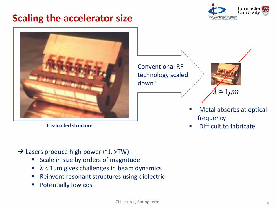
Iris-loaded structure
Conventional RF technology scaled down?
Metal absorbs at optical frequency
Difficult to fabricate
m 1
Lasers produce high power (~J, >TW) Scale in size by orders of magnitude λ < 1um gives challenges in beam dynamics Reinvent resonant structures using dielectric Potentially low cost
Scaling the accelerator size
CI lectures, Spring term 4
Recent demonstrations
800 nm period550 µm structures
Energy ≈ 190-250 MeV per meter
CI lectures, Spring term 5
Recent demonstrations
CI lectures, Spring term 6
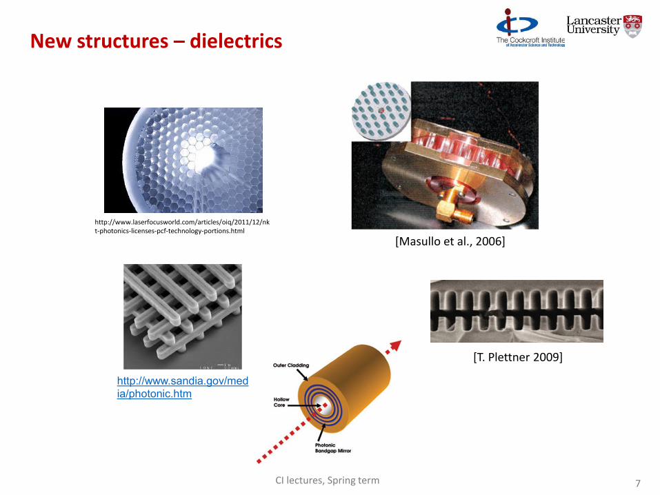
New structures – dielectrics
CI lectures, Spring term 7
http://www.laserfocusworld.com/articles/oiq/2011/12/nkt-photonics-licenses-pcf-technology-portions.html
[T. Plettner 2009]
[Masullo et al., 2006]
http://www.sandia.gov/media/photonic.htm
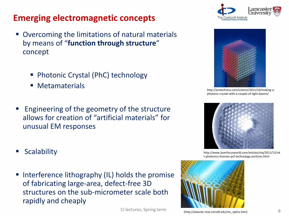
Overcoming the limitations of natural materials by means of “function through structure” concept
Photonic Crystal (PhC) technology
Metamaterials
Engineering of the geometry of the structure allows for creation of “artificial materials” for unusual EM responses
Scalability
Interference lithography (IL) holds the promise of fabricating large-area, defect-free 3D structures on the sub-micrometer scale both rapidly and cheaply
Emerging electromagnetic concepts
http://arstechnica.com/science/2011/10/making-a-photonic-crystal-with-a-couple-of-light-beams/
http://www.laserfocusworld.com/articles/oiq/2011/12/nkt-photonics-licenses-pcf-technology-portions.html
[http://wiesner.mse.cornell.edu/res_optics.htm]CI lectures, Spring term 8
Dielectric accelerators
Types:
Dielectric wall acceleration
Dielectric wakefield acceleration
Dielectric laser acceleration
Dielectric assisted waveguide
Dielectric loaded waveguides
Advantages:
High breakdown threshold (1-5 GV/m)
High frequency operation
Can reduce wakefields (photonic crystals)
Mature fabrication technologies available
CI lectures, Spring term 9
Dielectric laser accelerators
Typically refers to accelerators concepts operating at optical frequencies, driven by lasers in all- dielectric structures
Acceleration of any particle by fields requires equal amount of energy taken out of em fields
Requirements for the accelerating mode:
Speed-of-light TM mode
The non existence of metal boundaries allows structures to damp high order modes
CI lectures, Spring term 10
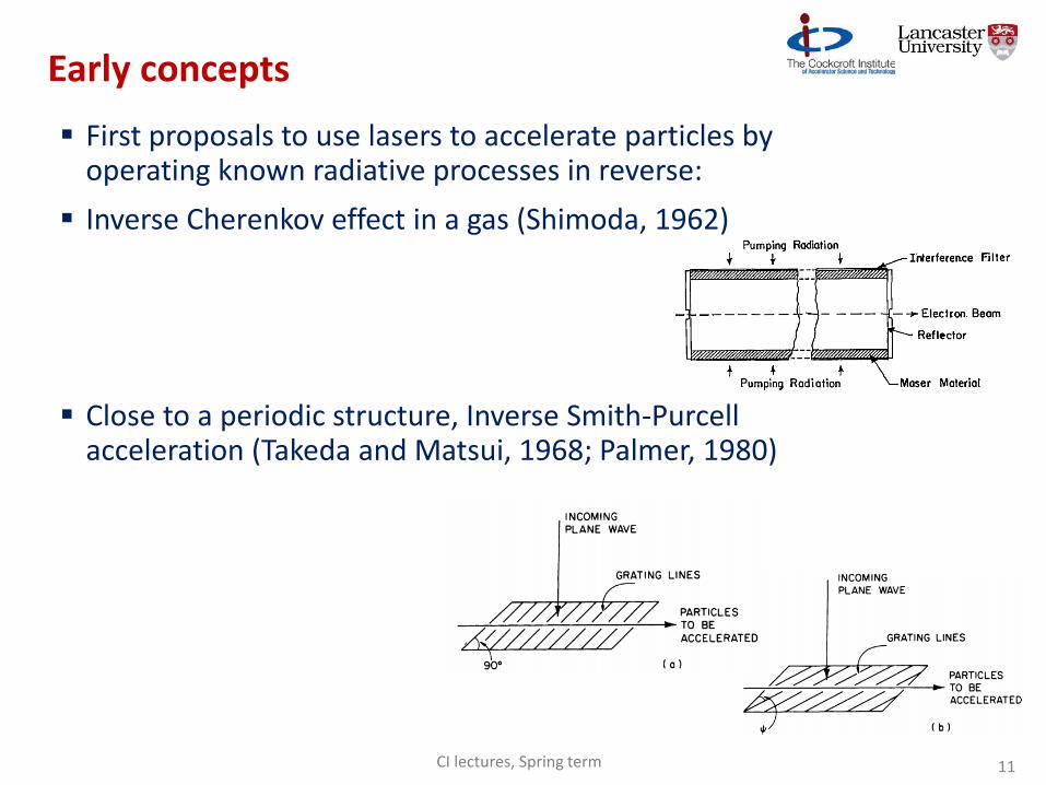
First proposals to use lasers to accelerate particles by operating known radiative processes in reverse:
Inverse Cherenkov effect in a gas (Shimoda, 1962)
Close to a periodic structure, Inverse Smith-Purcell acceleration (Takeda and Matsui, 1968; Palmer, 1980)
Early concepts
CI lectures, Spring term 11
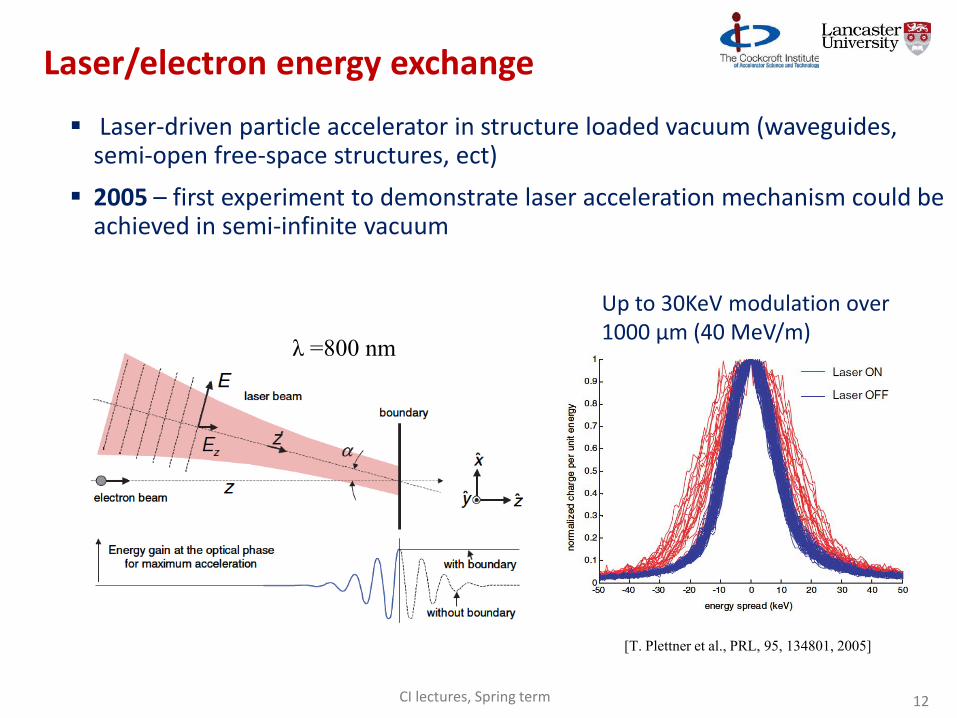
Laser-driven particle accelerator in structure loaded vacuum (waveguides, semi-open free-space structures, ect)
2005 – first experiment to demonstrate laser acceleration mechanism could be achieved in semi-infinite vacuum
Up to 30KeV modulation over 1000 µm (40 MeV/m)
[T. Plettner et al., PRL, 95, 134801, 2005]
λ =800 nm
Laser/electron energy exchange
CI lectures, Spring term 12
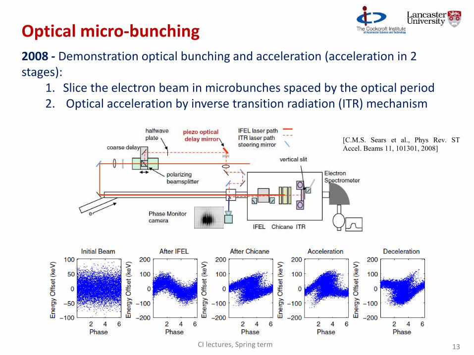
[C.M.S. Sears et al., Phys Rev. STAccel. Beams 11, 101301, 2008]
2008 - Demonstration optical bunching and acceleration (acceleration in 2 stages):
1. Slice the electron beam in microbunches spaced by the optical period2. Optical acceleration by inverse transition radiation (ITR) mechanism
Optical micro-bunching
CI lectures, Spring term 13
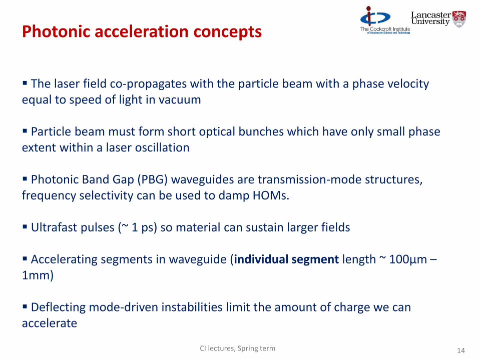
The laser field co-propagates with the particle beam with a phase velocity equal to speed of light in vacuum
Particle beam must form short optical bunches which have only small phase extent within a laser oscillation
Photonic Band Gap (PBG) waveguides are transmission-mode structures, frequency selectivity can be used to damp HOMs.
Ultrafast pulses (~ 1 ps) so material can sustain larger fields
Accelerating segments in waveguide (individual segment length ~ 100µm –1mm)
Deflecting mode-driven instabilities limit the amount of charge we can accelerate
Photonic acceleration concepts
CI lectures, Spring term 14
All-dielectric accelerating structures
A range of proposals:
Lin (2001)
Mizrahi and Schachter (2004)
Plettner, Lu, Byer (2006)
Cowan (2008)
Naranjo et al. (2012)
First demonstration - Peralta et al. (2013)
CI lectures, Spring term 15
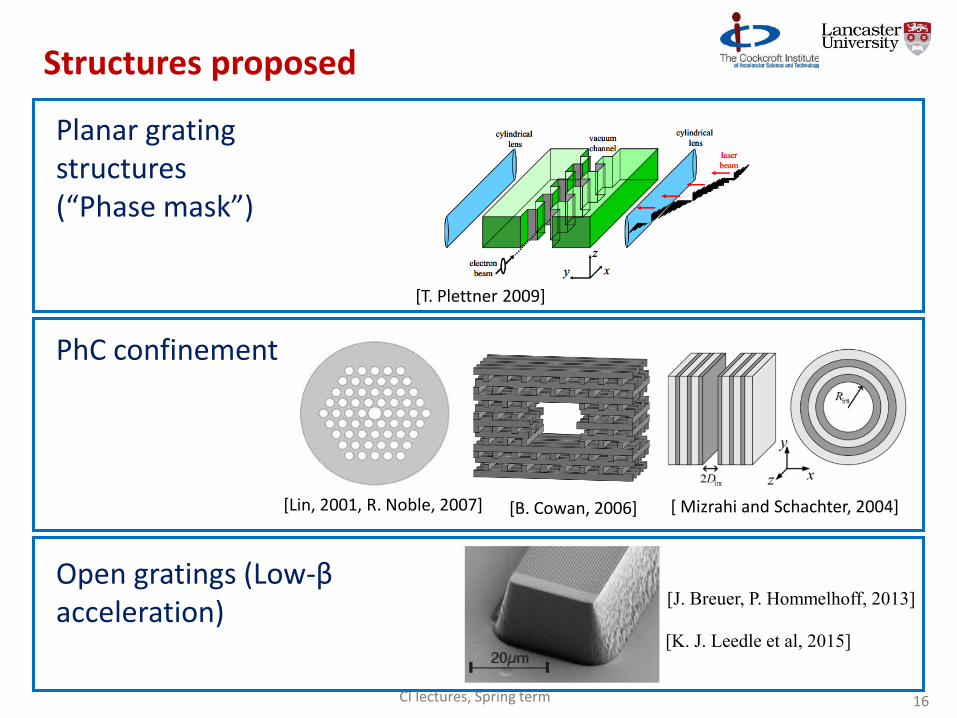
Structures proposed
Planar grating structures(“Phase mask”)
PhC confinement
Open gratings (Low-βacceleration)
[T. Plettner 2009]
[B. Cowan, 2006][Lin, 2001, R. Noble, 2007]
[K. J. Leedle et al, 2015]
[ Mizrahi and Schachter, 2004]
[J. Breuer, P. Hommelhoff, 2013]
CI lectures, Spring term 16
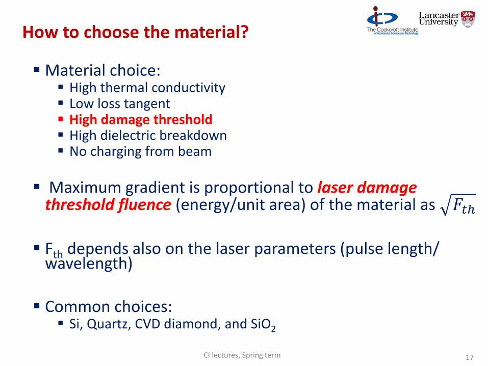
How to choose the material?
Material choice: High thermal conductivity Low loss tangent High damage threshold High dielectric breakdown No charging from beam
Maximum gradient is proportional to laser damage threshold fluence (energy/unit area) of the material as 𝐹𝑡ℎ
Fth depends also on the laser parameters (pulse length/ wavelength)
Common choices: Si, Quartz, CVD diamond, and SiO2
CI lectures, Spring term 17
𝜔𝑙𝑎𝑠𝑒𝑟 = 𝜔𝑝 =4𝜋𝑛𝑒𝑒
2
𝑚∗
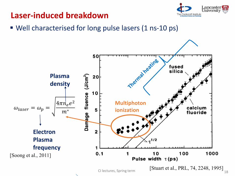
Well characterised for long pulse lasers (1 ns-10 ps)
Plasma density
Electron Plasma frequency
[Stuart et al., PRL, 74, 2248, 1995]
[Soong et al., 2011]
Laser-induced breakdown
Multiphoton ionization
CI lectures, Spring term 18
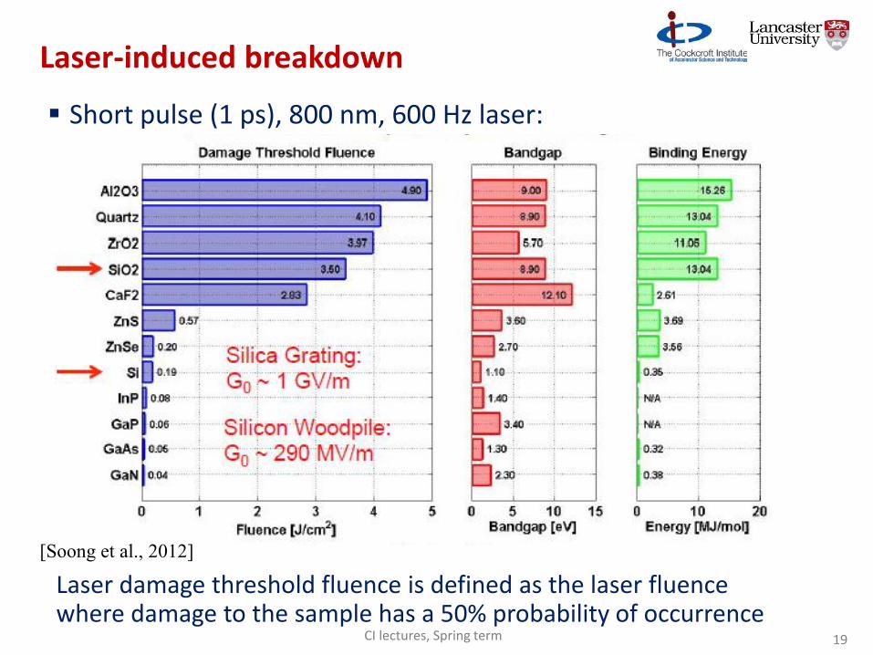
Laser damage threshold fluence is defined as the laser fluencewhere damage to the sample has a 50% probability of occurrence
Short pulse (1 ps), 800 nm, 600 Hz laser:
Laser-induced breakdown
[Soong et al., 2012]
CI lectures, Spring term 19
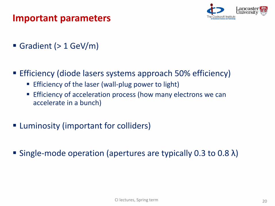
Important parameters
Gradient (> 1 GeV/m)
Efficiency (diode lasers systems approach 50% efficiency) Efficiency of the laser (wall-plug power to light)
Efficiency of acceleration process (how many electrons we can accelerate in a bunch)
Luminosity (important for colliders)
Single-mode operation (apertures are typically 0.3 to 0.8 λ)
CI lectures, Spring term 20
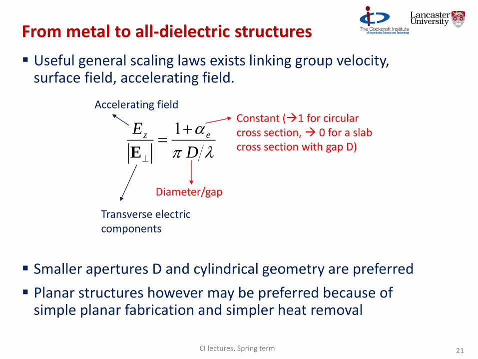
From metal to all-dielectric structures
Useful general scaling laws exists linking group velocity, surface field, accelerating field.
Smaller apertures D and cylindrical geometry are preferred
Planar structures however may be preferred because of simple planar fabrication and simpler heat removal
D
E ez
1E
Diameter/gap
Constant (1 for circular cross section, 0 for a slab cross section with gap D)
Transverse electric components
Accelerating field
CI lectures, Spring term 21
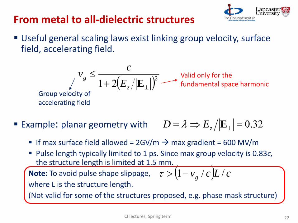
From metal to all-dielectric structures
Useful general scaling laws exist linking group velocity, surface field, accelerating field.
Example: planar geometry with
If max surface field allowed = 2GV/m max gradient = 600 MV/m
Pulse length typically limited to 1 ps. Since max group velocity is 0.83c, the structure length is limited at 1.5 mm.
Note: To avoid pulse shape slippage,
where L is the structure length.
(Not valid for some of the structures proposed, e.g. phase mask structure)
221
Ez
g
E
cv Valid only for the
fundamental space harmonic
Group velocity of accelerating field
32.0 EzED
cLcvg //1
CI lectures, Spring term 22
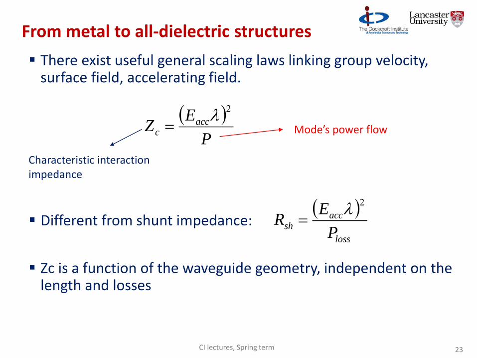
From metal to all-dielectric structures
There exist useful general scaling laws linking group velocity, surface field, accelerating field.
Different from shunt impedance:
Zc is a function of the waveguide geometry, independent on the length and losses
P
EZ acc
c
2
Mode’s power flow
Characteristic interaction impedance
loss
accsh
P
ER
2
CI lectures, Spring term 23

Structures proposed
Planar grating structures(“Phase mask”)
PhC confinement
Open gratings (Low-βacceleration)
[T. Plettner 2009]
[B. Cowan, 2006][Lin, 2001, R. Noble, 2007]
[K. J. Leedle et al, 2015]
[ Mizrahi and Schachter, 2004]
[J. Breuer, P. Hommelhoff, 2013]
CI lectures, Spring term 24
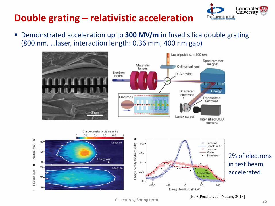
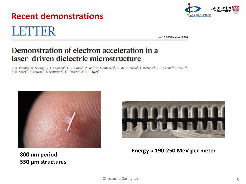
[E. A Peralta et al, Nature, 2013]
Demonstrated acceleration up to 300 MV/m in fused silica double grating (800 nm, …laser, interaction length: 0.36 mm, 400 nm gap)
Double grating – relativistic acceleration
2% of electrons in test beam accelerated.
CI lectures, Spring term 25
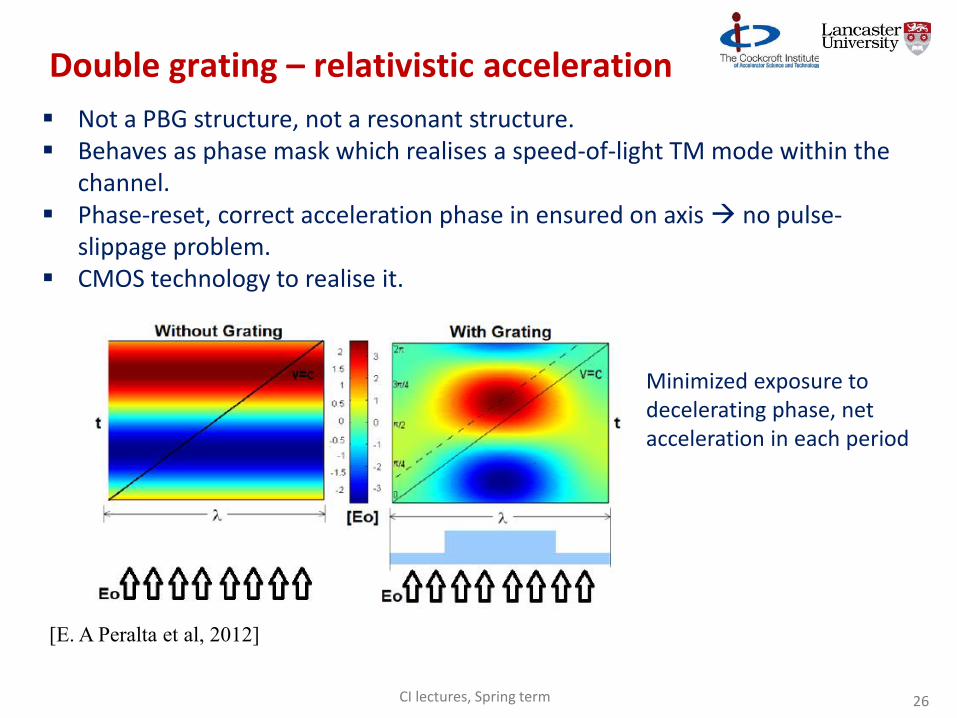
Not a PBG structure, not a resonant structure. Behaves as phase mask which realises a speed-of-light TM mode within the
channel. Phase-reset, correct acceleration phase in ensured on axis no pulse-
slippage problem. CMOS technology to realise it.
Double grating – relativistic acceleration
[E. A Peralta et al, 2012]
Minimized exposure to decelerating phase, net acceleration in each period
CI lectures, Spring term 26
Novel electromagnetic structures for high frequency acceleration
(Part 2)
Rosa Letizia
Lancaster University/ Cockcroft Institute
Cockcroft Institute, Spring term, 6/03/17
CI lectures, Spring term 27
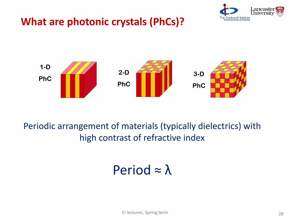
Periodic arrangement of materials (typically dielectrics) with high contrast of refractive index
Period ≈ λ
1-D
PhC
What are photonic crystals (PhCs)?
CI lectures, Spring term 28
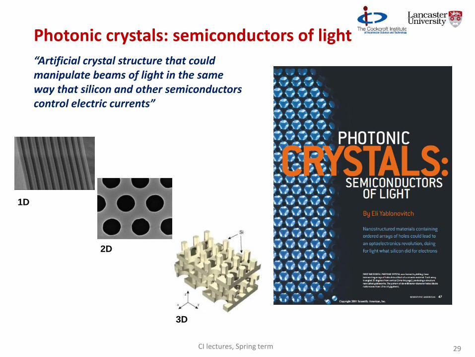
“Artificial crystal structure that couldmanipulate beams of light in the sameway that silicon and other semiconductors control electric currents”
1D
2D
3D
Photonic crystals: semiconductors of light
CI lectures, Spring term 29
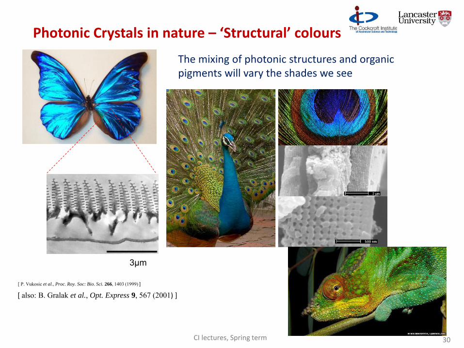
Photonic Crystals in nature – ‘Structural’ colours
3µm
[ P. Vukosic et al., Proc. Roy. Soc: Bio. Sci. 266, 1403 (1999) ]
[ also: B. Gralak et al., Opt. Express 9, 567 (2001) ]
The mixing of photonic structures and organic pigments will vary the shades we see
CI lectures, Spring term 30
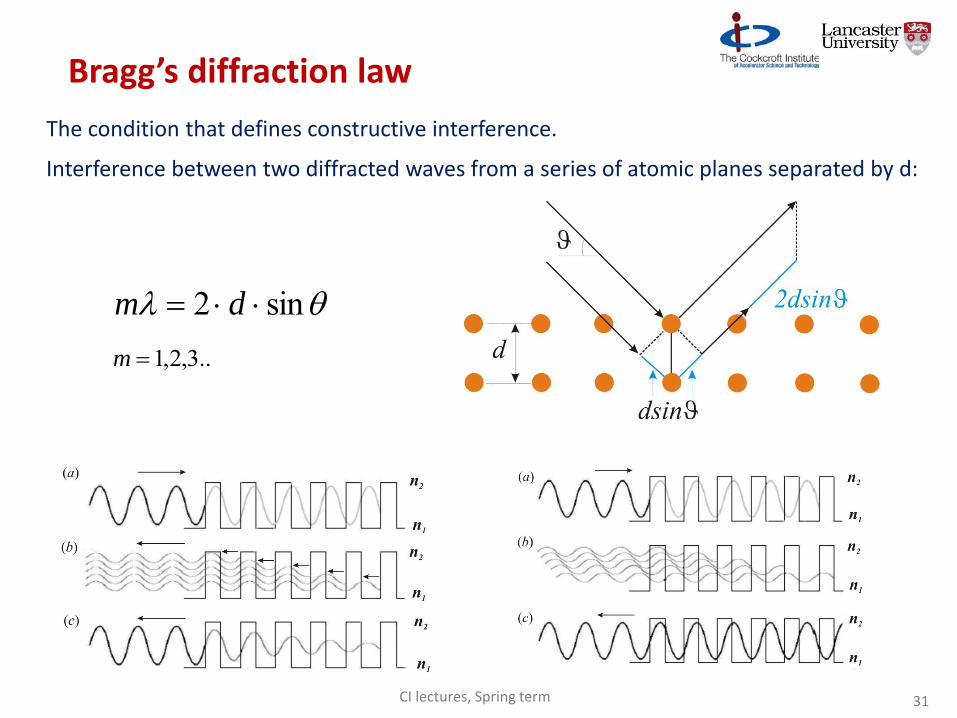
The condition that defines constructive interference.
sin2 dm
..3,2,1m
Interference between two diffracted waves from a series of atomic planes separated by d:
Bragg’s diffraction law
CI lectures, Spring term 31
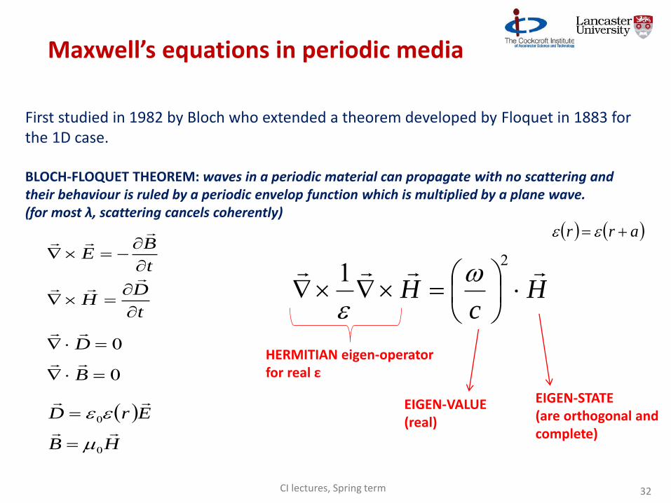
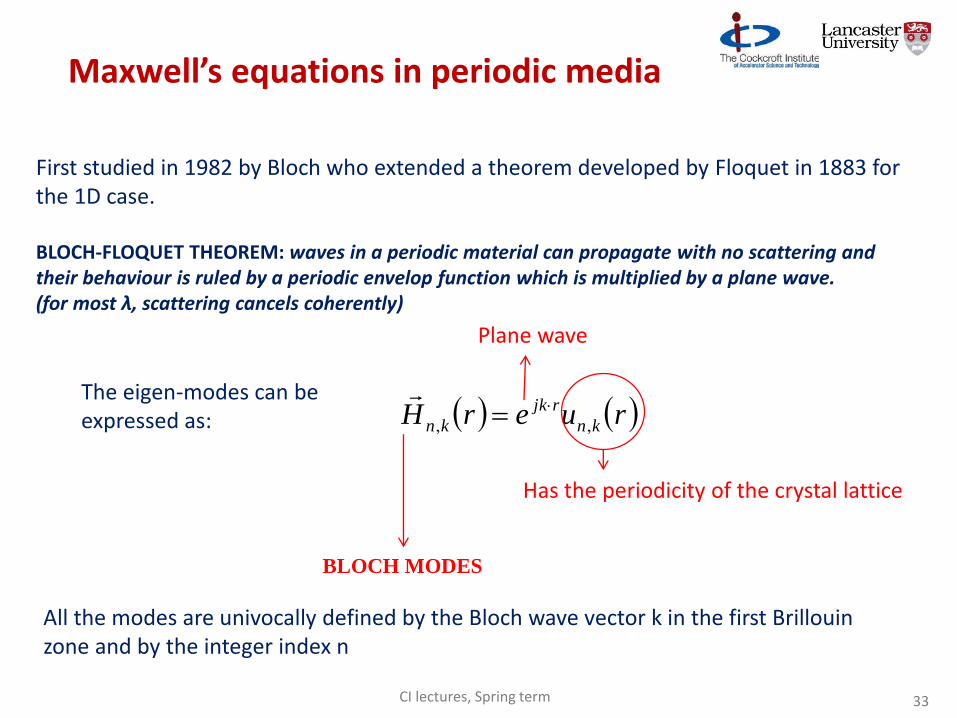
First studied in 1982 by Bloch who extended a theorem developed by Floquet in 1883 for the 1D case.
BLOCH-FLOQUET THEOREM: waves in a periodic material can propagate with no scattering and their behaviour is ruled by a periodic envelop function which is multiplied by a plane wave. (for most λ, scattering cancels coherently)
t
BE
t
DH
0 D
0 B
ErD
0
HB
0
Hc
H
21
arr
HERMITIAN eigen-operatorfor real ε
EIGEN-VALUE(real)
EIGEN-STATE(are orthogonal and complete)
Maxwell’s equations in periodic media
CI lectures, Spring term 32
ruerH kn
rjk
kn ,,
Has the periodicity of the crystal lattice
Plane wave
BLOCH MODES
First studied in 1982 by Bloch who extended a theorem developed by Floquet in 1883 for the 1D case.
BLOCH-FLOQUET THEOREM: waves in a periodic material can propagate with no scattering and their behaviour is ruled by a periodic envelop function which is multiplied by a plane wave. (for most λ, scattering cancels coherently)
The eigen-modes can be expressed as:
All the modes are univocally defined by the Bloch wave vector k in the first Brillouin zone and by the integer index n
Maxwell’s equations in periodic media
CI lectures, Spring term 33
G
rjk
Ger
r
1
G
rGkjkn
Gkn eurH )(,,
,' ,'2
2,
'kn
G
G
nkn
GGG uc
kuGkGk
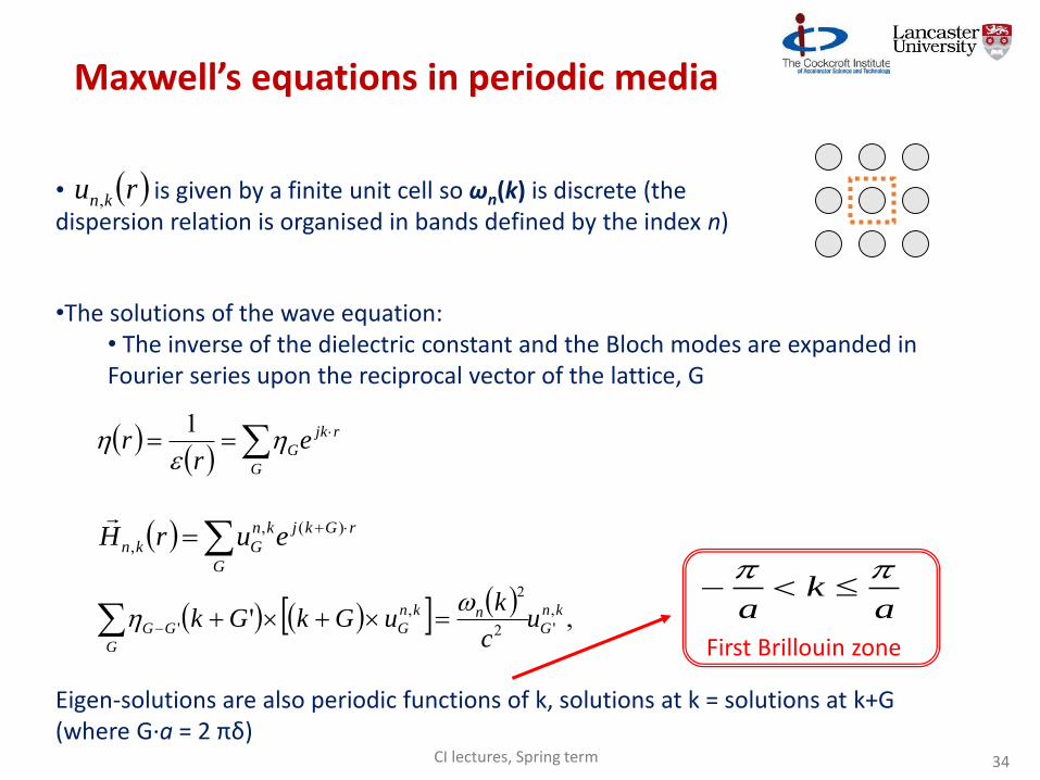
• is given by a finite unit cell so ωn(k) is discrete (the dispersion relation is organised in bands defined by the index n)
•The solutions of the wave equation:• The inverse of the dielectric constant and the Bloch modes are expanded in Fourier series upon the reciprocal vector of the lattice, G
ak
a
First Brillouin zone
ru kn,
Eigen-solutions are also periodic functions of k, solutions at k = solutions at k+G(where G∙a = 2 πδ)
Maxwell’s equations in periodic media
CI lectures, Spring term 34
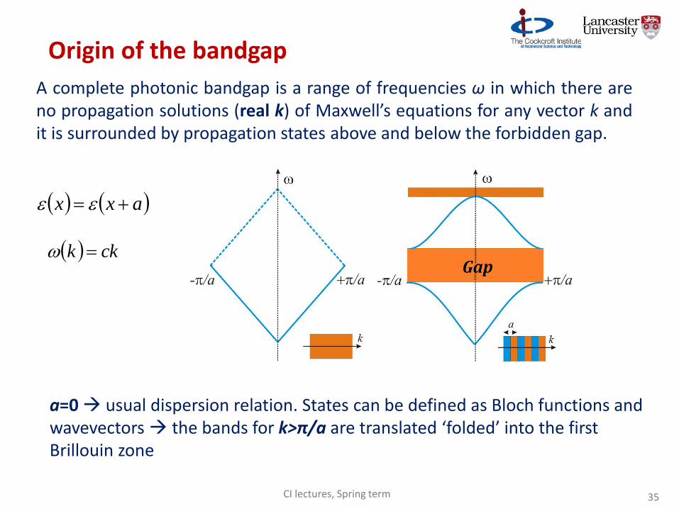
A complete photonic bandgap is a range of frequencies ω in which there areno propagation solutions (real k) of Maxwell’s equations for any vector k andit is surrounded by propagation states above and below the forbidden gap.
ckk
axx
a=0 usual dispersion relation. States can be defined as Bloch functions and wavevectors the bands for k>π/a are translated ‘folded’ into the first Brillouin zone
Origin of the bandgap
CI lectures, Spring term 35
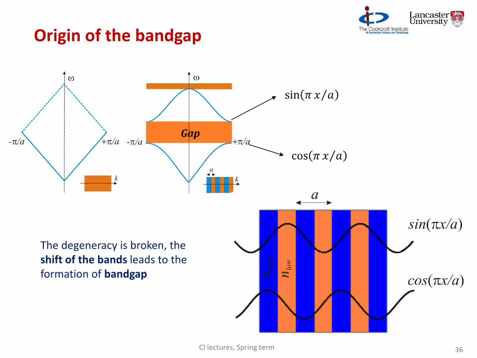
sin 𝜋 𝑥 𝑎
cos 𝜋 𝑥 𝑎
The degeneracy is broken, the shift of the bands leads to the formation of bandgap
Origin of the bandgap
CI lectures, Spring term 36
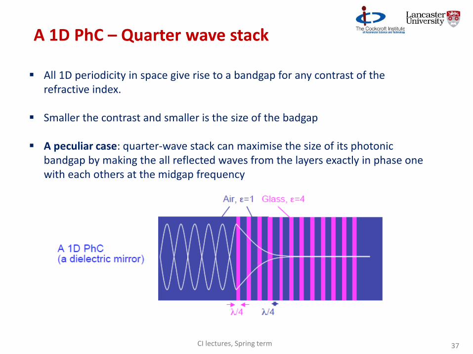
All 1D periodicity in space give rise to a bandgap for any contrast of the refractive index.
Smaller the contrast and smaller is the size of the badgap
A peculiar case: quarter-wave stack can maximise the size of its photonic bandgap by making the all reflected waves from the layers exactly in phase one with each others at the midgap frequency
A 1D PhC – Quarter wave stack
CI lectures, Spring term 37
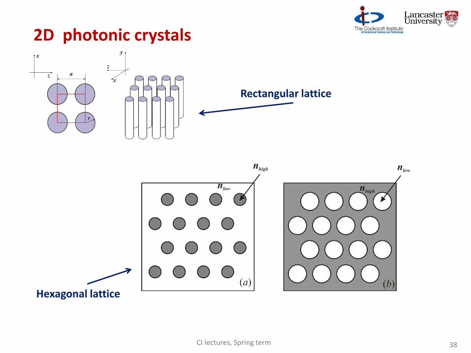
Rectangular lattice
Hexagonal lattice
2D photonic crystals
CI lectures, Spring term 38
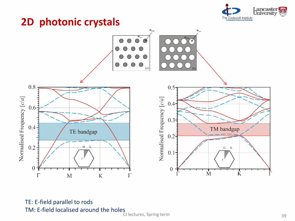
TE: E-field parallel to rodsTM: E-field localised around the holes
2D photonic crystals
CI lectures, Spring term 39
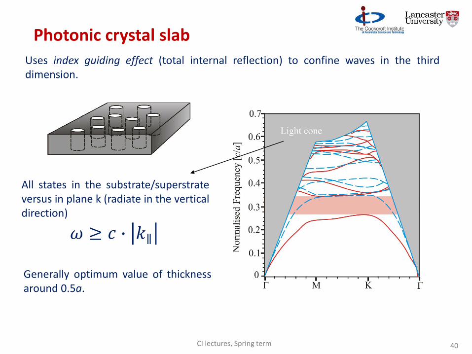
Uses index guiding effect (total internal reflection) to confine waves in the thirddimension.
Generally optimum value of thicknessaround 0.5a.
All states in the substrate/superstrateversus in plane k (radiate in the verticaldirection)
𝜔 ≥ 𝑐 ∙ 𝑘∥
Photonic crystal slab
CI lectures, Spring term 40
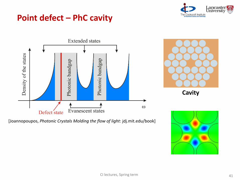
Cavity
[Joannopoupos, Photonic Crystals Molding the flow of light: jdj.mit.edu/book]
Point defect – PhC cavity
CI lectures, Spring term 41
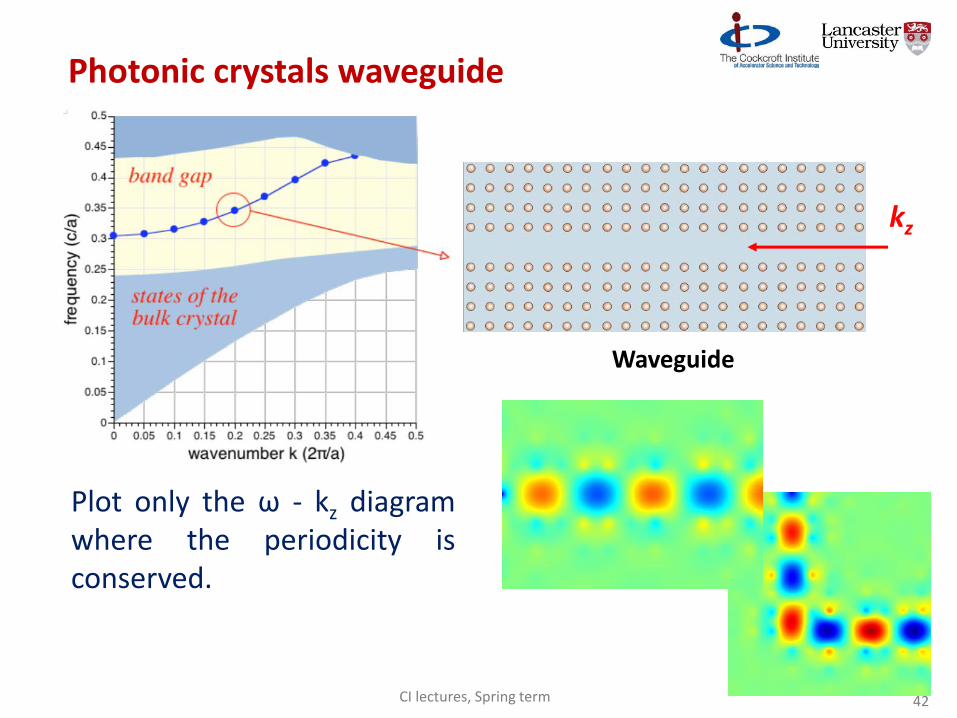
Waveguide
Photonic crystals waveguide
Plot only the ω - kz diagramwhere the periodicity isconserved.
kz
CI lectures, Spring term 42
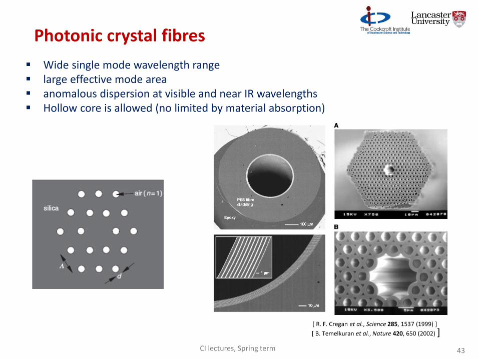
Wide single mode wavelength range large effective mode area anomalous dispersion at visible and near IR wavelengths Hollow core is allowed (no limited by material absorption)
[ B. Temelkuran et al., Nature 420, 650 (2002) ][ R. F. Cregan et al., Science 285, 1537 (1999) ]
Photonic crystal fibres
CI lectures, Spring term 43
Good confinement depends on the contrast of dielectric constant within the PhC and thickness of the PhC surrounding the defect.
PhC waveguides and cavities have much larger transverse size than metallic structures (typically order of a single wavelength).
In PhC stuctures the defect “modes” do not behave exactly as TM modes, however in the centre of the vacuum channel the emproperties of these “modes” are very similar to those of accelerating modes in metal cavities.
Photonic crystal confinement
CI lectures, Spring term 44
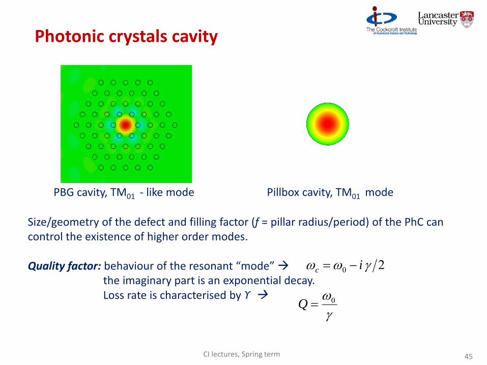
Photonic crystals cavity
PBG cavity, TM01 - like mode Pillbox cavity, TM01 mode
Size/geometry of the defect and filling factor (f = pillar radius/period) of the PhC can control the existence of higher order modes.
Quality factor: behaviour of the resonant “mode” the imaginary part is an exponential decay. Loss rate is characterised by ϒ
20 ic
0Q
CI lectures, Spring term 45
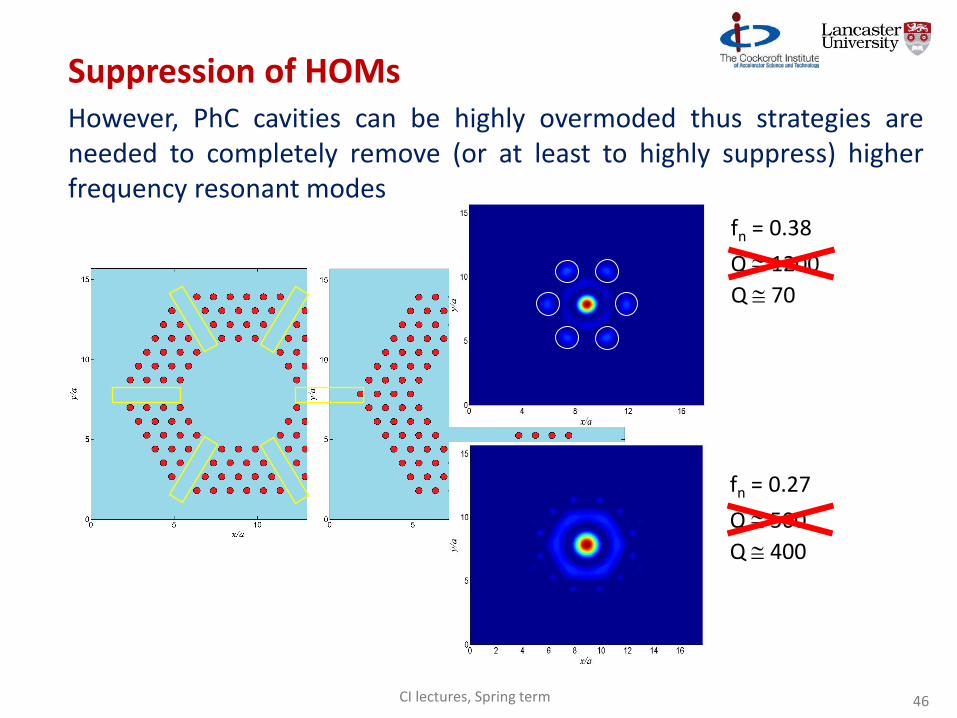
However, PhC cavities can be highly overmoded thus strategies areneeded to completely remove (or at least to highly suppress) higherfrequency resonant modes
fn = 0.38
Q 1200
fn = 0.27
Q 500
Q 70
Q 400
Suppression of HOMs
CI lectures, Spring term 46
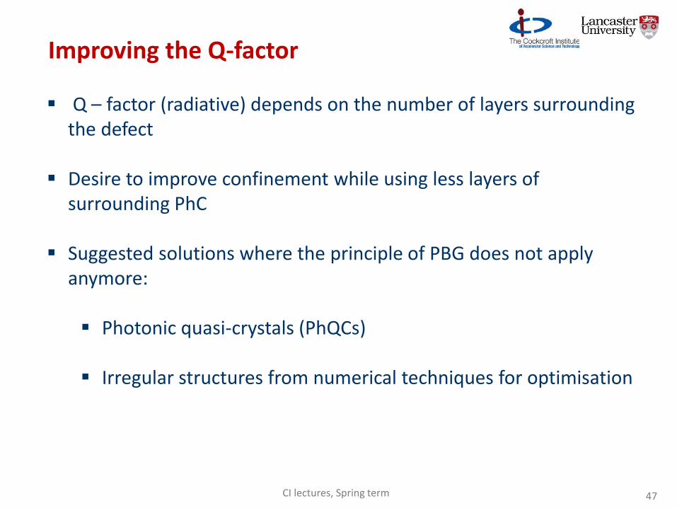
Q – factor (radiative) depends on the number of layers surrounding the defect
Desire to improve confinement while using less layers of surrounding PhC
Suggested solutions where the principle of PBG does not apply anymore:
Photonic quasi-crystals (PhQCs)
Irregular structures from numerical techniques for optimisation
Improving the Q-factor
CI lectures, Spring term 47
18 sapphire rods in optimised position increased Q (radiative) from 130 to 104
No self-consistent theory to calculate the optimum arrangement, result of numerical techniques for optimisation
More sensitive to rod positions (tighter tolerances)
[Bauer, Werner and Cary, 2008 and 2016]
Improving the Q-factor
CI lectures, Spring term 48
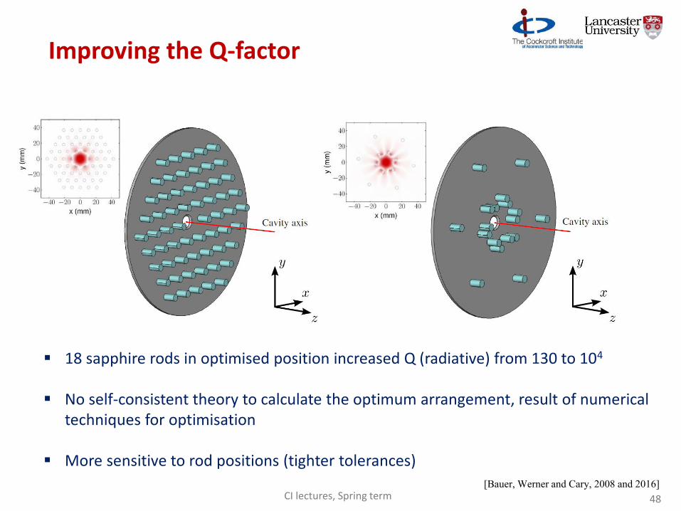
“Photonic quasicrystals” (PQCs) are based on the so-called aperiodic-tiling geometriescharacterised by weak rotational symmetry of “non-crystallographic” type.
In PQCs, the EM response can be strongly dependent on the lattice short-rangeconfiguration and an additional degree of freedom for design can come from aperiodicity.
In terms of quality factor, the quasycristal PhC cavity outperform the counterparthexagonal lattice PhC
* E. Di Gennaro, et al., Appl. Phys. Lett., 93, 164102 (2009)
A prototype of a PQC has been fabricated and tested and it has been shown that hybrid-dielectric structures can be successfully exploited for the design of high-gradientaccelerators*
Photonic quasi-crystals
CI lectures, Spring term 49
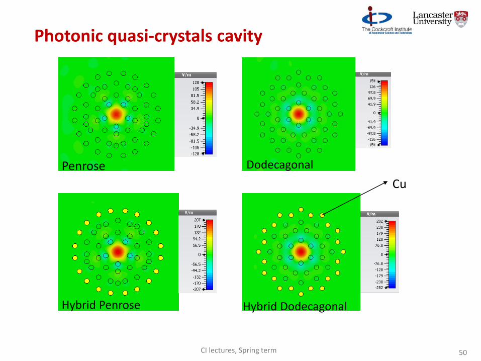
Photonic quasi-crystals cavity
Penrose Dodecagonal
Hybrid Dodecagonal
Cu
Hybrid Penrose
CI lectures, Spring term 50
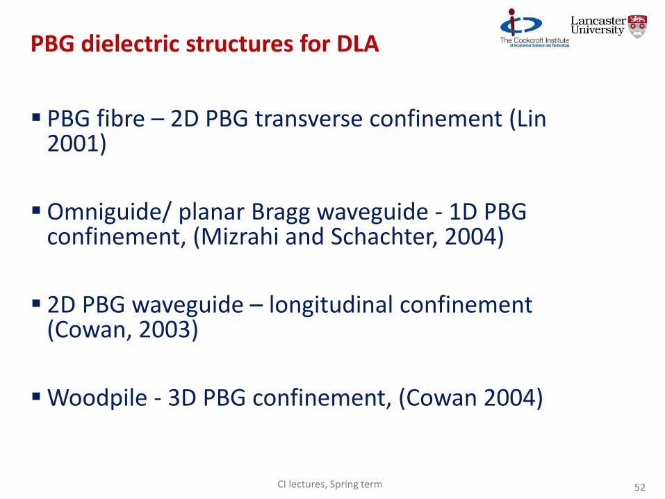
PBG dielectric structures for DLA
PBG fibre – 2D PBG transverse confinement (Lin 2001)
Omniguide/ planar Bragg waveguide - 1D PBG confinement, (Mizrahi and Schachter, 2004)
2D PBG waveguide – longitudinal confinement (Cowan, 2003)
Woodpile - 3D PBG confinement, (Cowan 2004)
CI lectures, Spring term 52

Novel electromagnetic structures for high frequency acceleration
(Part 3)
Rosa Letizia
Lancaster University/ Cockcroft Institute
Cockcroft Institute, Spring term, 6/03/17
CI lectures, Spring term 53
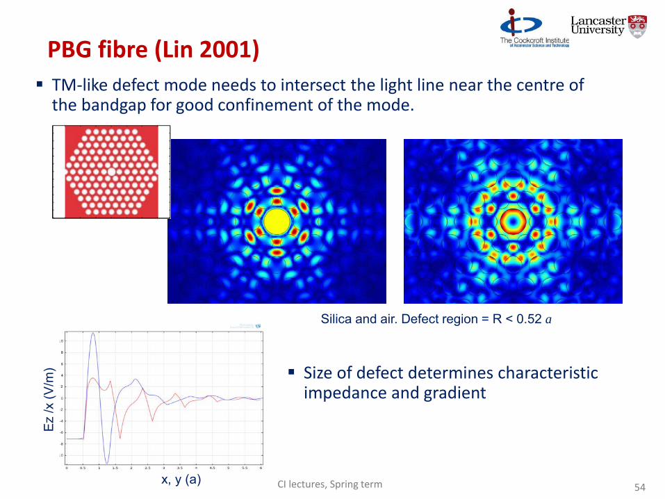
PBG fibre (Lin 2001)
TM-like defect mode needs to intersect the light line near the centre of the bandgap for good confinement of the mode.
x, y (a)
Ez
/x (V
/m)
Silica and air. Defect region = R < 0.52 a
Size of defect determines characteristic impedance and gradient
CI lectures, Spring term 54
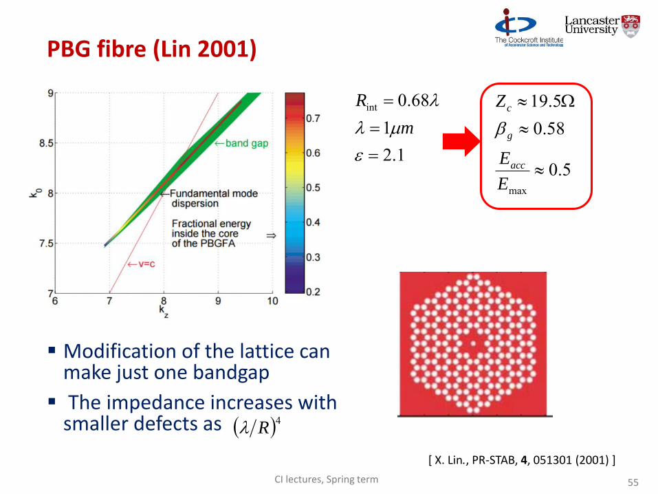
PBG fibre (Lin 2001)
Modification of the lattice can make just one bandgap
The impedance increases with smaller defects as
[ X. Lin., PR-STAB, 4, 051301 (2001) ]
1.21
68.0int
m
R
5.0
58.05.19
max
E
E
Z
acc
g
c
4R
CI lectures, Spring term 55
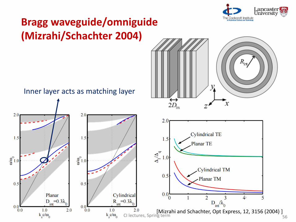
Bragg waveguide/omniguide(Mizrahi/Schachter 2004)
[Mizrahi and Schachter, Opt Express, 12, 3156 (2004) ]
Inner layer acts as matching layer
CI lectures, Spring term 56
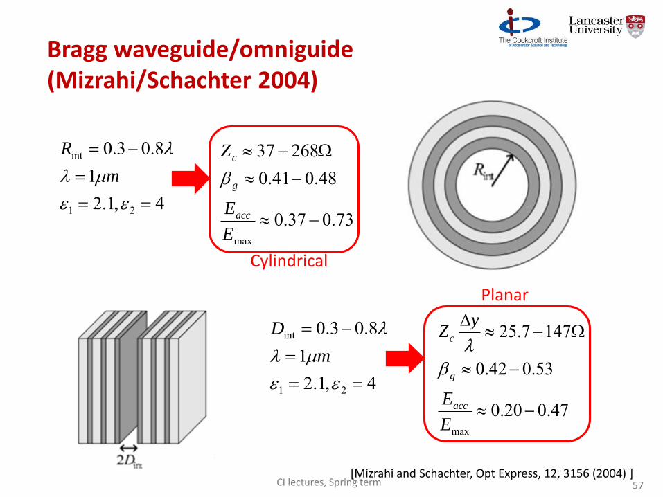
Bragg waveguide/omniguide(Mizrahi/Schachter 2004)
4,1.21
8.03.0
21
int
m
R
73.037.0
48.041.026837
max
E
E
Z
acc
g
c
Cylindrical
4,1.21
8.03.0
21
int
m
D
47.020.0
53.042.0
1477.25
max
E
E
yZ
acc
g
c
Planar
[Mizrahi and Schachter, Opt Express, 12, 3156 (2004) ]CI lectures, Spring term 57
Unit cell: 4 layers
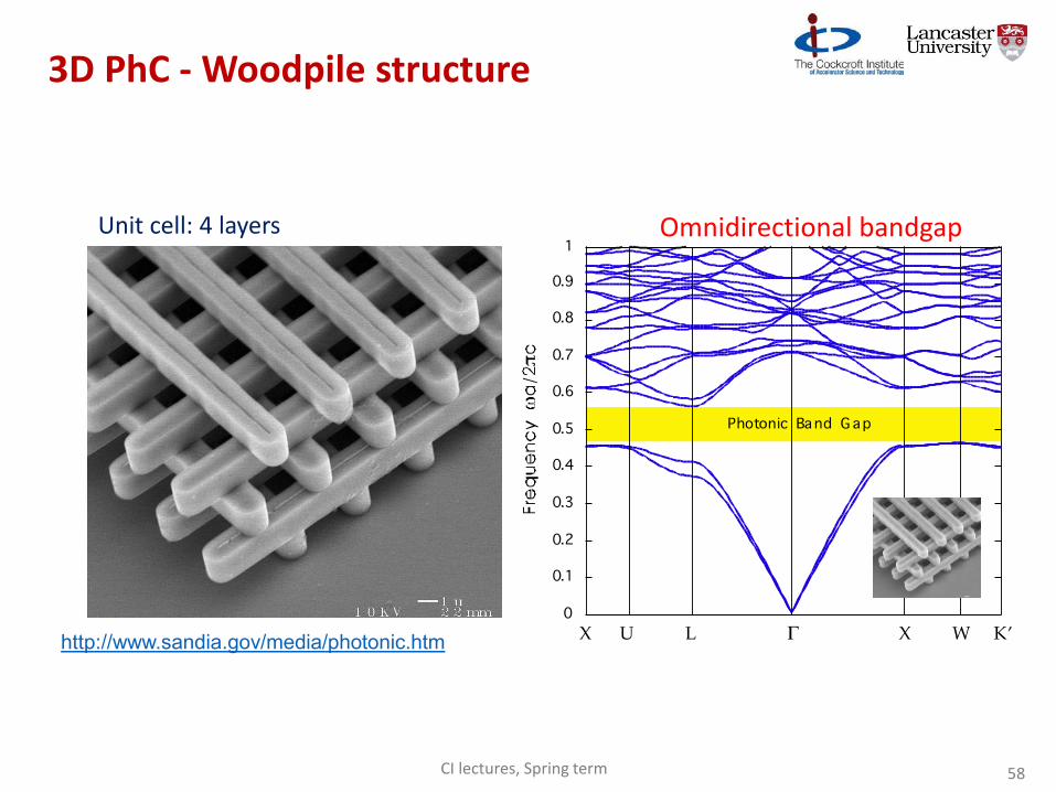
3D PhC - Woodpile structure
Omnidirectional bandgap
http://www.sandia.gov/media/photonic.htm
CI lectures, Spring term 58
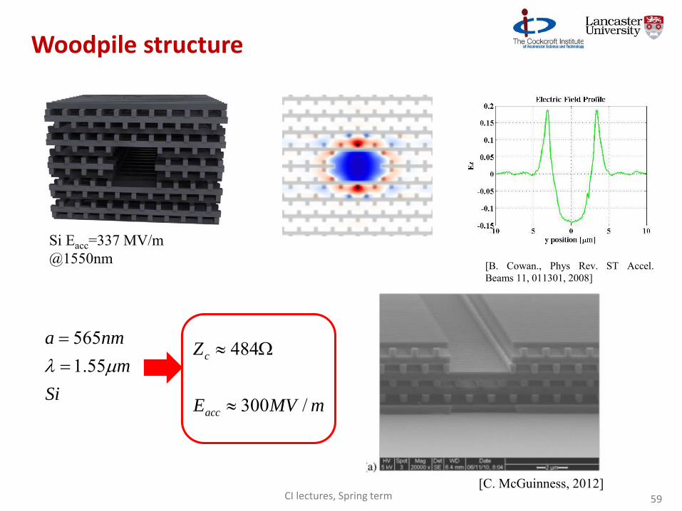
Si Eacc=337 MV/m @1550nm [B. Cowan., Phys Rev. ST Accel.
Beams 11, 011301, 2008]
Woodpile structure
Si
m
nma
55.1565
mMVE
Z
acc
c
/300
484
[C. McGuinness, 2012]CI lectures, Spring term 59
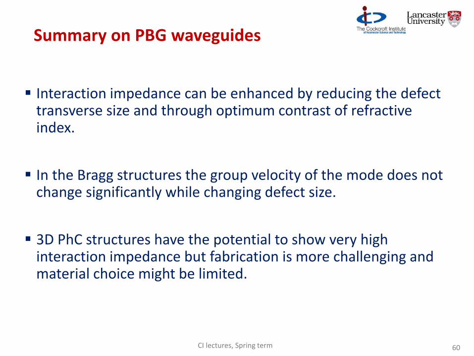
Summary on PBG waveguides
Interaction impedance can be enhanced by reducing the defect transverse size and through optimum contrast of refractive index.
In the Bragg structures the group velocity of the mode does not change significantly while changing defect size.
3D PhC structures have the potential to show very high interaction impedance but fabrication is more challenging and material choice might be limited.
CI lectures, Spring term 60
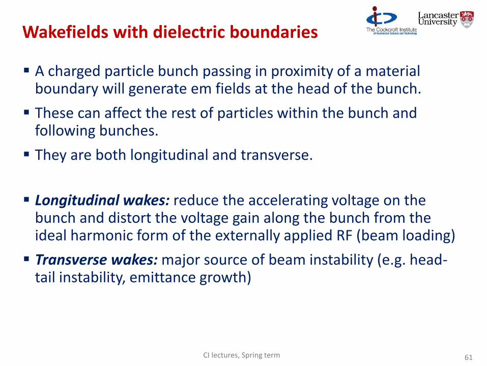
Wakefields with dielectric boundaries
A charged particle bunch passing in proximity of a material boundary will generate em fields at the head of the bunch.
These can affect the rest of particles within the bunch and following bunches.
They are both longitudinal and transverse.
Longitudinal wakes: reduce the accelerating voltage on the bunch and distort the voltage gain along the bunch from the ideal harmonic form of the externally applied RF (beam loading)
Transverse wakes: major source of beam instability (e.g. head-tail instability, emittance growth)
CI lectures, Spring term 61
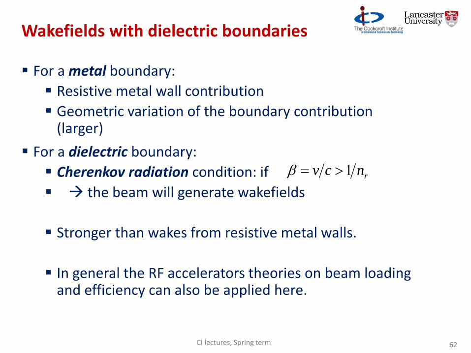
Wakefields with dielectric boundaries
For a metal boundary:
Resistive metal wall contribution
Geometric variation of the boundary contribution (larger)
For a dielectric boundary:
Cherenkov radiation condition: if
the beam will generate wakefields
Stronger than wakes from resistive metal walls.
In general the RF accelerators theories on beam loading and efficiency can also be applied here.
rncv 1
CI lectures, Spring term 62
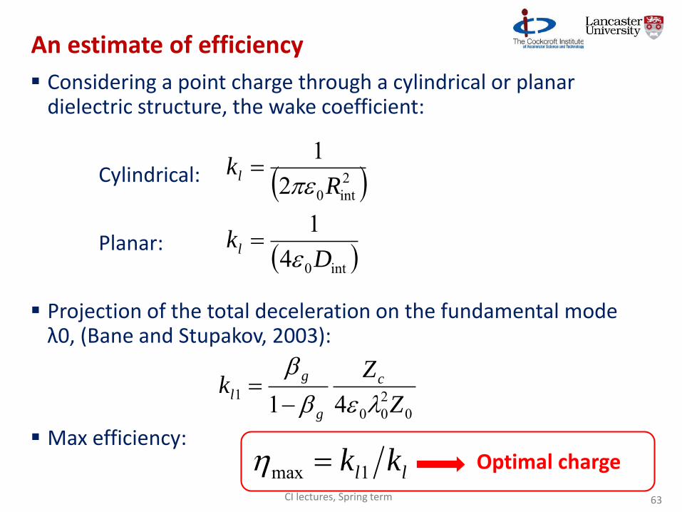
An estimate of efficiency
Considering a point charge through a cylindrical or planar dielectric structure, the wake coefficient:
Cylindrical:
Planar:
Projection of the total deceleration on the fundamental mode λ0, (Bane and Stupakov, 2003):
Max efficiency:
int0
2int0
41
21
Dk
Rk
l
l
0200
1 41 Z
Zk c
g
g
l
ll kk 1max Optimal charge
CI lectures, Spring term 63
113
31112
22
222
max
gg
g
ggt
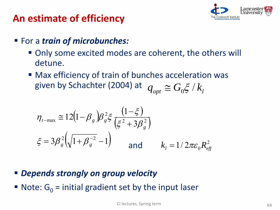
For a train of microbunches:
Only some excited modes are coherent, the others will detune.
Max efficiency of train of bunches acceleration was given by Schachter (2004) at
and
Depends strongly on group velocity
Note: G0 = initial gradient set by the input laser
lopt kGq /0
202/1 effl Rk
An estimate of efficiency
CI lectures, Spring term 64
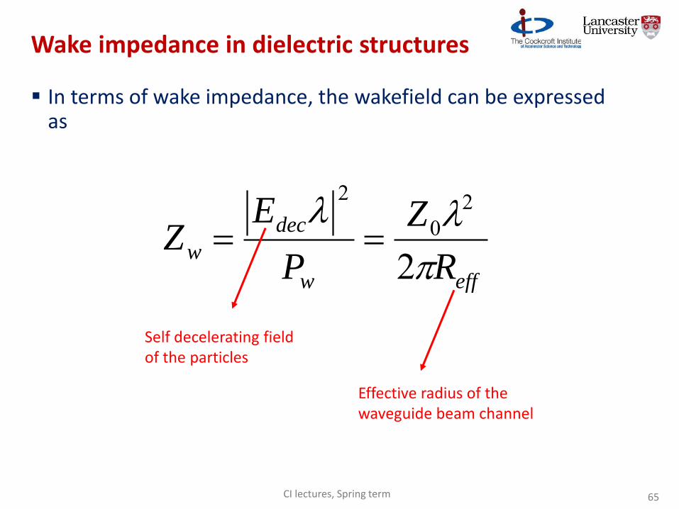
Wake impedance in dielectric structures
effw
dec
wR
Z
P
EZ
2
20
2
Self decelerating field of the particles
In terms of wake impedance, the wakefield can be expressed as
Effective radius of the waveguide beam channel
CI lectures, Spring term 65
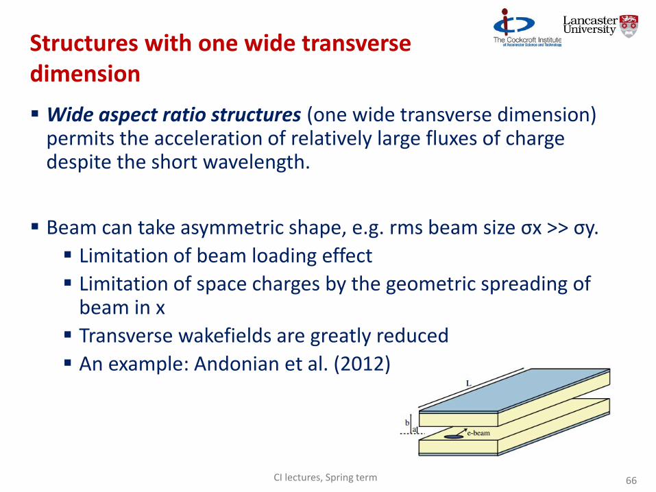
Structures with one wide transverse dimension
Wide aspect ratio structures (one wide transverse dimension) permits the acceleration of relatively large fluxes of charge despite the short wavelength.
Beam can take asymmetric shape, e.g. rms beam size σx >> σy.
Limitation of beam loading effect
Limitation of space charges by the geometric spreading of beam in x
Transverse wakefields are greatly reduced
An example: Andonian et al. (2012)
CI lectures, Spring term 66
Requirements on the electron beam
Optical structures naturally have sub-fs time scales and favour high repetition rate operation
Typical e- beam required: bunch charge 10-20 fC, bunch length < 1ps, bunch radius has to match the transverse size of the optical accelerating structure, energy of 1 MeV, repetition rate > 10 MHz.
The bunch length is much longer than accelerating wavelength the optical accelerator produces bunches with a very large energy spread.
To improve the quality of the e- beam and make a more efficient use of the initial charge the beam should be “micro-bunched” (particles need to fit individual acceleration buckets).
CI lectures, Spring term 67
Injection: low-beta DLA structures
Low-beta DLA structures are relevant as pre-acceleration stage (from tens of keV to 1 MeV) to solve the low-energy injection problem
Also applications for proton, ion acceleration
Structure geometry needs to change as particle velocity increases (synchronous approach)
Asynchronous approach also possible
Mm-wave Mizuno et al (1987)
Mc Neur et al (2012)
NIR, Breuer and Hommelhoff (2014)
CI lectures, Spring term 68
Demonstrated acceleration of 28 keV electrons in open grating of fused silica (110 fs, 800 nm laser) gradient up to 25 MV/m
a: grating period
n: order of the spatial harmonic
Demonstrated acceleration of 96 keVelectrons in silicon open grating (130 fs, 907 nm laser) up to 200 MeV/m
Laser
e-
𝛽𝑐 = 𝑣𝑝ℎ =𝑐𝑎
𝑛𝜆
𝛽 =𝑎
𝑛𝜆
Synchronism:
[J. Breuer, P. Hommelhoff, 2013]Thin metal coating to prevent charging
[K. J. Leedle et al, 2015]
Sub-relativistic acceleration
CI lectures, Spring term 69
Structures:
Dephasing
Damage threshold
Heat dissipation at the outer boundaries (planar structures may be preferred at optical frequency)
Materials:
Degradation with high field and radiation exposure
Charging and multipactoring
Thermal conductivity of the material
Nonlinear polarizability and Raman scattering
Limitations on structures and materials
CI lectures, Spring term 70
Terahertz acceleration
To achieve GV/m, only need THz frequency acceleration
Significant increase of beam quality
Main challenges in this range: Metal displays high losses the design of high-Q cavities
is precluded and dissipated energy at the metal walls is much higher than at RF regime
Limited THz high power sources
The advent of efficient coherent THz pulse generation techniques has made acceleration in waveguides possible
CI lectures, Spring term 71
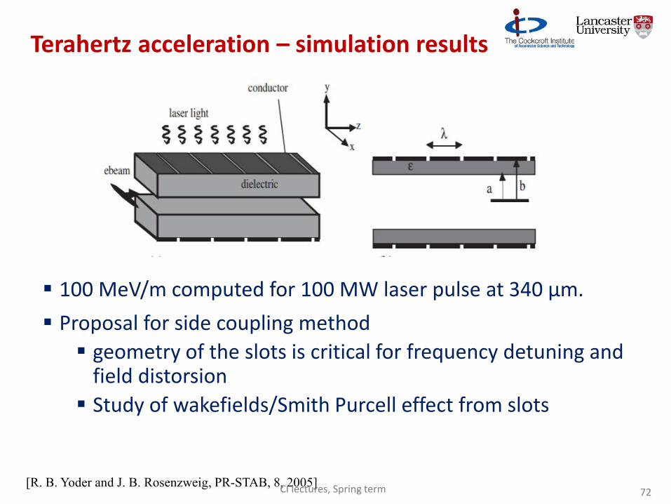
Terahertz acceleration – simulation results
[R. B. Yoder and J. B. Rosenzweig, PR-STAB, 8, 2005]
100 MeV/m computed for 100 MW laser pulse at 340 µm.
Proposal for side coupling method
geometry of the slots is critical for frequency detuning and field distorsion
Study of wakefields/Smith Purcell effect from slots
CI lectures, Spring term 72
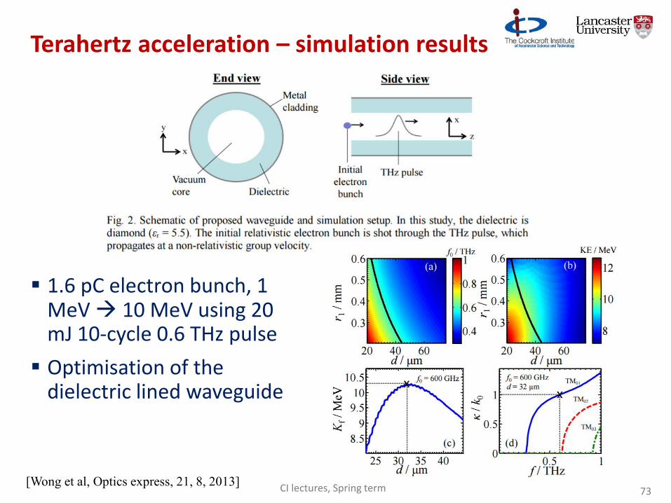
Terahertz acceleration – simulation results
1.6 pC electron bunch, 1 MeV 10 MeV using 20 mJ 10-cycle 0.6 THz pulse
Optimisation of the dielectric lined waveguide
[Wong et al, Optics express, 21, 8, 2013]CI lectures, Spring term 73
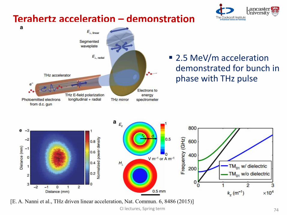
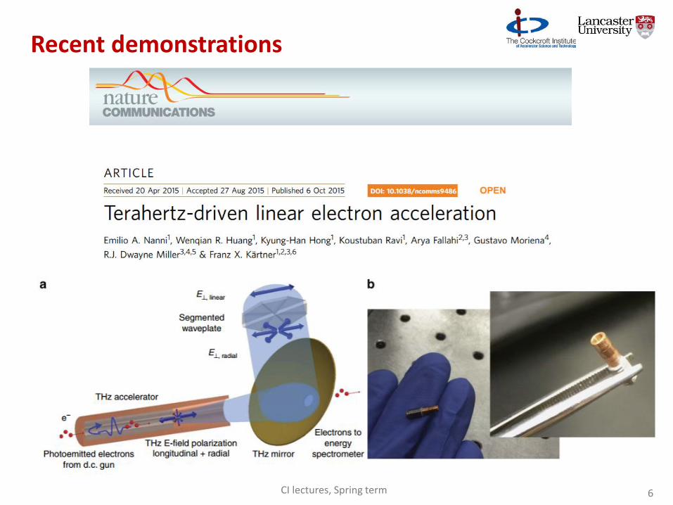
Terahertz acceleration – demonstration
[E. A. Nanni et al., THz driven linear acceleration, Nat. Commun. 6, 8486 (2015)]
2.5 MeV/m acceleration demonstrated for bunch in phase with THz pulse
CI lectures, Spring term 74
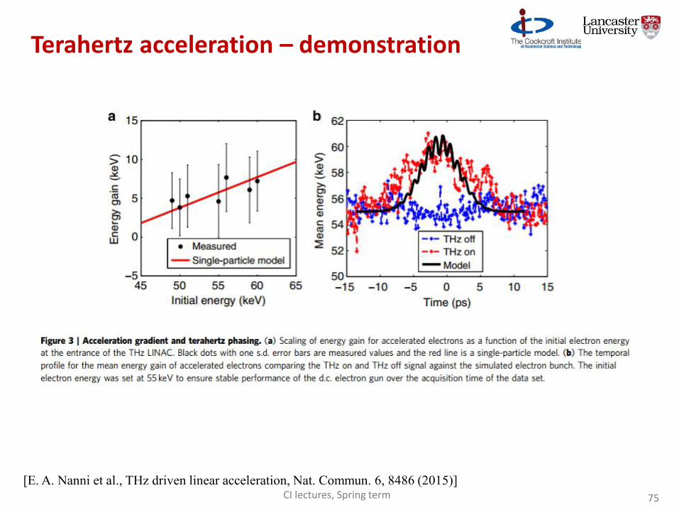
Terahertz acceleration – demonstration
[E. A. Nanni et al., THz driven linear acceleration, Nat. Commun. 6, 8486 (2015)]CI lectures, Spring term 75
Conclusions
High frequency acceleration can provide high gradient, extremely compact and low cost particle accelerators.
Concepts exist from the THz to the optical frequency range.
Structures are mainly all-dielectric and travelling wave based on PhC waveguides.
Proof-of-concept experiments are taking place.
Challenges: low-beta acceleration, power coupling, beam transport, material?, longer wavelength high power laser?, …
CI lectures, Spring term 76