Embed Size (px)
Citation preview

Novel high-k materials
Can we nominate candidates for the 22 and the 16 nm nodes?
Olof EngstromChalmers University of Technology
Paul HurleyTyndall National Institute
Octavian BuiuUniversity of Liverpool
Max LemmeAMO
Outline
• Why high-k?
• Essential properties needed
• Why are rare-earth oxides interesting?
• Comparison between different candidates
• Finalists?
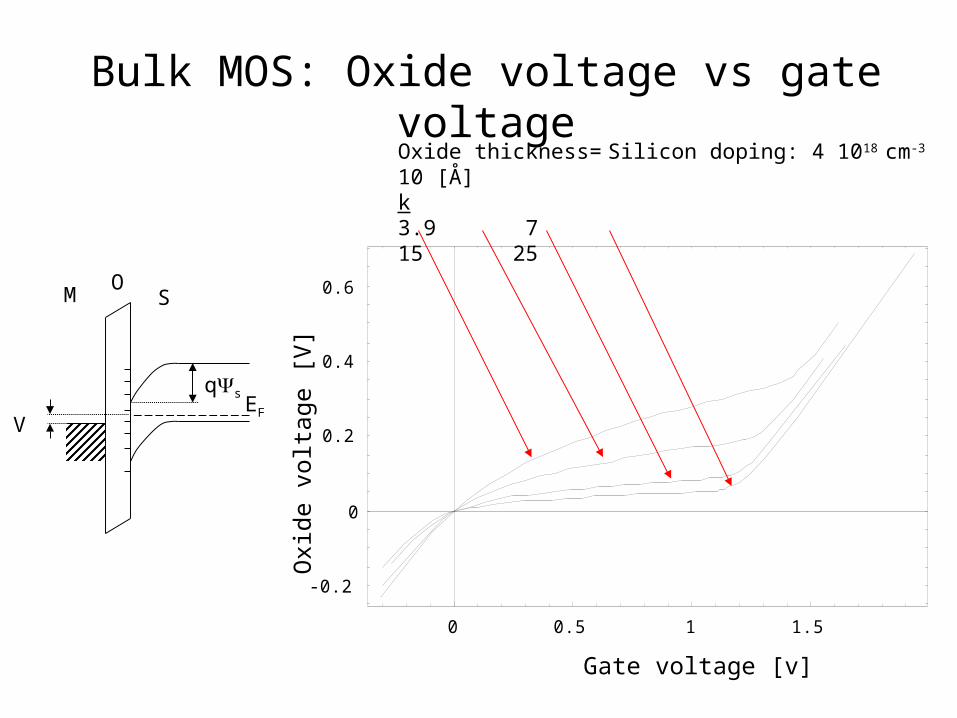
Bulk MOS: Oxide voltage vs gate voltage
0 0.5 1 1.5
-0.2
0
0.2
0.4
0.6
Oxide thickness= 10 [Å]k3.9 7 15 25
Silicon doping: 4 1018 cm-3
Oxi
de v
olta
ge [
V]
Gate voltage [v]
M S
qsEF
V
O

The k-value should be ”lagom”
Mohapatra et al, IEEE Trans. Electron. Dev. 49, 826 (2002)
F
For Lg = 70 nmSiO2
k = 10k = 25
k = 50

Essential properties
Ec
Ev
•k-values•Energy offsets Ec and Ev
•Reactivity with silicon•Hygroscopicity•Structural stability•Interface states•Charge carrier traps
Group**
1 IA 1A
18
VIIIA 8A
1 1 H
1.008
2
IIA 2A
13
IIIA 3A
14
IVA 4A
15
VA 5A
16
VIA 6A
17
VIIA 7A
2 He 4.003
2 3
Li 6.941
4 Be 9.012
5 B
10.81
6 C
12.01
7 N
14.01
8 O
16.00
9 F
19.00
10 Ne 20.18
8 9 10
3 11
Na 22.99
12 Mg 24.31
3
IIIB 3B
4
IVB 4B
5
VB 5B
6
VIB 6B
7
VIIB 7B
------- VIII -------
------- 8 -------
11
IB 1B
12
IIB 2B
13 Al
26.98
14 Si
28.09
15 P
30.97
16 S
32.07
17 Cl 35.45
18 Ar 39.95
4 19 K
39.10
20
Ca 40.08
21 Sc 44.96
22 Ti
47.88
23 V
50.94
24 Cr 52.00
25 Mn 54.94
26 Fe 55.85
27 Co 58.93
28 Ni 58.69
29 Cu 63.55
30 Zn 65.39
31 Ga 69.72
32 Ge 72.59
33 As 74.92
34 Se 78.96
35 Br 79.90
36 Kr 83.80
5 37
Rb 85.47
38 Sr 87.62
39 Y
88.91
40 Zr 91.22
41 Nb 92.91
42 Mo 95.94
43 Tc (98)
44 Ru 101.1
45 Rh 102.9
46 Pd 106.4
47 Ag 107.9
48 Cd 112.4
49 In
114.8
50 Sn 118.7
51 Sb 121.8
52 Te 127.6
53 I
126.9
54 Xe 131.3
6 55
Cs 132.9
56 Ba 137.3
57 La
*138.9
72 Hf 178.5
73 Ta 180.9
74 W
183.9
75 Re 186.2
76 Os 190.2
77 Ir
190.2
78 Pt 195.1
79 Au 197.0
80 Hg 200.5
81 Tl
204.4
82 Pb 207.2
83 Bi 209.0
84 Po (210)
85 At (210)
86 Rn (222)
7 87 Fr (223)
88 Ra (226)
89 Ac ~(227)
104 Rf (257)
105 Db (260)
106 Sg (263)
107 Bh (262)
108 Hs (265)
109 Mt (266)
110 Ds (271)
111 Uuu (272)
112 Uub (277)
114
Uuq (296)
116
Uuh (298)
118
Uuo (?)
Lanthanide Series*
58 Ce 140.1
59 Pr 140.9
60 Nd 144.2
61 Pm (147)
62 Sm 150.4
63 Eu 152.0
64 Gd 157.3
65 Tb 158.9
66 Dy 162.5
67 Ho 164.9
68 Er 167.3
69 Tm 168.9
70 Yb 173.0
71 Lu 175.0
Actinide Series~
90 Th 232.0
91 Pa (231)
92 U
(238)
93 Np (237)
94 Pu (242)
95 Am (243)
96 Cm (247)
97 Bk (247)
98 Cf (249)
99 Es (254)
100 Fm (253)
101 Md (256)
102 No (254)
103 Lr (257)
** Groups are noted by 3 notation conventions.
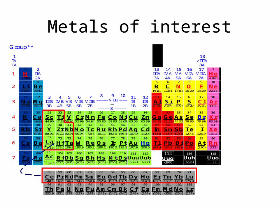
Metals of interest

Polarizability and k-value
]43
11[
]43
21[
mV
mV
k
Clausius-Mosotti
D. G. Schlom et al, Thin films and heterostructures for oxide electronics, (Springer, 2005), p. 31
Si(4+) Al(3+) Hf(4+) Zr(4+) Y(3+) La(3+)Ce(3+)Pr(3+)Gd(3+)Yb(3+)Lu(3+)0
1
2
3
4
5
6
Pol
ariz
abili
ty,
Ion

Energy offset vs. k-value
Borders for the 22 nm LSTP bulk node: 10-2 A/cm2
EOT=0.6 nm Vox= 1V(Target)
Requires k E ≈ 70 eV
O. Engström, B. Raeissi, S. Hall, O. Buiu, M.C. Lemme, H.D.B. Gottlob, P.K. Hurley, K. Cherkaoui, SSE, 51, 622 (2007)
LaLuO3
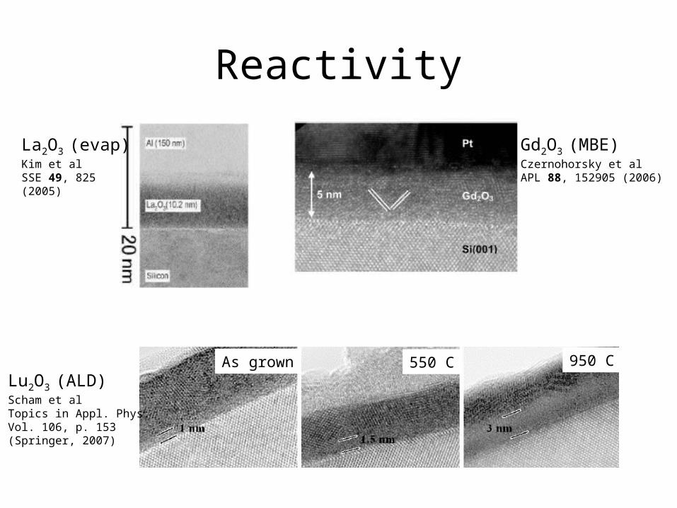
Reactivity
Lu2O3 (ALD)Scham et alTopics in Appl. Phys. Vol. 106, p. 153(Springer, 2007)
La2O3 (evap)Kim et alSSE 49, 825 (2005)
Gd2O3 (MBE)Czernohorsky et alAPL 88, 152905 (2006)
550 C 950 CAs grown

Reactivity
Si + MO
M + SiO2
MSi + SiO2
M + MSiO
G1000C
For Si + O G1000C < 0
G1000C
SiO2
Al2O3 ZrO2 HfO2 Yb2O3 Lu2O3 Gd2O3 Dy2O3Sm2O3 Pr2O3 La2O30
100
200
300
400
500
G [k
J/m
ol]
OxideD. G. Schlom et al, Thin films and heterostructures for oxide electronics, (Springer, 2005), p. 31

Hygroscopicity
SiO2 ZrO2 Yb2O3 Lu2O3 Gd2O3 Dy2O3 Sm2O3 Pr2O3 La2O30,0
0,5
1,0
1,5
2,0
2,5
EO
T (
120
hrs)
/EO
T (
fres
h)Oxide
Eu2O3 ZrO2 Yb2O3 Lu2O3 Gd2O3 Dy2O3 Sm2O3 Pr2O3 La2O31E-3
0,01
0,1
1
10
100
1000
J 12
0 h
rs/J
fre
sh
Oxide
K.Kakushima, K.Tsutsui, S-I. Ohmi, P.Ahmet V.R. Rao and H. Iwai in Rare earth oxide thin films ( Springer, 2007), p. 345
water + oxide hydroxide

Structural stability
APL, 89, 222902 (2006)
Example: LaLuO3

0,4 0,6 0,8 1,0 1,2 1,4 1,61E-9
1E-8
1E-7
1E-6
1E-5
1E-4
1E-3
0,01
0,1
1
Leakage
Gd2O3 [2], HfO2[1], ZrO2[1]
HfGdO [3]
Lu2O3 [4]with epitaxialLu2O3 - silicate IL)
[1] H. Iwai et al, Proc. IEDM, 2002[2] H.D.B. Gottlob et al, IEEE Electron Dev. Lett. 27, 814 (2006)[3] S. Govindarajan et al, APL 91, 062906 (2007)[4] P. Darmawan et al, APL 91, 092903 (2007)[5] A. Ogawa et al Microel. Eng. 84, 1861 (2007)
Le
aka
ge
cu
rre
nt
[A/c
m2]
EOT [nm]
HfO2
andZrO2
3
La2O3 [1]
HfO2 [5](with HfSiO IL)

Experimental C = f (V,freq.)
Gd2O3
ALD
Gd2O3
MBE
B.Raeissi, J.Piscator, O.Engström, S.Hall, O.Buiu, M.C.Lemme, H.D.B.Gottlob, P.Hurley, K.Cerkaoui and H.J.Osten,Proc. ESSDERC, 2007, p 287
HfO2
React.sputt.

LaSiOx/Si interface
-2 -1 0 10.000
0.005
0.010
0.015
0.020
0.025
0.030
1 kHz 10 kHz 100 kHz 1 MHz
Wafer X3361-19 Site 19a18
Ca
pa
cit
an
ce
(F/m
2 )
Voltage Vg (V)
LaSiOx
E-beamevap.
LaSiOx
P.K.Hurley, K.Cherkaoui, E.O’Connor, M.C.Lemme, H. D.B. Gottlob, M.Schmidt , S.Hall, Y.Lu, O.Buiu, B.Raeissi, J. Piscator and O.Engstrom, J. Electrochem. Soc., in press
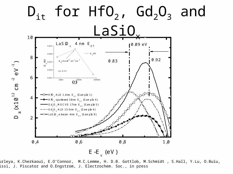
Dit for HfO2, Gd2O3 and LaSiOx
0,4 0,6 0,8 1,0
2
4
6
8
10
10000 100000 10000000.0015
0.0020
0.0025
0.0030
0.0035
Gp/
Gp/
Vg=-0.75V
Dit=5x10¹² eV-1cm-2
HfO2 ALD 1.4nm E
OT (Sample 1)
HfO2 sputtered 18nm E
OT (Sample 4)
Gd2O
3 MOCVD 17nm E
OT (Sample 5)
Gd2O
3 ALD 13.5nm E
OT (Sample 6)
LaSiOx e-beam 4nm E
OT (Sample 9)
Dit (x
1012
cm
-2 e
V-1)
E-Ev (eV)
0.83 0.92
0.09 eVLaSiOx 4 nm E
OT
P.K.Hurleya, K.Cherkaoui, E.O’Connor, M.C.Lemme, H. D.B. Gottlob, M.Schmidt , S.Hall, Y.Lu, O.Buiu, B.Raeissi, J. Piscator and O.Engstrom, J. Electrochem. Soc., in press
Group**
1 IA 1A
18
VIIIA 8A
1 1 H
1.008
2
IIA 2A
13
IIIA 3A
14
IVA 4A
15
VA 5A
16
VIA 6A
17
VIIA 7A
2 He 4.003
2 3
Li 6.941
4 Be 9.012
5 B
10.81
6 C
12.01
7 N
14.01
8 O
16.00
9 F
19.00
10 Ne 20.18
8 9 10
3 11
Na 22.99
12 Mg 24.31
3
IIIB 3B
4
IVB 4B
5
VB 5B
6
VIB 6B
7
VIIB 7B
------- VIII -------
------- 8 -------
11
IB 1B
12
IIB 2B
13 Al
26.98
14 Si
28.09
15 P
30.97
16 S
32.07
17 Cl 35.45
18 Ar 39.95
4 19 K
39.10
20
Ca 40.08
21 Sc 44.96
22 Ti
47.88
23 V
50.94
24 Cr 52.00
25 Mn 54.94
26 Fe 55.85
27 Co 58.93
28 Ni 58.69
29 Cu 63.55
30 Zn 65.39
31 Ga 69.72
32 Ge 72.59
33 As 74.92
34 Se 78.96
35 Br 79.90
36 Kr 83.80
5 37
Rb 85.47
38 Sr 87.62
39 Y
88.91
40 Zr 91.22
41 Nb 92.91
42 Mo 95.94
43 Tc (98)
44 Ru 101.1
45 Rh 102.9
46 Pd 106.4
47 Ag 107.9
48 Cd 112.4
49 In
114.8
50 Sn 118.7
51 Sb 121.8
52 Te 127.6
53 I
126.9
54 Xe 131.3
6 55
Cs 132.9
56 Ba 137.3
57 La
*138.9
72 Hf 178.5
73 Ta 180.9
74 W
183.9
75 Re 186.2
76 Os 190.2
77 Ir
190.2
78 Pt 195.1
79 Au 197.0
80 Hg 200.5
81 Tl
204.4
82 Pb 207.2
83 Bi 209.0
84 Po (210)
85 At (210)
86 Rn (222)
7 87 Fr (223)
88 Ra (226)
89 Ac ~(227)
104 Rf (257)
105 Db (260)
106 Sg (263)
107 Bh (262)
108 Hs (265)
109 Mt (266)
110 Ds (271)
111 Uuu (272)
112 Uub (277)
114
Uuq (296)
116
Uuh (298)
118
Uuo (?)
Lanthanide Series*
58 Ce 140.1
59 Pr 140.9
60 Nd 144.2
61 Pm (147)
62 Sm 150.4
63 Eu 152.0
64 Gd 157.3
65 Tb 158.9
66 Dy 162.5
67 Ho 164.9
68 Er 167.3
69 Tm 168.9
70 Yb 173.0
71 Lu 175.0
Actinide Series~
90 Th 232.0
91 Pa (231)
92 U
(238)
93 Np (237)
94 Pu (242)
95 Am (243)
96 Cm (247)
97 Bk (247)
98 Cf (249)
99 Es (254)
100 Fm (253)
101 Md (256)
102 No (254)
103 Lr (257)
** Groups are noted by 3 notation conventions.
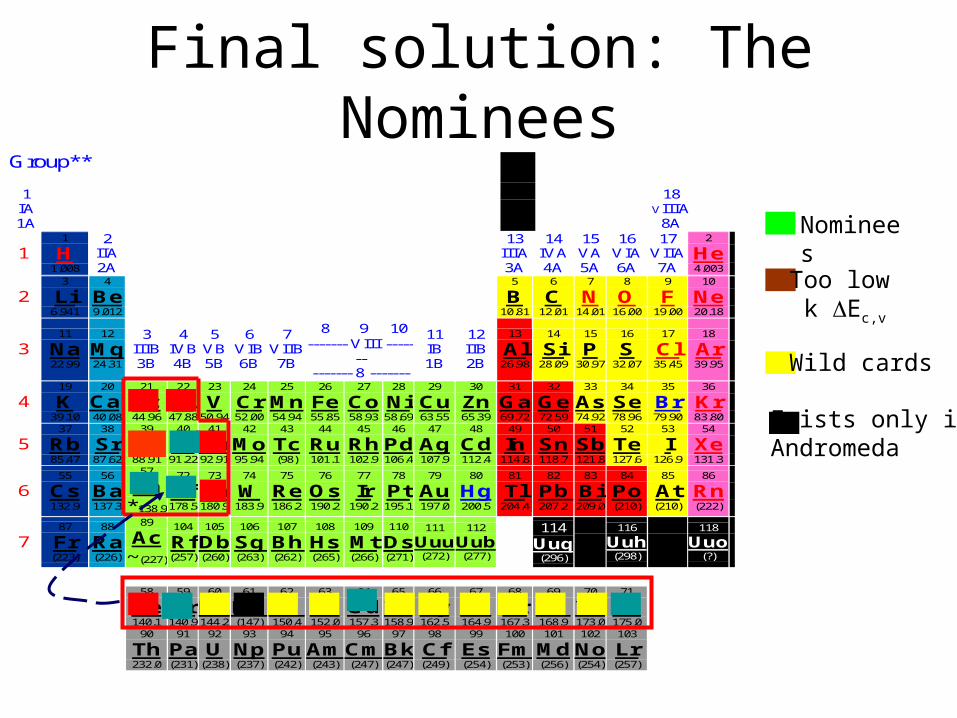
Final solution: The Nominees
Nominees
Too low k Ec,v
Wild cards
Exists only in Andromeda

Finalists
Pr2O3 La2O3 Gd2O3 LaLuO3 HfO2 ZrO2
k x DEc 66 69 42 67 35 38
k x DEv Low 66 31 67 83 80
Reactivity High High Low High High High
Hygroscop. Low High High Low Low Low
Struct. stab. Low Low High High Low Low

Conclusion
there is a lot more work to do!
Lantanum based oxides seem worth a bid
but fortunately for academic people
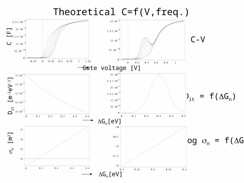
Theoretical C=f(V,freq.)
C-V
Dit = f(Gn)
log n = f(Gn)
-0.25 0 0.25 0.5 0.75 1 1.250
5 10-10
1 10-9
1.5 10-9
2 10-9
2.5 10-9
0 0.1 0.2 0.3 0.4 0.5
3 1017
4 1017
5 1017
6 1017
7 1017
0 0.1 0.2 0.3 0.4
-24
-23
-22
-21
0 0.1 0.2 0.3 0.4 0.50
5 1016
1 1017
1.5 1017
2 1017
2.5 1017
3 1017
0.2 0.25 0.3 0.35 0.4
-22
-21.5
-21
-20.5
-20
0 0.2 0.4 0.6 0.8 10
5 10-10
1 10-9
1.5 10-9
2 10-9
C [
F]
Gate voltage [V]
Gn[eV]
Gn[eV]
Dit
[m-2eV
-1]
n [
m2 ]
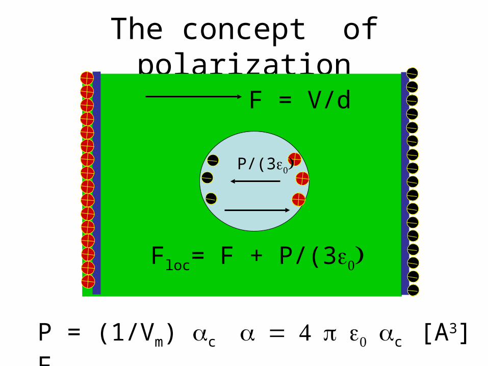
The concept of polarization
F = V/d
P/(3
Floc= F + P/(3
P = (1/Vm) c Floc c [A3]
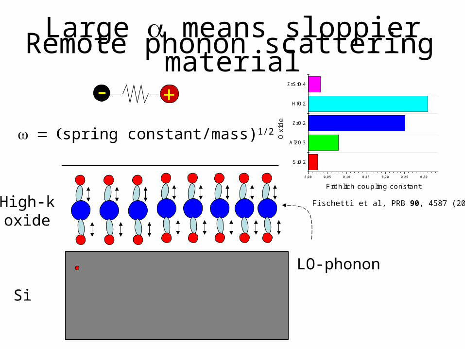
Large means sloppier material
+-
spring constant/mass)1/2
Si
High-koxide
LO-phonon
Remote phonon scattering
Fischetti et al, PRB 90, 4587 (2001)
SiO2
Al2O3
ZrO2
HfO2
ZrSiO4
0,00 0,05 0,10 0,15 0,20 0,25 0,30
Fröhlich coupling constant
Oxi
de