Embed Size (px)
Citation preview
1
ASP-DAC 2014
1
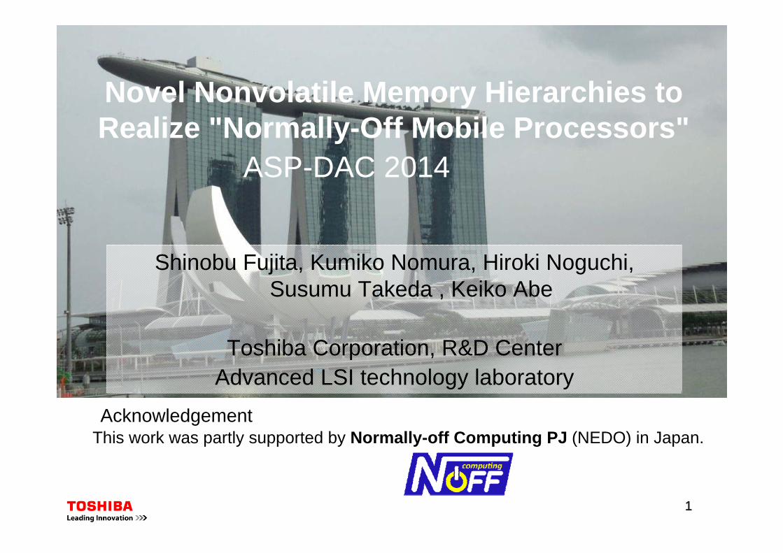
Novel Nonvolatile Memory Hierarchies to Realize "Normally-Off Mobile Processors"
Shinobu Fujita, Kumiko Nomura, Hiroki Noguchi, Susumu Takeda , Keiko Abe
Toshiba Corporation, R&D CenterAdvanced LSI technology laboratory
This work was partly supported by Normally-off Computing PJ (NEDO) in Japan.Acknowledgement
2
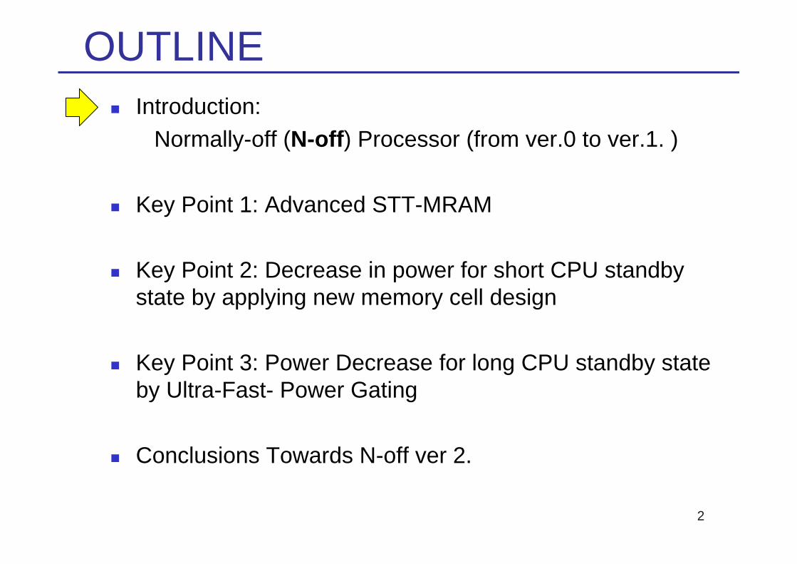
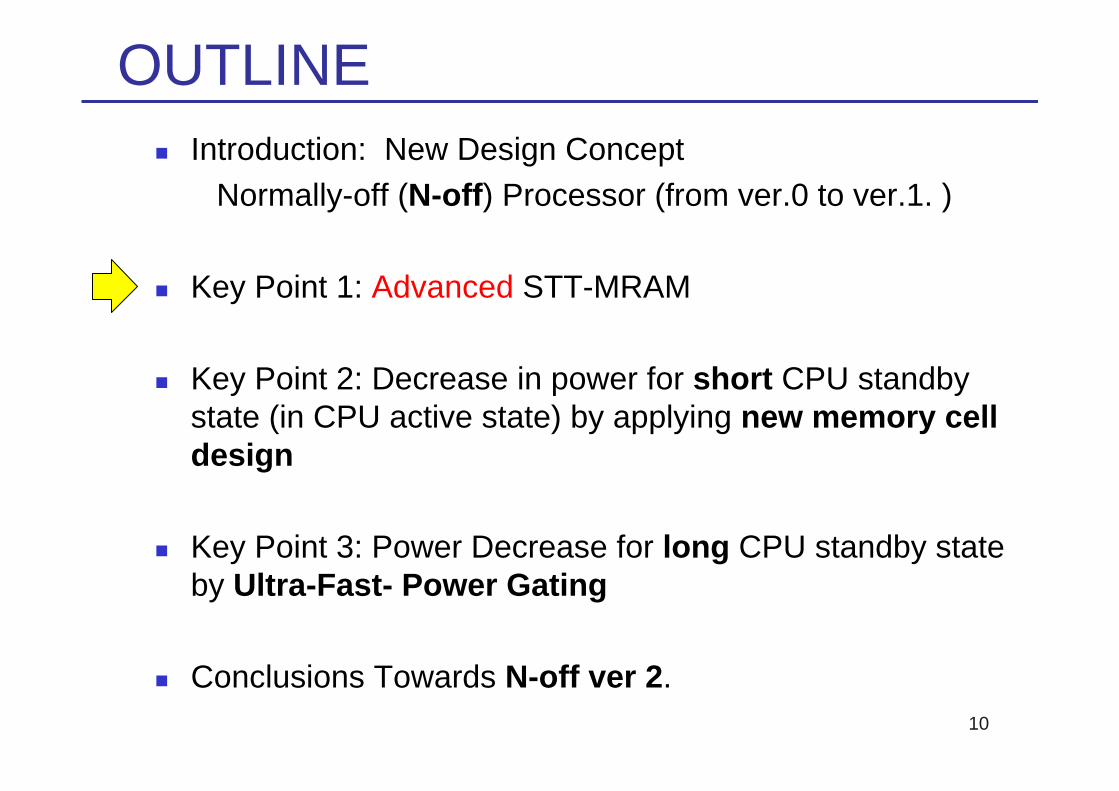
OUTLINE Introduction:
Normally-off (N-off) Processor (from ver.0 to ver.1. )
Key Point 1: Advanced STT-MRAM
Key Point 2: Decrease in power for short CPU standby state by applying new memory cell design
Key Point 3: Power Decrease for long CPU standby state by Ultra-Fast- Power Gating
Conclusions Towards N-off ver 2.
3
Normally-Off Computer Ver.0 (2001)(FED journal Japan, 2001)
volatileNon-
VolatileMemory(MRAM)
Register files
ALU/FlipFlop
Cache (L2)
Main memory
Storage
Cache (L1)
non-volatile
Memory Hierarchy
Proposed by K. Ando, AIST, Japan
History of Concept on Normally-Off Computer
The same Ver.0 concept presented by T. Kawahara, ASP-DAC 2011.
(based on MRAM)
volatileVolatileMemory Register files
ALU/FlipFlop
Cache (L2)
Main memory
Storage
Cache (L1)
non-volatile
Memory Hierarchy
“Nonvolatile memoryand normally-off computing”
4
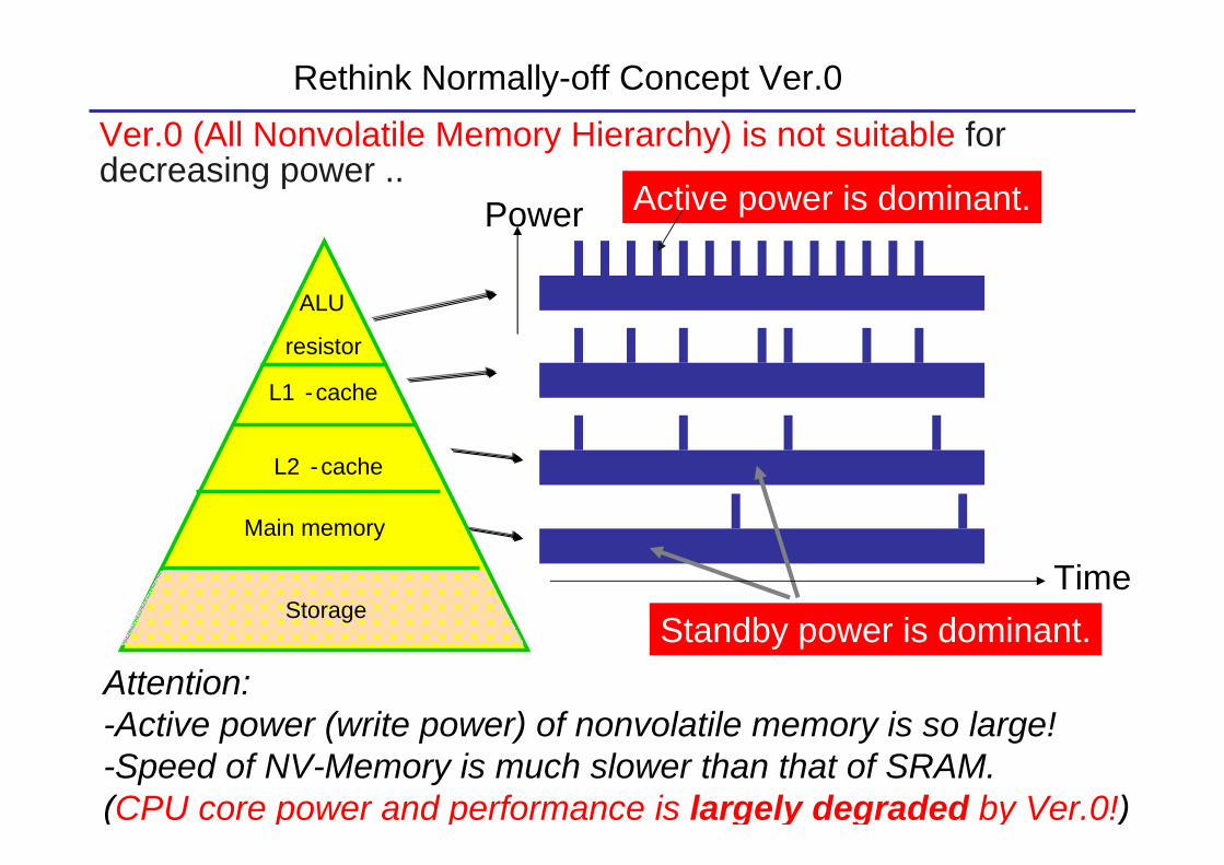
Attention: -Active power (write power) of nonvolatile memory is so large! -Speed of NV-Memory is much slower than that of SRAM.(CPU core power and performance is largely degraded by Ver.0!)
L2 -cache
resistor
Main memory
L1 -cache
ALU
Storage
Active power is dominant.
Standby power is dominant.
Ver.0 (All Nonvolatile Memory Hierarchy) is not suitable for decreasing power ..
Power
Time
Rethink Normally-off Concept Ver.0
5
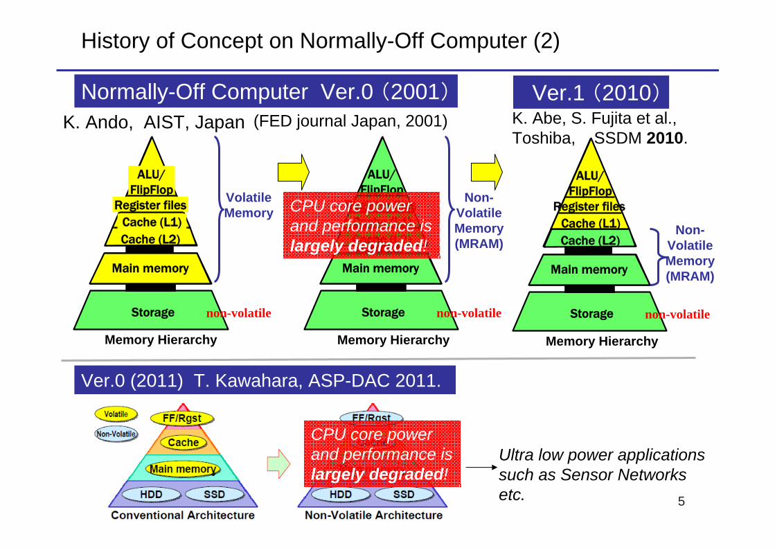
Normally-Off Computer Ver.0 (2001)(FED journal Japan, 2001)
volatileNon-
VolatileMemory(MRAM)
Register files
ALU/FlipFlop
Cache (L2)
Main memory
Storage
Cache (L1)
non-volatile
Memory Hierarchy
K. Ando, AIST, Japan
History of Concept on Normally-Off Computer (2)
Ver.0 (2011) T. Kawahara, ASP-DAC 2011.
volatileVolatileMemory Register files
ALU/FlipFlop
Cache (L2)
Main memory
Storage
Cache (L1)
non-volatile
Memory Hierarchy
K. Abe, S. Fujita et al., Toshiba, SSDM 2010.
Non-VolatileMemory(MRAM)
Register files
ALU/FlipFlop
Cache (L2)
Main memory
Storage
Cache (L1)
non-volatile
Memory Hierarchy
CPU core power and performance is largely degraded!
Ver.1 (2010)
CPU core power and performance is largely degraded!
Ultra low power applicationssuch as Sensor Networks etc.
6
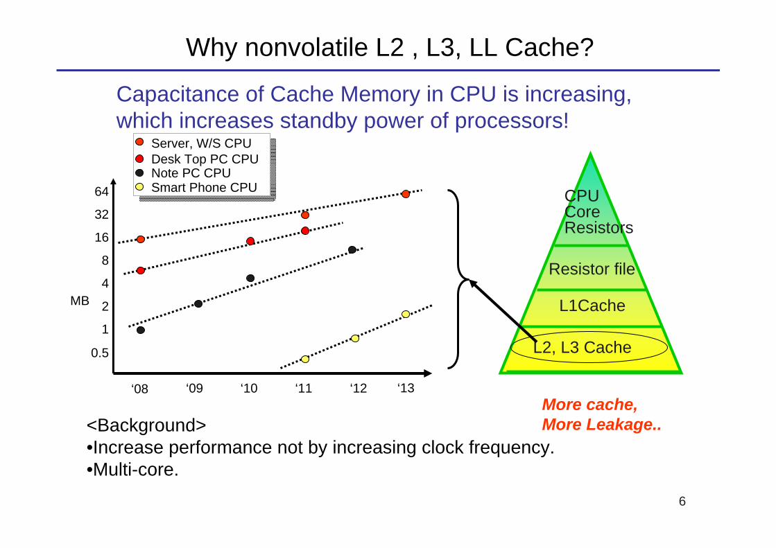
Capacitance of Cache Memory in CPU is increasing, which increases standby power of processors!
<Background>•Increase performance not by increasing clock frequency.•Multi-core.
‘08 ‘09 ‘10 ‘11 ‘12 ‘13
MB
Server, W/S CPU
2
4
8
16
32
1
64 Smart Phone CPU
0.5
Note PC CPUDesk Top PC CPU
CPU CoreResistors
L2, L3 Cache
Resistor file
L1Cache
More cache,More Leakage..
Why nonvolatile L2 , L3, LL Cache?
7
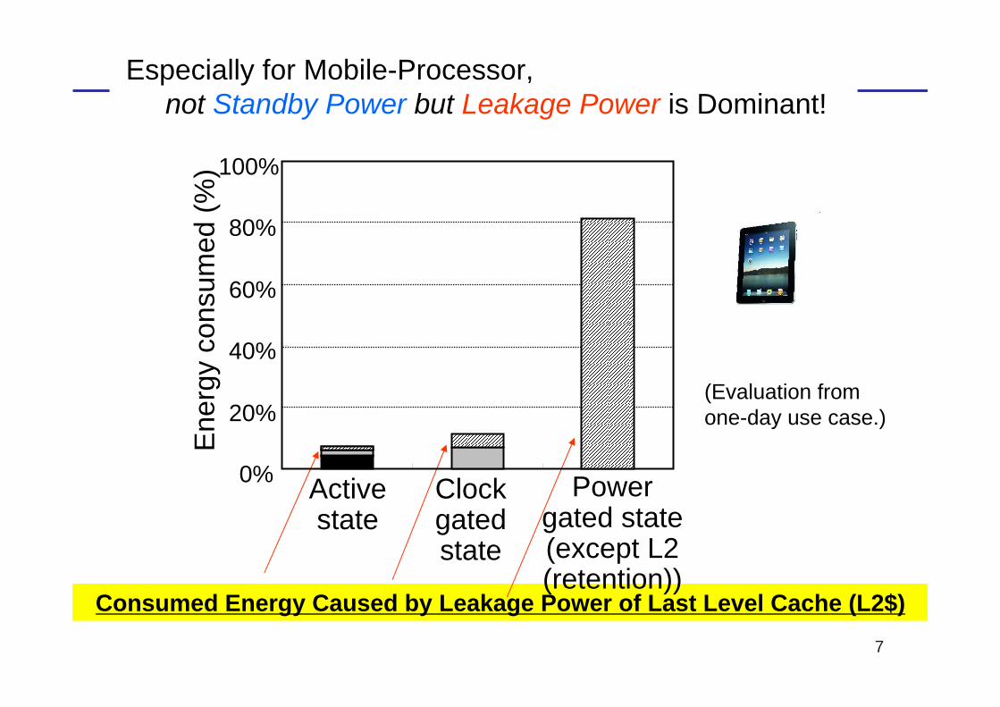
Consumed Energy Caused by Leakage Power of Last Level Cache (L2$)
Especially for Mobile-Processor, not Standby Power but Leakage Power is Dominant!
(Evaluation from one-day use case.)
0%
20%
40%
60%
80%
100%
Activestate
Clockgatedstate
Powergated state(except L2 (retention))
Ene
rgy
cons
umed
(%)
8
1
10
100
1000
Acc
ess
spe
ed (
ns)
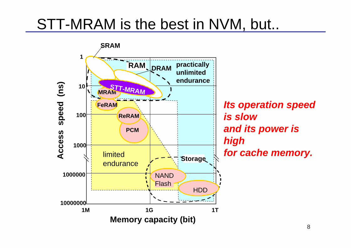
limitedendurance
RAM
Storage
Memory capacity (bit)1M 1G 1T
HDD
1000000
PCM
FeRAM
MRAM
10000000
practicallyunlimitedendurance
SRAM
NANDFlash
DRAM
STT-MRAM
ReRAM
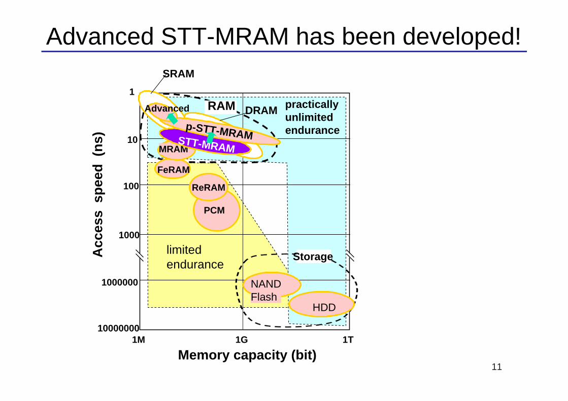
STT-MRAM is the best in NVM, but..
Its operation speed is slowand its power is high for cache memory.
9
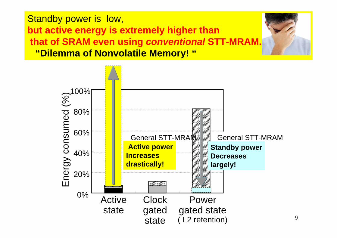
0%
20%
40%
60%
80%
100%
Activestate
Clockgatedstate
Powergated state( L2 retention)
Ene
rgy
cons
umed
(%)
General STT-MRAMActive powerIncreasesdrastically!
Standby power is low, but active energy is extremely higher than that of SRAM even using conventional STT-MRAM.“Dilemma of Nonvolatile Memory! “
General STT-MRAMStandby powerDecreaseslargely!
10
OUTLINE Introduction: New Design Concept
Normally-off (N-off) Processor (from ver.0 to ver.1. )
Key Point 1: Advanced STT-MRAM
Key Point 2: Decrease in power for short CPU standby state (in CPU active state) by applying new memory cell design
Key Point 3: Power Decrease for long CPU standby state by Ultra-Fast- Power Gating
Conclusions Towards N-off ver 2.
11
1
10
100
1000
Acc
ess
spe
ed (
ns)
limitedendurance
RAM
Storage
Memory capacity (bit)1M 1G 1T
HDD
1000000
PCM
FeRAM
MRAM
10000000
practicallyunlimitedendurance
SRAM
NANDFlash
DRAM
STT-MRAM
ReRAM
p-STT-MRAM
Advanced
Advanced STT-MRAM has been developed!
12
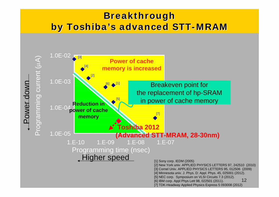
Breakthrough Breakthrough by Toshibaby Toshiba’’s advanced STTs advanced STT--MRAMMRAM
1.0E-05
1.0E-04
1.0E-03
1.0E-02
1.E-10 1.E-09 1.E-08 1.E-07Programming time (nsec)
Pro
gram
min
g cu
rrent
(A
)
Breakeven point for the replacement of hp-SRAM
in power of cache memory
[1] Sony corp. IEDM (2005)[2] New York univ. APPLIED PHYSICS LETTERS 97, 242510 (2010) [3] Cornel Univ. APPLIED PHYSICS LETTERS 95, 012506 (2009) [4] Minnesota univ. J. Phys. D: Appl. Phys. 45, 025001 (2012).[5] NEC corp. Symposium on VLSI Circuits 7.3 (2012).[6] IBM corp. Appl Phys Lett 98, 022501 (2011).[7] TDK-Headway Applied Physics Express 5 093008 (2012)
[3]
[1]
[2]
[4]
[5]
[6]
[7]
Power of cache memory is increased
Reduction in power of cache
memory
Toshiba 2012(Advanced STT-MRAM, 28-30nm)
Pow
er d
own
Higher speed
13
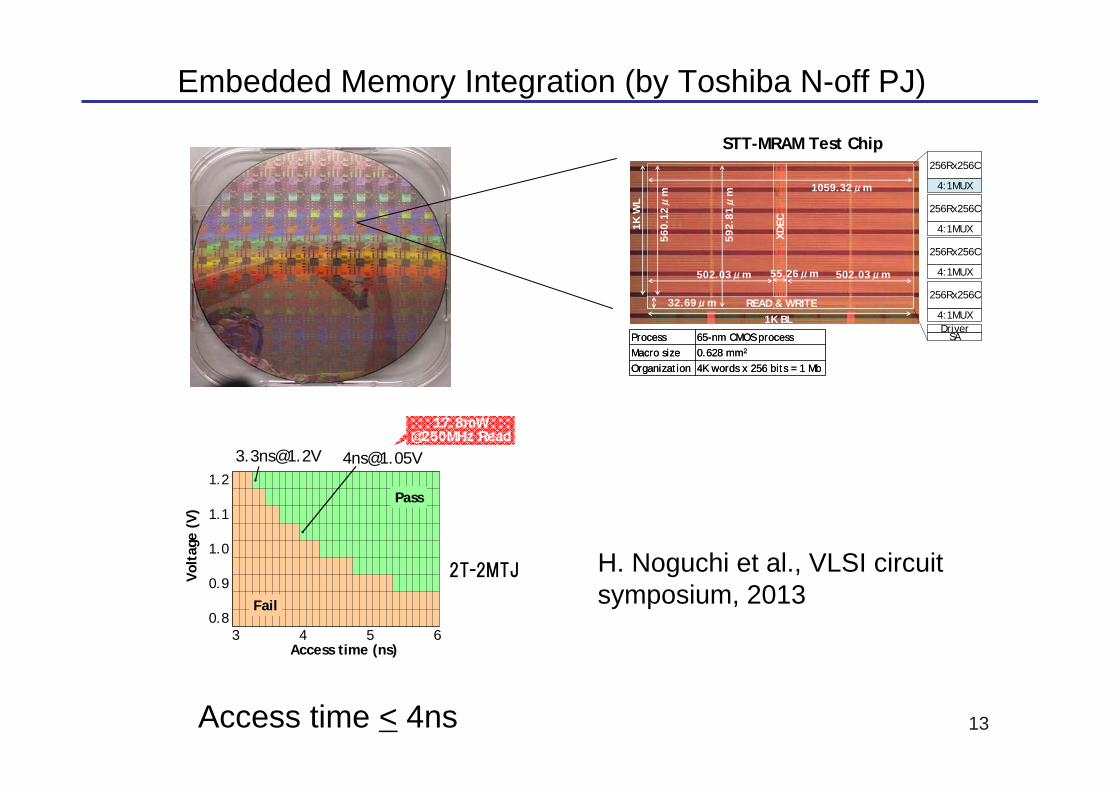
Access Time Measurements
Volt
age
(V)
Access time (ns)
Pass
Fail
1.2
1.1
1.0
0.9
0.83 4 5 6
[email protected] [email protected]
17.8mW@250MHz Read
STT-MRAM Test Chip
502.03μm 502.03μm55.26μm
560.
12μ
m
32.69μm
592.
81μ
m 1059.32μm
XDEC
READ & WRITE1K BL
1K W
L
4:1MUX
256Rx256C
4:1MUX
256Rx256C
4:1MUX
256Rx256C
4:1MUX
256Rx256C
DriverSAProcess 65-nm CMOS process
Macro size 0.628 mm2
Organization 4K words x 256 bits = 1 Mb
Process 65-nm CMOS processMacro size 0.628 mm2
Organization 4K words x 256 bits = 1 Mb
2T-2MTJ
Embedded Memory Integration (by Toshiba N-off PJ)
Access time < 4ns
H. Noguchi et al., VLSI circuit symposium, 2013
14
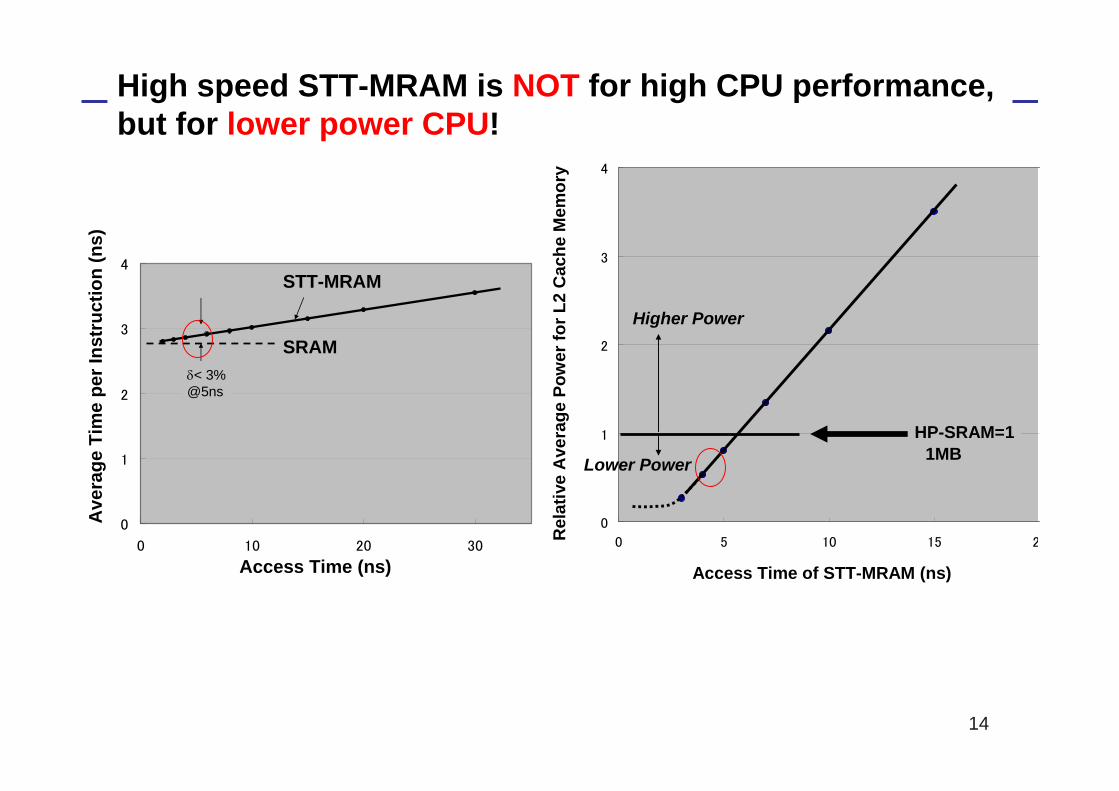
High speed STT-MRAM is NOT for high CPU performance, but for lower power CPU!
0
1
2
3
4
0 10 20 30
SRAM
Access Time (ns)
Ave
rage
Tim
e pe
r Ins
truc
tion
(ns)
STT-MRAM
< 3%@5ns
0
1
2
3
4
0 5 10 15 2Rel
ativ
e A
vera
ge P
ower
for L
2 C
ache
Mem
ory
Access Time of STT-MRAM (ns)
HP-SRAM=1
Higher Power
Lower Power 1MB
15
CMOS
配線層
CMOS
STT-MRAM
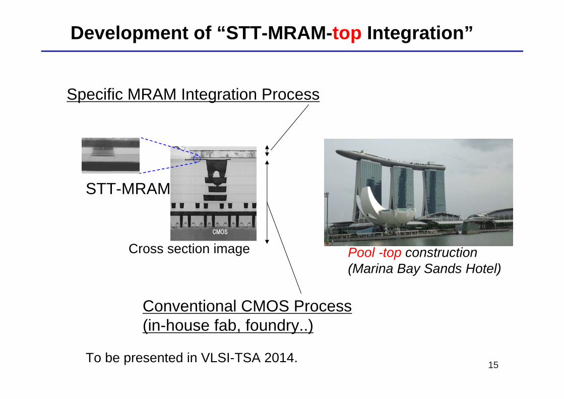
Development of “STT-MRAM-top Integration”
Cross section image
Conventional CMOS Process(in-house fab, foundry..)
Specific MRAM Integration Process
Pool -top construction (Marina Bay Sands Hotel)
To be presented in VLSI-TSA 2014.
16
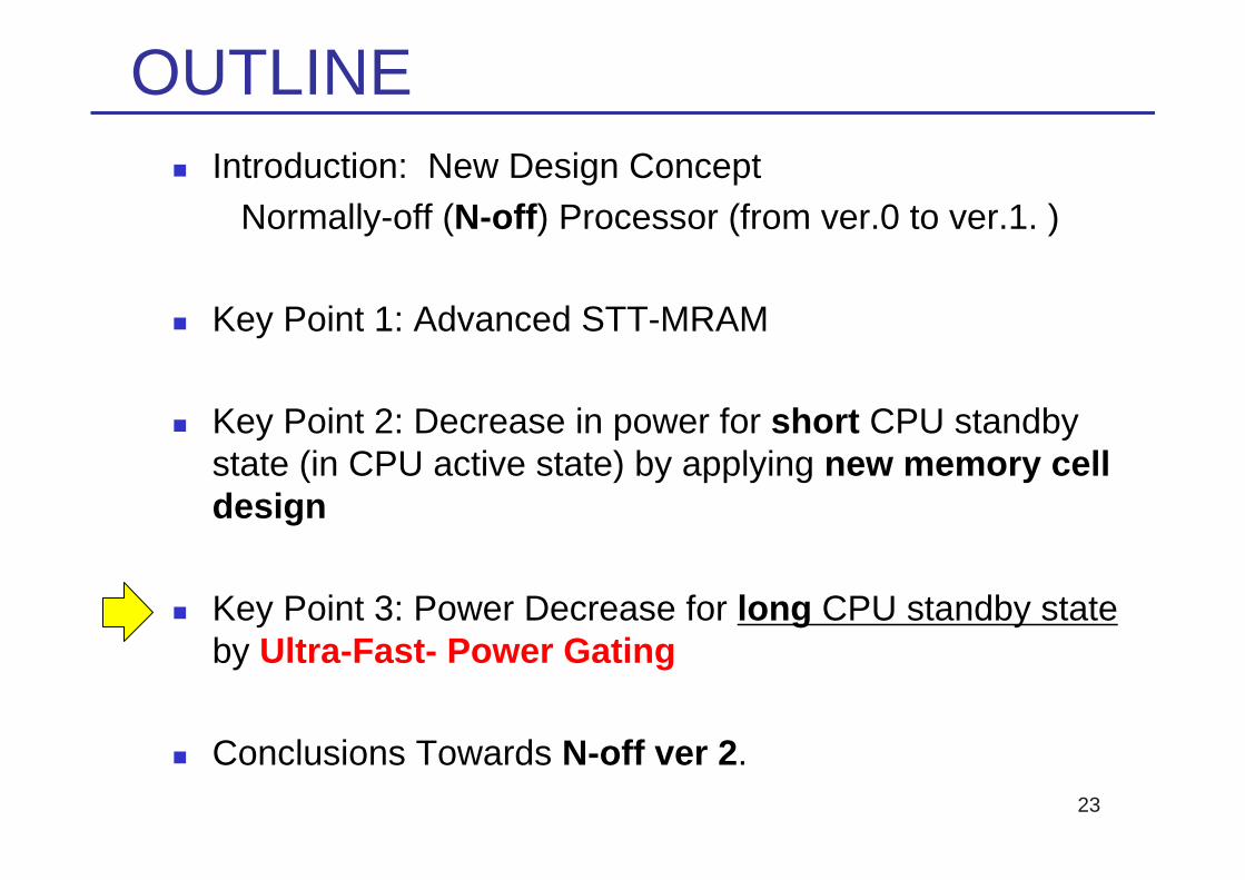
OUTLINE Introduction: New Design Concept
Normally-off (N-off) Processor (from ver.0 to ver.1. )
Key Point 1: Advanced STT-MRAM
Key Point 2: Decrease in power for short CPU standby state (in CPU active state) by applying new memory cell design (normally-off type design)
Key Point 3: Power Decrease for long CPU standby state by Ultra-Fast- Power Gating
Conclusions Towards N-off ver 2.
17
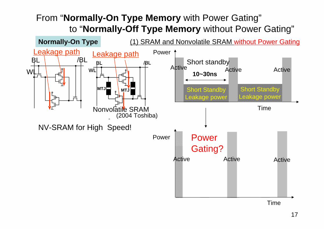
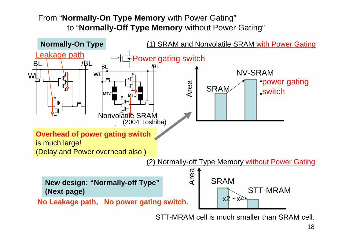
Short StandbyLeakage power
From “Normally-On Type Memory with Power Gating”to “Normally-Off Type Memory without Power Gating”
(1) SRAM and Nonvolatile SRAM without Power Gating
Time
Power
Short StandbyLeakage power
10~30ns
Power
Time
WL
BL /BLLeakage path
Active Active Active
Active Active Active
Leakage path
Nonvolatile SRAM
WLBL /BL
FP
PF
WLBL /BL
FP
PF
- (2004 Toshiba)
MTJ MTJ
Normally-On Type
NV-SRAM for High Speed!PowerGating?
Short standby
18
From “Normally-On Type Memory with Power Gating”to “Normally-Off Type Memory without Power Gating”
(1) SRAM and Nonvolatile SRAM with Power Gating
(2) Normally-off Type Memory without Power Gating
WL
BL /BLLeakage path
No Leakage path, No power gating switch.
Nonvolatile SRAM
WLBL /BL
FP
PF
WLBL /BL
FP
PF
- (2004 Toshiba)
MTJ MTJ
New design: “Normally-off Type”(Next page)
Normally-On Type
Overhead of power gating switchis much large! (Delay and Power overhead also )
Power gating switch
SRAM
NV-SRAM
Are
aSRAM
x2 ~x4A
rea
power gatingswitch
STT-MRAM
STT-MRAM cell is much smaller than SRAM cell.
19
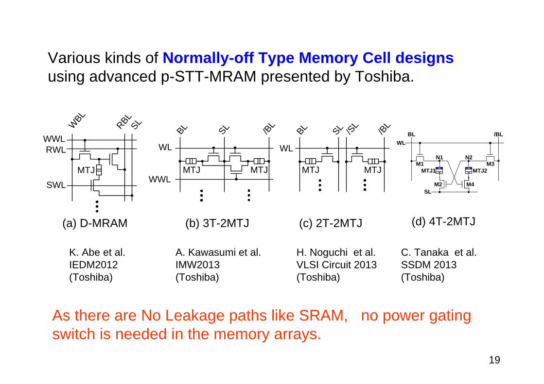
(a) D-MRAM (b) 3T-2MTJ (c) 2T-2MTJ
WBL
SLRWL
WWL
SWL
RBL
MTJ
WL
BL SL /BL
WWLMTJ MTJ
WL
BL SL /BL
/SL
MTJ MTJ
K. Abe et al.IEDM2012(Toshiba)
A. Kawasumi et al.IMW2013(Toshiba)
H. Noguchi et al.VLSI Circuit 2013(Toshiba)
(d) 4T-2MTJ
C. Tanaka et al.SSDM 2013(Toshiba)
Various kinds of Normally-off Type Memory Cell designsusing advanced p-STT-MRAM presented by Toshiba.
As there are No Leakage paths like SRAM, no power gating switch is needed in the memory arrays.
MTJ1
WLBL /BL
SL
M1
M2
N1M3
M4
N2
PF
PF
PF
PF MTJ2
20
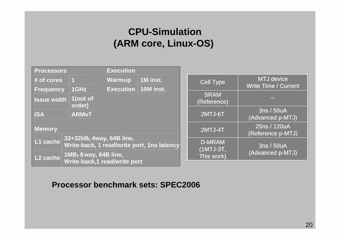
Processors# of cores 1Frequency 1GHz
Issue width 1(out of order)
ISA ARMv7
Memory
L1 cache 32+32kB, 4- way, 64B line, Write-back, 1 read/write port, 1ns latency
L2 cache 1MB, 8- way, 64B line,
-
-Write-back,1 read/write port
ExecutionWarm-up 1M inst.Execution 10M inst.
-
--SRAM(Reference)
3ns / 50uA(Advanced p-MTJ)2MTJ-6T
25ns / 120uA(Reference p-MTJ)2MTJ-4T
3ns / 50uA(Advanced p-MTJ)
MTJ deviceWrite Time / Current
D-MRAM(1MTJ-3T, This work)
Cell Type
--SRAM(Reference)
3ns / 50uA(Advanced p-MTJ)2MTJ-6T
25ns / 120uA(Reference p-MTJ)2MTJ-4T
3ns / 50uA(Advanced p-MTJ)
MTJ deviceWrite Time / Current
D-MRAM(1MTJ-3T, This work)
Cell Type
CPU-Simulation(ARM core, Linux-OS)
Processor benchmark sets: SPEC2006
21
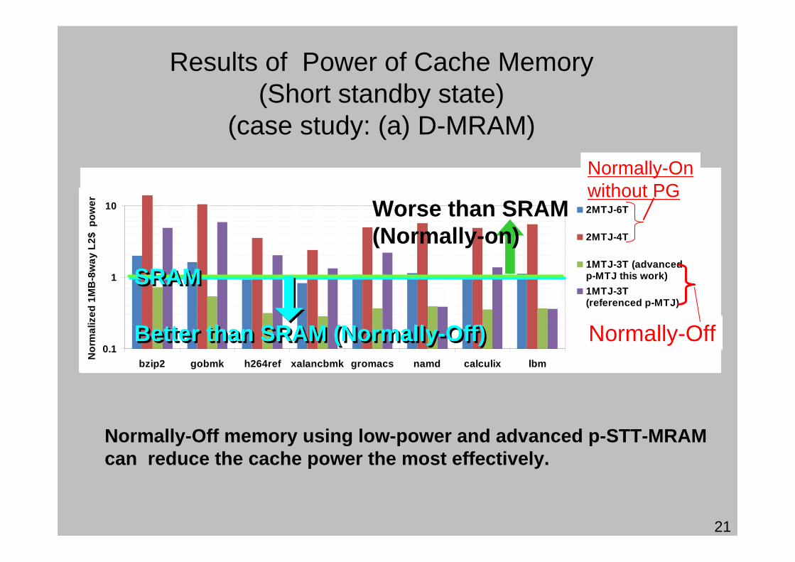
Results of Power of Cache Memory(Short standby state)
(case study: (a) D-MRAM)
0.1
1
10
bzip2 gobmk h264ref xalancbmk gromacs namd calculix lbm
Nor
mal
ized
1M
B-8
way
L2$
pow
er 2MTJ-6T
2MTJ-4T
1MTJ-3T (advancedp-MTJ this work)1MTJ-3T(referenced p-MTJ)
Normally-Off
Normally-Onwithout PG
Normally-Off memory using low-power and advanced p-STT-MRAM can reduce the cache power the most effectively.
Worse than SRAM(Normally-on)
SRAMSRAM
Better than SRAM (Normally-Off)Better than SRAM (Normally-Off)
22
0
0.2
0.4
0.6
0.8
1
bzip2 gobmk h264ref xalancbmk gromacs namd calculix lbm
Nor
mal
ized
inst
ruct
ions
per
cyc
les
(IPC
) (a
. u.)
2MTJ-6T
2MTJ-4T
1MTJ-3T (advancedp-MTJ this work)1MTJ-3T (referencedp-MTJ)
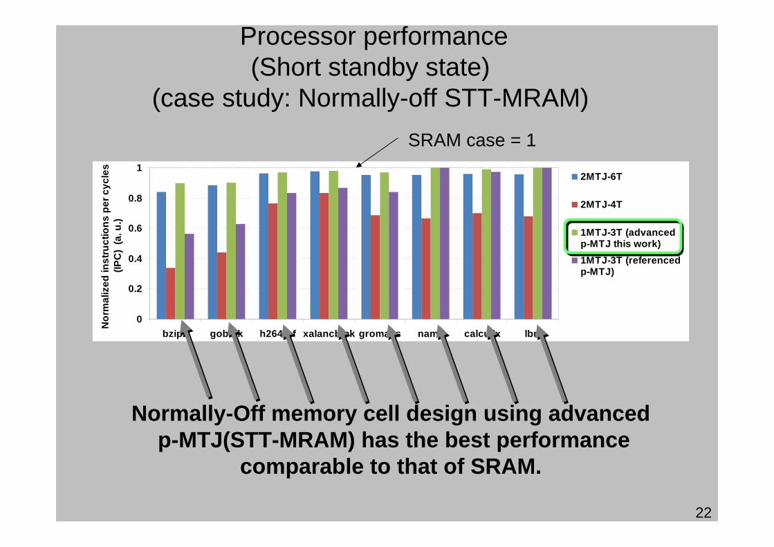
Normally-Off memory cell design using advancedp-MTJ(STT-MRAM) has the best performance
comparable to that of SRAM.
Processor performance(Short standby state)
(case study: Normally-off STT-MRAM) SRAM case = 1
23
OUTLINE Introduction: New Design Concept
Normally-off (N-off) Processor (from ver.0 to ver.1. )
Key Point 1: Advanced STT-MRAM
Key Point 2: Decrease in power for short CPU standby state (in CPU active state) by applying new memory cell design
Key Point 3: Power Decrease for long CPU standby stateby Ultra-Fast- Power Gating
Conclusions Towards N-off ver 2.
24
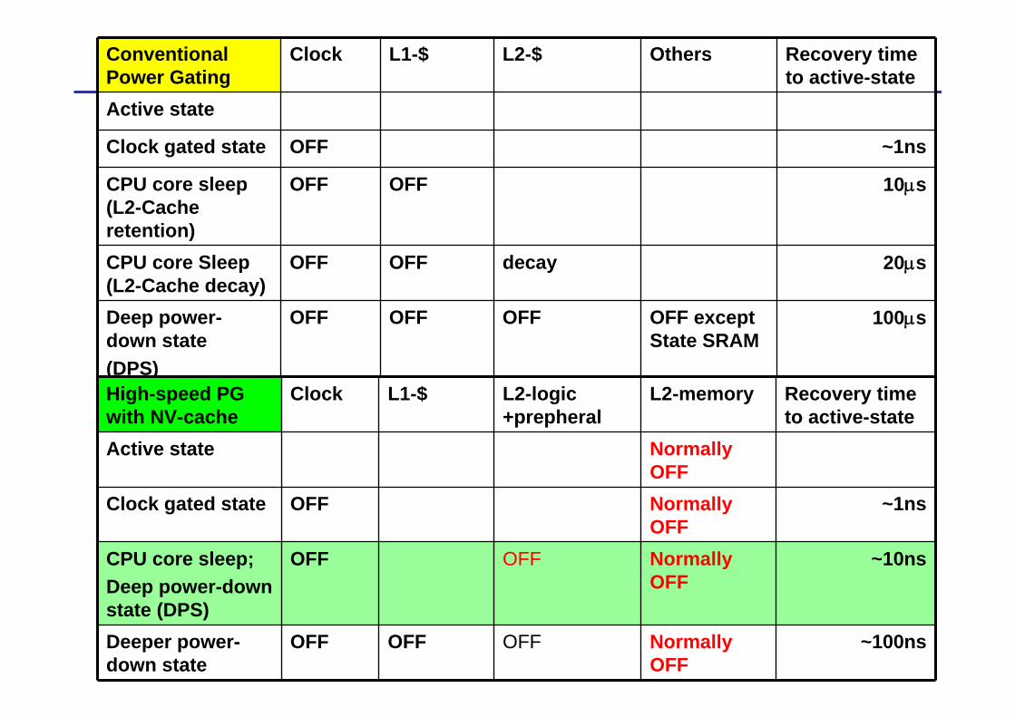
Recovery time to active-state
OthersL2-$L1-$ClockConventional Power GatingActive state
Clock gated state OFF ~1ns
CPU core sleep (L2-Cache retention)
OFF OFF 10s
CPU core Sleep (L2-Cache decay)
OFF OFF decay 20s
Deep power-down state(DPS)
OFF OFF OFF OFF except State SRAM
100s
~100nsNormally OFF
OFFOFFOFFDeeper power-down state
OFF
L2-logic +prepheral
Recovery time to active-state
L2-memoryL1-$ClockHigh-speed PG with NV-cacheActive state Normally
OFFClock gated state OFF Normally
OFF~1ns
CPU core sleep;Deep power-down state (DPS)
OFF Normally OFF
~10ns
25
Power(%)
Active state
CPU core sleep state
Deep power-down state (DPS)
Clock gated
1
20sec
20nsecIdle time
(ns)
0
100
50
10 102 103 104 105 106
Clock gated
L2 cache decay
2nsec
40sec
200sec
Deep power-down state (DPS)
Conventional PG
Ultra-fast PG + Nonvolatile-L2 cache
200nsec
Long time standby state
State transition policy for long time standby state: Conventional power gating (PG) vs. Ultra-fast PG with NV-L2-cache
Short standby state
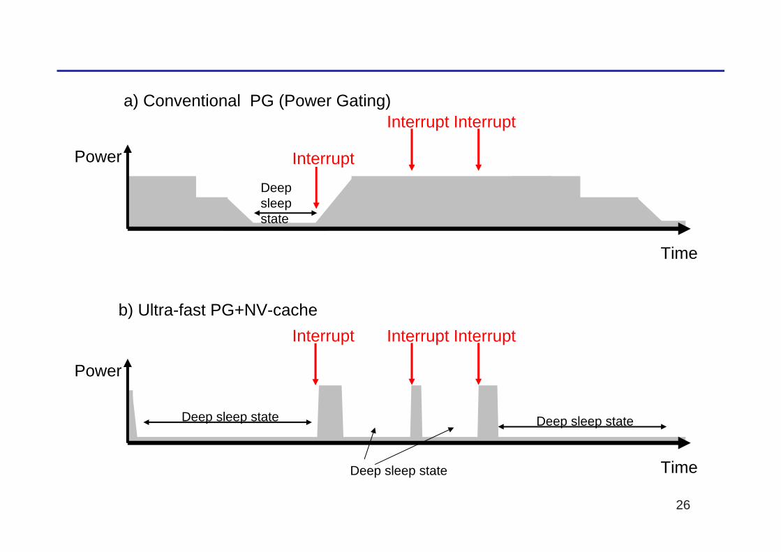
26
a) Conventional PG (Power Gating)
b) Ultra-fast PG+NV-cache
Time
Power Interrupt
Interrupt Interrupt
Time
Power
Interrupt Interrupt Interrupt
Deep sleep state
Deep sleep state
Deep sleep state
Deep sleep state
27
Case 1 Case 2 Case 30
100
200
300
400
500
600
700
800
900
1000
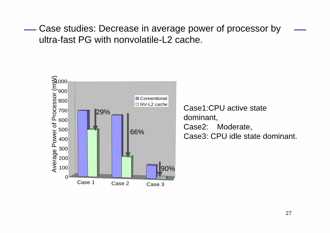
ConventionalNV-L2 cache
29%
66%
90%Ave
rage
Pow
er o
f Pro
cess
or (m
W)
Case studies: Decrease in average power of processor by ultra-fast PG with nonvolatile-L2 cache.
Case1:CPU active state dominant, Case2: Moderate,Case3: CPU idle state dominant.
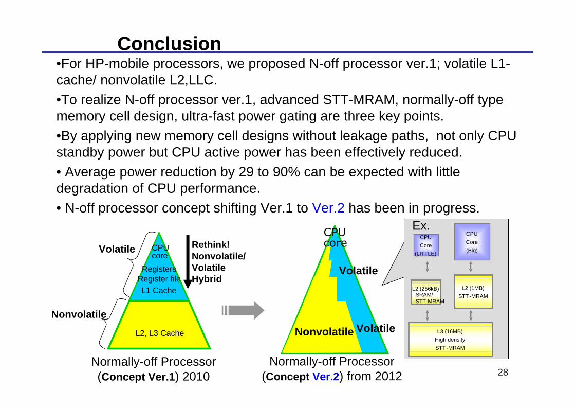
28Normally-off Processor
(Concept Ver.2) from 2012Normally-off Processor(Concept Ver.1) 2010
Volatile Rethink!Nonvolatile/VolatileHybrid
CPU core
Nonvolatile
L2, L3 Cache
L1 CacheRegister fileRegisters
Nonvolatile
Volatile
CPU core
Volatile
Conclusion•For HP-mobile processors, we proposed N-off processor ver.1; volatile L1-cache/ nonvolatile L2,LLC. •To realize N-off processor ver.1, advanced STT-MRAM, normally-off type memory cell design, ultra-fast power gating are three key points.•By applying new memory cell designs without leakage paths, not only CPU standby power but CPU active power has been effectively reduced.• Average power reduction by 29 to 90% can be expected with little degradation of CPU performance.• N-off processor concept shifting Ver.1 to Ver.2 has been in progress.
Ex.
L2 (256kB)SRAM/ STT-MRAM
L3 (16MB)High densitySTT-MRAM
L2 (1MB)STT-MRAM
CPUCore(Big)
CPUCore
(LITTLE)

29
Thank you!