Embed Size (px)
Citation preview
Numerical Simulations of THz
Photoconductive Antenna
by
Aznida Abu Bakar Sajak
thesis submitted in accordance with
the requirement of the University of Liverpool
for the degree of Doctor of Philosophy
Department of Electrical Engineering and Electronics
The University of Liverpool
December 2018
i
Abstract
Terahertz (THz) (0.1 – 10 THz) region of the electromagnetic spectrum spans the
frequency range between the mid-infrared and the millimetre range. THz technology has generated
a lot of interest recently due to its potential applications as a tomographic imaging and material
spectroscopic characterization technique in a wide range of industry sectors including aerospace
industry, wood products industry, the pharmaceutical industry, art conservation and semiconductor
industry. There have been significant advances in the development of THz sources and detectors.
The radiated THz power from these devices, however, is very low, and they are very inefficient.
Hence, there are still a lot of continued interests in developing more powerful and compact THz
sources as this will enable new applications of this electromagnetic spectrum.
In this thesis, a novel photoconductive antenna with an embedded electrode structure had
been proposed. Formulated equations had been used with COMSOL Multiphysics software
package for the proposed THz photoconductive antenna analysis. Simulation results indicate that
the proposed THz antenna can store two times more effective electric energy than the
conventional photoconductive antenna. These results suggest higher THz power could potentially
be obtained using the proposed structure. The proposed model also exhibits almost double the
value of current when the substrate material mobility is doubled.
Based on the appraised parameters of the proposed model, the best dimension of a THz
photoconductive antenna had been recommended to be constructed.
ii
Acknowledgements
First and foremost, I would like to thank my supervisor Professor Yaochun Shen, for his
invaluable guidance and patience in numerous and lengthy discussions throughout the period of my
PhD studies. I am forever grateful for his advice, continuous and generous support and trust in my
capabilities. I would also like to thank Professor Yi Huang who has endorsed this life changing
opportunity for me.
At the Wireless Engineering group, I would also like to express my gratitude to the past
and present members; to Dr. Samuel Lawman for all fruitful discussions, to Dr, Rula Alrawashdeh
and Umniyyah Ulfa Hussine for all good time we had in our office, to Dr. Neda Khiabani for her
inspiring suggestions and time for me. I am delighted that I have found many good friends during
my PhD studies.
Thanks to all my friends, from high-school, college and Malaysian Society who had been
with me in the very crucial moments of my studies and for boosting my morale. I am very grateful
for all their support and effort to cheer me up. In the department, it is a great pleasure to thank the
postgraduate staff, Allison and Hannah for their full support especially in the very challenging
moment of my studies.
I would like to offer my personal and special thanks to my parents and my siblings who
have encouraged me over the years. Primarily this must be my father and mother, who believed in
me and surrounded me with their love and blessing. I must also mention my sister, Azliana for
proof readings my work. I am very thankful for their patience on all my stresses during this journey.
Finally, I should thank the Islamic Development Bank, Saudi Arabia and Universiti Kuala
Lumpur Malaysia for sponsoring my PhD studies. Also the Government of Malaysia for taking
care of me while I am abroad.
iii
List of Publications
1. A. Abu Bakar Sajak, Y. Shen and Y. Huang “Analysis of a Photoconductive Antenna using
COMSOL”, 10th UK-Europe-China Workshop on Milimetre Waves and Terahertz
Technologies (UCMMT), Liverpool, UK, September, 2017.
2. Z. Zhang, L. Liu, A. Abu Bakar Sajak, L. Gan, Y. Huang and Y. Shen, “Spinning disk as
a spatial light modulator for rapid infrared imaging”, IET Microwaves, Antennas &
Propagation, Volume 11, Issue 3, February 2017, p. 317 – 323.
3. R. Alrawashdeh, Y. Huang, M.Kod and A. Abu Bakar Sajak, “A Broadband Flexible
Implantable Loop Antenna With Complementary Split Ring Resonators”, IEEE Antennas
and Wireless Propagation Letters, Volume 14, February 2015, p.1506-1509.
4. A. Abu Bakar Sajak, Y. Shen, Y. Huang, and R. Alrawashdeh, “A Comparison of the
Effect of Substrate on the Performance of THz Antenna”, Proceeding of the ICE2T,
Malaysia, August, 2014.
5. Q. Xu, Y. Huang, X. Lei and A. Abu Bakar Sajak, “Statistical Electromagnetic Analysis
of PEC Sphere Scattering”, Proceeding of the ICE2T, Malaysia, August, 2014.
6. R. Alrawashdeh, Y. Huang, and A. Abu Bakar Sajak, “Orientation Effect of Flexible
Implantable Antennas on Performance,” 2014 IEEE International Symposium on Antennas
and Propagation and USNC-URSI National Radio Science Meeting , Memphis, Tennessee,
USA, July, 2014.
7. A. Abu Bakar Sajak, Y. Shen, Y. Huang, and R. Alrawashdeh, “The Effect of Substrate
on the Performance of THz Antenna”, IET Colloquium on Millimetre-wave and Terahertz
Engineering & Technology, Liverpool, UK, 2014.
iv
8. A. Abu Bakar Sajak, Y. Shen, Y. Huang, and R. Alrawashdeh, “An Investigation on THz
Antennas Using Graphene as a Substrate”, The 8th European Conference on Antennas and
Propagation, The Hague, The Netherlands, April, 2014.
9. R. Alrawashdeh, Y. Huang, and A. Abu Bakar Sajak, “A Flexible Loop Antenna for
Biomedical Bone Implants”, The 8th European Conference on Antennas and Propagation,
The Hague, The Netherlands, April 2014.
10. N. Khiabani, Y. Huang, Y. Shen, and A. Abu Bakar Sajak, “Photoconductive THz
Antennas Loughborough Antennas & Propagation Conference, Loughborough, UK,
November 2013.
v
Table of Contents Page
ABSTRACT i
ACKNOWLEDGEMENTS ii
LIST OF PUBLICATIONS iii
TABLE OF CONTENT v
LIST OF TABLES x
LIST OF FIGURES xi
LIST OF ABBREVIATIONS xviii
CHAPTER
1 Introduction
1.1 The Terahertz Spectrum 1
1.2 The THz Wave Properties and Applications 2
1.2.1 Atmospheric Characteristics of THz Waves 3
1.2.2 Applications of THz Radiation 4
1.2.2.1 THz Pulsed System Applications 4
1.2.2.2 THz CW applications 7
1.3 THz Sources 7
1.3.1 THz Sources from RF/MW Side 8
1.3.1.1 Diodes and Frequency Multipliers 8
1.3.1.2 THz Vacuum Tube Sources 8
1.3.2 THz Sources from Optical Side 9
1.3.2.1 Molecular Lasers 9
1.3.2.2 THz Semiconductor Lasers 9
1.3.2.3 Optical Down Converters 10
1.3.3 THz Sources Combining RF/MW and Optical Techniques 11
1.4 THz Detectors 12
1.5 Research Motivations and Objectives 14
1.6 Thesis Overview 16
References 18
vi
2 THz Photoconductive Antennas
2.1 Introduction 25
2.2 The Importance of Having a THz Antenna in a THz System 25
2.3 The THz Photoconductive Antenna 26
2.3.1 Theoretical Principle of THz Photoconductive Antenna as an
Emitter
27
2.3.1.1 Large-Aperture Antennas 27
2.3.1.2 Small Gap Antennas 28
2.3.2 Theoretical Principle of a THz Photoconductive Antenna as
a Detector
30
2.4 Comparison of THz Antennas with RF/MW Antennas 31
2.4.1 Fabrication and Measurement 32
2.4.2 Feeding, Excitation Source and Biasing 33
2.4.3 Electrode Material 34
2.4.4 Substrate Material 35
2.4.5 Type of Current 39
2.4.6 Computer Aided Design 39
2.5 Problems of THz Photoconductive Antennas 40
2.5.1 Problems Related to THz Photoconductive Antennas 41
2.6 Previous work on THz Photoconductive
Antennas
42
2.6.1 Varying Antenna Gap Area Geometry 43
2.6.2 Improving Optical Power Coupling 43
2.7 Summary 48
References 49
3 A Comparison of the Effect of Substrate on the Performance of THz Antenna
3.1 Introduction 60
3.2 Previous Investigation on the Effects of Substrate
on THz Antennas
62
3.3 Simulation Results 65
3.3.1 Substrate Thickness 65
3.3.2 Substrate Material 68
vii
3.4 Summary 71
References 73
4 The Effect of Electrode Design on THz Photoconductive Antenna 75
4.1 Introduction 75
4.2 The Importance of the Electrode Study 77
4.2.1 Electrode Structure Study 77
4.2.2 Electrode Material Study 78
4.3 Electrode structure study using CST 79
4.3.1 Methodology 79
4.3.2 The Simulation Results 81
4.4 Electrode material study using CST 84
4.4.1 The Advantages of Plasmonic Metamaterial 84
4.4.1.1 Surface Plasmon Excitation 84
4.4.1.2 High Loss of Noble Metals 87
4.4.2 Methodology 88
4.4.3 The Simulation Results 88
4.5 Summary 91
References 92
5 Analysis of a Photoconductive Antenna using COMSOL 95
5.1 Introduction 95
5.2 Simulation Method 97
5.3 Simulation Results 97
5.3.1 Electrode Thickness 97
5.3.2 Substrate Mobility 101
5.3.3 Antenna Gap 104
5.3.4 Substrate Thickness 105
5.3.5 Material comparison 105
5.4 Summary 108
References 110

viii
6 Conclusions and Future Work 111
6.1 Conclusions 111
6.2 Future Work 114
Appendix A E-field of THz Small and Large Gap Antennas 116
Appendix B Calculation of Efficiencies 120
ix
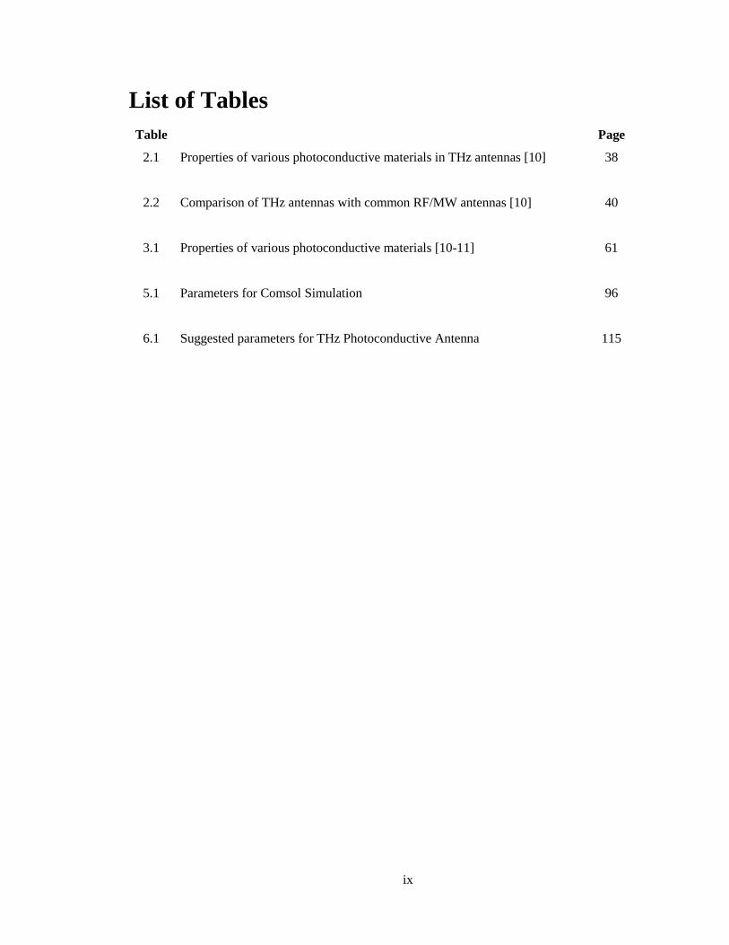
List of Tables
Table Page
2.1 Properties of various photoconductive materials in THz antennas [10] 38
2.2 Comparison of THz antennas with common RF/MW antennas [10] 40
3.1 Properties of various photoconductive materials [10-11] 61
5.1 Parameters for Comsol Simulation 96
6.1 Suggested parameters for THz Photoconductive Antenna 115
x
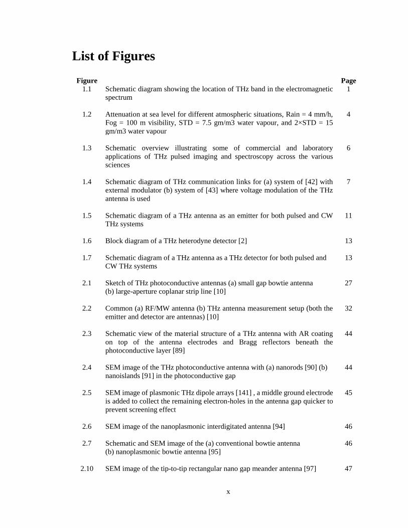
List of Figures
Figure Page
1.1 Schematic diagram showing the location of THz band in the electromagnetic
spectrum
1
1.2 Attenuation at sea level for different atmospheric situations, Rain = 4 mm/h,
Fog = 100 m visibility, STD = 7.5 gm/m3 water vapour, and 2×STD = 15
gm/m3 water vapour
4
1.3 Schematic overview illustrating some of commercial and laboratory
applications of THz pulsed imaging and spectroscopy across the various
sciences
6
1.4 Schematic diagram of THz communication links for (a) system of [42] with
external modulator (b) system of [43] where voltage modulation of the THz
antenna is used
7
1.5 Schematic diagram of a THz antenna as an emitter for both pulsed and CW
THz systems
11
1.6 Block diagram of a THz heterodyne detector [2] 13
1.7 Schematic diagram of a THz antenna as a THz detector for both pulsed and
CW THz systems
13
2.1 Sketch of THz photoconductive antennas (a) small gap bowtie antenna
(b) large-aperture coplanar strip line [10]
27
2.2 Common (a) RF/MW antenna (b) THz antenna measurement setup (both the
emitter and detector are antennas) [10]
32
2.3 Schematic view of the material structure of a THz antenna with AR coating
on top of the antenna electrodes and Bragg reflectors beneath the
photoconductive layer [89]
44
2.4 SEM image of the THz photoconductive antenna with (a) nanorods [90] (b)
nanoislands [91] in the photoconductive gap
44
2.5 SEM image of plasmonic THz dipole arrays [141] , a middle ground electrode
is added to collect the remaining electron-holes in the antenna gap quicker to
prevent screening effect
45
2.6 SEM image of the nanoplasmonic interdigitated antenna [94] 46
2.7 Schematic and SEM image of the (a) conventional bowtie antenna
(b) nanoplasmonic bowtie antenna [95]
46
2.10 SEM image of the tip-to-tip rectangular nano gap meander antenna [97] 47

xi
2.11 Microscopic images of the THz bowtie antenna with trapezoidal tip-to-tip
fingers (a) overall antenna view (b) zoom-in of the photomixer section (c)
SEM zoom-in of the trapezoidal tip-to-tip finger (d) SEM zoom-in of a
nanogap trapezoidal finger [98]
47
3.1 2D of Graphene [2] 61
3.2 Schematic diagram of a THz antenna as an emitter [16-17] 62
3.3 Dipole antenna [8] surrounded by air and its radiation pattern 63
3.4 Dipole antenna [8] on a GaAs substrate and its radiation pattern 64
3.5 Total radiated power when substrate thickness is varied while length and the
width of the substrate are both fixed to 150 µm
66
3.6 Total efficiency when substrate thickness is varied while length and the
width of the substrate are both fixed to 150 µm
66
3.7 Total radiated power when substrate thickness fixed to 75µm while the
length and width are varies
67
3.8 Total efficiency when substrate thickness fixed to 75µm while the length and
width are varies
68
3.9 Total radiated power for various photoconductive materials 69
3.10 A radiation pattern of a dipole antenna in [1] with GaAs as a substrate 70
3.11 A radiation pattern of a dipole antenna in [1] with Graphene as a substrate 70
3.12 Total efficiency for various photoconductive material 71
4.1 Contribution of each parameter on THz output power and optical-to THz
conversion efficiency [1-3]
76
4.2 Framework on the contributions to produce high photo-carriers 77
4.3 Framework on the contributions to produce high optical power coupling 78
4.4 Summary of Contribution to High Optical Power Coupling 78
4.5 The dipole antenna used in electrode structure study using CST 80
4.6 The structure of dipole antenna and their wireframe with (a) standard electrode
(b) embedded electrode
80
4.7 The radiated power of dipole antenna using standard electrode and an
embedded electrode, 2 µm into the substrate
82
xii
4.8 The efficiency of the dipole antenna using standard electrode and an embedded
electrode, 2 µm into the substrate
83
4.9 Comparison done on the dielectric function of plasmonic metamaterial TiN
with conventional metals [14-15]
88
4.10 The radiated power of dipole antenna using an electrode made from noble
metals and metamaterial
90
4.11 The 3D pattern of the farfield of dipole antenna using graphene as an electrode
is shown in dBi
90
4.12 The 3D pattern of the farfield of dipole antenna using gold as an electrode is
shown in dBi
91
4.13 The 3D pattern of the farfield of dipole antenna using silver as an electrode is
shown in dBi
91
4.14 The 3D pattern of the farfield of dipole antenna using TiN as an electrode is
shown in dBi
92
5.1 The structure of a (a) conventional model photoconductive antenna and (b)
proposed model photoconductive antenna
96
5.2 Schematic diagram of the structure of a photoconductive antenna (a)
conventional model (b) proposed model and the coordinate of the simulated
electric field
96
5.3 Electric Field of (a) conventional (b) proposed THz photoconductive antenna
at given voltage bias at 4 V
97
5.4 Electric Field of the proposed photoconductor and the conventional
photoconductor at 4V voltage bias
98
5.5 Electric Field of the proposed photoconductor of 1 μm electrode thickness and
the conventional photoconductor at 4V voltage bias
99
5.6 Electric field of proposed THz photoconductive antenna with 0.1 um electrode
thickness from (a) electric current module (b) electromagnetic module
simulated in COMSOL Multiphysics
100
5.7 Total effective energy of the conventional photoconductor vs proposed
photoconductor at 4V voltage bias and various laser power
101
5.8 Current density of the proposed model at different depth using GaAs as the
substrate using its actual carrier mobility of 8500 cm2/Vs – straight line and
half of the carrier mobility of 4500 cm2/Vs - dashed line
102
5.9 Total current density plot of the proposed model at 1 µm depth using GaAs as
the substrate using (a) half of its carrier mobility of 4500 cm2/Vs and (b) actual
carrier mobility of 8500 cm2/Vs at 4V
103
xiii
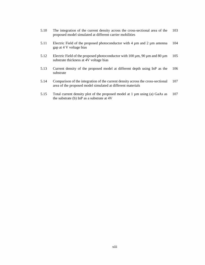
5.10 The integration of the current density across the cross-sectional area of the
proposed model simulated at different carrier mobilities
103
5.11 Electric Field of the proposed photoconductor with 4 µm and 2 µm antenna
gap at 4 V voltage bias
104
5.12 Electric Field of the proposed photoconductor with 100 µm, 90 µm and 80 µm
substrate thickness at 4V voltage bias
105
5.13 Current density of the proposed model at different depth using InP as the
substrate
106
5.14 Comparison of the integration of the current density across the cross-sectional
area of the proposed model simulated at different materials
107
5.15 Total current density plot of the proposed model at 1 µm using (a) GaAs as
the substrate (b) InP as a substrate at 4V
107

xiv
List of abbreviation
AlGaAs Aluminium Gallium Arsenide
AR Anti-Reflection
BW Bandwidth
BWO Backward Wave Oscillator
CAD Computer Aided Design
CW Continuous Wave
CPW Coplanar Waveguide
DFG Difference Frequency Generation
EM ElectroMagnetic
EO Electro-Optic
ErAs Erbium Arsenide
FDTD Finite Difference Time Domain
FWHM Full Width at Half Maximum
GaAs Gallium Arsenide
HEB Hot Electron Bolometer
IMPATT IMPact Avalanche and Transit Time
ITO Indium Tin Oxides
LEC Liquid Encapsulated Czochralski
LT-GaAs Low Temperature-GaAs
MBE Molecular Beam Epitaxy
MEMS MicroElectroMechanical System
MMIC Monolithic Microwave Integrated Circuits
MW Microwave
xv
QCL Quantum-Cascade lasers
QTDS Quasi Time Domain Spectroscopy
RF Radio Frequency
RTD Resonant Tunnelling Diodes
RX Receiver
SEM Scanning Electron Microscopy
Si Silicon
SI-GaAs Semi-Insulating GaAs
SI-InP Semi-Insulating Indium phosphide
SIS Superconductor–Insulator– Superconductor
SNR Signal-to-Noise Ratio
TEM Transverse ElectroMagnetic
THz Terahertz
THz-TDI THz Time Domain Imaging
THz-TDS THz Time Domain Spectroscopy
Ti Titanium
TWT Travelling Wave Tube
TX Transmitter
ZnTe Zinc Telluride
1
Chapter 1 Introduction
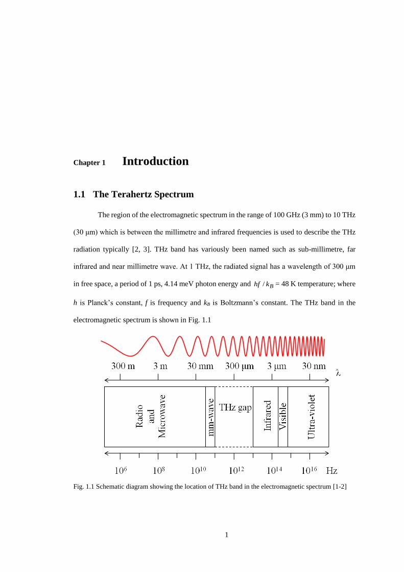
1.1 The Terahertz Spectrum
The region of the electromagnetic spectrum in the range of 100 GHz (3 mm) to 10 THz
(30 μm) which is between the millimetre and infrared frequencies is used to describe the THz
radiation typically [2, 3]. THz band has variously been named such as sub-millimetre, far
infrared and near millimetre wave. At 1 THz, the radiated signal has a wavelength of 300 μm
in free space, a period of 1 ps, 4.14 meV photon energy and = 48 K temperature; where
h is Planck’s constant, f is frequency and kB is Boltzmann’s constant. The THz band in the
electromagnetic spectrum is shown in Fig. 1.1
Fig. 1.1 Schematic diagram showing the location of THz band in the electromagnetic spectrum [1-2]
Bkhf /
2
Due to the absence of efficient, coherent, and compact THz sources and detectors, this
segment of the electromagnetic spectrum is the least explored region [3, 4]. Common
microwave-frequency sources such as transistors or RF/MW antennas and devices working in
the visible and infrared range, for example, semiconductor laser diodes exhibit these
characteristics [5]. Due to the significant reduction in power and efficiency, it is not possible to
adopt these technologies for operation in the THz region. Solid-state electronic devices, such
as diodes generated power that has roll-offs of 1/ f 2 [6] due to reactive-resistive effects and
long transit times at the lower extreme of THz frequency range [6]. Furthermore, lack of
materials with adequately small bandgap energies [5] making optical devices, such as diode
lasers, perform poorly at THz range limit. Therefore, the term “THz gap” is invented to explain
the lack of maturity of this band compared to fully developed adjacent spectral regions. Various
types of research on new emitters and detectors based on semiconductor technology are
emerging to address these issues [4, 7-9].
In this chapter, the THz radiation is explained. Its properties and application are
discussed. Then, different THz sources and detectors are reviewed and evaluated. Based on the
built foundation, the research motivations and objectives of this thesis are outlined.
1.2 The THz Wave Properties and Applications
Interest in THz region dates back to 1920s [30], though only within the past three
decades extensive research has been dedicated to this spectrum. Endless applications possibility
in the THz frequency range and remarkable wave properties is the reason for the sudden interest
in the region. Since THz region is contained between microwave-millimetre and infrared areas
it has mid-characteristics borrowed from the two bands. These properties can be summarised
as follows [1-2]:
1. Penetration: The wavelength of THz radiation is longer than the infrared
wavelength; hence, THz waves have less scattering and better penetration depths
(~ cm) compared to infrared ones (~ μm). Therefore, dry and non-metallic
materials are transparent in this range but are opaque in the visible spectrum.
3
2. Safety: In contrary to X-rays, the photon energies in the THz band are much lower.
Therefore, THz radiation is non-ionising.
3. Spectral fingerprint: Inter- and intra-vibrational modes of many molecules lie in
THz range.
4. Resolution: THz waves have shorter wavelengths in comparison to the microwave
ones, this gives a better spatial imaging resolution.
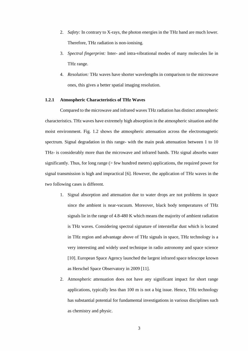
1.2.1 Atmospheric Characteristics of THz Waves
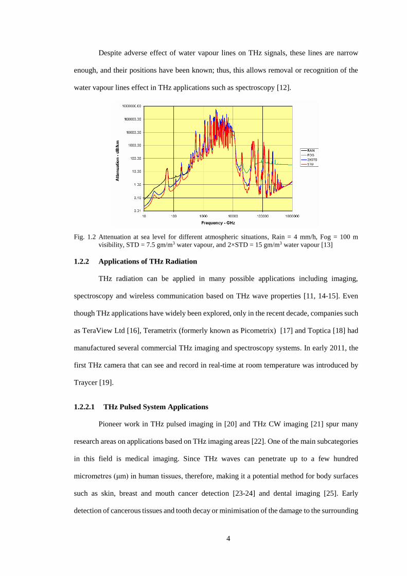
Compared to the microwave and infrared waves THz radiation has distinct atmospheric
characteristics. THz waves have extremely high absorption in the atmospheric situation and the
moist environment. Fig. 1.2 shows the atmospheric attenuation across the electromagnetic
spectrum. Signal degradation in this range- with the main peak attenuation between 1 to 10
THz- is considerably more than the microwave and infrared bands. THz signal absorbs water
significantly. Thus, for long range (> few hundred meters) applications, the required power for
signal transmission is high and impractical [6]. However, the application of THz waves in the
two following cases is different.
1. Signal absorption and attenuation due to water drops are not problems in space
since the ambient is near-vacuum. Moreover, black body temperatures of THz
signals lie in the range of 4.8-480 K which means the majority of ambient radiation
is THz waves. Considering spectral signature of interstellar dust which is located
in THz region and advantage above of THz signals in space, THz technology is a
very interesting and widely used technique in radio astronomy and space science
[10]. European Space Agency launched the largest infrared space telescope known
as Herschel Space Observatory in 2009 [11].
2. Atmospheric attenuation does not have any significant impact for short range
applications, typically less than 100 m is not a big issue. Hence, THz technology
has substantial potential for fundamental investigations in various disciplines such
as chemistry and physic.
4
Despite adverse effect of water vapour lines on THz signals, these lines are narrow
enough, and their positions have been known; thus, this allows removal or recognition of the
water vapour lines effect in THz applications such as spectroscopy [12].
Fig. 1.2 Attenuation at sea level for different atmospheric situations, Rain = 4 mm/h, Fog = 100 m
visibility, STD = 7.5 gm/m3 water vapour, and 2×STD = 15 gm/m3 water vapour [13]
1.2.2 Applications of THz Radiation
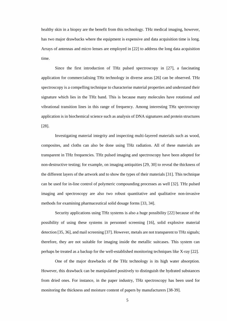
THz radiation can be applied in many possible applications including imaging,
spectroscopy and wireless communication based on THz wave properties [11, 14-15]. Even
though THz applications have widely been explored, only in the recent decade, companies such
as TeraView Ltd [16], Terametrix (formerly known as Picometrix) [17] and Toptica [18] had
manufactured several commercial THz imaging and spectroscopy systems. In early 2011, the
first THz camera that can see and record in real-time at room temperature was introduced by
Traycer [19].
1.2.2.1 THz Pulsed System Applications
Pioneer work in THz pulsed imaging in [20] and THz CW imaging [21] spur many
research areas on applications based on THz imaging areas [22]. One of the main subcategories
in this field is medical imaging. Since THz waves can penetrate up to a few hundred
micrometres (μm) in human tissues, therefore, making it a potential method for body surfaces
such as skin, breast and mouth cancer detection [23-24] and dental imaging [25]. Early
detection of cancerous tissues and tooth decay or minimisation of the damage to the surrounding
5
healthy skin in a biopsy are the benefit from this technology. THz medical imaging, however,
has two major drawbacks where the equipment is expensive and data acquisition time is long.
Arrays of antennas and micro lenses are employed in [22] to address the long data acquisition
time.
Since the first introduction of THz pulsed spectroscopy in [27], a fascinating
application for commercialising THz technology in diverse areas [26] can be observed. THz
spectroscopy is a compelling technique to characterise material properties and understand their
signature which lies in the THz band. This is because many molecules have rotational and
vibrational transition lines in this range of frequency. Among interesting THz spectroscopy
application is in biochemical science such as analysis of DNA signatures and protein structures
[28].
Investigating material integrity and inspecting multi-layered materials such as wood,
composites, and cloths can also be done using THz radiation. All of these materials are
transparent in THz frequencies. THz pulsed imaging and spectroscopy have been adopted for
non-destructive testing; for example, on imaging antiquities [29, 30] to reveal the thickness of
the different layers of the artwork and to show the types of their materials [31]. This technique
can be used for in-line control of polymeric compounding processes as well [32]. THz pulsed
imaging and spectroscopy are also two robust quantitative and qualitative non-invasive
methods for examining pharmaceutical solid dosage forms [33, 34].
Security applications using THz systems is also a huge possibility [22] because of the
possibility of using these systems in personnel screening [16], solid explosive material
detection [35, 36], and mail screening [37]. However, metals are not transparent to THz signals;
therefore, they are not suitable for imaging inside the metallic suitcases. This system can
perhaps be treated as a backup for the well-established monitoring techniques like X-ray [22].
One of the major drawbacks of the THz technology is its high water absorption.
However, this drawback can be manipulated positively to distinguish the hydrated substances
from dried ones. For instance, in the paper industry, THz spectroscopy has been used for
monitoring the thickness and moisture content of papers by manufacturers [38-39].
6
Finally, a very convenient method to take 3D images from the inside of an integrated
circuit device can be done using THz pulsed imaging. This is better compared to the 2D images
provided by the X-ray method [22].
In a nutshell, a schematic overview of various THz applications based upon
optoelectronic systems is depicted in Fig. 1.3 [1,2].
Fig. 1.3 Schematic overview illustrating some commercial and laboratory applications of THz pulsed
imaging and spectroscopy across the various sciences [1]
THz application in wireless communication, one interesting THz application which
cannot be categorised in either THz pulsed imaging or spectroscopy. To provide sufficient
transmission capacity for future high data rate demands, higher carrier frequencies need to be
utilized, and THz frequencies had the potential to satisfy these needs. However, THz
communication links have two main limitations where THz communication systems are only
suitable for line of sight cases, and THz signals can only propagate over a short path length
due to severe atmospheric attenuation. Considering these restrictions, THz communication
systems can be a suitable option for indoor short distances which is limited to several tens of
meters such as multipoint to point/multipoint basis at frequencies between about 0.2 to 0.3 THz
[40]. From another point of view, these restrictions are beneficial for secure THz
communication since the beam can be highly directional and it attenuates severely over the
distance; unwanted signal detection is difficult. THz data communications for short ranges less
than < 1m is based upon THz time domain systems and have been tested at 0.3 THz in recent
years [41]. In [42] external semiconductor THz modulator is used with data transmission of 6
kHz while in [43] audio signals through the voltage of the transmitter THz antenna modulates
7
the THz frequency, and the reported data transmission was 5 kb/s. Block diagrams of these two
approaches are demonstrated in Fig. 1.4.
(a)
(b)
Fig. 1.4 Schematic diagram of THz communication links for (a) system of [42] with external modulator
(b) system of [43] where voltage modulation of the THz antenna is used
1.2.2.2 THz CW applications
Narrowband high resolution systems are required for some applications such as gas-
phase spectroscopy, high frequency dielectric measurements of electronic, metamaterials and
nano-materials, and signature analysing in microliter DNA [22,44-46]. This opportunity can be
realised via THz CW imaging and spectroscopy systems [47-48]. For some applications like
imaging of aircraft glass-fibre composites or determining the thickness of a sample however
both pulsed and CW imaging methods can be used [41, 49].
1.3 THz Sources
Among all the elements in THz technology, the THz source has been considered as the
most challenging component to accomplish [26]. Numerous research and effort have been done
to extend RF/MW and optical technologies to THz band. Combining both of the technologies
8
to realise THz sources with better performance had also been considered [50]. Due to this effort,
THz emitters are divided into three main groups: THz sources developed from RF/MW side,
THz sources extended from optical side, and THz sources combining RF/MW and optical
techniques.
1.3.1 THz Sources from RF/MW Side
In this category, diodes and THz vacuum tube sources are explained.
1.3.1.1 Diodes and Frequency Multipliers
On the lower end of the THz spectrum, diodes can transfer the functionality of lower
frequency electronics into the THz band. There are several types of diodes, such as Gunn
diodes, IMPATT diodes and resonant tunnelling diodes (RTD). The principle of power
generation from these diodes is based upon their negative differential resistance [51] although
the operation bases of these diodes are different. Each of these diodes has their own advantages
and disadvantages [51-56]. Still, in these components, dramatic reduction in powers can be
observed with increasing frequency [53].
Another method to reach THz band is the use of frequency multipliers which
outperform other solid-state electronic sources. This is because the diode multipliers are
physically and operationally simple [52]. Since higher order multipliers are incredibly
inefficient, series arrangements of doublers and triplers have mostly been implemented [26]. In
this method, chains of microwave sources, such as GaAs Schottky diodes, at lower GHz bands
(20 – 40 GHz) can be used in series to drive multiplication at THz ranges [52]. However, the
output power from multipliers decreases at higher frequencies [57], like the diodes mentioned
above. The bandwidth of these sources is also limited [57].
1.3.1.2 THz Vacuum Tube Sources
Free electrons emission from microwave tubes is one of the traditional THz generation
methods. THz tubes such as travelling wave tube (TWT), backward wave oscillator (BWO),
klystron and gyratron can produce strong power levels at the lower end of THz band. In [58] a
9
power level of 52 mW at about 0.6 THz from a BWO has been reported. One of the main
operational similarities in all of these tubes is the interaction of an electron beam with an
electromagnetic wave to produce THz energy. Although THz tubes can produce much stronger
power levels at the lower end of THz band compared to previously explained solid-state
components [51], they are very bulky. They also need large magnetic biases and high voltage
power supplies. This restricts the use of these sources in wide operational settings, making it
inflexible.
1.3.2 THz Sources from Optical Side
THz sources from optical side are mainly divided into lasers with different generation
techniques and nonlinear crystals [2].
1.3.2.1 Molecular Lasers
THz signals with a power level of few ten milliwatts can be produced by injecting
grating tuned CO2 lasers into low-pressure flowing gas cavities [2,26]. The frequency of this
THz power depends on the spectral line of the gas; for example, a rotational transition of
methanol occurs at 2.522 THz.
1.3.2.2 THz Semiconductor Lasers
Semiconductor diode lasers are very successful and prevalent in the near-infrared and
visible frequency ranges. In THz bands, natural materials with suitable band gaps are not
available, artificially engineered materials are considered [5, 59]. Therefore, the concept of THz
Quantum-Cascade lasers (QCL) which are intra-band lasers and require the creation of
quantised sub-bands was introduced [4]. For this purpose, several few-nm-thick GaAs layers
separated by AlGaAs barriers need to be fabricated. Therefore, proper engineering of the
thickness of the semiconductor layers (or quantum wells) and also a choice of the appropriate
bias voltage is required to achieve population inversion. Because the energy of the system is
inversely proportional to the square of the layers thicknesses, by narrowing or widening the
10
quantum wells, series of multi layers of energy can be created. Thus, the electron motion from
one miniband to the next results in an emission of a THz photon at each transition.
QCL can operate in both pulsed and continuous-wave (CW) modes. QCL operating
frequency is controlled by quantum well design (band gap engineering), and different
wavelengths can be achieved in the same material [2]. QCLs have been one of the most
intensive research topics in THz area during the past decade and the survey on different THz
QCLs show that the frequency ranges of these devices span from 0.84 THz to 5 THz at various
cryogenic working temperatures [60-63] with the best peak optical power of 200 mW at about
4.5 THz [5] . The best peak operating temperature of 200 K at about 3.2 THz reported in [64].
In room temperature situation, a THz QCL with a power of 8.5 μW at 4 THz has been
demonstrated [65].
As a conclusion, QCLs have larger output power at higher THz frequencies and as
frequency decreases the power reduces considerably [2]. One of the main limitations of THz
QCLs is that for THz operation they need cryogenic cooling and this restricts the operation of
QCLs to only laboratory environments making it unattractive.
1.3.2.3 Optical Down Converters
One of the common methods for THz generation is the use of nonlinear crystals with
large second order susceptibility, χ, for down conversion of power from optical regime [2].
Several nonlinear materials for this purpose can be employed [11]. THz parametric processes
such as parametric oscillator or difference frequency generation (DFG) are techniques for
production of monochromatic highly tunable THz wave sources with a high spectral resolution
[66-68]. Another optical down conversion method is the optical rectification in which all
possible difference frequencies of spectrally broad optical pulses are generated.
The drawbacks of this method are that the phase matching between the optical fields
and induced THz field is needed. This requires thorough design on the thickness of the
nonlinear material. The THz output power in this method is low, and to generate significant
THz power, high power optical sources are needed.
11
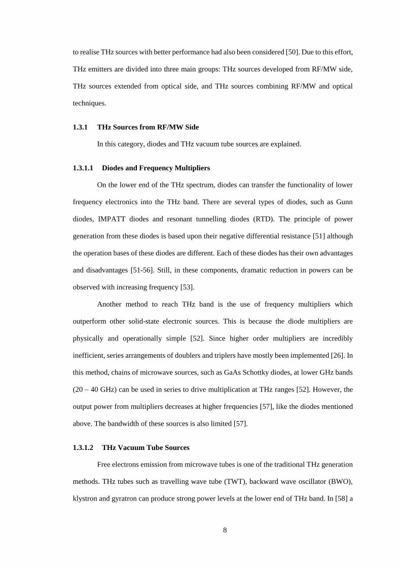
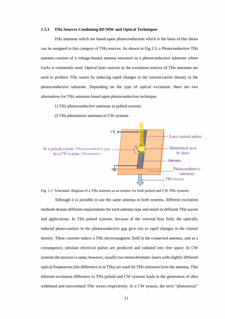
1.3.3 THz Sources Combining RF/MW and Optical Techniques
THz antennas which are based upon photoconduction which is the basis of this thesis
can be assigned to this category of THz sources. As shown in Fig.1.5, a Photoconductive THz
antenna consists of a voltage-biased antenna mounted on a photoconductive substrate where
GaAs is commonly used. Optical laser sources as the excitation sources of THz antennas are
used to produce THz waves by inducing rapid changes in the current/carrier density in the
photoconductive substrate. Depending on the type of optical excitation, there are two
alternatives for THz antennas based upon photoconduction technique:
1) THz photoconductive antennas in pulsed systems
2) THz photomixer antennas in CW systems
Fig. 1.5 Schematic diagram of a THz antenna as an emitter for both pulsed and CW THz systems
Although it is possible to use the same antenna in both systems, different excitation
methods dictate different requirements for each antenna type and result in different THz waves
and applications. In THz pulsed systems, because of the external bias field, the optically
induced photo-carriers in the photoconductive gap give rise to rapid changes in the current
density. These currents induce a THz electromagnetic field in the connected antenna, and as a
consequence, ultrafast electrical pulses are produced and radiated into free space. In CW
systems the process is same; however, usually two monochromatic lasers with slightly different
optical frequencies (the difference is in THz) are used for THz emission from the antenna. This
inherent excitation difference in THz pulsed and CW systems leads to the generation of ultra
wideband and narrowband THz waves respectively. In a CW system, the term “photomixer”
12
refers to the antenna gap (which can have various designs) in an analogy of “photoconductive
gap” in a THz pulsed system. The focus of this thesis will be on these types of sources. Detailed
and comprehensive study and investigation on THz antennas will be presented in next chapters.
1.4 THz Detectors
Compared to emitters/sources, development in THz detectors has been more
aggressive [26]. One of the main issues in the detection of THz waves is that the photon energy
in this frequency band is in the range of 0.41 to 41 meV which is comparable to the background
thermal noise energy. Therefore, to overcome this problem mainly two methods have been
adopted: cryogenic cooling and signal integration for long enough periods [26].
THz detection can be categories into coherent and incoherent techniques. The main
difference between them is that in coherent technique both the amplitude and phase of the
received signal are determined. Meanwhile, an incoherent technique only the intensity of the
signal is measured [2].
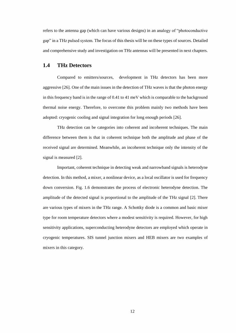
Important, coherent technique in detecting weak and narrowband signals is heterodyne
detection. In this method, a mixer, a nonlinear device, as a local oscillator is used for frequency
down conversion. Fig. 1.6 demonstrates the process of electronic heterodyne detection. The
amplitude of the detected signal is proportional to the amplitude of the THz signal [2]. There
are various types of mixers in the THz range. A Schottky diode is a common and basic mixer
type for room temperature detectors where a modest sensitivity is required. However, for high
sensitivity applications, superconducting heterodyne detectors are employed which operate in
cryogenic temperatures. SIS tunnel junction mixers and HEB mixers are two examples of
mixers in this category.

13
Fig. 1.6 Block diagram of a THz heterodyne detector [2]
Electro-Optic (EO) and photoconduction samplings are also coherent methods. In the
former, the amplitude and phase of the THz signal are measured by using a nonlinear crystal.
In the photoconduction samplings as shown in Fig. 1.7, the THz signal induces a voltage across
the antenna which leads to a generation of THz current due to the existence of free electron-
hole pairs in the antenna gap. The phase of the THz signal in these methods can be measured
by varying the optical path length of the optical probe pulse.
Other incoherent detectors are direct detectors such as Golay cells and bolometers.
These detectors in room temperature are appropriate for applications where high spectral
resolution and rapid response time in the order of seconds are not required [26]. For a better
sensitivity and dynamic range, cryogenic cooled direct detectors such as cryogenically cooled
bolometers which have a response time in the order of microseconds can be used [26].
Fig. 1.7 Schematic diagram of a THz antenna as a THz detector for both pulsed and CW THz systems
[2]
14
1.5 Research Motivations and Objectives
The primary motivation for this research is triggered by the limitation in the
development of high output power and efficient sources in the fast growing THz technology.
Though light and radio waves belong to the same electromagnetic spectrum, their
behaviour is different. THz region is the intermediate part of the spectrum which has a mixture
of both characteristics. Despite the fascinating and unique properties, THz technology has been
largely avoided by the late of the twentieth century due to the lack of robust, coherent, efficient
and cost effective THz sources and detectors [1-2]. However, the advent of femtosecond lasers
in the 1980s and later photoconductive antennas in 1984 [68], developed accessibility to THz
gap. Since then and over the last three decades, due to interests in new THz applications in
different fields as discussed previously, THz technology has undergone extraordinary progress.
Commercial THz imaging and spectroscopy systems have started to be introduced to the
market. Still, there are various issues, such as the low output power and working temperature
of THz sources, which need to be tackled for this technology to be as mature as radio and optical
technologies.
THz photoconductive antennas are one of the keys and common components in many
THz systems. The popularity of these THz antennas is because of the several advantages that
these types of THz sources are offered as compared to other THz sources discussed earlier. For
instance, they work in a room-temperature environment, they are compact, and they can operate
both in the emitter and detector sides [1-2].
Although these types of components have been widely employed in established THz
systems, the radiated power from them is very low, which is about few microwatts, and they
are inefficient [69]. For this purpose, it is crucial to establish the effect of various parameters
of optical sources, photoconductive materials and antennas on the performance of the THz
antennas. Thus, having a model which links these parameters can be very useful for both,
designing a THz antenna and tuning a THz system to achieve the optimum power conversion
efficiency and THz radiated power. Therefore, as fundamental research work on the THz
15
photoconductive antennas, a numerical model is developed in this study considering the
interaction between laser beams, photoconductive materials and antennas in a typical THz
scheme.
Utilising a package of commercial simulation tool is an essential part of radio
frequency (RF) antenna analysis. This step is crucial to determine the necessary parameters
before preceding to any experimental procedure. However, the major difference in analysing
THz antennas as compared to RF antennas is the optoelectronic characteristics of THz antennas
which are the result of the optical excitation and photoconductive material response. Some
commercial semiconductor solvers such as TCAD Sentaurus [70] and COMSOL [71] perform
advanced simulations on characterising semiconductor devices considering their complex
physical phenomena, and various information for instance on electric field distribution and
charge concentration can be provided by them. Sentaurus is a suite of TCAD tools which
simulates the fabrication, operation and reliability of semiconductor devices, but COMSOL
COMSOL Multiphysics is a cross-platform finite element analysis, solver and multiphysics
simulation software. One software product with a lot of different modules. COMSOL offers a
single and comprehensive software set. One advantage provided through COMSOL is the ease
of setting up a multi-physics simulation. With one pre-processor, solver and post-processor,
simulation analysts don’t have to use a wide range of tools to get one job done. COMSOL is a
consolidated environment hence simulation analysts don’t have to worry about mapping the
results of one simulation onto another simulation. For THz antenna analysis, the THz current
source is the main input that needs to be fed to full-wavelength simulation tools. This
combination of semiconductor solvers with full-wave electromagnetic solvers can provide a
possibility of simulation of THz antennas, and this method can predict the outcome of any
experimental procedure hence saving cost on unsuccessful experimental procedure.
16
As a summary, the main objectives of this research are as follows:
To develop a novel model which perform better than conventional THz
photoconductive antenna that will produce higher radiated THz power by
identifying the related parameters that can be improved
To formulate an equation that will be used with a new simulation method for
THz photoconductive analysis
To appraise the parameters of the proposed model and recommend the best
dimension to be constructed
1.6 Thesis Overview
The thesis is organised as follows. To focus on the scope of the research to THz
Photoconductive antennas, Chapter 2 starts with providing comparisons of THz antennas with
conventional RF/MW (microwave) antennas from various aspects. To build the foundation for
the contributions of this thesis, the necessity of new look and approach on analysis of THz
antennas as compared to RF/MW antennas are highlighted. In the second part, the problems
and reasons for THz antennas having low efficiency are elaborated, and some of the previous
work on the previous photoconductive antenna is reviewed.
In Chapter 3, the impact of substrate dimensions and substrate material on the
performance of THz photoconductive antenna were investigated. The investigations were done
using commercial software, CST (Computer Simulation Technology). The radiated power and
the efficiencies of a THz photoconductive antenna with various substrate dimensions were
simulated. Both parameters were also simulated for THz photoconductive antenna with
different substrate materials.
Electrodes are main components which are responsible for the generation of THz
current. Geometrical modification and optimisation of electrodes can lead to a generation of
more THz current which couples to the antenna. A study on the electrode structure’s effect and
electrode material’s effect using CST (Computer Simulation Technology) are studied in this
17
chapter. However, the results from this commercial software are found insufficient. Hence, the
investigation of the electrode structure effect is done thoroughly in Chapter 5 using COMSOL.
A novel design of a Photoconductive Antenna with an embedded electrode is proposed
in Chapter 5. A novel concept to enhance the generated THz photocurrent in the
Photoconductive Antenna is elaborated. Then, the proposed antenna is compared to the
conventional antenna and proven to perform better using a simulation tool COMSOL where the
combination of semiconductor solvers with full-wave electromagnetic solvers is used. Also, a
novel analytical method is introduced in this chapter. The antenna operation principle, design
procedure and simulated results are systematically described in Chapter 5.
Finally, Chapter 6 the concludes the research. The main objectives are reviewed, and
the achievements are highlighted. Furthermore, the challenges and suggestions worthwhile to
investigate as future further works are also discussed.
18
References
[1] N. Khiabani, “Modelling, design and characterisation of Terahertz photoconductive
antenna”. PhD thesis, Department of Electrical and Electronics Engineering,
University of Liverpool, 2013.
[2] Y. Lee, Principles of terahertz science and technology, 1st ed. New York, NY:
Springer, 2008.
[3] B. Ferguson and X. Zhang, "Materials for terahertz science and technology," Nat
Mater, vol. 1, pp. 26-33, 2002.
[4] R. Kohler, A. Tredicucci, F. Beltram, H. E. Beere, E. H. Linfield, A. G. Davies, D. A.
Ritchie, R. C. Iotti, and F. Rossi, "Terahertz semiconductor-heterostructure laser,"
Nature, vol. 417, pp. 156-159, 2002.
[5] B. S. Williams, "Terahertz quantum-cascade lasers," Nat Photon, vol. 1, pp. 517-525,
2007.
[6] C. M. Armstrong, "The truth about terahertz," IEEE Spectrum, vol. 49, pp. 36-41,
2012.
[7] P. R. Smith, D. H. Auston, and M. C. Nuss, "Subpicosecond photoconducting dipole
antennas," IEEE Journal of Quantum Electronics, vol. 24, pp. 255-260, 1988.
[8] E. R. Brown, F. W. Smith, and K. A. McIntosh, "Coherent millimetre-wave generation
by heterodyne conversion in low-temperature-grown GaAs photoconductors,"
Journal of Applied Physics, vol. 73, pp. 1480-1484, 1993.
[9] J. Faist, F. Capasso, D. L. Sivco, C. Sirtori, A. L. Hutchinson, and A. Y. Cho,
"Quantum Cascade Laser," Science, vol. 264, pp. 553-556, 1994.
[10] E. Nichols and J. Tear, " Joining the infra-red and electric wave spectra,"
Astrophysical Journal, vol. 61, pp. 17-37, 1925.
[11] T. de Graauw, et al., "The Herschel-Heterodyne Instrument for the Far-Infrared
(HIFI)," A&A, vol. 518, p. L6, 2010.
19
[12] R. Appleby and H. B. Wallace, "Standoff Detection of Weapons and Contraband in
the 100 GHz to 1 THz Region," IEEE Transactions on Antennas and Propagation,
vol. 55, pp. 2944-2956, 2007.
[13] M. C. Kemp, "Millimetre wave and terahertz technology for the detection of concealed
threats: a review," pp. 64020D1-19, 2006.
[14] P. U. Jepsen, D. G. Cooke, and M. Koch, "Terahertz spectroscopy and imaging –
Modern techniques and applications," Laser & Photonics Reviews, vol. 5, pp. 124-
166, 2011.
[15] D. L. Woolard, R. Brown, M. Pepper, and M. Kemp, "Terahertz Frequency Sensing
and Imaging: A Time of Reckoning Future Applications?," Proceedings of the IEEE,
vol. 93, pp. 1722-1743, 2005.
[16] http://www.teraview.com/.
[17] http://www.macom.com/hsor/.
[18] http://www.toptica.com/.
[19] http://www.traycer.com/.
[20] B. B. Hu and M. C. Nuss, "Imaging with terahertz waves," Opt. Lett., vol. 20, pp.
1716-1718, 1995.
[21] T. Kleine-Ostmann, P. Knobloch, M. Koch, S. Hoffmann, M. Breede, M. Hofmann,
G. Hein, K. Pierz, M. Sperling, and K. Donhuijsen, "Continuous-wave THz imaging,"
Electronics Letters, vol. 37, pp. 1461-1463, 2001.
[22] P. U. Jepsen, D. G. Cooke, and M. Koch, "Terahertz spectroscopy and imaging –
Modern techniques and applications," Laser & Photonics Reviews, vol. 5, pp. 124-
166, 2011.
[23] V. P. Wallace, A. J. Fitzgerald, S. Shankar, N. Flanagan, R. Pye, J. Cluff, and D. D.
Arnone, "Terahertz pulsed imaging of basal cell carcinoma ex vivo and in vivo,"
British Journal of Dermatology, vol. 151, pp. 424-432, 2004.
20
[24] A. J. Fitzgerald, V. P. Wallace, M. Jimenez-Linan, L. Bobrow, R. J. Pye, A. D.
Purushotham, and D. D. Arnone, "Terahertz Pulsed Imaging of Human Breast
Tumors," Radiology, vol. 239, pp. 533-540, 2006.
[25] D. Crawley, C. Longbottom, V. P. Wallace, B. Cole, D. Arnone, and M. Pepper,
"Three-dimensional terahertz pulse imaging of dental tissue," Journal of Biomedical
Optics, vol. 8, pp. 303-307, 2003.
[26] P. H. Siegel, "Terahertz technology," IEEE Transactions on Microwave Theory and
Techniques, vol. 50, pp. 910-928, 2002.
[27] M. V. Exter, C. Fattinger, and D. Grischkowsky, "Terahertz time-domain
spectroscopy of water vapour," Opt. Lett., vol. 14, pp. 1128-1130, 1989.
[28] D. F. Plusquellic, K. Siegrist, E. J. Heilweil, and O. Esenturk, "Applications of
terahertz spectroscopy in biosystems," Chemphyschem, vol. 8, pp. 2412-31, 2007.
[29] K. Fukunaga, Y. Ogawa, S. i. Hayashi, and I. Hosako, "Terahertz spectroscopy for art
conservation," IEICE Electronics Express, vol. 4, pp. 258-263, 2007.
[30] J. B. Jackson, M. Mourou, J. F. Whitaker, I. N. Duling Iii, S. L. Williamson, M. Menu,
and G. A. Mourou, "Terahertz imaging for non-destructive evaluation of mural
paintings," Optics Communications, vol. 281, pp. 527-532, 2008.
[31] A. J. L. Adam, P. C. M. Planken, S. Meloni, and J. Dik, "TeraHertz imaging of hidden
paintlayers on canvas," Opt. Express, vol. 17, pp. 3407-3416, 2009.
[32] N. Krumbholz, T. Hochrein, N. Vieweg, T. Hasek, K. Kretschmer, M. Bastian, M.
Mikulics, and M. Koch, "Monitoring polymeric compounding processes inline with
THz time-domain spectroscopy," Polymer Testing, vol. 28, pp. 30-35, 2009.
[33] Y. C. Shen, "Terahertz pulsed spectroscopy and imaging for pharmaceutical
applications: a review," Int J Pharm, vol. 417, pp. 48-60, 2011.
[34] J. A. Zeitler and Y. Shen, Terahertz Spectroscopy and Imaging. Berlin Heidelberg:
Springer 2013.
21
[35] Y. C. Shen, T. Lo, P. F. Taday, B. E. Cole, W. R. Tribe, and M. C. Kemp, "Detection
and identification of explosives using terahertz pulsed spectroscopic imaging,"
Applied Physics Letters, vol. 86, p. 241116, 2005.
[36] Y. Shen, P. F. Taday, and M. C. Kemp, "Terahertz spectroscopy of explosive
materials," Proceedings of SPIE, vol. 5619, pp. 82-89, 2004.
[37] K. Kawase, Y. Ogawa, Y. Watanabe, and H. Inoue, "Non-destructive terahertz
imaging of illicit drugs using spectral fingerprints," Opt. Express, vol. 11, pp. 2549-
2554, 2003.
[38] P. Mousavi, F. Haran, D. Jez, F. Santosa, and J. S. Dodge, "Simultaneous composition
and thickness measurement of paper using terahertz time-domain spectroscopy," Appl.
Opt., vol. 48, pp. 6541-6546, 2009.
[39] D. Banerjee, W. von Spiegel, M. D. Thomson, S. Schabel, and H. G. Roskos,
"Diagnosing water content in paper by terahertz radiation," Opt. Express, vol. 16, pp.
9060-9066, 2008.
[40] J. Federici and L. Moeller, "Review of terahertz and subterahertz wireless
communications," Journal of Applied Physics, vol. 107, p. 111101, 2010.
[41] D. Saeedkia, Handbook of terahertz technology for imaging, sensing and
communications. Cambridge, UK: Woodhead, 2013.
[42] T. Kleine-Ostmann, K. Pierz, G. Hein, P. Dawson, and M. Koch, "Audio signal
transmission over THz communication channel using semiconductor modulator,"
Electronics Letters, vol. 40, pp. 124-126, 2004.
[43] T. Liu, G. Lin, Y. Chang, and C. Pan, "Wireless audio and burst communication link
with directly modulated THz photoconductive antenna," Opt. Express, vol. 13, pp.
10416-10423, 2005.
[44] T. M. Korter and D. F. Plusquellic, "Continuous-wave terahertz spectroscopy of
biotin: vibrational anharmonicity in the far-infrared," Chemical Physics Letters, vol.
385, pp. 45-51, 2004.
22
[45] W. Zhang, E. R. Brown, M. Rahman, and M. L. Norton, "Observation of terahertz
absorption signatures in microliter DNA solutions," Applied Physics Letters, vol. 102,
p. 023701, 2013.
[46] F. Hindle, A. Cuisset, R. Bocquet, and G. Mouret, "Continuous-wave terahertz by
photomixing: applications to gas phase pollutant detection and quantification,"
Comptes Rendus Physique, vol. 9, pp. 262-275, 2008.
[47] I. S. Gregory, W. R. Tribe, C. Baker, B. E. Cole, M. J. Evans, L. Spencer, M. Pepper,
and M. Missous, "Continuous-wave terahertz system with a 60 dB dynamic range,"
Applied Physics Letters, vol. 86, p. 204104, 2005.
[48] J. Karsten, H. Quast, R. Leonhardt, T. Loffler, M. Thomson, T. Bauer, H. G. Roskos,
and S. Czasch, "Continuous-wave all-optoelectronic terahertz imaging," Applied
Physics Letters, vol. 80, pp. 3003-3005, 2002.
[49] R. Wilk, F. Breitfeld, M. Mikulics, and M. Koch, "Continuous wave terahertz
spectrometer as a noncontact thickness measuring device," Appl. Opt., vol. 47, pp.
3023-3026, 2008.
[50] M. Tonouchi, "Cutting-edge terahertz technology," Nat Photon, vol. 1, pp. 97-105,
2007.
[51] D. M. Pozar, Microwave engineering, 4th ed. Hoboken, NJ: Wiley, 2012.
[52] T. W. Crowe, W. L. Bishop, D. W. Porterfield, J. L. Hesler, and R. M. Weikle, II,
"Opening the terahertz window with integrated diode circuits," IEEE Journal of Solid-
State Circuits, vol. 40, pp. 2104-2110, 2005.
[53] R. J. Trew, "High-frequency solid-state electronic devices," IEEE Transactions on
Electron Devices, vol. 52, pp. 638-649, 2005.
[54] H. Eisele, "InP Gunn devices for 400-425 GHz," Electronics Letters, vol. 42, pp. 358-
359, 2006.
[55] H. Eisele and R. Kamoua, "Submillimeter-wave InP Gunn devices," IEEE
Transactions on Microwave Theory and Techniques, vol. 52, pp. 2371-2378, 2004.
23
[56] N. Orihashi, S. Suzuki, and M. Asada, "One THz harmonic oscillation of resonant
tunnelling diodes," Applied Physics Letters, vol. 87, p. 233501, 2005.
[57] A. Maestrini, J. Bruston, D. Pukala, S. Martin, and I. Mehdi, "Performance of a 1.2
THz frequency tripler using a GaAs frameless membrane monolithic circuit," in 2001
IEEE MTT-S International Microwave Symposium Digest, 2001, pp. 1657-1660 vol.3.
[58] J. Tucek, D. Gallagher, K. Kreischer, and R. Mihailovich, "A compact, high power,
0.65 THz source," in IEEE International Vacuum Electronics Conference, 2008. IVEC
2008. , pp. 16-17.
[59] A. G. Davies, E. H. Linfield, and M. B. Johnston, "The development of terahertz
sources and their applications," Physics in Medicine and Biology, vol. 47, p. 3679,
2002.
[60] B. S. Williams, S. Kumar, H. Qing, and J. L. Reno, "High-power terahertz quantum
cascade lasers," in Conference on Lasers and Electro-Optics and Quantum
Electronics and Laser Science Conference. CLEO/QELS 2006. , 2006, pp. 1-2.
[61] S. Kumar, B. S. Williams, S. Kohen, Q. Hu, and J. L. Reno, "Continuous-wave
operation of terahertz quantum-cascade lasers above liquid-nitrogen temperature,"
Applied Physics Letters, vol. 84, pp. 2494-2496, 2004.
[62] C. Worrall, J. Alton, M. Houghton, S. Barbieri, H. E. Beere, D. Ritchie, and C. Sirtori,
"Continuous wave operation of a superlattice quantum cascade laser emitting at 2
THz," Opt. Express, vol. 14, pp. 171-181, 2006.
[63] C. Walther, M. Fischer, G. Scalari, R. Terazzi, N. Hoyler, and J. Faist, "Quantum
cascade lasers operating from 1.2 to 1.6 THz," Applied Physics Letters, vol. 91, p.
131122, 2007.
[64] S. Fathololoumi, E. Dupont, C. W. I. Chan, Z. R. Wasilewski, S. R. Laframboise, D.
Ban, A. Mátyás, C. Jirauschek, Q. Hu, and H. C. Liu, "Terahertz quantum cascade
lasers operating up to about 200 K with optimised oscillator strength and improved
injection tunnelling," Opt. Express, vol. 20, pp. 3866-3876, 2012.
24
[65] Q. Y. Lu, N. Bandyopadhyay, S. Slivken, Y. Bai, and M. Razeghi, "Room temperature
single-mode terahertz sources based on intracavity difference-frequency generation in
quantum cascade lasers," Applied Physics Letters, vol. 99, p. 131106, 2011.
[66] W. Shi, Y. J. Ding, and P. G. Schunemann, "Coherent terahertz waves based on
difference-frequency generation in an annealed zinc–germanium phosphide crystal:
improvements on tuning ranges and peak powers," Optics Communications, vol. 233,
pp. 183-189, 2004.
[67] K. Suizu and K. Kawase, "Monochromatic-Tunable Terahertz-Wave Sources Based
on Nonlinear Frequency Conversion Using Lithium Niobate Crystal," IEEE Journal
of Selected Topics in Quantum Electronics, vol. 14, pp. 295-306, 2008.
[68] W. Shi, Y. J. Ding, N. Fernelius, and K. Vodopyanov, "Efficient, tunable, and
coherent 0.18-5.27-THz source based on GaSe crystal," Opt. Lett., vol. 27, pp. 1454-
1456, 2002.
[69] M. Tani, S. Matsuura, K. Sakai, and S.-i. Nakashima, "Emission characteristics of
photoconductive antennas based on low-temperature-grown GaAs and semi-
insulating GaAs," Appl. Opt., vol. 36, pp. 7853-78.
[70] https://www.synopsys.com/
[71] https://www.comsol.com/
25
Chapter 2 THz Photoconductive Antennas
2.1 Introduction
This chapter focussed on the THz Photoconductive antenna. As emitters, it converts
optical waves to THz waves. As detectors side, it transforms THz energy to electric energy
detectable by a lock-in amplifier. However, special excitation method of this antenna imposes
new and different approaches for antenna analysis, simulation, fabrication and measurement as
compared to a common RF/MW antenna. Thus, in this chapter after highlighting the necessity
of having an antenna, THz antennas are compared with RF/MW antennas. This comparison is
significant because it highlights research options in THz antennas and it builds the base for
contributions of this thesis.
2.2 The Importance of Having a THz Antenna in a THz System
Semiconductor materials like LT-GaAs and InP can generate THz waves [1, 2]. Under
the illumination of femtosecond optical pulses, electron-hole pairs on the surface of a
semiconductor substrate are separated. Then, due to the acceleration of the carriers in the
electric field originating in the surface depletion layer of this semiconductor, THz wave is
radiated [3]. Carrier mobility and the intensity of the static internal field affect the amplitude
and phase of the radiated THz field [1]. THz emission can be enhanced by applying an external
magnetic field from semiconductor surfaces, and this is due to the reorientation of the created
dipole in semiconductor towards the surface [4]. Nevertheless, the emitted power based on this
method is small. Therefore, this can be improved by employing antenna electrodes on the
semiconductors and applying an external bias field across the antenna which surpasses the
26
surface depletion field [5]. Companies such as Thorlabs [6], Toptica [7], Tetechs [8] and
Menlosystem [9], had manufactured commercially THz antennas. Hence, THz antenna plays a
vital role in stronger THz generation and detection.
2.3 The THz Photoconductive Antenna
THz photoconductive antennas, consisting of two metal usually gold electrodes on a
photoconductive substrate. When used as an emitter these electrodes act mainly as a means for
biasing the device and also as an antenna. The distance between the electrodes is referred to as
the photoconductive gap. This gap is where the laser pulses illuminate. This gap is also where
the electron-hole pairs are produced [10].
Through the differences in the photoconductive gap sizes, THz photoconductive
antennas can be categorised into three types, firstly, small gap antennas with a gap size of about
5 to 50 μm. Secondly, large-aperture antennas where the gap dimension is much greater than
the centre wavelength of the emitted THz radiation where the gap sizes are usually larger than
few hundred micrometres [11] and lastly, semi-large gap antennas which the gap size is between
the two previous types [12]. With small gap antennas, larger spectral ranges can be achieved
[12, 14]. Meanwhile, large-aperture and semi-large antennas are better heating handling
capability due to larger deposited electrode areas on the substrate and the ease of fabrication
[13]. Electrodes of a THz antenna made a bigger impact on the THz power and bandwidth of
small gap antennas rather than large-aperture antennas [12]. More detailed performance
comparison of the small gap and large-aperture antennas are provided in the next section.
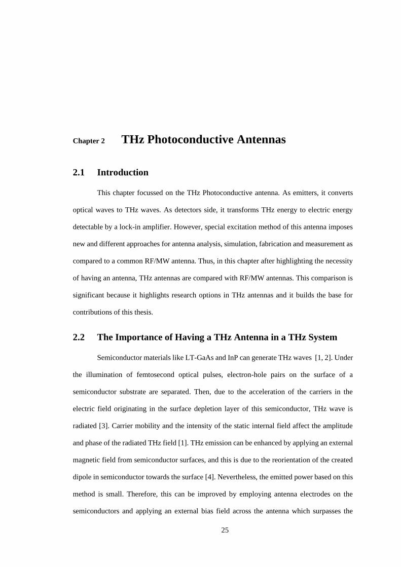
As shown in Fig. 2.1, an antenna electrode can have various shapes and geometries.
Commonly used in THz pulsed systems due to their frequency independent characteristics are
the bowtie antennas. Furthermore, the sharp ends of the antenna lead to singular electric fields
hence enhancing the THz radiation from the device [15]. Besides bowtie antennas, a large gap
coplanar strip line is also favoured because it does not need micro-fabrication techniques like
small gap antennas. Also, for a precise laser focus alignment, a large gap coplanar strip line is
not as sensitive as small gap antennas.
27
(a) (b)
Fig. 2.1 Sketch of THz photoconductive antennas (a) small gap bowtie antenna (b) large-aperture
coplanar strip line [10]
2.3.1 Theoretical Principle of THz Photoconductive Antenna as an Emitter
Electron-hole pairs are created when the THz photoconductive antenna as an emitter is
excited by ultra-short laser pulses. These ultra-short laser pulse’s photon energy is higher than
the bandgap energy of semiconductor material. Due to the bias voltage across the electrodes of
the antenna, transient photocurrents are produced, because of the acceleration and deceleration
of the photo-generated carriers. As a result, the THz wave is radiated into free space by the
antenna. The theory of generation of THz photocurrent may differ [11] from each other due to
the differences in the antenna gap size. In the following section, this is discussed in detail.
2.3.1.1 Large-Aperture Antennas
The emission of THz radiation from the large-aperture antenna is in line with the theory
of dipole antenna. The generated photocurrent can be assumed as surface current confined to a
thin layer in the photoconductive gap [11, 16-17] under the laser illumination. Hence, the on–
axis radiated THz field in the temporal format can be written as [17]:
(2.1)
where is the surface current density, µ is the permeability, S is the photo-excited area in
the antenna gap and z is the on-axis distance from the antenna gap.
According to the detailed explanations in Appendix A, the surface current density in a
large-aperture antenna is:
dt
tJd
z
S
r
dS
t
tJtrE ss
THz)(
4
)(
4),(
)(tJs
28
(2.2)
where is the surface conductivity of the photoconductive substrate, m* is the
effective mass and μe is the electron mobility and related to photoconductive material
characteristics as .
Through equations 2.1 and 2.2, the radiated THz field can be obtained as:
(2.3)
Hence, it can be interpreted that large aperture antennas relied on surface current density and
applied bias to antenna electrodes.
2.3.1.2 Small Gap Antennas
While the emission of THz radiation from a large-aperture antenna is in line with the
theory of dipole antenna, the emission of THz radiation from a small gap antenna is in line with
the theory of Hertzian dipole. The radiated electric field is proportional to the time derivative
of the current, Ipc, (or equivalently it is proportional to the current density, Jpc) as [18, 19]:
(2.4)
The movement of electrons from the valence band to the conduction band under the
laser illumination generated the photocurrent. Since the electron (free carrier) density in the
conduction band is n(t), and the velocity of carriers is v(t), the current density, Jpc (t) is given
by [20]:
(2.5)
Where e is the electron charge. This current relation applies to the hole, but with a positive sign.
Hole contribution to THz current and radiation is much smaller [21] due to the effective mass
of a hole is much larger than that of the electron; hence it is often be neglected.
11
)(
)()()(
0
r
s
biasss t
tEttJ
)()( tnet es
*me se
bias
r
e
e
bias
r
s
s
THz Etne
dt
tdne
z
SE
tdt
td
z
StzE
2020 )11
)((
)(
4)1
1
)((
)(
4),(
t
tJ
t
tItE
pcpcTHz
)()()(
)()()( tvtnetJ pc
29
A simple one-dimensional Drude-Lorentz model has been developed in [14] in order
to explain the main features of this photocurrent density and carrier dynamics. This model
consists of three interlinked differential equations describing the relation of free carrier density,
the velocity of carriers, and the polarisation caused by separated carriers under the bias field,
Psc. These equations are as follows:
(2.6)
(2.7)
(2.8)
(2.9)
Where τc is the carrier lifetime where it is the average time span that excess free electrons
survive before recombining [20], τs is the momentum relaxation time or carrier scattering time
where it is the average time between two collisions of each electron in the conduction band,
and it is in the order of a tenth of ps [20], τr is the carrier recombination lifetime [22], G(t) is
the generation rate of carriers by laser pulses, m* is the effective mass, Elocal is the electric field
in the photoconductive gap, Ebias is the applied bias to antenna electrodes, and ζ is the
geometrical factor [14]. Jpc(t) and ETHz(t) can be found through numerical calculations of
equations (2.6) -(2.9)
Radiated THz field can be related to carrier dynamics and calculated as:
(2.10)
by considering both equations (2.4) and (2.5)
Hence, it can be interpreted that for small gap antennas, THz radiation relies on the
results of ultrafast variation in carrier density and acceleration of photo-carriers. This THz
radiation can be increased by applying a large bias field and large optical power.
)()()(
tGtn
dt
tdn
c
locals
Em
etv
dt
tdv*
)()(
sc
biaslocalP
EE
)(tJP
dt
dPpc
r
scsc
dt
tdvtnetv
dt
tdne
t
tJtE
pcTHz
)()()(
)()()(
30
By comparing equations (2.3) for large-aperture antennas and (2.10) for small gap
antennas, it can be interpreted that different antenna gap sizes impose different analysis criteria
and different equations for the radiated THz field. The focus of this thesis is on small gap
antennas which are used in the proposed model in Chapter 5.
2.3.2 Theoretical Principle of a THz Photoconductive Antenna as a Detector
THz detection by photoconductive antennas is the opposite of the emitting process. No
bias voltage is applied across the electrodes in detection. The incident THz radiation induces a
voltage across the antenna which accelerates photo-carriers generated by the gating laser pulse
from the optical source. The arrival time of the gating pulse can be adjusted using a variable
time delay gating pulse thus the temporal behaviour of the photocurrent due to THz radiation
can be measured. The photocurrent can be measured by a current meter or lock-in amplifier
[10].
Based upon the Ohm’s law, the detected photocurrent at a time delay of t can be
explained as shown in the equation below as:
(2.11)
Where ETHz(t) is the received THz signal, σdet(t) is the time-varying conductivity of the detector,
and nr(t) is the generated photo-carrier density by the gating pulse [19]. For photoconductive
materials with ultra-short carrier lifetime , then the detected current from equation
(2.11) will be proportional to the original income THz signal where . For
materials with extremely long carrier lifetime like SI-GaAs, it is presumed that nr(t) has
behaviour like a step function then . This proves that the bandwidth of
the detected signal of affected by the characteristics of the photo-carrier density in the detector
antenna and its decay behaviour. The in-between case is the realistic situation where the
distortion effect of the detector on the incident THz field is considered by convolving the
detector response with THz field in time domain [21]. Thus, the detected photocurrent for the
tdttnetEttEtJ reTHzTHz )()()()()( detdet
)()( ttnr
)()(det fEfJ THz
ffEfJ THz )()(det
31
in-between situation can be explained considering the spectral behaviour of laser pulses, Il(f),
and carrier dynamics in the photoconductive antenna, B(f) as equation (2.12) [18, 23].
(2.12)
The amount of detected signal at high frequencies is determined by the response time
of the detector [10]. Other factors that determine the amount of detected signal are finite carrier
recombination lifetime of semiconductor, τr, and the RC time constant related to the device
capacitance [24]. Hence, THz photoconductive antenna in detector side can be construed as a
low pass filter dominated by carrier lifetime and carrier recombination time of photoconductive
material. Small gap photoconductive antennas are commonly employed as detectors. The
sensitivity of a detector reduces once the antenna gap size is increasing as the optical intensity
on the gap reduces [14]. The maximum response of detector shifts to lower frequencies also is
the outcome of a bigger antenna gap size [14].
2.4 Comparison of THz Antennas with RF/MW Antennas
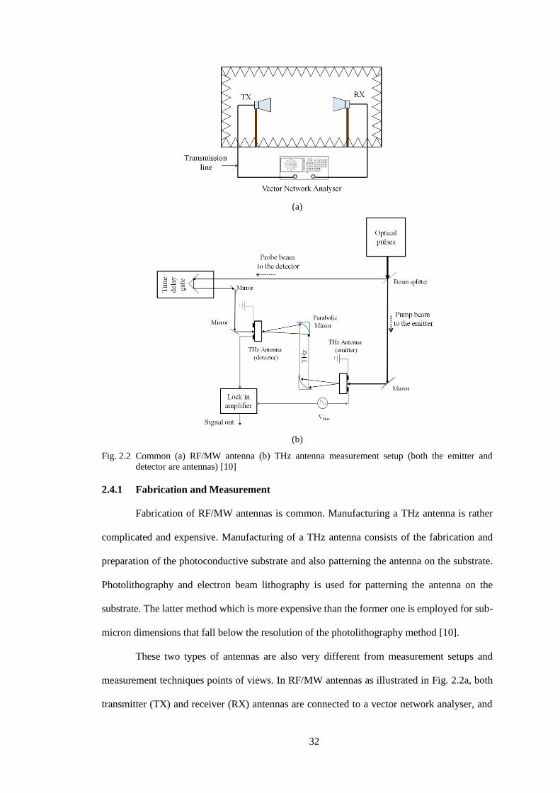
Fig. 2.2a and Fig. 2.2b show common RF/MW and THz antenna measurement setups
respectively [25, 26]. It is apparent that THz antennas differ significantly from the conventional
RF/MW antennas from the measurement facility, feeding method and antenna structure points
of views. These differences are elaborated and summarised in this section.
)()()()(det tEfBfIfJ THzl
32
(a)
(b)
Fig. 2.2 Common (a) RF/MW antenna (b) THz antenna measurement setup (both the emitter and
detector are antennas) [10]
2.4.1 Fabrication and Measurement
Fabrication of RF/MW antennas is common. Manufacturing a THz antenna is rather
complicated and expensive. Manufacturing of a THz antenna consists of the fabrication and
preparation of the photoconductive substrate and also patterning the antenna on the substrate.
Photolithography and electron beam lithography is used for patterning the antenna on the
substrate. The latter method which is more expensive than the former one is employed for sub-
micron dimensions that fall below the resolution of the photolithography method [10].
These two types of antennas are also very different from measurement setups and
measurement techniques points of views. In RF/MW antennas as illustrated in Fig. 2.2a, both
transmitter (TX) and receiver (RX) antennas are connected to a vector network analyser, and
33
the various parameters of the antenna under tests such as radiation pattern, gain, efficiency,
impedance/VSWR, bandwidth, and polarisation can be determined. The alignment of TX and
RX antennas is relatively easy. Measurement facilities for RF/MW antennas are known as
anechoic chambers and reverberation chambers. Antenna measurements can take on many
forms, including near-field and far-field measurements. A basic test system requires at least a
source antenna with a transmitter and the antenna under test with a receiver. The main idea in
this testing is to use the source antenna and a transmitter with suitable bandwidth and
polarisation to illuminate the antenna under test with plane waves, which can then be measured
by the receiver being fed by the antenna under test. One variation on this system involves a
switchable reference antenna for feeding the test receiver with known performance
characteristics. Another involves some kind of a positioning system to rotate the antenna under
test relative to the source antenna, thus measuring the radiation pattern as a function of angle.
In the THz measurement setup as shown in Fig. b, there is no physical connection
between the optical source and the emitter and/or detector antenna. Various optical components
such as parabolic mirrors are allocated between the emitter and detector antennas to direct the
electromagnetic wave which may attenuate and broaden the THz signal. From the shown setup
in Fig. 2.2b, the amplitude and phase of the THz signal can be detected. However, for pattern
measurement of the antenna, another setup using fibre coupled detectors is needed [27, 28] as
the antenna under test in the THz system cannot be rotated in contrast to RF/MW antennas as
the rotation will cause the loss of laser illumination on the THz antenna gap. Moreover, the
alignment of the THz system is a very sensitive task, and the detected THz signal is crucially
affected by it. Finally, as THz signals are sensitive to water vapours, it is better for THz
measurement bench to be in an enclosed environment and to be purged with dry nitrogen.
2.4.2 Feeding, Excitation Source and Biasing
Coplanar Waveguide (CPW), coaxial cable, and microstrip are among various feed
lines available for conventional antennas but, for a THz antenna, there is none. There are two
ways to couple the optical pulses to a THz antenna firstly through the air and secondly through
34
a fibre. Typically, optical waves are coupled to the antenna through the air. However, for some
industrial applications where flexible and movable emitters and detectors are essential, optical
fibres are employed. Recently some fibre-coupled THz systems have been presented for 800
nm laser pulses [29] and 1550 nm which are telecommunication wavelength pulses [30, 31].
The feed line for THz antennas is actually a laser; therefore, the source impedance of the
antenna is variable, and this is different to commonly used 50 Ohms feed lines of RF/MW
antennas.
Another difference between RF/MW and THz antennas are from bias voltage point of
view. RF/MW antennas do not need any biasing. However, as shown in Fig 2.2b, THz antennas
as emitters require voltage biasing as it is the fundamental procedure of THz generation. When
employed as a detector, THz antennas do not need bias voltage.
2.4.3 Electrode Material
Highly conductive metals such as copper and silver usually made RF/MW antennas. In
THz antennas, an AuGe alloy and a layer of Ti/Au (Titanium/Gold) are employed as the
electrode material. These are suitable metallization types on LT-GaAs substrates and can
provide ohmic contacts [32]. AuGe alloys such as AuGe/Ni/Au have been used in THz antennas
[33, 34]. However, Ti/Au (or Ti/Pd/Au) layer stack is more extensively employed [5,36-38]
where a thin layer of Ti is initially deposited to improve adhesion of the Au to the substrate
[39]. The advantage of the Ti/Au contact over the AuGe alloy is that for its deposition no
annealing is required and it is more thermally stable under laser illumination [32]. The electrical
conductivity, σ, of Au is 45.2 × 10⁶ S/m [16]. Most of the current flow occurs in a very thin
region near the surface of the conductor since the skin depth or characteristic depth of
penetration, for Au at 1 THz is 74.9 nm. The surface resistance, in this case, is
0.29 Ω. In practice for THz antennas, usually 10-20 nm thick Ti followed by Au with a thickness
of 100 nm is deposited on the photoconductive substrate.
Graphene is another type of material which very recently has been theoretically studied
as an antenna electrode material [40-41]. It is a one-atom-thick 2D carbon crystal which has
f1
35
extraordinary mechanical, electronic and optical properties [42] and has a Young modulus of
1.5 TPa, the carrier mobility of 200 000 cm2.V-1.s-1 [43], and an absorption coefficient of 24×104
cm-1 [44]. Various parameters such as temperature and chemical potential determine the surface
conductivity of graphene. The chemical potential of graphene is one of the parameters which
can be tuned to achieve antennas with different radiation characteristics thus realising
reconfigurable antennas [45].
2.4.4 Substrate Material
A low-loss dielectric material is desirable in planar RF/MW antennas. One of the most
common dielectric materials for this type of antennas is FR4 which consists of fibreglass
reinforced epoxy laminate sheet. Special MW antenna category, for example, monolithic
microwave integrated circuit (MMIC), however, needs GaAs as the main substrate material due
to its high carrier mobility and homogeneous nature [39, 46].
For THz antennas, the substrate material used is a photoconductive material which is
basically a semiconductor, such as Si, InP, GaAs, and InGaAs. LT-GaAs is the most popular
material due to its desirable characteristics, namely ultra-short carrier lifetime in order to obtain
fast current pulses or CW current variation, relatively high electron mobility in order to obtain
strong THz signals, high intrinsic resistivity and high breakdown voltage in order to support
applying high bias voltages [47-48]. Since photoconductive materials play a crucial role in THz
wave generation and detection, characteristics and effective parameters of them with the main
focus on LT-GaAs is described in the next sub-section.
One of the intensely studied topics in the THz field is the THz photoconductive
material. No natural material exists to allow an efficient and powerful THz emission, hence
spurred the interest [49]. The intrinsic carrier lifetime of materials is not fast enough to reach
very high frequency ranges of the THz spectrum. Thus, to reduce the carrier lifetime, material
studies for THz are very crucial and the research and improvement of material characteristics
for optoelectronic applications still ongoing [50, 51].
36
The first THz antenna developed in [52] used silicon as the photoconductive substrate
material. The bandgap of the silicon is 1.12 eV at 300 K, with corresponding intrinsic resistivity
of 2.3 × 10⁵ Ω.cm. However, the bandgap of silicon is indirect which means that the minimum
of conduction-band is misaligned compared to the maximum of valence-band [53]. This results
in a relatively slow optical recombination process.
GaAs, on the other hand, has a direct bandgap, and photon emission is possible without
phonon exchange with the lattice. The intrinsic resistivity of GaAs is 108 Ω.cm. As GaAs an
III-V compound, it is possible to modify its composition of alloys by adding defects to tune the
electrical and optical behaviours. Many development and improvement in characteristics of
GaAs is one of the main reason progress in THz antennas is possible [54]. GaAs crystal can be
grown in semi-insulating (SI) form by liquid encapsulated Czochralski (LEC) method. In this
process, all dependencies of GaAs on quartz and carbon components are eliminated [55]. This
forms a substrate where it is possible to grow another epitaxial layer.
The carrier lifetime of SI-GaAs is in the range of hundreds of picoseconds. This
satisfies the needs to have THz antennas with large bandwidth and good SNR. This may be
achieved by incorporating additional energy levels in the bandgap through various native point
defect types [47]. Therefore, another recombination path can be provided by trapping electrons
in intermediate states. For this purpose, point defects should be introduced into the crystal.
Adding defects can reduce carrier lifetime of the material which is desirable. On the other hand,
it reduces thermal conductivity and the carrier mobility because the mean free paths are
decreased as a result of new scattering centres introduced by trapping levels [20,56]. These
consequences are unfavourable. Hence, it can be concluded that the primary challenge in the
development of ultrafast photoconductive materials is to have material with a sub-picoseconds
carrier lifetime, high mobility and a high dark resistivity.
Low temperature growth technique in molecular beam epitaxy Molecular beam epitaxy
(MBE) is one of the conventional technique to introduce defects into the material. This method
produces LT-GaAs. Typically, at a low growth temperature between 200 to 250°C, GaAs is
deposited in excess of As which leads to the formation of a relatively high density of point

37
defects. Under an As overpressured at high annealing temperature typically between 500 and
600°C, it is annealed [48,57] to increase the resistivity. A 1 to 2 μm-thick LT-GaAs layer as the
active layer is usually grown on SI-GaAs [47].
LT-GaAs was first used in 1988 [58], and since then continuous research on the effect
of various growth and annealing factors on properties of LT-GaAs has been performed [57, 59-
61]. However, still in literature when a THz antenna on LT-GaAs is used, the full parameters
related to the production of the LT-GaAs wafer especially on its growth and its annealing
temperatures wafer and the derived carrier lifetime are discussed. Each MBE chamber is
unique, and even in the same chamber, it is challenging to replicate the same wafer’s
characteristics. This fabrication process is sensitive to the ambient condition, and the exact
growth temperature is difficult to control. Another parameter of the photoconductive material
influenced by the fabrication procedure is the material resistivity. The resistivity decreases with
the growth of the temperature [62]. Annealing process helps to increase this resistivity that was
effected before.
Other methods to modify the characteristics of GaAs have been practised like ion-
implantation [63] and use of self-assembled ErAs islands in GaAs [54, 64-65]. The objective
of these techniques is to create a similar material with a carrier lifetime mirroring LT-GaAs.
The results are ErAs: GaAs which has high resistivity but with low mobility and Ion-implanted
GaAs which has high mobility but with very low intrinsic resistivity. Hence, LT-GaAs is still
the best material for THz antennas [49].
Indium based is another category of photoconductive materials for THz applications is
from III-V compounds. These materials have narrower bandgap energy. The bandgap of
InGaAs is 0.75 eV compared to 1.43 eV of LT-GaAs. Thus, Indium based III-V compounds
are suitable materials at higher optical wavelengths. Ultra-short carrier lifetime and high
resistivity of LT-InGaAs had been reported in [51]. Most application for LT-InGaAs is in the
telecommunication wavelength of 1.55 um. Fibre amplifiers with high power, narrow line-
width and tunable wavelength in this frequency are also available [69]. Compatibility with 1.55
μm has been achieved with Fe-implanted InGaAs [70-71], ErAs: InGaAs [72], heavy-ion
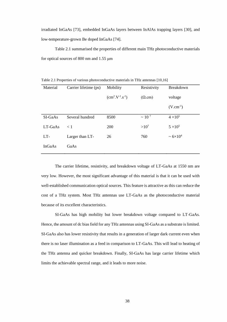
38
irradiated InGaAs [73], embedded InGaAs layers between InAlAs trapping layers [30], and
low-temperature-grown Be doped InGaAs [74].
Table 2.1 summarised the properties of different main THz photoconductive materials
for optical sources of 800 nm and 1.55 μm
Table 2.1 Properties of various photoconductive materials in THz antennas [10,16]
Material Carrier lifetime (ps) Mobility
(cm2.V-1.s-1)
Resistivity
(Ω.cm)
Breakdown
voltage
(V.cm-1)
SI-GaAs Several hundred 8500 ~ 10 7 4 ×10⁵
LT-GaAs < 1 200 >107 5 ×10⁵
LT-
InGaAs
Larger than LT-
GaAs
26 760 ~ 6×10⁴
The carrier lifetime, resistivity, and breakdown voltage of LT-GaAs at 1550 nm are
very low. However, the most significant advantage of this material is that it can be used with
well-established communication optical sources. This feature is attractive as this can reduce the
cost of a THz system. Most THz antennas use LT-GaAs as the photoconductive material
because of its excellent characteristics.
SI-GaAs has high mobility but lower breakdown voltage compared to LT-GaAs.
Hence, the amount of dc bias field for any THz antennas using SI-GaAs as a substrate is limited.
SI-GaAs also has lower resistivity that results in a generation of larger dark current even when
there is no laser illumination as a feed in comparison to LT-GaAs. This will lead to heating of
the THz antenna and quicker breakdown. Finally, SI-GaAs has large carrier lifetime which
limits the achievable spectral range, and it leads to more noise.

39
2.4.5 Type of Current
Conduction current due to the motion of conduction electrons is the current type in
RF/MW. In THz antennas however the generation of current in the photoconductive material
is attributed to two phenomena which are the generation of electron-hole pairs under electric
bias field known as drift current and displacement current which is due to second order
nonlinear optical characteristics of the photoconductive substrate. However, the effect of the
displacement current is only considered at low bias fields. At high bias fields (more than 105
V.cm-1) drift current is dominant [14, 75]. More details on the current type are discussed in
Chapter 4.
2.4.6 Computer Aided Design
There is no available and complete design tool available for THz antenna designs
though Computer Aided Design (CAD) is now a common practice for conventional antenna
designs. Generation of THz waves from the antennas consists of two processes which are
optoelectronic and electromagnetic (EM) parts. Most available commercial tools can only
simulate the first or second part of the process. No readymade commercial software is dedicated
to the THz antenna. Therefore, the development of a new method that can facilitate analysis of
THz antennas by combining numerical and CAD method is required. This is the main
contributions of this thesis that will be explained in Chapter 5.
To sum up, the significant differences between these two types of antennas are
reviewed in Table 2.2. The dissimilarities highlight the necessity of having a different analysis
approach for THz antennas.
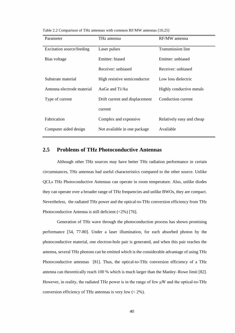
40
Table 2.2 Comparison of THz antennas with common RF/MW antennas [10,25]
Parameter THz antenna RF/MW antenna
Excitation source/feeding Laser pulses Transmission line
Bias voltage Emitter: biased
Receiver: unbiased
Emitter: unbiased
Receiver: unbiased
Substrate material High resistive semiconductor Low loss dielectric
Antenna electrode material AuGe and Ti/Au Highly conductive metals
Type of current Drift current and displacement
current
Conduction current
Fabrication Complex and expensive Relatively easy and cheap
Computer aided design Not available in one package Available
2.5 Problems of THz Photoconductive Antennas
Although other THz sources may have better THz radiation performance in certain
circumstances, THz antennas had useful characteristics compared to the other source. Unlike
QCLs THz Photoconductive Antennas can operate in room temperature. Also, unlike diodes
they can operate over a broader range of THz frequencies and unlike BWOs, they are compact.
Nevertheless, the radiated THz power and the optical-to-THz conversion efficiency from THz
Photoconductive Antenna is still deficient (<2%) [76].
Generation of THz wave through the photoconduction process has shown promising
performance [54, 77-80]. Under a laser illumination, for each absorbed photon by the
photoconductive material, one electron-hole pair is generated, and when this pair reaches the
antenna, several THz photons can be emitted which is the considerable advantage of using THz
Photoconductive antennas [81]. Thus, the optical-to-THz conversion efficiency of a THz
antenna can theoretically reach 100 % which is much larger than the Manley–Rowe limit [82].
However, in reality, the radiated THz power is in the range of few μW and the optical-to-THz
conversion efficiency of THz antennas is very low (< 2%).
41
The entire wave generation process from a THz antenna needs to be considered in order
to have a better view and to understand the reason for having a low power level and efficiency.
For this purpose, the adopted method here is to divide the process into three parts [16, 25]:
1) Generation of THz photocurrent from optical power in the photoconductive material.
The related efficiency; i.e. optical-to-electrical efficiency, η1, can be defined as the ratio of the
generated THz power in the photoconductive gap to the optical power
2) The amount of coupled THz power from the photoconductive gap to the antenna
electrodes; i.e. matching efficiency, η2
3) The amount of coupled THz wave from the antenna to the free space; i.e. radiation
efficiency, η3.
The first two parts are different for THz antennas in a pulsed and a CW system due to
the excitation type, and they are separately described in the next sections. However, the latter
part; i.e. radiation efficiency, for both systems is the same, and it depends on the antenna
radiation characteristics- mainly the electrical thickness of the substrate and the relative
permittivity of photoconductive material. Since the photoconductive substrate has high
permittivity (εr = 12.9 for GaAs), as substrate thickness increases, the radiation efficiency
decreases sharply depending on substrate thickness. This is due to the generation of surface
waves.
2.5.1 Problems Related to THz Photoconductive Antennas
In order to find out how part one and two of the THz generation process contribute to
the optical-to-THz efficiency, a preliminary and straightforward calculation with approximate
assumptions is performed for a THz photoconductive antenna in a pulsed system [85].
1. The average photocurrent [86], Iavp, and approximate photoconductive resistance
[87], Rapp, are considered as equations (2.13) and (2.14) respectively:
(2.11)
2hfL
PVeI avbiasceavp
42
(2.12)
where Vbias is the bias voltage, L is the antenna gap length, and Pav is the average optical power.
Then, the optical-to-electrical efficiency can be estimated as:
(2.13)
The index of “p” is added to represent THz photoconductive antenna in a pulsed system.
Considering some typical values as μe = 1000 cm2.V-1.s-1, c = 0.5 ps, Vbias = 30 V, Pav = 50
mW, L = 5 μm, trep = 1/80 μs, and f = 375 THz and plugging in these values in equation (2.13),
η1p = 7.2 × 10⁻⁵.
2. The matching efficiency can be calculated according to equation (2.14) for a half-
wavelength dipole antenna on a substrate with εr = 12.9. Assuming the antenna resistance in
free space, Zfree, is 73 Ω and by using the above values in equation (2.12) Rapp is 0.89 Ω, then
the matching efficiency will be η2p = 0.16.
(2.14)
The total antenna efficiency for this sample, which is a multiplication of efficiencies
from described processes, is calculated as 5.7 × 10⁻⁶ [88]. Although this value is comparable
with what most people obtained in practice, it is smaller than some reported best efficiencies.
This could be due to better parameters realised in the best cases [88]. The details calculations
can be found in Appendix B.
2.6 Previous work on THz Photoconductive Antennas
Some previous research published had been focused on specific criteria to make
improvement in the radiated THz antenna performance and also efficiency. This section will
discuss the notable contribution done by the researchers.
repaveapp
tPe
hfLR
2
3 2
2
222
12
3
hfLt
Ve
P
IR
rep
biasce
av
avpappp
2
2 1apprfree
apprfreep
RZ
RZ

43
2.6.1 Varying Antenna Gap Area Geometry
Commonly used THz antennas are bowtie, dipole and coplanar strip line. Antenna gap
area is essential as it is where the electron-hole pairs are generated and coupled to the antenna
electrodes. Demonstrated in [12, 15, 33] antennas with sharp tip ends can produce larger THz
power compared to the antennas with rectangular edges in the gap. Sharper antenna tips, will
results in enhanced THz emission even with less optical power due to the overlapping of the
laser spot and the electric field area in the antenna gap. Though the fabrication of tiny sharp
tips for small gap antennas is difficult in reality, the importance of the geometry of the electrode
should not be undermined.
2.6.2 Improving Optical Power Coupling
Higher photo-carrier density and transient photocurrent can be achieved by increasing
the absorption of infrared laser power to the antenna. In order to increase the absorption, anti-
reflection (AR) coating Si3N4 is used on the antenna electrode. The coating is essentially an
optically transparent layer [128]. The reflection of optical waves from the surface of the device
will be suppressed with the existing of the additional layer. An AR with a refractive index of
, where nGaAs is the refractive index of the photoconductive material is usually used.
Another approach is to use AlAs: GaAs or AlAs: AlGaAs Bragg reflectors [54,89]. This
material acts as a mirror for optical waves, and it is transparent to THz waves. It is located
beneath the active layer of a substrate. Fig. 2.3 shows the schematic view of an antenna with
both an AR coating and Bragg reflectors.
GaAsn
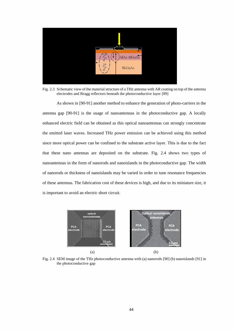
44
Fig. 2.3 Schematic view of the material structure of a THz antenna with AR coating on top of the antenna
electrodes and Bragg reflectors beneath the photoconductive layer [89]
As shown in [90-91] another method to enhance the generation of photo-carriers in the
antenna gap [90-91] is the usage of nanoantennas in the photoconductive gap. A locally
enhanced electric field can be obtained as this optical nanoantennas can strongly concentrate
the emitted laser waves. Increased THz power emission can be achieved using this method
since more optical power can be confined to the substrate active layer. This is due to the fact
that these nano antennas are deposited on the substrate. Fig. 2.4 shows two types of
nanoantennas in the form of nanorods and nanoislands in the photoconductive gap. The width
of nanorods or thickness of nanoislands may be varied in order to tune resonance frequencies
of these antennas. The fabrication cost of these devices is high, and due to its miniature size, it
is important to avoid an electric short circuit.
(a) (b)
Fig. 2.4 SEM image of the THz photoconductive antenna with (a) nanorods [90] (b) nanoislands [91] in
the photoconductive gap

45
In [92], nano-structuring of metals or nanoplasmonic electrodes is another cutting edge
technology introduced in order to improve the coupling of optical power to the antenna and the
THz radiated power. The main goal is to reduce the photo-carrier transport time, and this can
be done by employing arrays of sub-micron electrodes. Due to the coupling of light with the
surface plasmon of the sub-wavelength arrays, the interaction and concentration of the emitted
wave on noble metals for example gold are increased [93]. Here, surface plasmon is introduced
as collective oscillation of free electrons at the boundary between a conductor and a dielectric
material.
Also using this concept, an array of dipole antennas with plasmonic contacts has been
reported by [69] as shown in Fig. 2.5.Ultra-short THz pulses with superior responsivity have
been achieved from this device as an emitter, even though the antenna was mounted on large
electron mobility and large carrier lifetime material. This is due to the short carrier transport
time provided by electrodes and increased transmission of laser power to the sub-wavelength
gaps of electrodes because of surface plasmon waves.
Fig. 2.5 SEM image of plasmonic THz dipole arrays, a middle ground electrode is added to collect the
remaining electron-holes in the antenna gap quicker to prevent the screening effect [69]
A small gap dipole antenna with nanoplasmonic interdigitated fingers on SI-GaAs as
shown in Fig. 2.6 [94] were also introduced. Nano distance gaps (100 nm) allows coupling of
generated photo-carriers to the antenna more efficiently due to reducing transport distance. This
geometry, however, is prone to break down at high optical powers due to narrow distance
between the fingers.
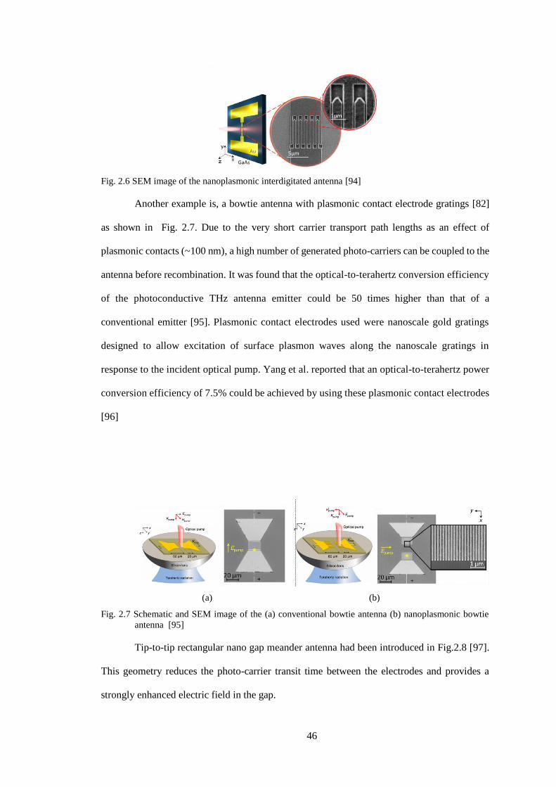
46
Fig. 2.6 SEM image of the nanoplasmonic interdigitated antenna [94]
Another example is, a bowtie antenna with plasmonic contact electrode gratings [82]
as shown in Fig. 2.7. Due to the very short carrier transport path lengths as an effect of
plasmonic contacts (~100 nm), a high number of generated photo-carriers can be coupled to the
antenna before recombination. It was found that the optical-to-terahertz conversion efficiency
of the photoconductive THz antenna emitter could be 50 times higher than that of a
conventional emitter [95]. Plasmonic contact electrodes used were nanoscale gold gratings
designed to allow excitation of surface plasmon waves along the nanoscale gratings in
response to the incident optical pump. Yang et al. reported that an optical-to-terahertz power
conversion efficiency of 7.5% could be achieved by using these plasmonic contact electrodes
[96]
(a) (b)
Fig. 2.7 Schematic and SEM image of the (a) conventional bowtie antenna (b) nanoplasmonic bowtie
antenna [95]
Tip-to-tip rectangular nano gap meander antenna had been introduced in Fig.2.8 [97].
This geometry reduces the photo-carrier transit time between the electrodes and provides a
strongly enhanced electric field in the gap.
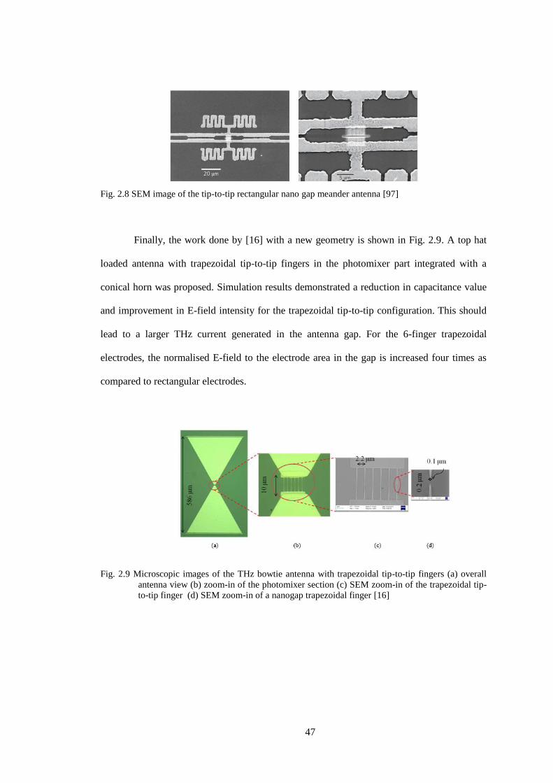
47
Fig. 2.8 SEM image of the tip-to-tip rectangular nano gap meander antenna [97]
Finally, the work done by [16] with a new geometry is shown in Fig. 2.9. A top hat
loaded antenna with trapezoidal tip-to-tip fingers in the photomixer part integrated with a
conical horn was proposed. Simulation results demonstrated a reduction in capacitance value
and improvement in E-field intensity for the trapezoidal tip-to-tip configuration. This should
lead to a larger THz current generated in the antenna gap. For the 6-finger trapezoidal
electrodes, the normalised E-field to the electrode area in the gap is increased four times as
compared to rectangular electrodes.
Fig. 2.9 Microscopic images of the THz bowtie antenna with trapezoidal tip-to-tip fingers (a) overall
antenna view (b) zoom-in of the photomixer section (c) SEM zoom-in of the trapezoidal tip-
to-tip finger (d) SEM zoom-in of a nanogap trapezoidal finger [16]
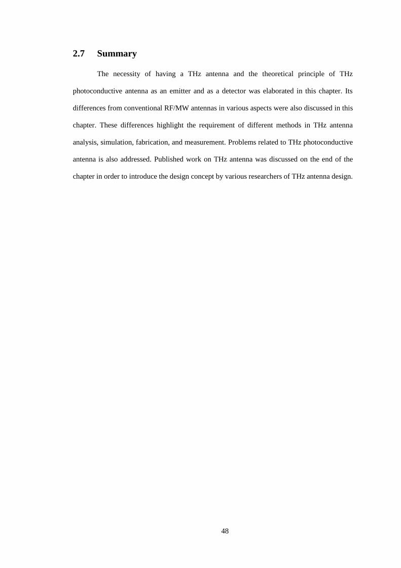
48
2.7 Summary
The necessity of having a THz antenna and the theoretical principle of THz
photoconductive antenna as an emitter and as a detector was elaborated in this chapter. Its
differences from conventional RF/MW antennas in various aspects were also discussed in this
chapter. These differences highlight the requirement of different methods in THz antenna
analysis, simulation, fabrication, and measurement. Problems related to THz photoconductive
antenna is also addressed. Published work on THz antenna was discussed on the end of the
chapter in order to introduce the design concept by various researchers of THz antenna design.
49
References
[1] X. C. Zhang, B. B. Hu, J. T. Darrow, and D. H. Auston, "Generation of femtosecond
electromagnetic pulses from semiconductor surfaces," Applied Physics Letters, vol.
56, pp. 1011-1013, 1990.
[2] M. Johnston, D. Whittaker, A. Corchia, A. Davies, and E. Linfield, "Simulation of
terahertz generation at semiconductor surfaces," Physical Review B, vol. 65, 2002.
[3] C. Weiss, R. Wallenstein, and R. Beigang, "Magnetic-field-enhanced generation of
terahertz radiation in semiconductor surfaces," Applied Physics Letters, vol. 77, pp.
4160-4162, 2000.
[4] M. B. Johnston, D. M. Whittaker, A. Corchia, A. G. Davies, and E. H. Linfield,
"Theory of magnetic-field enhancement of surface-field terahertz emission," Journal
of Applied Physics, vol. 91, pp. 2104-2106, 2002.
[5] I. S. Gregory, C. Baker, W. R. Tribe, I. V. Bradley, M. J. Evans, E. H. Linfield, A. G.
Davies, and M. Missous, "Optimization of photomixers and antennas for continuous-
wave terahertz emission," IEEE Journal of Quantum Electronics, vol. 41, pp. 717-
728, 2005.
[6] http://www.thorlabs.co.uk/newgrouppage9.cfm?objectgroup_id=4716.
[7] http://www.toptica.com/products/terahertz_generation/fs_packages/photoconductive
switches.html
[8] http://www.tetechs.com/.
[9] http://www.menlosystems.com/products/?families=77
[10] Y. Lee, Principles of Terahertz science and technology, 1st ed. New York, NY:
Springer, 2008.
[11] J. T. Darrow, Z. Xi-Cheng, D. H. Auston, and J. D. Morse, "Saturation properties of
large-aperture photoconducting antennas," IEEE Journal of Quantum Electronics,
vol. 28, pp. 1607-1616, 1992.

50
[12] M. R. Stone, M. Naftaly, R. E. Miles, J. R. Fletcher, and D. P. Steenson, "Electrical
and radiation characteristics of semilarge photoconductive terahertz emitters," IEEE
Transactions on Microwave Theory and Techniques, vol. 52, pp. 2420-2429, 2004.
[13] G. Zhao, R. N. Schouten, N. v. d. Valk, W. T. Wenckebach, and P. C. M. Planken,
"Design and performance of a THz emission and detection setup based on a semi-
insulating GaAs emitter," Review of Scientific Instruments, vol. 73, pp. 1715-1719,
2002.
[14] P. U. Jepsen, R. H. Jacobsen, and S. R. Keiding, "Generation and detection of terahertz
pulses from biased semiconductor antennas," J. Opt. Soc. Am. B, vol. 13, pp. 2424-
2436, 1996.
[15] Y. Cai, I. Brener, J. Lopata, J. Wynn, L. Pfeiffer, and J. Federici, "Design and
performance of singular electric field terahertz photoconducting antennas," Applied
Physics Letters, vol. 71, pp. 2076-2078, 1997.
[16] N. Khiabani, “Modelling, design and characterisation of Terahertz photoconductive
antenna”. PhD thesis, Department of Electrical and Electronics Engineering,
University of Liverpool, 2013.
[17] P. K. Benicewicz, J. P. Roberts, and A. J. Taylor, "Scaling of terahertz radiation from
large-aperture biased photoconductors," J. Opt. Soc. Am. B, vol. 11, pp. 2533-2546,
1994.
[18] P. U. Jepsen, D. G. Cooke, and M. Koch, "Terahertz spectroscopy and imaging –
Modern techniques and applications," Laser & Photonics Reviews, vol. 5, pp. 124-
166, 2011.
[19] K. Sakai, Terahertz optoelectronics, 1st ed. Berlin: Springer 2005.
[20] J. Colinge and C. A. Colinge, Physics of semiconductor devices. Boston: Kluwer
Academic Publishers, 2002.
[21] Z. Piao, M. Tani, and K. Sakai, "Carrier Dynamics and Terahertz Radiation in
Photoconductive Antennas," Jpn. J. Appl. Phys., vol. 39, pp. 96-100, 2000.

51
[22] S. D. Brorson, J. Zhang, and S. R. Keiding, "Ultrafast carrier trapping and slow
recombination in ion-bombarded silicon on sapphire measured via THz
spectroscopy," Applied Physics Letters, vol. 64, pp. 2385-2387, 1994.
[23] L. Duvillaret, F. Garet, J. F. Roux, and J. L. Coutaz, "Analytical modelling and
optimisation of terahertz time-domain spectroscopy experiments, using photoswitches
as antennas," IEEE Journal of Selected Topics in Quantum Electronics, vol. 7, pp.
615-623, 2001.
[24] S. Kono, M. Tani, P. Gu, and K. Sakai, "Detection of up to 20 THz with a low-
temperature-grown GaAs photoconductive antenna gated with 15 fs light pulses,"
Applied Physics Letters, vol. 77, pp. 4104-4106, 2000.
[25] Y. Huang, N. Khiabani, S. Shen, and L. Di, "Terahertz photoconductive antenna
efficiency," in 2011 International Workshop on Antenna Technology (iWAT), 2011,
pp. 152-156.
[26] N. Khiabani, Y. Huang, Y. Shen, and S. Boyes, "Theoretical Modeling of a
Photoconductive Antenna in a Terahertz Pulsed System," IEEE Transactions on
Antennas and Propagation, vol. PP, pp. 1-1, 2013.
[27] J. Klier, S. Wohnsiedler, W. Zouaghi, E. Peytavit, J. Lampin, J. Jonuscheit, and R.
Beigang, "Far-field THz radiation pattern from photoconductive emitters on different
substrates," in 36th International Conference on Infrared, Millimeter and Terahertz
Waves (IRMMW-THz), 2011 2011, pp. 1-2.
[28] J. Van Rudd and D. M. Mittleman, "Influence of substrate-lens design in terahertz
time-domain spectroscopy," J. Opt. Soc. Am. B, vol. 19, pp. 319-329, 2002.
[29] F. Ellrich, T. Weinland, D. Molter, J. Jonuscheit, and R. Beigang, "Compact fibre-
coupled terahertz spectroscopy system pumped at 800 nm wavelength," Review of
Scientific Instruments, vol. 82, p. 053102, 2011.
[30] B. Sartorius, H. Roehle, H. Künzel, J. Böttcher, M. Schlak, D. Stanze, H. Venghaus,
and M. Schell, "All-fiber terahertz time-domain spectrometer operating at 1.5 um
telecom wavelengths," Opt. Express, vol. 16, pp. 9565-9570, 2008.
52
[31] S. Han, H. Ko, N. Kim, H. Ryu, C. Wook Lee, Y. Ahn Leem, D. Lee, M. Yong Jeon,
S. Kyu Noh, H. Sook Chun, and K. Hyun Park, "Optical fibre-coupled InGaAs-based
terahertz time-domain spectroscopy system," Opt. Lett., vol. 36, pp. 3094-3096, 2011.
[32] N. Vieweg, M. Mikulics, M. Scheller, K. Ezdi, R. Wilk, H. W. Hübers, and M. Koch,
"Impact of the contact metallization on the performance of photoconductive THz
antennas," Opt. Express, vol. 16, pp. 19695-19705, 2008.
[33] M. Tani, S. Matsuura, K. Sakai, and S.-i. Nakashima, "Emission characteristics of
photoconductive antennas based on low-temperature-grown GaAs and semi-
insulating GaAs," Appl. Opt., vol. 36, pp. 7853-7859, 1997.
[34] S. Matsuura, M. Tani, and K. Sakai, "Generation of coherent terahertz radiation by
photomixing in dipole photoconductive antennas," Applied Physics Letters, vol. 70,
pp. 559-561, 1997.
[35] Y. C. Shen, P. C. Upadhya, H. E. Beere, E. H. Linfield, A. G. Davies, I. S. Gregory,
C. Baker, W. R. Tribe, and M. J. Evans, "Generation and detection of ultrabroadband
terahertz radiation using photoconductive emitters and receivers," Applied Physics
Letters, vol. 85, pp. 164-166, 2004.
[36] Y. Gao, M. Chen, S. Yin, P. Ruffin, C. Brantley, and E. Edwards, "Terahertz
enhancement from terahertz-radiation-assisted large aperture photoconductive
antenna," Journal of Applied Physics, vol. 109, p. 033108, 2011.
[37] S. Verghese, K. A. McIntosh, S. Calawa, W. F. Dinatale, E. K. Duerr, and K. A.
Molvar, "Generation and detection of coherent terahertz waves using two
photomixers," Applied Physics Letters, vol. 73, pp. 3824-3826, 1998.
[38] D. L. Woolard, R. Brown, M. Pepper, and M. Kemp, "Terahertz Frequency Sensing
and Imaging: A Time of Reckoning Future Applications?," Proceedings of the IEEE,
vol. 93, pp. 1722-1743, 2005.
[39] D. M. Pozar, Microwave engineering, 4th ed. Hoboken, NJ: Wiley, 2012.
53
[40] M. Tamagnone, J. S. Gomez-Diaz, J. R. Mosig, and J. Perruisseau-Carrier, "Analysis
and design of terahertz antennas based on plasmonic resonant graphene sheets,"
Journal of Applied Physics, vol. 112, p. 114915, 2012.
[41] I. Llatser, C. Kremers, A. Cabellos-Aparicio, J. M. Jornet, E. Alarcón, and D. N.
Chigrin, "Graphene-based nano-patch antenna for terahertz radiation," Photonics and
Nanostructures - Fundamentals and Applications, vol. 10, pp. 353-358, 2012.
[42] A. K. Geim and K. S. Novoselov, "The rise of graphene," Nat Mater, vol. 6, pp. 183-
191, 2007.
[43] M. Dragoman, A. A. Muller, D. Dragoman, F. Coccetti, and R. Plana, "Terahertz
antenna based on graphene," Journal of Applied Physics, vol. 107, p. 104313, 2010.
[44] B. Heshmat, H. Pahlevaninezhad, T. E. Darcie, and C. Papadopoulos, "Evaluation of
carbon nanotubes for THz photomixing," in 2010 IEEE Radar Conference, 2010, pp.
1176-1179.
[45] M. Tamagnone, J. S. Gomez-Diaz, J. R. Mosig, and J. Perruisseau-Carrier,
"Reconfigurable terahertz plasmonic antenna concept using a graphene stack,"
Applied Physics Letters, vol. 101, p. 214102, 2012.
[46] D. Singh, C. Kalialakis, P. Gardner, and P. S. Hall, "Small H-shaped antennas for
MMIC applications," IEEE Transactions on Antennas and Propagation, vol. 48, pp.
1134-1141, 2000.
[47] S. Gupta, J. F. Whitaker, and G. A. Mourou, "Ultrafast carrier dynamics in III-V
semiconductors grown by molecular-beam epitaxy at very low substrate
temperatures," IEEE Journal of Quantum Electronics, vol. 28, pp. 2464-2472, 1992.
[48] S. Gupta, M. Y. Frankel, J. A. Valdmanis, J. F. Whitaker, G. A. Mourou, F. W. Smith,
and A. R. Calawa, "Subpicosecond carrier lifetime in GaAs grown by molecular beam
epitaxy at low temperatures," Applied Physics Letters, vol. 59, pp. 3276-3278, 1991.
[49] M. Martin and E. R. Brown, "Critical comparison of GaAs and InGaAs THz
photoconductors," pp. 826102-826102, 2012.
54
[50] I. Kostakis, D. Saeedkia, and M. Missous, "Characterization of low temperature
InGaAs-InAlAs semiconductor photo mixers at 1.55 mu wavelength illumination for
terahertz generation and detection," Journal of Applied Physics, vol. 111, p. 103105,
2012.
[51] C. Baker, I. S. Gregory, W. R. Tribe, I. V. Bradley, M. J. Evans, E. H. Linfield, and
M. Missous, "Highly resistive annealed low-temperature-grown InGaAs with sub-500
fs carrier lifetimes," Applied Physics Letters, vol. 85, pp. 4965-4967, 2004.
[52] D. H. Auston, K. P. Cheung, and P. R. Smith, "Picosecond photoconducting Hertzian
dipoles," Applied Physics Letters, vol. 45, pp. 284-286, 1984.
[53] S. M. Sze and K. K. Ng, Physics of semiconductor devices, 3rd ed. Hoboken, N.J.:
Wiley-Interscience, 2007.
[54] Z. D. Taylor, E. R. Brown, J. E. Bjarnason, M. P. Hanson, and A. C. Gossard,
"Resonant-optical-cavity photoconductive switch with 0.5% conversion efficiency
and 1.0W peak power," Opt. Lett., vol. 31, pp. 1729-1731, 2006.
[55] L. Hrivank, "Semi-insulating GaAs," Czech. J. Phys. B, vol. 34, pp. 436-444, 1984.
[56] A. W. Jackson, J. P. Ibbetson, A. C. Gossard, and U. K. Mishra, "Reduced thermal
conductivity in low-temperature-grown GaAs," Applied Physics Letters, vol. 74, pp.
2325-2327, 1999.
[57] I. S. Gregory, C. Baker, W. R. Tribe, M. J. Evans, H. E. Beere, E. H. Linfield, A. G.
Davies, and M. Missous, "High resistivity annealed low-temperature GaAs with 100
fs lifetimes," Applied Physics Letters, vol. 83, pp. 4199-4201, 2003.
[58] F. W. Smith, H. Q. Le, V. Diadiuk, M. A. Hollis, A. R. Calawa, S. Gupta, M. Frankel,
D. R. Dykaar, G. A. Mourou, and T. Y. Hsiang, "Picosecond GaAs-based
photoconductive optoelectronic detectors," Applied Physics Letters, vol. 54, pp. 890-
892, 1989.
[59] J. K. Luo, H. Thomas, D. V. Morgan, D. Westwood, and R. H. Williams, "The
electrical breakdown properties of GaAs layers grown by molecular beam epitaxy at
low temperature," Semiconductor Science and Technology, vol. 9, p. 2199, 1994.
55
[60] R. Yano, Y. Hirayama, S. Miyashita, H. Sasabu, N. Uesugi, and S. Uehara, "Pump–
probe spectroscopy of low-temperature grown GaAs for carrier lifetime estimation:
arsenic pressure dependence of carrier lifetime during MBE crystal growth," Physics
Letters A, vol. 289, pp. 93-98, 2001.
[61] M. Missous, "Stoichiometric low temperature (SLT) GaAs and AlGaAs grown by
molecular beam epitaxy," Microelectronics Journal, vol. 27, pp. 393-409, 1996.
[62] H. Nemec, A. Pashkin, P. Kuzel, M. Khazan, S. Schnull, and I. Wilke, "Carrier
dynamics in low-temperature grown GaAs studied by terahertz emission
spectroscopy," Journal of Applied Physics, vol. 90, pp. 1303-1306, 2001.
[63] T. Liu, M. Tani, M. Nakajima, M. Hangyo, and C. Pan, "Ultrabroadband terahertz
field detection by photoconductive antennas based on multi-energy arsenic-ion-
implanted GaAs and semi-insulating GaAs," Applied Physics Letters, vol. 83, pp.
1322-1324, 2003.
[64] J. E. Bjarnason, T. L. J. Chan, A. W. M. Lee, E. R. Brown, D. C. Driscoll, M. Hanson,
A. C. Gossard, and R. E. Muller, "ErA s:GaAs photomixer with two-decade tunability
and 12 mu W peak output power," Applied Physics Letters, vol. 85, pp. 3983-3985,
2004.
[65] C. Kadowa and e. al, "Self-assembled ErAs islands in GaAs for THz applications,"
Physica E vol. 7, pp. 97-100, 2000.
[66] A. Krotkus, R. Viselga, K. Bertulis, V. Jasutis, S. Marcinkevicius, and U. Olin,
"Subpicosecond carrier lifetimes in GaAs grown by molecular beam epitaxy at low
substrate temperature," Applied Physics Letters, vol. 66, pp. 1939-1941, 1995.
[67] M. Tani and e. al, "Spectroscopicharacterisationn of Low-temperature- Grown GaAs
epitaxial films," Jpn. J. Appl. Phys., vol. 33, pp. 4807-4811, 1994.
[68] P. A. Loukakos, C. Kalpouzos, I. E. Perakis, Z. Hatzopoulos, M. Logaki, and C.
Fotakis, "Ultrafast electron trapping times in low-temperature-grown gallium
56
arsenide: The effect of the arsenic precipitate spacing and size," Applied Physics
Letters, vol. 79, pp. 2883-2885, 2001.
[69] C. Berry and M. Jarrahi, "Terahertz generation using plasmonic photoconductive
gratings," New Journal of Physics, vol. 14, p. 105029, 2012.
[70] M. Suzuki and M. Tonouchi, "Fe-implanted InGaAs photoconductive terahertz
detectors triggered by 1.56 mu m femtosecond optical pulses," Applied Physics
Letters, vol. 86, p. 163504, 2005.
[71] C. D. Wood, O. Hatem, J. E. Cunningham, E. H. Linfield, A. G. Davies, P. J. Cannard,
M. J. Robertson, and D. G. Moodie, "Terahertz emission from metal-organic
chemicavapouror deposition grown F e:InGaAs using 830 nm to 1.55 mu m
excitation," Applied Physics Letters, vol. 96, p. 194104, 2010.
[72] M. Sukhotin, E. R. Brown, D. Driscoll, M. Hanson, and A. C. Gossard, "Picosecond
photocarrier-lifetime in ErAs.
[73] J. Mangeney and P. Crozat, "Ion-irradiated In0.53Ga0.47As photoconductive
antennas for THz generation and detection at 1.55 μm wavelength," Comptes Rendus
Physique, vol. 9, pp. 142-152, 2008.
[74] A. Takazato, M. Kamakura, T. Matsui, J. Kitagawa, and Y. Kadoya, "Terahertz wave
emission and detection using photoconductive antennas made on low-temperature-
grown InGaAs with 1.56 mu m pulse excitation," Applied Physics Letters, vol. 91, p.
011102, 2007.
[75] B. B. Hu, A. S. Weling, D. H. Auston, A. V. Kuznetsov, and C. J. Stanton, "dc-
electric-field dependence of THz radiation induced by femtosecond optical excitation
of bulk GaAs," Physical Review B, vol. 49, pp. 2234-2237, 1994.
[76] B. Ferguson and X. Zhang, "Materials for terahertz science and technology," Nat
Mater, vol. 1, pp. 26-33, 2002.
[77] E. Peytavit, S. Lepilliet, F. Hindle, C. Coinon, T. Akalin, G. Ducournau, G. Mouret,
and J.-F. Lampin, "Milliwatt-level output power in the sub-terahertz range generated
57
by photomixing in a GaAs photoconductor," Applied Physics Letters, vol. 99, p.
223508, 2011.
[78] V. Pacebutas, A. Biciunas, S. Balakauskas, A. Krotkus, G. Andriukaitis, D. Lorenc,
A. Pugzlys, and A. Baltuska, "Terahertz time-domain-spectroscopy system based on
femtosecond Y fibreer laser and GaBiAs photoconducting components," Applied
Physics Letters, vol. 97, p. 031111, 2010.
[79] G. Matthaus, S. Nolte, R. Hohmuth, M. Voitsch, W. Richter, B. Pradarutti, S.
Riehemann, G. Notni, and A. Tunnermann, "Microlens coupled interdigital
photoconductive switch," Applied Physics Letters, vol. 93, p. 091110, 2008.
[80] H. Roehle, R. J. B. Dietz, H. J. Hensel, J. Böttcher, H. Künzel, D. Stanze, M. Schell,
and B. Sartorius, "Next generation 1.5 µm terahertz antennas: mesa-structuring of
InGaAs/InAlAs photoconductive layers," Opt. Express, vol. 18, pp. 2296-2301, 2010.
[81] S. Preu, G. H. Dohler, S. Malzer, L. J. Wang, and A. C. Gossard, "Tunable,
continuous-wave Terahertz photomixer sources and applications," Journal of Applied
Physics, vol. 109, p. 061301, 2011.
[82] C. W. Berry, N. Wang, M. R. Hashemi, M. Unlu, and M. Jarrahi, "Significant
performance enhancement in photoconductive terahertz optoelectronics by
incorporating plasmonic contact electrodes," Nat Commun, vol. 4, p. 1622, 2013.
[83] M. Beck, H. Schäfer, G. Klatt, J. Demsar, S. Winnerl, M. Helm, and T. Dekorsy,
"Impulsive terahertz radiation with high electric fields from an amplifier-driven large-
area photoconductive antenna," Opt. Express, vol. 18, pp. 9251-9257, 2010.
[84] M. Jarrahi and T. H. Lee, "High-power tunable terahertz generation based on
photoconductive antenna arrays," in IEEE MTT-S International Microwave
Symposium Diges , 2008, pp. 391-394.
[85] S. Fathololoumi, E. Dupont, C. W. I. Chan, Z. R. Wasilewski, S. R. Laframboise, D.
Ban, A. Mátyás, C. Jirauschek, Q. Hu, and H. C. Liu, "Terahertz quantum cascade
lasers operating up to about 200 K wioptimisedzed oscillator strength and improved
injection tunneling," Opt. Express, vol. 20, pp. 3866-3876, 2012.
58
[86] P. R. Smith, D. H. Auston, and M. C. Nuss, "Subpicosecond photoconducting dipole
antennas," IEEE Journal of QuantElectronicsns,, vol. 24, pp. 255-260, 1988.
[87] K. Ezdi, M. N. Islam, Y. A. N. Reddy, C. Jördens, A. Enders, and M. Koch, "A
numerical study of photoconductive dipole antennas: the real emission frequency and
an improved antenna design," Proceeding of SPIE, vol. 6194, pp. 61940G-61940G,
2006.
[88] C. A. Balanis, Antentheory:y : analysis and design, 3rd ed. Hoboken, NJ: John Wiley,
2005.
[89] R. Faulks, M. Evans, H. Page, S. Malik, I. Gregory, I. Farrer, D. Ritchie, and M.
Pepper, "Enhanced Terahertz Receiver Using a Distributed Bragg Reflector Coupled
to a Photoconductive Antenna," IEEE Photonics Technology Letter , vol. 21, pp. 1603-
1605, 2009.
[90] S. Park, K. H. Jin, M. Yi, J. C. Ye, J. Ahn, and K. Jeong, "Enhancement of Terahertz
Pulse Emission by Optical Nanoantenna," ACS Nano, vol. 6, pp. 2026-2031,
2012/03/27 2012.
[91] S. Park, Y. Choi, Y. Oh, and K. Jeong, "Terahertz photoconductive antenna with metal
nanoislands," Opt. Express, vol. 20, pp. 25530-25535, 2012.
[92] T. W. Ebbesen, H. J. Lezec, H. F. Ghaemi, T. Thio, and P. A. Wolff, "Extraordinary
optical transmission through sub-wavelength hole arrays," Nature, vol. 391, pp. 667-
669, 1998.
[93] W. L. Barnes, A. Dereux, and T. W. Ebbesen, "Surface plasmon subwavelength
optics," Nature, vol. 424, pp. 824-830, 2003.
[94] B. Heshmat, H. Pahlevaninezhad, Y. Pang, M. Masnadi-Shirazi, R. Burton Lewis, T.
Tiedje, R. Gordon, and T. E. Darcie, "Nanoplasmonic Terahertz photoconductive
switch on GaAs," Nano Letters, vol. 12, pp. 6255-6259, 2012.
[95] J. Faist, F. Capasso, D. L. Sivco, C. Sirtori, A. L. Hutchinson, and A. Y. Cho,
"Quantum cascade laser," Science, vol. 264, pp. 553-556, 1994.
59
[96] Y. Shang-Hua; M.R. Hashemi, C.W. Berry, M. Jarrahi, "7.5% Optical-to-Terahertz
conversion efficiency offered by photoconductive emitters with three-dimensional
plasmonic contact electrodes, "Terahertz Science and Technology, IEEE
Transactions, vol.4, pp.575-581, 2014.
[97] H. Tanoto, J. H. Teng, Q. Y. Wu, M. Sun, Z. N. Chen, S. A. Maier, WangB, C. C.
Chum, G. Y. Si, A. J. Danner, and S. J. Chua, "Greatly enhanced continuous-wave
terahertz emission by nano-electrodes in a photoconductive photomixer," Nat Photon,
vol. 6, pp. 121-126, 2012.

60
Chapter 3 A Comparison of the Effect of Substrate on
the Performance of THz Antenna
3.1 Introduction
Radiation patterns and the radiated power of the photoconductive antenna can be
significantly affected by the substrate thickness and size [1]. Hence, the effects of
photoconductive material’s dimensions on the performance of the THz antennas are
investigated in this chapter.
In this chapter also, the effects of photoconductive material parameters on THz
antennas are investigated since they play an essential role in THz wave generation and
detection. The main reason is that naturally, no material exists to allow an efficient and powerful
THz emission. The intrinsic carrier lifetime of materials is not fast enough to reach very high
frequency ranges of the THz spectrum. Thus, to reduce the carrier lifetime, materials studies
for THz are very crucial. In THz antennas, the substrate is a photoconductive material which is
basically a semiconductor [2]. LT-GaAs is the most popular material due to its desirable
characteristics, namely ultra-short carrier lifetime, relatively high electron mobility, high
intrinsic resistivity and high breakdown voltage. Table 3.1 shows the properties of various
photoconductive materials used as a substrate in THz antennas.
61
Table 3.1 Properties of various photoconductive materials [3, 5-6]
Material Carrier lifetime Mobility Resistivity Breakdown voltage
(ps) (cm2.V-1.s-1) (Ω.cm) (V.cm-1)
SI-GaAs Several hundred 8500 ~107 4 x 10⁵
LT-GaAs < 1 200 >107 5 x 10⁵
LT-InGaAs Larger than LT-GaAs 26 760 ~ 6 x 10⁴
Graphene N/A 15000 10-6 N/A
Nevertheless, graphene in Fig. 3.1, a one-atom-thick layer of carbon atoms arranged in a
honeycomb lattice has recently attracted considerable interest as a potential material due to its
high electron mobility [5-7].
Fig. 3.1 2D of Graphene [2]
In Fig. 3.2, a femtosecond laser pulse with energy more significant than the band gap
of substrate material at a room temperature illuminating the antenna gap. The electron-hole
pairs are produced in the semiconductor substrate and accelerated by the electric field formed
by the DC bias voltage. Thus, the photocurrent is generated. The antenna can radiate an
electromagnetic wave in the THz region. Hence, photoconductive material plays a vital role in
THz wave generation and detection.
62
Fig. 3.2 Schematic diagram of a THz antenna as an emitter [18]
3.2 Previous Investigation on the Effects of Substrate on THz
Antennas
Various studies had been done to investigate the effects of substrate on the performance
of the THz Antennas. Most studies had been focused on the substrate thickness and the
dimensions of the substrate [1,8-9]. For antennas working in THz range, the thickness of the
substrate is usually comparable with the wavelength and sometimes even higher than the
wavelength.
In [1] the effects of the substrate’s thickness on the performance of photoconductive
antennas had been investigated. LT-GaAs had been chosen as the semiconductor substrate in
that study. A dipole antenna with a fixed length of 50 µm had been simulated using Computer
Simulation Tool (CST), and the substrate thicknesses had been varied. It was found that the
radiation patterns and the radiated power of the photoconductive antenna are significantly
affected by the substrate thickness and size.
Meanwhile, in [3] the effects of the substrate’s thickness using graphene on the
performance of Terahertz antenna had been studied. Graphene nanoantennas with various
geometries had been simulated using Method of Moments (MoM-2D) and Comsol. The
substrate thicknesses had been varied. It was observed that for smaller sizes, the resonance
63
frequencies shifted to higher frequencies and the values of absorption cross section are increased.
These prove that graphene has the capability to harvest light.
To generate a high frequency THz signal with significant power, the photoconductive
material has to show three main properties [4]:
1) A short electron-hole recombination time to obtain fast current pulses or CW current
variation in the antenna
2) High carrier mobility to obtain these signals
3) A high dark resistivity to produce THz efficiently and to support a high static bias voltage.
A high dark resistivity permits applying higher bias voltages across the antenna without
contributing to a considerable amount of heat which can influence the performance of the
device. In [4], photoconductive devices using GaAs and InGaAs had been compared in terms
of materials design and solid-state metrics such as electron-hole lifetime, carrier mobility and
resistivity. It is found that GaAs still has superior performance due to its high dark resistivity
and high mobility as [3].
Fig. 3.3 showed that when a dipole antenna is located in free space, the antenna has an
omnidirectional pattern in azimuth. It radiates in all direction along the plane perpendicular to
the electric field of the dipole. When the dipole is fabricated on a photoconductive substrate,
the radiation pattern becomes asymmetrical. This radiation pattern enhanced towards the
substrate [1] as shown in Fig. 3.4.
Fig. 3.3 Dipole antenna [8] surrounded by air and its radiation pattern
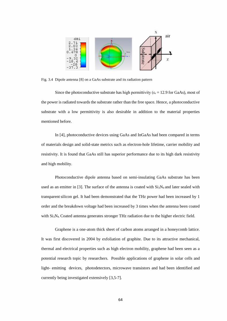
64
Fig. 3.4 Dipole antenna [8] on a GaAs substrate and its radiation pattern
Since the photoconductive substrate has high permittivity (εr = 12.9 for GaAs), most of
the power is radiated towards the substrate rather than the free space. Hence, a photoconductive
substrate with a low permittivity is also desirable in addition to the material properties
mentioned before.
In [4], photoconductive devices using GaAs and InGaAs had been compared in terms
of materials design and solid-state metrics such as electron-hole lifetime, carrier mobility and
resistivity. It is found that GaAs still has superior performance due to its high dark resistivity
and high mobility.
Photoconductive dipole antenna based on semi-insulating GaAs substrate has been
used as an emitter in [3]. The surface of the antenna is coated with Si3N4 and later sealed with
transparent silicon gel. It had been demonstrated that the THz power had been increased by 1
order and the breakdown voltage had been increased by 3 times when the antenna been coated
with Si3N4. Coated antenna generates stronger THz radiation due to the higher electric field.
Graphene is a one-atom thick sheet of carbon atoms arranged in a honeycomb lattice.
It was first discovered in 2004 by exfoliation of graphite. Due to its attractive mechanical,
thermal and electrical properties such as high electron mobility, graphene had been seen as a
potential research topic by researchers. Possible applications of graphene in solar cells and
light- emitting devices, photodetectors, microwave transistors and had been identified and
currently being investigated extensively [3,5-7].
65
Graphene offers a substantial advantage as its properties can be readily tuned by
applying a gate voltage. In [10], a dipole antenna made by gold deposition on a graphene layer
placed on a grown over a SiO2/Si substrate had been studied. It had been shown that by tuning
the gate voltage, the radiation pattern could be exploited. The radiation pattern is switched ON
and OFF by the two states of resistivity in graphene. At 1.05THz by using IE3D software, the
radiation efficiency is 95.80%, and the antenna efficiency is 89.14%.
In [11], a graphene dipole-like antenna had also been studied. However, graphene is
now used as an electrode instead as a substrate. The proposed antenna was simulated using
Ansys HFSS. Values of 0-0.2 eV range of chemical potential had been chosen base on
experimental activity. The gate voltage used is between 0-3 V. By varying the chemical
potential, it had been demonstrated that radiation efficiencies increases.
3.3 Simulation Results
3.3.1 Substrate Thickness
Firstly, the length and the width of the substrate are both fixed to 150 µm, and the
frequencies are varied from 0.5 THz to 1 THz. The substrate thickness, however, is varied from
15 µm to 300 µm. Fig. 3.5 shows that at 1 THz the radiated power is higher once the thickness
of the substrate is at the minimum size which is at 15 µm. Fig. 3.6 shows that at 1 THz, the
efficiency is greater once the thickness of the substrate is at the minimum size which is at 15
µm. The results consist with the findings in [1]. It was found that when increasing the thickness
of the substrate, the dipole antennas couple power to higher-order substrate modes. Also, more
than 90% of the power can be trapped in the substrate. Therefore, not all the power radiated
from the dipole structure can be directly transferred into the air.
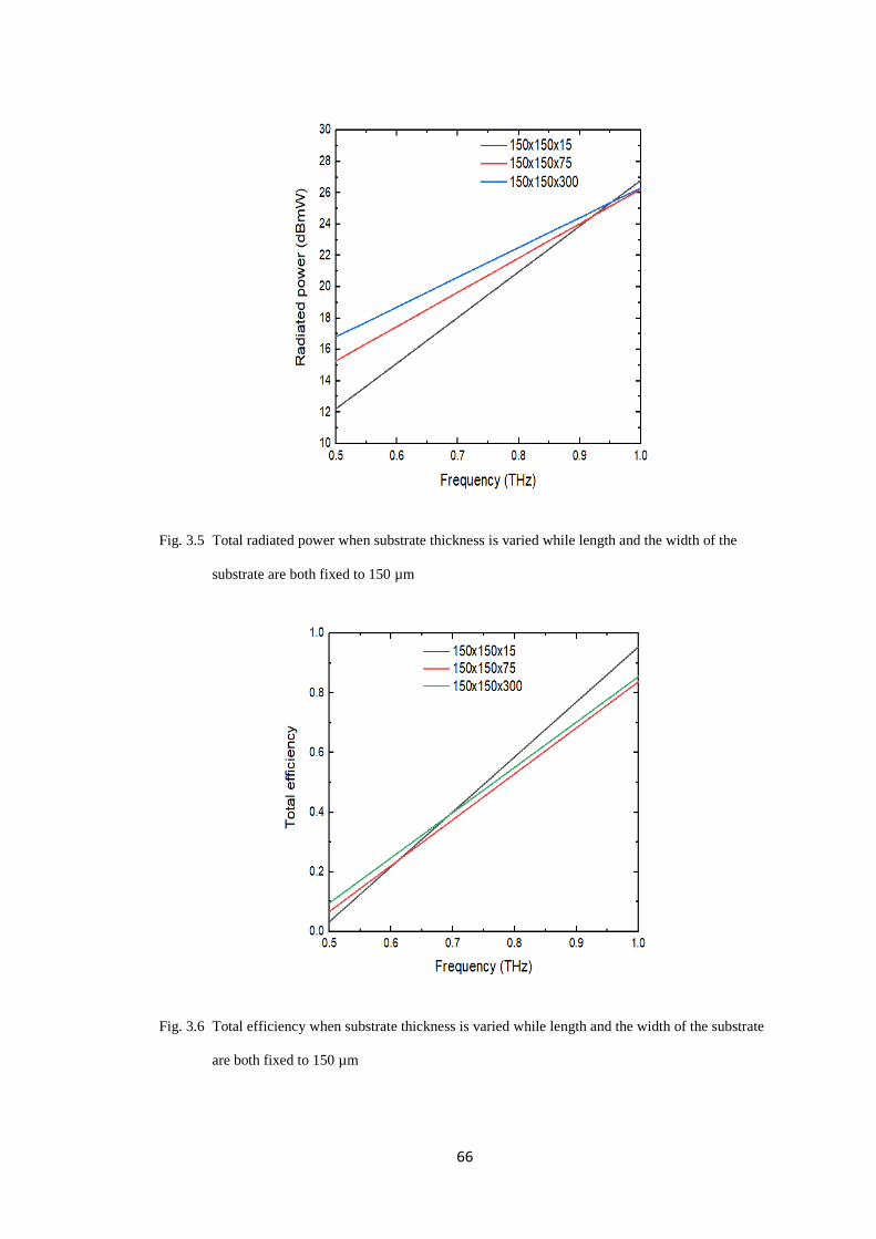
66
Fig. 3.5 Total radiated power when substrate thickness is varied while length and the width of the
substrate are both fixed to 150 µm
Fig. 3.6 Total efficiency when substrate thickness is varied while length and the width of the substrate
are both fixed to 150 µm
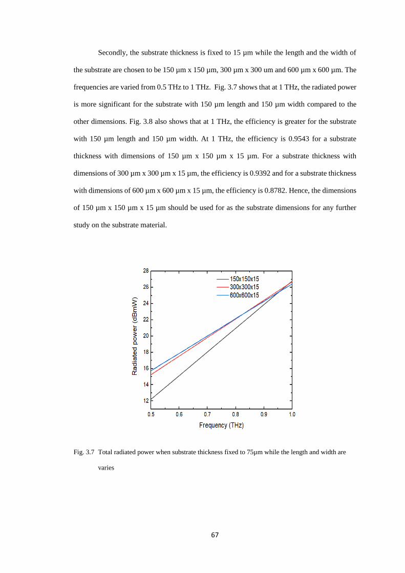
67
Secondly, the substrate thickness is fixed to 15 µm while the length and the width of
the substrate are chosen to be 150 µm x 150 µm, 300 µm x 300 um and 600 µm x 600 µm. The
frequencies are varied from 0.5 THz to 1 THz. Fig. 3.7 shows that at 1 THz, the radiated power
is more significant for the substrate with 150 µm length and 150 µm width compared to the
other dimensions. Fig. 3.8 also shows that at 1 THz, the efficiency is greater for the substrate
with 150 µm length and 150 µm width. At 1 THz, the efficiency is 0.9543 for a substrate
thickness with dimensions of 150 µm x 150 µm x 15 µm. For a substrate thickness with
dimensions of 300 µm x 300 µm x 15 µm, the efficiency is 0.9392 and for a substrate thickness
with dimensions of 600 µm x 600 µm x 15 µm, the efficiency is 0.8782. Hence, the dimensions
of 150 µm x 150 µm x 15 µm should be used for as the substrate dimensions for any further
study on the substrate material.
Fig. 3.7 Total radiated power when substrate thickness fixed to 75µm while the length and width are
varies
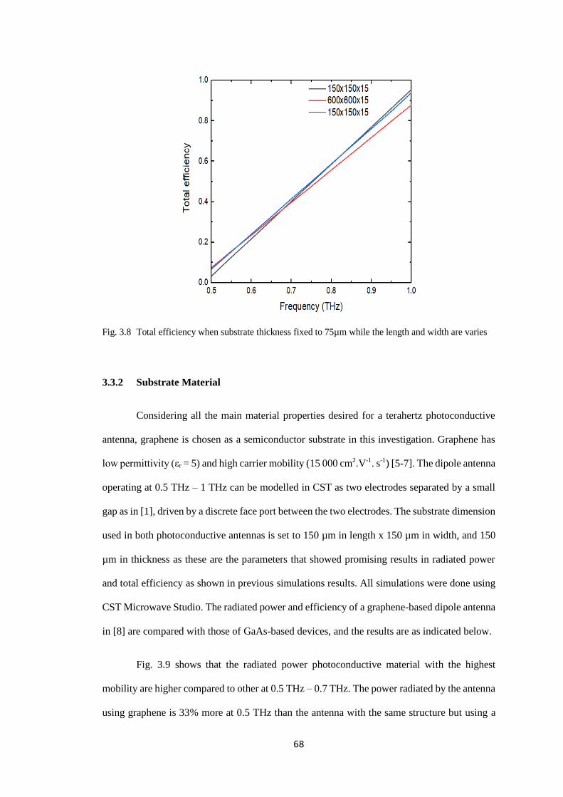
68
Fig. 3.8 Total efficiency when substrate thickness fixed to 75µm while the length and width are varies
3.3.2 Substrate Material
Considering all the main material properties desired for a terahertz photoconductive
antenna, graphene is chosen as a semiconductor substrate in this investigation. Graphene has
low permittivity (εr = 5) and high carrier mobility (15 000 cm2.V-1. s-1) [5-7]. The dipole antenna
operating at 0.5 THz – 1 THz can be modelled in CST as two electrodes separated by a small
gap as in [1], driven by a discrete face port between the two electrodes. The substrate dimension
used in both photoconductive antennas is set to 150 µm in length x 150 µm in width, and 150
µm in thickness as these are the parameters that showed promising results in radiated power
and total efficiency as shown in previous simulations results. All simulations were done using
CST Microwave Studio. The radiated power and efficiency of a graphene-based dipole antenna
in [8] are compared with those of GaAs-based devices, and the results are as indicated below.
Fig. 3.9 shows that the radiated power photoconductive material with the highest
mobility are higher compared to other at 0.5 THz – 0.7 THz. The power radiated by the antenna
using graphene is 33% more at 0.5 THz than the antenna with the same structure but using a
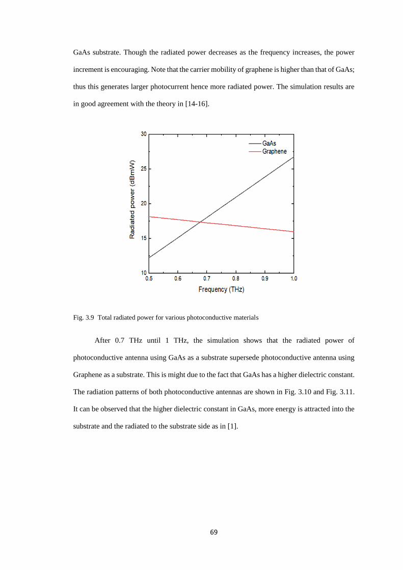
69
GaAs substrate. Though the radiated power decreases as the frequency increases, the power
increment is encouraging. Note that the carrier mobility of graphene is higher than that of GaAs;
thus this generates larger photocurrent hence more radiated power. The simulation results are
in good agreement with the theory in [14-16].
Fig. 3.9 Total radiated power for various photoconductive materials
After 0.7 THz until 1 THz, the simulation shows that the radiated power of
photoconductive antenna using GaAs as a substrate supersede photoconductive antenna using
Graphene as a substrate. This is might due to the fact that GaAs has a higher dielectric constant.
The radiation patterns of both photoconductive antennas are shown in Fig. 3.10 and Fig. 3.11.
It can be observed that the higher dielectric constant in GaAs, more energy is attracted into the
substrate and the radiated to the substrate side as in [1].
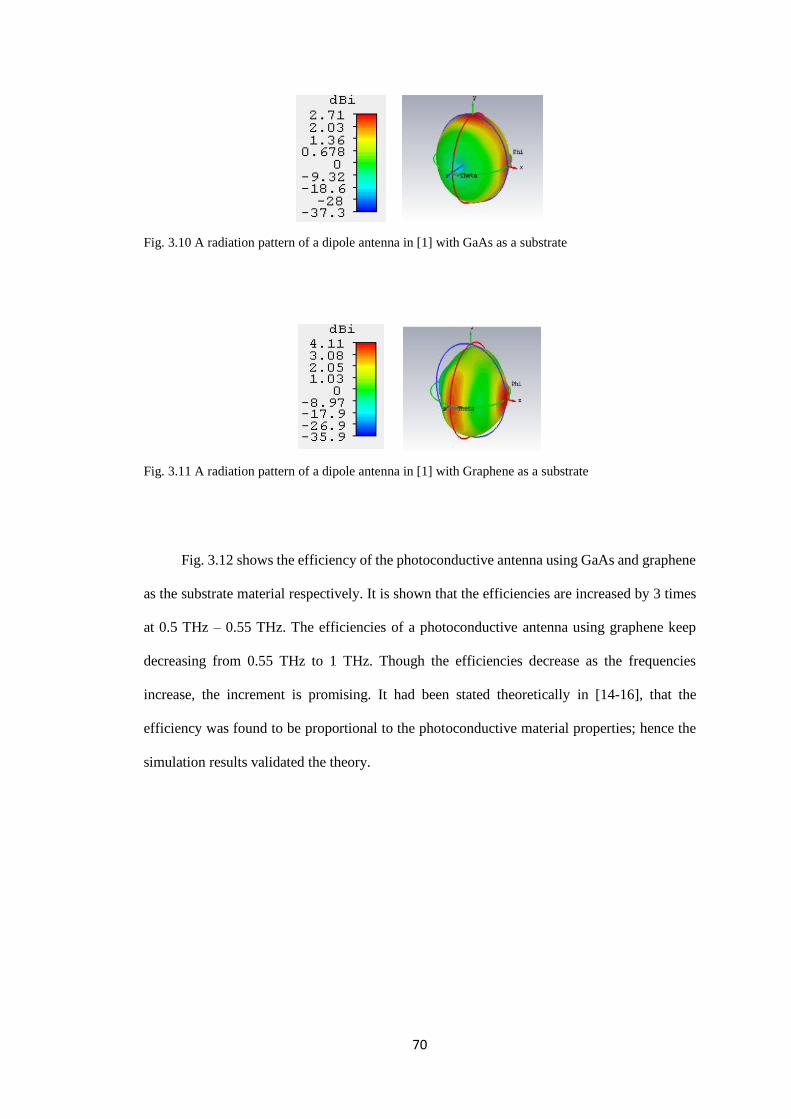
70
Fig. 3.10 A radiation pattern of a dipole antenna in [1] with GaAs as a substrate
Fig. 3.11 A radiation pattern of a dipole antenna in [1] with Graphene as a substrate
Fig. 3.12 shows the efficiency of the photoconductive antenna using GaAs and graphene
as the substrate material respectively. It is shown that the efficiencies are increased by 3 times
at 0.5 THz – 0.55 THz. The efficiencies of a photoconductive antenna using graphene keep
decreasing from 0.55 THz to 1 THz. Though the efficiencies decrease as the frequencies
increase, the increment is promising. It had been stated theoretically in [14-16], that the
efficiency was found to be proportional to the photoconductive material properties; hence the
simulation results validated the theory.
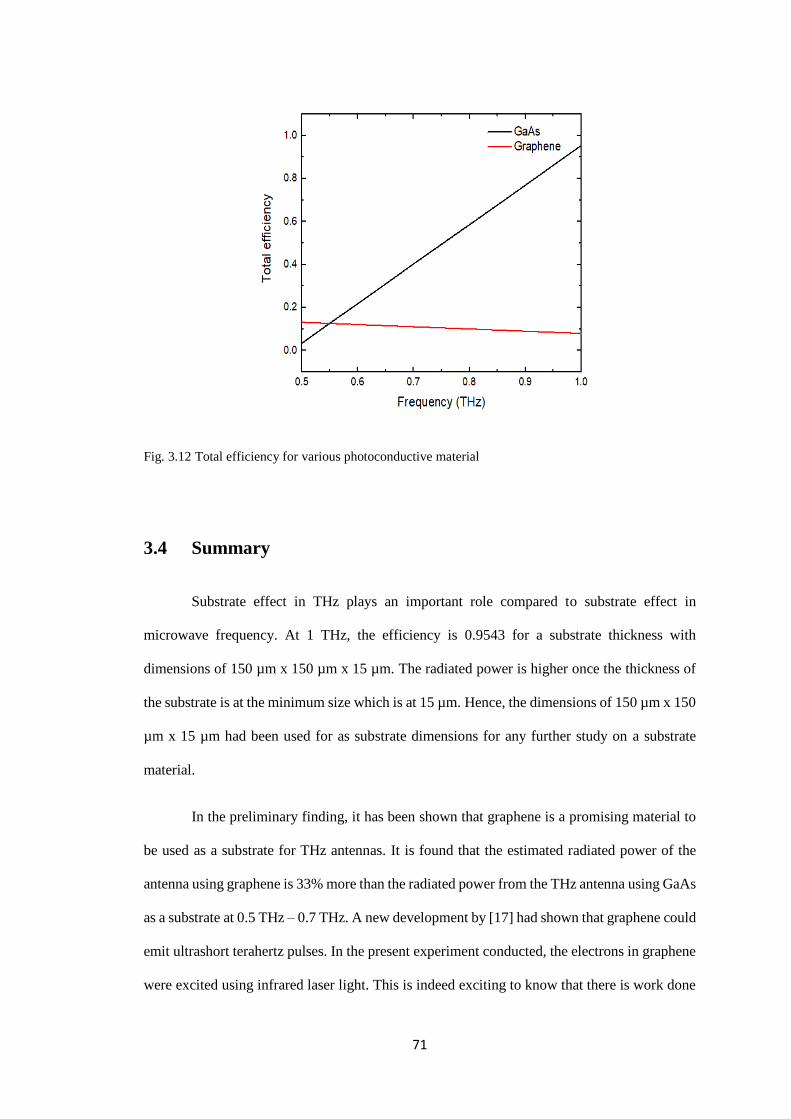
71
Fig. 3.12 Total efficiency for various photoconductive material
3.4 Summary
Substrate effect in THz plays an important role compared to substrate effect in
microwave frequency. At 1 THz, the efficiency is 0.9543 for a substrate thickness with
dimensions of 150 µm x 150 µm x 15 µm. The radiated power is higher once the thickness of
the substrate is at the minimum size which is at 15 µm. Hence, the dimensions of 150 µm x 150
µm x 15 µm had been used for as substrate dimensions for any further study on a substrate
material.
In the preliminary finding, it has been shown that graphene is a promising material to
be used as a substrate for THz antennas. It is found that the estimated radiated power of the
antenna using graphene is 33% more than the radiated power from the THz antenna using GaAs
as a substrate at 0.5 THz – 0.7 THz. A new development by [17] had shown that graphene could
emit ultrashort terahertz pulses. In the present experiment conducted, the electrons in graphene
were excited using infrared laser light. This is indeed exciting to know that there is work done

72
experimentally to show that graphene can emit laser terahertz radiation. This finding, however,
can be more elaborated in details.
Due to the limitations of the CST Microwave Studio software wherein the student
edition, only 30 000 mesh cells can be simulated; another potential software needs to be
reconsidered to prove the theory discussed more accurately. This limitation also only allows a
narrow frequency range. New potential simulation software such as Comsol will provide more
accurate results on the effects of a substrate material of a photoconductive antenna.
73
References
[1] D. Li, Y. Huang, Y. Shen, and N. Khiabani, “Effects of substrate on the performance
of photoconductive THz antennas”, Proceeding of the iWAT 2010, 2010.
[2] B. Ferguson, and X. Zhang, “Materials for Terahertz science and technology”, Nature
Materials, vol. 1, p. 26-33, 2002.
[3] J. Xu, W. Shi, L. Hou, W. Jia, K. Liu, X. Xei, and X. C. Zhang “Terahertz generation
from multiple transparent dielectric coated GaAs antenna”, 12th International
Conference on Terahertz Electronics, 2004.
[4] M. Martin, and E. R. Brown, “Critical Comparison of GaAs and InGaAs THz
Photoconductor”, Conference 8261, SPIE Photonics West, San Franscico, January 21-
26, 2012.
[5] T. Palacios, A. Hsu, and H. Wang, “Applications of graphene devices in RF
communications”, Communications Magazine, IEEE 48.6, p. 122-128, 2010.
[6] A. K. Geim, and K. S. Novoselov, “The rise of graphene”, Nat Matter, vol. 6, p.183-
191, 2007.
[7] P. Tassin, T. Koschny, and C. M. Soukoulis, “Graphene for Terahertz applications”,
Science, vol. 341, p. 620-621, 2013.
[8] D. R. Jackson, and N. G. Alexopolous, “Microstrip dipoles on electrically thick
substrates,” International Journal of Infrared and Millimetre Waves, vol.7, No 1,
1986.
[9] N. G. Alexopoulos, P. B. Katehi, and D. B. Rutledge, “Substrate optimisation for
integrated circuit antennas”, IEEE Transactions on Microwave Theory and
Techniques, vol 31, No 7, July 1983.
74
[10] M. Dragoman, A. A. Muller, D. Dragoman, F. Coccetti, and R. Plana, “Terahertz
antenna based on graphene”, Journal of Applied Physics, p. 107-109, 2010.
[11] M. Tamagnone, J. S. Gomez Diaz, J. R. Mosig and J. Perruisseau-Carrier, “Analysis
and design of terahertz antennas based on plasmonic resonant graphene sheets”,
Journal of Applied Physics, p.112, 2012.
[12] J. S. Gomez-.Diaz and J. Perruisseau-Carrier “Microwave to THz properties of
graphene and potential antenna applications”, Proceeding of ISAP2012, pp.239-242,
2012.
[13] J. Perruisseau-Carrier “Graphene for antenna applications: Opportunities and
challenges from microwave to THz”, Loughborough Antennas & Propagation
Conference, 2012.
[14] N. Khiabani, Y. Huang, Y. Shen, “Discussions on the main parameters of THz
photoconductive antenna as emitters”, Proceeding of the 5th EuCAP, pp.462-466,
April 2011.
[15] Y. Huang, N. Khiabani, Y. Shen and D. Li, “A Further Study of THz Photoconductive
Antennas”, Antennas and Propagation Society International Symposium (APSURSI),
2012.
[16] N. Khiabani, Y. Huang, Y. Shen, L. E. Garcia-Munoz, A. Rivera-Lavado, “A Novel
THz Photomixer Antenna with Trapezoidal Electrodes”, submitted to IEEE
Transactions on Terahertz Science and Technology, 2013.
[17] I. Gierz, J. C. Petersen, M. Mitrano, C. Cacho. E. Turcu, E. Springate, A. Stohr, A.
Kohler, U. Starke and A. Cavelleri, “Non-equilibrium Dirac carrier distributions in
graphene”, Nature Materials, 2013.
[18] Y. Lee, Principles of terahertz science and technology, 1st ed. New York, NY:
Springer, 2008.
75
Chapter 4 The Effect of Electrode Design on THz
Photoconductive Antenna
4.1 Introduction
A comprehensive literature survey [1-3] had summarised the main parameters that
can be the solution in producing high THz output power and high optical-to-THz efficiency
from the antenna. Studies had been done on the sizes of the antenna gap where sharp tip ends
will produce high photo- carrier acceleration. Types of laser excitation also had been studied.
The findings had been summarised in Fig. 4.1.
Nevertheless, none of the parameter studied below had been focusing on the electrode
structure and electrode material that may lead to higher THz power. This chapter will focus
solely on the effect of the electrode structure to the THz radiated power. This chapter also
will focus on the impact of electrode material to the THz radiated power. Comparing a dipole
antenna with an electrode made from noble materials with graphene and nitrides, a
metamaterial will provide insight on the best electrode material for THz photoconductive
antenna.

76
Fig. 4.1 Contribution of each parameter on THz output power and optical-to THz conversion
efficiency [1-3]
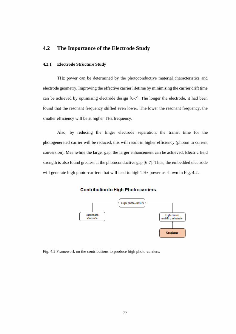
77
4.2 The Importance of the Electrode Study
4.2.1 Electrode Structure Study
THz power can be determined by the photoconductive material characteristics and
electrode geometry. Improving the effective carrier lifetime by minimising the carrier drift time
can be achieved by optimising electrode design [6-7]. The longer the electrode, it had been
found that the resonant frequency shifted even lower. The lower the resonant frequency, the
smaller efficiency will be at higher THz frequency.
Also, by reducing the finger electrode separation, the transit time for the
photogenerated carrier will be reduced, this will result in higher efficiency (photon to current
conversion). Meanwhile the larger gap, the larger enhancement can be achieved. Electric field
strength is also found greatest at the photoconductive gap [6-7]. Thus, the embedded electrode
will generate high photo-carriers that will lead to high THz power as shown in Fig. 4.2.
Fig. 4.2 Framework on the contributions to produce high photo-carriers.
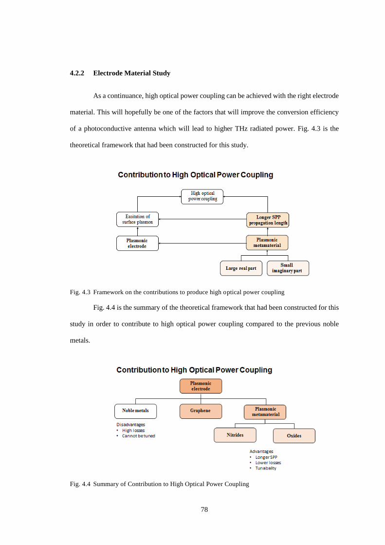
78
4.2.2 Electrode Material Study
As a continuance, high optical power coupling can be achieved with the right electrode
material. This will hopefully be one of the factors that will improve the conversion efficiency
of a photoconductive antenna which will lead to higher THz radiated power. Fig. 4.3 is the
theoretical framework that had been constructed for this study.
Fig. 4.3 Framework on the contributions to produce high optical power coupling
Fig. 4.4 is the summary of the theoretical framework that had been constructed for this
study in order to contribute to high optical power coupling compared to the previous noble
metals.
Fig. 4.4 Summary of Contribution to High Optical Power Coupling
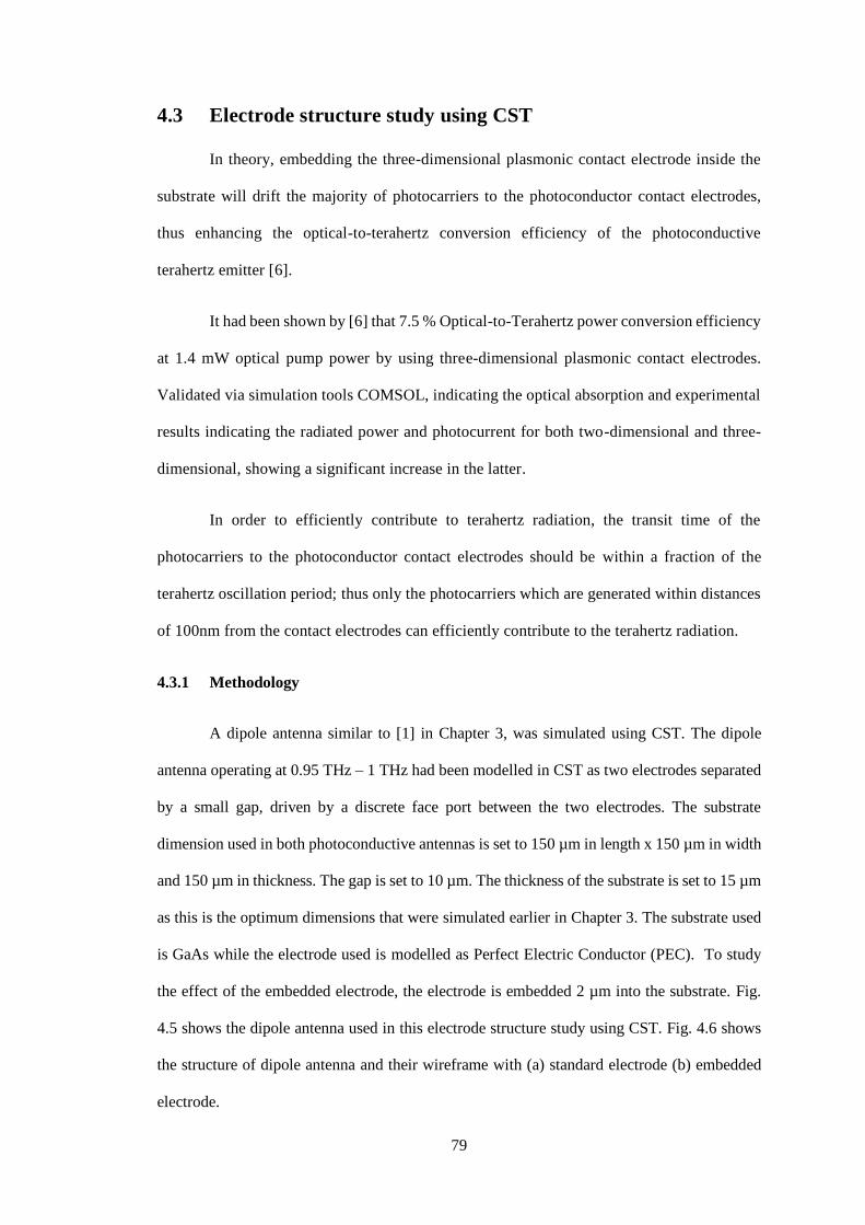
79
4.3 Electrode structure study using CST
In theory, embedding the three-dimensional plasmonic contact electrode inside the
substrate will drift the majority of photocarriers to the photoconductor contact electrodes,
thus enhancing the optical-to-terahertz conversion efficiency of the photoconductive
terahertz emitter [6].
It had been shown by [6] that 7.5 % Optical-to-Terahertz power conversion efficiency
at 1.4 mW optical pump power by using three-dimensional plasmonic contact electrodes.
Validated via simulation tools COMSOL, indicating the optical absorption and experimental
results indicating the radiated power and photocurrent for both two-dimensional and three-
dimensional, showing a significant increase in the latter.
In order to efficiently contribute to terahertz radiation, the transit time of the
photocarriers to the photoconductor contact electrodes should be within a fraction of the
terahertz oscillation period; thus only the photocarriers which are generated within distances
of 100nm from the contact electrodes can efficiently contribute to the terahertz radiation.
4.3.1 Methodology
A dipole antenna similar to [1] in Chapter 3, was simulated using CST. The dipole
antenna operating at 0.95 THz – 1 THz had been modelled in CST as two electrodes separated
by a small gap, driven by a discrete face port between the two electrodes. The substrate
dimension used in both photoconductive antennas is set to 150 µm in length x 150 µm in width
and 150 µm in thickness. The gap is set to 10 µm. The thickness of the substrate is set to 15 µm
as this is the optimum dimensions that were simulated earlier in Chapter 3. The substrate used
is GaAs while the electrode used is modelled as Perfect Electric Conductor (PEC). To study
the effect of the embedded electrode, the electrode is embedded 2 µm into the substrate. Fig.
4.5 shows the dipole antenna used in this electrode structure study using CST. Fig. 4.6 shows
the structure of dipole antenna and their wireframe with (a) standard electrode (b) embedded
electrode.
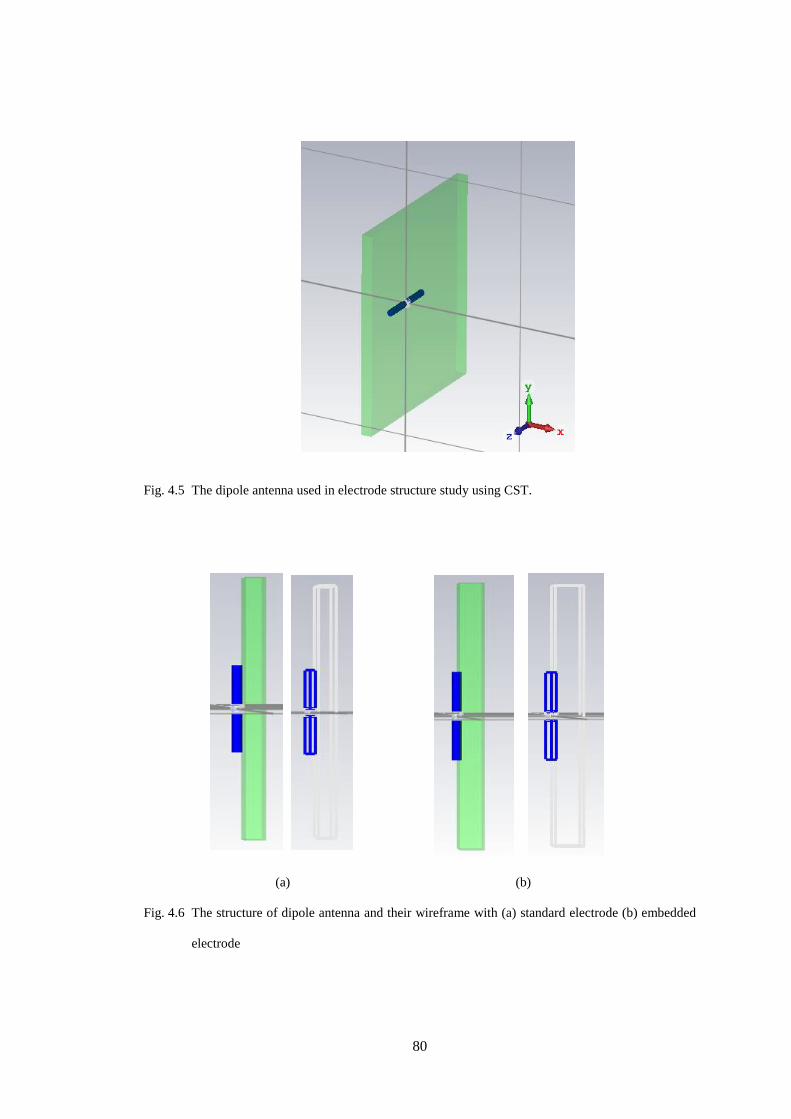
80
Fig. 4.5 The dipole antenna used in electrode structure study using CST.
(a) (b)
Fig. 4.6 The structure of dipole antenna and their wireframe with (a) standard electrode (b) embedded
electrode
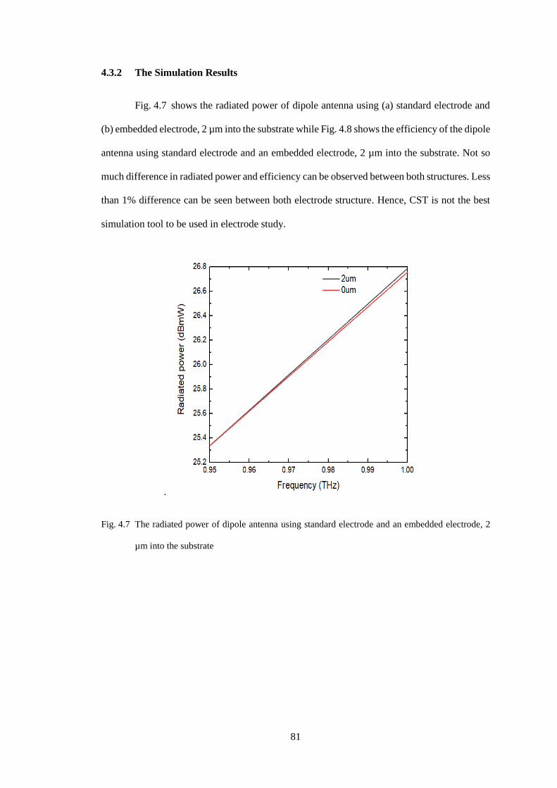
81
4.3.2 The Simulation Results
Fig. 4.7 shows the radiated power of dipole antenna using (a) standard electrode and
(b) embedded electrode, 2 µm into the substrate while Fig. 4.8 shows the efficiency of the dipole
antenna using standard electrode and an embedded electrode, 2 µm into the substrate. Not so
much difference in radiated power and efficiency can be observed between both structures. Less
than 1% difference can be seen between both electrode structure. Hence, CST is not the best
simulation tool to be used in electrode study.
.
Fig. 4.7 The radiated power of dipole antenna using standard electrode and an embedded electrode, 2
µm into the substrate
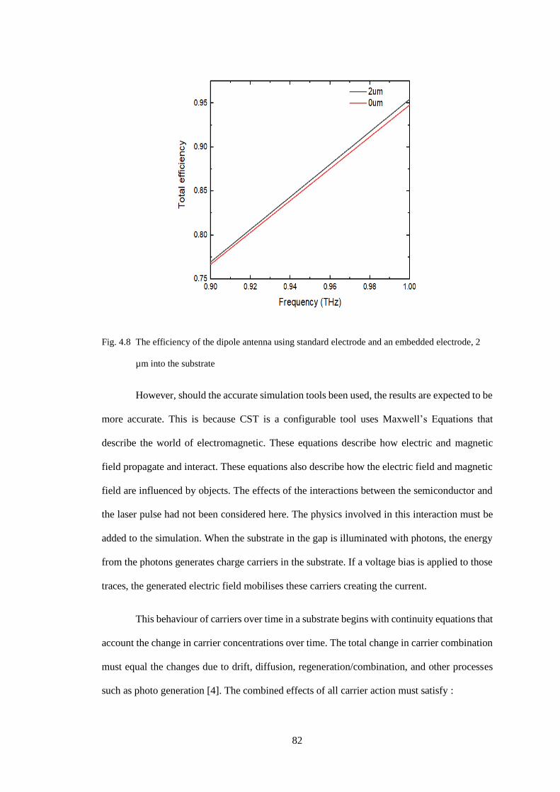
82
Fig. 4.8 The efficiency of the dipole antenna using standard electrode and an embedded electrode, 2
µm into the substrate
However, should the accurate simulation tools been used, the results are expected to be
more accurate. This is because CST is a configurable tool uses Maxwell’s Equations that
describe the world of electromagnetic. These equations describe how electric and magnetic
field propagate and interact. These equations also describe how the electric field and magnetic
field are influenced by objects. The effects of the interactions between the semiconductor and
the laser pulse had not been considered here. The physics involved in this interaction must be
added to the simulation. When the substrate in the gap is illuminated with photons, the energy
from the photons generates charge carriers in the substrate. If a voltage bias is applied to those
traces, the generated electric field mobilises these carriers creating the current.
This behaviour of carriers over time in a substrate begins with continuity equations that
account the change in carrier concentrations over time. The total change in carrier combination
must equal the changes due to drift, diffusion, regeneration/combination, and other processes
such as photo generation [4]. The combined effects of all carrier action must satisfy :
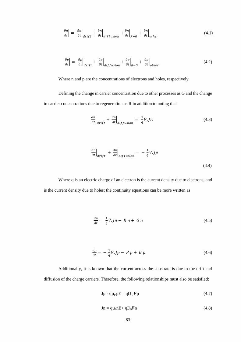
83
𝜕𝑛
𝜕𝑡| =
𝜕𝑛
𝜕𝑡|
𝑑𝑟𝑖𝑓𝑡+
𝜕𝑛
𝜕𝑡|
𝑑𝑖𝑓𝑓𝑢𝑠𝑖𝑜𝑛+
𝜕𝑛
𝜕𝑡|
𝑅−𝐺+
𝜕𝑛
𝜕𝑡|
𝑜𝑡ℎ𝑒𝑟 (4.1)
𝜕𝑝
𝜕𝑡| =
𝜕𝑝
𝜕𝑡|
𝑑𝑟𝑖𝑓𝑡+
𝜕𝑝
𝜕𝑡|
𝑑𝑖𝑓𝑓𝑢𝑠𝑖𝑜𝑛+
𝜕𝑝
𝜕𝑡|
𝑅−𝐺+
𝜕𝑝
𝜕𝑡|
𝑜𝑡ℎ𝑒𝑟 (4.2)
Where n and p are the concentrations of electrons and holes, respectively.
Defining the change in carrier concentration due to other processes as G and the change
in carrier concentrations due to regeneration as R in addition to noting that
𝜕𝑛
𝜕𝑡|
𝑑𝑟𝑖𝑓𝑡+
𝜕𝑛
𝜕𝑡|
𝑑𝑖𝑓𝑓𝑢𝑠𝑖𝑜𝑛=
1
𝑞𝛻. 𝐽𝑛 (4.3)
𝜕𝑛
𝜕𝑡|
𝑑𝑟𝑖𝑓𝑡 +
𝜕𝑛
𝜕𝑡|
𝑑𝑖𝑓𝑓𝑢𝑠𝑖𝑜𝑛= −
1
𝑞𝛻. 𝐽𝑝
(4.4)
Where q is an electric charge of an electron is the current density due to electrons, and
is the current density due to holes; the continuity equations can be more written as
𝜕𝑛
𝜕𝑡 =
1
𝑞𝛻. 𝐽𝑛 − 𝑅 𝑛 + 𝐺 𝑛 (4.5)
𝜕𝑝
𝜕𝑡 = −
1
𝑞𝛻. 𝐽𝑝 − 𝑅 𝑝 + 𝐺 𝑝 (4.6)
Additionally, it is known that the current across the substrate is due to the drift and
diffusion of the charge carriers. Therefore, the following relationships must also be satisfied:
Jp ꞊ qµp pE – qD p 𝛻p (4.7)
Jn = qµnnE+ qDn𝛻n (4.8)
84
Where µ and µ are the carrier mobility of the electrons and holes respectively, E is the
electric field, and Dn and Dp are the carrier diffusion coefficients for the electrons and holes
respectively. It is also known that the current density in steady-state conditions [21].
J = Jn +Jp (4.9)
This semiconductor physics equation should be combined with Maxwell’s equations in
order to obtain the accurate results of the expected radiated power of the THz photoconductive
antenna. Thus, the next step is to find out how these properties can be combined together by
using suitable software to produce more accurate results since there is no available software
that is available to do this.
4.4 Electrode material study using CST
4.4.1 The Advantages of Plasmonic Metamaterial
4.4.1.1 Surface Plasmon Excitation
The idea to excite surface plasmon waves had been introduced in [5, 8]. Excitation of
surface plasmon waves allows transmission of the optical pump through the nano fingers made
from gold (aurum) into the photo absorbing substrate. A surface plasmon is a travelling wave
oscillation of electrons that can be excited in the surface of certain metals with the right material
properties. To date, the only noble metals that can exhibit plasmonic characteristics are gold
(aurum) or silver (argentum).
In [5, 8], this paper stated that in the case of the plasmonic photoconductor, the optical
pump is transmitted through the nanoscale metallic grating through the coupling with surface
plasmon. It is also stated that the highest optical absorption and photocarrier generation occurs
in direct proximity to the metal contacts since the excited surface plasmon waves exist at the
dielectric-metal interface. This is what plasmonic metamaterial is made of.
However, as a surface plasmon propagates along the surface, it loses energy to the
metal due to absorption. Hence larger surface plasmon propagation is desirable to ensure that
the excited surface plasmon does not lose its energy/power/intensity too early.
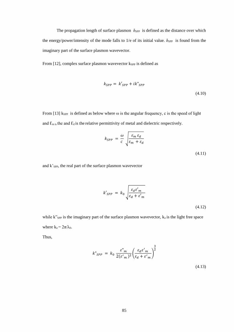
85
The propagation length of surface plasmon δSPP is defined as the distance over which
the energy/power/intensity of the mode falls to 1/e of its initial value. δSPP is found from the
imaginary part of the surface plasmon wavevector.
From [12], complex surface plasmon wavevector kSPP is defined as
𝑘𝑆𝑃𝑃 = 𝑘′𝑆𝑃𝑃 + 𝑖𝑘"𝑆𝑃𝑃
(4.10)
From [13] kSPP is defined as below where ω is the angular frequency, c is the speed of light
and Ɛm is the and Ɛd is the relative permittivity of metal and dielectric respectively.
𝑘𝑆𝑃𝑃 = 𝜔
𝑐 √
휀𝑚 휀𝑑
휀𝑚 + 휀𝑑
(4.11)
and k’SPP, the real part of the surface plasmon wavevector
𝑘′𝑆𝑃𝑃 = 𝑘0 √휀𝑑휀′𝑚
휀𝑑 + 휀′𝑚
(4.12)
while k”SPP is the imaginary part of the surface plasmon wavevector, ko is the light free space
where ko = 2π/λ0.
Thus,
𝑘"𝑆𝑃𝑃 = 𝑘0 휀"𝑚
2(휀′𝑚 )
2 (휀𝑑휀′
𝑚
휀𝑑 + 휀′𝑚
)
32
(4.13)
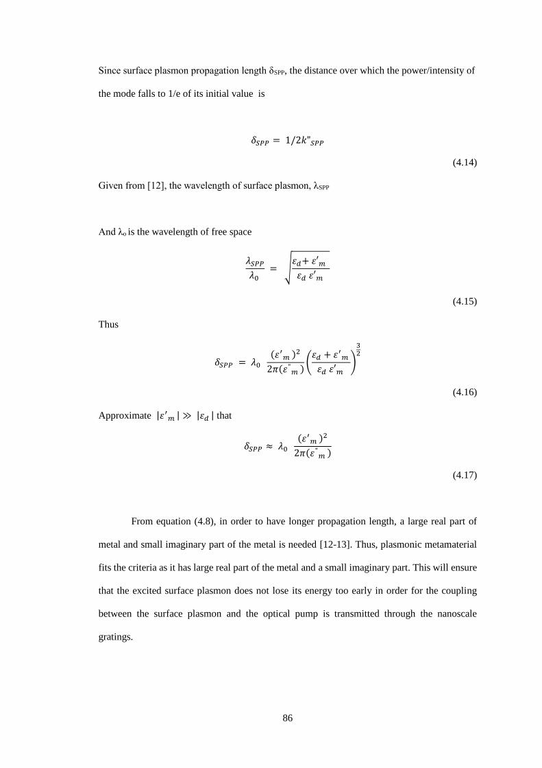
86
Since surface plasmon propagation length δSPP, the distance over which the power/intensity of
the mode falls to 1/e of its initial value is
𝛿𝑆𝑃𝑃 = 1/2𝑘"𝑆𝑃𝑃
(4.14)
Given from [12], the wavelength of surface plasmon, λSPP
And λo is the wavelength of free space
𝜆𝑆𝑃𝑃
𝜆0 = √
휀𝑑+ 휀′𝑚
휀𝑑 휀′𝑚
(4.15)
Thus
𝛿𝑆𝑃𝑃 = 𝜆0 (휀′
𝑚 )2
2𝜋(휀"𝑚 )
(휀𝑑 + 휀′
𝑚
휀𝑑 휀′𝑚 )
32
(4.16)
Approximate |휀′𝑚 | ≫ |휀𝑑 | that
𝛿𝑆𝑃𝑃 ≈ 𝜆0 (휀′
𝑚 )2
2𝜋(휀"𝑚 )
(4.17)
From equation (4.8), in order to have longer propagation length, a large real part of
metal and small imaginary part of the metal is needed [12-13]. Thus, plasmonic metamaterial
fits the criteria as it has large real part of the metal and a small imaginary part. This will ensure
that the excited surface plasmon does not lose its energy too early in order for the coupling
between the surface plasmon and the optical pump is transmitted through the nanoscale
gratings.
87
A comparison is made on the dielectric function of Titanium Nitride (TiN), in contrast
with conventional plasmonic materials in [14-15] as shown in Fig. 4.9 proves that the real part
of these highly potential plasmonic metamaterials is more significant.
Fig. 4.9 Comparison done on the dielectric function of plasmonic metamaterial TiN with conventional
metals [14-15]
The imaginary part of Titanium Nitride (TiN), is comparable to the conventional
metals. Thus this proves that plasmonic metamaterial is an excellent candidate to replace
conventional metals such as Gold (Aurum) or Silver (Argentum).
4.4.1.2 High Loss of Noble Metals
In [9,16], noble metals had been shown to have substantial carrier concentrations,
which in turns makes their plasma frequencies very large [14]. A large plasma frequency
produces a large imaginary permittivity which translates to a significant loss. Plasmonic
metamaterial, however, has lower carrier concentrations hence smaller losses.
Experimentally, losses result in [9,16] of the alternatives plasmonic metamaterials of
oxides and nitrides compared to Gold (Aurum) or Silver (Argentum) shown that the imaginary
part of the plasmonic metamaterial of oxides (transparent conducting oxides) are found smaller
compared to the noble metals.
88
4.4.2 Methodology
Again, a dipole antenna similar to [1] was simulated using CST. The dipole antenna
operating at 0.95 THz – 1 THz had been modelled in CST as two electrodes separated by a
small gap, driven by a discrete face port between the two electrodes. The substrate dimension
used in both photoconductive antennas is set to 150 µm in length x 150 µm in width and 150
µm in thickness. The gap is set to 10 µm. The thickness of the substrate is also set to 15 µm as
this is the optimum dimensions that were simulated earlier in Chapter 3. The substrate used is
GaAs while the electrodes material used are graphene, Gold (Aurum), Silver (Argentum) and
Titanium Nitride (TiN). Defined in CST’s material library, Gold has an electric conductivity of
6.3012 x 10⁷ S/m, while Silver has an electric conductivity of 4.561 x 10⁷ S/m. These
simulations were repeated for three times, and the result is shown in Fig. 4.10.
4.4.2.2 The Simulation Results
Fig. 4.10 shows the radiated power of the dipole antenna using an electrode made from
noble metals and metamaterial. As expected, graphene performed better than gold and silver
due to its material properties such as higher carrier mobility. Titanium nitride (TiN), performed
second after Graphene. This confirms the experimental results in [10-11] that the noble metal
losses found to be higher compared to metamaterial. These simulation results agree with the
experimental done in [10-11]. Thus, this finding will be beneficial for design purposes. The
radiation patterns of these simulations are shown in Fig. 4.11 for the graphene electrode, Fig.
4.12 for the gold electrode, Fig. 4.12 for the silver electrode and Fig. 4.13 for the TiN electrode.
The radiation pattern of an electrode using noble metals becomes asymmetrical. This radiation
pattern enhanced towards the substrate. Hence, this might explain the lower radiated power
using noble metals as the power can be trapped in the substrate.
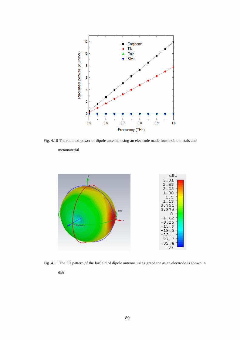
89
Fig. 4.10 The radiated power of dipole antenna using an electrode made from noble metals and
metamaterial
Fig. 4.11 The 3D pattern of the farfield of dipole antenna using graphene as an electrode is shown in
dBi
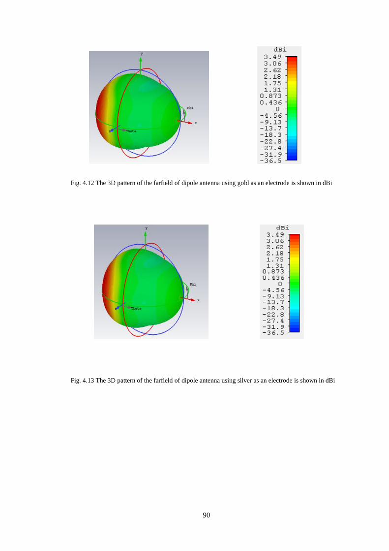
90
Fig. 4.12 The 3D pattern of the farfield of dipole antenna using gold as an electrode is shown in dBi
Fig. 4.13 The 3D pattern of the farfield of dipole antenna using silver as an electrode is shown in dBi
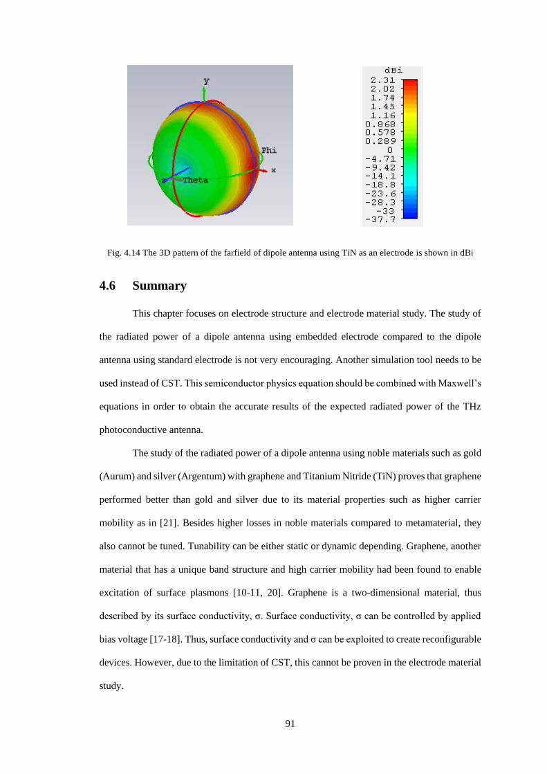
91
Fig. 4.14 The 3D pattern of the farfield of dipole antenna using TiN as an electrode is shown in dBi
4.6 Summary
This chapter focuses on electrode structure and electrode material study. The study of
the radiated power of a dipole antenna using embedded electrode compared to the dipole
antenna using standard electrode is not very encouraging. Another simulation tool needs to be
used instead of CST. This semiconductor physics equation should be combined with Maxwell’s
equations in order to obtain the accurate results of the expected radiated power of the THz
photoconductive antenna.
The study of the radiated power of a dipole antenna using noble materials such as gold
(Aurum) and silver (Argentum) with graphene and Titanium Nitride (TiN) proves that graphene
performed better than gold and silver due to its material properties such as higher carrier
mobility as in [21]. Besides higher losses in noble materials compared to metamaterial, they
also cannot be tuned. Tunability can be either static or dynamic depending. Graphene, another
material that has a unique band structure and high carrier mobility had been found to enable
excitation of surface plasmons [10-11, 20]. Graphene is a two-dimensional material, thus
described by its surface conductivity, σ. Surface conductivity, σ can be controlled by applied
bias voltage [17-18]. Thus, surface conductivity and σ can be exploited to create reconfigurable
devices. However, due to the limitation of CST, this cannot be proven in the electrode material
study.
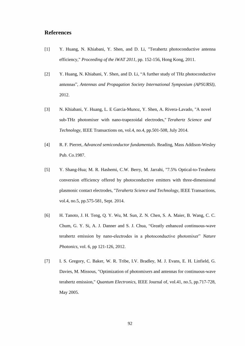
92
References
[1] Y. Huang, N. Khiabani, Y. Shen, and D. Li, "Terahertz photoconductive antenna
efficiency," Proceeding of the iWAT 2011, pp. 152-156, Hong Kong, 2011.
[2] Y. Huang, N. Khiabani, Y. Shen, and D. Li, “A further study of THz photoconductive
antennas”, Antennas and Propagation Society International Symposium (APSURSI),
2012.
[3] N. Khiabani, Y. Huang, L. E Garcia-Munoz, Y. Shen, A. Rivera-Lavado, "A novel
sub-THz photomixer with nano-trapezoidal electrodes," Terahertz Science and
Technology, IEEE Transactions on, vol.4, no.4, pp.501-508, July 2014.
[4] R. F. Pierret, Advanced semiconductor fundamentals. Reading, Mass Addison-Wesley
Pub. Co.1987.
[5] Y. Shang-Hua; M. R. Hashemi, C.W. Berry, M. Jarrahi, "7.5% Optical-to-Terahertz
conversion efficiency offered by photoconductive emitters with three-dimensional
plasmonic contact electrodes, "Terahertz Science and Technology, IEEE Transactions,
vol.4, no.5, pp.575-581, Sept. 2014.
[6] H. Tanoto, J. H. Teng, Q. Y. Wu, M. Sun, Z. N. Chen, S. A. Maier, B. Wang, C. C.
Chum, G. Y. Si, A. J. Danner and S. J. Chua, “Greatly enhanced continuous-wave
terahertz emission by nano-electrodes in a photoconductive photomixer” Nature
Photonics, vol. 6, pp 121-126, 2012.
[7] I. S. Gregory, C. Baker, W. R. Tribe, I.V. Bradley, M. J. Evans, E. H. Linfield, G.
Davies, M. Missous, "Optimization of photomixers and antennas for continuous-wave
terahertz emission," Quantum Electronics, IEEE Journal of, vol.41, no.5, pp.717-728,
May 2005.
93
[8] C. W. Berry, M. R. Hashemi, M. Unlu, and M. Jarrahi, “Significant radiation
enhancement in photoconductive terahertz emitters by incorporating plasmonic
contact electrodes”, Electrical Engineering and Computer Science Department,
University of Michigan Ann Arbor, MI 48109, United States.
[9] A. Boltasseva, H. A. Atwater, “Low-loss plasmonic metamaterials”, School of
Electrical & Computer Engineering and Birck Nanotechnology Center, Purdue
University, Indiana, West Lafayette, IN 47907, USA.
[10] G. V. Naik and A. Boltasseva, “A comparative study of semiconductor-based
plasmonic metamaterials”, Metamaterials 5, vol.1, pp. 1–7, 2011.
[11] P. R. West, S. Ishii, G.V. Naik, N. K. Emani, V. M. Shalaev and A. Boltasseva,
“Searching for better plasmonic materials”, Laser & Photon. Rev., 4: pp.795–808,
2010.
[12] H. Raether, “Surface plasmons on smooth and rough surfaces and on gratings”, 1st
ed., Berlin: Springer, 1998.
[13] W. L. Barnes, “Surface plasmon-polarition length scales: a route to sub-wavelength
optics, J. Opt. A: Pure Appl. Opt. 8 pp.87- 93, 2006
[14] G. V. Naik, J. Kim, and A. Boltasseva, Oxides and nitrides as alternative plasmonic
materials in the optical range, Opt. Mater. Express 1(6),pp.1090-1099, 2011.
[15] G. V. Naik, J. L. Schroeder, N. Xingjie, A. V. Kildishev, T. D. Sands, and A.
Boltasseva, "Titanium nitride as a plasmonic material for visible and near-infrared
wavelengths," Opt. Mater. Express 2, pp.478-489, 2012.
[16] G.V. Naik, J. Kim, and A. Boltasseva, “Plasmonic and metamaterials: looking
beyond gold and silver,” Metamaterials 2012: The Sixth International Congress on
Advanced Electromagnetic Materials in Microwaves and Optics, 2012.
94
[17] M. Dragoman, A. A. Muller, D. Dragoman, F. Coccetti, and R. Plana, “Terahertz
antenna based on graphene”, Journal of Applied Physics, pp. 107-109, 2010.
[18] J. M. Tamagnone, J. S. Gomez Diaz, J. R. Mosig, and J. Perruisseau-Carrier, “Analysis
and design of terahertz antennas based on plasmonic resonant graphene sheets”,
Journal of Applied Physics, pp.112, 2012.
[19] Sigma-Aldrich Corporation, Available: https://www.sigmaaldrich.com/
[20] P. Tassin, T. Koschny, and C. M. Soukoulis, “Graphene for Terahertz applications”,
Science, vol. 341, pp. 620-621, 2013.
[21] A. Abu Bakar Sajak, Y. Shen, Y. Huang, and R. Alrawashdeh, “An investigation on
THz antennas using graphene as a substrate”, The 8th European Conference on
Antennas and Propagation, The Hague, The Netherlands, April, 2014.
95
Chapter 5 Analysis of a Photoconductive Antenna using
COMSOL
5.1 Introduction
Fig. 5.1 and 5.2 show the schematic diagram of the photoconductive antenna structures
and their corresponding dimensions of the conventional and the proposed photoconductive
antenna, respectively. The proposed photoconductive antenna:
Has an embedded electrode in the substrate material
Was fed with both voltage bias and optical pump in the simulation works
Were shown to withstand higher bias voltage than conventional photoconductive
antenna hence higher THz radiation power
For simplicity, LT-GaAs was chosen as the substrate material while Gold was used as
the electrode material in all simulation works. The simulated electric field values were plotted
using the coordinates as defined in Figure 5.2.
Fig. 5.1 The structure of a (a) conventional model photoconductive antenna. (b) proposed model
photoconductive antenna.
(a) (b)
96
Fig. 5.2 Schematic diagram of the structure of a photoconductive antenna (a) conventional model (b)
proposed model and the coordinate of the simulated electric field
A commercial finite-difference time-domain (FDTD) simulation software package
COMSOL version 5.2 was used in all simulation work. Unlike microwave antennas,
photoconductive antennas are fed with two different sources namely the dc voltage bias and the
optical pump. After defining the respective geometries as summarised in Table 5.1, the AC/DC
module in the COMSOL Multiphysics was used to calculate the electric field distribution inside
the photoconductive device when voltage biases were applied to the electrode. The optical
pumps were modelled using the Electromagnetic Waves, Frequency Domain interface in order
to calculate the density distribution of the photo-generated carriers produced by the pump laser.
Table 5.1 Parameters for Comsol Simulation
Parameter Value
Substrate dimension (height x width x depth) 100 μm x 100 μm x 100 μm
Antenna gap 2 μm
Voltage biases 0 V - 4 V
Optical power pumps 1.4 mW - 10 mW
LT-GaAs Relative permittivity (Ɛr) [5-6 ] 12.9
Gold Relative permittivity (Ɛr) [5-6 ] 6.9
Wavelength (λ) 780 nm
Electrode thickness 0.1 μm - 1 μm
(a) (b)
97
5.2 Simulation Method
Using the AC/DC module in COMSOL Multiphysics, the electric field of both the
convention and the proposed antennas is simulated at the wavelength and laser power as shown
in Table 5.1. Fig. 5.3a and b show the electric field map calculated at a voltage bias of 4 V for
a conventional and the proposed antenna, respectively. The electric field is at the strongest at
the sharp edges between the antenna gap. Note that the breakdown electric field of GaAs is 4
x 107 V/m while the breakdown electric field of air is 3 x 10⁶ V/m; hence the chosen voltage
bias of 4 V will not exceed the breakdown electric field of air in the conventional model.
Fig. 5.3 Electric Field of (a) conventional (b) proposed THz photoconductive antenna at
given voltage bias at 4 V
5.3 Simulation Results
5.3.1 Electrode Thickness
Fig. 5.4 shows the electric field distribution along the depth direction in the antenna
substrate. The electric field calculated at the centre of the antenna gap of both the conventional
and proposed photoconductive antenna is plotted against the depth of the substrate, starting
from the substrate surface as indicated in Fig. 5.2. It is found that electrode thickness of the
proposed antenna plays a role; higher electric field over larger depth is observed for a thicker
electrode of the proposed antenna. In contrast, no change of the electric field can be observed
when the electrode thicknesses of the conventional antenna are changed.
(a) (b)
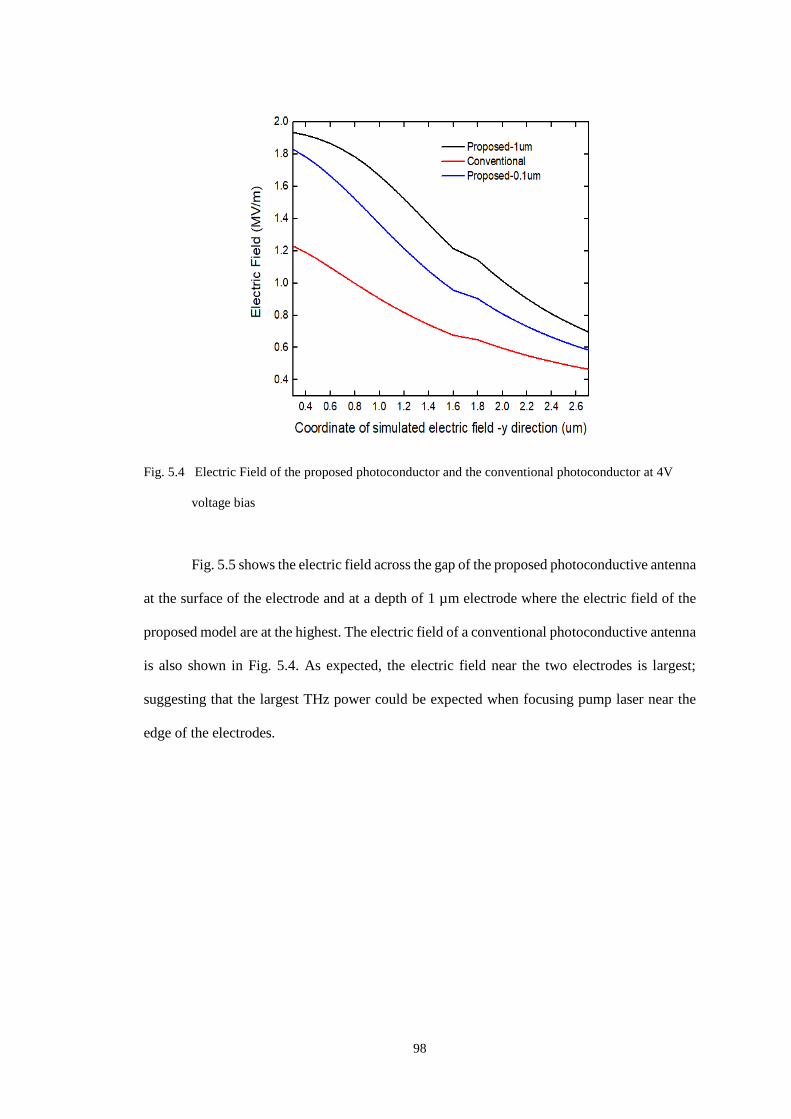
98
Fig. 5.4 Electric Field of the proposed photoconductor and the conventional photoconductor at 4V
voltage bias
Fig. 5.5 shows the electric field across the gap of the proposed photoconductive antenna
at the surface of the electrode and at a depth of 1 µm electrode where the electric field of the
proposed model are at the highest. The electric field of a conventional photoconductive antenna
is also shown in Fig. 5.4. As expected, the electric field near the two electrodes is largest;
suggesting that the largest THz power could be expected when focusing pump laser near the
edge of the electrodes.
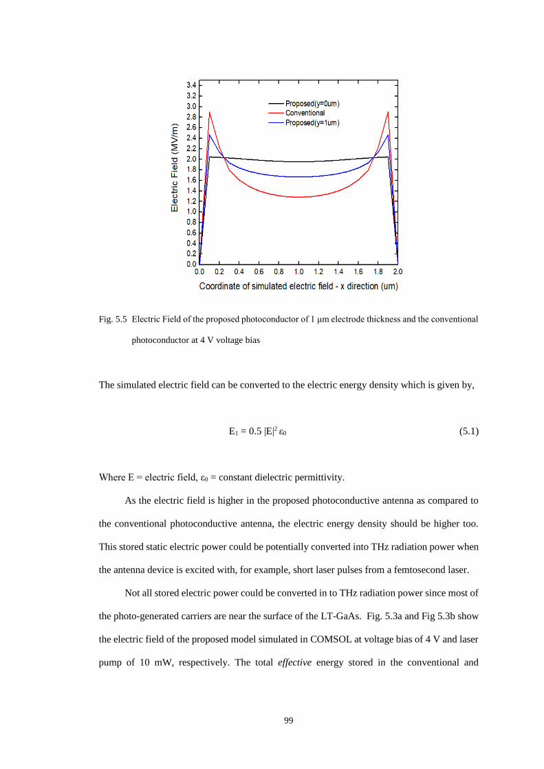
99
Fig. 5.5 Electric Field of the proposed photoconductor of 1 μm electrode thickness and the conventional
photoconductor at 4 V voltage bias
The simulated electric field can be converted to the electric energy density which is given by,
E1 = 0.5 |E|2 ε0 (5.1)
Where E = electric field, ε0 = constant dielectric permittivity.
As the electric field is higher in the proposed photoconductive antenna as compared to
the conventional photoconductive antenna, the electric energy density should be higher too.
This stored static electric power could be potentially converted into THz radiation power when
the antenna device is excited with, for example, short laser pulses from a femtosecond laser.
Not all stored electric power could be converted in to THz radiation power since most of
the photo-generated carriers are near the surface of the LT-GaAs. Fig. 5.3a and Fig 5.3b show
the electric field of the proposed model simulated in COMSOL at voltage bias of 4 V and laser
pump of 10 mW, respectively. The total effective energy stored in the conventional and
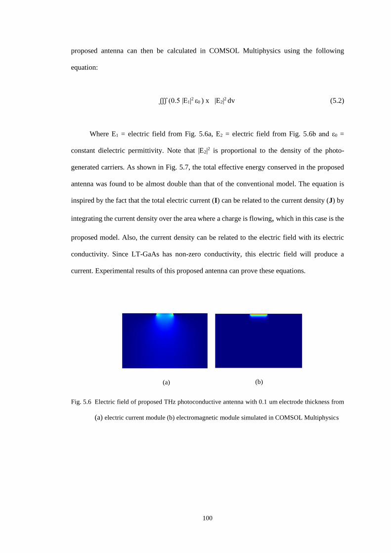
100
proposed antenna can then be calculated in COMSOL Multiphysics using the following
equation:
ʃʃʃ (0.5 |E1|2 ε0 ) x |E2|2 dv (5.2)
Where E1 = electric field from Fig. 5.6a, E2 = electric field from Fig. 5.6b and ε0 =
constant dielectric permittivity. Note that |E2|2 is proportional to the density of the photo-
generated carriers. As shown in Fig. 5.7, the total effective energy conserved in the proposed
antenna was found to be almost double than that of the conventional model. The equation is
inspired by the fact that the total electric current (I) can be related to the current density (J) by
integrating the current density over the area where a charge is flowing, which in this case is the
proposed model. Also, the current density can be related to the electric field with its electric
conductivity. Since LT-GaAs has non-zero conductivity, this electric field will produce a
current. Experimental results of this proposed antenna can prove these equations.
Fig. 5.6 Electric field of proposed THz photoconductive antenna with 0.1 um electrode thickness from
(a) electric current module (b) electromagnetic module simulated in COMSOL Multiphysics
(a) (b)
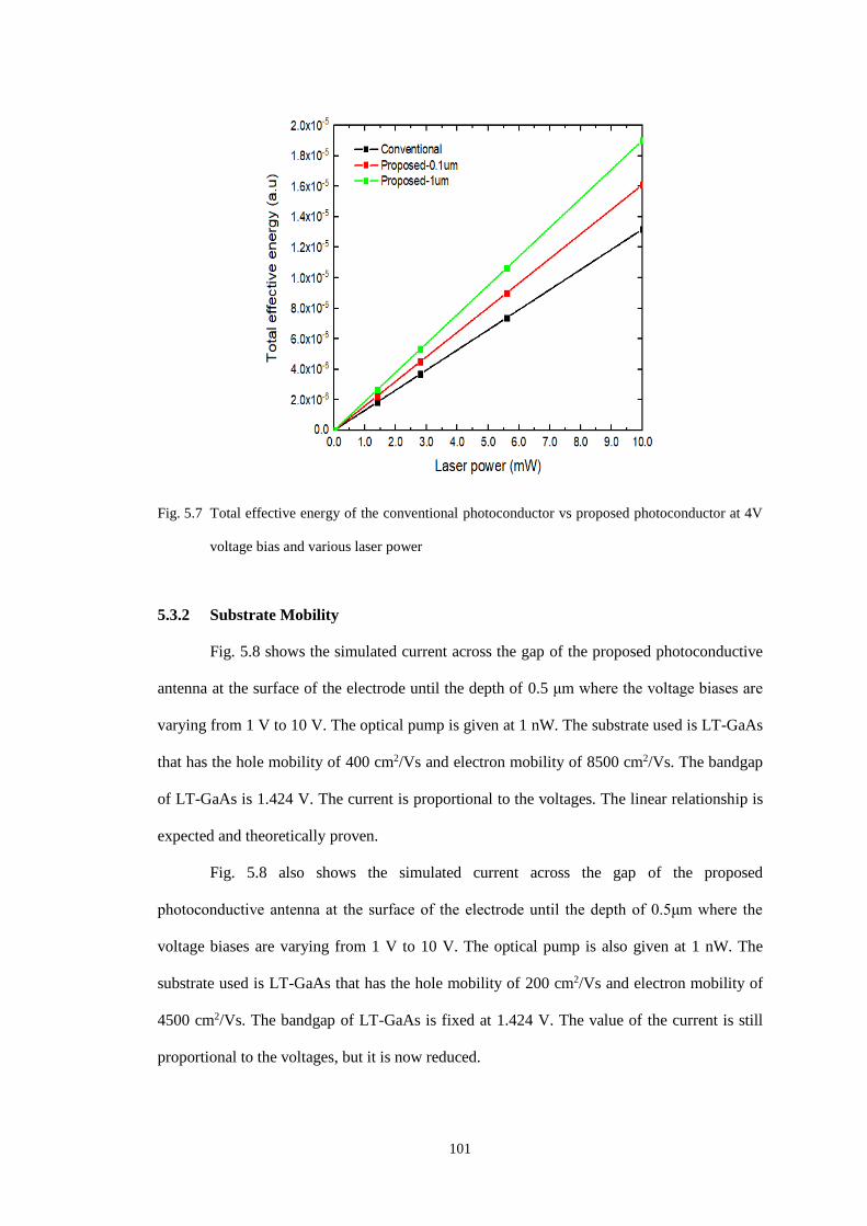
101
Fig. 5.7 Total effective energy of the conventional photoconductor vs proposed photoconductor at 4V
voltage bias and various laser power
5.3.2 Substrate Mobility
Fig. 5.8 shows the simulated current across the gap of the proposed photoconductive
antenna at the surface of the electrode until the depth of 0.5 μm where the voltage biases are
varying from 1 V to 10 V. The optical pump is given at 1 nW. The substrate used is LT-GaAs
that has the hole mobility of 400 cm2/Vs and electron mobility of 8500 cm2/Vs. The bandgap
of LT-GaAs is 1.424 V. The current is proportional to the voltages. The linear relationship is
expected and theoretically proven.
Fig. 5.8 also shows the simulated current across the gap of the proposed
photoconductive antenna at the surface of the electrode until the depth of 0.5μm where the
voltage biases are varying from 1 V to 10 V. The optical pump is also given at 1 nW. The
substrate used is LT-GaAs that has the hole mobility of 200 cm2/Vs and electron mobility of
4500 cm2/Vs. The bandgap of LT-GaAs is fixed at 1.424 V. The value of the current is still
proportional to the voltages, but it is now reduced.
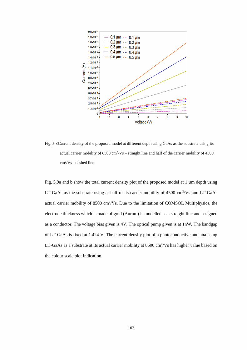
102
Fig. 5.8 Current density of the proposed model at different depth using GaAs as the substrate using its
actual carrier mobility of 8500 cm2/Vs – straight line and half of the carrier mobility of 4500
cm2/Vs - dashed line
Fig. 5.9a and b show the total current density plot of the proposed model at 1 µm depth using
LT-GaAs as the substrate using at half of its carrier mobility of 4500 cm2/Vs and LT-GaAs
actual carrier mobility of 8500 cm2/Vs. Due to the limitation of COMSOL Multiphysics, the
electrode thickness which is made of gold (Aurum) is modelled as a straight line and assigned
as a conductor. The voltage bias given is 4V. The optical pump given is at 1nW. The bandgap
of LT-GaAs is fixed at 1.424 V. The current density plot of a photoconductive antenna using
LT-GaAs as a substrate at its actual carrier mobility at 8500 cm2/Vs has higher value based on
the colour scale plot indication.
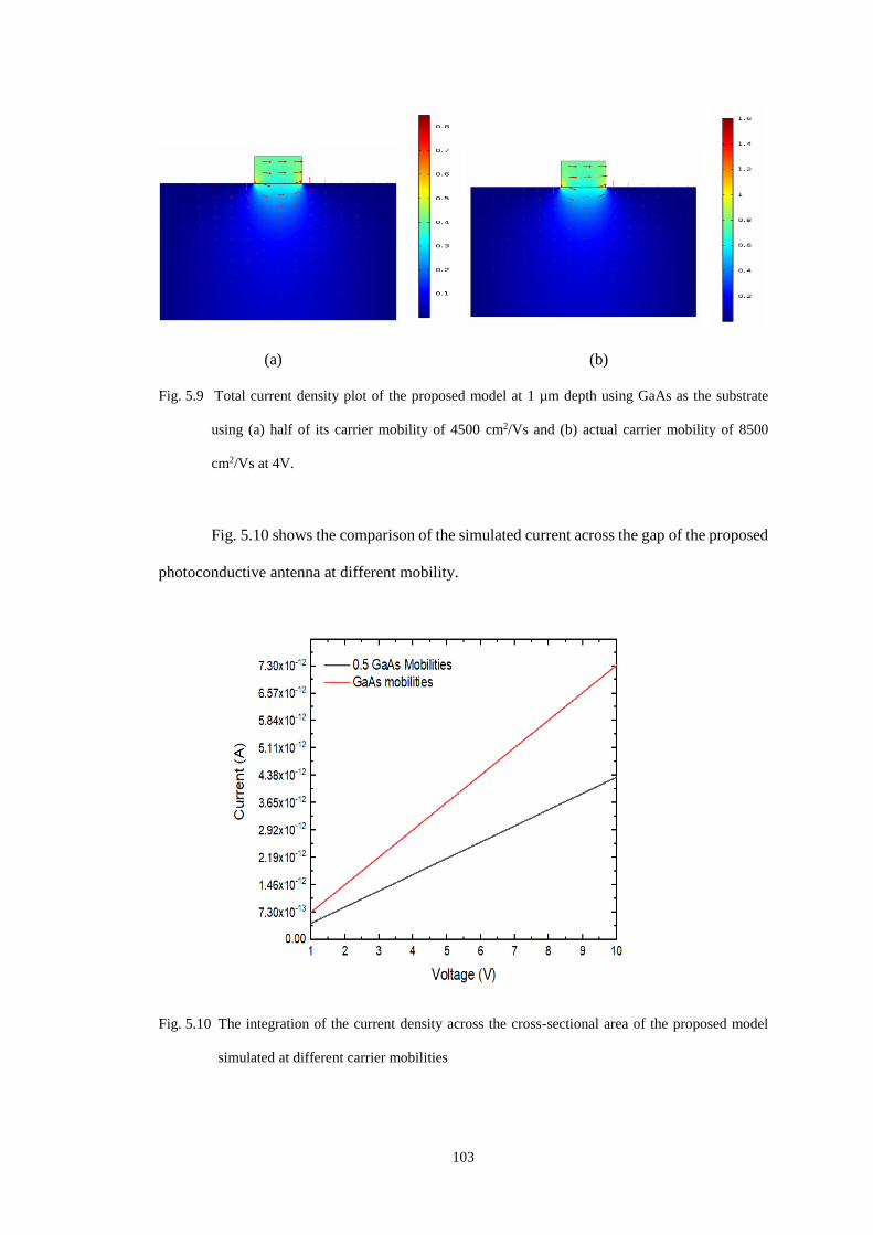
103
(a) (b)
Fig. 5.9 Total current density plot of the proposed model at 1 µm depth using GaAs as the substrate
using (a) half of its carrier mobility of 4500 cm2/Vs and (b) actual carrier mobility of 8500
cm2/Vs at 4V.
Fig. 5.10 shows the comparison of the simulated current across the gap of the proposed
photoconductive antenna at different mobility.
Fig. 5.10 The integration of the current density across the cross-sectional area of the proposed model
simulated at different carrier mobilities
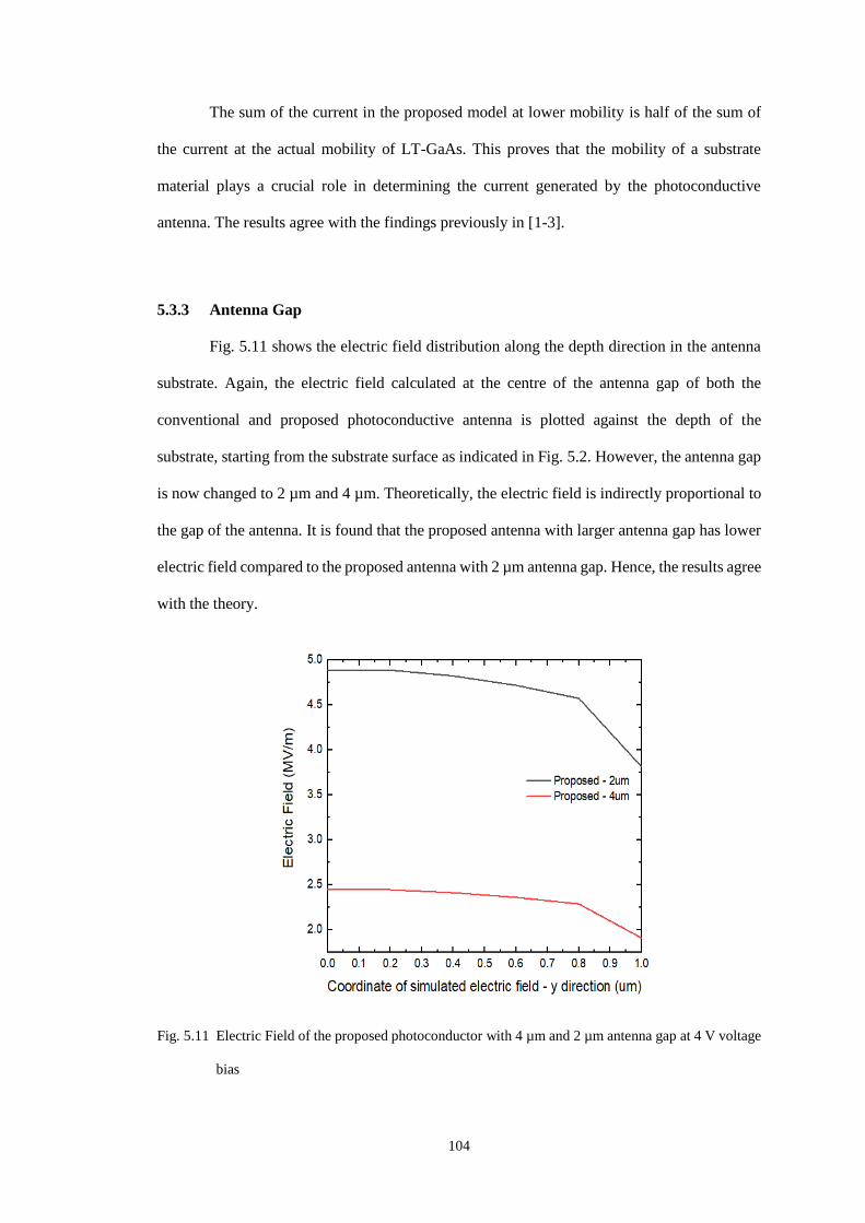
104
The sum of the current in the proposed model at lower mobility is half of the sum of
the current at the actual mobility of LT-GaAs. This proves that the mobility of a substrate
material plays a crucial role in determining the current generated by the photoconductive
antenna. The results agree with the findings previously in [1-3].
5.3.3 Antenna Gap
Fig. 5.11 shows the electric field distribution along the depth direction in the antenna
substrate. Again, the electric field calculated at the centre of the antenna gap of both the
conventional and proposed photoconductive antenna is plotted against the depth of the
substrate, starting from the substrate surface as indicated in Fig. 5.2. However, the antenna gap
is now changed to 2 µm and 4 µm. Theoretically, the electric field is indirectly proportional to
the gap of the antenna. It is found that the proposed antenna with larger antenna gap has lower
electric field compared to the proposed antenna with 2 µm antenna gap. Hence, the results agree
with the theory.
Fig. 5.11 Electric Field of the proposed photoconductor with 4 µm and 2 µm antenna gap at 4 V voltage
bias
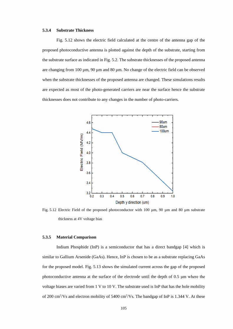
105
5.3.4 Substrate Thickness
Fig. 5.12 shows the electric field calculated at the centre of the antenna gap of the
proposed photoconductive antenna is plotted against the depth of the substrate, starting from
the substrate surface as indicated in Fig. 5.2. The substrate thicknesses of the proposed antenna
are changing from 100 µm, 90 µm and 80 µm. No change of the electric field can be observed
when the substrate thicknesses of the proposed antenna are changed. These simulations results
are expected as most of the photo-generated carriers are near the surface hence the substrate
thicknesses does not contribute to any changes in the number of photo-carriers.
Fig. 5.12 Electric Field of the proposed photoconductor with 100 µm, 90 µm and 80 µm substrate
thickness at 4V voltage bias
5.3.5 Material Comparison
Indium Phosphide (InP) is a semiconductor that has a direct bandgap [4] which is
similar to Gallium Arsenide (GaAs). Hence, InP is chosen to be as a substrate replacing GaAs
for the proposed model. Fig. 5.13 shows the simulated current across the gap of the proposed
photoconductive antenna at the surface of the electrode until the depth of 0.5 μm where the
voltage biases are varied from 1 V to 10 V. The substrate used is InP that has the hole mobility
of 200 cm2/Vs and electron mobility of 5400 cm2/Vs. The bandgap of InP is 1.344 V. At these
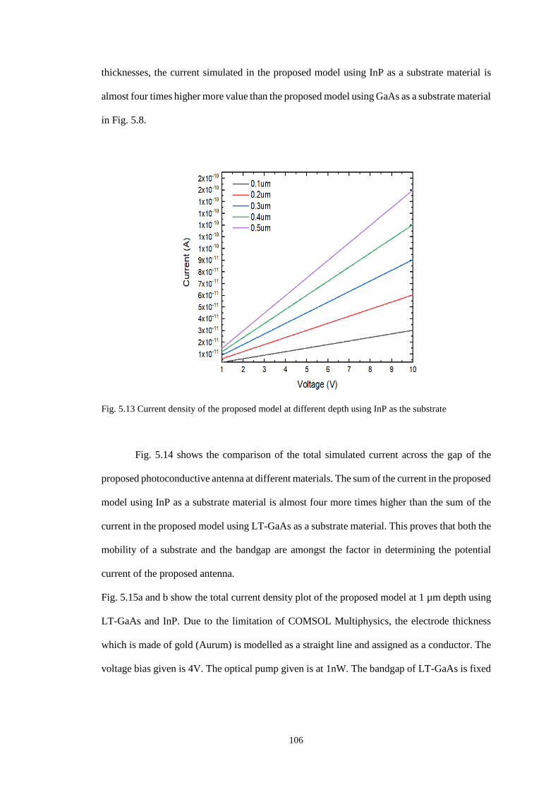
106
thicknesses, the current simulated in the proposed model using InP as a substrate material is
almost four times higher more value than the proposed model using GaAs as a substrate material
in Fig. 5.8.
Fig. 5.13 Current density of the proposed model at different depth using InP as the substrate
Fig. 5.14 shows the comparison of the total simulated current across the gap of the
proposed photoconductive antenna at different materials. The sum of the current in the proposed
model using InP as a substrate material is almost four more times higher than the sum of the
current in the proposed model using LT-GaAs as a substrate material. This proves that both the
mobility of a substrate and the bandgap are amongst the factor in determining the potential
current of the proposed antenna.
Fig. 5.15a and b show the total current density plot of the proposed model at 1 µm depth using
LT-GaAs and InP. Due to the limitation of COMSOL Multiphysics, the electrode thickness
which is made of gold (Aurum) is modelled as a straight line and assigned as a conductor. The
voltage bias given is 4V. The optical pump given is at 1nW. The bandgap of LT-GaAs is fixed
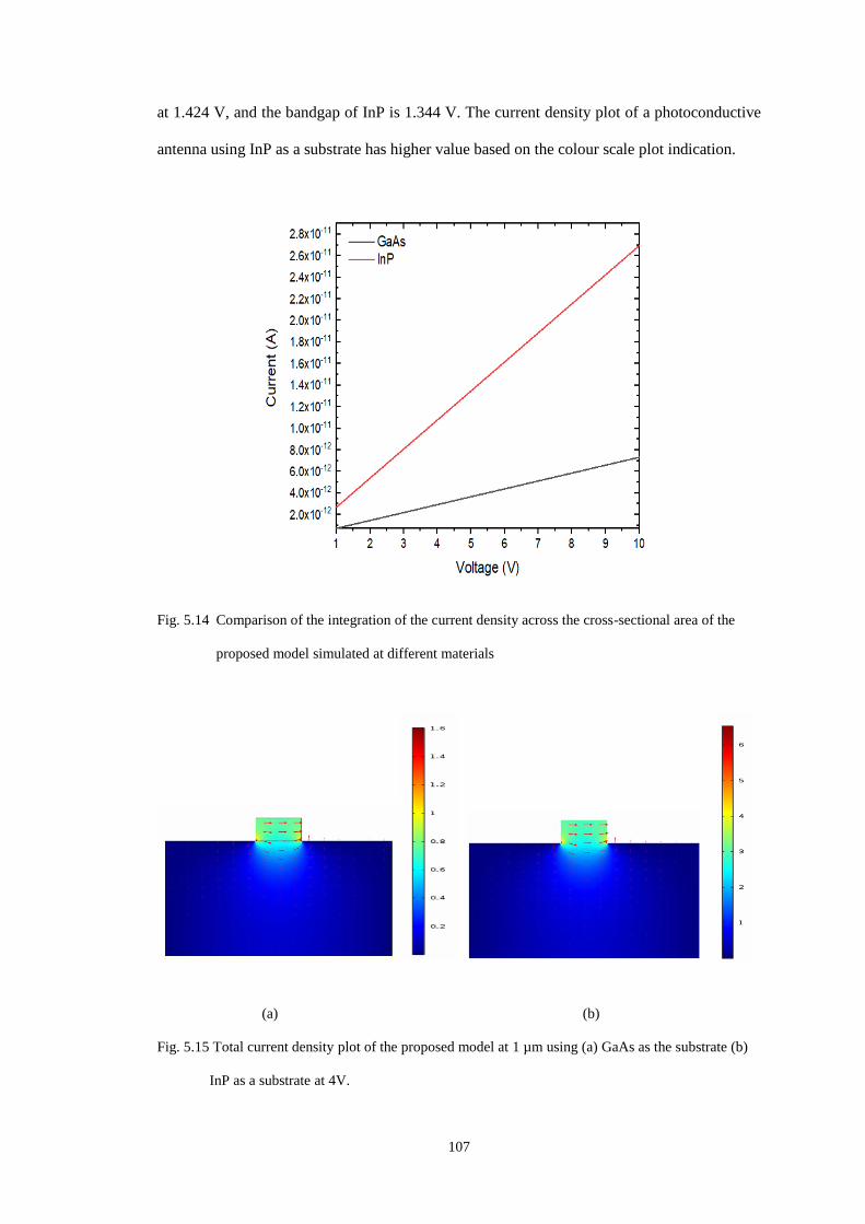
107
at 1.424 V, and the bandgap of InP is 1.344 V. The current density plot of a photoconductive
antenna using InP as a substrate has higher value based on the colour scale plot indication.
Fig. 5.14 Comparison of the integration of the current density across the cross-sectional area of the
proposed model simulated at different materials
(a) (b)
Fig. 5.15 Total current density plot of the proposed model at 1 µm using (a) GaAs as the substrate (b)
InP as a substrate at 4V.
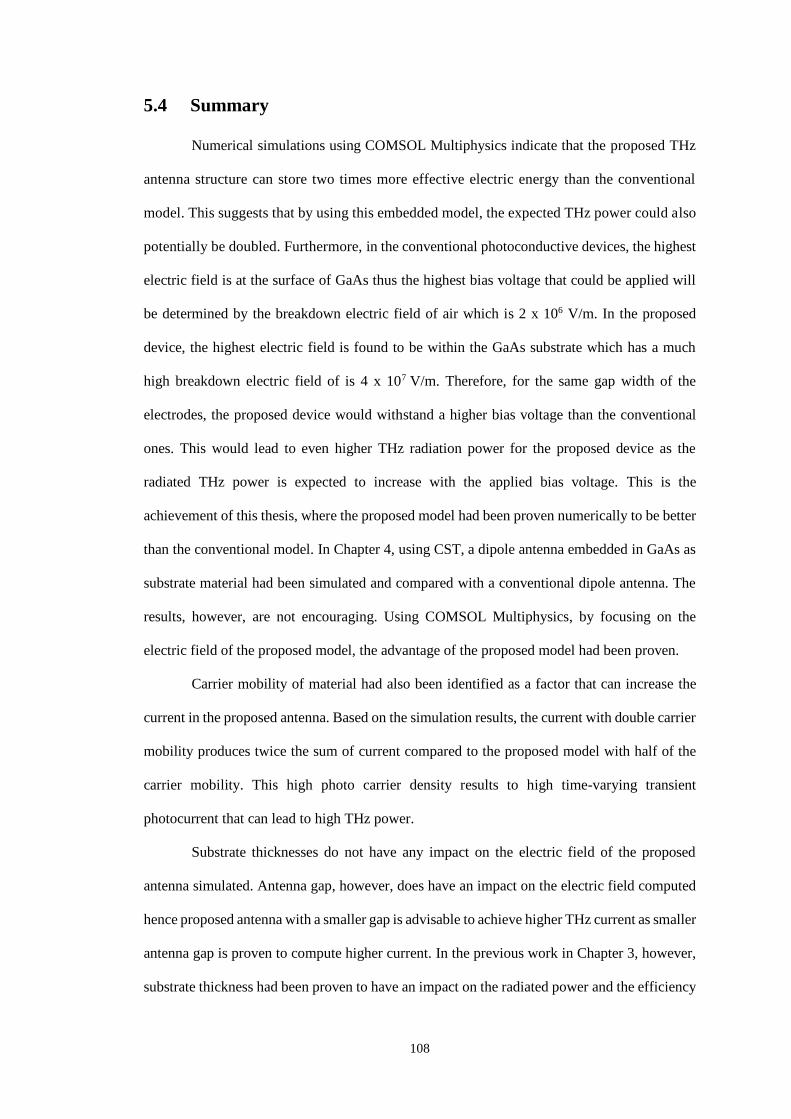
108
5.4 Summary
Numerical simulations using COMSOL Multiphysics indicate that the proposed THz
antenna structure can store two times more effective electric energy than the conventional
model. This suggests that by using this embedded model, the expected THz power could also
potentially be doubled. Furthermore, in the conventional photoconductive devices, the highest
electric field is at the surface of GaAs thus the highest bias voltage that could be applied will
be determined by the breakdown electric field of air which is 2 x 10⁶ V/m. In the proposed
device, the highest electric field is found to be within the GaAs substrate which has a much
high breakdown electric field of is 4 x 10⁷ V/m. Therefore, for the same gap width of the
electrodes, the proposed device would withstand a higher bias voltage than the conventional
ones. This would lead to even higher THz radiation power for the proposed device as the
radiated THz power is expected to increase with the applied bias voltage. This is the
achievement of this thesis, where the proposed model had been proven numerically to be better
than the conventional model. In Chapter 4, using CST, a dipole antenna embedded in GaAs as
substrate material had been simulated and compared with a conventional dipole antenna. The
results, however, are not encouraging. Using COMSOL Multiphysics, by focusing on the
electric field of the proposed model, the advantage of the proposed model had been proven.
Carrier mobility of material had also been identified as a factor that can increase the
current in the proposed antenna. Based on the simulation results, the current with double carrier
mobility produces twice the sum of current compared to the proposed model with half of the
carrier mobility. This high photo carrier density results to high time-varying transient
photocurrent that can lead to high THz power.
Substrate thicknesses do not have any impact on the electric field of the proposed
antenna simulated. Antenna gap, however, does have an impact on the electric field computed
hence proposed antenna with a smaller gap is advisable to achieve higher THz current as smaller
antenna gap is proven to compute higher current. In the previous work in Chapter 3, however,
substrate thickness had been proven to have an impact on the radiated power and the efficiency
109
of THz photoconductive antenna. The antenna was fed with a discrete port, due to the limitation
of CST. Hence, the results might not be accurate. In COMSOL, the fed of a THz
photoconductive antenna is emulated with both voltage bias and optical pump.
To achieve the wavelength of 780nm, the bandgap of the material chosen as substrate
material should be in the range of 1.3 V-1.4 V. As bandgap energy of a material is fixed, Indium
Phosphide (InP) is chosen as an alternative substrate material to LT-GaAs in order to investigate
the current’s result once the proposed model substrate material is changed to LT-GaAs. The
bandgap energy of InP is lower than LT-GaAs bandgap energy [5-7]. The photocurrent
simulated is found to be almost four times higher than the original proposed model using LT-
GaAs. Hence, as a conclusion, the electrode thickness and material mobility are among the
most crucial factor in determining the current of the proposed model.
110
References
[1] A. Abu Bakar Sajak, Y. Shen, Y. Huang, and R. Alrawashdeh, “A Comparison of the
Effect of Substrate on the Performance of THz Antenna”, Proceeding of the
ICE2T, Malaysia, August 2014.
[2] A. Abu Bakar Sajak, Y. Shen, Y. Huang, and R. Alrawashdeh, “An Investigation on
THz Antennas Using Graphene as a Substrate”, The 8th European Conference on
Antennas and Propagation, The Hague, The Netherlands, April 2014.
[3] N. Khiabani, “Modelling, design and characterisation of Terahertz photoconductive
antenna”. PhD thesis, University of Liverpool, 2013.
[4] A. Abu Bakar Sajak, Y. Shen and Y. Huang “Analysis of a Photoconductive Antenna
using COMSOL”, 10th UK-Europe-China Workshop on Milimetre Waves and
Terahertz Technologies (UCMMT), Liverpool, UK, September 2017.
[5] R. L. David, Handbook of Chemistry and Physics, 87th ed., CRC Press, pp. 4–61,.1998
[6] S. Adachi, Physical properties of III-V semiconductor compounds InP, InAs, GaAs,
GaP, InGaAs and InGaAsP, Wiley, New York, 1992
[7] G. Carpintero, et al., Semiconductor Terahertz Technology: Devices and Systems at
Room Temperature Operation, John Wiley & Sons, Incorporated, 2015.
111
Chapter 6 Conclusions and Future Work
6.1 Conclusions
THz photoconductive antenna consists of two metal usually gold electrodes on a
photoconductive substrate. Substrate effect in THz plays an important role compared to
substrate effect in microwave frequency. Chapter 3 investigated the impact of substrate
dimensions and substrate material on the performance of THz photoconductive antenna. The
investigations were done using CST simulation. At 1 THz, the efficiency and the radiated power
are the highest for a substrate thickness with the minimum size which is at 15 µm. Hence, the
dimensions of 150 µm x 150 µm x 15 µm had been used for as substrate dimensions for any
further study on a substrate material. Graphene, a promising material to be used as a substrate
for THz antennas had been found to radiate 33% more power than the THz antenna using GaAs
as a substrate at 0.5 THz – 0.7 THz.
In Chapter 4, the investigation centres on electrode structure and electrode material
study. The study of the radiated power of a dipole antenna using embedded electrode compared
to the dipole antenna using standard electrode is not very encouraging. Due to the limitations
of the CST Microwave Studio software wherein the student edition, only 30 000 mesh cells can
be simulated; another potential software needs to be reconsidered to prove the theory discussed
more accurately. This limitation also only allows a narrow frequency range. This semiconductor
physics equation should be combined with Maxwell’s equations in order to obtain the accurate
results of the expected radiated power of the THz photoconductive antenna. Also, the study of
the radiated power of a dipole antenna using noble materials such as gold (Aurum) and silver
112
(Argentum) with graphene and Titanium Nitride (TiN) proves that graphene performed better
than gold and silver due to its material properties such as higher carrier mobility.
In chapter 5, a novel photoconductive antenna with an embedded electrode structure,
rather than the conventional planner electrode structures had been introduced. Electric field
simulated using COMSOL Multiphysics proves that the proposed model performs better than
the conventional model. The electric field calculated at the centre of the gap between two
electrodes for both the conventional and the proposed photoconductive antenna is plotted
against the depth of the substrate, starting from the substrate surface. A higher electric field
over larger depth is observed for a thicker electrode of the proposed antenna. In contrast, no
change of the electric field can be observed when the electrode thicknesses of the conventional
antenna are changed. The new findings in Chapter 5, disputes the conclusions of Chapter 3,
where in Chapter 3 substrate thickness had been proven to have an impact on the radiated power
and the efficiency of THz photoconductive antenna. Due to the limitation of CST, the antenna
was fed with a discrete port. Hence, the results earlier might not be accurate.
The simulated electric field can be converted to the electric energy density. This stored
static electric power represents the maximum electric power that could potentially be converted
into THz radiation when the antenna device is excited with, for example, short laser pulses from
a femtosecond laser. The total effective energy stored in the conventional and proposed antenna
had then be calculated in COMSOL Multiphysics using the novel equation and the total
effective energy stored in the proposed antenna was found to be almost double than that in the
conventional antenna. The equation is inspired by the fact that the total electric current (I) can
be related to the current density (J) by integrating the current density over the area where a
charge is flowing, which in this case is the proposed model. Also, the current density can be
related to the electric field with its electric conductivity. Since LT-GaAs has non-zero
conductivity this electric field with produce a current. Experimental results of this proposed
antenna can prove these equations.
113
Besides the electrode thickness, substrate mobilities and antenna gap are among the
related parameters that had been identified and proven in this research to produce more
photocurrent hence possibility of higher radiated THz power. The integration of the current
density across the cross-sectional area in the proposed model at lower mobility is half of the
integration of the current density across the cross-sectional area in the proposed model at the
actual mobility of LT-GaAs. This proves that the mobility of a substrate material plays a crucial
role in determining the current generated by the photoconductive antenna.
In conclusion, the proposed THz photoconductive antenna had been proven
numerically to improve THz photocurrent compared to the conventional photoconductive.

114
6.2 Future Work
Photoconductive antennas (PCAs) are among the most popular devices used in THz
radiation emission and detection of THz radiation. Compare to other THz emitter and detector,
photoconductive antennas are compact, able to work in room temperature and they can work
both as an emitter and detector. However, due to their low optical-to-THz conversion
efficiencies, applications of these devices are limited. Extensive research had been done to
understand and identify the improvement that can be done in order to rectify the low optical-
to-THz conversion.
Using nanoplasmonic structures is very effective in improving the quantum efficiency
of photoconductive THz devices. The reason for this fact originates from the unique capability
of nanoplasmonic structures to enhance the absorption of incident laser pulses. Fabrication of
such structures, however, is difficult and costly. Hence, the equation proposed in this research
together with the simulation tool that combines both optoelectronic and electromagnetic
simulations is the approach which should be adopted for THz antenna analysis in order to a
predict the results of THz photocurrent and avoid any costly and unsuccessful experiment.
Though photoconductive antenna is basically consisting of simple electrode geometry
such as bow tie and dipole, with the proof of concept of an embedded electrode using both the
equation and simulation software, more robust and more complicated design can now be
implemented and simulated before proceeding with the experimental work. Table 6.1 shows
the suggested substrate dimensions, for THz Photoconductive Antenna based on the simulation
done throughout the thesis. The findings on Chapter 5, disputes the conclusions of Chapter 3,
where in Chapter 3 substrate thickness had been proven to have an impact on the radiated power
and the efficiency of THz photoconductive antenna.
Semiconductor as the substrate material of terahertz photoconductive antenna is one of
the main contributions of the THz radiation where high electron mobility is needed to obtain
strong THz signals, high intrinsic resistivity and high breakdown voltage in order to support
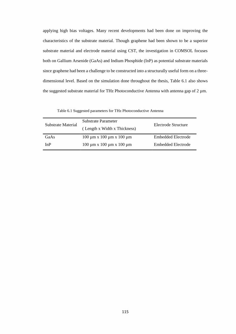
115
applying high bias voltages. Many recent developments had been done on improving the
characteristics of the substrate material. Though graphene had been shown to be a superior
substrate material and electrode material using CST, the investigation in COMSOL focuses
both on Gallium Arsenide (GaAs) and Indium Phosphide (InP) as potential substrate materials
since graphene had been a challenge to be constructed into a structurally useful form on a three-
dimensional level. Based on the simulation done throughout the thesis, Table 6.1 also shows
the suggested substrate material for THz Photoconductive Antenna with antenna gap of 2 µm.
Table 6.1 Suggested parameters for THz Photoconductive Antenna
Substrate Material Substrate Parameter
( Length x Width x Thickness) Electrode Structure
GaAs 100 µm x 100 µm x 100 µm Embedded Electrode
InP 100 µm x 100 µm x 100 µm Embedded Electrode
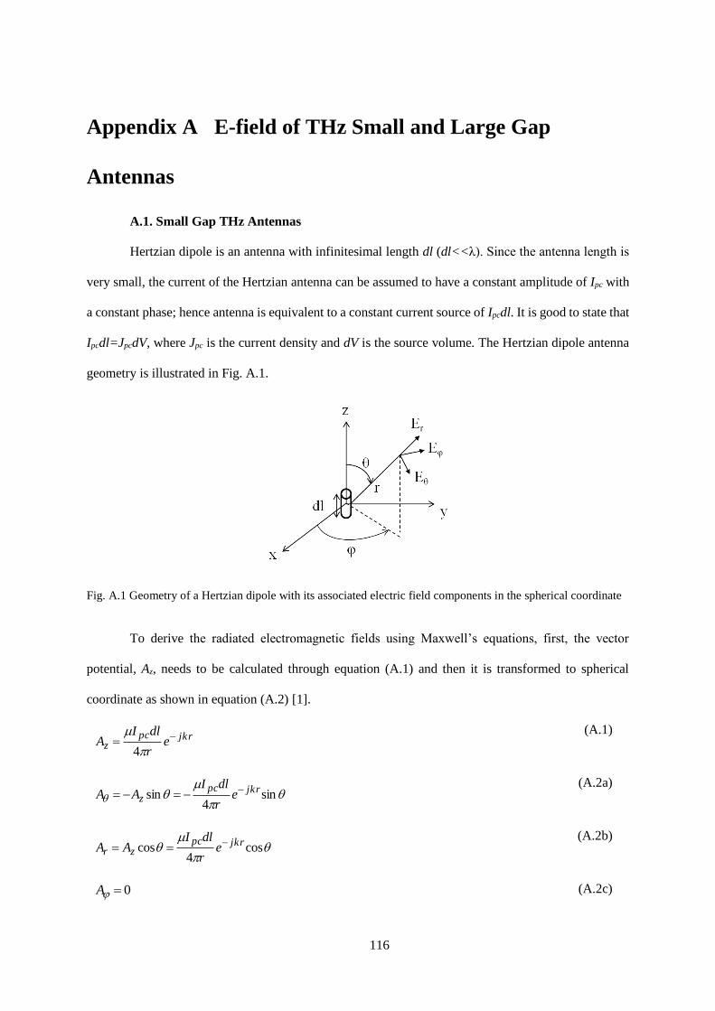
116
Appendix A E-field of THz Small and Large Gap
Antennas
A.1. Small Gap THz Antennas
Hertzian dipole is an antenna with infinitesimal length dl (dl<<λ). Since the antenna length is
very small, the current of the Hertzian antenna can be assumed to have a constant amplitude of Ipc with
a constant phase; hence antenna is equivalent to a constant current source of Ipcdl. It is good to state that
Ipcdl=JpcdV, where Jpc is the current density and dV is the source volume. The Hertzian dipole antenna
geometry is illustrated in Fig. A.1.
Fig. A.1 Geometry of a Hertzian dipole with its associated electric field components in the spherical coordinate
To derive the radiated electromagnetic fields using Maxwell’s equations, first, the vector
potential, Az, needs to be calculated through equation (A.1) and then it is transformed to spherical
coordinate as shown in equation (A.2) [1].
(A.1)
(A.2a)
(A.2b)
(A.2c)
jkrpcz e
r
dlIA
4
sin
4sin jkrpc
z er
dlIAA
cos
4cos jkrpc
zr er
dlIAA
0A
117
here μ is the permeability, is the wave number and r is the observation distance.
Considering the relations of electric and magnetic fields with the vector potential according to equation
(A.3),
(A.3a)
(A.3b)
Electric, E, and magnetic, H, fields can be calculated as presented in (A.4):
(A.4a)
(A.4b)
(A.4c)
, , (A.4d)
where are the intrinsic impedance and ε is the permittivity.
In THz photoconductive antennas, time domain behaviour of fields is used. Therefore, by
multiplying field components of equation (A.4) with ejωt, getting the real part of fields and considering
the time difference between the observation point and source point as (c is the light velocity),
time domain equations of the fields of equation (A.4) can be obtained by (A.5).
(A.5a)
(A.5b)
(A.5c)
2k
AH
1
HjE
jkrpce
krj
r
dlkIH
1sin
4
jkrpce
kr
j
krj
r
dlkIE
2)(
1sin
4
jkrpcr e
jkrr
dlkIE
11cos
2 2
0rH 0H 0E
c
rttd
2
cossinsin
4
~
r
t
rc
tdlIH ddpc
322
sincossinsin
4
~
r
t
cr
t
rc
tdlIE dddpc
32
sincoscos
2
~
r
t
cr
tdlIE ddpc
r
118
From equation (A.5) it can be interpreted that and are radiative components in the far field
(kr>>1) since they have the factor of 1/r. Assuming that Ipc(td) = Ipc cosωtd and considering the relation
between charge and current , equations (A.5a) and (A.5b) can be rewritten as (A.6a) and
(A.6b) respectively:
(A.6a)
(A.6b)
Thus, the radiated electric field is proportional to the time derivative of the current (or
equivalently it is proportional to the current density).
It is good to mention that in previous work in the literature, the relation of radiated THz power
to the current was explained through Hertz vector potential of a time-varying dipole moment [34, 68]
which is a popular method in areas like quantum electronics and solid-state physics. However, here this
relation was explained through the usage of vector potential and considering the time-varying behaviour
of the Hertzian dipole as an antenna.
A.2. Large-Aperture THz Antennas
The geometry of a large-aperture THz antenna is shown in Fig. A.2. Spectral and temporal
format of emission of THz radiation from this antenna according to Maxwell's equations can be written
as [84]:
(A.7a)
(A.7b)
E~
H~
t
qtI pc
)(
)(sin4
)(sin
4
~2 dpc
d
dpctI
r
dl
t
tI
rc
dlH
ddpc
d
dpc
t
q
r
dltI
cr
dl
t
tI
rc
dlE
sin
4)(sin
4
)(sin
4
~322
AjETHz
dt
tJd
z
S
r
dS
t
tJtrE ss
THz)(
4
)(
4),(
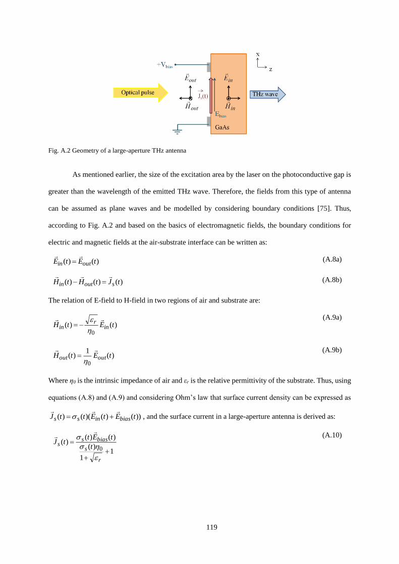
119
Fig. A.2 Geometry of a large-aperture THz antenna
As mentioned earlier, the size of the excitation area by the laser on the photoconductive gap is
greater than the wavelength of the emitted THz wave. Therefore, the fields from this type of antenna
can be assumed as plane waves and be modelled by considering boundary conditions [75]. Thus,
according to Fig. A.2 and based on the basics of electromagnetic fields, the boundary conditions for
electric and magnetic fields at the air-substrate interface can be written as:
(A.8a)
(A.8b)
The relation of E-field to H-field in two regions of air and substrate are:
(A.9a)
(A.9b)
Where η0 is the intrinsic impedance of air and εr is the relative permittivity of the substrate. Thus, using
equations (A.8) and (A.9) and considering Ohm’s law that surface current density can be expressed as
, and the surface current in a large-aperture antenna is derived as:
(A.10)
)()( tEtE outin
)()()( tJtHtH soutin
)()(0
tEtH inr
in
)(1
)(0
tEtH outout
))()()(()( tEtEttJ biasinss
11
)(
)()()(
0
r
s
biasss t
tEttJ
120
Appendix B Calculation of efficiencies
The average photocurrent Iavp and approximate photoconductive resistance Rapp are considered as
equations (B.1) and (B.2) respectively:
(B.1)
(B.2)
where Vbias is the bias voltage, L is the antenna gap length, and Pav is the average optical power. Then,
the optical-to-electrical efficiency can be estimated as:
(B.3)
Considering some typical values as
μe = 1000 cm2.V-1.s-1
c = 0.5 ps
Vbias = 30 V
Pav = 50 mW
L = 5 μm
trep = 1/80 μs
h = 6.626 x 10⁻³⁴ J.s
e = 3 x 10⁻⁸ ms-1
c = 1.6 x 10⁻¹⁹ C
f = 375 THz
in equation (B.3), η1p = 7.2 × 10⁻⁵.
The matching efficiency can be calculated according to equation (B.4) for a half-wavelength dipole
antenna on a substrate with εr = 12.9. Assuming the antenna resistance in free space, Zfree, is 73 Ω and
2hfL
PVeI avbiasceavp
repaveapp
tPe
hfLR
2
3 2
2
222
12
3
hfLt
Ve
P
IR
rep
biasce
av
avpappp
121
by using the above values in equation (B.2) Rapp is 0.89 Ω, then the matching efficiency will be η2p =
0.16.
(B.4)
Assuming also that a radiation efficiency η3p of can be relatively high, typically over 80%, the total
antenna efficiency for this sample, which is a multiplication of efficiencies from three described
processes, is calculated as 5.7 × 10⁻⁶.
2
2 1apprfree
apprfreep
RZ
RZ


![Terahertz spectrum analyzer based on a terahertz frequency ...heterodyning photoconductive detection [9]. Since this so-called THz comb is a harmonic comb of the laser mode-locked](https://img.pdfslide.net/doc/110x75/5f09c7dd7e708231d42876f2/terahertz-spectrum-analyzer-based-on-a-terahertz-frequency-heterodyning-photoconductive.jpg)