Embed Size (px)
Citation preview
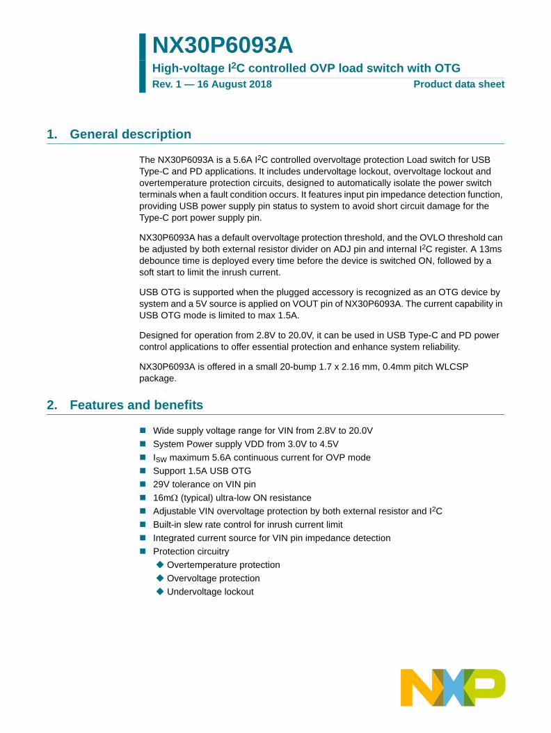
1. General description
The NX30P6093A is a 5.6A I2C controlled overvoltage protection Load switch for USB Type-C and PD applications. It includes undervoltage lockout, overvoltage lockout and overtemperature protection circuits, designed to automatically isolate the power switch terminals when a fault condition occurs. It features input pin impedance detection function, providing USB power supply pin status to system to avoid short circuit damage for the Type-C port power supply pin.
NX30P6093A has a default overvoltage protection threshold, and the OVLO threshold can be adjusted by both external resistor divider on ADJ pin and internal I2C register. A 13ms debounce time is deployed every time before the device is switched ON, followed by a soft start to limit the inrush current.
USB OTG is supported when the plugged accessory is recognized as an OTG device by system and a 5V source is applied on VOUT pin of NX30P6093A. The current capability in USB OTG mode is limited to max 1.5A.
Designed for operation from 2.8V to 20.0V, it can be used in USB Type-C and PD power control applications to offer essential protection and enhance system reliability.
NX30P6093A is offered in a small 20-bump 1.7 x 2.16 mm, 0.4mm pitch WLCSP package.
2. Features and benefits
Wide supply voltage range for VIN from 2.8V to 20.0V
System Power supply VDD from 3.0V to 4.5V
ISW maximum 5.6A continuous current for OVP mode
Support 1.5A USB OTG
29V tolerance on VIN pin
16m (typical) ultra-low ON resistance
Adjustable VIN overvoltage protection by both external resistor and I2C
Built-in slew rate control for inrush current limit
Integrated current source for VIN pin impedance detection
Protection circuitry
Overtemperature protection
Overvoltage protection
Undervoltage lockout
NX30P6093AHigh-voltage I2C controlled OVP load switch with OTGRev. 1 — 16 August 2018 Product data sheet
NXP Semiconductors NX30P6093AHigh-voltage I2C controlled OVP load switch with OTG
Surge protection:
IEC61000-4-5 exceeds ±100V on VIN
ESD protection
IEC61000-4-2 contact discharge exceeds 8kV on VIN
IEC61000-4-2 air discharge exceeds 15kV on VIN
HBM ANSI/ESDA/JEDEC JS-001 Class 2 exceeds 3kV on all pins
MM Class B exceeds 100 V on all the pins
Specified from -40 °C to +85 °C
3. Applications
Smart and feature phones
Tablets, eBooks
Notebook
4. Ordering information
4.1 Ordering options
5. Marking
Table 1. Ordering information
Type number Package
Temperature range
Name Description Version
NX30P6093AUK 40 C to +85 C WLCSP20 wafer level chip-scale package; 20 bumps; 1.70 mm x 2.16 mm x 0.525 mm body (backside coating included)
SOT1397-6
Table 2. Ordering options
Type number Orderable part number
Package Packing method Minimum order quantity
Temperature
NX30P6093AUK NX30P6093AUKZ WLCSP20 REEL 7" Q1/T1 *SPECIAL MARK CHIPS DP
4000 Tamb = 40 C to +85 C
Table 3. Marking
Line Marking Description
1 X30AP2 basic type name
NX30P6093A All information provided in this document is subject to legal disclaimers. © NXP B.V. 2018. All rights reserved.
Product data sheet Rev. 1 — 16 August 2018 2 of 33
NXP Semiconductors NX30P6093AHigh-voltage I2C controlled OVP load switch with OTG
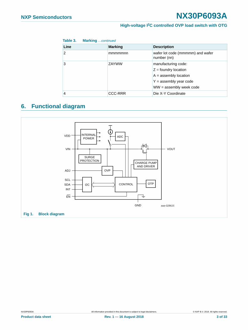
6. Functional diagram
2 mmmmmnn wafer lot code (mmmmm) and wafer number (nn)
3 ZAYWW manufacturing code:
Z = foundry location
A = assembly location
Y = assembly year code
WW = assembly week code
4 CCC-RRR Die X-Y Coordinate
Table 3. Marking …continued
Line Marking Description
Fig 1. Block diagram
aaa-028615
SURGEPROTECTION
CONTROL OTP
CHARGE PUMPAND DRIVER
VIN VOUT
SCLSDA
EN
GND
VDD
OVPADJ
ADC
INT
INTERNALPOWER
I2C
NX30P6093A All information provided in this document is subject to legal disclaimers. © NXP B.V. 2018. All rights reserved.
Product data sheet Rev. 1 — 16 August 2018 3 of 33
NXP Semiconductors NX30P6093AHigh-voltage I2C controlled OVP load switch with OTG
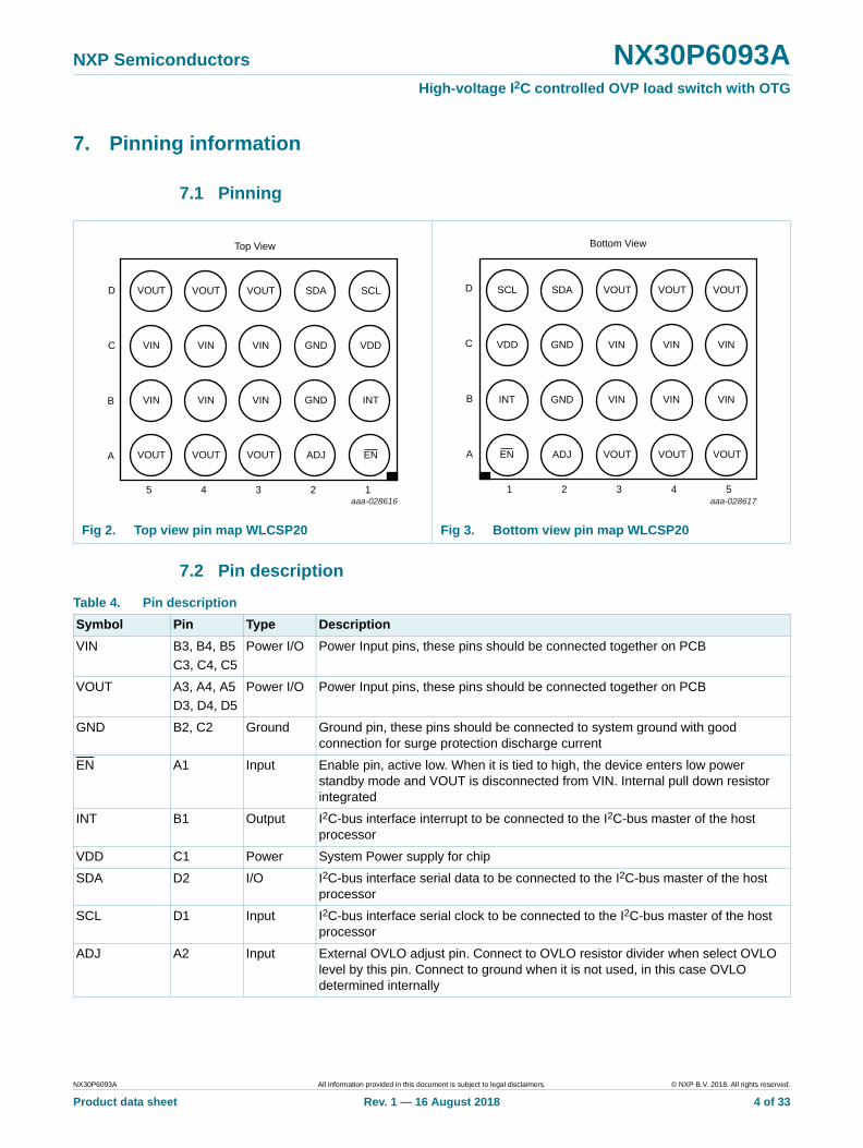
7. Pinning information
7.1 Pinning
7.2 Pin description
Fig 2. Top view pin map WLCSP20 Fig 3. Bottom view pin map WLCSP20
aaa-028616
SCL
VDD
INT
SDA
GND
GND
VOUT
VIN
VIN
VOUT
VIN
VIN
VOUT
VIN
VIN
ENADJVOUTVOUTVOUT
12345
A
B
C
D
Top View
aaa-028617
SCL
VDD
INT
SDA
GND
GND
VOUT
VIN
VIN
VOUT
VIN
VIN
VOUT
VIN
VIN
EN ADJ VOUT VOUT VOUT
1 2 3 4 5
A
B
C
D
Bottom View
Table 4. Pin description
Symbol Pin Type Description
VIN B3, B4, B5
C3, C4, C5
Power I/O Power Input pins, these pins should be connected together on PCB
VOUT A3, A4, A5
D3, D4, D5
Power I/O Power Input pins, these pins should be connected together on PCB
GND B2, C2 Ground Ground pin, these pins should be connected to system ground with good connection for surge protection discharge current
EN A1 Input Enable pin, active low. When it is tied to high, the device enters low power standby mode and VOUT is disconnected from VIN. Internal pull down resistor integrated
INT B1 Output I2C-bus interface interrupt to be connected to the I2C-bus master of the host processor
VDD C1 Power System Power supply for chip
SDA D2 I/O I2C-bus interface serial data to be connected to the I2C-bus master of the host processor
SCL D1 Input I2C-bus interface serial clock to be connected to the I2C-bus master of the host processor
ADJ A2 Input External OVLO adjust pin. Connect to OVLO resistor divider when select OVLO level by this pin. Connect to ground when it is not used, in this case OVLO determined internally
NX30P6093A All information provided in this document is subject to legal disclaimers. © NXP B.V. 2018. All rights reserved.
Product data sheet Rev. 1 — 16 August 2018 4 of 33
NXP Semiconductors NX30P6093AHigh-voltage I2C controlled OVP load switch with OTG
8. Functional description
NX30P6093A is an integrated device with three major functions: programmable overvoltage protection, VIN pin impedance detection and USB OTG. It protects USB Type-C power supply pin and internal system by isolating high voltage when it is exceeds OVLO threshold. The VIN pin impedance detection provides a status monitoring for system to avoid damage by short circuit of USB Type-C power supply pin.
The impedance detection feature is activated when VIN <VUVLO, in this case NX30P6093A supplied by system power VDD. When VIN>VUVLO, this feature is disabled automatically.
USB OTG is supported when the plugged accessory is recognized as an OTG device by system and a 5V source is applied on VOUT pin of NX30P6093A.
8.1 EN input
A HIGH on EN disables the channel MOSFET, all protection circuits, and VIN impedance detection circuits, putting the device into a low power mode. A LOW on EN enables the protection circuits and the MOSFET. There is an internal 1 M pull-down resistor on the EN pin to ensure the power switch conducting in a dead-battery situation. A 13ms debounce time has been deployed before device turning on.
8.2 OTG Mode
USB OTG is supported when the plugged accessory is recognized as an OTG device by system and a 5V source is applied on VOUT pin of NX30P6093A. The EN pin and VOUT_EN bit in register 0x01 must to be set LOW to support USB OTG mode. If EN pin or VOUT_EN bit is HIGH, the current is conducted by body diode that will induce much higher power dissipation due to body diode forward voltage and more heating in NX30P6093A. The overtemperature protection will not disable the main switch for the same reason, but only report interrupt to system. In this case, the system should turn off the power source of USB OTG to protect the device and system.
8.3 Slew Rate Tune
The slew rate control is integrated to avoid inrush current when the load switch turns on. It protects the internal circuits or blocks follow NX30P6093A. In order to increase the design flexibility on system level, the slew rate can be tuned through I2C through register 0x0F as follows:
Table 5. Slew rate tune setting by I2C register
Register Value SRT[2:0] Switch turn on slew rate (TYP)
000 0.42ms
001 0.44ms
010 0.5ms
011 0.65ms
100 0.9ms (Default)
101 1.5ms
110 2.8ms
111 5.6ms
NX30P6093A All information provided in this document is subject to legal disclaimers. © NXP B.V. 2018. All rights reserved.
Product data sheet Rev. 1 — 16 August 2018 5 of 33
NXP Semiconductors NX30P6093AHigh-voltage I2C controlled OVP load switch with OTG
8.4 Undervoltage lockout
When EN is LOW and VIN < VUVLO, the Undervoltage Lockout (UVLO) circuit disables the power MOSFET. Once VIN exceeds VUVLO, if no other protection circuit is active and EN is LOW, the MOSFET is turned on automatically regardless of the status of VOUT_EN in register 0x01h. If EN is HIGH, the MOSFET remains at off and at low power mode.
8.5 Overvoltage lockout
When EN is LOW and VIN > VOVLO, the overvoltage lockout (OVLO) circuit disables the power MOSFET. The OV_FLG in register 0x03h is set as “1” and an interrupt is issued to notify the host. Once VIN drops below VOVLO and no other protection circuit is active, the power MOSFET resumes operation.
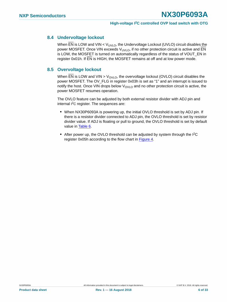
The OVLO feature can be adjusted by both external resistor divider with ADJ pin and internal I2C register. The sequences are:
• When NX30P6093A is powering up, the initial OVLO threshold is set by ADJ pin. If there is a resistor divider connected to ADJ pin, the OVLO threshold is set by resistor divider value. If ADJ is floating or pull to ground, the OVLO threshold is set by default value in Table 6.
• After power up, the OVLO threshold can be adjusted by system through the I2C register 0x05h according to the flow chart in Figure 4.
NX30P6093A All information provided in this document is subject to legal disclaimers. © NXP B.V. 2018. All rights reserved.
Product data sheet Rev. 1 — 16 August 2018 6 of 33
NXP Semiconductors NX30P6093AHigh-voltage I2C controlled OVP load switch with OTG
When the overvoltage threshold is set by the ADJ pin with the connected resistor divider (see Figure 7), the overvoltage threshold is adjustable from 4V to 23V with below equation
(1)
If the voltage on ADJ pin is below 0.1V, the device uses internal default OVLO threshold.
When the overvoltage threshold is set by system through I2C-bus, it is set by bit0 and bit1 of register 0x05h. The OVLO thresholds are shown in Table 6.
In additional, NX30P6093A provides two additional OVLO thresholds by bit0, bit1 of register 0x0Eh. The additional OVLO thresholds are shown in Table 7.
Fig 4. OVLO setting flow chart
Table 6. OVLO threshold setting by I2C register
Register Value OV[1:0] OVLO Threshold
00 6.8V (default)
01 11.5V
10 17V
11 23V
aaa-028640
Power-up
Resistor dividerconnected to ADJ?
N
Y
Y
N
Set OVLO accordingto ADJ pin resistor
divider value
ADJ is GND or floating, set OVLO
according to default value
If host wants to program OVLO, write the bit of OV[1:0] and
RNG[2:0]
OV_SEL=1?
Set OVLO level by I2C register 0x02h
Vovlo Vth ovlo R1 R2+ R2 =
NX30P6093A All information provided in this document is subject to legal disclaimers. © NXP B.V. 2018. All rights reserved.
Product data sheet Rev. 1 — 16 August 2018 7 of 33
NXP Semiconductors NX30P6093AHigh-voltage I2C controlled OVP load switch with OTG
Furthermore when the OVLO threshold is set by I2C register, it can be fine tuned by bit6-bit4 of register 0x05h. The fine tune values are shown in Table 8.
8.6 Overtemperature protection
When EN is LOW and the device temperature exceeds 140 °C the Overtemperature protection (OTP) circuit disables the power MOSFET and an interrupt is issued by setting OT_FLG as “1” in register 0x03h. Once the device temperature decreases below 120 °C and no other protection circuit is active, the state of the N-channel MOSFET is controlled by the EN pin again.
8.7 Short circuit protection
NX30P6093A has short circuit protection; after the MOSFET is fully turned on and when the current through it exceeds 10.5A typically, it turns the MOSFET off to protect the device and system. An interrupt is issued when short circuit protection is triggered by setting OC_FLG as “1” in register 0x03h. Once the short circuit condition is removed and no other protection circuit is active, the state of the N-channel MOSFET is controlled by the EN pin again.
8.8 VIN impedance detection
An VIN impedance detection function is integrated in NX30P6093A. When EN is LOW and VIN <VUVLO, NX30P6093A enters VIN detection sleep mode. The host can start the VIN impedance detection according to the following sequences. First, the host can write DETC_EN bit to “1” through I2C, activating NX30P6093A to VIN detection standby mode. In this mode, NX30P6093A turns on internal function circuits and is ready to run detection. After a wake up time tWAKEUP, the host can configure tDET, tDUTY and Tag voltage by writing the register 0x07h and 0x09h through I2C. When Isource is changed from default 0A to any of valid current values in Table 8, NX30P6093A starts the VIN detection according to configured tDET and tDUTY time.
Table 7. Additional OVLO threshold setting by I2C register
Register Value AOVP[1:0] OVLO Threshold
00 OVLO set by Table 6.
01 OVLO set by Table 6.
10 10V
11 14V
Table 8. OVLO threshold fine tune setting by I2C register
Register Value RNG[2:0] OVLO Threshold Fine Tune value
000 -600mV
001 -400mV
010 -200mV
011 0mV (default)
100 +200mV
101 +400mV
110 +600mV
111 +800mV
NX30P6093A All information provided in this document is subject to legal disclaimers. © NXP B.V. 2018. All rights reserved.
Product data sheet Rev. 1 — 16 August 2018 8 of 33
NXP Semiconductors NX30P6093AHigh-voltage I2C controlled OVP load switch with OTG
In any of VIN detection modes, while a VIN is plugged and the voltage on VIN pin exceeds VUVLO, NX30P6093A will exit from VIN detection modes to OVP operation modes immediately.
When the VIN detection ADC result is valid after tDET timer out, the TMR_OUT_STS is set to “1” and an interrupt is issued. The host can read the VIN detection voltage at register 0x08h by then. Meanwhile, NX30P6093A can compare the detection result versus the host set VIN TAG voltage in register 0x09h. When the detected voltage is less than the set VIN TAG voltage, the OVER_TAG_STS is set to “1” in register 0x02h and an interrupt is issued.
The VIN pin impedance can be the following two different cases according to the application in system,
• When there is no resistor divider connected to VIN and ADJ pins, the measured impedance (RM) is VIN impedance (RP).
• When an OVLO resistor divider is connected to VIN and ADJ pins, the measured impedance (RM) is VIN impedance (RP) parallels with external OVLO resistor divider R1+R2, (see Figure 7).
Table 9 shows the current source values, which can be programmed by bit3-bit0 of register 0x06h. Please be note there are several internal circuits connected to VIN pin, for example, Surge protection and UVLO resistor ladder. That generates a leakage current according to different VIN voltage specified in Table 28 as IDET_LEACKAGE. This leakage should be excluded in the resistor calculation of VIN impedance detection.
NX30P6093A turns on the Isource according to the following system required timing sequence.
Table 9. Current source set by I2C register
Register Value ISRC[3:0] Current source value
0000 0A (default)
0001 1A
0010 2A
0011 3A
0100 4A
0101 5A
0110 10A
0111 20A
1000 50A
1001 100A
1010 200A
1011 500A
1100 1000A
1101 2000A
1110 5000A
1111 10000A
NX30P6093A All information provided in this document is subject to legal disclaimers. © NXP B.V. 2018. All rights reserved.
Product data sheet Rev. 1 — 16 August 2018 9 of 33
NXP Semiconductors NX30P6093AHigh-voltage I2C controlled OVP load switch with OTG
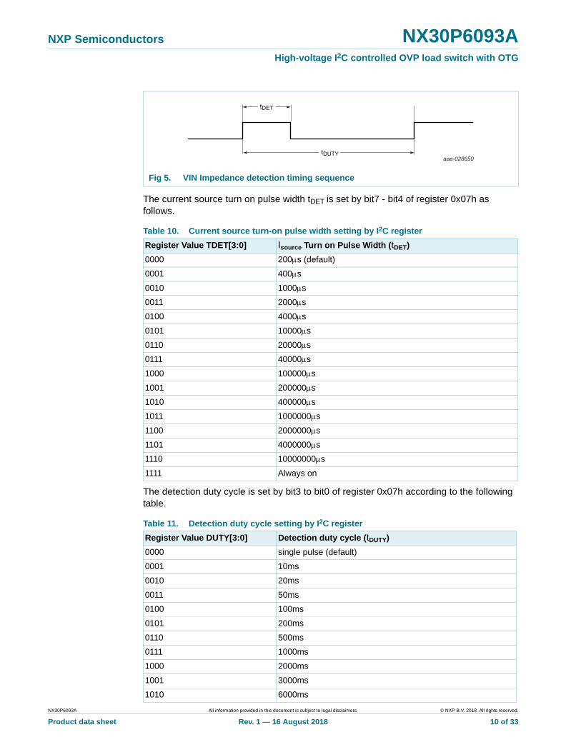
The current source turn on pulse width tDET is set by bit7 - bit4 of register 0x07h as follows.
The detection duty cycle is set by bit3 to bit0 of register 0x07h according to the following table.
Fig 5. VIN Impedance detection timing sequence
Table 10. Current source turn-on pulse width setting by I2C register
Register Value TDET[3:0] Isource Turn on Pulse Width (tDET)
0000 200s (default)
0001 400s
0010 1000s
0011 2000s
0100 4000s
0101 10000s
0110 20000s
0111 40000s
1000 100000s
1001 200000s
1010 400000s
1011 1000000s
1100 2000000s
1101 4000000s
1110 10000000s
1111 Always on
Table 11. Detection duty cycle setting by I2C register
Register Value DUTY[3:0] Detection duty cycle (tDUTY)
0000 single pulse (default)
0001 10ms
0010 20ms
0011 50ms
0100 100ms
0101 200ms
0110 500ms
0111 1000ms
1000 2000ms
1001 3000ms
1010 6000ms
aaa-028650
tDET
tDUTY
NX30P6093A All information provided in this document is subject to legal disclaimers. © NXP B.V. 2018. All rights reserved.
Product data sheet Rev. 1 — 16 August 2018 10 of 33
NXP Semiconductors NX30P6093AHigh-voltage I2C controlled OVP load switch with OTG
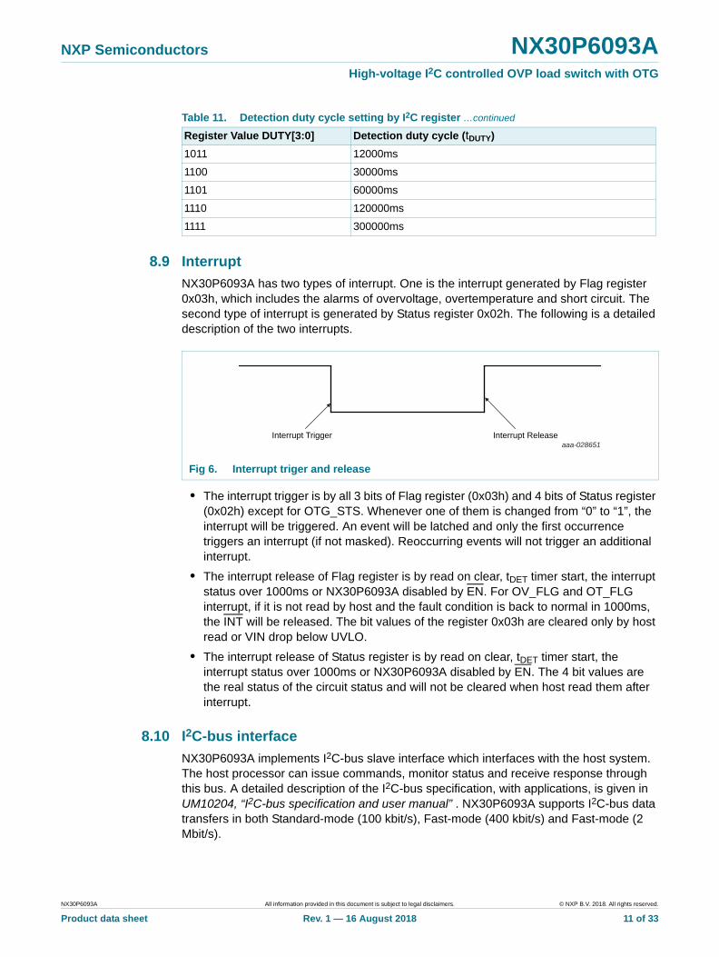
8.9 Interrupt
NX30P6093A has two types of interrupt. One is the interrupt generated by Flag register 0x03h, which includes the alarms of overvoltage, overtemperature and short circuit. The second type of interrupt is generated by Status register 0x02h. The following is a detailed description of the two interrupts.
• The interrupt trigger is by all 3 bits of Flag register (0x03h) and 4 bits of Status register (0x02h) except for OTG_STS. Whenever one of them is changed from “0” to “1”, the interrupt will be triggered. An event will be latched and only the first occurrence triggers an interrupt (if not masked). Reoccurring events will not trigger an additional interrupt.
• The interrupt release of Flag register is by read on clear, tDET timer start, the interrupt status over 1000ms or NX30P6093A disabled by EN. For OV_FLG and OT_FLG interrupt, if it is not read by host and the fault condition is back to normal in 1000ms, the INT will be released. The bit values of the register 0x03h are cleared only by host read or VIN drop below UVLO.
• The interrupt release of Status register is by read on clear, tDET timer start, the interrupt status over 1000ms or NX30P6093A disabled by EN. The 4 bit values are the real status of the circuit status and will not be cleared when host read them after interrupt.
8.10 I2C-bus interface
NX30P6093A implements I2C-bus slave interface which interfaces with the host system. The host processor can issue commands, monitor status and receive response through this bus. A detailed description of the I2C-bus specification, with applications, is given in UM10204, “I2C-bus specification and user manual” . NX30P6093A supports I2C-bus data transfers in both Standard-mode (100 kbit/s), Fast-mode (400 kbit/s) and Fast-mode (2 Mbit/s).
1011 12000ms
1100 30000ms
1101 60000ms
1110 120000ms
1111 300000ms
Table 11. Detection duty cycle setting by I2C register …continued
Register Value DUTY[3:0] Detection duty cycle (tDUTY)
Fig 6. Interrupt triger and release
aaa-028651Interrupt Trigger Interrupt Release
NX30P6093A All information provided in this document is subject to legal disclaimers. © NXP B.V. 2018. All rights reserved.
Product data sheet Rev. 1 — 16 August 2018 11 of 33
NXP Semiconductors NX30P6093AHigh-voltage I2C controlled OVP load switch with OTG
As an exception to the I2C-bus specification, the NX30P6093A does not support the I2C ‘General Call’ address (and therefore does not issue an Acknowledge), clock stretching, Software Reset command, nor 10-bit address.The various registers, address offsets and bit definitions are shown in Table 12.
The I2C address at Power-On Reset is as follows:
• Write address: 0x6C
• Read address: 0x6D
NX30P6093A All information provided in this document is subject to legal disclaimers. © NXP B.V. 2018. All rights reserved.
Product data sheet Rev. 1 — 16 August 2018 12 of 33
xxxxxxxxxxxxxxxxxxxxx xxxxxxxxxxxxxxxxxxxxxxxxxx xxxxxxx x x x xxxxxxxxxxxxxxxxxxxxxxxxxxxxxx xxxxxxxxxxxxxxxxxxx xx xx xxxxx xxxxxxxxxxxxxxxxxxxxxxxxxxx xxxxxxxxxxxxxxxxxxx xxxxxx xxxxxxxxxxxxxxxxxxxxxxxxxxxxxxxxxxx xxxxxxxxxxxx x x xxxxxxxxxxxxxxxxxxxxx xxxxxxxxxxxxxxxxxxxxxxxxxxxxxx xxxxx xxxxxxxxxxxxxxxxxxxxxxxxxxxxxxxxxxxxxxxxxxxxxxxxxx xxxxxxxx xxxxxxxxxxxxxxxxxxxxxxxxx xxxxxxxxxxxxxxxxxxxx xxx
NX
30P
6093A
All inform
ation provided
in this docum
ent is subject to leg
al disclaim
ers.©
NX
P B
.V. 2018. A
ll rights reserved.
Pro
du
ct data sh
eetR
ev. 1 — 16 A
ug
ust 2
018 13 o
f 33
NX
P S
emico
nd
ucto
rsN
X30P
6093AH
igh
-vo
ltage
I 2C c
on
trolle
d O
VP
loa
d s
witc
h w
ith O
TG
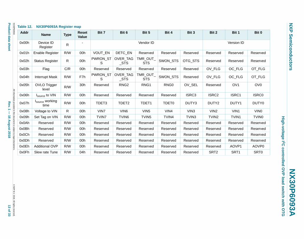
Table 12. NX30P6093A Register map
Bit 1 Bit 0
0 Version ID
0 Reserved Reserved
0 Reserved Reserved
0 OC_FLG OT_FLG
0 OC_FLG OT_FLG
0 OV1 OV0
0 ISRC1 ISRC0
0 DUTY1 DUTY0
0 VIN1 VIN0
0 TVIN1 TVIN0
0 Reserved Reserved
0 Reserved Reserved
0 Reserved Reserved
0 Reserved Reserved
0 AOVP1 AOVP0
0 SRT1 SRT0
AddrName Type
Reset Value
Bit 7 Bit 6 Bit 5 Bit 4 Bit 3 Bit 2
x00h Device ID Register
R- Vendor ID
x01h Enable Register R/W 00h VOUT_EN DETC_EN Reserved Reserved Reserved Reserved
x02h Status Register R 00hPWRON_ST
SOVER_TAG
_STSTMR_OUT_
STSSWON_STS OTG_STS Reserved
x03h Flag C/R 00h Reserved Reserved Reserved Reserved Reserved OV_FLG
x04h Interrupt Mask R/W F7hPWRON_ST
SOVER_TAG
_STSTMR_OUT_
STSSWON_STS Reserved OV_FLG
x05h OVLO Trigger level
R/W30h Reserved RNG2 RNG1 RNG0 OV_SEL Reserved
x06h Isource to VIN R/W 00h Reserved Reserved Reserved Reserved ISRC3 ISRC2
x07hIsource working
timeR/W 00h TDET3 TDET2 TDET1 TDET0 DUTY3 DUTY2
x08h Voltage to VIN R 00h VIN7 VIN6 VIN5 VIN4 VIN3 VIN2
x09h Set Tag on VIN R/W 00h TVIN7 TVIN6 TVIN5 TVIN4 TVIN3 TVIN2
x0Ah Reserved R/W 00h Reserved Reserved Reserved Reserved Reserved Reserved
x0Bh Reserved R/W 00h Reserved Reserved Reserved Reserved Reserved Reserved
x0Ch Reserved R/W 00h Reserved Reserved Reserved Reserved Reserved Reserved
x0Dh Reserved R/W 00h Reserved Reserved Reserved Reserved Reserved Reserved
x0Eh Additional OVP R/W 00h Reserved Reserved Reserved Reserved Reserved Reserved
x0Fh Slew rate Tune R/W 04h Reserved Reserved Reserved Reserved Reserved SRT2
NXP Semiconductors NX30P6093AHigh-voltage I2C controlled OVP load switch with OTG
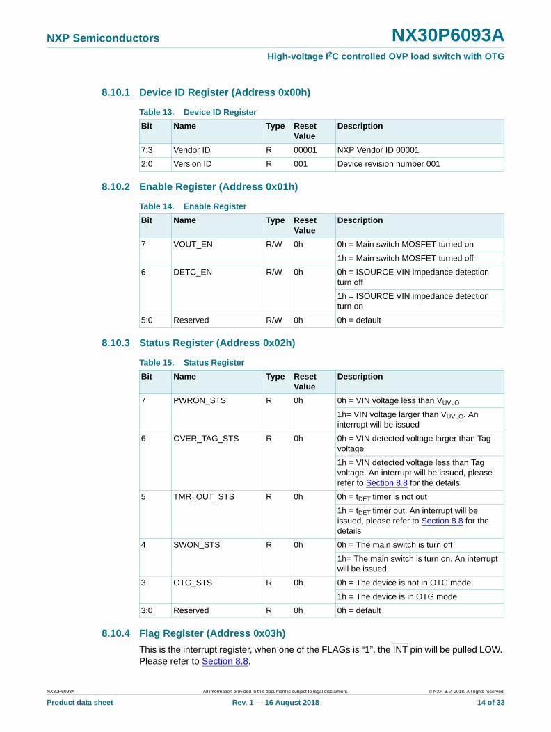
8.10.1 Device ID Register (Address 0x00h)
8.10.2 Enable Register (Address 0x01h)
8.10.3 Status Register (Address 0x02h)
8.10.4 Flag Register (Address 0x03h)
This is the interrupt register, when one of the FLAGs is “1”, the INT pin will be pulled LOW. Please refer to Section 8.8.
Table 13. Device ID Register
Bit Name Type Reset Value
Description
7:3 Vendor ID R 00001 NXP Vendor ID 00001
2:0 Version ID R 001 Device revision number 001
Table 14. Enable Register
Bit Name Type Reset Value
Description
7 VOUT_EN R/W 0h 0h = Main switch MOSFET turned on
1h = Main switch MOSFET turned off
6 DETC_EN R/W 0h 0h = ISOURCE VIN impedance detection turn off
1h = ISOURCE VIN impedance detection turn on
5:0 Reserved R/W 0h 0h = default
Table 15. Status Register
Bit Name Type Reset Value
Description
7 PWRON_STS R 0h 0h = VIN voltage less than VUVLO
1h= VIN voltage larger than VUVLO. An interrupt will be issued
6 OVER_TAG_STS R 0h 0h = VIN detected voltage larger than Tag voltage
1h = VIN detected voltage less than Tag voltage. An interrupt will be issued, please refer to Section 8.8 for the details
5 TMR_OUT_STS R 0h 0h = tDET timer is not out
1h = tDET timer out. An interrupt will be issued, please refer to Section 8.8 for the details
4 SWON_STS R 0h 0h = The main switch is turn off
1h= The main switch is turn on. An interrupt will be issued
3 OTG_STS R 0h 0h = The device is not in OTG mode
1h = The device is in OTG mode
3:0 Reserved R 0h 0h = default
NX30P6093A All information provided in this document is subject to legal disclaimers. © NXP B.V. 2018. All rights reserved.
Product data sheet Rev. 1 — 16 August 2018 14 of 33
NXP Semiconductors NX30P6093AHigh-voltage I2C controlled OVP load switch with OTG
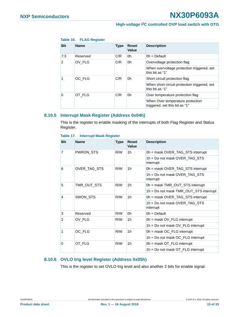
8.10.5 Interrupt Mask Register (Address 0x04h)
This is the register to enable masking of the interrupts of both Flag Register and Status Register.
8.10.6 OVLO trig level Register (Address 0x05h)
This is the register to set OVLO trig level and also another 2 bits for enable signal.
Table 16. FLAG Register
Bit Name Type Reset Value
Description
7:3 Reserved C/R 0h 0h = Default
2 OV_FLG C/R 0h Overvoltage protection flag
When overvoltage protection triggered, set this bit as “1”
1 OC_FLG C/R 0h Short circuit protection flag
When short circuit protection triggered, set this bit as “1”
0 OT_FLG C/R 0h Over temperature protection flag
When Over temperature protection triggered, set this bit as “1”
Table 17. Interrupt Mask Register
Bit Name Type Reset Value
Description
7 PWRON_STS R/W 1h 0h = mask OVER_TAG_STS interrupt
1h = Do not mask OVER_TAG_STS interrupt
6 OVER_TAG_STS R/W 1h 0h = mask OVER_TAG_STS interrupt
1h = Do not mask OVER_TAG_STS interrupt
5 TMR_OUT_STS R/W 1h 0h = mask TMR_OUT_STS interrupt
1h = Do not mask TMR_OUT_STS interrupt
4 SWON_STS R/W 1h 0h = mask OVER_TAG_STS interrupt
1h = Do not mask OVER_TAG_STS interrupt
3 Reserved R/W 0h 0h = Default
2 OV_FLG R/W 1h 0h = mask OV_FLG interrupt
1h = Do not mask OV_FLG interrupt
1 OC_FLG R/W 1h 0h = mask OC_FLG interrupt
1h = Do not mask OC_FLG interrupt
0 OT_FLG R/W 1h 0h = mask OT_FLG interrupt
1h = Do not mask OT_FLG interrupt
NX30P6093A All information provided in this document is subject to legal disclaimers. © NXP B.V. 2018. All rights reserved.
Product data sheet Rev. 1 — 16 August 2018 15 of 33
NXP Semiconductors NX30P6093AHigh-voltage I2C controlled OVP load switch with OTG
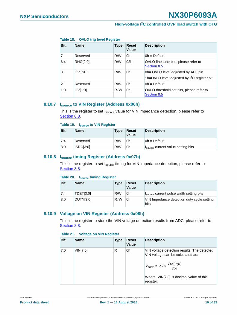
8.10.7 Isource to VIN Register (Address 0x06h)
This is the register to set Isource value for VIN impedance detection, please refer to Section 8.8.
8.10.8 Isource timing Register (Address 0x07h)
This is the register to set Isource timing for VIN impedance detection, please refer to Section 8.8.
8.10.9 Voltage on VIN Register (Address 0x08h)
This is the register to store the VIN voltage detection results from ADC, please refer to Section 8.8.
Table 18. OVLO trig level Register
Bit Name Type Reset Value
Description
7 Reserved R/W 0h 0h = Default
6:4 RNG[2:0] R/W 03h OVLO fine tune bits, please refer to Section 8.5
3 OV_SEL R/W 0h 0h= OVLO level adjusted by ADJ pin
1h=OVLO level adjusted by I2C register bit
2 Reserved R/W 0h 0h = Default
1:0 OV[1:0] R/W 0h OVLO threshold set bits, please refer to Section 8.5
Table 19. Isource to VIN Register
Bit Name Type Reset Value
Description
7:4 Reserved R/W 0h 0h = Default
3:0 ISRC[3:0] R/W 0h Isource current value setting bits
Table 20. Isource timing Register
Bit Name Type Reset Value
Description
7:4 TDET[3:0] R/W 0h Isource current pulse width setting bits
3:0 DUTY[3:0] R/W 0h VIN Impedance detection duty cycle setting bits
Table 21. Voltage on VIN Register
Bit Name Type Reset Value
Description
7:0 VIN[7:0] R 0h VIN voltage detection results. The detected VIN voltage can be calculated as:
Where, VIN[7:0] is decimal value of this register.
VDET 2.7VIN 7 0;
256-----------------------=
NX30P6093A All information provided in this document is subject to legal disclaimers. © NXP B.V. 2018. All rights reserved.
Product data sheet Rev. 1 — 16 August 2018 16 of 33
NXP Semiconductors NX30P6093AHigh-voltage I2C controlled OVP load switch with OTG
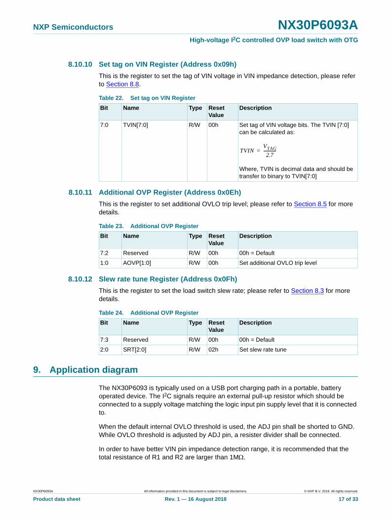
8.10.10 Set tag on VIN Register (Address 0x09h)
This is the register to set the tag of VIN voltage in VIN impedance detection, please refer to Section 8.8.
8.10.11 Additional OVP Register (Address 0x0Eh)
This is the register to set additional OVLO trip level; please refer to Section 8.5 for more details.
8.10.12 Slew rate tune Register (Address 0x0Fh)
This is the register to set the load switch slew rate; please refer to Section 8.3 for more details.
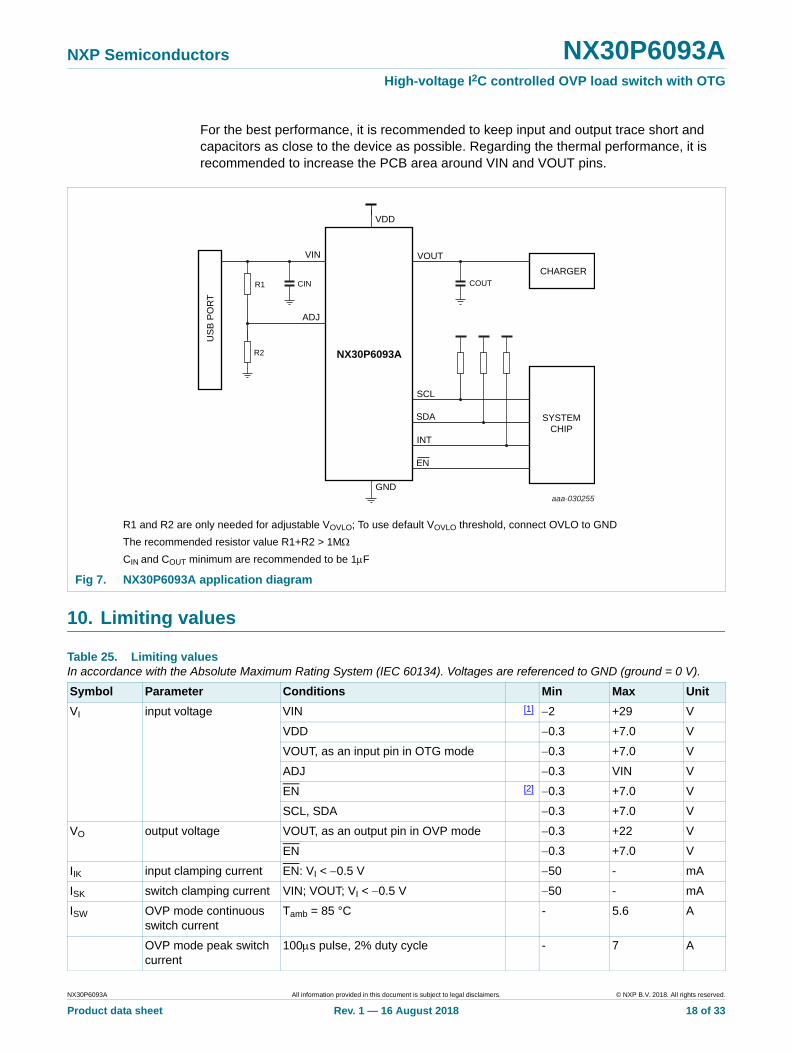
9. Application diagram
The NX30P6093 is typically used on a USB port charging path in a portable, battery operated device. The I2C signals require an external pull-up resistor which should be connected to a supply voltage matching the logic input pin supply level that it is connected to.
When the default internal OVLO threshold is used, the ADJ pin shall be shorted to GND. While OVLO threshold is adjusted by ADJ pin, a resister divider shall be connected.
In order to have better VIN pin impedance detection range, it is recommended that the total resistance of R1 and R2 are larger than 1M.
Table 22. Set tag on VIN Register
Bit Name Type Reset Value
Description
7:0 TVIN[7:0] R/W 00h Set tag of VIN voltage bits. The TVIN [7:0] can be calculated as:
Where, TVIN is decimal data and should be transfer to binary to TVIN[7:0]
TVINVTAG
2.7-------------=
Table 23. Additional OVP Register
Bit Name Type Reset Value
Description
7:2 Reserved R/W 00h 00h = Default
1:0 AOVP[1:0] R/W 00h Set additional OVLO trip level
Table 24. Additional OVP Register
Bit Name Type Reset Value
Description
7:3 Reserved R/W 00h 00h = Default
2:0 SRT[2:0] R/W 02h Set slew rate tune
NX30P6093A All information provided in this document is subject to legal disclaimers. © NXP B.V. 2018. All rights reserved.
Product data sheet Rev. 1 — 16 August 2018 17 of 33
NXP Semiconductors NX30P6093AHigh-voltage I2C controlled OVP load switch with OTG
For the best performance, it is recommended to keep input and output trace short and capacitors as close to the device as possible. Regarding the thermal performance, it is recommended to increase the PCB area around VIN and VOUT pins.
10. Limiting values
R1 and R2 are only needed for adjustable VOVLO; To use default VOVLO threshold, connect OVLO to GND
The recommended resistor value R1+R2 > 1M
CIN and COUT minimum are recommended to be 1F
Fig 7. NX30P6093A application diagram
aaa-030255
US
B P
OR
T
SYSTEMCHIP
CHARGERVOUT
SCL
SDA
INT
VIN
CIN COUT
ADJ
EN
GND
VDD
NX30P6093A
R1
R2
Table 25. Limiting valuesIn accordance with the Absolute Maximum Rating System (IEC 60134). Voltages are referenced to GND (ground = 0 V).
Symbol Parameter Conditions Min Max Unit
VI input voltage VIN [1] 2 +29 V
VDD 0.3 +7.0 V
VOUT, as an input pin in OTG mode 0.3 +7.0 V
ADJ 0.3 VIN V
EN [2] 0.3 +7.0 V
SCL, SDA 0.3 +7.0 V
VO output voltage VOUT, as an output pin in OVP mode 0.3 +22 V
EN 0.3 +7.0 V
IIK input clamping current EN: VI < 0.5 V 50 - mA
ISK switch clamping current VIN; VOUT; VI < 0.5 V 50 - mA
ISW OVP mode continuous switch current
Tamb = 85 °C - 5.6 A
OVP mode peak switch current
100s pulse, 2% duty cycle - 7 A
NX30P6093A All information provided in this document is subject to legal disclaimers. © NXP B.V. 2018. All rights reserved.
Product data sheet Rev. 1 — 16 August 2018 18 of 33
NXP Semiconductors NX30P6093AHigh-voltage I2C controlled OVP load switch with OTG
[1] The -2V limiting value is 200ms non-repetitive pulse
[2] The minimum input voltage rating may be exceeded if the input current rating is observed.
[3] The (absolute) maximum power dissipation depends on the junction temperature Tj. Higher power dissipation is allowed in conjunction with lower ambient temperatures. The conditions to determine the specified values are Tamb = 25 C and the use of a 4 layer PCB.
11. Recommended operating conditions
12. Thermal characteristics
[1] The overall Rth(j-a) can vary depending on the board layout. To minimize the effective Rth(j-a), all pins must have a solid connection to larger Cu layer areas e.g. to the power and ground layer. In multi-layer PCB applications, the second layer should be used to create a large heat spreader area right below the device. If this layer is either ground or power, it should be connected with several vias to the top layer connecting to the device ground or supply. Try not to use any solder-stop varnish under the chip.
[2] Rth(j-a) is calculated based on JEDEX2S2P board. The actual Rth(j-a) value may vary in applications using different layer stacks and layouts.
OTG mode continuous switch current
Tamb = 85 °C - 1.5 A
Tstg storage temperature 65 +150 C
Ptot total power dissipation [3] - 1.7 W
Table 25. Limiting values …continuedIn accordance with the Absolute Maximum Rating System (IEC 60134). Voltages are referenced to GND (ground = 0 V).
Symbol Parameter Conditions Min Max Unit
Table 26. Recommended operating conditions
Symbol Parameter Conditions Min Max Unit
VI input voltage VIN 0 20 V
VOUT (OTG Mode input voltage) 4.5 5.5 V
EN 0 5.5 V
VDD 3.0 4.5 V
VO output voltage INT 0 5.5 V
Tj(max) maximum junction temperature 40 +125 C
Tamb ambient temperature 40 +85 C
Table 27. Thermal characteristics
Symbol Parameter Conditions Typ Unit
Rth(j-a) thermal resistance from junction to ambient [1][2] 58.6 K/W
NX30P6093A All information provided in this document is subject to legal disclaimers. © NXP B.V. 2018. All rights reserved.
Product data sheet Rev. 1 — 16 August 2018 19 of 33
NXP Semiconductors NX30P6093AHigh-voltage I2C controlled OVP load switch with OTG
13. Static characteristics
Table 28. Static characteristicsAt recommended operating conditions; voltages are referenced to GND (ground = 0 V).
Symbol Parameter Conditions Tamb = 25 C Tamb = 40 C to +85 C Unit
Min Typ Max Min Max
VIH HIGH-level input voltage
EN pin; VI(VIN) = 2.8V to 20V
1.2 - - 1.2 - V
VIL LOW-level input voltage
EN pin; VI(VIN) = 2.8V to 20V
- - 0.4 - 0.4 V
IEN Input leakage current
EN pin; VI(EN)=0V - 0.1 - -1 1 A
CI input capacitance EN pin; VI(VIN) = 5V - 5 - - - pF
Rpd pull-down resistance EN pin; - 1 - - - M
Iq VIN quiescent current
EN = 0 V; VI(VIN) = 5.0 V; IO = 0 A;
- 150 - - 200 A
EN = 5.0 V; VI(VIN) = 5.0 V; IO = 0 A;
- 1 - - 3 A
Iq_SLEEP VDD Sleep mode current
EN = 0 V; VI(VIN) <VUVLO; VDD=3.0V; DETC_EN=0
- 12.5 - - 20.5 A
Iq_OTG VOUT quiescent current
EN = 0 V; VI(VOUT) = 5.0 V; IO = 0 A;
- 160 - - 210 A
IDET_LEAKAGE VIN Pin leakage in detection mode
EN = 0 V; VI(VIN) =1V; DETC_EN=1
- 0.2 - - 0.5 A
IS(OFF) VOUT OFF-state leakage current
EN = 5.0 V; VI(VIN) = 5.0V; VOUT = 0 V
- 0.5 - - 2 A
VUVLO undervoltage lockout release voltage
VIN Rising; EN = 0 V - 2.65 - 2.5 2.8 V
Vhys(UVLO) undervoltage lockout hysteresis voltage
VIN Falling; - 100 - mV
IOVLO ADJ pin input leakage Current
VIN=5V, VADJ=3V apply after power up
- 3 - - 6 A
VIN=5V, VADJ=3V apply before power up
- 10 - - 100 nA
VOVLO Default overvoltage lockout voltage
VIN Rising; EN = 0 V; ADJ short to GND
- 6.8 - 6.6 7.0 V
Vhys(OVLO) Overvoltage lockout hysteresis voltage
VIN Falling; EN = 0 V; ADJ short to GND
- 2 - 1.3 2.7 %
Vth(OVLO) external OVLO set threshold voltage
VI(VIN) = 2.8V to 20V; EN = 0 V
- 1.204 - 1.175 1.224 V
I2C-bus Interface Specifications
VIH HIGH-level input voltage
SCL, SDA; VDD= 3.0V to 4.5V
1.2 - - 1.2 - V
VIL LOW-level input voltage
SCL, SDA; VDD= 3.0V to 4.5V
- - 0.4 - 0.4 V
VOL LOW-level output voltage
INT pin; VDD= 3.0V to 4.5V; Iload = 1mA
- - 0.3 - 0.3 V
NX30P6093A All information provided in this document is subject to legal disclaimers. © NXP B.V. 2018. All rights reserved.
Product data sheet Rev. 1 — 16 August 2018 20 of 33
NXP Semiconductors NX30P6093AHigh-voltage I2C controlled OVP load switch with OTG
fCLK_I2C I2C-bus clock frequency
0 - 1 0 1 MHz
ISOURCE ADC Specifications
ISOURCE_ACC Current source accuracy
VDD= 3.0V to 4.5V - - 5 - 5 %
VADC ADC input voltage range
VDD= 3.0V to 4.5V 0 2.5 0 2.5 V
VADC ADC reference voltage
VDD= 3.0V to 4.5V - 2.7 - 2.64 2.76 V
Resolution ADC bits VDD= 3.0V to 4.5V - 8 - - - bit
Thermal Protection
Tth(otp) over temperature shutdown threshold temperature
VIN=2.8V to 20V - 140 - - - C
Tth(otp)hys hysteresis of over temperature protection threshold temperature
VIN=2.8V to 20V - 25 - - - C
Table 28. Static characteristics …continuedAt recommended operating conditions; voltages are referenced to GND (ground = 0 V).
Symbol Parameter Conditions Tamb = 25 C Tamb = 40 C to +85 C Unit
Min Typ Max Min Max
NX30P6093A All information provided in this document is subject to legal disclaimers. © NXP B.V. 2018. All rights reserved.
Product data sheet Rev. 1 — 16 August 2018 21 of 33
NXP Semiconductors NX30P6093AHigh-voltage I2C controlled OVP load switch with OTG
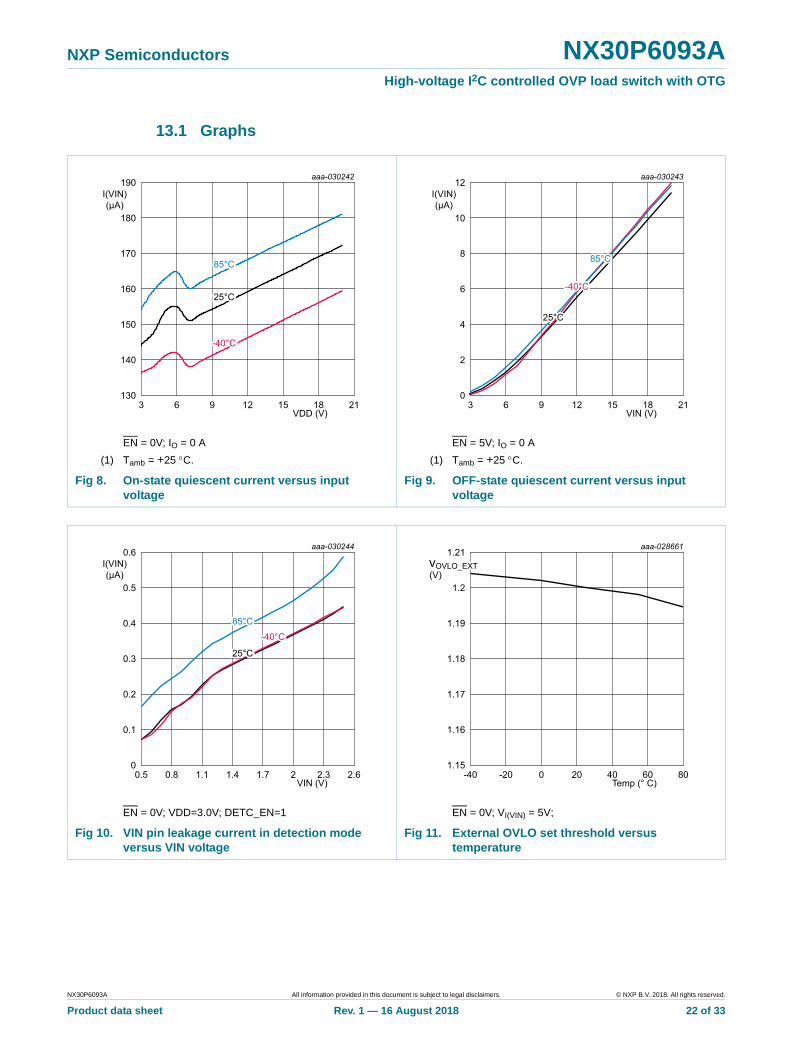
13.1 Graphs
EN = 0V; IO = 0 A
(1) Tamb = +25 C.
EN = 5V; IO = 0 A
(1) Tamb = +25 C.
Fig 8. On-state quiescent current versus input voltage
Fig 9. OFF-state quiescent current versus input voltage
EN = 0V; VDD=3.0V; DETC_EN=1 EN = 0V; VI(VIN) = 5V;
Fig 10. VIN pin leakage current in detection mode versus VIN voltage
Fig 11. External OVLO set threshold versus temperature
NX30P6093A All information provided in this document is subject to legal disclaimers. © NXP B.V. 2018. All rights reserved.
Product data sheet Rev. 1 — 16 August 2018 22 of 33
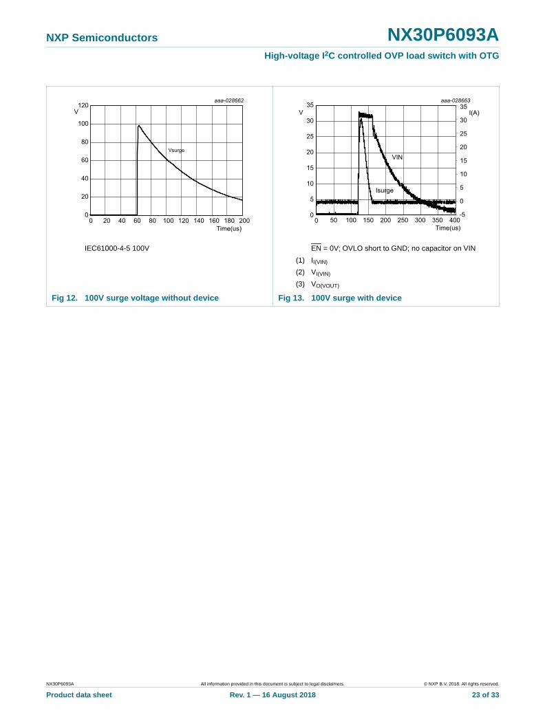
NXP Semiconductors NX30P6093AHigh-voltage I2C controlled OVP load switch with OTG
IEC61000-4-5 100V EN = 0V; OVLO short to GND; no capacitor on VIN
(1) II(VIN)
(2) VI(VIN)
(3) VO(VOUT)
Fig 12. 100V surge voltage without device Fig 13. 100V surge with device
NX30P6093A All information provided in this document is subject to legal disclaimers. © NXP B.V. 2018. All rights reserved.
Product data sheet Rev. 1 — 16 August 2018 23 of 33
NXP Semiconductors NX30P6093AHigh-voltage I2C controlled OVP load switch with OTG
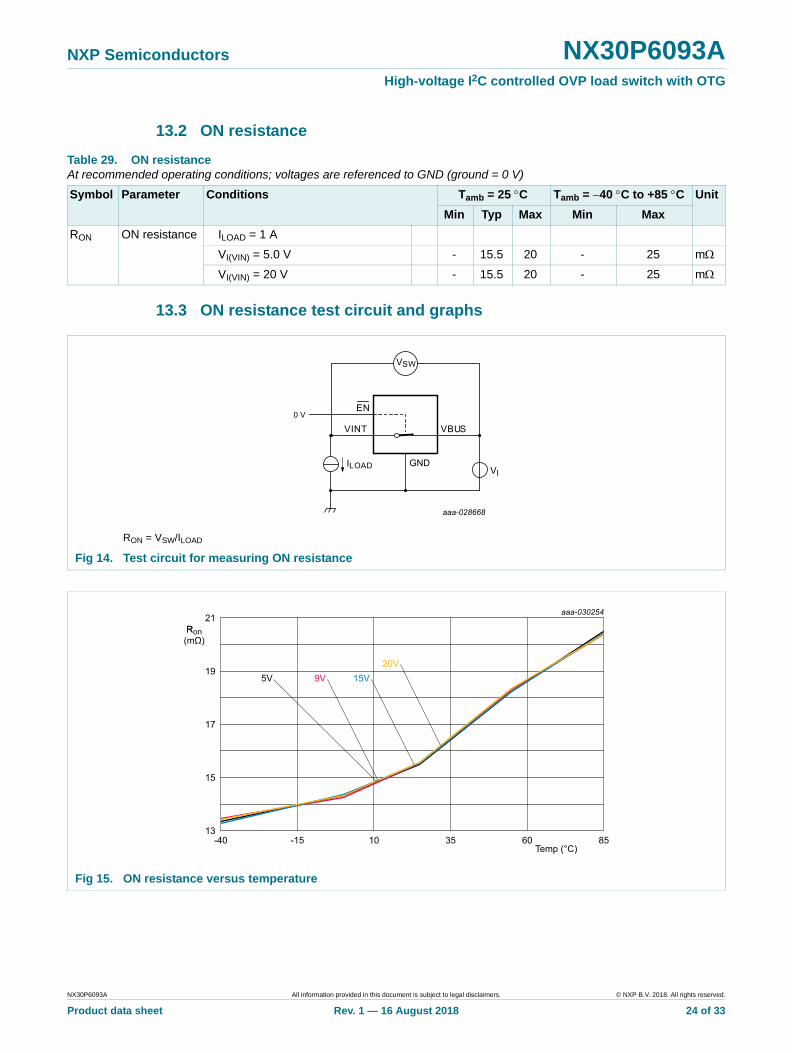
13.2 ON resistance
13.3 ON resistance test circuit and graphs
Table 29. ON resistanceAt recommended operating conditions; voltages are referenced to GND (ground = 0 V)
Symbol Parameter Conditions Tamb = 25 C Tamb = 40 C to +85 C Unit
Min Typ Max Min Max
RON ON resistance ILOAD = 1 A
VI(VIN) = 5.0 V - 15.5 20 - 25 m
VI(VIN) = 20 V - 15.5 20 - 25 m
RON = VSW/ILOAD
Fig 14. Test circuit for measuring ON resistance
Fig 15. ON resistance versus temperature
NX30P6093A All information provided in this document is subject to legal disclaimers. © NXP B.V. 2018. All rights reserved.
Product data sheet Rev. 1 — 16 August 2018 24 of 33
NXP Semiconductors NX30P6093AHigh-voltage I2C controlled OVP load switch with OTG
14. Dynamic characteristics
[1] Guaranteed by design
Table 30. Dynamic characteristicsAt recommended operating conditions; voltages are referenced to GND (ground = 0 V); for test circuit see Figure 17.
Symbol Parameter Conditions Tamb = 25 C Tamb = 40 C to +85 C Unit
Min Typ Max Min Max
ten Enable Time From EN to V(VOUT) = 10 % of V(VIN); (Including debounce time); VI(VIN) = 5 V; CLoad = 22 F; RLoad = 100
- 15 - 10 20 ms
tTLH VOUT rise time
V(VOUT) from 10 % to 90 % V(VIN); CLoad = 22 F; RLoad = 100
VI(VIN) = 5 V - 0.9 - - 2 ms
VI(VIN) = 20 V - 1.8 - - 3 ms
tdis(OVP) OVLO turn off time
From V(VIN)>VOVLO to V(VOUT) = 80 % of V(VIN); Rload = 100 ,; Cload = 0 F; VI(VIN) = 20 V; ADJ pin short to GND; VIN rise >2 V/us
- 30 - - 100 ns
tstart VIN start time EN = 0; from VIN > VUVLO to V(VOUT) = 10 % of V(VIN)
- 15 - 10 20 ms
tdis Disable time From EN to V(VOUT) = 90 % of V(VIN); VI(VIN) = 5 V; CLoad = 0 F; RLoad = 100
- 0.2 - 0.1 0.5 s
tDEB Debounce time
Time from VUVLO < VIN < VOVLO to V(VOUT) = 10 % of V(VIN)
- 13.5 - - - ms
tWAKEUP[1] Sleep to VIN
detection wake up time
Time from DETC_EN = 1 to device ready for VIN impedance detection
- 1.5 3 - 3 ms
tSCP Short circuit protection response time
VIN=5 V; Time from short circuit happened to switch turn off
- 3 - - - s
tVINDISCHARGE Time taken for VIN discharge
VDD = 3.3 V;
Load Capacitance = 10 F VBUS pin going down below Vsafe0V after VBUS detached and switch disabled
- - - - 650 ms
VDD = 3.3 V;
Load Capacitance = 10 F
VBUS pin going down below
Vsafe5V (when initial voltage is >5 V) after VBUS detached and switch disabled
- - - - 275 ms
NX30P6093A All information provided in this document is subject to legal disclaimers. © NXP B.V. 2018. All rights reserved.
Product data sheet Rev. 1 — 16 August 2018 25 of 33
NXP Semiconductors NX30P6093AHigh-voltage I2C controlled OVP load switch with OTG
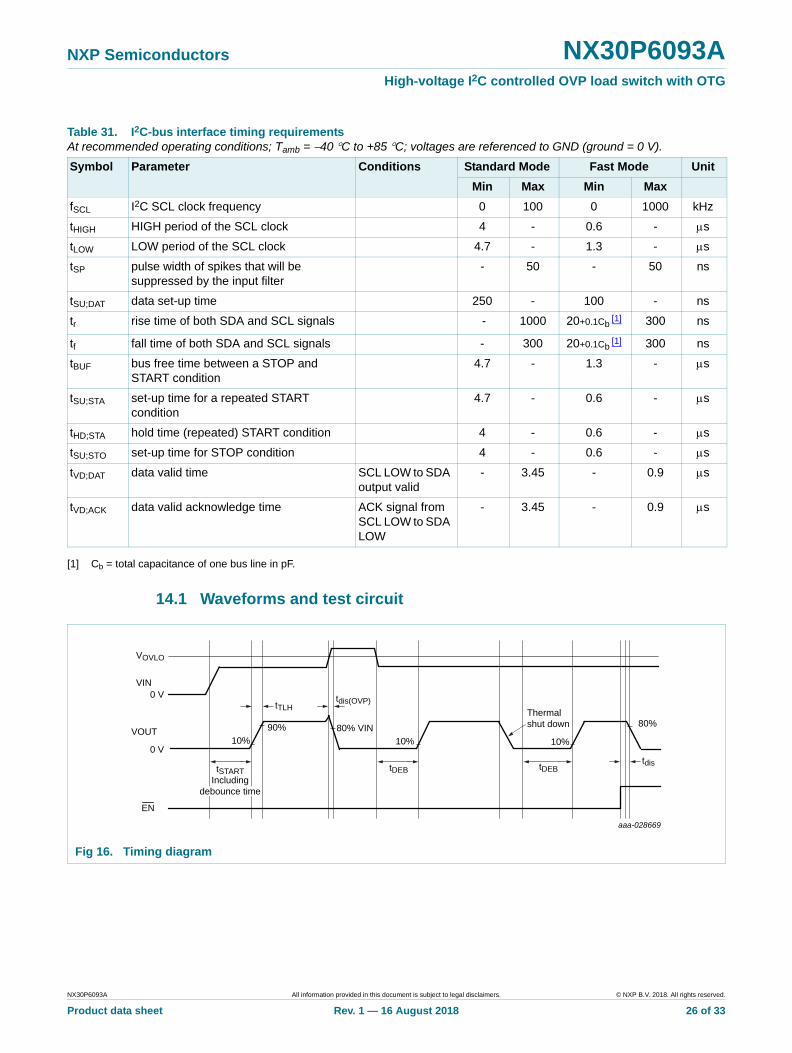
[1] Cb = total capacitance of one bus line in pF.
14.1 Waveforms and test circuit
Table 31. I2C-bus interface timing requirementsAt recommended operating conditions; Tamb = 40 C to +85 C; voltages are referenced to GND (ground = 0 V).
Symbol Parameter Conditions Standard Mode Fast Mode Unit
Min Max Min Max
fSCL I2C SCL clock frequency 0 100 0 1000 kHz
tHIGH HIGH period of the SCL clock 4 - 0.6 - s
tLOW LOW period of the SCL clock 4.7 - 1.3 - s
tSP pulse width of spikes that will be suppressed by the input filter
- 50 - 50 ns
tSU;DAT data set-up time 250 - 100 - ns
tr rise time of both SDA and SCL signals - 1000 20+0.1Cb [1] 300 ns
tf fall time of both SDA and SCL signals - 300 20+0.1Cb [1] 300 ns
tBUF bus free time between a STOP and START condition
4.7 - 1.3 - s
tSU;STA set-up time for a repeated START condition
4.7 - 0.6 - s
tHD;STA hold time (repeated) START condition 4 - 0.6 - s
tSU;STO set-up time for STOP condition 4 - 0.6 - s
tVD;DAT data valid time SCL LOW to SDA output valid
- 3.45 - 0.9 s
tVD;ACK data valid acknowledge time ACK signal from SCL LOW to SDA LOW
- 3.45 - 0.9 s
Fig 16. Timing diagram
VIN
VOUT
tTLH
tDEB
VOVLO
0 V
0 V
EN
tDEBtdis
tdis(OVP)
80% VIN10%
Thermal shut down90%
10%
80%
aaa-028669
10%
tSTARTIncluding
debounce time
NX30P6093A All information provided in this document is subject to legal disclaimers. © NXP B.V. 2018. All rights reserved.
Product data sheet Rev. 1 — 16 August 2018 26 of 33
NXP Semiconductors NX30P6093AHigh-voltage I2C controlled OVP load switch with OTG
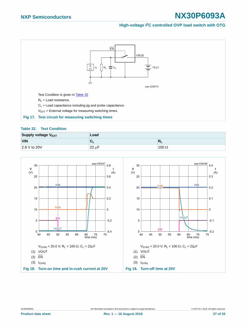
Test Condition is given in Table 32
RL = Load resistance.
CL = Load capacitance including jig and probe capacitance.
VEXT = External voltage for measuring switching times.
Fig 17. Test circuit for measuring switching times
aaa-028670
Table 32. Test Condition
Supply voltage VEXT Load
VIN CL RL
2.8 V to 20V 22 F 100
VI(VIN) = 20.0 V; RL = 100 ; CL = 22F
(1) VOUT
(2) EN
(3) II(VIN)
VI(VIN) = 20.0 V; RL = 100 ; CL = 22F
(1) VOUT
(2) EN
(3) II(VIN)
Fig 18. Turn-on time and in-rush current at 20V Fig 19. Turn-off time at 20V
NX30P6093A All information provided in this document is subject to legal disclaimers. © NXP B.V. 2018. All rights reserved.
Product data sheet Rev. 1 — 16 August 2018 27 of 33
NXP Semiconductors NX30P6093AHigh-voltage I2C controlled OVP load switch with OTG
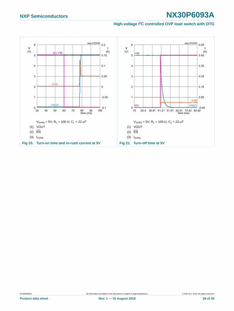
VI(VIN) = 5V; RL = 100 ; CL = 22 F
(1) VOUT
(2) EN
(3) II(VIN)
VI(VIN) = 5V; RL = 100 ; CL = 22 F
(1) VOUT
(2) EN
(3) II(VIN)
Fig 20. Turn-on time and in-rush current at 5V Fig 21. Turn-off time at 5V
NX30P6093A All information provided in this document is subject to legal disclaimers. © NXP B.V. 2018. All rights reserved.
Product data sheet Rev. 1 — 16 August 2018 28 of 33
NXP Semiconductors NX30P6093AHigh-voltage I2C controlled OVP load switch with OTG
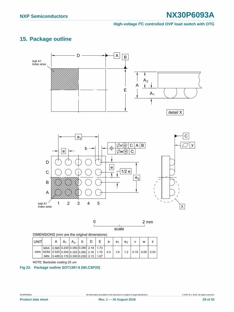
15. Package outline
Fig 22. Package outline SOT1397-6 (WLCSP20)
NX30P6093A All information provided in this document is subject to legal disclaimers. © NXP B.V. 2018. All rights reserved.
Product data sheet Rev. 1 — 16 August 2018 29 of 33
NXP Semiconductors NX30P6093AHigh-voltage I2C controlled OVP load switch with OTG
16. Revision history
Document ID Release date Data sheet status Change notice Supersedes
NX30P6093A v.1 20180816 Product data sheet - -
NX30P6093A All information provided in this document is subject to legal disclaimers. © NXP B.V. 2018. All rights reserved.
Product data sheet Rev. 1 — 16 August 2018 30 of 33
NXP Semiconductors NX30P6093AHigh-voltage I2C controlled OVP load switch with OTG
17. Legal information
17.1 Data sheet status
[1] Please consult the most recently issued document before initiating or completing a design.
[2] The term ‘short data sheet’ is explained in section “Definitions”.
[3] The product status of device(s) described in this document may have changed since this document was published and may differ in case of multiple devices. The latest product status information is available on the Internet at URL http://www.nxp.com.
17.2 Definitions
Draft — The document is a draft version only. The content is still under internal review and subject to formal approval, which may result in modifications or additions. NXP Semiconductors does not give any representations or warranties as to the accuracy or completeness of information included herein and shall have no liability for the consequences of use of such information.
Short data sheet — A short data sheet is an extract from a full data sheet with the same product type number(s) and title. A short data sheet is intended for quick reference only and should not be relied upon to contain detailed and full information. For detailed and full information see the relevant full data sheet, which is available on request via the local NXP Semiconductors sales office. In case of any inconsistency or conflict with the short data sheet, the full data sheet shall prevail.
Product specification — The information and data provided in a Product data sheet shall define the specification of the product as agreed between NXP Semiconductors and its customer, unless NXP Semiconductors and customer have explicitly agreed otherwise in writing. In no event however, shall an agreement be valid in which the NXP Semiconductors product is deemed to offer functions and qualities beyond those described in the Product data sheet.
17.3 Disclaimers
Limited warranty and liability — Information in this document is believed to be accurate and reliable. However, NXP Semiconductors does not give any representations or warranties, expressed or implied, as to the accuracy or completeness of such information and shall have no liability for the consequences of use of such information. NXP Semiconductors takes no responsibility for the content in this document if provided by an information source outside of NXP Semiconductors.
In no event shall NXP Semiconductors be liable for any indirect, incidental, punitive, special or consequential damages (including - without limitation - lost profits, lost savings, business interruption, costs related to the removal or replacement of any products or rework charges) whether or not such damages are based on tort (including negligence), warranty, breach of contract or any other legal theory.
Notwithstanding any damages that customer might incur for any reason whatsoever, NXP Semiconductors’ aggregate and cumulative liability towards customer for the products described herein shall be limited in accordance with the Terms and conditions of commercial sale of NXP Semiconductors.
Right to make changes — NXP Semiconductors reserves the right to make changes to information published in this document, including without limitation specifications and product descriptions, at any time and without notice. This document supersedes and replaces all information supplied prior to the publication hereof.
Suitability for use — NXP Semiconductors products are not designed, authorized or warranted to be suitable for use in life support, life-critical or safety-critical systems or equipment, nor in applications where failure or malfunction of an NXP Semiconductors product can reasonably be expected to result in personal injury, death or severe property or environmental damage. NXP Semiconductors and its suppliers accept no liability for inclusion and/or use of NXP Semiconductors products in such equipment or applications and therefore such inclusion and/or use is at the customer’s own risk.
Applications — Applications that are described herein for any of these products are for illustrative purposes only. NXP Semiconductors makes no representation or warranty that such applications will be suitable for the specified use without further testing or modification.
Customers are responsible for the design and operation of their applications and products using NXP Semiconductors products, and NXP Semiconductors accepts no liability for any assistance with applications or customer product design. It is customer’s sole responsibility to determine whether the NXP Semiconductors product is suitable and fit for the customer’s applications and products planned, as well as for the planned application and use of customer’s third party customer(s). Customers should provide appropriate design and operating safeguards to minimize the risks associated with their applications and products.
NXP Semiconductors does not accept any liability related to any default, damage, costs or problem which is based on any weakness or default in the customer’s applications or products, or the application or use by customer’s third party customer(s). Customer is responsible for doing all necessary testing for the customer’s applications and products using NXP Semiconductors products in order to avoid a default of the applications and the products or of the application or use by customer’s third party customer(s). NXP does not accept any liability in this respect.
Limiting values — Stress above one or more limiting values (as defined in the Absolute Maximum Ratings System of IEC 60134) will cause permanent damage to the device. Limiting values are stress ratings only and (proper) operation of the device at these or any other conditions above those given in the Recommended operating conditions section (if present) or the Characteristics sections of this document is not warranted. Constant or repeated exposure to limiting values will permanently and irreversibly affect the quality and reliability of the device.
Terms and conditions of commercial sale — NXP Semiconductors products are sold subject to the general terms and conditions of commercial sale, as published at http://www.nxp.com/profile/terms, unless otherwise agreed in a valid written individual agreement. In case an individual agreement is concluded only the terms and conditions of the respective agreement shall apply. NXP Semiconductors hereby expressly objects to applying the customer’s general terms and conditions with regard to the purchase of NXP Semiconductors products by customer.
No offer to sell or license — Nothing in this document may be interpreted or construed as an offer to sell products that is open for acceptance or the grant, conveyance or implication of any license under any copyrights, patents or other industrial or intellectual property rights.
Document status[1][2] Product status[3] Definition
Objective [short] data sheet Development This document contains data from the objective specification for product development.
Preliminary [short] data sheet Qualification This document contains data from the preliminary specification.
Product [short] data sheet Production This document contains the product specification.
NX30P6093A All information provided in this document is subject to legal disclaimers. © NXP B.V. 2018. All rights reserved.
Product data sheet Rev. 1 — 16 August 2018 31 of 33
NXP Semiconductors NX30P6093AHigh-voltage I2C controlled OVP load switch with OTG
Export control — This document as well as the item(s) described herein may be subject to export control regulations. Export might require a prior authorization from competent authorities.
Non-automotive qualified products — Unless this data sheet expressly states that this specific NXP Semiconductors product is automotive qualified, the product is not suitable for automotive use. It is neither qualified nor tested in accordance with automotive testing or application requirements. NXP Semiconductors accepts no liability for inclusion and/or use of non-automotive qualified products in automotive equipment or applications.
In the event that customer uses the product for design-in and use in automotive applications to automotive specifications and standards, customer (a) shall use the product without NXP Semiconductors’ warranty of the product for such automotive applications, use and specifications, and (b) whenever customer uses the product for automotive applications beyond
NXP Semiconductors’ specifications such use shall be solely at customer’s own risk, and (c) customer fully indemnifies NXP Semiconductors for any liability, damages or failed product claims resulting from customer design and use of the product for automotive applications beyond NXP Semiconductors’ standard warranty and NXP Semiconductors’ product specifications.
Translations — A non-English (translated) version of a document is for reference only. The English version shall prevail in case of any discrepancy between the translated and English versions.
17.4 TrademarksNotice: All referenced brands, product names, service names and trademarks are the property of their respective owners.
18. Contact information
For more information, please visit: http://www.nxp.com
For sales office addresses, please send an email to: [email protected]
NX30P6093A All information provided in this document is subject to legal disclaimers. © NXP B.V. 2018. All rights reserved.
Product data sheet Rev. 1 — 16 August 2018 32 of 33
NXP Semiconductors NX30P6093AHigh-voltage I2C controlled OVP load switch with OTG
19. Contents
1 General description . . . . . . . . . . . . . . . . . . . . . . 1
2 Features and benefits . . . . . . . . . . . . . . . . . . . . 1
3 Applications . . . . . . . . . . . . . . . . . . . . . . . . . . . . 2
4 Ordering information. . . . . . . . . . . . . . . . . . . . . 24.1 Ordering options . . . . . . . . . . . . . . . . . . . . . . . . 2
5 Marking . . . . . . . . . . . . . . . . . . . . . . . . . . . . . . . . 2
6 Functional diagram . . . . . . . . . . . . . . . . . . . . . . 3
7 Pinning information. . . . . . . . . . . . . . . . . . . . . . 47.1 Pinning . . . . . . . . . . . . . . . . . . . . . . . . . . . . . . . 47.2 Pin description . . . . . . . . . . . . . . . . . . . . . . . . . 4
8 Functional description . . . . . . . . . . . . . . . . . . . 58.1 EN input . . . . . . . . . . . . . . . . . . . . . . . . . . . . . . 58.2 OTG Mode . . . . . . . . . . . . . . . . . . . . . . . . . . . . 58.3 Slew Rate Tune . . . . . . . . . . . . . . . . . . . . . . . . 58.4 Undervoltage lockout . . . . . . . . . . . . . . . . . . . . 68.5 Overvoltage lockout . . . . . . . . . . . . . . . . . . . . . 68.6 Overtemperature protection . . . . . . . . . . . . . . . 88.7 Short circuit protection . . . . . . . . . . . . . . . . . . . 88.8 VIN impedance detection . . . . . . . . . . . . . . . . . 88.9 Interrupt . . . . . . . . . . . . . . . . . . . . . . . . . . . . . 118.10 I2C-bus interface. . . . . . . . . . . . . . . . . . . . . . . 118.10.1 Device ID Register (Address 0x00h) . . . . . . . 148.10.2 Enable Register (Address 0x01h). . . . . . . . . . 148.10.3 Status Register (Address 0x02h) . . . . . . . . . . 148.10.4 Flag Register (Address 0x03h). . . . . . . . . . . . 148.10.5 Interrupt Mask Register (Address 0x04h). . . . 158.10.6 OVLO trig level Register (Address 0x05h) . . . 158.10.7 Isource to VIN Register (Address 0x06h) . . . . . 168.10.8 Isource timing Register (Address 0x07h) . . . . . 168.10.9 Voltage on VIN Register (Address 0x08h) . . . 168.10.10 Set tag on VIN Register (Address 0x09h). . . . 178.10.11 Additional OVP Register (Address 0x0Eh) . . . 178.10.12 Slew rate tune Register (Address 0x0Fh). . . . 17
9 Application diagram . . . . . . . . . . . . . . . . . . . . 17
10 Limiting values. . . . . . . . . . . . . . . . . . . . . . . . . 18
11 Recommended operating conditions. . . . . . . 19
12 Thermal characteristics . . . . . . . . . . . . . . . . . 19
13 Static characteristics. . . . . . . . . . . . . . . . . . . . 2013.1 Graphs . . . . . . . . . . . . . . . . . . . . . . . . . . . . . . 2213.2 ON resistance. . . . . . . . . . . . . . . . . . . . . . . . . 2413.3 ON resistance test circuit and graphs. . . . . . . 24
14 Dynamic characteristics . . . . . . . . . . . . . . . . . 2514.1 Waveforms and test circuit . . . . . . . . . . . . . . . 26
15 Package outline . . . . . . . . . . . . . . . . . . . . . . . . 29
16 Revision history. . . . . . . . . . . . . . . . . . . . . . . . 30
17 Legal information . . . . . . . . . . . . . . . . . . . . . . 3117.1 Data sheet status . . . . . . . . . . . . . . . . . . . . . . 3117.2 Definitions . . . . . . . . . . . . . . . . . . . . . . . . . . . 3117.3 Disclaimers . . . . . . . . . . . . . . . . . . . . . . . . . . 3117.4 Trademarks . . . . . . . . . . . . . . . . . . . . . . . . . . 32
18 Contact information . . . . . . . . . . . . . . . . . . . . 32
19 Contents. . . . . . . . . . . . . . . . . . . . . . . . . . . . . . 33
© NXP B.V. 2018. All rights reserved.
For more information, please visit: http://www.nxp.comFor sales office addresses, please send an email to: [email protected]
Date of release: 16 August 2018
Document identifier: NX30P6093A
Please be aware that important notices concerning this document and the product(s)described herein, have been included in section ‘Legal information’.


![Index [] · 2015-01-08 · mcz ovp cl 48vuc 1,25a 8449040000 b.115 mcz ovp cl fg 24vuc 0,5a 8704240000 b.118 mcz ovp filter 24v 0,5a 8449100000 b.119 mcz ovp gasableiter 90v 8449130000](https://img.pdfslide.net/doc/110x75/5e96e66af12683124d138cf4/index-2015-01-08-mcz-ovp-cl-48vuc-125a-8449040000-b115-mcz-ovp-cl-fg-24vuc.jpg)