Embed Size (px)
Citation preview
MPC5746RSPC5746R MicrocontrollerData SheetFeatures
• This document provides electrical specifications, pinassignments, and package diagrams for the MPC5746Rseries of microcontroller units (MCUs).
• For functional characteristics, see the MPC5746RMicrocontroller Reference Manual.
NXP Semiconductors Document Number MPC5746R
Data Sheet: Technical Data Rev. 5, 10/2016
NXP reserves the right to change the production detail specifications as may berequired to permit improvements in the design of its products.

Table of Contents1 Introduction........................................................................................ 3
1.1 Block diagram......................................................................... 3
2 Package pinouts and signal descriptions............................................ 5
3 Absolute maximum ratings................................................................ 6
4 Electromagnetic Compatibility (EMC).............................................. 7
5 Electrostatic discharge (ESD)............................................................ 7
6 Operating conditions.......................................................................... 8
7 DC electrical specifications................................................................11
8 I/O pad specification.......................................................................... 12
8.1 Input pad specifications...........................................................12
8.2 Output pad specifications........................................................ 15
8.3 I/O pad current specifications................................................. 17
9 Reset pad (PORST, RESET) electrical characteristics...................... 18
10 Oscillator and FMPLL....................................................................... 22
11 ADC modules.....................................................................................26
11.1 ADC input description............................................................ 26
11.2 SAR ADC................................................................................26
11.3 S/D ADC................................................................................. 29
12 Temperature sensor............................................................................ 39
13 LVDS fast asynchronous serial transmission (LFAST) pad
electrical characteristics..................................................................... 40
13.1 LFAST interface timing diagrams...........................................40
13.2 LFAST and MSC /DSPI LVDS interface electrical
characteristics.......................................................................... 42
14 LFAST PLL electrical characteristics................................................45
15 Aurora LVDS electrical characteristics............................................. 46
16 Power management PMC POR LVD sequencing..............................47
16.1 Power management electrical characteristics..........................47
16.1.1 Recommended power transistors............................ 47
16.1.2 Power management integration.............................. 48
16.1.3 Regulator example for the NJD2873 transistor...... 50
16.1.4 Regulator example for the 2SCR574d transistor.... 51
16.1.5 Device voltage monitoring......................................51
16.1.6 Power up/down sequencing.................................... 53
17 Flash memory specifications..............................................................54
17.1 Flash memory program and erase specifications.................... 54
17.2 Flash memory Array Integrity and Margin Read
specifications...........................................................................55
17.3 Flash memory module life specifications................................55
17.4 Data retention vs program/erase cycles...................................56
17.5 Flash memory AC timing specifications.................................57
17.6 Flash read wait state and address pipeline control settings.....58
18 AC specifications............................................................................... 58
18.1 Debug and calibration interface timing...................................58
18.1.1 JTAG interface timing............................................ 58
18.1.2 Nexus interface timing............................................61
18.1.3 Aurora LVDS interface timing............................... 63
18.2 DSPI timing with CMOS and LVDS...................................... 65
18.2.1 DSPI master mode full duplex timing with CMOS
and LVDS pads.......................................................66
18.2.2 DSPI CMOS slave mode........................................ 78
18.3 FEC timing.............................................................................. 80
18.3.1 MII-lite receive signal timing (RXD[3:0],
RX_DV, RX_ER, and RX_CLK)...........................80
18.3.2 MII-lite transmit signal timing (TXD[3:0],
TX_EN, TX_ER, TX_CLK)...................................81
18.3.3 MII-lite async inputs signal timing (CRS and
COL)....................................................................... 82
18.3.4 MII-lite serial management channel timing
(MDIO and MDC).................................................. 82
18.3.5 RMII serial management channel timing (MDIO
and MDC)............................................................... 83
18.3.6 RMII receive signal timing (RXD[1:0], CRS_DV)84
18.3.7 RMII transmit signal timing (TXD[1:0], TX_EN). 85
18.4 UART timings......................................................................... 86
18.5 eMIOS timing..........................................................................86
19 Obtaining package dimensions.......................................................... 86
20 Thermal characteristics...................................................................... 87
20.1 General notes for specifications at maximum junction
temperature..............................................................................89
21 Ordering information......................................................................... 90
22 Revision history................................................................................. 91
SPC5746R Microcontroller Data Sheet, Rev. 5, 10/2016
2 NXP Semiconductors

1 IntroductionThe MPC5746R family of 32-bit microcontrollers is the latest achievement in integratedautomotive application controllers. It belongs to an expanding range of automotive-focused products designed for flexibility to support a variety of applications. Theadvanced and cost-efficient host processor core of the MPC5746R automotive controllerfamily complies with the Power Architecture embedded category. It operates at speeds ashigh as 200 MHz and offers high-performance processing optimized for low powerconsumption. It capitalizes on the available development infrastructure of current PowerArchitecture devices and is supported with software drivers, operating systems, andconfiguration code to assist with users' implementations. This section contains detailedinformation on power considerations, DC/AC electrical characteristics, and AC timingspecifications.
Note
Within this document, VDD_HV_IO refers to supply pins VDD_HV_IO_MAIN,VDD_HV_IO_JTAG, VDD_HV_IO_FEC, and VDD_HV_IO_MSC
Introduction
SPC5746R Microcontroller Data Sheet, Rev. 5, 10/2016
NXP Semiconductors 3

1.1 Block diagram
MPC5746RSafety Lake
Eth
ern
et
LFA
ST
& S
IPI
64ch. eD
MA
w/ E
2E
Ecc
DM
AC
HM
UX
w/ E
2E
Ecc
64ch. eD
MA
Delay RCCU
Concentratorw/ E2E Ecc
50 MHzNexus Data
Trace
Concentratorw/ E2E Ecc100 MHz
Nexus Data Trace
32 ADD32 DATA
32 ADD32 DATA
Slow Cross Bar Switch (AMBA 2.0 v6 AHB) - 32 bit - 100 MHz
System Memory Protection Unit (SMPU_1)
M3 M4
S0
S3
S7
M1M2
S2S3
AIPS PBridge_0E2E Ecc
Decorate Storage50MHz
AIPS PBridge_1E2E Ecc
Decorate Storage50MHz
32 ADD32 DATA
32 ADD32 DATA
PeripheralCluster A
PeripheralCluster B
Peripherals allocation to the bridges isbased on safety and pinoutrequirements
Double INTC
SWT_1
STM_1
E200 z425 - 200 MHzMain Core_1
DSP VLE ScalarSP-FPU
Nexus3p
I -Mem ctrl I-Cache ctrl
16kBIMEM
8kB - 2way
D -Mem ctrl
32kBDMEM
Core Memory Protection Unit (CMPU)
BIU with E2E ECC
32 ADD64 DATA
Instruction32 ADD64 DATA
Load/Store 32 ADD
64 DATA
InstructionLoad/Store
32 ADD64 DATA
M2
S2
M3 M0
S0
M1
S1 S4
Fast Cross Bar Switch (AMBA 2.0 v6 AHB) - 64 bit - 200 MHz
System Memory Protection Unit (SMPU_0)
SWT_0
STM_0
E200 z425 - 200 MHzMain Core_0
DSPVLE ScalarSP-FPU
Nexus3p
I -Mem ctrl I-Cache ctrl
16kBIMEM
8kB - 2way
D -Mem ctrl
32kBDMEM
Core Memory Protection Unit (CMPU)
BIU with E2E ECC
w/
E2
E E
cc
Unifi
ed B
ack
door
I/F
w/
E2
E E
cc
Unifi
ed B
ack
door
I/F
DSP VLE ScalarSP-FPU
I -Mem ctrl I-Cache ctrl
D -Mem ctrl
Core Memory Protection Unit (CMPU)
BIU with E2E ECC
w/
E2
E E
cc
Unifi
ed B
ack
door
I/F
Nexus RWA E200 z424 - 200 MHzChecker Core_0s
Computational Shell - Fast Domain 200MHz
32 ADD64 DATA
32 ADD64 DATA
32 ADD64 DATA
SRAM Ctrlw/ E2E EccDecorated
access
IntelligentBridgingBus gasket
StandbySupply
FLASH ControllerDual Ported
Incl. Set-AssociativePrefetch Buffers
w/ E2E EccOverlayBackdoorforsystemRAM
SRAM224KB
StandbySRAM32KB
StandbyRegulator
OverlayRAM16kB
Flash4MB
EEPROM256k
256 Page Line2 stage Pipeline
NVM (Single Module)
CalibrationBus
BuddyDevice
Interface
JTAGM JTAGC DCI SPUNexusAuroraRouter
Delayed Lock-stepwith Redundnacy
Checkers
Delay
Delay
RCCU
RCCU
Safety Lake
Peripheral Domain - 50 MHz
Figure 1. Core block diagram
Introduction
SPC5746R Microcontroller Data Sheet, Rev. 5, 10/2016
4 NXP Semiconductors

DMAMUX_3
FlexCAN_3
FlexCAN_1
CRC_1
CMU
FCCU
eMIOS_1
DSPI_M1
DSPI_3
DSPI_1
SENT_1
LINFlex_M1
LINFlex_3
LINFlex_1
ADC_SD_1
ADC_SAR_3
ADC_SAR_1
LINFlex_M0
LINFlex_2
LINFlex_0
FlexCAN_2
FlexCAN_0
PMC_DIG
PCU
DECFILTER_1
BAR
SSCM
PASS
CFLASH
LFAST
Zipwire
SIUL2
ME
CGM
BCTU
PLLs
XOSC
RCOSC
RGM
PIT
DMAMUX_0
DMAMUX_1
DMAMUX_2
WKPU
DSPI_M0
DSPI_4
DSPI_2
DSPI_0
DECFILTER_0
PIT_RTI
ATX
MEMU
JTAGM
STCU2
JDC
TDM
ADC_SD_2
ADC_SD_0
ADC_SAR_2
ADC_SAR_0
SENT_0
DTS
CRC_0
REACM
eTPU_0 Reg.
eTPU_0 Code.RAM
RAMeTPU_0 Par.
eMIOS_0
FEC
eDMA
3x SWT
2x STM
INTC
SEMA4
PFLASH
PCM
PRAM
2 x SMPU
2x XBIC
PERI
PHER
AL C
LUST
ER B
PERI
PHER
AL C
LUST
ER A
IGF
PBRIDGE_1
2x XBAR
PBRIDGE_0
EIM
Figure 2. Peripherals allocation
2 Package pinouts and signal descriptionsFor package pinouts and signal descriptions, refer to the Reference Manual.
Package pinouts and signal descriptions
SPC5746R Microcontroller Data Sheet, Rev. 5, 10/2016
NXP Semiconductors 5

3 Absolute maximum ratingsFunctional operating conditions are given in the DC electrical specifications. Absolutemaximum voltages are stress ratings only, and functional operation at the maxima is notguaranteed. Stress beyond listed maxima may affect device reliability or cause permanentdamage to the device.
Table 1. Absolute maximum ratings
Symbol Parameter Conditions1Value
UnitMin Max
Cycle Lifetime power cycles — 1000k —
VDD_LV 1.2 V core supply voltage 2, 3, 4 — –0.3 1.5 V
VDD_LV_BD Emulation module voltage2, 3, 4 — –0.3 1.5 V
VDD_HV_IO_MAIN I/O supply voltage5 — –0.3 6.0 V
VDD_HV_IO_JTAG Crystal oscillator and JTAG supply Reference to VSS –0.3 6.0 V
VDD_HV_IO_FEC FEC supply voltage Not using Ethernet Reference toVSS
–0.3 6.0 V
VDD_HV_IO_MSC MSC supply voltage Reference to VSS –0.3 6.0 V
VDD_HV_PMC Power Management Controller supplyvoltage
6 —–0.3 6.0 V
VDD_HV_FLA Decoupling pin for flash regulator6 — –0.3 — V
VDDSTBY RAM standby supply voltage6
— –0.3 6.0 V
VSS_HV_ADV_SD S/D ADC ground voltage Reference to VSS –0.3 0.3 V
VSS_HV_ADV_SAR SAR ADC ground voltage Reference to VSS –0.3 0.3 V
VDD_HV_ADV_SAR SAR ADC supply voltage Reference to VSS_HV_ADV_SAR –0.3 6.0 V
VDD_HV_ADV_SD S/D ADC supply voltage Reference to VSS_HV_ADV_SD –0.3 6.0 V
VSS_HV_ADR_SD S/D ADC ground reference Reference to VSS –0.3 0.3 V
VSS_HV_ADR_SAR SAR ADC ground reference Reference to VSS –0.3 0.3 V
VDD_HV_ADR_SAR SAR ADC alternate reference Reference to VSS_HV_ADR_SAR –0.3 6.0 V
VDD_HV_ADR_SD S/D ADC alternate reference Reference to VSS_HV_ADR_SD –0.3 6.0 V
VDD_LV_BD - VDD_LV Emulation module supply differential to 1.2V core supply
—–0.3 1.5 V
VSS – VSS_HV_ADR_SAR VSS_HV_ADR_SAR differential voltage — –0.3 0.3 V
VSS – VSS_HV_ADR_SD VSS_HV_ADR_SD differential voltage — –0.3 0.3 V
VSS – VSS_HV_ADV_SAR VSS_HV_ADV_SAR differential voltage — –0.3 0.3 V
VSS – VSS_HV_ADV_SD VSS_HV_ADV_SD differential voltage — –0.3 0.3 V
VIN I/O input voltage range7 — –0.3 6.0 V
Relative to VSS_HV_IO, 8, 9 –0.3 —
Relative to VDD_HV_IO8, 9 — 0.3
IINJD Maximum DC injection current for digitalpad
Per pin, applies to all digital pins –5 5 mA
Table continues on the next page...
Absolute maximum ratings
SPC5746R Microcontroller Data Sheet, Rev. 5, 10/2016
6 NXP Semiconductors

Table 1. Absolute maximum ratings (continued)
Symbol Parameter Conditions1Value
UnitMin Max
IINJA Maximum DC injection current for analogpad
Per pin, applies to all analog pins –5 5 mA
IMAXSEG10, 11 Maximum current per I/O segment — –120 120 mA
TSTG Storage temperature range and non-operating times
—–55 175 °C
STORAGE Maximum storage time, assembled partprogrammed in ECU
No supply; storage temperaturein range –40 °C to 60 °C
— 20 yrs
TSDR Maximum solder temperature12
Pb-free package—
— 260 °C
MSL Moisture sensitivity level13 — — 3 —
1. Voltage is referenced to VSS unless otherwise noted.2. Allowed 1.45 – 1.5 V for 60 seconds cumulative time at maximum TJ = 150 °C, remaining time as defined in note -1 and
note -1.3. Allowed 1.375 – 1.45 V for 10 hours cumulative time at maximum TJ = 150 °C, remaining time as defined in note -1.4. 1.32 – 1.375 V range allowed periodically for supply with sinusoidal shape and average supply value below 1.275 V at
maximum TJ = 150 °C.5. Allowed 5.5 – 6.0 V for 10 hours cumulative time at maximum TJ = 150 °C, remaining time at or below 5.0 V +10%.6. Allowed 3.6 – 4.5 V for 10 hours cumulative time at maximum TJ = 150 °C, remaining time at or below 3.3 V +10%. This is
an internally regulated supply. Values given are for reference only.7. The maximum input voltage on an I/O pin tracks with the associated I/P supply maximum. For the injection current
condition on a pin, the voltage will be equal to the supply plus the voltage drop across the internal ESD diode from I/O pinto supply. The diode voltage varies greatly across process and temperature, but a value of 0.3V can be used for nominalcalculations.
8. Relative value can be exceeded, if design measures are taken to ensure injection current limitation (parameters IINJD andIINJA).
9. VDD_HV_IO/VSS_HV_IO refers to supply pins and corresponding grounds: VDD_HV_IO_MAIN, VDD_HV_IO_JTAG, VDD_HV_IO_FEC,VDD_HV_IO_MSC.
10. Sum of all controller pins (including both digital and analog) must not exceed 200 mA. A VDD_HV_IO power segment isdefined as one or more GPIO pins located between two VDD_HV_IO supply pins.
11. The average current values given in the "I/O pad current specifications" section should be used to calculate total I/Osegment current.
12. Solder profile per IPC/JEDEC J-STD-020D.13. Moisture sensitivity per JEDEC test method A112.
4 Electromagnetic Compatibility (EMC)EMC measurements to IC-level IEC standards are available from Freescale on request.
5 Electrostatic discharge (ESD)The following table describes the ESD ratings of the device.
Electromagnetic Compatibility (EMC)
SPC5746R Microcontroller Data Sheet, Rev. 5, 10/2016
NXP Semiconductors 7

All ESD testing is in conformity with CDF-AEC-Q100 Stress Test Qualification forAutomotive Grade Integrated Circuits.
Device failure is defined as: "If after exposure to ESD pulses, the device does not meetthe device specification requirements, which includes the complete DC parametric andfunctional testing at room temperature and hot temperature. Maximum DC parametricsvariation within 10% of maximum specification."
Table 2. ESD ratings
Parameter Conditions Value Unit
ESD for Human Body Model (HBM)1 All pins 2000 V
ESD for field induced Charged Device Model (CDM)2 All pins 500 V
1. This parameter tested in conformity with ANSI/ESD STM5.1-2007 Electrostatic Discharge Sensitivity Testing2. This parameter tested in conformity with ANSI/ESD STM5.3-1990 Charged Device Model - Component Level
6 Operating conditionsThe following table describes the operating conditions for the device, and for which allspecifications in the data sheet are valid, except where explicitly noted.
The device operating conditions must not be exceeded in order to guarantee properoperation and reliability.
NOTEAll power supplies need to be powered up to ensure normaloperation of the device.
Table 3. Device operating conditions
Symbol Parameter ConditionsValue
UnitMin Typ Max
Frequency
fSYS Device operating frequency1 TJ -40 °C to 150 °C — — 200 MHz
Temperature
TJ Operating temperature range -junction
–40.0 — 150.0 °C
TA (TL to TH) Operating temperature range -ambient
–40.0 — 125.0 °C
Voltage
VDD_LV External core supply voltage2, 3 LVD/HVD enabled 1.2 — 1.32 V
LVD/HVD disabled4, 5, 6 1.18 — 1.38
VDD_HV_IO_MAIN I/O supply voltage 7 3.5 — 5.5 V
Table continues on the next page...
Operating conditions
SPC5746R Microcontroller Data Sheet, Rev. 5, 10/2016
8 NXP Semiconductors

Table 3. Device operating conditions (continued)
Symbol Parameter ConditionsValue
UnitMin Typ Max
VDD_HV_IO_FEC FEC I/O supply voltage8 5 V range 3.5 — 5.5 V
3.3 V range 3.0 — 3.6
VDD_HV_IO_MSC MSC I/O supply voltage9 5 V range 3.5 — 5.5 V
3.3 V range 3.0 — 3.6
VDD_HV_IO_JTAG10 JTAG I/O supply voltage11 5 V range 3.5 — 5.5 V
3.3 V range 3.0 — 3.6
VDD_HV_PMC Power Management Controller(PMC) supply voltage
Full functionality 3.5 — 5.5 V
VDDSTBY12 RAM standby supply voltage13 — 1.3 — 5.9 V
VSTBY_BO Standby RAM brownout voltage — — — 0.9 V
VDD_LV_STBY_SW Standby RAM switch VDD_LV voltagethreshold
—0.95 — — V
VDD_HV_ADV_SD S/D ADC supply voltage14, 15 — 4.5 — 5.5 V
VDD_HV_ADV_SAR SAR ADC supply voltage
16—
3.0 — 5.5 V
VDD_HV_ADR_SD S/D ADC reference — 3.0 — 5.5 V
VDD_HV_ADR_SD –VDD_HV_ADV_SD
S/D ADC reference differentialvoltage
—— — 25 mV
VSS_HV_ADR_SD –VSS_HV_ADV_SD
VSS_HV_ADR_SD differential voltage—
–25 — 25 mV
VDD_HV_ADR_SAR SAR ADC reference — 3.0 — 5.5 V
VDD_HV_ADR_SAR –VDD_HV_ADV_SAR
SAR ADC reference differentialvoltage
—— — 25 mV
VSS_HV_ADR_SAR –VSS_HV_ADV_SAR
VSS_HV_ADR_SAR differential voltage—
–25 — 25 mV
VSS_HV_ADV_SD – VSS VSS_HV_ADV_SD differential voltage — –25 — 25 mV
VSS_HV_ADV_SAR – VSS VSS_HV_ADV_SAR differential voltage — –25 — 25 mV
VRAMP_VDD_LV Slew rate on power supply pins(VDD_LV)
Ramp up 0.069 — 100 V/ms
Ramp down 0.0345 — 100
VRAMP_VDD_HV_IO_MAIN,VRAMP_VDD_HV_PMC
Slew rate on power supply pins(VDD_HV_IO_MAIN,VDD_HV_PMC)
Ramp up 0.148 — 100 V/ms
Ramp down 0.125 — 100
Injection current
IIC DC injection current (per pin)17, 18, 19 Digital pins and analog pins –3.0 — 3.0 mA
IMAXSEG Maximum current per powersegment20, 21 —
–80 — 80 mA
1. Maximum operating frequency is applicable to the computational cores and platform for the device.2. Core voltage as measured on device pin to guarantee published silicon performance.3. During power ramp, voltage measured on silicon might be lower. maximum performance is not guaranteed, but correct
silicon operation is guaranteed. See power management and reset management for description.4. Maximum core voltage is not permitted for entire product life. See absolute maximum rating.5. When internal LVD/HVDs are disabled, external monitoring is required to guarantee device operation. Failure to monitor
externally supply voltage may result in erroneous operation of the device.
Operating conditions
SPC5746R Microcontroller Data Sheet, Rev. 5, 10/2016
NXP Semiconductors 9

6. This LVD/HVD disabled supply voltage condition only applies after LVD/HVD are disabled by the application during thereset sequence, and the LVD/HVD are active until that point.
7. The pad are operative till 3.0V full performance. The IRC oscillator is supplied by this pin and it is setting the min voltagelimit.
8. FEC will be used only in 3.3V mode. In 5V mode the segment is a general IO segment with the same characteristics ofIO_MAIN.
9. MSC will be used only in 3.3V mode. In 5V mode the segment is a general IO segment with the same characteristics ofIO_MAIN.
10. If XOSC is enabled via DCF_UTEST_Miscellaneous[XOSC_EN], VDD_HV_IO_JTAG must be within the operating rangebefore RESET pin is released.
11. JTAG will be used only in 3.3V mode. In 5V mode the segment is a general IO segment with the same characteristics ofIO_MAIN.
12. VDDSTBY supply must be present before and after power up/down of the device supplies and the ramp rate should be lessthan 33.3 kV/s.
13. RAM retention is not guaranteed below 1.3 V, but no effect on RAM operation for voltages below 1.3 V when VDD_LV isabove the minimum value.
14. For supply voltages between 3.6V and 4.5V there will be no guaranteed precision of ADC (accuracy/linearity). ADC willrecover to a fully functional state when the voltage rises above 4.5V.
15. VDD_HV_ADV_SD must be higher or equal than the VDD_HV_ADV_SAR supply to guarantee full performance. It is recommendedto connect the VDD_HV_ADV_SD to VDD_HV_ADV_SAR at board level.
16. Temperature Sensor and its associated Band-Gap reference are supplied by this pin. The temperature sensorperformance is guaranteed only between 4.5 V and 5.5 V.
17. Full device lifetime without performance degradation.18. I/O and analog input specifications are only valid if the injection current on adjacent pins is within these limits. See the
absolute maximum ratings table for maximum input current for reliability requirements.19. The I/O pins on the device are clamped to the I/O supply rails for ESD protection. When the voltage of the input pin is
above the supply rail, current will be injected through the clamp diode to the supply rail. For external RC networkcalculation, assume typical 0.3 V drop across the active diode. The diode voltage drop varies with temperature. For moreinformation, see the device characterization report.
20. Sum of all controller pins (including both digital and analog) must not exceed 200 mA. A VDD_HV_IO power segment isdefined as one or more GPIO pins located between two VDD_HV_IO supply pins.
21. The average current values given in the "I/O pad current specifications" section should be used to calculate total I/Osegment current.
Table 4. Emulation (buddy) device operating conditions
Symbol Parameter ConditionsValue
UnitMin Typ Max
Frequency
— Standard JTAG 1149.1/1149.7 frequency — — — 50 MHz
— High-speed debug frequency — — — 320 MHz
— Data trace frequency — — — 1250 MHz
Temperature
TJ_BD Device junction operating temperature range Packaged devices –40.0 — 150.0 °C
TA _BD Ambient operating temperature range Packaged devices –40.0 — 125.0 °C
Voltage
VDD_LV_BD Buddy core supply voltage — 1.18 — 1.32 V
VDD_HV_IO_B
D
Buddy I/O supply voltage — 3.0 — 5.5 V
VRAMP_BD Buddy slew rate on power supply pins — — — 500 V/ms
Operating conditions
SPC5746R Microcontroller Data Sheet, Rev. 5, 10/2016
10 NXP Semiconductors
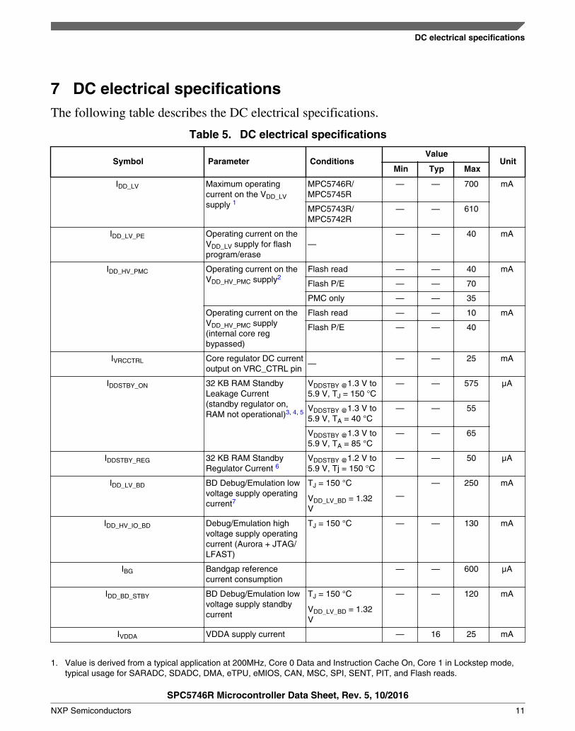
7 DC electrical specificationsThe following table describes the DC electrical specifications.
Table 5. DC electrical specifications
Symbol Parameter ConditionsValue
UnitMin Typ Max
IDD_LV Maximum operatingcurrent on the VDD_LVsupply 1
MPC5746R/MPC5745R
— — 700 mA
MPC5743R/MPC5742R
— — 610
IDD_LV_PE Operating current on theVDD_LV supply for flashprogram/erase
—— — 40 mA
IDD_HV_PMC Operating current on theVDD_HV_PMC supply2
Flash read — — 40 mA
Flash P/E — — 70
PMC only — — 35
Operating current on theVDD_HV_PMC supply(internal core regbypassed)
Flash read — — 10 mA
Flash P/E — — 40
IVRCCTRL Core regulator DC currentoutput on VRC_CTRL pin
—— — 25 mA
IDDSTBY_ON 32 KB RAM StandbyLeakage Current(standby regulator on,RAM not operational)3, 4, 5
VDDSTBY @1.3 V to5.9 V, TJ = 150 °C
— — 575 µA
VDDSTBY @1.3 V to5.9 V, TA = 40 °C
— — 55
VDDSTBY @1.3 V to5.9 V, TA = 85 °C
— — 65
IDDSTBY_REG 32 KB RAM StandbyRegulator Current 6
VDDSTBY @1.2 V to5.9 V, Tj = 150 °C
— — 50 µA
IDD_LV_BD BD Debug/Emulation lowvoltage supply operatingcurrent7
TJ = 150 °C
VDD_LV_BD = 1.32V
—
— 250 mA
IDD_HV_IO_BD Debug/Emulation highvoltage supply operatingcurrent (Aurora + JTAG/LFAST)
TJ = 150 °C — — 130 mA
IBG Bandgap referencecurrent consumption
— — 600 µA
IDD_BD_STBY BD Debug/Emulation lowvoltage supply standbycurrent
TJ = 150 °C
VDD_LV_BD = 1.32V
— — 120 mA
IVDDA VDDA supply current — 16 25 mA
1. Value is derived from a typical application at 200MHz, Core 0 Data and Instruction Cache On, Core 1 in Lockstep mode,typical usage for SARADC, SDADC, DMA, eTPU, eMIOS, CAN, MSC, SPI, SENT, PIT, and Flash reads.
DC electrical specifications
SPC5746R Microcontroller Data Sheet, Rev. 5, 10/2016
NXP Semiconductors 11
2. This value is considering the use of the internal core regulator with an external ballast with the minimum value of hFE of 60.3. Data is retained for full TB range of -40 °C to 125 °C. RAM supply switch to the standby regulator occurs when the VDD_LV
supply falls below 0.95V.4. VDDSTBY may be supplied with a non-regulated power supply, but the absolute maximum voltage on VDDSTBY given in the
absolute maximum ratings table must be observed.5. The maximum value for IDDSTBY_ON is also valid when switching from the core supply to the standby supply, and when
powering up the device and switching the RAM supply back to VDD_LV6. When the VDDSTBY pin is powered, the standby RAM regulator current is present on the pin, regardless if the device is in
standby mode or not. No current is present on the pin when VDDSTBY pin is set to 0V, disabling the standby regulator.7. Worst case usage (data trace, data overlay, full Aurora utilization).
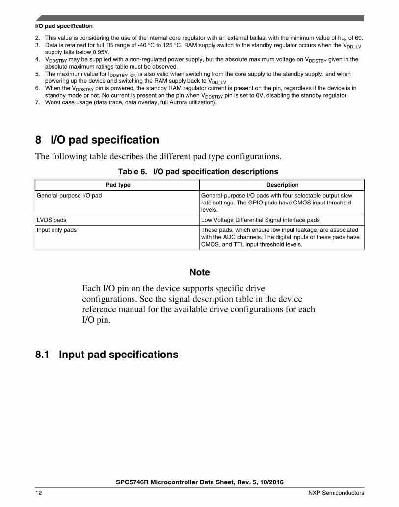
8 I/O pad specificationThe following table describes the different pad type configurations.
Table 6. I/O pad specification descriptions
Pad type Description
General-purpose I/O pad General-purpose I/O pads with four selectable output slewrate settings. The GPIO pads have CMOS input thresholdlevels.
LVDS pads Low Voltage Differential Signal interface pads
Input only pads These pads, which ensure low input leakage, are associatedwith the ADC channels. The digital inputs of these pads haveCMOS, and TTL input threshold levels.
Note
Each I/O pin on the device supports specific driveconfigurations. See the signal description table in the devicereference manual for the available drive configurations for eachI/O pin.
8.1 Input pad specifications
I/O pad specification
SPC5746R Microcontroller Data Sheet, Rev. 5, 10/2016
12 NXP Semiconductors

VIL
VIN
VDD
VIH
VINTERNAL
VHYS
(SIUL register)
Figure 3. I/O input DC electrical characteristics definition
Table 7. I/O input DC electrical characteristics
Symbol Parameter1 Conditions Value2 Unit
Min Typ Max
VIHTTL TTL input high level 3.0 V < VDD_HV_IO < 5.5 V 2.0 — VDD_HV_IO +0.3
V
VILTTL TTL input low level 3.0 V < VDD_HV_IO < 5.5 V VSS -0.3 — 0.6 V
VHYSTTL TTL level input hysteresis 3.0 V < VDD_HV_IO < 5.5 V 0.3 — — V
VDRFTTTL TTL Input VIL/VIHtemperature drift
— — — 1003 mV
VIHCMOS_H CMOS input high level(with hysteresis)
3.0 V < VDD_HV_IO < 5.5 V 0.65 *VDD_HV_IO
— VDD_HV_IO
+ 0.3
V
VIHCMOS CMOS input high level(without hysteresis)
3.0 V < VDD_HV_IO < 5.5 V 0.55 *VDD_HV_IO
— VDD_HV_IO +0.3
V
VILCMOS_H CMOS input low level (withhysteresis)
3.0 V < VDD_HV_IO < 5.5 V VSS -0.3 — 0.35 *
VDD_HV_IO
V
VILCMOS CMOS input low level(without hysteresis)
3.0 V < VDD_HV_IO < 5.5 V VSS -0.3 — 0.4 *
VDD_HV_IO
V
VHYSCMOS CMOS input hysteresis 3.0 V < VDD_HV_IO < 5.5 V 0.1 *
VDD_HV_IO
— — V
VDRFTCMOS
CMOS Input VIL/VIHtemperature drift
— — — 1003 mV
INPUT CHARACTERISTICS4
ILKG Digital input leakage GPIO pins
VSS < VIN < VDD_HV_IO
-1.0 — 1.0 µA
CIN Input capacitance GPIO and Input pins — — 8 pF
1. Supported input levels vary according to pad types. Pad type "pad_sr_hv" supports only the CMOS input level, while padtype "pad_isatww_st_hv" supports TTL and CMOS levels. Refer to the IO spreadsheet attached to the Reference Manualfor the pad type of each pin.
I/O pad specification
SPC5746R Microcontroller Data Sheet, Rev. 5, 10/2016
NXP Semiconductors 13

2. TTL level input specifications apply to the digital inputs on the analog input pins, and not the GPIO pins on the device.3. In a 1 ms period, assuming stable voltage and a temperature variation of ±30 °C, VIL/VIH shift is within ±50 mV. For
SENT requirement, refer to Note in the "I/O pad current specifications" section.4. For LFAST, microsecond bus, and LVDS input characteristics, refer to dedicated communication module chapters.
The following table provides the current specifications for the GPIO pad weak pull-upand pull-down.
Table 8. GPIO Pull-Up/Down DC electrical characteristics
Symbol Parameter Conditions Value Unit
Min Typ Max
|IWPU| Weak pull-up currentabsolute value1
Vin = VIH = 0.65 * VDD_HV_IO µA
4.5V < VDD_HV_IO < 5.5V 30 — —
3.0V < VDD_HV_IO < 3.6V 18 — —
Vin = VIL = 0.35 * VDD_HV_IO
4.5V < VDD_HV_IO < 5.5V — — 120
3.0V < VDD_HV_IO < 3.6V — — 80
Vin = VIL = 1.1V (TTL)
4.5V < VDD_HV_IO < 5.5V — — 130
|IWPD| Weak pull-down currentabsolute value
Vin = VIH = 0.65 * VDD_HV_IO µA
4.5V < VDD_HV_IO < 5.5V — — 120
3.0V < VDD_HV_IO < 3.6V — — 80
Vin = VIL = 0.35 * VDD_HV_IO
4.5V < VDD_HV_IO < 5.5V 30 — —
3.0V < VDD_HV_IO < 3.6V 18 — —
Vin = VIL = 0.9V (TTL)
4.5V < VDD_HV_IO < 5.5V 16 — —
1. Weak pull-up/down is enabled within tWK_PU = 1 µs after internal/external reset has been asserted. Output voltage willdepend on the amount of capacitance connected to the pin.
I/O pad specification
SPC5746R Microcontroller Data Sheet, Rev. 5, 10/2016
14 NXP Semiconductors

DD_HV_IOV
VDD_POR
RESET(INTERNAL)
pull-upenabled
RESET
YES
NO
PAD
POWER-UP Application defined Application defined POWER-DOWN
tWK_PU tWK_PU
(1)(1)
(1)
1 Actual PAD slopes will depend on external capacitances and VDD_HV_IO supply.
Figure 4. Weak pull-up electrical characteristics definition
Analog input leakage and pull up/down information is located in the ADC inputdescription section.
8.2 Output pad specifications
The following figure provides the description of output DC electrical characteristics.
I/O pad specification
SPC5746R Microcontroller Data Sheet, Rev. 5, 10/2016
NXP Semiconductors 15

10%
Vout
VINTERNAL
VHYS
(SIUL2 register)
20%
80% 90%
tR10-90
tR20-80
tF10-90
tF20-80
tTR(max) = MAX(tR10-90;tF10-90) tTR(min) = MIN(tR10-90;tF10-90) tTR20-80(max) = MAX(tR20-80;tF20-80)
tTR20-80(min) = MIN(tR20-80;tF20-80) tSKEW20-80 = tR20-80-tF20-80
tSKEW20-80
50%
tPD tPD
Figure 5. I/O output DC electrical characteristics definition
Table 9. GPIO pad output buffer electrical characteristics
Symbol Parameter Conditions Value 1, 2 Unit
Min Typ Max
VOH GPIO pad output high voltage 4.5V < VDD_HV_IO < 5.0V
MSCR[OERC] = 11, IOH = 38mA
MSCR[OERC] = 10, IOH = 19mA
MSCR[OERC] = 01, IOH = 10mA
MSCR[OERC] = 00, IOH = 5mA
0.8 *VDD_HV_IO
— — V
3.0V < VDD_HV_IO < 3.6V
MSCR[OERC] = 11, IOH = 19mA
MSCR[OERC] = 10, IOH = 10mA
MSCR[OERC] = 01, IOH = 7mA
MSCR[OERC] = 00, IOH = 5mA
0.8 *VDD_HV_IO
— —
VOL GPIO pad output low voltage 4.5V < VDD_HV_IO < 5.0V
MSCR[OERC] = 11, IOL = 48mA
MSCR[OERC] = 10, IOL = 24mA
MSCR[OERC] = 01, IOL = 12mA
— — 0.2 *VDD_HV_IO
V
Table continues on the next page...
I/O pad specification
SPC5746R Microcontroller Data Sheet, Rev. 5, 10/2016
16 NXP Semiconductors
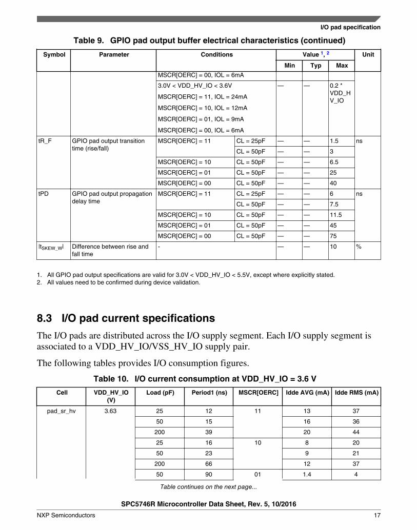
Table 9. GPIO pad output buffer electrical characteristics (continued)
Symbol Parameter Conditions Value 1, 2 Unit
Min Typ Max
MSCR[OERC] = 00, IOL = 6mA
3.0V < VDD_HV_IO < 3.6V
MSCR[OERC] = 11, IOL = 24mA
MSCR[OERC] = 10, IOL = 12mA
MSCR[OERC] = 01, IOL = 9mA
MSCR[OERC] = 00, IOL = 6mA
— — 0.2 *VDD_HV_IO
tR_F GPIO pad output transitiontime (rise/fall)
MSCR[OERC] = 11 CL = 25pF — — 1.5 ns
CL = 50pF — — 3
MSCR[OERC] = 10 CL = 50pF — — 6.5
MSCR[OERC] = 01 CL = 50pF — — 25
MSCR[OERC] = 00 CL = 50pF — — 40
tPD GPIO pad output propagationdelay time
MSCR[OERC] = 11 CL = 25pF — — 6 ns
CL = 50pF — — 7.5
MSCR[OERC] = 10 CL = 50pF — — 11.5
MSCR[OERC] = 01 CL = 50pF — — 45
MSCR[OERC] = 00 CL = 50pF — — 75
|tSKEW_W| Difference between rise andfall time
- — — 10 %
1. All GPIO pad output specifications are valid for 3.0V < VDD_HV_IO < 5.5V, except where explicitly stated.2. All values need to be confirmed during device validation.
8.3 I/O pad current specifications
The I/O pads are distributed across the I/O supply segment. Each I/O supply segment isassociated to a VDD_HV_IO/VSS_HV_IO supply pair.
The following tables provides I/O consumption figures.
Table 10. I/O current consumption at VDD_HV_IO = 3.6 V
Cell VDD_HV_IO(V)
Load (pF) Period1 (ns) MSCR[OERC] Idde AVG (mA) Idde RMS (mA)
pad_sr_hv 3.63 25 12 11 13 37
50 15 16 36
200 39 20 44
25 16 10 8 20
50 23 9 21
200 66 12 37
50 90 01 1.4 4
Table continues on the next page...
I/O pad specification
SPC5746R Microcontroller Data Sheet, Rev. 5, 10/2016
NXP Semiconductors 17

Table 10. I/O current consumption at VDD_HV_IO = 3.6 V (continued)
Cell VDD_HV_IO(V)
Load (pF) Period1 (ns) MSCR[OERC] Idde AVG (mA) Idde RMS (mA)
200 130 3 9
50 150 00 1.6 4
200 200 4 11
Table 11. I/O current consumption at VDD_HV_IO = 5.5 V
Cell VDD_HV_IO(V)
Load (pF) Period1 (ns) MSCR[OERC] Idde AVG (mA) Idde RMS (mA)
pad_sr_hv 5.5 25 9 11 37 83
50 10.2 42 89
200 26 46 92
25 10.5 10 25 53
50 16 21 44
200 44 26 49
50 54 01 6 14
200 80 15 35
50 80 00 4 9
200 130 9 22
In order to ensure device reliability, the average current of the I/O on a single segmentshould remain below the IMAXSEG value given in the table "Absolute maximum ratings".
In order to ensure device functionality, the sum of the dynamic and static current of theI/O on a single segment should remain below the IMAXSEG value given in the table"Device operating conditions".
Note
The MPC5746R I/O Signal Description and Input MultiplexingTables are contained in a Microsoft Excel workbook fileattached to the Reference Manual.
9 Reset pad (PORST, RESET) electrical characteristicsThe device implements a dedicated bidirectional reset pin (PORST).
Reset pad (PORST, RESET) electrical characteristics
SPC5746R Microcontroller Data Sheet, Rev. 5, 10/2016
18 NXP Semiconductors

NOTE
PORST pin does not require active control. It is possible toimplement an external pull-up to ensure correct reset exitsequence. Recommended value is 4.7 kohm.
PORST can optionally be connected to an external power-onsupply circuitry.
No restrictions exist on reset signal slew rate apart fromabsolute maximum rating compliance.
VIL
VDD
VDDMIN
PORST
VIH
device start-up phase
VDDPOR
PORST driven low device reset forced by external circuitry
PORST undriven device reset by by internal power-on reset internal power-on reset
Figure 6. Start-up reset requirements
The following figure describes device behavior depending on supply signal on PORST:
1. PORST low pulse amplitude is too low—it is filtered by input buffer hysteresis.Device remains in current state.
2. PORST low pulse duration is too short—it is filtered by a low pass filter. Deviceremains in current state.
3. PORST low pulse is generating a reset:• a) PORST low but initially filtered during at least WFRST. Device remains
initially in current state.• b) PORST potentially filtered until WNFRST. Device state is unknown. It may
either be reset or remains in current state depending on extra condition(temperature, voltage, device).
• c) PORST asserted for longer than WNFRST. Device is under reset.
Reset pad (PORST, RESET) electrical characteristics
SPC5746R Microcontroller Data Sheet, Rev. 5, 10/2016
NXP Semiconductors 19

VPORST
VIL
VIH
VDD
filtered by hyst er esi s
filtered by lowp ass filter
WFRSTWNFRST
filtered by lowp ass filter
WFRST
unknown reset state device under hardware reset
internal reset
1 2 3a 3b 3c
VHYS
Figure 7. Noise filtering on reset signal
Table 12. Reset electrical characteristics
Symbol Parameter Conditions Value1 Unit
Min Typ Max
VIH Reset Input high level TTL 3.5 V < VDD_HV_IO < 5.5 V 2.0 — VDD_HV_IO +0.3
V
VIL Reset Input low level TTL 3.5 V < VDD_HV_IO < 3.6 V VSS - 0.3 — 0.6 V
4.5 V < VDD_HV_IO < 5.5 V VSS - 0.3 — 0.8
VHYSReset
Input hysteresis TTL 3.5 V < VDD_HV_IO < 5.5 V 300 — — mV
VIHPORST
Input high level CMOS 3.5 V < VDD_HV_IO < 5.5 V 0.65 *VDD_HV_IO
— VDD_HV_IO +0.3
V
VILPORST
Input low level CMOS 3.5 V < VDD_HV_IO < 5.5 V VSS - 0.3 — 0.35 *VDD_HV_IO
V
VHYSPORST
Input hysteresis CMOS 3.5 V < VDD_HV_IO < 5.5 V 0.1 *VDD_HV_IO
— — mV
VDD_POR Minimum supply for strong pulldownactivation
— — — 1.2 V
Table continues on the next page...
Reset pad (PORST, RESET) electrical characteristics
SPC5746R Microcontroller Data Sheet, Rev. 5, 10/2016
20 NXP Semiconductors
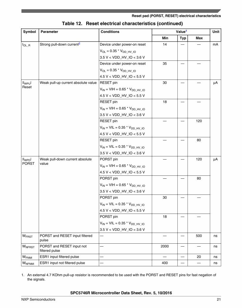
Table 12. Reset electrical characteristics (continued)
Symbol Parameter Conditions Value1 Unit
Min Typ Max
IOL_R Strong pull-down current2 Device under power-on reset
VOL = 0.35 * VDD_HV_IO
3.5 V < VDD_HV_IO < 3.6 V
14 — — mA
Device under power-on reset
VOL = 0.35 * VDD_HV_IO
4.5 V < VDD_HV_IO < 5.5 V
35 — —
|IWPU|Reset
Weak pull-up current absolute value RESET pin
VIN = VIH = 0.65 * VDD_HV_IO
4.5 V < VDD_HV_IO < 5.5 V
30 — — μA
RESET pin
VIN = VIH = 0.65 * VDD_HV_IO
3.5 V < VDD_HV_IO < 3.6 V
18 — —
RESET pin
VIN = VIL = 0.35 * VDD_HV_IO
4.5 V < VDD_HV_IO < 5.5 V
— — 120
RESET pin
VIN = VIL = 0.35 * VDD_HV_IO
3.5 V < VDD_HV_IO < 3.6 V
— — 80
|IWPD|PORST
Weak pull-down current absolutevalue
PORST pin
VIN = VIH = 0.65 * VDD_HV_IO
4.5 V < VDD_HV_IO < 5.5 V
— — 120 μA
PORST pin
VIN = VIH = 0.65 * VDD_HV_IO
3.5 V < VDD_HV_IO < 3.6 V
— — 80
PORST pin
VIN = VIL = 0.35 * VDD_HV_IO
4.5 V < VDD_HV_IO < 5.5 V
30 — —
PORST pin
VIN = VIL = 0.35 * VDD_HV_IO
3.5 V < VDD_HV_IO < 3.6 V
18 — —
WFRST PORST and RESET input filteredpulse
— — — 500 ns
WNFRST PORST and RESET input notfiltered pulse
— 2000 — — ns
WFNMI ESR1 input filtered pulse — — — 20 ns
WNFNMI ESR1 input not filtered pulse — 400 — — ns
1. An external 4.7 KOhm pull-up resistor is recommended to be used with the PORST and RESET pins for fast negation ofthe signals.
Reset pad (PORST, RESET) electrical characteristics
SPC5746R Microcontroller Data Sheet, Rev. 5, 10/2016
NXP Semiconductors 21

2. Strong pull-down is enabled during power up / phase0 on both pads but after that a weak pull-down is enabled on PORSTand a weak pull-up is enabled on RESET.
10 Oscillator and FMPLLTwo on-chip PLLs, the peripheral clock and reference PLL (PLL0), and the frequencymodulated system PLL (PLL1) generate the system and auxiliary clocks from theexternal oscillator.
PLL0
PLL1
RCOSC
XOSC
PLL0_PHI0
PLL0_PHI1
PLL1_PHI0
Figure 8. PLL integration
Table 13. PLL0 electrical characteristics
Symbol Parameter ConditionsValue
UnitMin Typ Max
fPLL0IN PLL0 input clock1 — 8 — 40 MHz
ΔPLL0IN PLL0 input clock duty cycle1
— 40 — 60 %
fPLL0VCO PLL0 VCO frequency — 600 — 1250 MHz
fPLL0PHI0 PLL0 output clock PHI0 — 4.762 — 400 MHz
tPLL0LOCK PLL0 lock time — — — 110 µs
|Δ
PLL0PHI1SPJ|
PLL0_PHI1 single period jitter
fPLL0IN = 20 MHz (resonator)
fPLL0PHI1 = 40 MHz, 6-sigma
— — 3002 ps
ΔPLL0LTJ PLL0 output long term jitter2
fPLL0IN = 20 MHz (resonator), VCOfrequency = 800 MHz
10 periods accumulatedjitter (80 MHz frequency),6-sigma pk-pk
–250 — 250 ps
16 periods accumulatedjitter (50 MHz frequency),6-sigma pk-pk
–300 — 300 ps
long term jitter
(< 1MHz frequency), 6-sigma pk-pk
–650 — 650 ps
IPLL0 PLL0 consumption FINE LOCK state — — 5 mA
1. PLL0IN clock retrieved directly from either internal RCOSC or external FXOSC clock. Input characteristics are grantedwhen using internal RCOSC or external oscillator is used in functional mode.
Oscillator and FMPLL
SPC5746R Microcontroller Data Sheet, Rev. 5, 10/2016
22 NXP Semiconductors

2. VDD_LV noise due to application in the range VDD_LV = 1.25V (+/-5%) with frequency below PLL bandwidth (40 KHz) will befiltered.
Table 14. FMPLL1 electrical characteristics
Symbol Parameter ConditionsValue
UnitMin Typ Max
fPLL1IN PLL1 input clock1 — 38 — 78 MHz
ΔPLL1IN PLL1 input clock duty cycle1
— 35 — 65 %
fPLL1VCO PLL1 VCO frequency — 600 — 1250 MHz
fPLL1PHI0 PLL1 output clock PHI0 — 4.762 — 200 MHz
tPLL1LOCK PLL1 lock time — — — 100 µs
fPLL1MOD PLL1 modulation frequency — — — 250 kHz
|δ PLL1MOD| PLL1 modulation depth (when enabled) Center spread 0.25 — 2 %
Down spread 0.5 — 4 %
|Δ
PLL1PHI0SPJ|
PLL1_PHI0 single period peak to peakjitter
fPLL1PHI0 = 200 MHz, 6-sigma pk-pk
— — 5002 ps
IPLL1 PLL1 consumption FINE LOCK state — — 6 mA
1. PLL1IN clock retrieved directly from either internal PLL0 or external XOSC clock. Input characteristics are granted whenusing internal PLL0 or external oscillator is used in functional mode.
2. 1.25V +/-5%, application noise below 40kHz at VDD_LV pin - no frequency modulation
All oscillator specifications are valid for VDD_HV_IO_JTAG = 3.0 V to 5.5 V.
Table 15. XOSC External Oscillator electrical specifications
Symbol Parameter ConditionsValue Unit
Min Max
fXTAL Crystal Frequency Range1 — 4 8 MHz
— >8 20
16MHz < freq < 40MHz (at present, freq =20M and 40M have been validated, but stillneeds to be carried out for freq = 16MHz)
>20 40
tcst Crystal start-up time2, 3 TJ = 150 °C, 20 MHz ≤ f ≤ 40 MHz — 5 ms
trec Crystal recovery time4 — — 0.5 ms
VIHEXT EXTAL input high voltage5
(External Reference)VREF = 0.28 * VDD_HV_IO_JTAG VREF
+ 0.6— V
VILEXT EXTAL input low voltage(External Reference)
VREF = 0.28 * VDD_HV_IO_JTAG — VREF -0.6
V
CS_EXTAL Total on-chip stray capacitanceon EXTAL pin6
BGA 4.75 5.25 pF
QFP 5.25 5.75
CS_XTAL Total on-chip stray capacitanceon XTAL pin
6BGA 4.75 5.25 pF
QFP 5.25 5.75
gm Oscillator Transconductance TJ = -40 °C to 150°C
fXTAL ≤ 8 MHz 3 13 mA/V
fXTAL ≤ 20 MHz 9 35
Table continues on the next page...
Oscillator and FMPLL
SPC5746R Microcontroller Data Sheet, Rev. 5, 10/2016
NXP Semiconductors 23

Table 15. XOSC External Oscillator electrical specifications(continued)
Symbol Parameter ConditionsValue Unit
Min Max
fXTAL ≤ 40 MHz 12 43
VEXTAL Oscillation Amplitude on theEXTAL pin after startup7
TJ = –40 °C to 150°C
0.5 1.6 V
IXTAL XTAL current7,8 TJ = –40 °C to 150°C
— 14 mA
1. The range is selectable by UTEST miscellaneous DCF clients XOSC_LF_EN and XOSC_EN_40MHZ.2. This value is determined by the crystal manufacturer and board design.3. Proper PC board layout procedures must be followed to achieve specifications.4. Crystal recovery time is the time for the oscillator to settle to the correct frequency after adjustment of the integrated load
capacitor value.5. This parameter is guaranteed by design rather than 100% tested.6. See crystal manufacturer's specification for recommended load capacitor (CL) values.The external oscillator requires
external load capacitors when operating from 8 MHz to 16 MHz. Account for on-chip stray capacitance (CS_EXTAL/CS_XTAL)and PCB capacitance when selecting a load capacitor value. When operating at 20 MHz/40 MHz, the integrated loadcapacitor value is selected via S/W to match the crystal manufacturer's specification, while accounting for on-chip and PCBcapacitance. The capacitance on “EXTAL” and “XTAL” by internal capacitance array is controlled by the XOSC LOAD CAPSEL field of the UTEST Miscellaneous DCF client. See the DCF Records chapter of the Reference Manual.
7. Amplitude on the EXTAL pin after startup is determined by the ALC block, i.e., the Automatic Level Control Circuit. Thefunction of the ALC is to provide high drive current during oscillator startup, but reduce current after oscillation in order toreduce power, distortion, and RFI, and to avoid overdriving the crystal. The operating point of the ALC is dependent on thecrystal value and loading conditions.
8. IXTAL is the oscillator bias current out on the XTAL pin with both EXTAL and XTAL pins grounded. This is the maximumcurrent during startup of the oscillator. The current after oscillation is typically in the 2-3 mA range and is dependant on theload and series resistance of the crystal. Test circuit is shown in the figure below.
Table 16. Selectable load capacitance
load_cap_sel[4:0] from DCF record Capacitance on EXTAL (CEXTAL)/XTAL (CXTAL) , 1, 2 (pF)
00000 1.0
00001 2.0
00010 2.9
00011 3.8
00100 4.8
00101 5.7
00110 6.6
00111 7.5
01000 8.5
01001 9.4
01010 10.3
01011 11.2
01100 12.2
01101 13.1
01110 14.0
Table continues on the next page...
Oscillator and FMPLL
SPC5746R Microcontroller Data Sheet, Rev. 5, 10/2016
24 NXP Semiconductors

Table 16. Selectable load capacitance (continued)
load_cap_sel[4:0] from DCF record Capacitance on EXTAL (CEXTAL)/XTAL (CXTAL) , 1, 2 (pF)
01111 15.0
10000-11111 N/A
1. Values are determined from simulation across process corners and voltage and temperature variation. Capacitance valuesvary ±12% across process, 0.25% across voltage, and no variation across temperature.
2. Values in this table do not include the internal stray capacitances Cxtal/Cextal.
V
A
IXTAL
Bias
XTAL
EXTAL
VSSOSC
VSS
TesterPCBGND
Current
Comparator
OFF
Z = R + j LConditions
VVALC INACTIVE
EXTAL
XTAL
=0 V=0 V
V
ALC
DDOSC
Figure 9. Test circuit
Table 17. Internal RC Oscillator electrical specifications
Symbol Parameter ConditionsValue
UnitMin Typ Max
fTarget IRCOSC target frequency — — 16 — MHz
δfvar_noT IRC frequency variation withouttemperature compensation
T < 150 °C –8 — 8 %
δfvar_T IRC frequency variation withtemperature compensation
T < 150 °C –3 — 3 %
δfvar_SW IRC software trimming accuracy Trimmingtemperature
–1 — 1 %
δfTRIM IRC software trimming step — — +40/-48 — kHz
Tstart_noT Startup time to reach within fvar_noT Factory trimmingalready applied
— — 5 µs
Tstart_T Startup time to reach within fvar_T Factory trimmingalready applied
— — 120 µs
Table continues on the next page...
Oscillator and FMPLL
SPC5746R Microcontroller Data Sheet, Rev. 5, 10/2016
NXP Semiconductors 25

Table 17. Internal RC Oscillator electrical specifications (continued)
Symbol Parameter ConditionsValue
UnitMin Typ Max
IAVDD5 Current consumption on 5 V powersupply
After Tstart_T — — 400 µA
IDVDD12 Current consumption on 1.2 V powersupply
After Tstart_T — — 175 µA
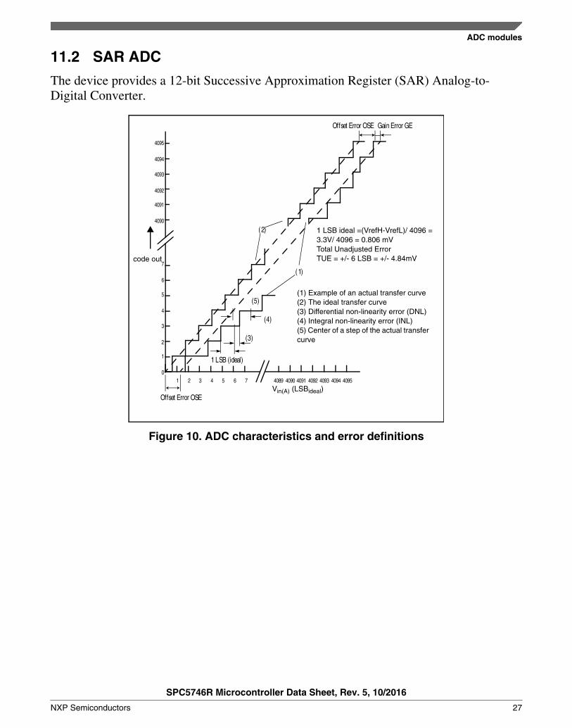
11 ADC modulesThis device's analog sub-system contains a total of four independent 12-bit SuccessiveApproximation (SAR) ADCs and three independent 16-bit Sigma-Delta (S/D) ADCs.
11.1 ADC input description
The following table provides the current specifications for the analog input pad weakpull-up and pull-down, and the resistance for the analog input bias/diagnostic pull up/down.
Table 18. Analog Input Leakage and Pull-Up/Down DC electrical characteristics
Symbol Parameter Conditions Value Unit
Min Typ Max
ILK_AD Analog input leakagecurrent
Input channel off
4.5V < VDD_HV_IO < 5.5V
VSS_HV_ADV_SAR < VIN <VDD_HV_ADV_SAR
VSS_HV_ADV_SD < VIN < VDD_HV_ADV_SD
-200 — 200 nA
RPUPD Analog input bias/diagnostic pull up/downresistance
200KΩ
3.0V < VDD_HV_IO < 5.5V
130 200 280 KΩ
100KΩ
3.0V < VDD_HV_IO < 5.5V
65 100 140
5KΩ
3.0V < VDD_HV_IO < 5.5V
1.4 5 8.8
ΔPUPD RPUPD pull up/downresistance mismatch
3.0V < VDD_HV_IO < 5.5V — — 5 %
ADC modules
SPC5746R Microcontroller Data Sheet, Rev. 5, 10/2016
26 NXP Semiconductors
11.2 SAR ADC
The device provides a 12-bit Successive Approximation Register (SAR) Analog-to-Digital Converter.
(2 )
(1)
(3 ) (4)
(5)
Offset Error OSE
Offset Error OSE
Gain Error GE
1 LSB (ideal)
Vin(A) (LSBideal)
(1) Example of an actual transfer curve (2) The ideal transfer curve (3) Differential non-linearity error (DNL) (4) Integral non-linearity error (INL) (5) Center of a step of the actual transfer curve
code out
4095 4094 4093 4092 4091 4090
5 4 3 2 1
0
7 6
1 2 3 4 5 6 7 4089 4090 4091 4092 4093 4094 4095
1 LSB ideal =(VrefH-VrefL)/ 4096 = 3.3V/ 4096 = 0.806 mV Total Unadjusted Error TUE = +/- 6 LSB = +/- 4.84mV
Figure 10. ADC characteristics and error definitions
ADC modules
SPC5746R Microcontroller Data Sheet, Rev. 5, 10/2016
NXP Semiconductors 27

11.2.1 Input equivalent circuit and ADC conversion characteristics
RF
CF
RS RL RSW1
CP2
VDD_HV_IO
Sampling Source Filter Current Limiter
EXTERNAL CIRCUIT INTERNAL CIRCUIT SCHEME
RS Source Impedance RF Filter Resistance CF Filter Capacitance RL Current Limiter Resistance RSW1 Channel Selection Switch Impedance RAD Sampling Switch Impedance CP Pin Capacitance (two contributions, CP1 and CP2) CS Sampling Capacitance
CP1
RAD
Channel Selection
VA CS
Figure 11. Input equivalent circuit
Table 19. ADC conversion characteristics
Symbol Parameter Conditions1 Min Typ Max Unit
fCK, 2 ADC Clock frequency (depends
on ADC configuration) (The dutycycle depends on AD_CK3
frequency.)
— 20 — 80 MHz
fs Sampling frequency — — — 1.00 MHz
tsample Sample time4 — 250 — — ns
tconv Conversion time5 80 MHz 700 — — ns
CS, 6 ADC input sampling capacitance — — 3 5 pF
CP16 ADC input pin capacitance 1 — — — 5 pF
CP26 ADC input pin capacitance 2 — — — 0.8 pF
RSW16 Internal resistance of analog
sourceVREF range = 4.5 to 5.5 V — — 0.3 kΩ
VREF range = 3.0 to 3.6 V — — 875 Ω
RAD6 Internal resistance of analog
source— — — 825 Ω
INL Integral non-linearity — –2 — 2 LSB
DNL Differential non-linearity — –1 — 1 LSB
OFS7 Offset error — –6 — 6 LSB
GNE7 Gain error — –6 — 6 LSB
Input (double ADCchannel)
Max leakage 150 °C — — 300 nA
Table continues on the next page...
ADC modules
SPC5746R Microcontroller Data Sheet, Rev. 5, 10/2016
28 NXP Semiconductors

Table 19. ADC conversion characteristics (continued)
Symbol Parameter Conditions1 Min Typ Max Unit
SNR Signal-to-noise ratio VREF = 3.3 V, Fin ≤ 125kHz
66 — — dB
SNR Signal-to-noise ratio VREF = 5.0 V, Fin ≤ 125kHz
68 — — dB
THD Total harmonic distortion @ 125 kHz 65 70 — dB
ENOB8 Effective number of bits Fin < 125 kHz 10.5 — — bits
SINAD Signal-to-noise and distortion Fin < 125 kHz (6.02*ENOB)+1.76 dB
TUEIS1WINJ Total unadjusted error forIS1WINJ
Without current injection –6 — 6 LSB
TUEIS1WWINJ Total unadjusted error forIS1WWINJ
Without current injection –6 — 6 LSB
IDD_VDDA Maximum operating current onVDDA
Tj = 150C VDD_LV_COR= 1.32 V
— 3.7 5 mA
IDD_VDDR Maximum operating current onVREF
Tj = 150C VDD_LV_COR= 1.32 V
— 150 600 μA
VBG_REF, 9 Band gap reference for self test Trimmed,
INPSAMP=0xFF1.164 —10 1.236 V
1. VDD_HV_IO = 3.3 V -5%,+10%, TJ = –40 to +150 °C, unless otherwise specified, and analog input voltage from VAGND toVAREF
2. SAR ADC performance is not guaranteed when IRC is used as clock source for PLL0 to generate SAR ADC clock.3. AD_CK clock is always half of the ADC module input clock defined via the auxiliary clock divider for the ADC.4. During the sample time the input capacitance CS can be charged/discharged by the external source. The internal
resistance of the analog source must allow the capacitance to reach its final voltage level within tsample. After the end of thesample time tsample, changes of the analog input voltage have no effect on the conversion result. Values for the sampleclock tsample depend on programming.
5. This parameter does not include the sample time tsample, but only the time for determining the digital result and the time toload the result register with the conversion result.
6. See the above figure.7. Subject to change with additional -40°C characterization on final silicon version.8. Below 4.5V, ENOB - 9.5b, THD- 60dB at Fin= 125KHz9. Band gap reference only applies to Cut 2 silicon.10. Minimum and maximum values are typical +/-3%
NOTE• For spec complaint operation, do not expose clock sources,
including crystal oscillator, IRC, PLL0, and PLL1 on theCLKOUT pads while the SAR ADC is converting.
• The ADC performance specifications are not guaranteed iftwo or more ADCs simultaneously sample the same sharedchannel.
11.3 S/D ADC
The SD ADCs are Sigma Delta 16-bit analog-to-digital converters with 333 Kspsmaximum output rate.
ADC modules
SPC5746R Microcontroller Data Sheet, Rev. 5, 10/2016
NXP Semiconductors 29

Functional operating conditions are given in the DC electrical specifications. Absolutemaximum ratings are stress ratings only, and functional operation at the maxima is notguaranteed. Stress beyond the listed maxima may affect device reliability or causepermanent damage to the device.
Table 20. SDn ADC electrical specification
Symbol Parameter ConditionsValue
UnitMin Typ Max
VIN ADC input signal — 0 — VDD_HV_
ADV_SD
V
VIN_PK2PK1 Input range peak to
peak
VIN_PK2PK = VINP2 –
VINM, 3
Single ended.
VINM = VSS_HV_ADR_SD
VDD_HV_ADR_SD/GAINV
Single ended.
VINM = 0.5*VDD_HV_ADR_SD
GAIN = 1
±0.5*VDD_HV_ADR_SD
Single ended.
VINM = 0.5*VDD_HV_ADR_SD
GAIN = 2,4,8,16
±VDD_HV_ADR_SD/GAIN
Differential
0 < VIN < VDD_HV_IO_MAIN
±VDD_HV_ADR_SD/GAIN
fADCD_M S/D clock frequency TJ < 150 °C 4 14.4 16 MHz
fADCD_S Conversion rate TJ < 150 °C — — 333 ksps
— Oversampling ratio Internal modulator 24 — 256 —
RESOLUTION S/D register resolution 2's complement notation 164 bit
GAIN ADC gain Defined through ADC_SD[PGA] register.Only integer power of 2 are valid gain.
1 — 16 —
|δGAIN| Absolute value of theADC gain error5
Before calibration (applies to gainsettings =1)
— — 1 %
After calibration6
Δ VDD_HV_ADR_SD < 5%
Δ VDD_HV_ADV_SD < 10%
TJ < 50 °C
— — 0.1 %
After calibration6
Δ VDD_HV_ADR_SD < 5%
Δ VDD_HV_ADV_SD < 10%
TJ < 150 °C
— — 0.2 %
VOFFSET Conversion offset Before calibration
(applies to all gain settings – 1, 2, 4, 8,16)
— 10*
(1+1/gain)
20 mV
After calibration6 — — 5 mV
SNRDIFF150, 7 Signal to noise ratio in
differential mode 150ksps output rate
4.5 < VDD_HV_ADV_SD < 5.57
VDD_HV_ADR_D = VDD_HV_ADV_D
78 — — dB
Table continues on the next page...
ADC modules
SPC5746R Microcontroller Data Sheet, Rev. 5, 10/2016
30 NXP Semiconductors

Table 20. SDn ADC electrical specification (continued)
Symbol Parameter ConditionsValue
UnitMin Typ Max
GAIN = 1
TJ < 150 °C
4.5 < VDD_HV_ADV_SD < 5.57
VDD_HV_ADR_SD =
VDD_HV_ADV_SD
GAIN = 2
TJ < 150 °C
75 — —
4.5 < VDD_HV_ADV_SD < 5.57
VDD_HV_ADR_SD =
VDD_HV_ADV_SD
GAIN = 4
TJ < 150 °C
72 — —
4.5 < VDD_HV_ADV_SD < 5.57
VDD_HV_ADR_SD =
VDD_HV_ADV_SD
GAIN = 8
TJ < 150 °C
69 — —
4.5 < VDD_HV_ADV_SD < 5.57
VDD_HV_ADR_SD =
VDD_HV_ADV_SD
GAIN = 16
TJ < 150 °C
65 — —
SNRDIFF3337 Signal to noise ratio in
differential mode 333ksps output rate
4.5 < VDD_HV_ADV_SD < 5.57
VDD_HV_ADR_SD =
VDD_HV_ADV_SD
GAIN = 1
TJ < 150 °C
72 — — dB
4.5 < VDD_HV_ADV_SD < 5.57
VDD_HV_ADR_SD =
VDD_HV_ADV_SD
GAIN = 2
TJ < 150 °C
69 — —
4.5 < VDD_HV_ADV_SD < 5.57
VDD_HV_ADR_SD =
VDD_HV_ADV_SD
GAIN = 4
TJ < 150 °C
66 — —
Table continues on the next page...
ADC modules
SPC5746R Microcontroller Data Sheet, Rev. 5, 10/2016
NXP Semiconductors 31

Table 20. SDn ADC electrical specification (continued)
Symbol Parameter ConditionsValue
UnitMin Typ Max
4.5 < VDD_HV_ADV_SD < 5.57
VDD_HV_ADR_SD =
VDD_HV_ADV_SD
GAIN = 8
TJ < 150 °C
63 — —
4.5 < VDD_HV_ADV_SD < 5.57
VDD_HV_ADR_SD =
VDD_HV_ADV_SD
GAIN = 16
TJ < 150 °C
60 — —
SNRSE1507 Signal to noise ratio in
single ended mode 150ksps output rate
4.5 < VDD_HV_ADV_SD < 5.57
VDD_HV_ADR_SD =
VDD_HV_ADV_SD
GAIN = 1
TJ < 150 °C
72 — — dB
4.5 < VDD_HV_ADV_SD < 5.57
VDD_HV_ADR_SD =
VDD_HV_ADV_SD
GAIN = 2
TJ < 150 °C
69 — —
4.5 < VDD_HV_ADV_SD < 5.57
VDD_HV_ADR_SD =
VDD_HV_ADV_SD
GAIN = 4
TJ < 150 °C
66 — —
4.5 < VDD_HV_ADV_SD < 5.57
VDD_HV_ADR_SD =
VDD_HV_ADV_SD
GAIN = 8
TJ < 150 °C
63 — —
4.5 < VDD_HV_ADV_SD < 5.57
VDD_HV_ADR_DS =
VDD_HV_ADV_SD
GAIN = 16
TJ < 150 °C
55 — —
Table continues on the next page...
ADC modules
SPC5746R Microcontroller Data Sheet, Rev. 5, 10/2016
32 NXP Semiconductors

Table 20. SDn ADC electrical specification (continued)
Symbol Parameter ConditionsValue
UnitMin Typ Max
THDDIFF150 Total HarmonicDistortion in differentialmode 150 ksps outputrate
4.5 < VDD_HV_ADV_SD < 5.57
VDD_HV_ADR_D = VDD_HV_ADV_D
GAIN = 1
TJ < 150 °C
65 — — dB
4.5 < VDD_HV_ADV_SD < 5.57
VDD_HV_ADR_SD =
VDD_HV_ADV_SD
GAIN = 2
TJ < 150 °C
68 — —
4.5 < VDD_HV_ADV_SD < 5.57
VDD_HV_ADR_SD =
VDD_HV_ADV_SD
GAIN = 4
TJ < 150 °C
74 — —
4.5 < VDD_HV_ADV_SD < 5.57
VDD_HV_ADR_SD =
VDD_HV_ADV_SD
GAIN = 8
TJ < 150 °C
80 — —
4.5 < VDD_HV_ADV_SD < 5.57
VDD_HV_ADR_SD =
VDD_HV_ADV_SD
GAIN = 16
TJ < 150 °C
80 — —
THDDIFF333 Total HarmonicDistortion in differentialmode 333 ksps outputrate
4.5 < VDD_HV_ADV_SD < 5.57
VDD_HV_ADR_SD =
VDD_HV_ADV_SD
GAIN = 1
TJ < 150 °C
65 — — dB
4.5 < VDD_HV_ADV_SD < 5.57
VDD_HV_ADR_SD =
VDD_HV_ADV_SD
GAIN = 2
TJ < 150 °C
68 — —
4.5 < VDD_HV_ADV_SD < 5.57
VDD_HV_ADR_SD =
VDD_HV_ADV_SD
74 — —
Table continues on the next page...
ADC modules
SPC5746R Microcontroller Data Sheet, Rev. 5, 10/2016
NXP Semiconductors 33

Table 20. SDn ADC electrical specification (continued)
Symbol Parameter ConditionsValue
UnitMin Typ Max
GAIN = 4
TJ < 150 °C
4.5 < VDD_HV_ADV_SD < 5.57
VDD_HV_ADR_SD =
VDD_HV_ADV_SD
GAIN = 8
TJ < 150 °C
80 — —
4.5 < VDD_HV_ADV_SD < 5.57
VDD_HV_ADR_SD =
VDD_HV_ADV_SD
GAIN = 16
TJ < 150 °C
77 — —
THDSE150 Total HarmonicDistortion in singleended mode 150 kspsoutput rate
4.5 < VDD_HV_ADV_SD < 5.57
VDD_HV_ADR_SD =
VDD_HV_ADV_SD
GAIN = 1
TJ < 150 °C
68 — — dB
4.5 < VDD_HV_ADV_SD < 5.57
VDD_HV_ADR_SD =
VDD_HV_ADV_SD
GAIN = 2
TJ < 150 °C
68 — —
4.5 < VDD_HV_ADV_SD < 5.57
VDD_HV_ADR_SD =
VDD_HV_ADV_SD
GAIN = 4
TJ < 150 °C
68 — —
4.5 < VDD_HV_ADV_SD < 5.57
VDD_HV_ADR_SD =
VDD_HV_ADV_SD
GAIN = 8
TJ < 150 °C
68 — —
4.5 < VDD_HV_ADV_SD < 5.57
VDD_HV_ADR_DS =
VDD_HV_ADV_SD
GAIN = 16
TJ < 150 °C
68 — —
Table continues on the next page...
ADC modules
SPC5746R Microcontroller Data Sheet, Rev. 5, 10/2016
34 NXP Semiconductors

Table 20. SDn ADC electrical specification (continued)
Symbol Parameter ConditionsValue
UnitMin Typ Max
SINADDIFF150 Signal to NoiseDistortion Ratio indifferential mode 150ksps output rate
4.5 < VDD_HV_ADV_SD < 5.57
VDD_HV_ADR_D = VDD_HV_ADV_D
GAIN = 1
TJ < 150 °C
72 — — dB
4.5 < VDD_HV_ADV_SD < 5.57
VDD_HV_ADR_SD =
VDD_HV_ADV_SD
GAIN = 2
TJ < 150 °C
72 — —
4.5 < VDD_HV_ADV_SD < 5.57
VDD_HV_ADR_SD =
VDD_HV_ADV_SD
GAIN = 4
TJ < 150 °C
69 — —
4.5 < VDD_HV_ADV_SD < 5.57
VDD_HV_ADR_SD =
VDD_HV_ADV_SD
GAIN = 8
TJ < 150 °C
68.8 — —
4.5 < VDD_HV_ADV_SD < 5.57
VDD_HV_ADR_SD =
VDD_HV_ADV_SD
GAIN = 16
TJ < 150 °C
64.8 — —
SINADDIFF333 Signal to NoiseDistortion Ratio indifferential mode 333ksps output rate
4.5 < VDD_HV_ADV_SD < 5.57
VDD_HV_ADR_SD =
VDD_HV_ADV_SD
GAIN = 1
TJ < 150 °C
66 — — dB
4.5 < VDD_HV_ADV_SD < 5.57
VDD_HV_ADR_SD =
VDD_HV_ADV_SD
GAIN = 2
TJ < 150 °C
66 — —
4.5 < VDD_HV_ADV_SD < 5.57
VDD_HV_ADR_SD =
VDD_HV_ADV_SD
63 — —
Table continues on the next page...
ADC modules
SPC5746R Microcontroller Data Sheet, Rev. 5, 10/2016
NXP Semiconductors 35

Table 20. SDn ADC electrical specification (continued)
Symbol Parameter ConditionsValue
UnitMin Typ Max
GAIN = 4
TJ < 150 °C
4.5 < VDD_HV_ADV_SD < 5.57
VDD_HV_ADR_SD =
VDD_HV_ADV_SD
GAIN = 8
TJ < 150 °C
62 — —
4.5 < VDD_HV_ADV_SD < 5.57
VDD_HV_ADR_SD =
VDD_HV_ADV_SD
GAIN = 16
TJ < 150 °C
59 — —
SINADSE150 Signal to NoiseDistortion Ratio in singleended mode 150 kspsoutput rate
4.5 < VDD_HV_ADV_SD < 5.57
VDD_HV_ADR_SD =
VDD_HV_ADV_SD
GAIN = 1
TJ < 150 °C
66 — — dB
4.5 < VDD_HV_ADV_SD < 5.57
VDD_HV_ADR_SD =
VDD_HV_ADV_SD
GAIN = 2
TJ < 150 °C
66 — —
4.5 < VDD_HV_ADV_SD < 5.57
VDD_HV_ADR_SD =
VDD_HV_ADV_SD
GAIN = 4
TJ < 150 °C
63 — —
4.5 < VDD_HV_ADV_SD < 5.57
VDD_HV_ADR_SD =
VDD_HV_ADV_SD
GAIN = 8
TJ < 150 °C
62 — —
4.5 < VDD_HV_ADV_SD < 5.57
VDD_HV_ADR_DS =
VDD_HV_ADV_SD
GAIN = 16
TJ < 150 °C
54 — —
Table continues on the next page...
ADC modules
SPC5746R Microcontroller Data Sheet, Rev. 5, 10/2016
36 NXP Semiconductors

Table 20. SDn ADC electrical specification (continued)
Symbol Parameter ConditionsValue
UnitMin Typ Max
SFDR Spurious free dynamicrange
Any GAIN 60 — — dB
ZDIFF Differential inputimpedance8, 9
GAIN = 1 1000 1250 1500 kΩ
GAIN = 2 600 800 1000
GAIN = 4 300 400 500
GAIN = 8 200 250 300
GAIN = 16 200 250 300
ZCM Common Mode inputimpedance9, 10
GAIN = 1 1400 1800 2200 kΩ
GAIN = 2 1000 1300 1600
GAIN = 4 700 950 1150
GAIN = 8 500 650 800
GAIN = 16 500 650 800
RBIAS Bare bias resistance — 110 144 180 kΩ
ΔVINTCM Common Mode inputreference voltage11
— –12 — +12 %
VBIAS Bias voltage — — VDD_HV_
ADR_SD/2
— V
δVBIAS Bias voltage accuracy — –2.5 — +2.5 %
CMRR Common moderejection ratio
— 55 — — dB
— Anti-aliasing filter External series resistance — — 20 kΩ
Filter capacitances 220 — — pF
δRIPPLE Pass band ripple 12 0.333 * fADCD_S –1 — 1 %
— Stop band attenuation [0.5 * fADCD_S,
1.0 * fADCD_S]
40 — — dB
[1.0 * fADCD_S,
1.5 * fADCD_S]
45 — —
[1.5 * fADCD_S,
2.0 * fADCD_S]
50 — —
[2.0 * fADCD_S,
2.5 * fADCD_S]
55 — —
[2.5 * fADCD_S, fADCD_M/2] 60 — —
δGROUP Group delay Within pass band – Tclk is fADCD_M / 2 — — — —
OSR = 24 — — 235.5 Tclk
OSR = 28 — — 275
OSR = 32 — — 314.5
OSR = 36 — — 354
Table continues on the next page...
ADC modules
SPC5746R Microcontroller Data Sheet, Rev. 5, 10/2016
NXP Semiconductors 37

Table 20. SDn ADC electrical specification (continued)
Symbol Parameter ConditionsValue
UnitMin Typ Max
OSR = 40 — — 393.5
OSR = 44 — — 433
OSR = 48 — — 472.5
OSR = 56 — — 551.5
OSR = 64 — — 630.5
OSR = 72 — — 709.5
OSR = 75 — — 696
OSR = 80 — — 788.5
OSR = 88 — — 867.5
OSR = 96 — — 946.5
OSR = 112 — — 1104.5
OSR = 128 — — 1262.5
OSR = 144 — — 1420.5
OSR = 160 — — 1578.5
OSR = 176 — — 1736.5
OSR = 192 — — 1894.5
OSR = 224 — — 2210.5
OSR = 256 — — 2526.5
Distortion within pass band –0.5/
fADCD_S
— +0.5/
fADCD_S
—
fHIGH High pass filter 3dBfrequency
Enabled — 10e-5*
fADCD_S
— —
tSTARTUP Start-up time frompower down state
— — — 100 µs
tLATENCY Latency between inputdata and converted datawhen input mux doesnote change13
HPF = ON — — δGROUP+
fADCD_S
—
HPF = OFF — — δGROUP —
tSETTLING Settling time after muxchange
Analog inputs are muxed
HPF = ON
— — 2*δGROUP +3*fADCD_
S
—
HPF = OFF — — 2*δGROUP +2*fADCD_
S
—
tODRECOVERY Overdrive recovery time After input comes within range fromsaturation
HPF = ON
— — 2*δGROUP +fADCD_S
—
HPF = OFF — — 2*δGROUP
—
Table continues on the next page...
ADC modules
SPC5746R Microcontroller Data Sheet, Rev. 5, 10/2016
38 NXP Semiconductors

Table 20. SDn ADC electrical specification (continued)
Symbol Parameter ConditionsValue
UnitMin Typ Max
CS_D S/D ADC samplingcapacitance aftersampling switch14
GAIN = 1, 2, 4, 8 — — 75*GAIN
fF
GAIN = 16 — — 600 fF
IBIAS Bias consumption At least 1 ADCD enabled — — 3.5 mA
IADV_D ADCD supplyconsumption
ADCD enabled — 2.5 8 mA
ΣIADR_D Reference current forone SDADC
ADCD enabled — 10 50 µA
1. For input voltage above the maximum and below the clamp voltage of the input pad, there is no latch-up concern, and thesignal will only be 'clipped'.
2. VINP is the input voltage applied to the positive terminal of the SD ADC.3. VINM is the input voltage applied to the negative terminal of the SD ADC.4. For Gain=16, SDADC Resolution is 15 bit.5. Offset and gain error due to temperature drift can occur in either direction (+/-) for each of the SDADCs on the device.6. Calibration of gain is possible when gain = 1. Offset Calibration should be done with respect to 0.5*VDD_HV_ADR_SD for
differential "differential mode" and single ended mode with negative input=0.5*VDD_HV_ADR_SD ". Offset Calibration shouldbe done with respect to 0 for "single ended mode with negative input=0". Both Offset and Gain Calibration is guaranteedfor +/-5% variation of VDD_HV_ADR_SD, +/-10% variation of VDD_HV_ADV_SD, +/-50 C temperature variation.
7. S/D ADC is functional in the range 3.6V < VDD_HV_ADV_SD < 4.5V and 3.0V < VDD_HV_ADR_SD < 4.5 V, SNR paramterdegrades by 9 dB.
8. Input impedance in differential mode ZIN = ZDIFF9. Input impedance given at fADCD_M = 16 MHz. Impedance is inversely proportional to SDADC clock frequency. ZDIFF
(fADCD_M) = (16 MHz / fADCD_M) * ZDIFF, ZCM (fADCD_M) = (16 MHz / fADCD_M) * ZCM.10. Input impedance in single-ended mode ZIN = (2 * ZDIFF * ZCM) / (ZDIFF + ZCM)11. VINTCM is the Common Mode input reference voltage for the SDADC. It has a nominal value of (VRH_SD - VRL_SD) / 2.12. The ±1% passband ripple specification is equivalent to 20 * log10 (0.99) = 0.873 dB.13. Propagation of the information from the pin to the register CDR[CDATA] and flags SFR[DFEF], SFR[DFFF] is given by the
different modules that need to be crossed: delta/sigma filters, high pass filter, fifo module, clock domain synchronizers.The time elapsed between data availability at pin and internal S/D module registers is given by the following formula:REGISTER LATENCY = tLATENCY + 0.5/fADCD_S + 2 (~+1)/fADCD_M + 2(~+1)fPBRIDGEx_CLK where fADCD_S isthe frequency of the sampling clock, fADCD_M is the frequency of the modulator, and fPBRIDGEx_CLK is the frequencyof the peripheral bridge clock feeds to the ADC S/D module. The (~+1) symbol refers to the number of clock cyclesuncertainty (from 0 to 1 clock cycle) to be added due to resynchronization of the signal during clock domain crossing.Some further latency may be added by the target module (core, DMA, interrupt) controller to process the data receivedfrom the ADC S/D module.
14. This capacitance does not include pin capacitance, that can be considered together with external capacitance, beforesampling switch.
12 Temperature sensorThe following table describes the temperature sensor electrical characteristics.
Temperature sensor
SPC5746R Microcontroller Data Sheet, Rev. 5, 10/2016
NXP Semiconductors 39

Table 21. Temperature sensor electrical characteristics
Symbol Parameter ConditionsValue
UnitMin Typ Max
— Junction temperature monitoringrange
—–40 — 150 °C
TSENS Sensitivity — — 5.18 — mV/°C
TACC Accuracy — –7 — 7 °C
13 LVDS fast asynchronous serial transmission (LFAST) padelectrical characteristics
The LFAST pad electrical characteristics apply to both the LFAST and high-speed debugserial interfaces on the device. The same LVDS pad is used for the Microsecond Channel(MSC) and DSPI LVDS interfaces, with different characteristics given in the followingtables.
13.1 LFAST interface timing diagrams
LVDS fast asynchronous serial transmission (LFAST) pad electrical characteristics
SPC5746R Microcontroller Data Sheet, Rev. 5, 10/2016
40 NXP Semiconductors

Signal excursions above this level NOT allowed
Max. common mode input at RX
Maximum Differential Voltage
TX common mode
T = 1 / F
= 1.2 V +/- 10%
285 mV p-p (LFAST)400 mV p-p (MSC/DSPI)
150 mV p-p (MSC/SIPI)100 mV p-p (LFAST)Voltage =
V
Minimum Differential
Minimum Data Bit Time
Data Bit Period
Min. common mode input at RX
Signal excursions below this level NOT allowed
Opening =
"No-Go" Area
0.55 * T (LFAST)0.50 * T (MSC/SIPI)
DATA
VOD
VOD
1743 mV
1600 mV
150 mV
0 V
I
I I
I
OS
Figure 12. LFAST timing definition
LVDS fast asynchronous serial transmission (LFAST) pad electrical characteristics
SPC5746R Microcontroller Data Sheet, Rev. 5, 10/2016
NXP Semiconductors 41

Data Valid
Ifast_pwr_down
DifferentialData Lines pad_p/pad_n
TX
H
L
tPD2NM_TX
Figure 13. Power-down exit time
Differential
pad_p/pad_n
Data LinesTX
risefall
90%
10%
V
V
tt
IH
IL
Figure 14. Rise/fall time
13.2 LFAST and MSC /DSPI LVDS interface electricalcharacteristics
The following table contains the electrical characteristics for the LFAST interface.
The LVDS pad electrical characteristics in this table apply to both the LFAST and High-speed Debug (HSD) LVDS pad, and the MSC/DSPI LVDS pad except where noted in theconditions.
All LVDS pad electrical characteristics are valid from -40 °C to 150 °C.
LVDS fast asynchronous serial transmission (LFAST) pad electrical characteristics
SPC5746R Microcontroller Data Sheet, Rev. 5, 10/2016
42 NXP Semiconductors

Table 22. LVDS pad startup and receiver electrical characteristics
Symbol Parameter ConditionsValue
UnitMin Typ Max
tPD2NM_TX Transmitter startup time (powerdown to normal mode)1 —
— 0.4 0.55 µs
tSM2NM_TX Transmitter startup time (sleepmode to normal mode)2
Not applicable to the MSC/DSPI LVDS pad
— 0.2 0.5 µs
tPD2NM_RX Receiver startup time (power downto normal mode)3 —
— 20 40 ns
tPD2SM_RX Receiver startup time (power downto sleep mode)4
Not applicable to the MSC/DSPI LVDS pad
— 20 50 ns
ILVDS_BIAS LVDS bias current consumption Tx or Rx enabled — — 0.95 mA
TRANSMISSION LINE CHARACTERISTICS (PCB Track)
Z0 Transmission line characteristicimpedance
—47.5 50 52.5 Ω
ZDIFF Transmission line differentialimpedance
—95 100 105 Ω
RECEIVER
VICOM Common mode voltage — 0.155 — 1.66 V
|ΔVI| Differential input voltage — 100 — — mV
VHYS Input hysteresis — 25 — — mV
RIN Terminating resistance VDD_HV_IO = 5.0 V ± 10% 80 100 120 Ω
VDD_HV_IO = 3.3 V ± 10% 80 115 150 Ω
CIN Differential input capacitance7 — — 3.5 6.0 pF
ILVDS_RX Receiver DC current consumption Enabled — — 0.5 mA
1. Total transmitter startup time from power down to normal mode is tSTRT_BIAS + tPD2NM_TX + 2 peripheral bridge clockperiods. The LFAST and High-Speed Debug LFAST pad electrical characteristics are based on worst case internalcapacitance values.
2. Total transmitter startup time from sleep mode to normal mode is tSM2NM_TX + 2 peripheral bridge clock periods. Bias blockremains enabled in sleep mode. All LFAST and High-Speed Debug LVDS pad electrical characteristics are valid from -40°C to 150 °C.
3. Total receiver startup time from power down to normal mode is tSTRT_BIAS + tPD2NM_RX + 2 peripheral bridge clock periods.4. Total receiver startup time from power down to sleep mode is tPD2SM_RX + 2 peripheral bridge clock periods. Bias block
remains enabled in sleep mode.5. Absolute min = 0.15 V – (285 mV/2) = 0 V6. Absolute max = 1.6 V + (285 mV/2) = 1.743 V7. Total internal capacitance including receiver and termination, co-bonded GPIO pads, and package contributions.
Table 23. LFAST transmitter electrical characteristics
Symbol Parameter ConditionsValue
UnitMin Typ Max
fDATA Data rate — — — 320 Mbps
VOS Common mode voltage — 1.08 — 1.32 V
|VOD| Differential output voltage swing (terminated)1, 2 — 100 200 285 mV
tTR Rise/Fall time (10%–90% of swing) 3, 4 — 0.26 — 1.5 ns
Table continues on the next page...
LVDS fast asynchronous serial transmission (LFAST) pad electrical characteristics
SPC5746R Microcontroller Data Sheet, Rev. 5, 10/2016
NXP Semiconductors 43

Table 23. LFAST transmitter electrical characteristics (continued)
Symbol Parameter ConditionsValue
UnitMin Typ Max
CL External lumped differential load capacitance1 VDD_HV_IO = 4.5 V — — 10.0 pF
VDD_HV_IO = 3.0 V — — 8.5
ILVDS_TX Transmitter DC current consumption Enabled — — 3.2 mA
1. Valid for maximum data rate fDATA. Value given is the capacitance on each terminal of the differential pair, as shown in thefigure below.
2. Valid for maximum external load CL.3. The LFAST and High-Speed Debug LFAST pad electrical characteristics are based on worst case internal capacitance
values.4. All LFAST and High-Speed Debug LVDS pad electrical characteristics are valid from -40 °C to 150 °C.
The MSC and DSPI LVDS pad electrical characteristics are based on the applicationcircuit and typical worst case internal capacitance values given in Figure 14.
All MSC and DSPI LVDS pad electrical characteristics are valid from -40 °C to 150 °C.
Table 24. MSC/DSPI LVDS transmitter electrical characteristics
Symbol Parameter ConditionsValue
UnitMin Typ Max
Data Rate
fDATA Data rate — — — 80 Mbps
VOS Common mode voltage — 1.08 — 1.32 V
|VOD| Differential output voltage swing (terminated)1, 2 — 150 200 400 mV
tTR Rise/Fall time (10%–90% of swing) 3, 4 — 0.8 — 5.7 ns
CL External lumped differential load capacitance3 VDD_HV_IO = 4.5 V — — 40 pF
VDD_HV_IO = 3.0 V — — 30
ILVDS_TX Transmitter DC current consumption Enabled — — 4.0 mA
1. Valid for maximum data rate fDATA. Value given is the capacitance on each terminal of the differential pair, as shown in thefigure below.
2. Valid for maximum external load CL.3. The LFAST and High-Speed Debug LFAST pad electrical characteristics are based on worst case internal capacitance
values.4. All LFAST and High-Speed Debug LVDS pad electrical characteristics are valid from -40 °C to 150 °C.
NOTEFor optimum LVDS performance, it is recommended to set theneighbouring GPIO pads to use Weak Drive.
LVDS fast asynchronous serial transmission (LFAST) pad electrical characteristics
SPC5746R Microcontroller Data Sheet, Rev. 5, 10/2016
44 NXP Semiconductors

LVDS Driver
GPIO Driver
bond
bond
pad
pad
Die Package PCB
C1pF
1pF
100 Ω
C
termination
2.5pF
2.5pF
L
L
GPIO Driver
Figure 15. LVDS pad external load diagram
14 LFAST PLL electrical characteristicsThe following table contains the electrical characteristics for the LFAST PLL.
The specifications in this table apply to both the interprocessor bus and debug LFASTinterfaces.
Table 25. LFAST PLL electrical characteristics
Symbol Parameter ConditionsValue
UnitMin Nominal Max
fRF_REF PLL reference clock frequency — 10 — 26 MHz
ERRREF PLL reference clock frequency error — –1 — 1 %
DCREF PLL reference clock duty cycle — 45 — 55 %
PN Integrated phase noise (single side band) fRF_REF = 20 MHz — — –58 dBc
fRF_REF = 10 MHz — — –64
fVCO PLL VCO frequency — — 6401 — MHz
tLOCK PLL phase lock2 — — — 40 µs
ΔPERREF Input reference clock single period jitter(peak to peak)
Single period,
fRF_REF = 10 MHz
— — 300 ps
Table continues on the next page...
LFAST PLL electrical characteristics
SPC5746R Microcontroller Data Sheet, Rev. 5, 10/2016
NXP Semiconductors 45

Table 25. LFAST PLL electrical characteristics(continued)
Symbol Parameter ConditionsValue
UnitMin Nominal Max
Long term,
fRF_REF = 10 MHz
–500 — 500 ps
ΔPEREYE Output Eye Jitter (peak to peak)3 — — 550 — ps
1. The 640 MHz frequency is achieved with a 10 MHz or 20 MHz reference clock. With a 26 MHz reference, the VCOfrequency is 624 MHz.
2. The time from the PLL enable bit register write to the start of phase locks is maximum 2 clock cycles of the peripheralbridge clock that is connected to the PLL on the device.
3. Measured at the transmitter output across a 100 Ohm termination resistor on a device evaluation board. Refer to the figurebelow.
Data Bit Period, T
Eye JitterEye Jitter
TX+
TX-
Figure 16. LFAST output 'eye' diagram
15 Aurora LVDS electrical characteristicsThe following table describes the Aurora LVDS electrical characteristics.
All Aurora electrical characteristics are valid from -40 °C to 150 °C.
All specifications valid for maximum transmit data rate FTX.
Aurora LVDS electrical characteristics
SPC5746R Microcontroller Data Sheet, Rev. 5, 10/2016
46 NXP Semiconductors

Table 26. Aurora LVDS electrical characteristics
Symbol Parameter ConditionsValue1
UnitMin Typ Max
Transmitter
FTX Transmit Data Rate — — — 1.25 Gbps
|VOD_LVDS| Differential output voltage swing(terminated)2
— 400 600 800 mV
tTR_LVDS Rise/Fall time (10%–90% of swing) — 60 — — ps
RTV_L Differential Terminating resistance — 81 100 120 Ω
TLoss Transmission Line Loss due to loadingeffects
— — — 1003 dB
Transmission line characteristics (PCB track)
LLINE Transmission line length — — — 20 cm
ZLINE Transmission line characteristic impedance — 45 50 55 Ω
CAC External AC Coupling Capacitance Values are nominal, validup to ±50%
100 — 270 pF
Receiver
FRX Receive Data Rate — — — 1.25 GHz
|ΔVI_L| Differential input voltage — 200 — 1000 mV
RRV_L Terminating resistance VDD_HV_IO_BD = 5V ±10% 81 100 120 Ω
1. All specifications valid for maximum transmit data rate FTX.2. The minimum value of 400 mV is only valid for differential resistance (RV_L) = 99 ohm to 101 ohm. The differential output
voltage swing tracks with the value of RV_L.3. Transimission line loss maximum value is specified for the maximum drive level of the Aurora transmit pad.
Power management PMC POR LVD sequencing
16.1 Power management electrical characteristics
The power management module monitors the different power supplies. It also generatesthe internal supplies that are required for correct device functionality. The powermanagement is supplied by the VDD_HV_PMC supply.
16.1.1 Recommended power transistors
The following NPN transistors are recommended for use with the on-chip voltageregulator controller: ON SemiconductorTM NJD2873. The collector of the externaltransistor is preferably connected to the same voltage supply source as the VDD_HV_PMCpin.
16
Power management PMC POR LVD sequencing
SPC5746R Microcontroller Data Sheet, Rev. 5, 10/2016
NXP Semiconductors 47

The following table describes the characteristics of the power transistors.
Table 27. Recommended operating characteristics
Symbol Parameter Value Unit
hFE DC current gain (Beta) 60-550 —
PD Absolute minimum power dissipation 1.60 W
ICMaxDC Maximum DC collector current 2.0 A
VCESAT Collector to emitter saturation voltage 300 mV
VBE Base to emitter voltage 0.95 V
VC Minimum voltage at transistor collector 2.5 V
16.1.2 Power management integration
In order to ensure correct functionality of the device, it is recommended to follow theintegration scheme shown below.
Power management PMC POR LVD sequencing
SPC5746R Microcontroller Data Sheet, Rev. 5, 10/2016
48 NXP Semiconductors

CHV_PMC
CHV_FLA
VS
S
VD
D_H
V_F
LA
VD
D_H
V_P
MC
RAINIER
VDD_HV_IO
VSS
C
C
HV
_AD
C_D
VSS
VDD_LV
HV_IO2
LV1
VD
D_H
V_A
DV
_SD
VS
S_H
V_A
DV
_SD
1 One capacitance near each VDD_LV pin2 One capacitance near each VDD_HV pin
HV
_AD
C_S
AR
VD
D_H
V_A
DV
_SA
R
VS
S_H
V_A
DV
_SA
R
n x C C
Figure 17. Recommended supply pin circuits
The following table describes the supply stability capacitances required on the device forproper operation.
Table 28. Device power supply integration
Symbol Parameter ConditionsValue1
UnitMin Typ Max
CLV Minimum VDD_LV external bulk capacitance,
2, 3— 4.7 — — µF
CHV_PMC Minimum VDD_HV_PMC external bulkcapacitance 2, 4
— 4.7 — — µF
CHV_IO Minimum VDD_HV_IO externalcapacitance
2— 4.7 — — µF
CHV_FLA Minimum VDD_HV_FLA external capacitance, 5 — 2.0 µF
CHV_ADC_SA
R
Minimum VDD_HV_ADV_SAR externalcapacitance, 6
10 — — µF
Table continues on the next page...
Power management PMC POR LVD sequencing
SPC5746R Microcontroller Data Sheet, Rev. 5, 10/2016
NXP Semiconductors 49

Table 28. Device power supply integration (continued)
Symbol Parameter ConditionsValue1
UnitMin Typ Max
CHV_ADC_SD Minimum VDD_HV_ADV_SD externalcapacitance, 7
1 2.2 — µF
1. See the above figure for capacitor integration.2. Recommended X7R or X5R ceramic low ESR capacitors, ±15% variation over process, voltage, temperature, and aging.3. Each VDD_LV pin requires both a 47nF and 0.01µF capacitor for high-frequency bypass and EMC requirements. Remaining
capacitance to meet minimum CLV requirement should be placed near the emitter of NPN ballast (if using internalregulation mode), or it should be evenly distributed across VDD_LV pins (if using external regulation mode).
4. Each VDD_HV_PMC pin requires both a 47nF and 0.01µF capacitor for high-frequency bypass and EMC requirements.5. The recommended flash regulator composition capacitor is 1.5µF typical X7R or X5R, with -50% and +35% as min and
max. This puts the min cap at 0.75 µF.6. For noise filtering it is recommended to add high frequency bypass capacitors of three each 0.1 µF and three each 1nF
between VDD_HV_ADV_SAR and VSS_HV_ADV_SAR. These capacitors need to be placed very close to the MCU pins/balls tohave minimum PCB routing between pin/ball and the capacitors.
7. For noise filtering it is recommended to add a high frequency bypass capacitance of 0.1 µF between VDD_HV_ADV_SD andVSS_HV_ADV_SD.
16.1.3 Regulator example for the NJD2873 transistor
VDD_HV_PMC
VRC_CTL
VDD_LV
VSS
VRC_CTL capacitor: may or may not be required
MCU
Mandatory decoupling capacitor network
C1
The bypass transistor MUST be operated out of saturation region.
Figure 18. Regulator example
Power management PMC POR LVD sequencing
SPC5746R Microcontroller Data Sheet, Rev. 5, 10/2016
50 NXP Semiconductors

16.1.4 Regulator example for the 2SCR574d transistor
+
--
3.3V or Vcollector
VDDIO
Vdd_core
Vrctl Vref
Lb= 50n, 100n
Cb= 0.6u, 1.4u ESR= 15m, 150m
Cl= 4u, 14u ESR= 15m, 150m
Le=
50n
, 100
n
Lc =
50n
, 100
n
Cc= 4u, 14u ESR= 15m, 150m
Beta= 120, 360
ILoad
Figure 19. Regulator example
16.1.5 Device voltage monitoring
The LVD/HVDs for the device and their levels are given in the following table. Voltagemonitoring threshold definition is provided in the following figure.
Power management PMC POR LVD sequencing
SPC5746R Microcontroller Data Sheet, Rev. 5, 10/2016
NXP Semiconductors 51
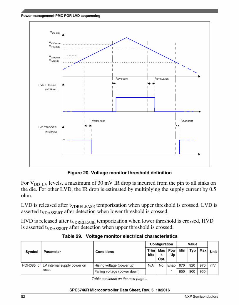
V
VV
V
DD_xxx
VLVD(fall)
HVD TRIGGER
LVD TRIGGER
VDRELEASE
LVD(rise)
t
t tVDASSERT
HVD(fall)
HVD(rise)
VDRELEASE
tVDASSERT
(INTERNAL)
(INTERNAL)
Figure 20. Voltage monitor threshold definition
For VDD_LV levels, a maximum of 30 mV IR drop is incurred from the pin to all sinks onthe die. For other LVD, the IR drop is estimated by multiplying the supply current by 0.5ohm.
LVD is released after tVDRELEASE temporization when upper threshold is crossed, LVD isasserted tVDASSERT after detection when lower threshold is crossed.
HVD is released after tVDRELEASE temporization when lower threshold is crossed, HVDis asserted tVDASSERT after detection when upper threshold is crossed.
Table 29. Voltage monitor electrical characteristics
Symbol Parameter Conditions
Configuration Value
UnitTrimbits
Mask
Opt.
Pow. Up
Min Typ Max
POR085_c1 LV internal supply power onreset
Rising voltage (power up) N/A No Enab.
870 920 970 mV
Falling voltage (power down) 850 900 950
Table continues on the next page...
Power management PMC POR LVD sequencing
SPC5746R Microcontroller Data Sheet, Rev. 5, 10/2016
52 NXP Semiconductors

Table 29. Voltage monitor electrical characteristics (continued)
Symbol Parameter Conditions
Configuration Value
UnitTrimbits
Mask
Opt.
Pow. Up
Min Typ Max
POR098_c LV internal supply power onreset
Rising voltage (power up) N/A No Enab.
960 1010 1060 mV
Falling voltage (power down) 940 990 1040
LVD_core_hot
LV internal2 supply low voltagemonitoring
Rising voltage (trimmed) 6bit No Enab.
1146 1169 1193 mV
Falling voltage (trimmed) 1146 1169 1193
LVD_core_cold
LV external3 supply low voltagemonitoring
Rising voltage 6bit Yes Disab.
1161 1185 1208 mV
Falling voltage 1161 1185 1208
HVD_core LV internal cold supply highvoltage monitoring
Rising voltage 6bit Yes Disab.
1353 1395 1438 mV
Falling voltage 1343 1385 1438
LVD_HV HV internal supply low voltagemonitoring
Rising voltage (trimmed) 6bit No Enab.
3300 3400 3500 mV
Falling voltage (trimmed) 3270 3370 3470
HVD_HV HV internal supply high voltagemonitoring
Rising voltage 6bit Yes Disab.
5530 5700 5870 mV
Falling voltage 5500 5670 5840
LVD_IO Main IO and RC oscillatorsupply voltage monitoring
Rising voltage (trimmed) 6bit No Enab.
3300 3400 3500 mV
Falling voltage (trimmed) 3270 3370 3470
LVD_SAR SAR ADC supply low voltagemonitoring
Rising voltage 6bit Yes Disab.
2820 2910 3000 mV
Falling voltage 2790 2880 2970
tVDASSERT Voltage detector thresholdcrossing assertion
— — — — 0.1 — 2.0 µs
tVDRELEASE Voltage detector thresholdcrossing de-assertion
— — — — 5 — 20 µs
1. POR085_c and POR096_c threshold are untrimmed value, before the completion of the power-up sequence. All otherLVD/HVD thresholds are provided after trimming.
2. LV internal supply levels are measured on device internal supply grid after internal voltage drop.3. LV external supply levels are measured on the die size of the package bond wire after package voltage drop.
16.1.6 Power up/down sequencingThe following shows the constraints and relationships for the different power supplies.
VDD_STDBY=0 VDD_LV=0 VDD_HV_PMC=0 VDD_HV_IO_MAIN=0 VDD_HV_IO_JTAG=0 VDD_HV_IO_FEC=0 VDD_HV_IO_MSC=0 VDD_HV_ADR_SD=0 VDD_HV_ADV_SD=0 VDD_HV_ADR_SAR=0 VDD_HV_ADV_SAR=0
VDD_STDBY VDD_LV VDD_HV_PMC VDD_HV_IO_MAIN VDD_HV_IO_JTAG VDD_HV_IO_FEC VDD_HV_IO_MSC VDD_HV_ADR_SD Amps VDD_HV_ADV_SD VDD_HV_ADR_SAR Amps VDD_HV_ADV_SAR 2mA
Figure 21. Device supply relation during power-up/power-down sequence
Power management PMC POR LVD sequencing
SPC5746R Microcontroller Data Sheet, Rev. 5, 10/2016
NXP Semiconductors 53

Each column indicates that the corresponding supply is 0 and the other supplies are UP.For example, the "Amps" cell in the "VDD_HV_ADV_SD=0" column shows that whenVDD_HV_ADR_SD supply is 0 and all other supplies are UP, this supply has a current inAmp flowing into VDD_HV_ADR_SD.
Flash memory specifications
17.1 Flash memory program and erase specifications
NOTEAll timing, voltage, and current numbers specified in thissection are defined for a single embedded flash memory withinan SoC, and represent average currents for given supplies andoperations.
Table 30 shows the estimated Program/Erase times.
Table 30. Flash memory program and erase specifications
Symbol Characteristic1 Typ2 FactoryProgramming3, 4
Field Update Unit
InitialMax
InitialMax, Full
Temp
TypicalEnd ofLife5
Lifetime Max6
20°C ≤TA≤30°C
-40°C ≤TJ≤150°C
-40°C ≤TJ≤150°C
≤ 1,000cycles
≤ 250,000cycles
tdwpgm Doubleword (64 bits) program time 43 100 150 55 500 μs
tppgm Page (256 bits) program time 73 200 300 108 500 μs
tqppgm Quad-page (1024 bits) programtime
268 800 1,200 396 2,000 μs
t16kers 16 KB Block erase time 168 290 320 250 1,000 ms
t16kpgm 16 KB Block program time 34 45 50 40 1,000 ms
t32kers 32 KB Block erase time 217 360 390 310 1,200 ms
t32kpgm 32 KB Block program time 69 100 110 90 1,200 ms
t64kers 64 KB Block erase time 315 490 590 420 1,600 ms
t64kpgm 64 KB Block program time 138 180 210 170 1,600 ms
t256kers 256 KB Block erase time 884 1,520 2,030 1,080 4,000 — ms
t256kpgm 256 KB Block program time 552 720 880 650 4,000 — ms
1. Program times are actual hardware programming times and do not include software overhead. Block program timesassume quad-page programming.
2. Typical program and erase times represent the median performance and assume nominal supply values and operation at25 °C. Typical program and erase times may be used for throughput calculations.
3. Conditions: ≤ 150 cycles, nominal voltage.4. Plant Programing times provide guidance for timeout limits used in the factory.
17
Flash memory specifications
SPC5746R Microcontroller Data Sheet, Rev. 5, 10/2016
54 NXP Semiconductors
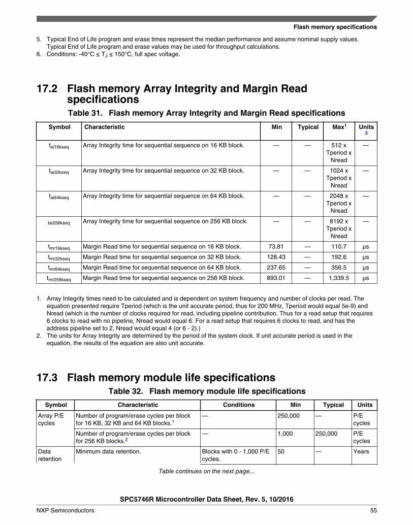
5. Typical End of Life program and erase times represent the median performance and assume nominal supply values.Typical End of Life program and erase values may be used for throughput calculations.
6. Conditions: -40°C ≤ TJ ≤ 150°C, full spec voltage.
17.2 Flash memory Array Integrity and Margin ReadspecificationsTable 31. Flash memory Array Integrity and Margin Read specifications
Symbol Characteristic Min Typical Max1 Units2
tai16kseq Array Integrity time for sequential sequence on 16 KB block. — — 512 xTperiod x
Nread
—
tai32kseq Array Integrity time for sequential sequence on 32 KB block. — — 1024 xTperiod x
Nread
—
tai64kseq Array Integrity time for sequential sequence on 64 KB block. — — 2048 xTperiod x
Nread
—
tai256kseq Array Integrity time for sequential sequence on 256 KB block. — — 8192 xTperiod x
Nread
—
tmr16kseq Margin Read time for sequential sequence on 16 KB block. 73.81 — 110.7 μs
tmr32kseq Margin Read time for sequential sequence on 32 KB block. 128.43 — 192.6 μs
tmr64kseq Margin Read time for sequential sequence on 64 KB block. 237.65 — 356.5 μs
tmr256kseq Margin Read time for sequential sequence on 256 KB block. 893.01 — 1,339.5 μs
1. Array Integrity times need to be calculated and is dependent on system frequency and number of clocks per read. Theequation presented require Tperiod (which is the unit accurate period, thus for 200 MHz, Tperiod would equal 5e-9) andNread (which is the number of clocks required for read, including pipeline contribution. Thus for a read setup that requires6 clocks to read with no pipeline, Nread would equal 6. For a read setup that requires 6 clocks to read, and has theaddress pipeline set to 2, Nread would equal 4 (or 6 - 2).)
2. The units for Array Integrity are determined by the period of the system clock. If unit accurate period is used in theequation, the results of the equation are also unit accurate.
17.3 Flash memory module life specificationsTable 32. Flash memory module life specifications
Symbol Characteristic Conditions Min Typical Units
Array P/Ecycles
Number of program/erase cycles per blockfor 16 KB, 32 KB and 64 KB blocks.1
— 250,000 — P/Ecycles
Number of program/erase cycles per blockfor 256 KB blocks.2
— 1,000 250,000 P/Ecycles
Dataretention
Minimum data retention. Blocks with 0 - 1,000 P/Ecycles.
50 — Years
Table continues on the next page...
Flash memory specifications
SPC5746R Microcontroller Data Sheet, Rev. 5, 10/2016
NXP Semiconductors 55

Table 32. Flash memory module life specifications (continued)
Symbol Characteristic Conditions Min Typical Units
Blocks with 100,000 P/Ecycles.
20 — Years
Blocks with 250,000 P/Ecycles.
10 — Years
1. Program and erase supported across standard temperature specs.2. Program and erase supported across standard temperature specs.
17.4 Data retention vs program/erase cycles
Graphically, Data Retention versus Program/Erase Cycles can be represented by thefollowing figure. The spec window represents qualified limits. The extrapolated dottedline demonstrates technology capability, however is beyond the qualification limits.
Flash memory specifications
SPC5746R Microcontroller Data Sheet, Rev. 5, 10/2016
56 NXP Semiconductors
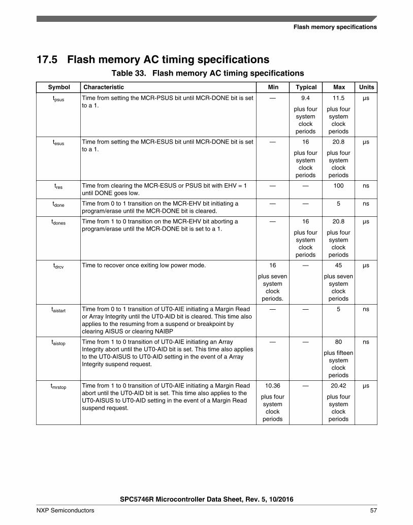
17.5 Flash memory AC timing specificationsTable 33. Flash memory AC timing specifications
Symbol Characteristic Min Typical Max Units
tpsus Time from setting the MCR-PSUS bit until MCR-DONE bit is setto a 1.
— 9.4
plus foursystemclock
periods
11.5
plus foursystemclock
periods
μs
tesus Time from setting the MCR-ESUS bit until MCR-DONE bit is setto a 1.
— 16
plus foursystemclock
periods
20.8
plus foursystemclock
periods
μs
tres Time from clearing the MCR-ESUS or PSUS bit with EHV = 1until DONE goes low.
— — 100 ns
tdone Time from 0 to 1 transition on the MCR-EHV bit initiating aprogram/erase until the MCR-DONE bit is cleared.
— — 5 ns
tdones Time from 1 to 0 transition on the MCR-EHV bit aborting aprogram/erase until the MCR-DONE bit is set to a 1.
— 16
plus foursystemclock
periods
20.8
plus foursystemclock
periods
μs
tdrcv Time to recover once exiting low power mode. 16
plus sevensystemclock
periods.
— 45
plus sevensystemclock
periods
μs
taistart Time from 0 to 1 transition of UT0-AIE initiating a Margin Reador Array Integrity until the UT0-AID bit is cleared. This time alsoapplies to the resuming from a suspend or breakpoint byclearing AISUS or clearing NAIBP
— — 5 ns
taistop Time from 1 to 0 transition of UT0-AIE initiating an ArrayIntegrity abort until the UT0-AID bit is set. This time also appliesto the UT0-AISUS to UT0-AID setting in the event of a ArrayIntegrity suspend request.
— — 80
plus fifteensystemclock
periods
ns
tmrstop Time from 1 to 0 transition of UT0-AIE initiating a Margin Readabort until the UT0-AID bit is set. This time also applies to theUT0-AISUS to UT0-AID setting in the event of a Margin Readsuspend request.
10.36
plus foursystemclock
periods
— 20.42
plus foursystemclock
periods
μs
Flash memory specifications
SPC5746R Microcontroller Data Sheet, Rev. 5, 10/2016
NXP Semiconductors 57
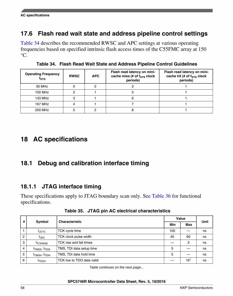
17.6 Flash read wait state and address pipeline control settings
Table 34 describes the recommended RWSC and APC settings at various operatingfrequencies based on specified intrinsic flash access times of the C55FMC array at 150°C.
Table 34. Flash Read Wait State and Address Pipeline Control Guidelines
Operating FrequencyfSYS
RWSC APCFlash read latency on mini-cache miss (# of fSYS clock
periods)
Flash read latency on mini-cache hit (# of fSYS clock
periods)
30 MHz 0 0 3 1
100 MHz 2 1 5 1
133 MHz 3 1 6 1
167 MHz 4 1 7 1
200 MHz 5 2 8 1
18 AC specifications
18.1 Debug and calibration interface timing
18.1.1 JTAG interface timing
These specifications apply to JTAG boundary scan only. See Table 36 for functionalspecifications.
Table 35. JTAG pin AC electrical characteristics
# Symbol CharacteristicValue
UnitMin Max
1 tJCYC TCK cycle time 100 — ns
2 tJDC TCK clock pulse width 40 60 ns
3 tTCKRISE TCK rise and fall times — 3 ns
4 tTMSS, tTDIS TMS, TDI data setup time 5 — ns
5 tTMSH, tTDIH TMS, TDI data hold time 5 — ns
6 tTDOV TCK low to TDO data valid — 161 ns
Table continues on the next page...
AC specifications
SPC5746R Microcontroller Data Sheet, Rev. 5, 10/2016
58 NXP Semiconductors
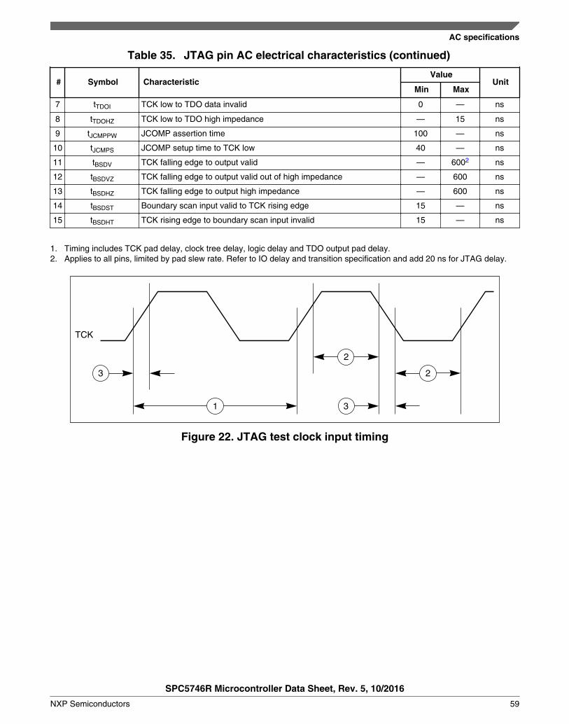
Table 35. JTAG pin AC electrical characteristics (continued)
# Symbol CharacteristicValue
UnitMin Max
7 tTDOI TCK low to TDO data invalid 0 — ns
8 tTDOHZ TCK low to TDO high impedance — 15 ns
9 tJCMPPW JCOMP assertion time 100 — ns
10 tJCMPS JCOMP setup time to TCK low 40 — ns
11 tBSDV TCK falling edge to output valid — 6002 ns
12 tBSDVZ TCK falling edge to output valid out of high impedance — 600 ns
13 tBSDHZ TCK falling edge to output high impedance — 600 ns
14 tBSDST Boundary scan input valid to TCK rising edge 15 — ns
15 tBSDHT TCK rising edge to boundary scan input invalid 15 — ns
1. Timing includes TCK pad delay, clock tree delay, logic delay and TDO output pad delay.2. Applies to all pins, limited by pad slew rate. Refer to IO delay and transition specification and add 20 ns for JTAG delay.
TCK
3
1 3
2
2
Figure 22. JTAG test clock input timing
AC specifications
SPC5746R Microcontroller Data Sheet, Rev. 5, 10/2016
NXP Semiconductors 59

TCK
6
87
5
TMS, TDI
TDO
4
Figure 23. JTAG test access port timing
TCK
JCOMP
9
10
Figure 24. JTAG JCOMP timing
AC specifications
SPC5746R Microcontroller Data Sheet, Rev. 5, 10/2016
60 NXP Semiconductors
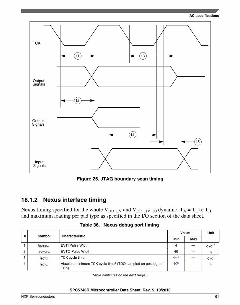
TCK
11
15
14
12
13
Output
Output
Input
Signals
Signals
Signals
Figure 25. JTAG boundary scan timing
18.1.2 Nexus interface timing
Nexus timing specified for the whole VDD_LV and VDD_HV_IO dynamic, TA = TL to TH,and maximum loading per pad type as specified in the I/O section of the data sheet.
Table 36. Nexus debug port timing
# Symbol CharacteristicValue Unit
Min Max
1 tEVTIPW EVTI Pulse Width 4 — tCYC, 1
2 tEVTOPW EVTO Pulse Width 40 — ns
3 tTCYC TCK cycle time 42, 3 — tCYC1
4 tTCYC Absolute minimum TCK cycle time4 (TDO sampled on posedge ofTCK)
405 — ns
Table continues on the next page...
AC specifications
SPC5746R Microcontroller Data Sheet, Rev. 5, 10/2016
NXP Semiconductors 61

Table 36. Nexus debug port timing (continued)
# Symbol CharacteristicValue Unit
Min Max
Absolute minimum TCK cycle time6 (TDO sampled on negedge ofTCK)
205 —
5 tNTDIS TDI data setup time 5 — ns
6 tNTDIH TDI data hold time 5 — ns
7 tNTMSS TMS data setup time 5 — ns
8 tNTMSH TMS data hold time 5 — ns
9 — TDO propagation delay from falling edge of TCK7 — 16 ns
10 — TDO hold time with respect to TCK falling edge (minimum TDOpropagation delay)
2.25 — ns
1. tCYC is system clock period.2. Achieving the absolute minimum TCK cycle time may require a maximum clock speed (system frequency / 8) that is less
than the maximum functional capability of the design (system frequency / 4) depending on the actual peripheral frequencybeing used. To ensure proper operation TCK frequency should be set to the peripheral frequency divided by a numbergreater than or equal to that specified here.
3. This is a functionally allowable feature. However, it may be limited by the maximum frequency specified by the Absoluteminimum TCK period specification.
4. This value is TDO propagation time 36ns + 4ns setup time to sampling edge.5. This may require a maximum clock speed (system frequency / 8) that is less than the maximum functional capability of the
design (system frequency / 4) depending on the actual system frequency being used.6. This value is TDO propagation time 16ns + 4ns setup time to sampling edge.7. Timing includes TCK pad delay, clock tree delay, logic delay and TDO output pad delay.
Figure 26. Nexus output timing
TCK
3
EVTIEVTO
Figure 27. Nexus event trigger and test clock timings
AC specifications
SPC5746R Microcontroller Data Sheet, Rev. 5, 10/2016
62 NXP Semiconductors

TCK
5
10
9
8
6
TMS, TDI
TDO
7
Figure 28. Nexus TDI, TMS, TDO timing
18.1.3 Aurora LVDS interface timingTable 37. Aurora LVDS interface timing specifications
Symbol ParameterValue
UnitMin Typ Max
Data Rate
— Data rate — 1250 Mbps
STARTUP
tSTRT_BIAS Bias startup time1 — — 5 µs
tSTRT_TX Transmitter startup time2 — — 5 µs
tSTRT_RX Receiver startup time3 — — 4 µs
1. Startup time is defined as the time taken by LVDS current reference block for settling bias current after its pwr_down(power down) has been deasserted. LVDS functionality is guaranteed only after the startup time.
2. Startup time is defined as the time taken by LVDS transmitter for settling after its pwr_down (power down) has beendeasserted. Here it is assumed that current reference is already stable (see Bias start-up time). LVDS functionality isguaranteed only after the startup time.
AC specifications
SPC5746R Microcontroller Data Sheet, Rev. 5, 10/2016
NXP Semiconductors 63

3. Startup time is defined as the time taken by LVDS receiver for settling after its pwr_down (power down) has beendeasserted. Here it is assumed that current reference is already stable (see Bias start-up time). LVDS functionality isguaranteed only after the startup time.
18.1.3.1 Aurora debug port timingTable 38. Aurora debug port timing
# Symbol ParameterValue
UnitMin Max
1 tREFCLK Reference clock frequency 625 1200 MHz
1a tMCYC Reference clock rise/fall time — 400 ps
2 tRCDC Reference clock duty cycle 45 55 %
3 JRC Reference clock jitter — 40 ps
4 tSTABILITY Reference clock stability 50 — PPM
5 BER Bit error rate — 10-12 —
6 JD Transmit lane deterministic jitter — 0.17 OUI
7 JT Transmit lane total jitter — 0.35 OUI
8 SO Differential output skew — 20 ps
9 SMO Lane to lane output skew — 1000 ps
10 OUI Aurora lane unit interval1 625 Mbps 1600 1600 ps
1.25Gbps 800 800 ps
1. ± 100 PPM
AC specifications
SPC5746R Microcontroller Data Sheet, Rev. 5, 10/2016
64 NXP Semiconductors

Tx Data [m]
Zero Crossover
CLOCKREF
CLOCKREF
1a
1
2
8
9 9
8 8
2
1a 1a 1a
Zero Crossover
Tx Data
Tx Data
Tx Data [n]
Ideal Zero Crossover
Zero Crossover
Tx Data [n+1]
Zero Crossover
Figure 29. Aurora timings
18.2 DSPI timing with CMOS and LVDS
DSPI in TSB mode with LVDS pads can be used to implement Micro Second Channelbus protocol.
DSPI channel frequency support is shown in Table 39. Timing specifications are shownin Table 40, Table 41, Table 42, Table 43, Table 44.
Table 39. DSPI channel frequency support
DSPI use modeMax usable frequency
(MHz)1,2
CMOS (Master mode) Full duplex – Classic timing (Table 40) 17
Full duplex – Modified timing (Table 41) 30
Output only mode (SCK/SOUT/PCS) (Table 40 and Table 41) 30
Output only mode TSB mode (SCK/SOUT/PCS) (Table 44) 30
LVDS (Master mode) Full duplex – Modified timing (Table 42) 40
AC specifications
SPC5746R Microcontroller Data Sheet, Rev. 5, 10/2016
NXP Semiconductors 65

1. Maximum usable frequency can be achieved if used with fastest configuration of the highest drive pads.2. Maximum usable frequency does not take into account external device propagation delay.
18.2.1 DSPI master mode full duplex timing with CMOS and LVDSpads
The values presented in these sections are target values. A complete performancecharacterization of the pads (in all configuration combinations) is required before thefinal specifications can be released.
18.2.1.1 DSPI CMOS master mode – classic timing
All output timing is worst case and includes the mismatching of rise and fall times of theoutput pads.
NOTEIn Table 40, all output timing is worst case and includes themismatching of rise and fall times of the output pads.
Table 40. DSPI CMOS master classic timing (full duplex and output only) - MTFE = 0, CPHA= 0 or 1
# Symbol Characteristic Condition Value1 Unit
Pad drive2 Load (CL) Min Max
1 tSCK SCK cycle time SCK drive strength
Very strong 25 pF 33.0 — ns
Strong 50 pF 80.0 —
Medium 50 pF 200.0 —
2 tCSC PCS to SCK delay SCK and PCS drive strength
Very strong 25 pF (N3 x tSYS, 4) - 16 — ns
Strong 50 pF (N3 x tSYS, 4) - 16 —
Medium 50 pF (N3 x tSYS, 4) - 16 —
PCS medium andSCK strong
PCS = 50 pF
SCK = 50 pF
(N3 x tSYS, 4) - 29 —
3 tASC After SCK delay SCK and PCS drive strength
Very strong PCS = 0 pF
SCK = 50 pF
(M5 x tSYS4) - 35 — ns
Strong PCS = 0 pF
SCK = 50 pF
(M5 x tSYS, 4) - 35 —
Medium PCS = 0 pF
SCK = 50 pF
(M5 x tSYS, 4) - 35 —
PCS medium andSCK strong
PCS = 0 pF (M5 x tSYS, 4) - 35 —
Table continues on the next page...
AC specifications
SPC5746R Microcontroller Data Sheet, Rev. 5, 10/2016
66 NXP Semiconductors

Table 40. DSPI CMOS master classic timing (full duplex and output only) - MTFE = 0, CPHA= 0 or 1 (continued)
# Symbol Characteristic Condition Value1 Unit
Pad drive2 Load (CL) Min Max
SCK = 50 pF
4 tSDC SCK duty cycle6 SCK drive strength
Very strong 0 to 50 pF 1/2tSCK - 2 1/2tSCK + 2 ns
Strong 0 to 50 pF 1/2tSCK - 2 1/2tSCK + 2
Medium 0 to 50 pF 1/2tSCK - 5 1/2tSCK + 5
PCS strobe timing
5 tPCSC PCSx to PCSS time,
7PCS and PCSS drive strength
Strong 25 pF 13.0 — ns
6 tPASC PCSS to PCSx time7 PCS and PCSS drive strength
Strong 25 pF 13.0 — ns
SIN setup time
7 tSUI SIN setup time toSCK8
SCK drive strength
Very strong 25 pF 25.0 — ns
Strong 50 pF 31.0 —
Medium 50 pF 52.0 —
SIN hold time
8 tHI SIN hold time fromSCK8
SCK drive strength
Very strong 0 pF -1.0 — ns
Strong 0 pF -1.0 —
Medium 0 pF -1.0 —
SOUT data valid time (after SCK edge)
9 tSUO SOUT data valid timefrom SCK9
SOUT and SCK drive strength
Very strong 25 pF — 7.0 ns
Strong 50 pF — 8.0
Medium 50 pF — 16.0
SOUT data hold time (after SCK edge)
10 tHO SOUT data hold timeafter SCK9
SOUT and SCK drive strength
Very strong 25 pF -7.7 — ns
Strong 50 pF -11.0 —
Medium 50 pF -15.0 —
1. All timing values for output signals in this table are measured to 50% of the output voltage.2. Timing is guaranteed to same drive capabilities for all signals, mixing of pad drives may reduce operating speeds and may
cause incorrect operation.3. N is the number of clock cycles added to time between PCS assertion and SCK assertion and is software programmable
using DSPI_CTARx[PSSCK] and DSPI_CTARx[CSSCK]. The minimum value is 2 cycles unless TSB mode or ContinuousSCK clock mode is selected, in which case, N is automatically set to 0 clock cycles (PCS and SCK are driven by the sameedge of DSPI_CLKn).
4. tSYS is the period of DSPI_CLKn clock, the input clock to the DSPI module. Maximum frequency is 100 MHz (min tSYS = 10ns).
AC specifications
SPC5746R Microcontroller Data Sheet, Rev. 5, 10/2016
NXP Semiconductors 67

5. M is the number of clock cycles added to time between SCK negation and PCS negation and is software programmableusing DSPI_CTARx[PASC] and DSPI_CTARx[ASC]. The minimum value is 2 cycles unless TSB mode or Continuous SCKclock mode is selected, in which case, M is automatically set to 0 clock cycles (PCS and SCK are driven by the same edgeof DSPI_CLKn).
6. tSDC is only valid for even divide ratios. For odd divide ratios the fundamental duty cycle is not 50:50. For these odd divideratios cases, the absolute spec number is applied as jitter/uncertainty to the nominal high time and low time.
7. PCSx and PCSS using same pad configuration.8. Input timing assumes an input slew rate of 1 ns (10% - 90%) and uses TTL voltage thresholds.9. SOUT Data Valid and Data hold are independent of load capacitance if SCK and SOUT load capacitances are the same
value.
Data
Data Last DataFirst Data
First Data Last DataSIN
SOUT
SCK Output
SCK OutputSCK Output(CPOL = 0)
PCSx
(CPOL = 1)
tSCKtSDC
tSDC
CSC ttASC
tt
SUIHI
tSUO tHO
Figure 30. DSPI CMOS master mode – classic timing, CPHA = 0
AC specifications
SPC5746R Microcontroller Data Sheet, Rev. 5, 10/2016
68 NXP Semiconductors

SCK Output
SIN
SOUT Fist Data
Fist Data
Last Data
Last Data
Data
Data
SCK Output(CPOL = 0)
PCSx
(CPOL = 1)
t t
t t
SUI HI
SUO HO
Figure 31. DSPI CMOS master mode – classic timing, CPHA = 1
PCSx
PCSS
tPCSC tPASC
Figure 32. DSPI PCS strobe (PCSS) timing (master mode)
18.2.1.2 DSPI CMOS master mode – modified timing
All output timing is worst case and includes the mismatching of rise and fall times of theoutput pads.
NOTEIn Table 41, all output timing is worst case and includes themismatching of rise and fall times of the output pads.
Table 41. DSPI CMOS master modified timing (full duplex and output only) - MTFE = 1,CPHA = 0 or 1
# Symbol Characteristic Condition Value1 Unit
Pad drive2 Load (CL) Min Max
1 tSCK SCK cycle time SCK drive strength
Very strong 25 pF 33.0 — ns
Strong 50 pF 80.0 —
Table continues on the next page...
AC specifications
SPC5746R Microcontroller Data Sheet, Rev. 5, 10/2016
NXP Semiconductors 69

Table 41. DSPI CMOS master modified timing (full duplex and output only) - MTFE = 1,CPHA = 0 or 1 (continued)
# Symbol Characteristic Condition Value1 Unit
Pad drive2 Load (CL) Min Max
Medium 50 pF 200.0 —
2 tCSC PCS to SCK delay SCK and PCS drive strength
Very strong 25 pF (N3 x tSYS, 4) - 16 — ns
Strong 50 pF (N3 x tSYS, 4) - 16 —
Medium 50 pF (N3 x tSYS, 4) - 16 —
PCS medium andSCK strong
PCS = 50 pF
SCK = 50 pF
(N3 x tSYS, 4) - 29 —
3 tASC After SCK delay SCK and PCS drive strength
Very strong PCS = 0 pF
SCK = 50 pF
(M5 x tSYS4) - 35 — ns
Strong PCS = 0 pF
SCK = 50 pF
(M5 x tSYS, 4) - 35 —
Medium PCS = 0 pF
SCK = 50 pF
(M5 x tSYS, 4) - 35 —
PCS medium andSCK strong
PCS = 0 pF
SCK = 50 pF
(M5 x tSYS, 4) - 35 —
4 tSDC SCK duty cycle6 SCK drive strength
Very strong 0 to 50 pF 1/2tSCK - 2 1/2tSCK + 2 ns
Strong 0 to 50 pF 1/2tSCK - 2 1/2tSCK + 2
Medium 0 to 50 pF 1/2tSCK - 5 1/2tSCK + 5
PCS strobe timing
5 tPCSC PCSx to PCSS time,
7PCS and PCSS drive strength
Strong 25 pF 13.0 — ns
6 tPASC PCSS to PCSx time7 PCS and PCSS drive strength
Strong 25 pF 13.0 — ns
SIN setup time
7 tSUI SIN setup time toSCK
CPHA = 08
SCK drive strength
Very strong 25 pF 25 - (P9 x tSYS4) — ns
Strong 50 pF 31 - (P9 x tSYS, 4) —
Medium 50 pF 52 - (P9 x tSYS, 4) —
SIN setup time toSCK
CPHA = 18
SCK drive strength
Very strong 25 pF 25.0 — ns
Strong 50 pF 31.0 —
Medium 50 pF 52.0 —
SIN hold time
8 tHI SIN hold time fromSCK
SCK drive strength
Very strong 0 pF -1 + (P8 x tSYS, 3) — ns
Table continues on the next page...
AC specifications
SPC5746R Microcontroller Data Sheet, Rev. 5, 10/2016
70 NXP Semiconductors

Table 41. DSPI CMOS master modified timing (full duplex and output only) - MTFE = 1,CPHA = 0 or 1 (continued)
# Symbol Characteristic Condition Value1 Unit
Pad drive2 Load (CL) Min Max
CPHA = 09 Strong 0 pF -1 + (P8 x tSYS, 3) —
Medium 0 pF -1 + (P8 x tSYS, 3) —
SIN hold time fromSCK CPHA = 19
SCK drive strength
Very strong 0 pF -1.0 — ns
Strong 0 pF -1.0 —
Medium 0 pF -1.0 —
SOUT data valid time (after SCK edge)
9 tSUO SOUT data valid timefrom SCK
CPHA = 09
SOUT and SCK drive strength
Very strong 25 pF — 7.0 + tSYS4 ns
Strong 50 pF — 8.0 + tSYS4
Medium 50 pF — 16.0 + tSYS4
SOUT data valid timefrom SCK
CPHA = 19
SOUT and SCK drive strength
Very strong 25 pF — 7.0 ns
Strong 50 pF — 8.0
Medium 50 pF — 16.0
SOUT data hold time (after SCK edge)
10 tHO SOUT data hold timeafter SCK
CPHA = 010
SOUT and SCK drive strength
Very strong 25 pF -7.7 + tSYS4 — ns
Strong 50 pF -11.0 + tSYS4 —
Medium 50 pF -15.0 + tSYS4 —
SOUT data hold timeafter SCK
CPHA = 110
SOUT and SCK drive strength
Very strong 25 pF -7.7 — ns
Strong 50 pF -11.0 —
Medium 50 pF -15.0 —
1. All timing values for output signals in this table are measured to 50% of the output voltage.2. Timing is guaranteed to same drive capabilities for all signals, mixing of pad drives may reduce operating speeds and may
cause incorrect operation.3. N is the number of clock cycles added to time between PCS assertion and SCK assertion and is software programmable
using DSPI_CTARx[PSSCK] and DSPI_CTARx[CSSCK]. The minimum value is 2 cycles unless TSB mode or ContinuousSCK clock mode is selected, in which case, N is automatically set to 0 clock cycles (PCS and SCK are driven by the sameedge of DSPI_CLKn).
4. tSYS is the period of DSPI_CLKn clock, the input clock to the DSPI module. Maximum frequency is 100 MHz (min tSYS = 10ns).
5. M is the number of clock cycles added to time between SCK negation and PCS negation and is software programmableusing DSPI_CTARx[PASC] and DSPI_CTARx[ASC]. The minimum value is 2 cycles unless TSB mode or Continuous SCKclock mode is selected, in which case, M is automatically set to 0 clock cycles (PCS and SCK are driven by the same edgeof DSPI_CLKn).
6. tSDC is only valid for even divide ratios. For odd divide ratios the fundamental duty cycle is not 50:50. For these odd divideratios cases, the absolute spec number is applied as jitter/uncertainty to the nominal high time and low time.
7. PCSx and PCSS using same pad configuration.8. Input timing assumes an input slew rate of 1 ns (10% - 90%) and uses TTL voltage thresholds.
AC specifications
SPC5746R Microcontroller Data Sheet, Rev. 5, 10/2016
NXP Semiconductors 71

9. P is the number of clock cycles added to delay the DSPI input sample point and is software programmable usingDSPI_MCR[SMPL_PT]. The value must be 0, 1 or 2. If the baud rate divide ratio is /2 or /3, this value is automatically setto 1.
10. SOUT Data Valid and Data hold are independent of load capacitance if SCK and SOUT load capacitances are the samevalue.
Data
Data Last DataFirst Data
First Data Last DataSIN
SOUT
SCK Output
SCK Output(CPOL = 0)
PCSx
(CPOL = 1)
tSCKtSDC
tSDC
CSC ttASC
tt
SUIHI
tSUO tHO
Figure 33. DSPI CMOS master mode – modified timing, CPHA = 0
SIN
PCSx
SCK Output
SCK Output
SOUT First Data
First Data
(CPOL=1)
(CPOL=0)
Last Data
Last Data
DataData
Data
tSUI tHI
tSUO tHO
tHI
Figure 34. DSPI CMOS master mode – modified timing, CPHA = 1
AC specifications
SPC5746R Microcontroller Data Sheet, Rev. 5, 10/2016
72 NXP Semiconductors
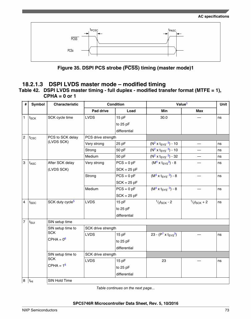
PCSx
PCSS
tPCSC tPASC
Figure 35. DSPI PCS strobe (PCSS) timing (master mode)1
18.2.1.3 DSPI LVDS master mode – modified timingTable 42. DSPI LVDS master timing - full duplex - modified transfer format (MTFE = 1),
CPHA = 0 or 1
# Symbol Characteristic Condition Value1 Unit
Pad drive Load Min Max
1 tSCK SCK cycle time LVDS 15 pF
to 25 pF
differential
30.0 — ns
2 tCSC PCS to SCK delay(LVDS SCK)
PCS drive strength
Very strong 25 pF (N2 x tSYS, 3) - 10 — ns
Strong 50 pF (N2 x tSYS, 3) - 10 — ns
Medium 50 pF (N2 x tSYS, 3) - 32 — ns
3 tASC After SCK delay
(LVDS SCK)
Very strong PCS = 0 pF
SCK = 25 pF
(M4 x tSYS3) - 8 — ns
Strong PCS = 0 pF
SCK = 25 pF
(M4 x tSYS, 3) - 8 — ns
Medium PCS = 0 pF
SCK = 25 pF
(M4 x tSYS, 3) - 8 — ns
4 tSDC SCK duty cycle5 LVDS 15 pF
to 25 pF
differential
1/2tSCK - 2 1/2tSCK + 2 ns
7 tSUI SIN setup time
SIN setup time toSCK
CPHA = 06
SCK drive strength
LVDS 15 pF
to 25 pF
differential
23 - (P7 x tSYS3) — ns
SIN setup time toSCK
CPHA = 16
SCK drive strength
LVDS 15 pF
to 25 pF
differential
23 — ns
8 tHI SIN Hold Time
Table continues on the next page...
AC specifications
SPC5746R Microcontroller Data Sheet, Rev. 5, 10/2016
NXP Semiconductors 73

Table 42. DSPI LVDS master timing - full duplex - modified transfer format (MTFE = 1),CPHA = 0 or 1 (continued)
# Symbol Characteristic Condition Value1 Unit
Pad drive Load Min Max
SIN hold time fromSCK
CPHA = 06
SCK drive strength
LVDS 0 pF differential -1 + (P7 x tSYS, 3) — ns
SIN hold time fromSCK
CPHA = 16
SCK drive strength
LVDS 0 pF differential -1 — ns
9 tSUO SOUT data valid time (after SCK edge)
SOUT data valid timefrom SCK
CPHA = 08
SOUT and SCK drive strength
LVDS 15 pF
to 25 pF
differential
— 7.0 + tSYS3 ns
SOUT data valid timefrom SCK
CPHA = 18
SOUT and SCK drive strength
LVDS 15 pF
to 25 pF
differential
— 7.0 ns
10 tHO SOUT data hold time (after SCK edge)
SOUT data hold timeafter SCK
CPHA = 08
SOUT and SCK drive strength
LVDS 15 pF
to 25 pF
differential
-7.5 + tSYS3 — ns
SOUT data hold timeafter SCK
CPHA = 18
SOUT and SCK drive strength
LVDS 15 pF
to 25 pF
differential
-7.5 — ns
1. All timing values for output signals in this table are measured to 50% of the output voltage.2. N is the number of clock cycles added to time between PCS assertion and SCK assertion and is software programmable
using DSPI_CTARx[PSSCK] and DSPI_CTARx[CSSCK]. The minimum value is 2 cycles unless TSB mode or ContinuousSCK clock mode is selected, in which case, N is automatically set to 0 clock cycles (PCS and SCK are driven by the sameedge of DSPI_CLKn).
3. tSYS is the period of DSPI_CLKn clock, the input clock to the DSPI module. Maximum frequency is 100 MHz (min tSYS = 10ns).
4. M is the number of clock cycles added to time between SCK negation and PCS negation and is software programmableusing DSPI_CTARx[PASC] and DSPI_CTARx[ASC]. The minimum value is 2 cycles unless TSB mode or Continuous SCKclock mode is selected, in which case, M is automatically set to 0 clock cycles (PCS and SCK are driven by the same edgeof DSPI_CLKn).
5. tSDC is only valid for even divide ratios. For odd divide ratios the fundamental duty cycle is not 50:50. For these odd divideratios cases, the absolute spec number is applied as jitter/uncertainty to the nominal high time and low time.
6. Input timing assumes an input slew rate of 1 ns (10% - 90%) and LVDS differential voltage = ±100 mV.7. P is the number of clock cycles added to delay the DSPI input sample point and is software programmable using
DSPI_MCR[SMPL_PT]. The value must be 0, 1 or 2. If the baud rate divide ratio is /2 or /3, this value is automatically setto 1.
8. SOUT Data Valid and Data hold are independent of load capacitance if SCK and SOUT load capacitances are the samevalue.
AC specifications
SPC5746R Microcontroller Data Sheet, Rev. 5, 10/2016
74 NXP Semiconductors

Data
Data Last DataFirst Data
First Data Last DataSIN
SOUT
SCK Output
SCK OutputSCK Output(CPOL = 0)
PCSx
(CPOL = 1)
tSCKtSDC
tSDC
CSC ttASC
tt
SUIHI
tSUO tHO
Figure 36. DSPI LVDS master mode – modified timing, CPHA = 0
DataFirst Data
First Data Last DataData
Last DataSIN
PCSx
SCK Output
SCK Output
(CPOL = 0)
(CPOL = 1)
SOUT
tSUI t tHI HI
tSUO tHO
Figure 37. DSPI LVDS master mode – modified timing, CPHA = 1
18.2.1.4 DSPI master mode – output only
For Table 43 :
AC specifications
SPC5746R Microcontroller Data Sheet, Rev. 5, 10/2016
NXP Semiconductors 75

• All DSPI timing specifications apply to pins when using LVDS pads for SCK andSOUT and CMOS pad for PCS with pad driver strength as defined. Timing maydegrade for weaker output drivers.
• TSB = 1 or ITSB = 1 automatically selects MTFE = 1 and CPHA = 1.
Table 43. DSPI LVDS master timing - output only - timed serial bus mode TSB = 1 or ITSB =1, CPOL = 0 or 1, continuous SCK clock
# Symbol Characteristic Condition Value Unit
Pad drive Load Min Max
1 tSCK SCK cycle time LVDS 15 pF
to 50 pF
differential
25.0 — ns
2 tCSV PCS valid after SCK1
(SCK with 50 pFdifferential load cap.)
Very strong 25 pF — 6.0 ns
Strong 50 pF — 6.0 ns
3 tCSH PCS hold after SCK1
(SCK with 50 pFdifferential load cap.)
Very strong 0 pF -4.0 — ns
Strong 0 pF -4.0 — ns
4 tSDC SCK duty cycle
(SCK with 50 pFdifferential load cap.)
LVDS 15 pF
to 50 pF
differential
1/2tSCK - 2 1/2tSCK + 2 ns
SOUT data valid time (after SCK edge)
5 tSUO SOUT data valid timefrom SCK2
SOUT and SCK drive strength
LVDS 15 pF
to 50 pF
differential
— 3.5 ns
SOUT data hold time (after SCK edge)
6 tHO SOUT data hold timeafter SCK2
SOUT and SCK drive strength
LVDS 15 pF
to 50 pF
differential
-3.5 — ns
1. With TSB mode or Continuous SCK clock mode selected, PCS and SCK are driven by the same edge of DSPI_CLKn. Thistiming value is due to pad delays and signal propagation delays.
2. SOUT Data Valid and Data hold are independent of load capacitance if SCK and SOUT load capacitances are the samevalue.
For Table 44 :
• TSB = 1 or ITSB = 1 automatically selects MTFE = 1 and CPHA = 1.• All output timing is worst case and includes the mismatching of rise and fall times of
the output pads.
AC specifications
SPC5746R Microcontroller Data Sheet, Rev. 5, 10/2016
76 NXP Semiconductors

Table 44. DSPI CMOS master timing - output only - timed serial bus mode TSB = 1 or ITSB =1, CPOL = 0 or 1, continuous SCK clock
# Symbol Characteristic Condition Value1 Unit
Pad drive2 Load (CL) Min Max
1 tSCK SCK cycle time SCK drive strength
Very strong 25 pF 33.0 — ns
Strong 50 pF 80.0 — ns
Medium 50 pF 200.0 — ns
2 tCSV PCS valid after SCK3 SCK and PCS drive strength
Very strong 25 pF 7 — ns
Strong 50 pF 8 — ns
Medium 50 pF 16 — ns
PCS medium andSCK strong
PCS = 50 pF
SCK = 50 pF
29 — ns
3 tCSH PCS hold after SCK3 SCK and PCS drive strength
Very strong PCS = 0 pF
SCK = 50 pF
-14 — ns
Strong PCS = 0 pF
SCK = 50 pF
-14 — ns
Medium PCS = 0 pF
SCK = 50 pF
-33 — ns
PCS medium andSCK strong
PCS = 0 pF
SCK = 50 pF
-35 — ns
4 tSDC SCK duty cycle4 SCK drive strength
Very strong 0 to 50 pF 1/2tSCK - 2 1/2tSCK + 2 ns
Strong 0 to 50 pF 1/2tSCK - 2 1/2tSCK + 2 ns
Medium 0 to 50 pF 1/2tSCK - 5 1/2tSCK + 5 ns
SOUT data valid time (after SCK edge)
9 tSUO SOUT data valid timefrom SCK
CPHA = 1, 5
SOUT and SCK drive strength
Very strong 25 pF — 7.0 ns
Strong 50 pF — 8.0 ns
Medium 50 pF — 16.0 ns
SOUT data hold time (after SCK edge)
10 tHO SOUT data hold timeafter SCK CPHA = 15
SOUT and SCK drive strength
Very strong 25 pF -7.7 — ns
Strong 50 pF -11.0 — ns
Medium 50 pF -15.0 — ns
1. All timing values for output signals in this table are measured to 50% of the output voltage.2. Timing is guaranteed to same drive capabilities for all signals, mixing of pad drives may reduce operating speeds and may
cause incorrect operation.3. With TSB mode or Continuous SCK clock mode selected, PCS and SCK are driven by the same edge of DSPI_CLKn. This
timing value is due to pad delays and signal propagation delays.
AC specifications
SPC5746R Microcontroller Data Sheet, Rev. 5, 10/2016
NXP Semiconductors 77

4. tSDC is only valid for even divide ratios. For odd divide ratios the fundamental duty cycle is not 50:50. For these odd divideratios cases, the absolute spec number is applied as jitter/uncertainty to the nominal high time and low time.
5. SOUT Data Valid and Data hold are independent of load capacitance if SCK and SOUT load capacitances are the samevalue.
PCSx
SCK Output(CPOL = 0)
SOUT First Data Last DataData
tSUO tHO
tCSV tSDC tSCK tCSH
Figure 38. DSPI LVDS and CMOS master timing – output only – modified transfer formatMTFE = 1, CHPA = 1
18.2.2 DSPI CMOS slave mode
NOTEDSPI slave operation is only supported for a single master andsingle slave on the device. Timing is valid for that case only.
Table 45. DSPI CMOS slave timing - Modified Transfer Format (MTFE = 0/1)
# Symbol Characteristic1 Condition Value Unit
Pad drive Load Min Max
1 tSCK SCK Cycle Time — — 62 — ns
2 tCSC SS to SCK Delay — — 16 — ns
3 tASC SCK to SS Delay — — 16 — ns
4 tSDC SCK Duty Cycle — — 30 — ns
5 tA Slave Access Time2
(SS active to SOUTdriven)
Very strong 25 pF — 50 ns
Strong 50 pF — 50 ns
Medium 50 pF — 60 ns
6 tDIS Slave SOUT DisableTime2
(SS inactive to SOUTHigh-Z or invalid)
Very strong 25 pF — 5 ns
Strong 50 pF — 5 ns
Medium 50 pF — 10 ns
9 tSUI Data Setup Time forInputs
— — 10 — ns
Table continues on the next page...
AC specifications
SPC5746R Microcontroller Data Sheet, Rev. 5, 10/2016
78 NXP Semiconductors

Table 45. DSPI CMOS slave timing - Modified Transfer Format (MTFE = 0/1) (continued)
# Symbol Characteristic1 Condition Value Unit
Pad drive Load Min Max
10 tHI Data Hold Time forInputs
— — 10 — ns
11 tSUO SOUT Valid Time2
(after SCK edge)
Very strong 25 pF — 30 ns
Strong 50 pF — 30 ns
Medium 50 pF — 50 ns
12 tHO SOUT Hold Time2
(after SCK edge)
Very strong 25 pF 2.5 — ns
Strong 50 pF 2.5 — ns
Medium 50 pF 2.5 — ns
1. Input timing assumes an input slew rate of 1 ns (10% - 90%) and uses TTL / Automotive voltage thresholds.2. All timing values for output signals in this table, are measured to 50% of the output voltage. All output timing is worst case
and includes the mismatching of rise and fall times of the output pads.
L a s t D a ta F irs t D a ta
D a ta
D a ta
S IN
S O U T
S S
S C K In p u t
F irs t D a ta L a s t D a ta
S C K In p u t
(C P O L = 0 )
(C P O L = 1 )
tSCK
tAtDIS
tSDC
tSDC
tCSCtASC
tSUI tHI
tSUO tHO
Figure 39. DSPI Slave Mode - Modified transfer format timing (MFTE = 0/1) — CPHA = 0
AC specifications
SPC5746R Microcontroller Data Sheet, Rev. 5, 10/2016
NXP Semiconductors 79
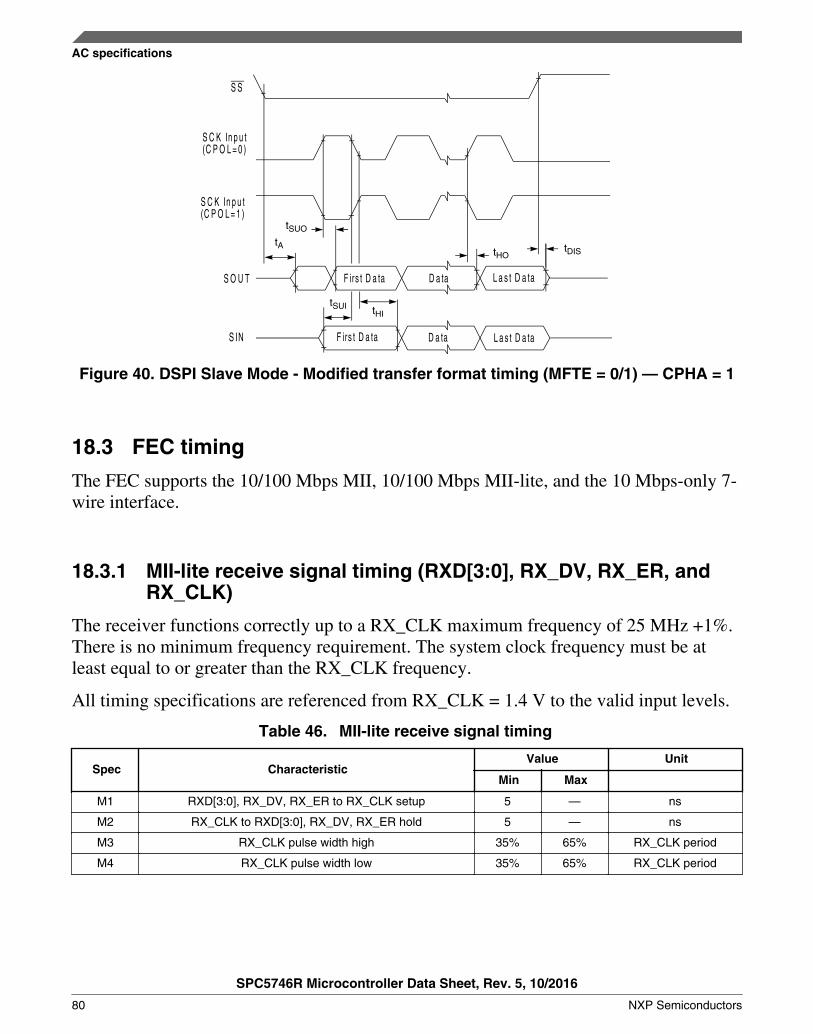
L a s t D a ta
L a s t D a taS IN
S O U T
S S
F irs t D a ta
F irs t D a ta
D a ta
D a ta
S C K In p u t
S C K In p u t
(C P O L = 0 )
(C P O L = 1 )
tA tDIS
tSUI tHI
tSUO
tHO
Figure 40. DSPI Slave Mode - Modified transfer format timing (MFTE = 0/1) — CPHA = 1
18.3 FEC timing
The FEC supports the 10/100 Mbps MII, 10/100 Mbps MII-lite, and the 10 Mbps-only 7-wire interface.
18.3.1 MII-lite receive signal timing (RXD[3:0], RX_DV, RX_ER, andRX_CLK)
The receiver functions correctly up to a RX_CLK maximum frequency of 25 MHz +1%.There is no minimum frequency requirement. The system clock frequency must be atleast equal to or greater than the RX_CLK frequency.
All timing specifications are referenced from RX_CLK = 1.4 V to the valid input levels.
Table 46. MII-lite receive signal timing
Spec CharacteristicValue Unit
Min Max
M1 RXD[3:0], RX_DV, RX_ER to RX_CLK setup 5 — ns
M2 RX_CLK to RXD[3:0], RX_DV, RX_ER hold 5 — ns
M3 RX_CLK pulse width high 35% 65% RX_CLK period
M4 RX_CLK pulse width low 35% 65% RX_CLK period
AC specifications
SPC5746R Microcontroller Data Sheet, Rev. 5, 10/2016
80 NXP Semiconductors

M3
M4
M1
RX_CLK (input)
RXD[3:0] (inputs)RX_DVRX_ER
M2
Figure 41. MII-lite receive signal timing diagram
18.3.2 MII-lite transmit signal timing (TXD[3:0], TX_EN, TX_ER,TX_CLK)
The transmitter functions correctly up to a TX_CLK maximum frequency of 25 MHz+1%. There is no minimum frequency requirement. The system clock frequency must beat least equal to or greater than the TX_CLK frequency.
The transmit outputs (TXD[3:0], TX_EN, TX_ER) can be programmed to transition fromeither the rising or falling edge of TX_CLK, and the timing is the same in either case.This options allows the use of non-compliant MII PHYs.
All timing specifications are referenced from TX_CLK = 1.4 V to the valid output levels.
Table 47. MII-lite transmit signal timing
Spec CharacteristicValue1 Unit
Min Max
M5 TX_CLK to TXD[3:0], TX_EN, TX_ER invalid 5 — ns
M6 TX_CLK to TXD[3:0], TX_EN, TX_ER valid — 25 ns
M7 TX_CLK pulse width high 35% 65% TX_CLK period
M8 TX_CLK pulse width low 35% 65% TX_CLK period
1. Output parameters are valid for CL = 25 pF, where CL is the external load to the device. The internal package capacitanceis accounted for, and does not need to be subtracted from the 25 pF value.
AC specifications
SPC5746R Microcontroller Data Sheet, Rev. 5, 10/2016
NXP Semiconductors 81

M5
M8
M7
M6
TX_CLK (input)
TXD[3:0] (outputs)TX_ENTX_ER
Figure 42. MII-lite transmit signal timing diagram
18.3.3 MII-lite async inputs signal timing (CRS and COL)
Table 48. MII-lite async inputs signal timing
Spec CharacteristicValue Unit
Min Max
M9 CRS, COL minimum pulse width 1.5 — TX_CLK period
CRS, COL
M9
Figure 43. MII-lite async inputs timing diagram
18.3.4 MII-lite serial management channel timing (MDIO and MDC)
The FEC functions correctly with a maximum MDC frequency of 2.5 MHz.
NOTEAll timing specifications are referenced from MDC = 1.4 V(TTL levels) to the valid input and output levels, 0.8 V and 2.0V (TTL levels). For 5 V operation, timing is referenced fromMDC = 50% to 2.2 V/3.5 V input and output levels.
AC specifications
SPC5746R Microcontroller Data Sheet, Rev. 5, 10/2016
82 NXP Semiconductors

Table 49. MII-lite serial management channel timing
Spec CharacteristicValue Unit
Min Max
M10 MDC falling edge to MDIO output invalid (minimumpropagation delay)
0 — ns
M11 MDC falling edge to MDIO output valid (max prop delay) — 25 ns
M12 MDIO (input) to MDC rising edge setup 10 — ns
M13 MDIO (input) to MDC rising edge hold 0 — ns
M14 MDC pulse width high 40% 60% MDC period
M15 MDC pulse width low 40% 60% MDC period
M11
M10
MDC (output)
MDIO (output)
M12M13
MDIO (input)
M14 M15
Figure 44. MII-lite serial management channel timing diagram
18.3.5 RMII serial management channel timing (MDIO and MDC)
The FEC functions correctly with a maximum MDC frequency of 2.5 MHz.
Table 50. RMII serial management channel timing
Spec CharacteristicValue Unit
Min Max
M10 MDC falling edge toMDIO output invalid
(minimum propagationdelay)
0 — ns
Table continues on the next page...
AC specifications
SPC5746R Microcontroller Data Sheet, Rev. 5, 10/2016
NXP Semiconductors 83

Table 50. RMII serial management channel timing (continued)
Spec CharacteristicValue Unit
Min Max
M11 MDC falling edge toMDIO output valid (max
prop delay)
— 25 ns
M12 MDIO (input) to MDCrising edge setup
10 — ns
M13 MDIO (input) to MDCrising edge hold
0 — ns
M14 MDC pulse width high 40% 60% MDC period
M15 MDC pulse width low 40% 60% MDC period
MDC (output)
MDIO (output)
MDIO (input)
M12M13
M10
M15M14
M11
Figure 45. RMII-lite serial management channel timing diagram
18.3.6 RMII receive signal timing (RXD[1:0], CRS_DV)
The receiver functions correctly up to a REF_CLK maximum frequency of 50 MHz +1%.There is no minimum frequency requirement. The system clock frequency must be atleast equal to or greater than the RX_CLK frequency, which is half that of the REF_CLKfrequency.
All timing specifications are referenced from REF_CLK = 1.4 V to the valid input levels.
AC specifications
SPC5746R Microcontroller Data Sheet, Rev. 5, 10/2016
84 NXP Semiconductors

Table 51. RMII receive signal timing
Spec CharacteristicValue Unit
Min Max
R1 RXD[1:0], CRS_DV to REF_CLK setup 4 — ns
R2 REF_CLK to RXD[1:0], CRS_DV hold 2 — ns
R3 REF_CLK pulse width high 35% 65% REF_CLK period
R4 REF_CLK pulse width low 35% 65% REF_CLK period
R2R1
REF_CLK (input)
RXD[1:0] (inputs)CRS_DV
R3
R4
Figure 46. RMII receive signal timing diagram
18.3.7 RMII transmit signal timing (TXD[1:0], TX_EN)
The transmitter functions correctly up to a REF_CLK maximum frequency of 50 MHz +1%. There is no minimum frequency requirement. The system clock frequency must be atleast equal to or greater than the TX_CLK frequency, which is half that of the REF_CLKfrequency.
The transmit outputs (TXD[1:0], TX_EN) can be programmed to transition from eitherthe rising or falling edge of REF_CLK, and the timing is the same in either case. Thisoptions allows the use of non-compliant RMII PHYs.
All timing specifications are referenced from REF_CLK = 1.4 V to the valid outputlevels.
Table 52. RMII transmit signal timing
Spec CharacteristicValue Unit
Min Max
R5 REF_CLK to TXD[1:0], TX_EN invalid 2 — ns
R6 REF_CLK to TXD[1:0], TX_EN valid — 16 ns
R7 REF_CLK pulse width high 35% 65% REF_CLK period
R8 REF_CLK pulse width low 35% 65% REF_CLK period
AC specifications
SPC5746R Microcontroller Data Sheet, Rev. 5, 10/2016
NXP Semiconductors 85

R6
REF_CLK (input)
TXD[1:0] (outputs)TX_EN
R7
R5
R8
Figure 47. RMII transmit signal timing diagram
18.4 UART timings
UART channel frequency support is shown in the following table.
Table 53. UART frequency support
LINFlexD clock frequencyLIN_CLK (MHz)
Oversampling rate Voting scheme Max usable frequency(Mbaud)
80 16 3:1 majority voting 5
8 10
6 Limited voting on one samplewith configurable sampling
point
13.33
5 16
4 20
18.5 eMIOS timingTable 54. eMIOS timing
Symbol Characteristic Condition Min.Value
Max.Value
Unit
tMIPW eMIOS Input Pulse Width eMIOS_CLK = 100 MHz 2 — cycles
19 Obtaining package dimensionsPackage dimensions are provided in package drawings.
To find a package drawing, go to http://ww.freescale.com and perform a keyword searchfor the drawing's document number.
Obtaining package dimensions
SPC5746R Microcontroller Data Sheet, Rev. 5, 10/2016
86 NXP Semiconductors
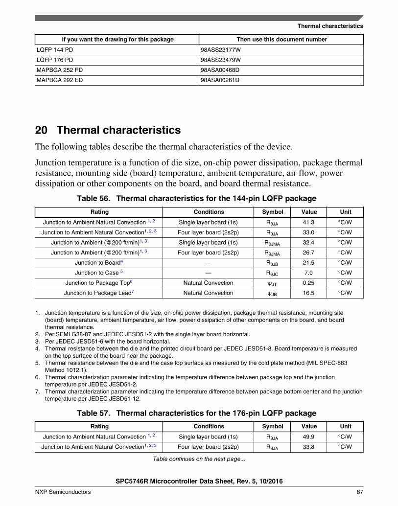
If you want the drawing for this package Then use this document number
LQFP 144 PD 98ASS23177W
LQFP 176 PD 98ASS23479W
MAPBGA 252 PD 98ASA00468D
MAPBGA 292 ED 98ASA00261D
20 Thermal characteristicsThe following tables describe the thermal characteristics of the device.
Junction temperature is a function of die size, on-chip power dissipation, package thermalresistance, mounting side (board) temperature, ambient temperature, air flow, powerdissipation or other components on the board, and board thermal resistance.
Table 56. Thermal characteristics for the 144-pin LQFP package
Rating Conditions Symbol Value Unit
Junction to Ambient Natural Convection 1, 2 Single layer board (1s) RθJA 41.3 °C/W
Junction to Ambient Natural Convection1, 2, 3 Four layer board (2s2p) RθJA 33.0 °C/W
Junction to Ambient (@200 ft/min)1, 3 Single layer board (1s) RθJMA 32.4 °C/W
Junction to Ambient (@200 ft/min)1, 3 Four layer board (2s2p) RθJMA 26.7 °C/W
Junction to Board4 — RθJB 21.5 °C/W
Junction to Case 5 — RθJC 7.0 °C/W
Junction to Package Top6 Natural Convection ψJT 0.25 °C/W
Junction to Package Lead7 Natural Convection ψJB 16.5 °C/W
1. Junction temperature is a function of die size, on-chip power dissipation, package thermal resistance, mounting site(board) temperature, ambient temperature, air flow, power dissipation of other components on the board, and boardthermal resistance.
2. Per SEMI G38-87 and JEDEC JESD51-2 with the single layer board horizontal.3. Per JEDEC JESD51-6 with the board horizontal.4. Thermal resistance between the die and the printed circuit board per JEDEC JESD51-8. Board temperature is measured
on the top surface of the board near the package.5. Thermal resistance between the die and the case top surface as measured by the cold plate method (MIL SPEC-883
Method 1012.1).6. Thermal characterization parameter indicating the temperature difference between package top and the junction
temperature per JEDEC JESD51-2.7. Thermal characterization parameter indicating the temperature difference between package bottom center and the junction
temperature per JEDEC JESD51-12.
Table 57. Thermal characteristics for the 176-pin LQFP package
Rating Conditions Symbol Value Unit
Junction to Ambient Natural Convection 1, 2 Single layer board (1s) RθJA 49.9 °C/W
Junction to Ambient Natural Convection1, 2, 3 Four layer board (2s2p) RθJA 33.8 °C/W
Table continues on the next page...
Thermal characteristics
SPC5746R Microcontroller Data Sheet, Rev. 5, 10/2016
NXP Semiconductors 87

Table 57. Thermal characteristics for the 176-pin LQFP package (continued)
Rating Conditions Symbol Value Unit
Junction to Ambient (@200 ft/min)1, 3 Single layer board (1s) RθJMA 37.8 °C/W
Junction to Ambient (@200 ft/min)1, 3 Four layer board (2s2p) RθJMA 28.2 °C/W
Junction to Board4 — RθJB 21.0 °C/W
Junction to Case5 — RθJC 7.8 °C/W
Junction to Package Top6 Natural Convection ψJT 0.3 °C/W
Junction to Package Lead7 Natural Convection ψJB 13.0 °C/W
1. Junction temperature is a function of die size, on-chip power dissipation, package thermal resistance, mounting site(board) temperature, ambient temperature, air flow, power dissipation of other components on the board, and boardthermal resistance.
2. Per SEMI G38-87 and JEDEC JESD51-2 with the single layer board horizontal.3. Per JEDEC JESD51-6 with the board horizontal.4. Thermal resistance between the die and the printed circuit board per JEDEC JESD51-8. Board temperature is measured
on the top surface of the board near the package.5. Thermal resistance between the die and the case top surface as measured by the cold plate method (MIL SPEC-883
Method 1012.1).6. Thermal characterization parameter indicating the temperature difference between package top and the junction
temperature per JEDEC JESD51-2.7. Thermal characterization parameter indicating the temperature difference between package bottom center and the junction
temperature per JEDEC JESD51-12.
Table 58. Thermal characteristics for the 252-pin MAPBGA package with full solder balls
Rating Conditions Symbol Value Unit
Junction to Ambient Natural Convection 1, 2 Single layer board (1s) RθJA 43.0 °C/W
Junction to Ambient Natural Convection1, 2, 3 Four layer board (2s2p) RθJA 26.5 °C/W
Junction to Ambient (@200 ft/min)1, 3 Single layer board (1s) RθJMA 33.2 °C/W
Junction to Ambient (@200 ft/min)1, 3 Four layer board (2s2p) RθJMA 22.2 °C/W
Junction to Board4 — RθJB 12.5 °C/W
Junction to Case5 — RθJC 6.3 °C/W
Junction to Package Top6 Natural Convection ψJT 0.3 °C/W
Junction to Package Lead7 Natural Convection ψJB 8.7 °C/W
1. Junction temperature is a function of die size, on-chip power dissipation, package thermal resistance, mounting site(board) temperature, ambient temperature, air flow, power dissipation of other components on the board, and boardthermal resistance.
2. Per SEMI G38-87 and JEDEC JESD51-2 with the single layer board horizontal.3. Per JEDEC JESD51-6 with the board horizontal.4. Thermal resistance between the die and the printed circuit board per JEDEC JESD51-8. Board temperature is measured
on the top surface of the board near the package.5. Thermal resistance between the die and the case top surface as measured by the cold plate method (MIL SPEC-883
Method 1012.1).6. Thermal characterization parameter indicating the temperature difference between package top and the junction
temperature per JEDEC JESD51-2.
Thermal characteristics
SPC5746R Microcontroller Data Sheet, Rev. 5, 10/2016
88 NXP Semiconductors

7. Thermal characterization parameter indicating the temperature difference between package bottom center and the junctiontemperature per JEDEC JESD51-12.
Table 59. Thermal characteristics for the 252-pin MAPBGA package 16 removed balls: 12central, 4 corner peripheral
Rating Conditions Symbol Value Unit
Junction to Ambient Natural Convection1, 2, 3 Four layer board (2s2p) RθJA 23.8 °C/W
Junction to Board4 Four layer board (2s2p) RθJB 15.9 °C/W
Junction to Package Lead5 Natural Convection ψJB 4.8 °C/W
1. Junction temperature is a function of die size, on-chip power dissipation, package thermal resistance, mounting site(board) temperature, ambient temperature, air flow, power dissipation of other components on the board, and boardthermal resistance.
2. Per SEMI G38-87 and JEDEC JESD51-2 with the single layer board horizontal.3. Per JEDEC JESD51-6 with the board horizontal.4. Thermal resistance between the die and the printed circuit board per JEDEC JESD51-8. Board temperature is measured
on the top surface of the board near the package.5. Thermal characterization parameter indicating the temperature difference between package bottom center and the junction
temperature per JEDEC JESD51-12.
20.1 General notes for specifications at maximum junctiontemperature
An estimation of the chip junction temperature, TJ, can be obtained from this equation:
TJ = TA + (RθJA × PD)
where:• TA = ambient temperature for the package (°C)• RθJA = junction to ambient thermal resistance (°C/W)• PD = power dissipation in the package (W)
The junction to ambient thermal resistance is an industry standard value that provides aquick and easy estimation of thermal performance. Unfortunately, there are two values incommon usage: the value determined on a single layer board and the value obtained on aboard with two planes. For packages such as the PBGA, these values can be different bya factor of two. Which value is closer to the application depends on the power dissipatedby other components on the board. The value obtained on a single layer board isappropriate for the tightly packed printed circuit board. The value obtained on the boardwith the internal planes is usually appropriate if the board has low power dissipation andthe components are well separated.
When a heat sink is used, the thermal resistance is expressed in the following equation asthe sum of a junction-to-case thermal resistance and a case-to-ambient thermal resistance:
RθJA = RθJC + RθCA
Thermal characteristics
SPC5746R Microcontroller Data Sheet, Rev. 5, 10/2016
NXP Semiconductors 89

where:• RθJA = junction to ambient thermal resistance (°C/W)• RθJC = junction to case thermal resistance (°C/W)• RθCA = case to ambient thermal resistance (°C/W)
RθJC is device related and cannot be influenced by the user. The user controls the thermalenvironment to change the case to ambient thermal resistance, RθCA. For instance, theuser can change the size of the heat sink, the air flow around the device, the interfacematerial, the mounting arrangement on printed circuit board, or change the thermaldissipation on the printed circuit board surrounding the device.
To determine the junction temperature of the device in the application when heat sinksare not used, the Thermal Characterization Parameter (ΨJT) can be used to determine thejunction temperature with a measurement of the temperature at the top center of thepackage case using this equation:
TJ = TT + (ΨJT × PD)
where:• TT = thermocouple temperature on top of the package (°C)• ΨJT = thermal characterization parameter (°C/W)• PD = power dissipation in the package (W)
The thermal characterization parameter is measured per JESD51-2 specification using a40 gauge type T thermocouple epoxied to the top center of the package case. Thethermocouple should be positioned so that the thermocouple junction rests on thepackage. A small amount of epoxy is placed over the thermocouple junction and overabout 1 mm of wire extending from the junction. The thermocouple wire is placed flatagainst the package case to avoid measurement errors caused by cooling effects of thethermocouple wire.
21 Ordering informationTable 60. Ordering information
Part Number Device Type Flash/SRAM Emulation RAM Package Frequency
SPC5746RK1MMT5 Sample PD1 4M / 256 KB - 252 MAPBGA 200 MHz
SPC5745RK1MLU3 Sample PD 3M / 192 KB - 176 LQFP 150 MHz
SPC5743RK1MLQ5 Sample PD 2M / 128 KB - 144 LQFP 200 MHz
PPC5746R2K1MMZ5A Sample ED2 4M / 256 KB 1 MB 292 MAPBGA 200 MHz
1. "PD" refers to a production device, orderable in quantity.2. “ED" refers to an emulation device, orderable in limited quantities. An emulation device (ED) is for use during system
development only and is not to be used in production. An ED is a Production PD chip combined with a companion chip toform an Emulation and Debug Device (ED) and includes additional RAM memory and debug features. EDs are provided
Ordering information
SPC5746R Microcontroller Data Sheet, Rev. 5, 10/2016
90 NXP Semiconductors

“as is" without warranty of any kind. In the event of a suspected ED failure, Freescale agrees to exchange the suspectedfailing ED from the customer at no additional charge, however Freescale will not analyze ED returns.
22 Revision historyTable 61. Revision history
Revision Date Description of changes
1 05/2013 Initial release.
2 12/2014 Overall:• Editorial changes.• Removed the Classification columns in spec tables and removed statements that values need
to be characterized.• In footnotes changed cross references to figures to static text.
In section Block diagram :• In Figure 1, changed "AIPS Bridge 0/1" to "AIPS PBridge_0/1".• In Figure 2 :
• Changed figure title (was “Peripherals block diagram”).• Changed "BAF" to "BAR".• Added PBRIDGE_1, EIM, XBAR, and PBRIDGE_0.
In section Introduction, removed section "Parameter classification".
In section Absolute maximum ratings, Table 1 :• VDD_HV_IO_FEC spec: removed row for "Using Ethernet Reference to VSS" condition.• Corrected "VIDD_HV_IO_MSC" to "VDD_HV_IO_MSC".• Add parameter IIOMAX.• Deleted IMAXSEG parameter.
In section Operating conditions :• Deleted sentence "The ranges in this table are design targets...".• Added a NOTE that all power supplies need to be powered up.• In Table 3 :
• Removed VDD_HV_FLA.• Changed minimum voltage of VDD_HV_ADV_SD.• Modified footnote for S/D ADC supply voltage.• Modified footnote for SAR ADC supply voltage.• Modified VRAMP spec to two separate specs for "VRAMP_VDD_LV" and
"VRAMP_VDD_HV_IO_MAIN, VRAMP_VDD_HV_PMC".
In section DC electrical specifications :• Removed the statement that the ranges are design targets.• In Table 5 :
• Modified IDD_LV to show specs depending on device model. Modified footnote.• Removed the “PMC only” row of the IDD_HV_PMC “internal core reg bypassed” spec.• Removed IDD_MAIN_CORE_AC.• Removed IDD_LKSTP_AC.• Changed IDDSTBY_ON value at 40 °C.• Changed IDDSTBY_REG parameter to "32 KB RAM Standby Regulator Current" (was
"Standby Leakage Current"); changed condition to "VDDSTBY @1.2 V to 5.9 V, Tj =150C" (was "VDDSTBY @1.3 V...")
• Removed IDDOFF.• Added IDD_BD_STBY.• Added IVDDA.
Table continues on the next page...
Revision history
SPC5746R Microcontroller Data Sheet, Rev. 5, 10/2016
NXP Semiconductors 91
Table 61. Revision history
Revision Date Description of changes
In section Input pad specifications :• In Table 7 :
• Added footnote that supported input levels vary according to pad types.• Corrected VILTTL Min and Max values.• Corrected VIHAUTO, VILCMOS_H and VILCMOS Min value.
• In Table 8 :• Modified |IWPU| Min values for condition Vin = VIH = 0.65 * VDD_HV_IO.• Modified |IWPD| Min values for condition Vin = VIL = 0.35 * VDD_HV_IO.
• Removed the "Analog Input Leakeage and Pull-Up/Down DC electrical characteristics" tableand the preceding introductory paragraph to be moved to the ADC input description section.
In section Output pad specifications, Table 9, changed VOH and VOL specs to two separate specsfor 3V pads and 5V pads respectively. Corrected VOH Min and VOL Max values.
In section I/O pad current specifications :• Added I/O Current Consumption tables.• Modified NOTE on Excel file attached to the Reference Manual.
Added section Reset pad (PORST, RESET) electrical characteristics.
In section Oscillator and FMPLL :• In Table 13, removed PLL0_PHI0 single period jitter row.• In Table 15 :
• Modified footnote for CS_EXTAL and CS_XTAL.• Modified gm (Oscillator Transconductance) spec.• Removed VHYS.
In section ADC modules, revised the subsection structure and titles:• Added section ADC input description with content moved from the "Input pad specifications"
section.• Section "Input impedance and ADC accuracy" renamed to Input equivalent circuit and ADC
conversion characteristics with all content except Figure 11 and Table 19 removed.• Removed erroneous section "SAR ADC electrical specification".
In section SAR ADC, Table 19 :• Added footnote ("SAR ADC performance is not guaranteed...") to fCK symbol.• Changed tsample specification min value to 250 ns (was 275).• Added footnote to OFS and GNE. Changed OFS and GNE min and max values.• Removed "Input (singe ADC channel)".• Removed injection row for "Input (double ADC channel)".• SNR, THD, SINAD, and ENOB specifications: changed frequency condition to 50 kHz (was
125 kHz).• Changed SNR Min values.• Added footnote to ENOB.• Added IDD_VDDA, IDD_VDDR, and VBG_REF parameters.
In section S/D ADC, Table 20 :• For VIN_PK2PK parameter second and third rows, changed VSS in Conditions to VDD.• For fADCD_M specification, removed sampling frequency footnote from parameter.• Added footnote to RESOLUTION value.• For |δGAIN| specification added footnote to parameter and added new row with more detailed
"After calibration" conditions.• Moved footnote "S/D ADC is functional in the range..." from the ZIN to the SNR parameters.• Changed all instances of “4.0 < VDD_HV_ADV_SD < 5.5” in the Conditions column to “4.5 <
VDD_HV_ADV_SD < 5.5”. Modified voltage range in its footnote.• Changed SNRSE150, GAIN = 16 condition min value to 55 dB (was 60).• Changed SINADSE150, GAIN = 16 condition min value to 54 dB (was 59).
Table continues on the next page...
Revision history
SPC5746R Microcontroller Data Sheet, Rev. 5, 10/2016
92 NXP Semiconductors

Table 61. Revision history
Revision Date Description of changes
• Unit for SINADDIFF150, SINADDIFF333 and SINADSE150 changed from dBFs to dB.• For ZIN specification, revised parameter footnote.• Added CMRR to symbol column for Common mode rejection ratio specification. Changed min
value to 55 dB.• For δGROUP specification, revised maximum values for OSR = 24 to OSR = 256 conditions.• Revised entire row for tLATENCY, tSETTLING, and tODRECOVERY specifications. Footnote added to
tLATENCY parameter.• Added IBIAS specification.• Changed IADV_D and ΣIADR_D values.
In section Temperature sensor, Table 21 :• Changed TACC values.• Removed ITEMP_SENS spec item.
In section LFAST interface timing diagrams, Figure 12, "|ΔVOD|" changed to "|VOD|".
In section LFAST and MSC /DSPI LVDS interface electrical characteristics, Table 24, the max.value for Rise/ Fall time specs changed from 4.0 to 5.7 ns.
In section LFAST PLL electrical characteristics, Table 25, ΔPEREYE specification, changed Nominalvalue to 550 (was blank) and Max value to blank (was 400).
In section Recommended power transistors, Table 27, added the specification for VC.
In section Power management integration :• In Figure 17 :
• Changed "n x CLV" to "CLV".• Changed CHV_ADC_S to CHV_ADC_SAR.
• In Table 28 :• Changed the first footnote for CHV_PMC to have the same footnote number as the first
footnote for CLV as they were identical.• Modified Minimum VDD_HV_ADV_SAR external capacitance and associated footnote.
Added section Regulator example for the NJD2873 transistor.
Added section Regulator example for the 2SCR574d transistor.
In section Device voltage monitoring, Table 29 :• Updated following specs:
• LVD_core_hot• LVD_core_cold• HVD_core• LVD_HV• HVD_HV• LVD_IO• LVD_SAR
• Removed following specs:• LVD_FLASH• HVD_FLASH• LVD_MSC_3V3• LVD_MSC_5V0• LVD_FEC_5V0• LVD_JTAG• HVD_SAR• LVD_SD• HVD_SD
• Corrected Voltage detector threshold crossing assertion Unit.
In section Flash memory program and erase specifications, Table 30 :
Table continues on the next page...
Revision history
SPC5746R Microcontroller Data Sheet, Rev. 5, 10/2016
NXP Semiconductors 93

Table 61. Revision history (continued)
Revision Date Description of changes
• Removed parenthetical phrase from table title.• Made overall updates to spec values.• Removed footnote 7.
In section Flash memory Array Integrity and Margin Read specifications, Table 31 :• Removed parenthetical phrase from table title.• Made overall updates to spec values.
In section Flash memory module life specifications, Table 32, removed parenthetical phrase fromtable title.
In section Flash memory AC timing specifications, Table 33, removed parenthetical phrase fromtable title.
Added section Flash read wait state and address pipeline control settings.
In section Power management integration, Table 28, changed the footnotes for tTCYC Min values tohave the same footnote number as they were identical.
In section DSPI timing with CMOS and LVDS, Table 39, LVDS (Master mode) specification:changed Max usuable frequency to 40 MHz (was 33 MHz).
In section DSPI CMOS master mode – classic timing :• Added NOTE.• In Table 40, changed PCS strobe timing values.
In section DSPI CMOS master mode – modified timing :• Added NOTE.• In Table 41, changed PCS strobe timing values.
In section DSPI LVDS master mode – modified timing, Table 42, changed significant digits for somevalues.
In section DSPI master mode – output only :• Modified format paragraphs leading the tables. Removed NOTE.• In Table 43, changed the tCSV strong drive value and tHO LVDS value.• In Table 44, changed significant digits for some values.
In section FEC timing, corrected the title of MII-lite and RMII serial management channel timingsubsections.
In section MII-lite transmit signal timing (TXD[3:0], TX_EN, TX_ER, TX_CLK), Table 47, modifiedfootnote for output parameters.
In section RMII serial management channel timing (MDIO and MDC), added Note on reference fortiming specifications.
In section RMII transmit signal timing (TXD[1:0], TX_EN), Table 52, modified R6 max value.
In section UART timings, Table 53, removed 100 MHz specification.
"Package drawings" section renamed to Obtaining package dimensions, with package drawingdocument numbers to search at the Freescale website. Drawings removed from this document.
In section Thermal characteristics :• Added table for 144 LQFP.• Moved table for 176 LQFP before 252 MAPBGA and updated table.• Replaced table for 252 MAPBGA with two separate tables for package with full solder balls
and package with 16 removed balls.
In section Ordering information, replaced the table.
3 09/2015 On the cover page:
Table continues on the next page...
Revision history
SPC5746R Microcontroller Data Sheet, Rev. 5, 10/2016
94 NXP Semiconductors

Table 61. Revision history
Revision Date Description of changes
• Changed doctype from "Data Sheet: Product Preview" to "Data Sheet: Technical Data" at theupper left corner.
• Changed statement on status of doc at the bottom of the page.
Removed "Preliminary" and "Non-Disclosure Agreement required" from footers on each page.
In section Electromagnetic Compatibility (EMC) removed content of entire section and replaced itwith statement: "EMC measurements to IC-level IEC standards are available from Freescale onrequest."
In section Operating conditions :• In Table 3
• For VDD_HV_PMC, removed the two footnotes.• For VDDSTBY, added statement on ramp rate to footnote.• For VSTBY_BO, removed Min value and added Max value.
In section DC electrical specifications :• In Table 5 :
• IDD_LV spec:• MPC5746R/MPC5745R Max value changed to 700 mA.• MPC5743R/MPC5742R Max value changed to 610 mA.
• IDDSTBY_ON TA=40°C and TA=85°C values updated.• IVDDA values updated.
In section I/O pad specification, Table 6 Description for Input only pads, removed reference to"Automotive" input.
In section Input pad specifications, Table 7 removed VIHAUTO, VILAUTO, VHYSAUTO, andVDRFTAUTO specs and references to "Automotive" input in footnotes.
In section Output pad specifications :• In Table 9, removed footnote for tR_F spec Parameter about transition time maximum value
approximation formula.
In section Reset pad (PORST, RESET) electrical characteristics :• In Table 12 :
• Changed specs for VIH, VIL, and VHYS to VIH Reset, VIL Reset, and VHYS Resetrespectively.
• Added specs for VIH PORST, VIL PORST, VHYS PORST.• Generally added Conditions and updated spec values. In the Conditions column,
changed all instances of "3.0 V" to "3.5 V".
In section Oscillator and FMPLL :• In Table 13, for ΔPLL0LTJ spec, modified long term jitter Min and Max values.• In Table 16, values updated.• In Table 17, added spec for dfTRIM (IRC software trimming step).
In section ADC input description :• In Table 18 :
• RPUPD 5KΩ spec Max value changed to 8.8KΩ.
In section Input equivalent circuit and ADC conversion characteristics :• In Table 19 :
• In the SNR, THD, SINAD, and ENOB rows Conditions, changed "50 kHz" to "125 kHz".Modified footnote to ENOB
• In IDD_VDDA and IDD_VDDR rows, modified values.• In VBG_REF row's Conditions, added "INPSAMP=0xFF"
Table continues on the next page...
Revision history
SPC5746R Microcontroller Data Sheet, Rev. 5, 10/2016
NXP Semiconductors 95

Table 61. Revision history (continued)
Revision Date Description of changes
• Added NOTE "For spec complaint operation, do not expose clock sources, including crystaloscillator, IRC, PLL0, and PLL1 on the CLKOUT pads while the SAR ADC is converting."
• Added NOTE: "The ADC performance specifications are not guaranteed if two or more ADCssimultaneously sample the same shared channel".
In section S/D ADC :• In Table 20 :
• For THDDIFF333 GAIN = 16, updated Min value.• For IADV_D, updated Max value.
In section LFAST and MSC /DSPI LVDS interface electrical characteristics :• After table Table 24 added NOTE "For optimum LVDS performance, it is recommended to set
the neighbouring GPIO pads to use Weak Drive".
In section Device voltage monitoring :• In Table 29 :
• For LVD_core_hot, LVD_HV, and LVD_IO specs, removed the untrimmed Risingvoltage and Falling voltage rows.
• For LVD_core_hot, changed Mask Opt. value to "No".
In section Regulator example for the 2SCR574d transistor, figure "Regulator example", changed “5Vor Vcollector” to “3.3V or Vcollector”.
In section DSPI CMOS master mode – classic timing, Table 40 :• Changed tSDC spec's Condition SCK drive strength from "0 pF" to "0 to 50 pF".• In tSUI and tHI specs' footnote, removed reference to "Automotive" thresholds.
In section DSPI CMOS master mode – modified timing, Table 41 :• Changed tSDC spec's Condition SCK drive strength from "0 pF" to "0 to 50 pF".• In tSUI and tHI specs' footnote, removed reference to "Automotive" thresholds.
In section DSPI master mode – output only, Table 44, changed tSDC spec's Condition SCK drivestrength from "0 pF" to "0 to 50 pF".
Added section eMIOS timing.
In section Ordering information, Table 60 :• Updated Part Numbers.• Updated Emulation device footnote.
4 03/2016 In section Block diagram, Figure 2 :• "DECIM" changed to "DECFILTER".• "SIPI" changed to "Zipwire".• I/O lines added to Zipwire, SIUL2, REACM, eTPU, eMIOS, IGF, and XOSC.
In section Absolute maximum ratings table "Absolute maximum ratings", removed IIOMAX spec andadded IMAXSEG spec.
In section Operating conditions table "Device operating conditions":• For the FEC I/O supply voltage, MSC I/O supply voltage, and JTAG I/O supply voltage specs,
removed the LVD enabled/disabled distinction.• Added footnote to IMAXSEG.
In section I/O pad current specifications :• Modified the descriptions in the two paragraphs after the tables.• Removed the third paragraph after the tables and the first Note.
Added section DSPI CMOS slave mode.
Table continues on the next page...
Revision history
SPC5746R Microcontroller Data Sheet, Rev. 5, 10/2016
96 NXP Semiconductors

Table 61. Revision history (continued)
Revision Date Description of changes
In section Ordering information table "Ordering Information", changed Part Numbers for the 176LQFP PD and the ED.
5 10/2016 Editorial updates.
In section Operating conditions table "Device operating conditions" added foootnote toVDD_HV_IO_JTAG.
In section Input pad specifications table "I/O input DC electrical characteristics" for ILKG addedcondition "VSS < VIN < VDD_HV_IO*"
In section ADC input description table "Analog Input Leakage and Pull-Up/Down DC electricalcharacteristics" for ILK_AD added conditions "VSS_HV_ADV_SAR < VIN < VDD_HV_ADV_SAR" and"VSS_HV_ADV_SD < VIN < VDD_HV_ADV_SD".
In section Recommended power transistors table "Recommended operating characteristics" forICMaxDC changed the parameter from "Minimum peak collector current" to "Maximum DC collectorcurrent".
In section SAR ADC table "ADC conversion characteristics":• Removed the condition for tsample.• Removed the Min and added the formula (6.02*ENOB) + 1.76 for SINAD.• Changed the Min value from 650 to 700 for tconv.
In section S/D ADC table "SDn ADC electrical specification":• Removed ZIN specification• Added ZDIFF, ZCM, and ΔVINTCM specifications• For RBIAS:
• Changed Parameter description from "Bias resistance" to "Bare bias resistance"• Changed Min from 100 kΩ to 110 kΩ• Changed Typ from 125 kΩ to 144 kΩ• Changed Max from 160 kΩ to 180 kΩ
In section Flash memory AC timing specifications table "Flash memory AC timing specifications" fortpsus:
• Changed Typical from 7 μs plus four system clock periods to 9.4 μs plus four system clockperiods
• Changed Max from 9.1 μs plus four system clock periods to 11.5 μs plus four system clockperiods
Revision history
SPC5746R Microcontroller Data Sheet, Rev. 5, 10/2016
NXP Semiconductors 97

How to Reach Us:
Home Page:nxp.com
Web Support:nxp.com/support
Information in this document is provided solely to enable system and software
implementers to use NXP products. There are no express or implied copyright
licenses granted hereunder to design or fabricate any integrated circuits based
on the information in this document. NXP reserves the right to make changes
without further notice to any products herein.
NXP makes no warranty, representation, or guarantee regarding the suitability of
its products for any particular purpose, nor does NXP assume any liability arising
out of the application or use of any product or circuit, and specifically disclaims
any and all liability, including without limitation consequential or incidental
damages. “Typical” parameters that may be provided in NXP data sheets and/or
specifications can and do vary in different applications, and actual performance
may vary over time. All operating parameters, including “typicals,” must be
validated for each customer application by customerʼs technical experts. NXP
does not convey any license under its patent rights nor the rights of others. NXP
sells products pursuant to standard terms and conditions of sale, which can be
found at the following address: nxp.com/SalesTermsandConditions.
NXP, the NXP logo, NXP SECURE CONNECTIONS FOR A SMARTER
WORLD, COOLFLUX, EMBRACE, GREENCHIP, HITAG, I2C BUS, ICODE,
JCOP, LIFE VIBES, MIFARE, MIFARE CLASSIC, MIFARE DESFire, MIFARE
PLUS, MIFARE FLEX, MANTIS, MIFARE ULTRALIGHT, MIFARE4MOBILE,
MIGLO, NTAG, ROADLINK, SMARTLX, SMARTMX, STARPLUG, TOPFET,
TRENCHMOS, UCODE, Freescale, the Freescale logo, AltiVec, C-5, CodeTest,
CodeWarrior, ColdFire, ColdFire+, C-Ware, the Energy Efficient Solutions logo,
Kinetis, Layerscape, MagniV, mobileGT, PEG, PowerQUICC, Processor Expert,
QorIQ, QorIQ Qonverge, Ready Play, SafeAssure, the SafeAssure logo,
StarCore, Symphony, VortiQa, Vybrid, Airfast, BeeKit, BeeStack, CoreNet,
Flexis, MXC, Platform in a Package, QUICC Engine, SMARTMOS, Tower,
TurboLink, and UMEMS are trademarks of NXP B.V. All other product or service
names are the property of their respective owners. ARM, AMBA, ARM Powered,
Artisan, Cortex, Jazelle, Keil, SecurCore, Thumb, TrustZone, and μVision are
registered trademarks of ARM Limited (or its subsidiaries) in the EU and/or
elsewhere. ARM7, ARM9, ARM11, big.LITTLE, CoreLink, CoreSight,
DesignStart, Mali, mbed, NEON, POP, Sensinode, Socrates, ULINK and
Versatile are trademarks of ARM Limited (or its subsidiaries) in the EU and/or
elsewhere. All rights reserved. Oracle and Java are registered trademarks of
Oracle and/or its affiliates. The Power Architecture and Power.org word marks
and the Power and Power.org logos and related marks are trademarks and
service marks licensed by Power.org.
© 2013–2016 NXP B.V.
Document Number MPC5746RRevision 5, 10/2016