Embed Size (px)
Citation preview

A thesis submitted in partial satisfaction of the
requirements for the degree of
Master of Computer Science and Engineering
in the Graduate School of
the University of Aizu
OASIS Network-on-Chip
Prototyping on FPGA
by
m5141120
Kenichi Mori
February 2012

The thesis titled
OASIS Network-on-ChipPrototyping on FPGA
by
m5141120Kenichi Mori
is reviewed and approved by:
Main referee
Associate Professor Date
Ben Abdallah Abderazek
Professor Date
Kenichi Kuroda
Assistant Professor Date
Hiroshi Saito
The University of Aizu
February 2012

Contents
Chapter 1 Introduction 11.1 Background . . . . . . . . . . . . . . . . . . . . . . . . . . . . . . . 11.2 Problems and Contributions . . . . . . . . . . . . . . . . . . . . . . 21.3 Related Works . . . . . . . . . . . . . . . . . . . . . . . . . . . . . . 4
1.3.1 Comparison between NoC and Bus . . . . . . . . . . . . . . 41.3.2 FPGA Prototyping . . . . . . . . . . . . . . . . . . . . . . . 41.3.3 Topology Optimizations . . . . . . . . . . . . . . . . . . . . 4
1.4 Thesis Organization . . . . . . . . . . . . . . . . . . . . . . . . . . . 5
Chapter 2 OASIS Network-on-Chip Overview 62.1 On Chip Interconnection . . . . . . . . . . . . . . . . . . . . . . . . 6
2.1.1 Topology and Routing . . . . . . . . . . . . . . . . . . . . . 62.1.2 Switching . . . . . . . . . . . . . . . . . . . . . . . . . . . . 72.1.3 Flow Control . . . . . . . . . . . . . . . . . . . . . . . . . . 72.1.4 Arbiter . . . . . . . . . . . . . . . . . . . . . . . . . . . . . 72.1.5 Network Interface . . . . . . . . . . . . . . . . . . . . . . . 7
2.2 OASIS NoC Features . . . . . . . . . . . . . . . . . . . . . . . . . . 82.3 OASIS Router Functions . . . . . . . . . . . . . . . . . . . . . . . . 8
Chapter 3 System Architecture 103.1 Switching Mechanism . . . . . . . . . . . . . . . . . . . . . . . . . 103.2 Buffer Design . . . . . . . . . . . . . . . . . . . . . . . . . . . . . . 113.3 Avoiding Buffer Overflow . . . . . . . . . . . . . . . . . . . . . . . 123.4 OASIS Arbiter Design . . . . . . . . . . . . . . . . . . . . . . . . . 143.5 Abstraction of Target Application . . . . . . . . . . . . . . . . . . . 173.6 Network Interface (NI) Design . . . . . . . . . . . . . . . . . . . . . 183.7 Short Pass Link (SPL) Approach . . . . . . . . . . . . . . . . . . . . 21
3.7.1 SPL Insertion Algorithm . . . . . . . . . . . . . . . . . . . . 213.7.2 Additional Ports Area Utilization . . . . . . . . . . . . . . . 233.7.3 Modifications for SPL . . . . . . . . . . . . . . . . . . . . . 23
Chapter 4 Evaluation Results 274.1 Environments and Parameters . . . . . . . . . . . . . . . . . . . . . . 274.2 Dimension Reversal and Hotspot Simulation Results . . . . . . . . . 274.3 JPEG Encoder Simulation Results . . . . . . . . . . . . . . . . . . . 294.4 Hardware Design Analysis . . . . . . . . . . . . . . . . . . . . . . . 31
iii

4.5 Power Consumption Analysis . . . . . . . . . . . . . . . . . . . . . . 31
Chapter 5 Conclusion 34
Publication 38
iv
List of Figures
Figure 1.1 Typical paradigms (a) circuit switching, (b) packet switchingmodel . . . . . . . . . . . . . . . . . . . . . . . . . . . . . . . . . . 2
Figure 1.2 Typical standard topology, (a) N x M mesh topology, (b) 3 stageClos topology . . . . . . . . . . . . . . . . . . . . . . . . . . . . . . 2
Figure 1.3 Typical customized topology . . . . . . . . . . . . . . . . . . 3
Figure 2.1 3 x 3-mesh topology . . . . . . . . . . . . . . . . . . . . . . . 6Figure 2.2 NoC with Network Interface . . . . . . . . . . . . . . . . . . 7
Figure 3.1 A router block diagram . . . . . . . . . . . . . . . . . . . . . 10Figure 3.2 OASIS and OASIS-2 transmission time at different buffer size . 11Figure 3.3 4x4 mesh topology . . . . . . . . . . . . . . . . . . . . . . . 12Figure 3.4 RTL view of Input module . . . . . . . . . . . . . . . . . . . 13Figure 3.5 RTL view of mesh-topology with SPL . . . . . . . . . . . . . 13Figure 3.6 (a) state machine design for stall go, (b) statement of nearly full
signal output . . . . . . . . . . . . . . . . . . . . . . . . . . . . . . . 14Figure 3.7 Stall go block diagram . . . . . . . . . . . . . . . . . . . . . . 14Figure 3.8 Matrix arbitration example . . . . . . . . . . . . . . . . . . . 15Figure 3.9 Arbiter control signals . . . . . . . . . . . . . . . . . . . . . . 15Figure 3.10 RTL view of switch allocator . . . . . . . . . . . . . . . . . . 16Figure 3.11 RTL view of crossbar . . . . . . . . . . . . . . . . . . . . . . 17Figure 3.12 Dimension reversal . . . . . . . . . . . . . . . . . . . . . . . 17Figure 3.13 Hotspot . . . . . . . . . . . . . . . . . . . . . . . . . . . . . 17Figure 3.14 JPEG encoder block diagram . . . . . . . . . . . . . . . . . . 18Figure 3.15 Task Mapping . . . . . . . . . . . . . . . . . . . . . . . . . . 18Figure 3.16 A sample transmitter NI block diagram . . . . . . . . . . . . . 19Figure 3.17 A sample receiver NI block diagram . . . . . . . . . . . . . . 19Figure 3.18 JPEG encoder packet transmission patterns . . . . . . . . . . . 20Figure 3.19 Flits’ structure . . . . . . . . . . . . . . . . . . . . . . . . . . 21Figure 3.20 Sample of Shot Pass Link . . . . . . . . . . . . . . . . . . . . 21Figure 3.21 SPL insertion algorithm . . . . . . . . . . . . . . . . . . . . . 22Figure 3.22 Extra-Port insertion . . . . . . . . . . . . . . . . . . . . . . . 24Figure 3.23 Dimension reversal with 2 SPLs . . . . . . . . . . . . . . . . 24Figure 3.24 Hotspot with 2 SPLs . . . . . . . . . . . . . . . . . . . . . . . 24Figure 3.25 JPEG encoder with 3 SPLs . . . . . . . . . . . . . . . . . . . 25Figure 3.26 RTL view of NoC with JPEG encoder . . . . . . . . . . . . . 26
Figure 4.1 Dimension reversal simulation result . . . . . . . . . . . . . . 29
v
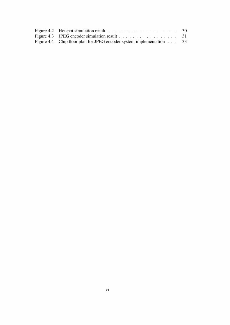
Figure 4.2 Hotspot simulation result . . . . . . . . . . . . . . . . . . . . 30Figure 4.3 JPEG encoder simulation result . . . . . . . . . . . . . . . . . 31Figure 4.4 Chip floor plan for JPEG encoder system implementation . . . 33
vi

List of Tables
Table 3.1 OASIS and ONoC hardware performance. BD:buffer depth . . . 11Table 3.2 5-ports OASIS Router Area Utilization . . . . . . . . . . . . . 23Table 3.3 6-ports OASIS Router Area Utilization . . . . . . . . . . . . . 23
Table 4.1 Dimension reversal simulation environment . . . . . . . . . . . 28Table 4.2 Hotspot simulation environment . . . . . . . . . . . . . . . . . 28Table 4.3 JPEG encoder simulation environment . . . . . . . . . . . . . . 28Table 4.4 Hardware complexity: Dimension reversal . . . . . . . . . . . 29Table 4.5 Hardware complexity: Hotspot . . . . . . . . . . . . . . . . . . 30Table 4.6 Hardware complexity: JPEG encoder . . . . . . . . . . . . . . 30
vii

Acknowledgement
I wish to express my appreciation to Prof. Ben A. Abderazek for his excellent adviceand diligent efforts to guide me through this project. And he gave me good oppor-tunities to improve my skills, including that are a way of studying English. Also Iwould like to appreciate to Prof. Hiroshi Saito and Prof. Kenichi Kuroda of Univer-sity of Aizu for revising my thesis. Moreover Prof. Yuichi Okuyama and Prof. JunjiKitamichi who helped with my troubles and problems during my project.
Finally, I am deeply grateful to the members of the Adaptive Systems Laboratoryat the University of Aizu. These people have supported not only researches but alsomy school life. I could not have marvelous days in the University of Aizu without a lotof great friends.
viii

Abstract
Network-on-Chip (NoC) architectures provide a good way of realizing efficientinterconnections and largely alleviate the limitations of bus-based solutions.
NoC has emerged as a solution to problems exhibited by the shared bus commu-nication approach in System-On-Chip (SoC) implementations. This includes the lackof scalability, clock skew, lack of support for concurrent communication, and powerconsumption.
Network-on-Chip communication is realized by packet, the communication re-quirement of this paradigm is affected by architecture parameters selection such astopology, mapping, routing, buffer size etc... Focusing on topology, there are 2 se-lections: regular topology and custom topology. These choices also affect hardwarecomplexity and performance.
The challenges in this thesis are the designing of a prototype NoC with a real ap-plication including parallel execution and inserting Short Pass Link (SPL) to regular2D-mesh topology NoC as an optimization technique and prototyping on FPGA toevaluate its performance and hardware complexity accurately. The optimization is ex-ecuted based on our designed NoC named OASIS, JPEG encoder, which is selectedas a target real application, is divided into 8 tasks to be mapped to each node. Then,design appropriate Network Interface (NI) for the application tasks, and improve thecommunication delay by employing the SPL insertion algorithm. Finally, I evaluatedits communication performance improvement and accurate hardware utilization vari-ance.
I prototyped the system in hardware and I evaluated its performance in terms of la-tency and power using Dimension reversal transaction, Hotspot transaction, and a par-allelized JPEG encoder. From the performance evaluation results, I concluded that theDimension reversal execution time in ONoC with SPL decreased by 29.7%, when com-pared to the original base architecture, Hotspot execution time decreased by 16.9%,and JPEG encoder decreased by 43.7%. The area of these three test benches in ONoCwith SPL increased under 5%, the Dimension reversal increased by 2.93%, the Hotspotincreased by 2.60%, and the JPEG encoder increased by 4.28%. The power consump-tion slightly increased by 0.49% on average. The results indicate that the architectureis effective in balancing the power and performance of NoC design.


Chapter 1
Introduction
1.1 Background
Current Systems-on-Chip (SoC) executes applications that demand extensive amountsof parallel processing. Network-On-Chip (NoC) [1], [2], [3] provides a good way ofrealizing interconnections on silicon and largely alleviates the limitations of bus-basedsolutions. Deep sub-micron processing technologies have enabled the implementa-tion of new application-specific embedded architectures that integrate multiple soft-ware programmable processors and dedicated hardware components together onto asingle chip. Recently, this kind of architecture has emerged as key design solutionsfor today’s non-electronic design problems, which are being driven by emerging ap-plications in the areas of (1) wireless communication, (2) broadband/distributed net-working, (3) distributed computing, and (4) multimedia computing. NoC is becomingan attractive option for solving bus-based systems problems. It is a scalable architec-tural platform with a huge potential to handle the increasing complexity and which caneasily provide reconfigurability. In NoC architectures, processors are connected via apacket-switched communication network on a single chip. It is similar to the way thatcomputers are connected to Internet. The packet-switched network routes informationbetween network clients (e.g. processors, memories, and custom logic devices). Figure1.1 illustrates a typical NoC paradigm and point-to-point network. Packet switchingsupports asynchronous data transfer. It also provides extremely high bandwidth bydistributing the propagation delay across multiple switches, effectively pipelining thepacket transmission. In addition, NoC offers several promising features: First, it trans-mits packets instead of words. For that reason, dedicated address lines, like those inbus based systems, are not necessary since the destination addresses of packets are in-cluded in the packet. Second, transmission can be conducted in parallel if the networkprovides more than one transmission channel between a sender and a receiver. Thus,unlike bus-based Systems-on-Chip, NoC presents theoretical infinite scalability, facileIP core reusing, and higher level of parallelism.
1

Figure 1.1: Typical paradigms (a) circuit switching, (b) packet switching model
Figure 1.2: Typical standard topology, (a) N x M mesh topology, (b) 3 stage Clostopology
1.2 Problems and ContributionsWe previously designed a NoC named OASIS which is an n × n mesh-topology.
The NoC uses wormhole like switching, a First-Come-First-Served (FCFS) scheduler,and re-transmission flow control which is like ACK/NACK flow control. However theflow control, only source and destination core manage their flow control. OASIS NoCis a regular NoC architecture based on a grid-topology [1].
In our previous work, we optimized OASIS and we called it OASIS-2. As an opti-mization, OASIS-2 employs an avoiding buffer overflow technique instead of OASISre-transmission flow control (RFC) as flow control. The used avoiding buffer overflowtechnique efficiently prevents buffers from overflowing. Random Number Generator(RNG) transmission is used for simulation, and it achieves total transmission time isdecreased by 19.5% with 4.38% extra area utilization in average.
OASIS-2 still has optimized spaces for target applications. I proposed OptimizedOASIS NoC system(ONoC) which is a highly optimized for topology based on OASIS-2. OASIS-2 employed an n × m mesh topology which is a simple layout perspec-tive and the local interconnections between resources and switches are independent ofthe size of the network [4]. NoC topology has 2 choices; one is a standard such as
2
Grid-Topology (Mesh), torus, star, and clos. Figure 1.2 illustrates standard topologies.These architectures are not concerned for dedicated applications. Each processing el-ement (PE) is connected uniformly without consideration of the network load balanceand spots where increasing traffic is concentrated which may cause the packet dropsor stall transactions, and then degrades the overall performance significantly. Someresearchers attempted to solve these problems by increasing buffer size and the wires’width at the expense of the area utilization and power consumption. The other topol-ogy choice is custom topology, whose router cannot re-use, and the routing algorithmis difficult to implement. The routers have identical components (numbers of port,physical wires), so the design time is longer than standard. Figure 1.3 illustrates a typ-ical design of a custom topology. The significant increased design complexity of theNoC-based system causes unacceptable simulation time with the traditional simula-tion methods [5], [6]. The NoC architecture researches include a lot of trade-offs suchas: topology, routing, switching, scheduling, flow control, buffer size, packet size, andany optimization techniques. It is difficult to analyze in only high-level simulations.Therefore NoC prototype is an essential research for evaluating the performance of theNoC architecture under real applications [7].This thesis explores the algorithm to structure a partial custom topology, which is basedon a standard 2D mesh topology and inserts short pass link (SPL) for long range com-munications and the high frequency communication in whole data communication.These two elements can cause performance decline significantly. Then, I prototypedNoC and measured the performance of some traffics and real application and hardwarecomplexity.
Figure 1.3: Typical customized topology
3

1.3 Related Works
1.3.1 Comparison between NoC and BusNoC is becoming an attractive option for solving bus-based systems problems.
Evaluation comparisons are presented between NoC and shared-bus AMBA [8]. TheAMBA protocol is an open standard, on-chip bus specification. A single-layer centralmultiplexer configuration with pipelined transaction is used in this work. The NoC em-ploys mesh-based topology with deterministic XY routing with shortest path mappingbetween communicating cores. Single-flit-packet wormhole routing, and handshakeflow control. For comparison, MPEG-2 video decoder traffic in cycle-accurate real-istic simulation environment is used as real application. Supported by analytical andsimulation results, it has been shown that the NoC reduces decoding time by a factorof 2.46 on average compared to AMBA [9]. Some researchers compare and contrastthe Network-on-Chip (NoC) with Point-to-Point (P2P) and bus-based communicationarchitectures. The performance of the NoC-based implementation is very close to thatof the P2P for the same application. Moreover, the scalability analysis based on du-plicating the bottleneck module in the MPEG-2 design shows that the performance ofthe NoC design scales as well as the P2P, while the bus-based implementation scalesmuch more poorly [10].
1.3.2 FPGA PrototypingThe practical NoC interconnections’ fast and accurate performance evaluation and
design survey are the critical issue. Some researchers present a flexible HW/SW emu-lation environment implemented on an FPGA that is suitable to explore, evaluate, andcompare customized NoC [5]. However, they used Traffic Generator (TG), and did notuse a real application. An implementation on FPGA and explained how to implementNoC with multi cores in details are explained [6], but its execution time measurementwas in terms of assembly language instructions executed. These two papers mentionedhow to deeply implement on FPGA and no parameter trade-offs.
1.3.3 Topology OptimizationsThe IPs are mapped onto a standard topology or customized for a given applica-
tion. Standard topology can reduce the design time but it probably includes idlingports, whole customized topology needs additional design time but it can enhance theperformance. There is a design time and the performance trade-off. An approach thatautomatically selects the best topology for a given application and produces a mappingof cores onto that topology tool, named SUNMAP. The evaluation is executed withTG, and xpipes compiler [11] is used for hardware is presented in [12]. Fully cus-tomized topologies are shown in [13], which exploits the detailed understanding of thecommunication workload for optimization purpose, and they implemented proposedalgorithms in a C++ package. These topology optimizations are mostly evaluated insoftware level.In this thesis, the implementation on FPGA, and simulation under JPEG encoder as a
4

real application is done. Moreover, the hardware complexity and execution time eval-uation show the comparison with NoC architecture optimizations by inserting ShortPass Link (SPL).
1.4 Thesis OrganizationThis thesis presents the background, motivation, and some related works are intro-
duced in chapter 1. Chapter 2 explains OASIS Network-on-Chip overview which isour previously designed NoC. Chapter 3 explains system architecture of the design indetail and Short Pass Link insertion algorithm as an optimization technique, which canreduce the execution time unless large increasing area. Chapter 4 explains evaluationresults. Target device is Altera StratixIII and measurements of the execution time andhardware complexity results in details are shown. Last chapter concludes this thesis.
5

Chapter 2
OASIS Network-on-Chip Overview
2.1 On Chip Interconnection
The NoC interconnection paradigm is characterized by its topology, routing, switch-ing, flow control, and arbiter. There are various trade-offs between hardware-cost andperformance, and design-time and performance. So designers need to take care anddeeply understand about all design choices.
2.1.1 Topology and Routing
As I explained in Chap.1, Topology is commonly chosen from two types, stan-dard and customized. The routing methods are selected depending on the topology[14], [15]: standard topology (e.g. Mesh, Torus, Star, and etc.) can easily implementrouting mechanism because each router sends the same calculation or comparison, butcustomized topology is necessary to design specific routing mechanism, so the designtime may be longer than standard [16], [17]. Figure 2.1 illustrates 3 x 3 Network sizemesh topology.
Figure 2.1: 3 x 3-mesh topology
6

2.1.2 Switching
In packet switching, how the packets are passed between the routing nodes isknown as switching. The switching strategy influences the buffering in the routingnodes and how resources are used [18]. In the switching strategies, Store and Forward-ing (SF), Wormhole Switching (WS), and Virtual Cut Through (VCT) can be chosen.These switching methods transmit flits (flow control units), which are parts of individ-ual packets.
2.1.3 Flow Control
Flits must be transmitted in a way that there are no dropped flits, or with some kindof resend protocol. Low power consumption, and calculation time, are not dependenton situation of the network and are ideal for flow control. ON/OFF, Credit-based,Handshaking, and ACK/NACK are the commonly used control flows used in NoC[19].
2.1.4 Arbiter
Mesh topology, inputs and outputs of routers mostly have five directions: north,east, south, west, and local. It is acceptable for routers to have multiple inputs, butonly one input stream is processed and routed. To solve this competition when onlyone input can access to the same output, designer can use virtual channel switch, whereeach port of the switch has multiple parallel buffers [20]. But, this causes a significantlyhardware area utilization rise. Another solution is arbiter [21], it grants inputs whichtransmit for the same output stream.
2.1.5 Network Interface
The network interface (NI) has two functions, one is in the transmitter side, whichdivides a message data into payloads, generates flits and then transmits flits to the net-work. The other one is the receiver side, which assembles the incoming flits to generatethe data message that will be delivered to the attached PE. Figure 2.2 illustrates briefsample NI implementation in NoC.
Figure 2.2: NoC with Network Interface
7

2.2 OASIS NoC FeaturesWe previously designed a basic Network-on-Chip named OASIS [22]. The system
is a n × m mesh-topology and uses wormhole switching, a First-Come-First-Served(FCFS) scheduler, and a novel re-transmission flow control (RFC). The FCFS schedul-ing is a simple algorithm and was carefully designed to be suitable for implementationin hardware. The RFC scheme is implemented in the processing elements (PEs) them-selves; source nodes send checksum and the PEs of destination nodes confirm thecorrectness. If flits have been corrupted or dropped, they must be retransmitted. Inthis situation, new flits are resent from source PEs. Using this technique, OASIS cancorrectly transmit data even in noisy environments. The major drawback of OASIS isin its FCFS scheduler algorithm. The FCFS has unbalanced network utilization whenlooking at overall performance, because some transactions are served by the schedulerand other transactions are always stalled. This approach causes unbalanced networkutilization and increases the latency because the retransmission technique must re-send flits if errors occur. In our previous work, we optimized OASIS and we calledit OASIS-2. The system employs stall-go for avoiding buffer overflow, and matrix ar-biter for scheduler. It also supports wormhole-like switching and virtual-cut-throughforwarding method. The switching method which is chosen in a given instance de-pends on the level of packet fragmentation. Each router has input buffers which canstore up to four flits. When a packet is divided into more than four flits, OASIS-2chooses wormhole switching. When packets are divided into less than four flits, thesystem chooses virtual cut through. In other words, when buffer the size is greater thanor equal to the number of flits, virtual cut through is used, but when buffer size is lessthan or equal to the number of flits, wormhole switching is employed.
2.3 OASIS Router FunctionsOur early designed OASIS router provides extremely high bandwidth by distribut-
ing the propagation delay across multiple switches, thus pipelining the packet trans-mission. Our three-stage pipelined router architecture uses a speculative strategy basedon a simple look-ahead routing, where each flit additionally carries one hot encodednext-port identifier used by the downstream routers, in providing routing adaptation.Each router compares the current address and destination address to select the out-put port direction. OASIS router main functions are divided into routing calculation,arbitration & f low control, and data transmission. The first stage where; input flitsare stored in the input buffer. When the buffers are almost full it, sends a signal toupstream neighbor router. On the second stage, routing calculation is done by usingthe stored flits’ information. The flits’ stored module sends Request signal to the arbi-tration module, and then the arbiter selects the winner to access the output, and sendsGrant signal to the stored input module, this system based on least recently servedscheme. The flow control is employed to avoid dropping flits, and it uses a state ma-chine to manage the signals coming from downstream neighbor router about its inputmodule status and also the state router’s output data. Finally, the third stage whichtransmits flits that have included updated routing information and fixed payload to theadequate output direction. The router supports pipelined routing, so all calculations
8

and comparisons can execute in parallel.
9

Chapter 3
System Architecture
Figure 3.1: A router block diagram
Our designed router is three-stage pipelined router architecture. In this chapter, Iwould like to explain the three stages: first stage includes ”Buffer design”. Secondstage includes ”Routing”, ”Avoiding buffer overflow” and ”Scheduling”, and the thirdstage includes ”Crossbar”. Figure 3.1 illustrates the router block diagram, left fivemodules are input module implementing buffers, routing scheme. Another module isthe sw alloc module implementing scheduler and flow control, and finally the crossbarmodule implementing the crossbar scheme.
3.1 Switching MechanismOur system adopt wormhole-like switching technique [18]. Inputs and outputs of
routers have five directions: north, east, south, west, and local. It is acceptable forrouters to have multiple inputs, but only one input stream is processed and routed.With our early design adopted FCFS scheduling [22], if a message is divided for ex-ample into five packets, the communication blocks all routers in the path betweensource nodes and destination nodes until it finishes transmitting. Because routers are
10
blocked, other transmissions cannot be treated, consequently increasing the transmis-sion latency. To solve this problem, OASIS-2 employs a least recently served priorityscheme via the packet transmission layer. Thus, it can treat each communication as apartially fixed transmits latency.
3.2 Buffer Design
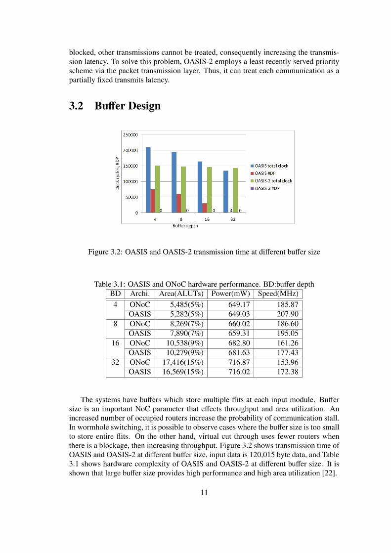
Figure 3.2: OASIS and OASIS-2 transmission time at different buffer size
Table 3.1: OASIS and ONoC hardware performance. BD:buffer depthBD Archi. Area(ALUTs) Power(mW) Speed(MHz)4 ONoC 5,485(5%) 649.17 185.87
OASIS 5,282(5%) 649.03 207.908 ONoC 8,269(7%) 660.02 186.60
OASIS 7,890(7%) 659.31 195.0516 ONoC 10,538(9%) 682.80 161.26
OASIS 10,279(9%) 681.63 177.4332 ONoC 17,416(15%) 716.87 153.96
OASIS 16,569(15%) 716.02 172.38
The systems have buffers which store multiple flits at each input module. Buffersize is an important NoC parameter that effects throughput and area utilization. Anincreased number of occupied routers increase the probability of communication stall.In wormhole switching, it is possible to observe cases where the buffer size is too smallto store entire flits. On the other hand, virtual cut through uses fewer routers whenthere is a blockage, then increasing throughput. Figure 3.2 shows transmission time ofOASIS and OASIS-2 at different buffer size, input data is 120,015 byte data, and Table3.1 shows hardware complexity of OASIS and OASIS-2 at different buffer size. It isshown that large buffer size provides high performance and high area utilization [22].
11
Code 3.1: XY routing code1 //assign next addresses
2 if (nextport == ‘EAST) next_xaddr = xaddr + 1’b1;3 else if (nextport == ‘WEST) next_xaddr = xaddr - 1’b1;4 else next_xaddr = xaddr;5
6 if (nextport == ‘NORTH) next_yaddr = yaddr + 1’b1;7 else if (nextport == ‘SOUTH) next_yaddr = yaddr - 1’b1;8 else next_yaddr = yaddr;9
10 //evaluate next port
11 if (next_xaddr == xdest) begin12 if (next_yaddr == ydest) route = ‘SELF;13 else if(next_yaddr < ydest) route = ‘NORTH;14 else route = ‘SOUTH;15 end else begin16 if (next_xaddr < xdest) route = ‘EAST;17 else route = ‘WEST;18 end
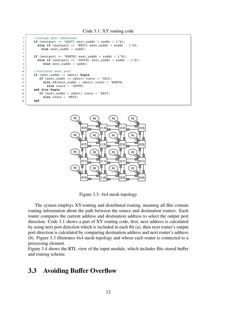
Figure 3.3: 4x4 mesh topology
The system employs XY-routing and distributed routing, meaning all flits containrouting information about the path between the source and destination routers. Eachrouter compares the current address and destination address to select the output portdirection. Code 3.1 shows a part of XY routing code, first, next address is calculatedby using next port direction which is included in each flit (a), then next router’s outputport direction is calculated by comparing destination address and next router’s address(b). Figure 3.3 illustrates 4x4 mesh topology and whose each router is connected to aprocessing element.Figure 3.4 shows the RTL view of the input module, which includes flits stored bufferand routing scheme.
3.3 Avoiding Buffer Overflow
12
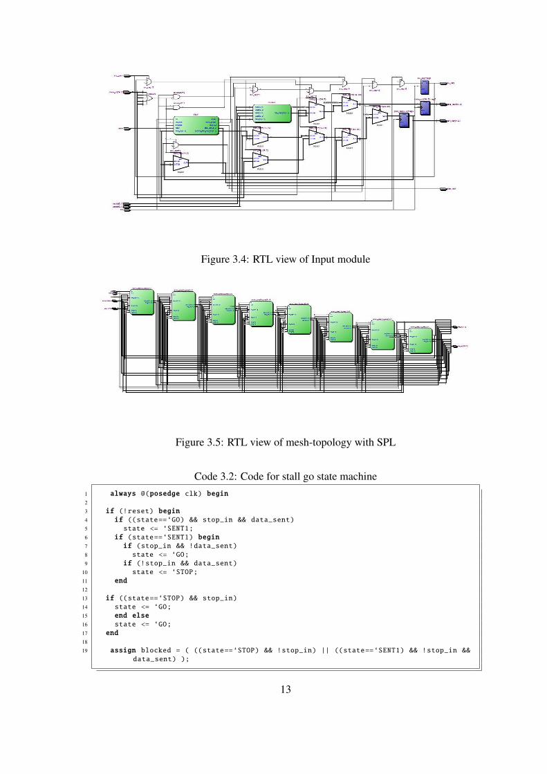
Figure 3.4: RTL view of Input module
Figure 3.5: RTL view of mesh-topology with SPL
Code 3.2: Code for stall go state machine1 always @(posedge clk) begin2
3 if (!reset) begin4 if ((state==‘GO) && stop_in && data_sent)5 state <= ‘SENT1;
6 if (state==‘SENT1) begin7 if (stop_in && !data_sent)8 state <= ‘GO;
9 if (!stop_in && data_sent)10 state <= ‘STOP;
11 end12
13 if ((state==‘STOP) && stop_in)14 state <= ‘GO;
15 end else16 state <= ‘GO;
17 end18
19 assign blocked = ( ((state==‘STOP) && !stop_in) || ((state==‘SENT1) && !stop_in &&data_sent) );
13

Figure 3.6: (a) state machine design for stall go, (b) statement of nearly full signaloutput
Figure 3.7: Stall go block diagram
OASIS-2 employs an avoiding buffer overflow technique instead of OASIS re-transmission flow control (RFC) as flow control. The used avoiding buffer overflowtechnique efficiently prevents buffer from overflowing. Data transfer is controlled bysignals indicating buffer condition. In the absence of stall-go function [23], receivercores need to judge whether there are dropped packets or not. If there are, the trans-mitter must resend the dropped packets using a receiving request signal from mastercores. In addition, stall-go scheme incurs communication blocking, but at the sametime it can considerably reduce latency. Figure 3.6 (a) illustrates the state machine ofthis approach, and (b) shows the input FIFO situation of nearly full signal output. Code3.2 shows how to design the above state machine. State ”Go” indicates the receivingFIFO can store more than two flits. State ”S ent” means that it can store one flit. State”S top” means that it cannot store any more flits. Figure 3.7 illustrates stall-go blockdiagram. There is no state transition from ”S top” to ”S ent”, because once the statetransition ”S top” happens, priority of this port is altered to low in sending router.
3.4 OASIS Arbiter Design
14
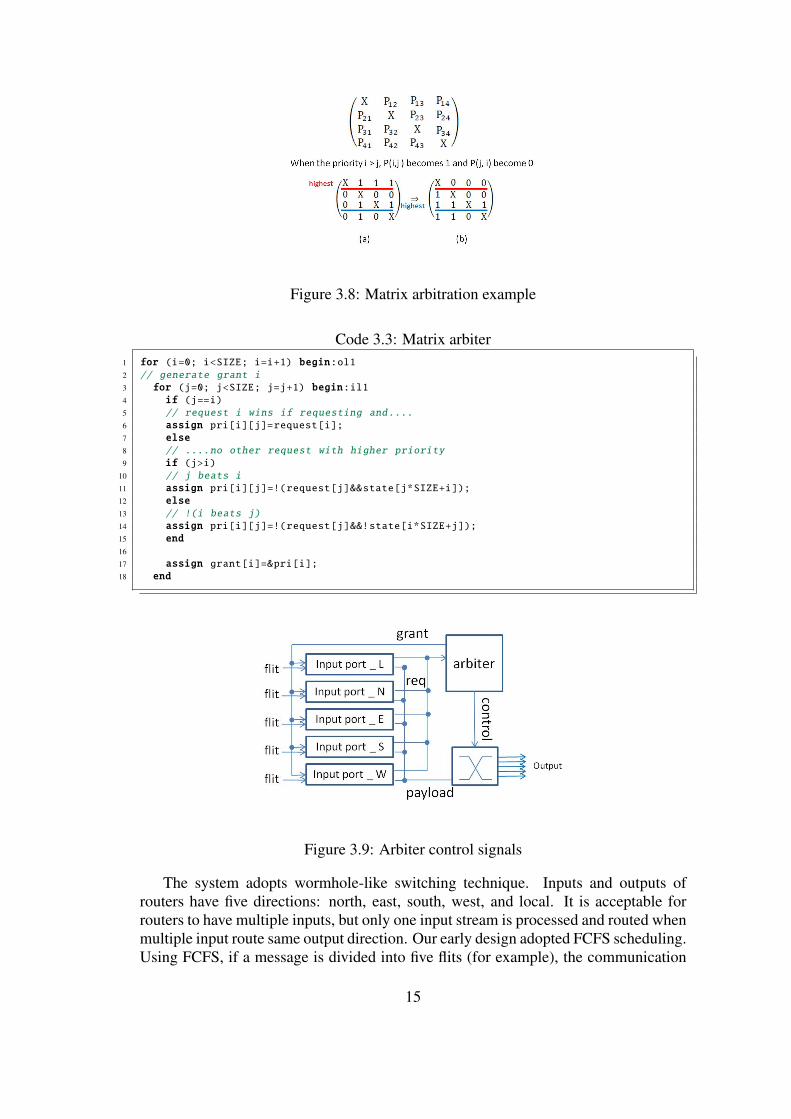
Figure 3.8: Matrix arbitration example
Code 3.3: Matrix arbiter1 for (i=0; i<SIZE; i=i+1) begin:ol12 // generate grant i
3 for (j=0; j<SIZE; j=j+1) begin:il14 if (j==i)5 // request i wins if requesting and....
6 assign pri[i][j]=request[i];7 else8 // ....no other request with higher priority
9 if (j>i)10 // j beats i
11 assign pri[i][j]=!(request[j]&&state[j*SIZE+i]);12 else13 // !(i beats j)
14 assign pri[i][j]=!(request[j]&&!state[i*SIZE+j]);15 end16
17 assign grant[i]=&pri[i];18 end
Figure 3.9: Arbiter control signals
The system adopts wormhole-like switching technique. Inputs and outputs ofrouters have five directions: north, east, south, west, and local. It is acceptable forrouters to have multiple inputs, but only one input stream is processed and routed whenmultiple input route same output direction. Our early design adopted FCFS scheduling.Using FCFS, if a message is divided into five flits (for example), the communication
15

Figure 3.10: RTL view of switch allocator
blocks all routers in the path between source nodes and destination nodes until it fin-ishes transmitting. Because routers are blocked, other transmissions cannot be treated,increasing transmission latency. To solve this problem, our system employs a least re-cently served priority scheme via the packet transmission layer. Thus, it can treat eachcommunication as a partially fixed transmits latency [24], [25]. Matrix arbiter is usedfor a least recently served priority scheme. Figure 3.8 indicates the matrix arbiter, theinputs and outputs of routers have five directions, and one output can be used by max-imum four inputs, so 4 × 4 matrix is used. Each row of the matrix means competitiveinputs, and has priorities. After the highest priority input is served, the priority will bechanged to lowest by inversing one’s row and column. For example, Fig. 3.8 (a) showsan example of how this matrix works: input 1 has the highest priority, after it is served(b), the first row and column values are inverse and input 1 changed to lowest priority.Code 3.3 is a part of the matrix arbiter code. The highest priority input module meansthe row has all 1, so the arbiter gives ”grant” for that. Figure 3.9 shows block diagramof a router with control signals for arbitration.
Figure 3.10 shows RTL view of sw alloc in Fig. 3.1. It includes the schedulingand Avoiding buffer overflow, and Fig. 3.11 shows crossbar RTL view. The RTL isgenerated by a synthesis tool Altera Quartus II.
16

Figure 3.11: RTL view of crossbar
3.5 Abstraction of Target Application
Figure 3.12: Dimension reversal Figure 3.13: Hotspot
The selected target applications are Dimension reversal, Hotspot, and JPEG en-coder. Dimension reversal is a communication method based on transposed matrix,and each node sends messages to another node with an address of the reversed dimen-sion index [26], [27]. Dimension reversal is often used to evaluate the NoC throughputand power consumption, and it includes bottleneck, because of the longest commu-nication exhibited. Figure 3.12 illustrates 4 × 4 dimension reversal. Hotspot meansparticular components receive traffic additionally to the random traffic [28], [29], [30].Hotspot assumed at (1,2) and (2,1) which receive high frequently transmission, andthis type of transaction is assumed frequently for example SRAM access in embeddedsystems. Figure 3.13 illustrates a sample 4 × 4 hotspot communication. Hotspot can
17

Figure 3.14: JPEG encoder block diagram
Figure 3.15: Task Mapping
be avoided using another routing path or another physical wire. JPEG encoder [31]has processing modules for each process instead of CPU implementation. The JPEGencoder task graph is shown in Fig.3.14, JPEG encoder process is contracted by someprocessing modules, and the processes can be divided into RGB data loading, RGB toYUV conversion, Y, Cr, Cb calculations (derivation, quantization and Huffman encod-ing), JPEG data stream checker which judges input data from synchronization 0xFFis a JPEG data or JPEG maker information, and JPEG coded data storing. The Y, Cr,Cb calculation have no data dependency, so they are executed in parallel, but the syn-chronization module synchronizes these three data, so it needs to wait all calculationfinish. The 8 tasks are manually mapped and each one of them is connected to a routeras shown in Fig.3.15. Each task needs a Network Interface (NI) in order to be con-nected to the network. The NI disassembles the incoming data from the transmittingPE, generates flits, and then reassembles them to deliver the compete message to thecorresponding receiving PE.
3.6 Network Interface (NI) DesignFirst, before starting with the NI design, I should set the flit structure. A message,
which is the actual data of each processing element (PE), is divided into some pay-
18
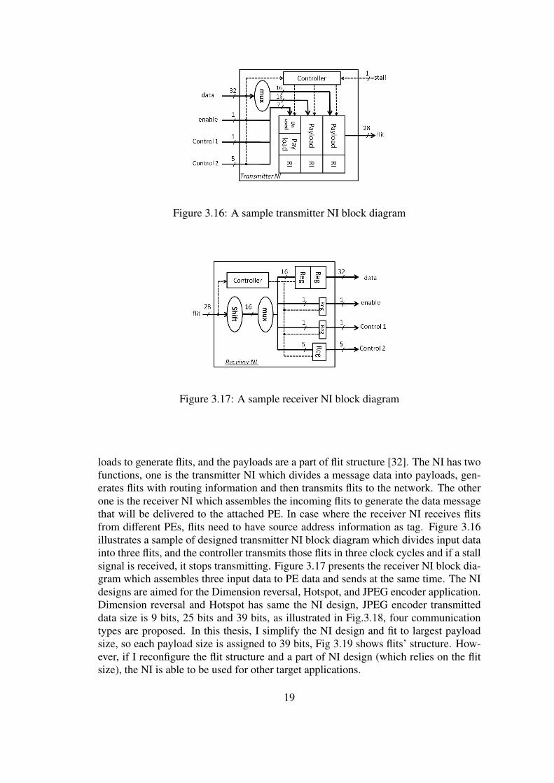
Figure 3.16: A sample transmitter NI block diagram
Figure 3.17: A sample receiver NI block diagram
loads to generate flits, and the payloads are a part of flit structure [32]. The NI has twofunctions, one is the transmitter NI which divides a message data into payloads, gen-erates flits with routing information and then transmits flits to the network. The otherone is the receiver NI which assembles the incoming flits to generate the data messagethat will be delivered to the attached PE. In case where the receiver NI receives flitsfrom different PEs, flits need to have source address information as tag. Figure 3.16illustrates a sample of designed transmitter NI block diagram which divides input datainto three flits, and the controller transmits those flits in three clock cycles and if a stallsignal is received, it stops transmitting. Figure 3.17 presents the receiver NI block dia-gram which assembles three input data to PE data and sends at the same time. The NIdesigns are aimed for the Dimension reversal, Hotspot, and JPEG encoder application.Dimension reversal and Hotspot has same the NI design, JPEG encoder transmitteddata size is 9 bits, 25 bits and 39 bits, as illustrated in Fig.3.18, four communicationtypes are proposed. In this thesis, I simplify the NI design and fit to largest payloadsize, so each payload size is assigned to 39 bits, Fig 3.19 shows flits’ structure. How-ever, if I reconfigure the flit structure and a part of NI design (which relies on the flitsize), the NI is able to be used for other target applications.
19

Figure 3.18: JPEG encoder packet transmission patterns
20

Figure 3.19: Flits’ structure
Figure 3.20: Sample of Shot Pass Link
3.7 Short Pass Link (SPL) ApproachIn Mesh topologies designs, there is a possibility that some transactions may need
larger latency or a lot of hops, and then it may become a bottleneck. To solve theseproblems, Short Pass Link (SPL) is proposed. Figure 3.20 illustrates a simple exampleof SPL. An ONoC router has 5 direction’s in-out ports (North, East, South West, andLocal), but in order to realize SPL, an additional sixth port is needed for the Extra port.However, an additional port increases the area occupation and power consumption.Therefore, the SPL is inserted only between specific communications which includethe possibilities to become a bottleneck among the whole communication patterns. Ifa lot of SPLs are inserted without moderation, this may consume not only large areabut also high power consumption. In order to avoid these problems, an available SPLbudget should be carefully set.
3.7.1 SPL Insertion AlgorithmThis algorithm selects the communications which need a SPL. First, I should de-
cide the available SPL resource budget so I can prevent the increasing area utilizationand power consumption, which are the drawback of SPL addition. Next, I calculateand get the communication costs for all communications patterns with their communi-cation frequencies and distances. Depending on these calculations, the SPL is insertedto the highest cost communication. Simulation and comparison result step which com-pares updated design and pre-updated design and check if there are possibilities for theSPL insertion to reduce the performance. After adding the SPL, the algorithm goes
21
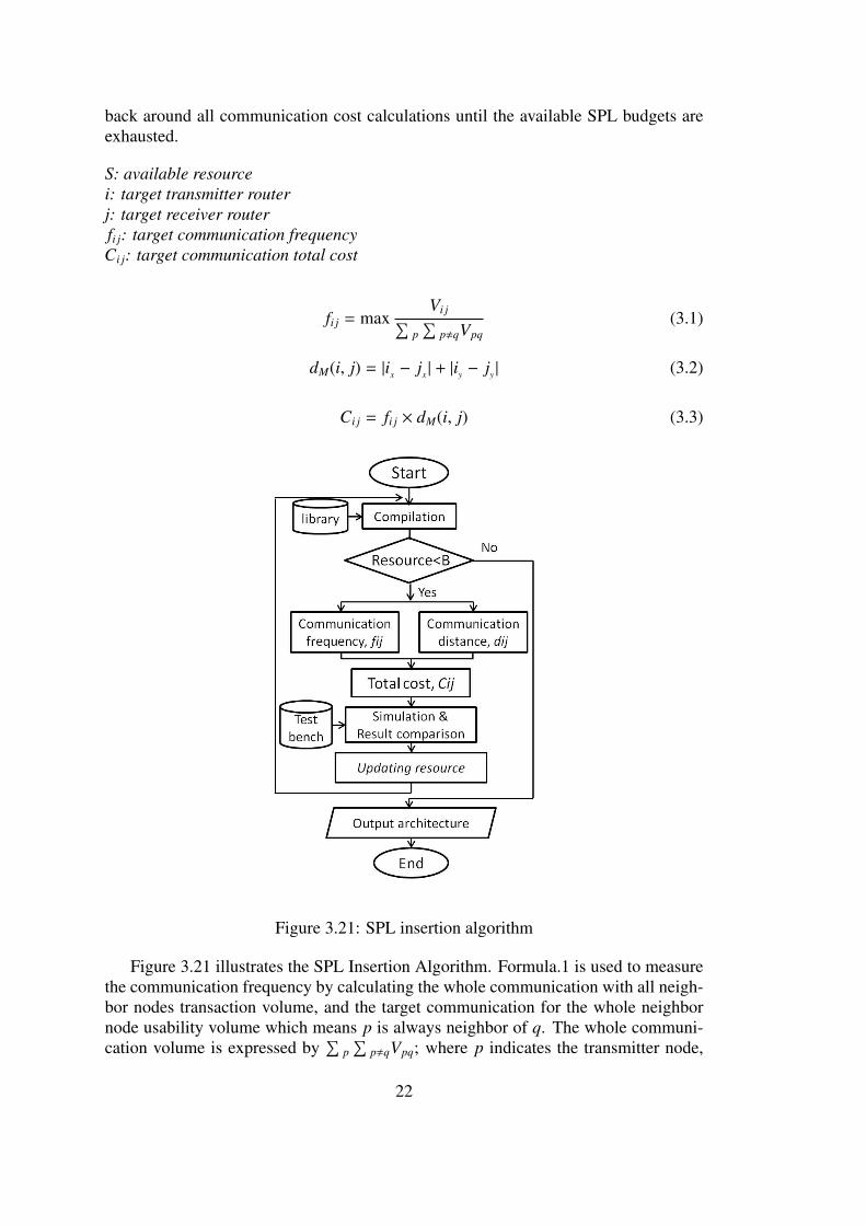
back around all communication cost calculations until the available SPL budgets areexhausted.
S: available resourcei: target transmitter routerj: target receiver routerfi j: target communication frequencyCi j: target communication total cost
fi j = maxVi j∑
p∑
p,qVpq(3.1)
dM(i, j) = |ix − jx | + |iy − jy | (3.2)
Ci j = fi j × dM(i, j) (3.3)
Figure 3.21: SPL insertion algorithm
Figure 3.21 illustrates the SPL Insertion Algorithm. Formula.1 is used to measurethe communication frequency by calculating the whole communication with all neigh-bor nodes transaction volume, and the target communication for the whole neighbornode usability volume which means p is always neighbor of q. The whole communi-cation volume is expressed by
∑p∑
p,qVpq; where p indicates the transmitter node,
22
q indicates the receiver node, p and q are always neighbor. Then, The target commu-nication frequency is expressed by Vi j; where i indicates the transmitter node, and jindicates the receiver node. To calculate distance of communications, Manhattan dis-tance is employed (Formula.2), the address of i is expressed by (ix, iy), and the addressof j is expressed by ( jx, jy). Finally, the cost calculation is computed (Formula.3) usingvalues from (1) and (2).
3.7.2 Additional Ports Area Utilization
Table 3.2: 5-ports OASIS Router Area UtilizationParameters Input module Switch Allocator Crossbar TotalALUTs 1-port 71(7.4%) 300(31%) 310(32.1%) 965
5-ports 355(36.8%)Registers 1-port 72(15.2%) 90(18.9%) 25(5.3%) 475
5-ports 360(75.8%)
Table 3.3: 6-ports OASIS Router Area UtilizationParameters Input module Switch Allocator Crossbar TotalALUTs 1-port 75(5.8%) 469(36.5%) 366(28.5%) 1285
6-ports 450(35%)Registers 1-port 99(13.3%) 144(19.4%) 36(4.8%) 744
6-ports 594(79.8%)
The logic structure of Stratix III devices delivers unprecedented performance andlogic efficiency. This logic structure is built from basic logic units known as adaptivelogic modules (ALMs). Each ALM contains a variety of (look-up table) LUT-basedresources, two full adders, carry-chain segments, two flip flops, and many additionallogic enhancements that can be flexibly divided into two adaptive LUTs (ALUTs) [33].Quartus II compilation report shows logic utilization which includes combinationalALUTs, memory ALUTs and dedicated logic registers. In my design, combinationalALUTs and dedicated logic registers are mostly used. Table 3.2 shows a 5-ports routerarea utilization and table 3.3 shows a 6-ports router area utilization, The 6 ports router’sALUTs utilization increases 33.2% and registers utilization increase 56.6%. OASIShas identical routers for all nodes, so if somewhere that needs additional port by SPLs,it significantly increases area utilization. If designers insert a lot of SPLs, the areautilization significantly increase, so it is recommended to consider design restrictions.
3.7.3 Modifications for SPLThe proposed low latency, Optimized OASIS NoC system (ONoC) is a highly opti-
mized for target application based on OASIS-2. The main ONoC modifications are: an
23
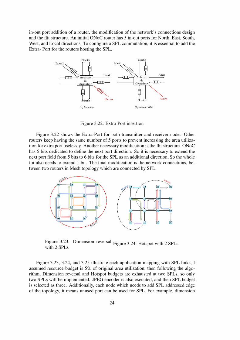
in-out port addition of a router, the modification of the network’s connections designand the flit structure. An initial ONoC router has 5 in-out ports for North, East, South,West, and Local directions. To configure a SPL commutation, it is essential to add theExtra- Port for the routers hosting the SPL.
Figure 3.22: Extra-Port insertion
Figure 3.22 shows the Extra-Port for both transmitter and receiver node. Otherrouters keep having the same number of 5 ports to prevent increasing the area utiliza-tion for extra port uselessly. Another necessary modification is the flit structure. ONoChas 5 bits dedicated to define the next port direction. So it is necessary to extend thenext port field from 5 bits to 6 bits for the SPL as an additional direction, So the wholeflit also needs to extend 1 bit. The final modification is the network connections, be-tween two routers in Mesh topology which are connected by SPL.
Figure 3.23: Dimension reversalwith 2 SPLs
Figure 3.24: Hotspot with 2 SPLs
Figure 3.23, 3.24, and 3.25 illustrate each application mapping with SPL links, Iassumed resource budget is 5% of original area utilization, then following the algo-rithm, Dimension reversal and Hotspot budgets are exhausted at two SPLs, so onlytwo SPLs will be implemented. JPEG encoder is also executed, and then SPL budgetis selected as three. Additionally, each node which needs to add SPL addressed edgeof the topology, it means unused port can be used for SPL. For example, dimension
24
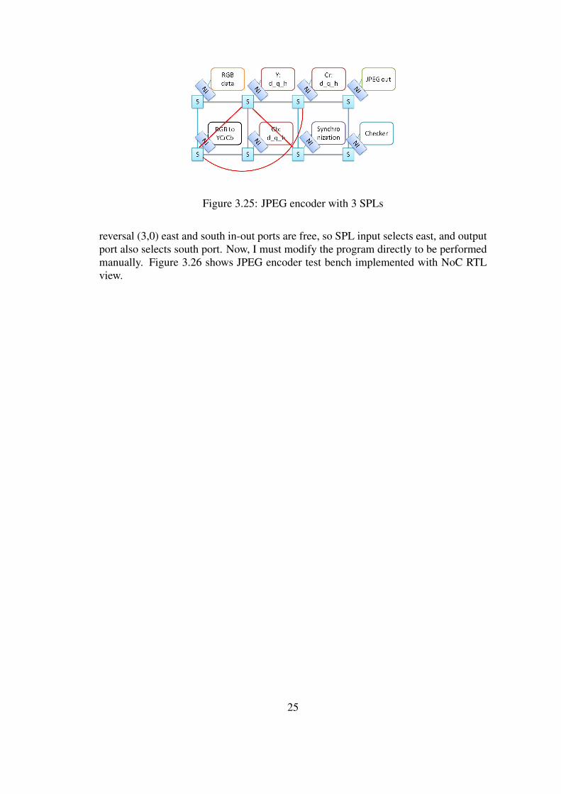
Figure 3.25: JPEG encoder with 3 SPLs
reversal (3,0) east and south in-out ports are free, so SPL input selects east, and outputport also selects south port. Now, I must modify the program directly to be performedmanually. Figure 3.26 shows JPEG encoder test bench implemented with NoC RTLview.
25

Figure 3.26: RTL view of NoC with JPEG encoder
26

Chapter 4
Evaluation Results
The proposed low latency, Optimized OASIS NoC system (ONoC) is a highly opti-mized version with SPL insert algorithm of our earlier designed architecture (OASIS-2). In this chapter, I would like to explain the comparison OASIS-2 and ONoC withSPL algorithm at the hardware and execution time.As explained in Chap. 3.5, the target applications are Dimension Reversal, Hotspotand JPEG encoder. Each application is designed in Verilog-HDL.
4.1 Environments and ParametersThe proposed architecture is designed in Verilog-HDL. Synthesis with industrial
CAD tools (Altera Quartus II ver. 11.0), and simulated with ModelSim-Altera 6.6.The target device is Altera Stratix III EP3SL150F1152C2. Table 4.1 shows design andsimulation parameters for Dimension reversal test case, input data is continuously in-jected, both transmitter and receiver nodes are assigned (6 nodes), and each transmitternode sends one thousand flits, and receivers verifies receiving flits. Table 4.2 shows de-sign and simulation parameters for Hotspot test case. The both transmitter and receivernodes are equal to 8 nodes and continuously injecting flits. Each transmitter sends onethousand flits, and receivers verify received flits. The Dimension reversal and Hotspottransmit the random number traffic. There are no calculations at PEs, so clock is setto only one type. Table 4.3 shows JPEG encoder design and simulation parameters.Input RGB data is inputted into the RGB data module. Input RGB data ratio is 96×96(27,906 bytes). The input to the module is a 24-bit data bus with 8 bits each for theRed pixel, Green pixel, and Blue pixel. JPEG encoder whose specifications strict themaximum clock speed, and each PE waits receiving input data, so there are two typesof clock cycles are defined clock for JPEG encoder and network interconnection. Ouralgorithm (Fig.3.21) starts from budget selection, the budget is assumed to 5% of extrahardware of original design’s.
4.2 Dimension Reversal and Hotspot Simulation ResultsIn this section, the simulation results will be explained. The number of SPL de-
pends on the budget selection. The budget is assumed to 5% extra hardware of original
27

Table 4.1: Dimension reversal simulation environmentParameters OASIS-2 ONoC with SPLTopology Mesh Mesh with SPLBudget 0 5%
Flow control ACK/NACK(at PE) Stall goRouting Algorithm XY-routing XY-routingSwitching Method Wormhole Wormhole
Flit Size 28 bit 28 bitBuffer Depth 4 4
Table 4.2: Hotspot simulation environmentParameters OASIS-2 ONoC with SPLTopology Mesh Mesh with SPLBudget 0 5%
Flow control ACK/NACK(at PE) Stall goRouting Algorithm XY-routing XY-routingSwitching Method Wormhole Wormhole
Flit Size 28 bit 28 bitBuffer Depth 4 4
Table 4.3: JPEG encoder simulation environmentParameters OASIS-2 ONoC with SPLTopology Mesh Mesh with SPLBudget 0 5%
Flow control ACK/NACK(at PE) Stall goRouting Algorithm XY-routing XY-routingSwitching Method Wormhole Wormhole
Flit Size 55 bit 55 bitBuffer Depth 4 4
28
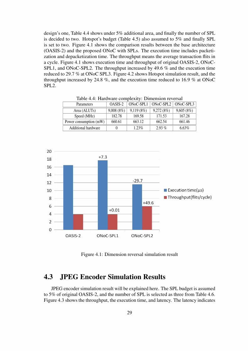
design’s one, Table 4.4 shows under 5% additional area, and finally the number of SPLis decided to two. Hotspot’s budget (Table 4.5) also assumed to 5% and finally SPLis set to two. Figure 4.1 shows the comparison results between the base architecture(OASIS-2) and the proposed ONoC with SPLs. The execution time includes packeti-zation and depacketization time. The throughput means the average transaction flits ina cycle. Figure 4.1 shows execution time and throughput of original OASIS-2, ONoC-SPL1, and ONoC-SPL2. The throughput increased by 49.6 % and the execution timereduced to 29.7 % at ONoC SPL3. Figure 4.2 shows Hotspot simulation result, and thethroughput increased by 24.8 %, and the execution time reduced to 16.9 % at ONoCSPL2.
Table 4.4: Hardware complexity: Dimension reversalParameters OASIS-2 ONoC-SPL1 ONoC-SPL2 ONoC-SPL3
Area (ALUTs) 9,008 (8%) 9,119 (8%) 9,272 (8%) 9,605 (8%)Speed (MHz) 182.78 169.58 171.53 167.28
Power consumption (mW) 660.61 663.12 662.54 661.46Additional hardware 0 1.23% 2.93 % 6.63%
Figure 4.1: Dimension reversal simulation result
4.3 JPEG Encoder Simulation ResultsJPEG encoder simulation result will be explained here. The SPL budget is assumed
to 5% of original OASIS-2, and the number of SPL is selected as three from Table 4.6.Figure 4.3 shows the throughput, the execution time, and latency. The latency indicates
29
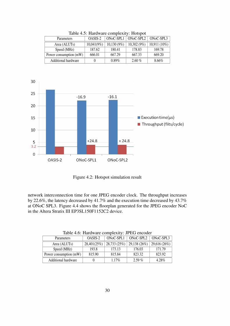
Table 4.5: Hardware complexity: HotspotParameters OASIS-2 ONoC-SPL1 ONoC-SPL2 ONoC-SPL3
Area (ALUTs) 10,041(9%) 10,130 (9%) 10,302 (9%) 10,911 (10%)Speed (MHz) 187.62 180.41 178.83 169.78
Power consumption (mW) 666.01 667.29 667.33 669.20Additional hardware 0 0.89% 2.60 % 8.66%
Figure 4.2: Hotspot simulation result
network interconnection time for one JPEG encoder clock. The throughput increasesby 22.6%, the latency decreased by 41.7% and the execution time decreased by 43.7%at ONoC SPL3. Figure 4.4 shows the floorplan generated for the JPEG encoder NoCin the Altera Stratix III EP3SL150F1152C2 device.
Table 4.6: Hardware complexity: JPEG encoderParameters OASIS-2 ONoC-SPL1 ONoC-SPL2 ONoC-SPL3
Area (ALUTs) 28,401(25%) 28,733 (25%) 29,138 (26%) 29,616 (26%)Speed (MHz) 193.8 173.13 176.03 171.79
Power consumption (mW) 815.90 815.84 823.32 823.92Additional hardware 0 1.17% 2.59 % 4.28%
30

Figure 4.3: JPEG encoder simulation result
4.4 Hardware Design AnalysisThe hardware complexity analysis will be explained in this section, Altera Quartus
II report, which shows the area utilization, clock speed, and this tool provides PowerAnalysis tools to estimate power consumption [34], TimeQuest Timing Analyzer isalso supported by the tool and it shows FMAX for every clock in the design, regardlessof the user-specified clock periods. FMAX is only computed for paths where the sourceand destination registers or ports are driven by the same clock [35]. Target devicehas 113,600 ALUTs, each table shows area utilization ratio based on the number ofALUTs. The area of these three test benches in ONoC which has SPL increased under5%, the Dimension reversal increased by 2.93%, the Hotspot increased by 2.60%, theJPEG encoder increased by 4.28%.
4.5 Power Consumption AnalysisTo analyze power consumption, the Altera Quartus II PowerPlay Power Analysis
accurately estimates our design power consumption. These three simulations are an-alyzed with ModelSim-Altera gate-level simulation. The power analysis tool, Signalactivity and static probability information derive from a Verilog Value Change DumpFile [34]. Table 4.4, 4.5, and 4.6 also show power consumptions. Dimension rever-sal ONoC SPL2 increased by 1.93 mW (0.29%), Hotspot ONoC SPL1 increased by
31

1.32 mW (0.20%), and JPEG encoder ONoC SPL3 increased by 8.02 mW (0.98%).Every result shows increasing power consumption a little. The power consumption isestimated by dynamic power dissipation, static power dissipation, and I/O power dissi-pation. SPLs insertion affects dynamic and static power dissipations, both parametersincrease slightly.
32

Figure 4.4: Chip floor plan for JPEG encoder system implementation
33

Chapter 5
Conclusion
In this thesis, I presented architecture, design, and evaluation of a Network-on-Chiparchitecture which utilizes several advanced optimization techniques. The softwareNoC simulation tools are not enough to evaluate accurate a NoC parameters’ effectsand trade-offs, it is not accurate hardware complexity and performance, because it usesmany assumptions and approximations. So, I prototyped the system in hardware andevaluated its performance in terms of execution time, area utilization, and power usingDimension reversal transaction, Hotspot transaction, and a parallelized JPEG encoder.OASIS NoC employs mesh topology which is no careful consideration for given ap-plications, but designing customized topology takes long time and it may occupy largearea utilizations, so I proposed SPL insertion algorithm to reduce latency which di-rectly affect performance. The algorithm selects which communications are needed toinsert a SPL, and the number of SPLs is decided by depending on hardware budgets.From the performance evaluation results, I conclude that the Dimension reversal exe-cution time in ONoC decreased by 29.7%, when compared to the original base archi-tecture, and Hotspot execution time decreased by 16.9%, and JPEG encoder decreasedby 43.7% The area of these three test benches in ONoC which has SPL increased under5%, the Dimension reversal increased by 2.93%, the Hotspot increased by 2.60%, theJPEG encoder increased by 4.28%, and the power consumption slightly increased by0.49% on average. The results indicate that the architecture is effective in balancingthe power and performance of NoC design.
34
References
[1] A. Ben Abdallah, and M. Sowa, Basic Network-on-Chip Interconnection forFuture Gigascale MCSoCs Applications: Communication and ComputationOrthogonalization, In Proceedings of Tunisia-Japan Symposium on Society,Science and Technology (TJASSST), Dec. 4-9th, 2006.
[2] F. G. Moraes, ; et al., HERMES: an Infrastructure for Low Area OverheadPacket-Switching Networks on Chip, Integration, the VLSI Journal, vol. 38-1,2004, pp. 69-93.
[3] F. A. Samman, T. Hollstein, and M. Glesner, ”Multicast parallel pipeline routerarchitecture for network-on-chip,” in Proceedings of the Conference on De-sign, Automation and Test in Europe (DATE ’08), pp. 1396―1401, Munich,Germany, March 2008.
[4] S. Kumar, A. Jantsch, J.-P. Soininen, M. Forsell, et al., ”A Network on ChipArchitecture and Design Methodology”,VLSI, 2002. Proceedings. IEEE Com-puter Society Annual Symposium, April 25-26, 2002 p105 - 112
[5] N. Genko, G. De Micheli, D. Atienza, J. Mendias, R. Hermida, and F. Catthoor,”A complete network-on-chip emulation framework,” in Proc. Des., Autom.Test Eur. Conf., Mar. 2005, pp. 246―251.
[6] R. Holsmark, A. Johansson, and S. Kumar,“ On connecting cores to packetswitched on-chip networks: A case study with MicroBlaze processor cores,”7th IEEE Workshop DDECS 04, april 2004.
[7] P. P. Pande, C. Grecu, M. Jones, A. Ivanov, and R. Saleh, ”Performance eval-uation and design trade-offs for network-on-chip interconnect architectures,”IEEE Transactions on Computers, vol. 54, no. 8, pp. 1025―1040, Aug. 2005.
[8] ARM, ”Advanced microprocessor bus architecture (AMBA) specification,v.2.0, 1999”, http://www.arm.com/
[9] R. A. Shafik, P. Rosinger and B. M. Al-Hashimi, ”MPEG-based PerformanceComparison between Network-on-Chip and AMBA MPSoC”, 2008 IEEE De-sign and Diagnostics of Electronic Circuits and Systems, 16-18 April, 2008,Bratislava, Slovakia. pp. 98-103
[10] H. G. Lee, N. Chang, U.Y. Ogras, and Marculescu, R. ”On-chip communica-tion architecture exploration: A quantitative evaluation of point-to-point, bus,
35

and network-on-chip approaches”, ACM Transactions on Design Automationof Electronic Systems (TODAES), 2007
[11] A. JALABERT, MURALI, S., BENINI, L., ANDMICHELI, G. D.XpipesCompiler: A tool for instantiating application specific networks-on-chip. In Proceedings of Design, Automation and Testing in Europe Conference.IEEE, p884―889. 2004.
[12] S. Murali and G. De Micheli, ”SUNMAP: A Tool for Automatic TopologySelection and Generation for NoCs,” Proc. Design Automation Conf., 2004.
[13] K. Srinivasan, et. al. Linear programming based techniques for synthesis ofNetwork-on-Chip architectures. In Proc. ICCD, 2004.
[14] A. V. de Mello, L. C. O. F. G. Moraes, and N. L. V. Calazans. Evaluation ofrouting algorithms on mesh based NoCs. Technical report, FACULDADE DEINFORM´ATICA - PUCRS, Brazil, 2004.
[15] M. Li, Q.-A. Zeng, and W.-B. Jone, ”DyXY - a proximity congestion-awaredeadlock-free dynamic routing method for network on chip,” in Proc. of De-sign Automation Conference, pp. 849-852, 2006.
[16] L. Bononi and N. Concer. Simulation and Analysis of Network on Chip Archi-tectures: Ring, Spidergon and 2D Mesh. DATE, pages 154-159, 2006.
[17] E. BOLOTIN , I. CIDON, R. GINOSAUR, AND A. KOLODNY, ”QNoC: QoSarchitecture and design process for network-on-chip” J. Syst. Archit. 2004.
[18] M. S. Rasmussen, ”Network-on-Chip in Digital Hearing Aids”, Informat-ics and Mathematical Modelling, Technical University of Denmark, DTU,Richard Petersens Plads, Building 321, DK-2800 Kgs. Lyngby, IMM-Thesis-2006-76, 2006.
[19] A. Pullini, F. Angiolini, D. Bertozzi, and L. Benini, ”Fault tolerance overheadin network-on-chip flow control schemes,” in Proc. Symp. Integr. Circuits Syst.Des., Sep. 2005, pp. 224-229.
[20] P. P. Pande, C. Grecu, M. Jones, A. Ivanov, and R. Saleh, ”Performance eval-uation and design trade-offs for network-on-chip interconnect architectures,”IEEE Trans. Comput., vol. 54, no. 8, pp. 1025―1040, Aug. 2005.
[21] K. Goossens, , J. Dielissen, and A. Radulescu, ”The thereal network on chip:Concepts, architectures, and implementations.” IEEE Design and Test of Com-puters. 2005.
[22] K. Mori, A. Esch, A. Ben Abdallah, K., Kuroda, ”Advanced Design Issuefor OASIS Network-on-Chip Architecture , IEEE, International Conferenceon BWCCA, p.74-79, 2010.
36
[23] K. Mori, A. Ben Abdallah, K. Kuroda, ”Design and Evaluation of a Complex-ity Effective Network-on-Chip Architecture on FPGA”, The 19th IntelligentSystem Symposium (FAN 2009), Sep. 2009, pp.318-321.
[24] B. T. Gold. ”Balancing Performance, Area, and Power in an On-Chip Net-work.”, Master’s thesis, Department of Electrical and Computer Engineering,Virginia Tech, August 2004.
[25] Z, Fu and X. Ling ”The design and implementation of arbiters for Network-on-chips.” IEEE, Industrial and Information Systems (IIS), 2010 2nd InternationalConference, vol. 1, p. 292-295, 2010
[26] M. M. Hafizur Rahman and S. Horiguchi. ”High performance hierarchicaltorus network under matrix transpose traffic patterns”, In Proc. 7th Interna-tional Symposium on Parallel Architectures, Algorithms and Netowrks (IS-PAN ’04), Hong Kong, China, May 2004.
[27] A. A. Chien and J. H. Kim, ”Planar-Adaptive Routing: Low-Cost AdaptiveNetworks for Multiprocessors”, J. ACM, vol.42, no.1, pp.91-123, Jan.1995.
[28] T. Schonwald , J. Zimmermann, Bringmann, O. Rosenstiel, W., ”Fully Adap-tive Fault-tolerant Routing Algorithm for Network-on-Chip Architectures”,Proc. 10th Euromicro Conf. on Digital System Design Architectures, Meth-ods and Tools, p.527-534, 2007.
[29] V. Catania, R. Holsmark, S. Kumar, and M. Palesi, ”A methodology for designof application specific deadlock-free routing algorithms for NoC systems,” inProc. Int. Conf. Hardware-Softw. Codesign Syst. Synthesis, Oct. 2006, pp. 142―147.
[30] Li, X. and Hammami, O., ”Network-on-Chip Performance Evaluation by on-Chip Hardware Monitoring Network: OCP-IP Benchmarks on 48-core”, DAC2011 Workshop on Diagnostic Services in Network-on-Chips, June 5, 2011.
[31] ”OpenCores”, http://opencores.org/
[32] R. G. Olsen, ”OCP Based Adapter for Network-on-Chip.” Master Degree,Technical University of Denmark, 2005.
[33] Altera, ”http://www.altera.com/devices/fpga/stratix-fpgas/stratix-ii/stratix-ii/features/architecture/st2-lut.html”, (29 January, 2012 access)
[34] Quartus II Handbook Version 11.0 Volume 3: Verification, Chapter 10: Pow-erPlay Power Analysis, Altera Corporation, December 2010.
[35] Quartus II Handbook Version 11.0 Volume 3: Verification, Chapter 6: TheQuartus II TimeQuest Timing Analyzer, Altera Corporation, May 2011.
37
Publication
1. Kenichi Mori, ”Optimizations Techniques and FPGA Prototyping of OASISNetwork-on-Chip”, Graduation Thesis, The University of Aizu, Feb. 2010.
2. Kenichi Mori, A. Ben Abdallah, Kenichi Kuroda, Design and Evaluation of aComplexity Effective Network-on-Chip Architecture on FPGA, The 19th Intel-ligent System Symposium (FAN 2009), pp.318-321, Sep. 2009,
3. Kenichi Mori, Adam Esch, A. Ben Abdallah, Kenichi Kuroda, ”Advanced De-sign Issue for OASIS Network-on-Chip Architecture , IEEE, International Con-ference on Broadband, Wireless Computing, Communication and Applications,pp.74-79, 2010
38